EP3043470A1 - High frequency signal amplifying circuitry - Google Patents
High frequency signal amplifying circuitry Download PDFInfo
- Publication number
- EP3043470A1 EP3043470A1 EP16150170.5A EP16150170A EP3043470A1 EP 3043470 A1 EP3043470 A1 EP 3043470A1 EP 16150170 A EP16150170 A EP 16150170A EP 3043470 A1 EP3043470 A1 EP 3043470A1
- Authority
- EP
- European Patent Office
- Prior art keywords
- amplifier
- high frequency
- frequency signal
- loop oscillation
- carrier
- Prior art date
- Legal status (The legal status is an assumption and is not a legal conclusion. Google has not performed a legal analysis and makes no representation as to the accuracy of the status listed.)
- Granted
Links
- 230000010355 oscillation Effects 0.000 claims abstract description 148
- 239000000758 substrate Substances 0.000 claims description 6
- 239000004065 semiconductor Substances 0.000 claims description 3
- 238000010586 diagram Methods 0.000 description 14
- 230000005669 field effect Effects 0.000 description 5
- 230000003321 amplification Effects 0.000 description 3
- 238000003199 nucleic acid amplification method Methods 0.000 description 3
- 230000001629 suppression Effects 0.000 description 3
- 239000003990 capacitor Substances 0.000 description 2
- 238000012986 modification Methods 0.000 description 2
- 230000004048 modification Effects 0.000 description 2
- 238000013459 approach Methods 0.000 description 1
- 230000000052 comparative effect Effects 0.000 description 1
- 230000001934 delay Effects 0.000 description 1
- 230000000694 effects Effects 0.000 description 1
- 238000005457 optimization Methods 0.000 description 1
- 230000003071 parasitic effect Effects 0.000 description 1
- 238000006467 substitution reaction Methods 0.000 description 1
Images






Classifications
-
- H—ELECTRICITY
- H03—ELECTRONIC CIRCUITRY
- H03F—AMPLIFIERS
- H03F1/00—Details of amplifiers with only discharge tubes, only semiconductor devices or only unspecified devices as amplifying elements
- H03F1/02—Modifications of amplifiers to raise the efficiency, e.g. gliding Class A stages, use of an auxiliary oscillation
- H03F1/0205—Modifications of amplifiers to raise the efficiency, e.g. gliding Class A stages, use of an auxiliary oscillation in transistor amplifiers
- H03F1/0288—Modifications of amplifiers to raise the efficiency, e.g. gliding Class A stages, use of an auxiliary oscillation in transistor amplifiers using a main and one or several auxiliary peaking amplifiers whereby the load is connected to the main amplifier using an impedance inverter, e.g. Doherty amplifiers
-
- H—ELECTRICITY
- H03—ELECTRONIC CIRCUITRY
- H03F—AMPLIFIERS
- H03F1/00—Details of amplifiers with only discharge tubes, only semiconductor devices or only unspecified devices as amplifying elements
- H03F1/08—Modifications of amplifiers to reduce detrimental influences of internal impedances of amplifying elements
- H03F1/083—Modifications of amplifiers to reduce detrimental influences of internal impedances of amplifying elements in transistor amplifiers
- H03F1/086—Modifications of amplifiers to reduce detrimental influences of internal impedances of amplifying elements in transistor amplifiers with FET's
-
- H—ELECTRICITY
- H03—ELECTRONIC CIRCUITRY
- H03F—AMPLIFIERS
- H03F3/00—Amplifiers with only discharge tubes or only semiconductor devices as amplifying elements
- H03F3/189—High-frequency amplifiers, e.g. radio frequency amplifiers
- H03F3/19—High-frequency amplifiers, e.g. radio frequency amplifiers with semiconductor devices only
- H03F3/195—High-frequency amplifiers, e.g. radio frequency amplifiers with semiconductor devices only in integrated circuits
-
- H—ELECTRICITY
- H03—ELECTRONIC CIRCUITRY
- H03F—AMPLIFIERS
- H03F3/00—Amplifiers with only discharge tubes or only semiconductor devices as amplifying elements
- H03F3/60—Amplifiers in which coupling networks have distributed constants, e.g. with waveguide resonators
- H03F3/602—Combinations of several amplifiers
- H03F3/604—Combinations of several amplifiers using FET's
-
- H—ELECTRICITY
- H03—ELECTRONIC CIRCUITRY
- H03F—AMPLIFIERS
- H03F2200/00—Indexing scheme relating to amplifiers
- H03F2200/153—Feedback used to stabilise the amplifier
-
- H—ELECTRICITY
- H03—ELECTRONIC CIRCUITRY
- H03F—AMPLIFIERS
- H03F2200/00—Indexing scheme relating to amplifiers
- H03F2200/451—Indexing scheme relating to amplifiers the amplifier being a radio frequency amplifier
-
- H—ELECTRICITY
- H03—ELECTRONIC CIRCUITRY
- H03F—AMPLIFIERS
- H03F2203/00—Indexing scheme relating to amplifiers with only discharge tubes or only semiconductor devices as amplifying elements covered by H03F3/00
- H03F2203/45—Indexing scheme relating to differential amplifiers
- H03F2203/45528—Indexing scheme relating to differential amplifiers the FBC comprising one or more passive resistors and being coupled between the LC and the IC
Definitions
- Embodiments described herein relate generally to a high-frequency signal amplifying circuitry.
- a Doherty amplifier that efficiently amplifies a backed-off high frequency signal has been known.
- a Doherty amplifier includes a carrier amplifier and a peak amplifier connected in parallel and combines and outputs the high frequency signals amplified by the carrier amplifier and the peak amplifier.
- a Doherty amplifier is connected in parallel with another Doherty amplifier, the same signal being divided to and amplified by the Doherty amplifier as the other Doherty amplifier. In this case, depending upon the circuit conditions, loop oscillation might occur between the Doherty amplifiers.
- the high frequency signal amplifying circuitry may include, but is not limited to, a first splitter, a first amplifier, a second amplifier, and a first loop oscillation suppressor.
- the first amplifier includes a second splitter that divides a signal supplied from the first splitter, a first carrier amplifier, a first peak amplifier, and a first combiner that combines signals output from the first carrier amplifier and from the first peak amplifier.
- the second amplifier -includes a third splitter that divides a signal supplied from the first splitter, a second carrier amplifier, a second peak amplifier, and a second combiner that combines signals output from the second carrier amplifier and from the second peak amplifier.
- the second carrier amplifier is adjacent to an associated the first carrier amplifier or the second peak amplifier is adjacent to an associated the first peak amplifier.
- the first loop oscillation suppressor locates between the second carrier amplifier and the associated first carrier amplifier or the second peak amplifier and the associated first peak amplifier.
- the third combiner combines signals output from the first combiner and the second combiner.
- the first loop oscillation suppressor may be disposed between the second carrier amplifier and the associated first carrier amplifier or the second peak amplifier and the associated first peak amplifier.
- the first loop oscillation suppressor may be electrically connected between the second carrier amplifier and the associated first carrier amplifier or the second peak amplifier and the associated first peak amplifier.
- the first loop oscillation suppressor may connect between locations of the second carrier amplifier and the associated first carrier amplifier or the second peak amplifier and the associated first peak amplifier.
- the first loop oscillation suppressor connects either first and second nodes or third and fourth nodes.
- the first and second nodes are inputs of the first and second amplifiers, respectively.
- the third and fourth nodes are outputs of the first and second amplifiers, respectively.
- the first and second nodes are inputs of the first and second amplifiers, respectively, and the first and second nodes are to have a first potential.
- the third and fourth nodes are outputs of the first and second amplifiers, respectively, and the third and fourth nodes are to have a second potential which is different from the first potential.
- the first loop oscillation suppressor includes a resistor.
- the high frequency signal amplifying circuitry may include, but is not limited to, a second loop oscillation suppressor; a third amplifier; and a fourth amplifier.
- the third amplifier includes a fourth splitter that divides a signal supplied from the first splitter, a third carrier amplifier, a third peak amplifier, and a fourth combiner that combines signals output from the third carrier amplifier and from the third peak amplifier.
- the fourth amplifier -includes a fifth splitter that divides a signal supplied from the first splitter, a fourth carrier amplifier, a fourth peak amplifier, and a fifth combiner that combines signals output from the fourth carrier amplifier and from the fourth peak amplifier.
- the fourth carrier amplifier is adjacent to an associated the third carrier amplifier or the fourth peak amplifier is adjacent to an associated the third peak amplifier.
- the third combiner combines signals output from the first combiner, the second combiner, the fourth combiner and the fifth combiner.
- a first pair of the first and second amplifiers is adjacent to a second pair of the third and fourth amplifiers.
- the second loop oscillation suppressor locates between the fourth carrier amplifier and the associated third carrier amplifier or the fourth peak amplifier and the associated third peak amplifier.
- the third loop oscillation suppressor may located between the first pair of the first and second amplifiers and the second pair of the third and fourth amplifiers.
- At least one of the first carrier amplifier, the first peak amplifier, the second carrier amplifier, the second peak amplifier, the second splitter, the third splitter, the first combiner, the second combiner, the first splitter, the third combiner, and the first loop oscillation suppressor is in a single package.
- the circuitry may include, but is not limited to, a monolithic microwave integrated circuit (MIMIC) on a single semiconductor substrate.
- the MMIC includes a part of a group consisting of: at least a part of the first carrier amplifier, at least a part of the first peak amplifier, at least a part of the second carrier amplifier, at least a part of the second peak amplifier, at least a part of the second splitter, at least a part of the third splitter, at least a part of the first combiner, at least a part of the second combiner, at least a part of the first splitter, at least a part of the third combiner, and at least a part of the first loop oscillation suppressor.
- FIG. 1 is a block diagram showing the constitution of a parallel-connected load type Doherty amplifier 1 in a high frequency signal amplifying apparatus of the embodiment.
- the Doherty amplifier 1 is inputted a high frequency signal and outputs an amplified high frequency signal to a non-illustrated antenna.
- the Doherty amplifier 1 includes an input terminal 10, a matching circuit 12, a splitting unit 14, a phase adjustment circuit 16, a peak amplifier 18, a carrier amplifier 20, an IIN (impedance inverting network) 22, a combining unit 24, a matching circuit 26, and an output terminal 28.
- IIN impedance inverting network
- a high frequency signal is supplied to the input terminal 10 as the input signal.
- a high frequency signal is a signal, for example, in the RF (radio frequency) band.
- the high frequency signal supplied to the input terminal 10 is sent to the matching circuit 12.
- the matching circuit 12 and the matching circuit 26 match the input impedance and the output impedance of the Doherty amplifier 1.
- the matching circuit 12 and the matching circuit 26 include circuits that are combinations of inductors and capacitors formed on a substrate.
- the matching circuit 12 and the matching circuit 26 may be constituted by not only inductors and capacitors, but also resistors that are formed on the substrate.
- the splitting unit 14 is connected to the input terminal 10 via the matching circuit 12 and divides the high frequency signal to the carrier amplifier 20 and the peak amplifier 18.
- FIG. 2 is a block diagram showing, in the Doherty amplifier 1 of the embodiment, the case in which a divided constant line 30 is used as an example of the constitution of the phase adjustment circuit 16.
- the high frequency signal that has passed through the divided constant line 30 is supplied to the peak amplifier 18.
- the high frequency signal that has been amplified by the peak amplifier 18 is supplied to the combining unit 24.
- the IIN 22 inverts the impedance between the carrier amplifier 20 and the combining unit 24. As shown in FIG. 2 , the IIN 22 includes a ⁇ /4 line (1/4 wavelength) line 32. The ⁇ /4 line 32 inverts the impedance and also delays the phase of the input signal by 90°. The high frequency signal that has passed through the ⁇ /4 line 32 is supplied to the combining unit 24.
- the combining unit 24 combines the high frequency signal supplied from the peak amplifier 18 and the high frequency signal supplied from the IIN 22.
- the high frequency signal combined by the combining unit 24 is supplied to the matching circuit 26.
- the high frequency signal that has passed through the matching circuit 26 is output from the output terminal 28 as the output signal.
- the carrier amplifier 20 is an amplifier that uses, for example, an FET (field effect transistor) having a gate bias voltage applied thereto so that it operates as an class AB amplifier or a class B amplifier.
- the peak amplifier 18 is an amplifier that uses, for example. An FET (field effect transistor) having a gate bias voltage applied thereto so that it operates as a class C amplifier.
- FIG. 3 shows an example of the relationship between the input power and the output power in the Doherty amplifier 1 of the embodiment.
- the gate bias voltage is set to substantially pinch it off, and amplification is done from a high frequency signal with small amplitude.
- the carrier amplifier 20 amplifies linearly and outputs the output power Pc.
- saturation begins.
- the gate bias voltage in the peak amplifier 18 is set more deeply than the carrier amplifier 20 and starts amplification operation when a high frequency signal having an amplitude (power value) exceeding a prescribed value is supplied.
- the peak amplifier 18 starts operating, for example, when the Doherty amplifier 1 is backed off 5 dB from the saturation power. This backoff is the ratio between the average output power and the saturation output power of the Doherty amplifier 1.
- the peak amplifier 18, as shown in FIG. 3 goes into the off state when the input power is lower than the prescribed power P1.
- the peak amplifier 18 when the input power exceeds the prescribed power P1, a period of time in which the gate opens occurs, and the high frequency signal is amplified.
- the peak amplifier 18 can amplify the input power to the output signal Pp.
- the carrier amplifier 20 amplifies a high frequency signal of relatively small power, and is set so that when the carrier amplifier 20 voltage begins to saturate, the peak amplifier 18 goes into the on state.
- the peak amplifier 18 operates so as to compensate for the amount of gain lost because of saturation of the carrier amplifier 20 voltage. This enables the Doherty amplifier 1 to amplify linearly and output the output power Pd until the input power reaches P2, as shown by the dotted line in FIG. 3 .
- the peak amplifier 18 and the carrier amplifier 20 are internally matched field effect transistor amplifiers in which impedance matching is done within the package.
- the peak amplifier 18 and the carrier amplifier 20 may use discrete semiconductors as the field effect transistors. According to the Doherty amplifier 1, it is possible to achieve the optimum signal source impedance and optimum load impedance at the input electrode and the output electrode of the field effect transistor chip of the peak amplifier 18 and the carrier amplifier 20, enabling efficient amplification operation.
- a constitution may be adopted in which the peak amplifier 18, the carrier amplifier 20, the splitting unit 14, the combining unit 24, the phase adjustment circuit 16, and the IIN 22 are included in a single monolithic microwave integrated circuit (MMIC).
- MMIC monolithic microwave integrated circuit
- a high frequency signal amplifying apparatus 100 having a plurality of the Doherty amplifier as noted above will be described, with reference made to FIG. 4 .
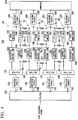
- FIG. 4 is a circuit diagram showing an example of the constitution of the high frequency signal amplifying apparatus 100 of the embodiment.
- the high frequency signal amplifying apparatus 100 includes a splitter 102, a plurality of Doherty amplifiers 1A, 1B, 1C, and 1D, a combiner 104, loop oscillation suppressors Rc-1, Rc-2, Rc-3, Rc-11, Rc-12, and Rc-13, and loop oscillation suppressors Rp-1, Rp-2, and Rp-3.
- the plurality of Doherty amplifiers 1A to 1D are connected in parallel with the splitter 102 and the combiner 104.
- the high frequency signal amplifying apparatus 100 includes the four Doherty amplifiers 1A to 1D within a single package.
- the splitter 102, the Doherty amplifiers 1A to 1D, and the combiner 104 are formed planarly. If no distinction is to be made between the loop oscillation suppressors Rc-1, Rc-2, Rc-3, Rc-11, Rc-12, and Rc-13 and other loop oscillation suppressors, the hyphens and the numbers that follow will be omitted, and if no distinction is to be made between the loop oscillation suppressors Rp-1, Rp-2 and Rp-3 and other loop oscillation suppressors, the hyphens and the numbers that follow will be omitted.
- the high frequency signal amplifying apparatus 100 of the embodiment includes four Doherty amplifiers 1 that are connected in parallel, the number four is not a restriction.
- the plurality of Doherty amplifiers 1A to 1D are disposed so that amplifiers of the same type neighbor each other.
- the disposition is such that the carrier amplifier 20A of the Doherty amplifier 1A and the carrier amplifier 20B of the Doherty amplifier 1B are mutually neighboring, and such that the peak amplifier 18B of the Doherty amplifier 1B and the peak amplifier 18C of the Doherty amplifier 1C are mutually neighboring.
- the disposition is such that the carrier amplifier 20C of the Doherty amplifier 1C and the carrier amplifier 20D of the Doherty amplifier 1D are mutually neighboring.
- the loop oscillation suppressors Rc-1 and Rc-2 are located between the carrier amplifier 20A and the carrier amplifier 20B.
- the loop oscillation suppressor Rc-1 is located between the signal input terminal of the carrier amplifier 20A and the signal input terminal of the carrier amplifier 20B.
- the loop oscillation suppressor Rc-2 is located between the signal output terminal of the carrier amplifier 20A and the signal output terminal of the carrier amplifier 20B.
- the loop oscillation suppressor Rc-3 is located between the signal output terminal of the ⁇ /4 line 32A and the signal output terminal of the ⁇ /4 line 32B.
- the loop oscillation suppressors Rc-1 and Rc-2 may be disposed between the carrier amplifier 20A and the carrier amplifier 20B.
- the loop oscillation suppressors Rc-1 and Rc-2 may be electrically connected between the carrier amplifier 20A and the carrier amplifier 20B.
- the loop oscillation suppressor Rc-3 may be disposed between the signal output terminal of the ⁇ /4 line 32A and the signal output terminal of the ⁇ /4 line 32B.
- the loop oscillation suppressor Rc-3 may be electrically connected between the signal output terminal of the ⁇ /4 line 32A and the signal output terminal of the ⁇ /4 line 32B.
- the loop oscillation suppressors Rp-2 and Rp-3 are located between the peak amplifier 18B and the peak amplifier 18C.
- the loop oscillation suppressor Rp-2 is located between the signal input terminal of the peak amplifier 18B and the signal input terminal of the peak amplifier 18C.
- the loop oscillation suppressor Rp-3 is located between the signal output terminal of the peak amplifier 18B and the signal output terminal of the peak amplifier 18C.
- the loop oscillation suppressor Rp-1 is located between the signal input terminal of the divided constant line 30B and the signal input terminal of the divided constant line 30C.
- the loop oscillation suppressors Rp-2 and Rp-3 may be disposed between the peak amplifier 18B and the peak amplifier 18C.
- the loop oscillation suppressors Rp-2 and Rp-3 may be electrically connected between the peak amplifier 18B and the peak amplifier 18C.
- the loop oscillation suppressor Rp-1 may be disposed between the signal input terminal of the divided constant line 30B and the signal input terminal of the divided constant line 30C.
- the loop oscillation suppressor Rp-1 may be electrically connected between the signal input terminal of the divided constant line 30B and the signal input terminal of the divided constant line 30C.
- the loop oscillation suppressors Rc-11 and Rc-12 are located between the carrier amplifier 20C and the carrier amplifier 20D.
- the loop oscillation suppressor Rc-11 is located between the signal input terminal of the carrier amplifier 20C and the signal input terminal of the carrier amplifier 20D
- the loop oscillation suppressor Rc-12 is located between the signal output terminal of the carrier amplifier 20C and the signal output terminal of the carrier amplifier 20D.
- the loop oscillation suppressor Rc-13 is located between the signal output terminal of the ⁇ /4 line 32C and the signal output terminal of the ⁇ /4 line 32D.
- the loop oscillation suppressors Rc-11 and Rc-12 may be disposed between the carrier amplifier 20C and the carrier amplifier 20D.
- the loop oscillation suppressors Rc-11 and Rc-12 may be electrically connected between the carrier amplifier 20C and the carrier amplifier 20D.
- the loop oscillation suppressor Rc-13 may be disposed between the signal output terminal of the ⁇ /4 line 32C and the signal output terminal of the ⁇ /4 line 32D.
- the loop oscillation suppressor Rc-13 may be electrically connected between the signal output terminal of the ⁇ /4 line 32C and the signal output terminal of the ⁇ /4 line 32D.
- the loop oscillation suppressor Rc-1 for example, is located between locations of the input side of the carrier amplifier 20A and the input side of the carrier amplifier 20B, which should be at the same potential, and has a resistance value.
- the resistance value for example, includes a resistance value of a resistor in addition to the resistance of the interconnection (and the same applies below).
- the loop oscillation suppressor Rc-2 is c located between locations of the output side of the carrier amplifier 20A and the output side of the carrier amplifier 20B, which should be at the same potential, and has a resistance value.
- the loop oscillation suppressor Rc-3, the loop oscillation suppressors Rp-1, Rp-2, and Rp-3, and the loop oscillation suppressors Rc-11, Rc-12, and Rc-13 also locates interconnections that should be at the same potential and have resistance values.
- positions midway in the matching circuit 12, the divided constant line 30, the peak amplifier 18, the carrier amplifier 20, the ⁇ /4 line 32, and the matching circuit 26 that should be at the same potential may be connected (and the same applies below).
- the resistance values of each of the loop oscillation suppressors may be mutually different values by optimization.
- loop oscillation might occur in this type of high frequency signal amplifying apparatus. Even if there is no RF input power, this oscillation phenomenon can grow from of thermal noise power, or can occur by a high power input at a specific frequency, and can affect the operation of the amplifier.
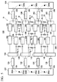
- FIG. 5 describes the loop oscillation paths in the high frequency signal amplifying apparatus 100 of the embodiment.
- the high frequency signal amplifying apparatus 100 includes the loop oscillation paths 200A, 200B, and 200C when the carrier amplifiers 20 and the peak amplifiers 18 are operating.
- the loop oscillation paths 200A, 200B, and 200C are linked and formed by the node points 200a and 200b in the splitter 102 and the combiner 104, respectively.
- the loop oscillation path 200A is formed by the carrier amplifier 20A, the ⁇ /4 line 32A, the matching circuit 26A, the combiner 104, the matching circuit 26B, the ⁇ /4 line 32B, the carrier amplifier 20B, the splitter 14B, the matching circuit 12B, the splitter 102, the matching circuit 12A, and the splitter 14A, and by the signal lines connecting these.
- the loop oscillation path 200B is formed by the peak amplifier 18B, the matching circuit 26B, the combiner 104, the matching circuit 26C, the peak amplifier 18C, the divided constant line 30C, the splitter 14C, the matching circuit 12C, the splitter 102, the matching circuit 12B, and the divided constant line 30B, and by the signal lines connecting these.
- the loop oscillation path 200C is formed by the carrier amplifier 20C, the ⁇ /4 line 32C, the matching circuit 26C, the combiner 104, the matching circuit 26D, the ⁇ /4 line 32D, the carrier amplifier 20D, the splitter 14D, the matching circuit 12D, the splitter 102, the matching circuit 12C, and the splitter 14C, and by the signal lines connecting these.
- FIG. 6 describes the loop oscillation paths in the high frequency signal amplifying apparatus 100 of the embodiment.
- the grouping of the path from the matching circuit 12A up to the matching circuit 26A and the path from the matching circuit 12B up to the matching circuit 26B and the grouping of the path from the matching circuit 12C up to the matching circuit 26C and the path from the matching circuit 12D up to the matching circuit 26D are joined at the node points 300a and 300b of the splitter 102 and the combiner 104, respectively, thereby forming the loop oscillation path 300.
- the high frequency signal amplifying apparatus 100 of the embodiment in order to suppress loop oscillation, peak amplifiers 18 or carrier amplifiers 20 are located so as to neighbor each other, and the loop oscillation suppressors Rc and Rp having resistance values are provided so as to suppress loop oscillation between the amplifiers.
- the high frequency signal amplifying apparatus 100 may be a monolithic microwave integrated circuit formed on a single substrate.
- the monolithic microwave integrated circuit may be housed in a package.
- the loop oscillation suppressors Rc-1, Rc-2, and Rc-3 can suppress loop oscillation occurring in the loop oscillation path 200A.
- the loop oscillation suppressors Rc-11, Rc-12, and Rc-13 can suppress loop oscillation occurring in the loop oscillation path 200C.
- the loop oscillation suppressor Rp-1, Rp-2, and Rp-3 can suppress loop oscillation occurring in the loop oscillation path 200B when the peak amplifier 18B or the peak amplifier 18C is operating.
- the loop oscillation suppressor Rc-3 can suppress loop oscillation occurring in the loop oscillation path 300.
- the parasitic inductance of the loop oscillation suppressors locating between neighboring carrier amplifiers 20 or between neighboring peak amplifiers 18 can be made small.
- the loop oscillation suppressors are therefore substantially only resistors, enabling suppression of loop oscillation without almost no dependence on frequency. Described another way, amplifiers of the same type, which should be at the same potential, are caused to neighbor each other in order to suppress the occurrence of loop oscillation over a broad frequency band.
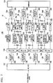
- FIG. 7 is a circuit diagram showing an example of another constitution of the high frequency signal amplifying apparatus 100 of the embodiment.
- This high frequency signal amplifying apparatus 100 causes the peak amplifier 18A of the Doherty amplifier 1A and the peak amplifier 18B of the Doherty amplifier 1B to neighbor each other, causes the carrier amplifier 20B of the Doherty amplifier 1B and the carrier amplifier 20C of the Doherty amplifier 1C to neighbor each other, and causes the peak amplifier 18C of the Doherty amplifier 1C and the peak amplifier 18D of the Doherty amplifier 1D to neighbor each other.
- loop oscillation suppressors Rp-11, Rp-12, and Rp-13 are located between the peak amplifier 18A and the peak amplifier 18B
- loop oscillation suppressors Rc-21, Rc-22, and Rc-23 are located between the carrier amplifier 20B and the carrier amplifier 20C
- loop oscillation suppressors Rp-21, Rp-22, and Rp-23 are located between the peak amplifier 18C and the peak amplifier 18D.
- the loop oscillation suppressors Rp-11, Rp-12, and Rp-13 may be disposed between the peak amplifier 18A and the peak amplifier 18B.
- the loop oscillation suppressors Rp-11, Rp-12, and Rp-13 may be electrically connected between the peak amplifier 18A and the peak amplifier 18B.
- the loop oscillation suppressors Rc-21, Rc-22, and Rc-23 may be disposed between the carrier amplifier 20B and the carrier amplifier 20C.
- the loop oscillation suppressors Rc-21, Rc-22, and Rc-23 may be electrically connected between the carrier amplifier 20B and the carrier amplifier 20C.
- the loop oscillation suppressors Rp-21, Rp-22, and Rp-23 may be disposed between the peak amplifier 18C and the peak amplifier 18D.
- the loop oscillation suppressors Rp-21, Rp-22, and Rp-23 may be electrically connected between the peak amplifier 18C and the peak amplifier 18D.
- FIG. 8 describes the loop oscillation paths in the high frequency signal amplifying apparatus 100 of the embodiment.
- the high frequency signal amplifying apparatus 100 includes the loop oscillation paths 400A, 400B, and 400C when the peak amplifiers 18 and the carrier amplifiers 20 are operating.
- the loop oscillation paths 400A, 400B, and 400C are formed by joining at the node points 400a and 400b in the splitter 102 and the combiner 104, respectively.
- the loop oscillation path 400A is formed by the peak amplifier 18A, the matching circuit 26A, the combiner 104, the matching circuit 26B, the peak amplifier 18B, the divided constant line 30B, the splitter 14B, the matching circuit 12B, the splitter 102, the matching circuit 12A, the splitter 14A, and the divided constant line 30A, and by the signal lines that connect these.
- the loop oscillation path 400B is formed by the carrier amplifier 20B, the ⁇ /4 line 32B, the matching circuit 26B, the combiner 104, the matching circuit 26C, the ⁇ /4 line 32C, the carrier amplifier 20C, the splitter 14C, the matching circuit 12C, the splitter 102, and the matching circuit 12B, and by the splitter 14B, and by the signal lines that connect these.
- the loop oscillation path 400C is formed by the peak amplifier 18C, the matching circuit 26C, the combiner 104, the matching circuit 26D, the peak amplifier 18D, the divided constant line 30D, the splitter 14D, the matching circuit 12D, the splitter 102, the matching circuit 12C, the splitter 14C, and the divided constant line 30C, and by the signal lines that connect these.
- FIG. 9 describes the loop oscillation paths in the high frequency signal amplifying apparatus 100 of the embodiment.
- the grouping of the path from the matching circuit 12A up to the matching circuit 26A and the path from the matching circuit 12B up to the matching circuit 26B and the grouping of the path from the matching circuit 12C up to the matching circuit 26C and the path from the matching circuit 12D up to the matching circuit 26D are joined at the node points 500a and 500b, of the splitter 102 and the combiner 104, respectively, thereby forming the loop oscillation path 500.
- the loop oscillation suppressors Rp-11, Rp-12, and Rp-13 can suppress loop oscillation occurring in the loop oscillation path 400A.
- the loop oscillation suppressors Rp-21, Rp-22, and Rr-23 can suppress loop oscillation occurring in the loop oscillation path 400C
- the loop oscillation suppressors Rc-21, Rc-22, and Rc-23 can suppress loop oscillation occurring in the loop oscillation path 400B
- the loop oscillation suppressor Rc-23 can suppress loop oscillation occurring in the loop oscillation path 500.
- the high frequency signal amplifying apparatus 100 of the embodiment described above enables a constitution in which the peak amplifiers 18 of the plurality of respective Doherty amplifiers 1 or the carrier amplifiers 20 of the plurality of respective Doherty amplifiers 1 are caused to be mutually neighboring, because there are loop oscillation suppressors located between the neighboring peak amplifiers 18 or the carrier amplifiers 20, the conditions for loop oscillations are not satisfied.
- the embodiment enables suppression of loop oscillation between the plurality of Doherty amplifiers 1.
- a constitution can be adopted in which, when loop oscillation tends to occur between the carrier amplifiers 20, which operate for a longer period of time than do the peak amplifiers 18, the carrier amplifiers 20 are disposed as to be neighboring, such as shown in FIG. 4 , and, conversely, when loop oscillation tends to occur between the peak amplifiers 18, the peak amplifiers 18, which have high non-linearity, are disposed so as to be neighboring, such as shown in FIG. 7 , thereby enabling avoiding satisfying the condition of the respective loop oscillations.
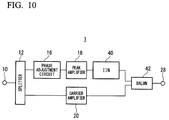
- FIG. 10 is a block diagram showing the constitution of a variation example of the Doherty amplifier 1 in the high frequency signal amplifying apparatus 100 of the embodiment, this block diagram showing a series- connected load type Doherty amplifier 1.
- the Doherty amplifier 1, as shown in FIG. 10 includes an IIN (impedance inverting network) 40 and a balun 42.
- the balun 42 is a converter that converts a high frequency signal between the balanced line and an unbalanced line and is, for example, a converter, one end of which is connected to the IIN 40 and the carrier amplifier 20, and the other end of which is connected to the output terminal 28.
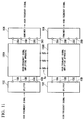
- FIG. 11 is a block diagram showing the constitution of an application example of the high frequency signal amplifying apparatus 100 of the embodiment.
- the high frequency signal amplifying apparatus of the application example includes a high frequency signal amplifying apparatus 100A and a high frequency signal amplifying apparatus 100B, which include the same constitution as the above-described high frequency signal amplifying apparatus 100, disposed in parallel, with loop oscillation suppressors Rc located between the high frequency signal amplifying apparatus 100A and the high frequency signal amplifying apparatus 100B.
- the loop oscillation suppressors Rc may be disposed between the high frequency signal amplifying apparatus 100A and the high frequency signal amplifying apparatus 100B.
- the loop oscillation suppressors Rc may be electrically connected between the high frequency signal amplifying apparatus 100A and the high frequency signal amplifying apparatus 100B.
- the high frequency signal amplifying apparatus 100A and the high frequency signal amplifying apparatus 100B may be a monolithic microwave integrated circuit formed on a single substrate.
- the monolithic microwave integrated circuit may be housed in a package.
- the amplifiers included in the high frequency signal amplifying apparatus 100A and the amplifiers included in the high frequency signal amplifying apparatus 100B are disposed so that amplifiers of the same type neighbor each other.
- the loop oscillation suppressors Rc locate, for example, the input side of the carrier amplifiers 20A with the input side of the carrier amplifiers 20B, which should be at the same potential, and have a resistance value.
- the loop oscillation suppressors Rc also locate, for example, the output side of the carrier amplifiers 20A with the output side of the carrier amplifiers 20B, which should be at the same potential, and have a resistance value.
- the embodiment enables the suppression of the occurrence of loop oscillation in the high frequency signal amplifying apparatus 100.
- FIG. 12 is a circuit diagram of a high frequency signal amplifying apparatus of the comparison example.
- the high frequency signal amplifying apparatus of the comparison example disposes two Doherty amplifiers so that peak amplifiers are not neighboring each other and so that carrier amplifiers are not neighboring each other.
- resistors R are connected between the input terminals of the peak amplifiers and between the output terminals of the peak amplifiers, it is necessary to form interconnections that straddle across a ⁇ /4 line.
- the required length of the lines for providing the resistors R become long, and there is a possibility that the inductance of the lines increases.
- the resistors R are provided, there is a possibility that the effect of suppressing loop oscillation will be reduced, relative to the high frequency signal amplifying apparatus 100 of the embodiment.
- the high frequency signal amplifying apparatus 100 of the embodiments described above has been described with regard to a constitution in which a plurality of parallel-connected Doherty amplifiers 1 are disposed, the constitution disclosed in the embodiment can also be applied to a constitution in which a plurality of series-connected Doherty amplifiers 1 are disposed. That is, in addition to disposing a plurality of Doherty amplifiers 1 in series, amplifiers of the same type are caused to neighbor each other. In a series-connected type Doherty amplifier 1, loop oscillation suppressors Rc are located between neighboring amplifiers of the same type. These loop oscillation suppressors Rc are located so as to connect locations in amplifiers of the same type that should be at the same potential. As a result, the high frequency signal amplifying apparatus 100 of the embodiment can suppress the occurrence of loop oscillation even if the Doherty amplifiers 1 are of the series-connected type.
Landscapes
- Engineering & Computer Science (AREA)
- Power Engineering (AREA)
- Microelectronics & Electronic Packaging (AREA)
- Amplifiers (AREA)
Abstract
Description
- This application is based upon and claims the benefit of priority from
Japanese Patent Application No. 2015-003564, filed January 9, 2015 - Embodiments described herein relate generally to a high-frequency signal amplifying circuitry.
- A Doherty amplifier that efficiently amplifies a backed-off high frequency signal has been known. A Doherty amplifier includes a carrier amplifier and a peak amplifier connected in parallel and combines and outputs the high frequency signals amplified by the carrier amplifier and the peak amplifier. There are cases in which a Doherty amplifier is connected in parallel with another Doherty amplifier, the same signal being divided to and amplified by the Doherty amplifier as the other Doherty amplifier. In this case, depending upon the circuit conditions, loop oscillation might occur between the Doherty amplifiers.
-
-
FIG. 1 is a block diagram showing the constitution of a Doherty amplifier in a high frequency signal amplifying apparatus of an embodiment. -
FIG. 2 is a block diagram for the case in which, in the Doherty amplifier-of the embodiment, a divided constant line is used as an example of the constitution of a phase adjustment circuit and a λ/4 line is used as an example of the constitution of an impedance inverting network (IIN). -
FIG. 3 shows an example of the relationship between the input power and the output power of the Doherty amplifier of the embodiment. -
FIG. 4 is a circuit diagram showing an example of the constitution of high frequency signal amplifying apparatus of the embodiment. -
FIG. 5 is a drawing describing the loop oscillation paths in the high frequency signal amplifying apparatus of the embodiment. -
FIG. 6 is a drawing describing the loop oscillation paths in the high frequency signal amplifying apparatus of the embodiment. -
FIG. 7 is a circuit diagram showing an example of another constitution of the high frequency signal amplifying apparatus of the embodiment. -
FIG. 8 is drawing describing the loop oscillation paths in the high frequency signal amplifying apparatus of the embodiment. -
FIG. 9 is drawing describing the loop oscillation paths in the high frequency signal amplifying apparatus of the embodiment. -
FIG. 10 is a block diagram showing the constitution of a variation example of the Dohertyamplifier 1 in the high frequency signal amplifying apparatus of the embodiment. -
FIG. 11 is a block diagram showing the constitution of an application example of the high frequency signal amplifying apparatus of the embodiment. -
FIG. 12 is a drawing showing a high frequency signal amplifying apparatus of a comparison example. - Some embodiments are directed to a high frequency signal amplifying circuitry. The high frequency signal amplifying circuitry may include, but is not limited to, a first splitter, a first amplifier, a second amplifier, and a first loop oscillation suppressor. The first amplifier includes a second splitter that divides a signal supplied from the first splitter, a first carrier amplifier, a first peak amplifier, and a first combiner that combines signals output from the first carrier amplifier and from the first peak amplifier. The second amplifier-includes a third splitter that divides a signal supplied from the first splitter, a second carrier amplifier, a second peak amplifier, and a second combiner that combines signals output from the second carrier amplifier and from the second peak amplifier. The second carrier amplifier is adjacent to an associated the first carrier amplifier or the second peak amplifier is adjacent to an associated the first peak amplifier. The first loop oscillation suppressor locates between the second carrier amplifier and the associated first carrier amplifier or the second peak amplifier and the associated first peak amplifier. The third combiner combines signals output from the first combiner and the second combiner.
- The first loop oscillation suppressor may be disposed between the second carrier amplifier and the associated first carrier amplifier or the second peak amplifier and the associated first peak amplifier. The first loop oscillation suppressor may be electrically connected between the second carrier amplifier and the associated first carrier amplifier or the second peak amplifier and the associated first peak amplifier.
- In some embodiments, the first loop oscillation suppressor may connect between locations of the second carrier amplifier and the associated first carrier amplifier or the second peak amplifier and the associated first peak amplifier.
- In some embodiments, the first loop oscillation suppressor connects either first and second nodes or third and fourth nodes. The first and second nodes are inputs of the first and second amplifiers, respectively. The third and fourth nodes are outputs of the first and second amplifiers, respectively.
- In other words, the first and second nodes are inputs of the first and second amplifiers, respectively, and the first and second nodes are to have a first potential. In other words, the third and fourth nodes are outputs of the first and second amplifiers, respectively, and the third and fourth nodes are to have a second potential which is different from the first potential.
- In some embodiments, the first loop oscillation suppressor includes a resistor.
- In some embodiments, the high frequency signal amplifying circuitry may include, but is not limited to, a second loop oscillation suppressor; a third amplifier; and a fourth amplifier. The third amplifier includes a fourth splitter that divides a signal supplied from the first splitter, a third carrier amplifier, a third peak amplifier, and a fourth combiner that combines signals output from the third carrier amplifier and from the third peak amplifier. The fourth amplifier-includes a fifth splitter that divides a signal supplied from the first splitter, a fourth carrier amplifier, a fourth peak amplifier, and a fifth combiner that combines signals output from the fourth carrier amplifier and from the fourth peak amplifier. The fourth carrier amplifier is adjacent to an associated the third carrier amplifier or the fourth peak amplifier is adjacent to an associated the third peak amplifier. The third combiner combines signals output from the first combiner, the second combiner, the fourth combiner and the fifth combiner. A first pair of the first and second amplifiers is adjacent to a second pair of the third and fourth amplifiers. The second loop oscillation suppressor locates between the fourth carrier amplifier and the associated third carrier amplifier or the fourth peak amplifier and the associated third peak amplifier.
- The third loop oscillation suppressor may located between the first pair of the first and second amplifiers and the second pair of the third and fourth amplifiers.
- In some embodiments, at least one of the first carrier amplifier, the first peak amplifier, the second carrier amplifier, the second peak amplifier, the second splitter, the third splitter, the first combiner, the second combiner, the first splitter, the third combiner, and the first loop oscillation suppressor is in a single package.
- In some embodiments, the circuitry may include, but is not limited to, a monolithic microwave integrated circuit (MIMIC) on a single semiconductor substrate. The MMIC includes a part of a group consisting of: at least a part of the first carrier amplifier, at least a part of the first peak amplifier, at least a part of the second carrier amplifier, at least a part of the second peak amplifier, at least a part of the second splitter, at least a part of the third splitter, at least a part of the first combiner, at least a part of the second combiner, at least a part of the first splitter, at least a part of the third combiner, and at least a part of the first loop oscillation suppressor..
- The high frequency signal amplifying apparatus of an embodiment will be described below, with references made to the drawings.
- First, the Doherty amplifiers included in the high frequency signal amplifying apparatus of the embodiment will be described.
FIG. 1 is a block diagram showing the constitution of a parallel-connected load type Dohertyamplifier 1 in a high frequency signal amplifying apparatus of the embodiment. The Dohertyamplifier 1 is inputted a high frequency signal and outputs an amplified high frequency signal to a non-illustrated antenna. - The Doherty
amplifier 1 includes aninput terminal 10, amatching circuit 12, asplitting unit 14, aphase adjustment circuit 16, apeak amplifier 18, acarrier amplifier 20, an IIN (impedance inverting network) 22, a combiningunit 24, amatching circuit 26, and anoutput terminal 28. - A high frequency signal is supplied to the
input terminal 10 as the input signal. A high frequency signal is a signal, for example, in the RF (radio frequency) band. The high frequency signal supplied to theinput terminal 10 is sent to the matchingcircuit 12. - The matching
circuit 12 and thematching circuit 26 match the input impedance and the output impedance of the Dohertyamplifier 1. The matchingcircuit 12 and thematching circuit 26 include circuits that are combinations of inductors and capacitors formed on a substrate. Alternatively, thematching circuit 12 and thematching circuit 26 may be constituted by not only inductors and capacitors, but also resistors that are formed on the substrate. - The
splitting unit 14 is connected to theinput terminal 10 via thematching circuit 12 and divides the high frequency signal to thecarrier amplifier 20 and thepeak amplifier 18. - The
phase adjustment circuit 16 between thesplitting unit 14 and thepeak amplifier 18 adjusts the phase of the high frequency signal divided from thesplitting unit 14 so that thepeak amplifier 18 and thecarrier amplifier 20 are in phase with each other at the splittingunit 14.FIG. 2 is a block diagram showing, in the Dohertyamplifier 1 of the embodiment, the case in which a dividedconstant line 30 is used as an example of the constitution of thephase adjustment circuit 16. The high frequency signal that has passed through the dividedconstant line 30 is supplied to thepeak amplifier 18. The high frequency signal that has been amplified by thepeak amplifier 18 is supplied to the combiningunit 24. - The
IIN 22 inverts the impedance between thecarrier amplifier 20 and the combiningunit 24. As shown inFIG. 2 , theIIN 22 includes a λ/4 line (1/4 wavelength)line 32. The λ/4line 32 inverts the impedance and also delays the phase of the input signal by 90°. The high frequency signal that has passed through the λ/4line 32 is supplied to the combiningunit 24. - The combining
unit 24 combines the high frequency signal supplied from thepeak amplifier 18 and the high frequency signal supplied from theIIN 22. The high frequency signal combined by the combiningunit 24 is supplied to thematching circuit 26. The high frequency signal that has passed through the matchingcircuit 26 is output from theoutput terminal 28 as the output signal. - The
carrier amplifier 20 is an amplifier that uses, for example, an FET (field effect transistor) having a gate bias voltage applied thereto so that it operates as an class AB amplifier or a class B amplifier. Thepeak amplifier 18 is an amplifier that uses, for example. An FET (field effect transistor) having a gate bias voltage applied thereto so that it operates as a class C amplifier. -
FIG. 3 shows an example of the relationship between the input power and the output power in theDoherty amplifier 1 of the embodiment. In thecarrier amplifier 20, the gate bias voltage is set to substantially pinch it off, and amplification is done from a high frequency signal with small amplitude. When the input power to thecarrier amplifier 20 is below a prescribed power P1, thecarrier amplifier 20 amplifies linearly and outputs the output power Pc. When the input power to thecarrier amplifier 20 approaches the prescribed power P1 and the output power Pc exceeds P3, saturation begins. - The gate bias voltage in the
peak amplifier 18 is set more deeply than thecarrier amplifier 20 and starts amplification operation when a high frequency signal having an amplitude (power value) exceeding a prescribed value is supplied. Thepeak amplifier 18 starts operating, for example, when theDoherty amplifier 1 is backed off 5 dB from the saturation power. This backoff is the ratio between the average output power and the saturation output power of theDoherty amplifier 1. - The
peak amplifier 18, as shown inFIG. 3 , goes into the off state when the input power is lower than the prescribed power P1. In thepeak amplifier 18, when the input power exceeds the prescribed power P1, a period of time in which the gate opens occurs, and the high frequency signal is amplified. When the input power is higher than the prescribed power P1, thepeak amplifier 18 can amplify the input power to the output signal Pp. - In the above-noted
Doherty amplifier 1, thecarrier amplifier 20 amplifies a high frequency signal of relatively small power, and is set so that when thecarrier amplifier 20 voltage begins to saturate, thepeak amplifier 18 goes into the on state. Thepeak amplifier 18 operates so as to compensate for the amount of gain lost because of saturation of thecarrier amplifier 20 voltage. This enables theDoherty amplifier 1 to amplify linearly and output the output power Pd until the input power reaches P2, as shown by the dotted line inFIG. 3 . - It is desirable that the
peak amplifier 18 and thecarrier amplifier 20 are internally matched field effect transistor amplifiers in which impedance matching is done within the package. Alternatively, thepeak amplifier 18 and thecarrier amplifier 20 may use discrete semiconductors as the field effect transistors. According to theDoherty amplifier 1, it is possible to achieve the optimum signal source impedance and optimum load impedance at the input electrode and the output electrode of the field effect transistor chip of thepeak amplifier 18 and thecarrier amplifier 20, enabling efficient amplification operation. - Also, according to the
Doherty amplifier 1 of the embodiment, a constitution may be adopted in which thepeak amplifier 18, thecarrier amplifier 20, the splittingunit 14, the combiningunit 24, thephase adjustment circuit 16, and theIIN 22 are included in a single monolithic microwave integrated circuit (MMIC). - A high frequency
signal amplifying apparatus 100 having a plurality of the Doherty amplifier as noted above will be described, with reference made toFIG. 4 . -
FIG. 4 is a circuit diagram showing an example of the constitution of the high frequencysignal amplifying apparatus 100 of the embodiment. - The high frequency
signal amplifying apparatus 100 includes asplitter 102, a plurality ofDoherty amplifiers combiner 104, loop oscillation suppressors Rc-1, Rc-2, Rc-3, Rc-11, Rc-12, and Rc-13, and loop oscillation suppressors Rp-1, Rp-2, and Rp-3. In the high frequencysignal amplifying apparatus 100, the plurality ofDoherty amplifiers 1A to 1D are connected in parallel with thesplitter 102 and thecombiner 104. The high frequencysignal amplifying apparatus 100 includes the fourDoherty amplifiers 1A to 1D within a single package. In the high frequencysignal amplifying apparatus 100, thesplitter 102, theDoherty amplifiers 1A to 1D, and thecombiner 104 are formed planarly. If no distinction is to be made between the loop oscillation suppressors Rc-1, Rc-2, Rc-3, Rc-11, Rc-12, and Rc-13 and other loop oscillation suppressors, the hyphens and the numbers that follow will be omitted, and if no distinction is to be made between the loop oscillation suppressors Rp-1, Rp-2 and Rp-3 and other loop oscillation suppressors, the hyphens and the numbers that follow will be omitted. - Although the high frequency
signal amplifying apparatus 100 of the embodiment includes fourDoherty amplifiers 1 that are connected in parallel, the number four is not a restriction. The number of plurality ofDoherty amplifiers 1 is a number thereof that are connected in parallel in response to a power value requested by the high frequencysignal amplifying apparatus 100. For example, if the output of oneDoherty amplifier 1 is 50 W and the requested power is 400 W, eightDoherty amplifiers 1 may be connected in parallel, and, for example, 2n (where n= 1, 2, 3, ...)Doherty amplifiers 1 may be connected in parallel. Alternatively, an arbitrary number N (N=2, 3, 4,...)Doherty amplifiers 1 may be connected in parallel. - The plurality of
Doherty amplifiers 1A to 1D are disposed so that amplifiers of the same type neighbor each other. In the high frequencysignal amplifying apparatus 100 shown inFIG. 4 , the disposition is such that thecarrier amplifier 20A of theDoherty amplifier 1A and thecarrier amplifier 20B of theDoherty amplifier 1B are mutually neighboring, and such that thepeak amplifier 18B of theDoherty amplifier 1B and thepeak amplifier 18C of theDoherty amplifier 1C are mutually neighboring. Also, the disposition is such that thecarrier amplifier 20C of theDoherty amplifier 1C and thecarrier amplifier 20D of theDoherty amplifier 1D are mutually neighboring. - In the high frequency
signal amplifying apparatus 100, the loop oscillation suppressors Rc-1 and Rc-2 are located between thecarrier amplifier 20A and thecarrier amplifier 20B. The loop oscillation suppressor Rc-1 is located between the signal input terminal of thecarrier amplifier 20A and the signal input terminal of thecarrier amplifier 20B. The loop oscillation suppressor Rc-2 is located between the signal output terminal of thecarrier amplifier 20A and the signal output terminal of thecarrier amplifier 20B. The loop oscillation suppressor Rc-3 is located between the signal output terminal of the λ/4line 32A and the signal output terminal of the λ/4line 32B. - The loop oscillation suppressors Rc-1 and Rc-2 may be disposed between the
carrier amplifier 20A and thecarrier amplifier 20B. The loop oscillation suppressors Rc-1 and Rc-2 may be electrically connected between thecarrier amplifier 20A and thecarrier amplifier 20B. The loop oscillation suppressor Rc-3 may be disposed between the signal output terminal of the λ/4line 32A and the signal output terminal of the λ/4line 32B. The loop oscillation suppressor Rc-3 may be electrically connected between the signal output terminal of the λ/4line 32A and the signal output terminal of the λ/4line 32B. - The loop oscillation suppressors Rp-2 and Rp-3 are located between the
peak amplifier 18B and thepeak amplifier 18C. The loop oscillation suppressor Rp-2 is located between the signal input terminal of thepeak amplifier 18B and the signal input terminal of thepeak amplifier 18C. The loop oscillation suppressor Rp-3 is located between the signal output terminal of thepeak amplifier 18B and the signal output terminal of thepeak amplifier 18C. The loop oscillation suppressor Rp-1 is located between the signal input terminal of the dividedconstant line 30B and the signal input terminal of the dividedconstant line 30C. - The loop oscillation suppressors Rp-2 and Rp-3 may be disposed between the
peak amplifier 18B and thepeak amplifier 18C. The loop oscillation suppressors Rp-2 and Rp-3 may be electrically connected between thepeak amplifier 18B and thepeak amplifier 18C. The loop oscillation suppressor Rp-1 may be disposed between the signal input terminal of the dividedconstant line 30B and the signal input terminal of the dividedconstant line 30C. The loop oscillation suppressor Rp-1 may be electrically connected between the signal input terminal of the dividedconstant line 30B and the signal input terminal of the dividedconstant line 30C. - The loop oscillation suppressors Rc-11 and Rc-12 are located between the
carrier amplifier 20C and thecarrier amplifier 20D. The loop oscillation suppressor Rc-11 is located between the signal input terminal of thecarrier amplifier 20C and the signal input terminal of thecarrier amplifier 20D, and the loop oscillation suppressor Rc-12 is located between the signal output terminal of thecarrier amplifier 20C and the signal output terminal of thecarrier amplifier 20D. The loop oscillation suppressor Rc-13 is located between the signal output terminal of the λ/4line 32C and the signal output terminal of the λ/4line 32D. - The loop oscillation suppressors Rc-11 and Rc-12 may be disposed between the
carrier amplifier 20C and thecarrier amplifier 20D. The loop oscillation suppressors Rc-11 and Rc-12 may be electrically connected between thecarrier amplifier 20C and thecarrier amplifier 20D. The loop oscillation suppressor Rc-13 may be disposed between the signal output terminal of the λ/4line 32C and the signal output terminal of the λ/4line 32D. The loop oscillation suppressor Rc-13 may be electrically connected between the signal output terminal of the λ/4line 32C and the signal output terminal of the λ/4line 32D. - The loop oscillation suppressor Rc-1, for example, is located between locations of the input side of the
carrier amplifier 20A and the input side of thecarrier amplifier 20B, which should be at the same potential, and has a resistance value. The resistance value, for example, includes a resistance value of a resistor in addition to the resistance of the interconnection (and the same applies below). The loop oscillation suppressor Rc-2 is c located between locations of the output side of thecarrier amplifier 20A and the output side of thecarrier amplifier 20B, which should be at the same potential, and has a resistance value. In the same manner, the loop oscillation suppressor Rc-3, the loop oscillation suppressors Rp-1, Rp-2, and Rp-3, and the loop oscillation suppressors Rc-11, Rc-12, and Rc-13 also locates interconnections that should be at the same potential and have resistance values. Although it is not illustrated, positions midway in thematching circuit 12, the dividedconstant line 30, thepeak amplifier 18, thecarrier amplifier 20, the λ/4line 32, and thematching circuit 26 that should be at the same potential may be connected (and the same applies below). The resistance values of each of the loop oscillation suppressors may be mutually different values by optimization. - In general, loop oscillation might occur in this type of high frequency signal amplifying apparatus. Even if there is no RF input power, this oscillation phenomenon can grow from of thermal noise power, or can occur by a high power input at a specific frequency, and can affect the operation of the amplifier.
-
FIG. 5 describes the loop oscillation paths in the high frequencysignal amplifying apparatus 100 of the embodiment. As shown inFIG. 5 , the high frequencysignal amplifying apparatus 100 includes theloop oscillation paths carrier amplifiers 20 and thepeak amplifiers 18 are operating. Theloop oscillation paths splitter 102 and thecombiner 104, respectively. Theloop oscillation path 200A is formed by thecarrier amplifier 20A, the λ/4line 32A, thematching circuit 26A, thecombiner 104, thematching circuit 26B, the λ/4line 32B, thecarrier amplifier 20B, thesplitter 14B, thematching circuit 12B, thesplitter 102, thematching circuit 12A, and thesplitter 14A, and by the signal lines connecting these. Theloop oscillation path 200B is formed by thepeak amplifier 18B, thematching circuit 26B, thecombiner 104, thematching circuit 26C, thepeak amplifier 18C, the dividedconstant line 30C, thesplitter 14C, thematching circuit 12C, thesplitter 102, thematching circuit 12B, and the dividedconstant line 30B, and by the signal lines connecting these. Theloop oscillation path 200C is formed by thecarrier amplifier 20C, the λ/4line 32C, thematching circuit 26C, thecombiner 104, thematching circuit 26D, the λ/4line 32D, thecarrier amplifier 20D, thesplitter 14D, thematching circuit 12D, thesplitter 102, thematching circuit 12C, and thesplitter 14C, and by the signal lines connecting these. -
FIG. 6 describes the loop oscillation paths in the high frequencysignal amplifying apparatus 100 of the embodiment. As shown inFIG. 6 , in the high frequencysignal amplifying apparatus 100, the grouping of the path from thematching circuit 12A up to thematching circuit 26A and the path from thematching circuit 12B up to thematching circuit 26B and the grouping of the path from thematching circuit 12C up to thematching circuit 26C and the path from thematching circuit 12D up to thematching circuit 26D are joined at the node points 300a and 300b of thesplitter 102 and thecombiner 104, respectively, thereby forming the loop oscillation path 300. - In contrast, in the high frequency
signal amplifying apparatus 100 of the embodiment, in order to suppress loop oscillation,peak amplifiers 18 orcarrier amplifiers 20 are located so as to neighbor each other, and the loop oscillation suppressors Rc and Rp having resistance values are provided so as to suppress loop oscillation between the amplifiers. This enables the high frequencysignal amplifying apparatus 100 to be constituted so that the conditions for loop oscillation are not satisfied, thereby suppressing the occurrence of loop oscillation betweenDoherty amplifiers 1. The high frequencysignal amplifying apparatus 100 may be a monolithic microwave integrated circuit formed on a single substrate. The monolithic microwave integrated circuit may be housed in a package. - The loop oscillation suppressors Rc-1, Rc-2, and Rc-3 can suppress loop oscillation occurring in the
loop oscillation path 200A. In the same manner, the loop oscillation suppressors Rc-11, Rc-12, and Rc-13 can suppress loop oscillation occurring in theloop oscillation path 200C. The loop oscillation suppressor Rp-1, Rp-2, and Rp-3 can suppress loop oscillation occurring in theloop oscillation path 200B when thepeak amplifier 18B or thepeak amplifier 18C is operating. The loop oscillation suppressor Rc-3 can suppress loop oscillation occurring in the loop oscillation path 300. - In this case, according to the high frequency
signal amplifying apparatus 100 of the embodiment, because the connected amplifier are next to one another, the parasitic inductance of the loop oscillation suppressors locating between neighboringcarrier amplifiers 20 or between neighboringpeak amplifiers 18 can be made small. The loop oscillation suppressors are therefore substantially only resistors, enabling suppression of loop oscillation without almost no dependence on frequency. Described another way, amplifiers of the same type, which should be at the same potential, are caused to neighbor each other in order to suppress the occurrence of loop oscillation over a broad frequency band. -
FIG. 7 is a circuit diagram showing an example of another constitution of the high frequencysignal amplifying apparatus 100 of the embodiment. This high frequencysignal amplifying apparatus 100 causes thepeak amplifier 18A of theDoherty amplifier 1A and thepeak amplifier 18B of theDoherty amplifier 1B to neighbor each other, causes thecarrier amplifier 20B of theDoherty amplifier 1B and thecarrier amplifier 20C of theDoherty amplifier 1C to neighbor each other, and causes thepeak amplifier 18C of theDoherty amplifier 1C and thepeak amplifier 18D of theDoherty amplifier 1D to neighbor each other. - In this high frequency
signal amplifying apparatus 100, loop oscillation suppressors Rp-11, Rp-12, and Rp-13 are located between thepeak amplifier 18A and thepeak amplifier 18B, loop oscillation suppressors Rc-21, Rc-22, and Rc-23 are located between thecarrier amplifier 20B and thecarrier amplifier 20C, and loop oscillation suppressors Rp-21, Rp-22, and Rp-23 are located between thepeak amplifier 18C and thepeak amplifier 18D. - The loop oscillation suppressors Rp-11, Rp-12, and Rp-13 may be disposed between the
peak amplifier 18A and thepeak amplifier 18B. The loop oscillation suppressors Rp-11, Rp-12, and Rp-13 may be electrically connected between thepeak amplifier 18A and thepeak amplifier 18B. - The loop oscillation suppressors Rc-21, Rc-22, and Rc-23 may be disposed between the
carrier amplifier 20B and thecarrier amplifier 20C. The loop oscillation suppressors Rc-21, Rc-22, and Rc-23 may be electrically connected between thecarrier amplifier 20B and thecarrier amplifier 20C. - The loop oscillation suppressors Rp-21, Rp-22, and Rp-23 may be disposed between the
peak amplifier 18C and thepeak amplifier 18D. The loop oscillation suppressors Rp-21, Rp-22, and Rp-23 may be electrically connected between thepeak amplifier 18C and thepeak amplifier 18D. -
FIG. 8 describes the loop oscillation paths in the high frequencysignal amplifying apparatus 100 of the embodiment. As shown inFIG. 8 , the high frequencysignal amplifying apparatus 100 includes theloop oscillation paths peak amplifiers 18 and thecarrier amplifiers 20 are operating. Theloop oscillation paths splitter 102 and thecombiner 104, respectively. Theloop oscillation path 400A is formed by thepeak amplifier 18A, thematching circuit 26A, thecombiner 104, thematching circuit 26B, thepeak amplifier 18B, the dividedconstant line 30B, thesplitter 14B, thematching circuit 12B, thesplitter 102, thematching circuit 12A, thesplitter 14A, and the dividedconstant line 30A, and by the signal lines that connect these. Theloop oscillation path 400B is formed by thecarrier amplifier 20B, the λ/4line 32B, thematching circuit 26B, thecombiner 104, thematching circuit 26C, the λ/4line 32C, thecarrier amplifier 20C, thesplitter 14C, thematching circuit 12C, thesplitter 102, and thematching circuit 12B, and by thesplitter 14B, and by the signal lines that connect these. Theloop oscillation path 400C is formed by thepeak amplifier 18C, thematching circuit 26C, thecombiner 104, thematching circuit 26D, thepeak amplifier 18D, the dividedconstant line 30D, thesplitter 14D, thematching circuit 12D, thesplitter 102, thematching circuit 12C, thesplitter 14C, and the dividedconstant line 30C, and by the signal lines that connect these. -
FIG. 9 describes the loop oscillation paths in the high frequencysignal amplifying apparatus 100 of the embodiment. In the high frequencysignal amplifying apparatus 100, as shown inFIG. 9 , the grouping of the path from thematching circuit 12A up to thematching circuit 26A and the path from thematching circuit 12B up to thematching circuit 26B and the grouping of the path from thematching circuit 12C up to thematching circuit 26C and the path from thematching circuit 12D up to thematching circuit 26D are joined at the node points 500a and 500b, of thesplitter 102 and thecombiner 104, respectively, thereby forming theloop oscillation path 500. - By the above-noted constitution, the loop oscillation suppressors Rp-11, Rp-12, and Rp-13 can suppress loop oscillation occurring in the
loop oscillation path 400A. In the same manner, the loop oscillation suppressors Rp-21, Rp-22, and Rr-23 can suppress loop oscillation occurring in theloop oscillation path 400C, the loop oscillation suppressors Rc-21, Rc-22, and Rc-23 can suppress loop oscillation occurring in theloop oscillation path 400B, and the loop oscillation suppressor Rc-23 can suppress loop oscillation occurring in theloop oscillation path 500. - The high frequency
signal amplifying apparatus 100 of the embodiment described above enables a constitution in which thepeak amplifiers 18 of the plurality ofrespective Doherty amplifiers 1 or thecarrier amplifiers 20 of the plurality ofrespective Doherty amplifiers 1 are caused to be mutually neighboring, because there are loop oscillation suppressors located between the neighboringpeak amplifiers 18 or thecarrier amplifiers 20, the conditions for loop oscillations are not satisfied. As a result, the embodiment enables suppression of loop oscillation between the plurality ofDoherty amplifiers 1. - According to the high frequency
signal amplifying apparatus 100 of the embodiment, a constitution can be adopted in which, when loop oscillation tends to occur between thecarrier amplifiers 20, which operate for a longer period of time than do thepeak amplifiers 18, thecarrier amplifiers 20 are disposed as to be neighboring, such as shown inFIG. 4 , and, conversely, when loop oscillation tends to occur between thepeak amplifiers 18, thepeak amplifiers 18, which have high non-linearity, are disposed so as to be neighboring, such as shown inFIG. 7 , thereby enabling avoiding satisfying the condition of the respective loop oscillations. -
FIG. 10 is a block diagram showing the constitution of a variation example of theDoherty amplifier 1 in the high frequencysignal amplifying apparatus 100 of the embodiment, this block diagram showing a series- connected loadtype Doherty amplifier 1. TheDoherty amplifier 1, as shown inFIG. 10 , includes an IIN (impedance inverting network) 40 and abalun 42. Thebalun 42 is a converter that converts a high frequency signal between the balanced line and an unbalanced line and is, for example, a converter, one end of which is connected to theIIN 40 and thecarrier amplifier 20, and the other end of which is connected to theoutput terminal 28. - Even in the case of such a series-connected load
type Doherty amplifier 1, in the high frequencysignal amplifying apparatus 100, as described above,respective peak amplifiers 18 of the plurality of neighboringDoherty amplifiers 1 are caused to be neighboring orrespective carrier amplifiers 20 of the neighboringDoherty amplifiers 1 are cause to be neighboring, and loop oscillation suppressors are provided between neighboringpeak amplifiers 18 orcarrier amplifiers 20. This enables the high frequencysignal amplifying apparatus 100, similar to the above-described high frequencysignal amplifying apparatus 100, to suppress loop oscillation between a plurality ofDoherty amplifiers 1. -
FIG. 11 is a block diagram showing the constitution of an application example of the high frequencysignal amplifying apparatus 100 of the embodiment. The high frequency signal amplifying apparatus of the application example includes a high frequencysignal amplifying apparatus 100A and a high frequencysignal amplifying apparatus 100B, which include the same constitution as the above-described high frequencysignal amplifying apparatus 100, disposed in parallel, with loop oscillation suppressors Rc located between the high frequencysignal amplifying apparatus 100A and the high frequencysignal amplifying apparatus 100B. - The loop oscillation suppressors Rc may be disposed between the high frequency
signal amplifying apparatus 100A and the high frequencysignal amplifying apparatus 100B. The loop oscillation suppressors Rc may be electrically connected between the high frequencysignal amplifying apparatus 100A and the high frequencysignal amplifying apparatus 100B. - The high frequency
signal amplifying apparatus 100A and the high frequencysignal amplifying apparatus 100B may be a monolithic microwave integrated circuit formed on a single substrate. The monolithic microwave integrated circuit may be housed in a package. - In the application example, the amplifiers included in the high frequency
signal amplifying apparatus 100A and the amplifiers included in the high frequencysignal amplifying apparatus 100B are disposed so that amplifiers of the same type neighbor each other. Also, the loop oscillation suppressors Rc locate, for example, the input side of thecarrier amplifiers 20A with the input side of thecarrier amplifiers 20B, which should be at the same potential, and have a resistance value. The loop oscillation suppressors Rc also locate, for example, the output side of thecarrier amplifiers 20A with the output side of thecarrier amplifiers 20B, which should be at the same potential, and have a resistance value. - According to the high frequency signal amplifying apparatus of the application example, even if a plurality of high frequency
signal amplifying apparatuses 100 are disposed in parallel, because loop oscillation suppressors Rc are located between the high frequencysignal amplifying apparatuses 100, it is possible to avoid satisfying the conditions for loop oscillation between the high frequencysignal amplifying apparatuses 100 being satisfied. As a result, the embodiment enables the suppression of the occurrence of loop oscillation in the high frequencysignal amplifying apparatus 100. - A high frequency
signal amplifying apparatus 100 of a comparison example will be described below.FIG. 12 is a circuit diagram of a high frequency signal amplifying apparatus of the comparison example. The high frequency signal amplifying apparatus of the comparison example disposes two Doherty amplifiers so that peak amplifiers are not neighboring each other and so that carrier amplifiers are not neighboring each other. In the high frequency signal amplifying apparatus of the comparison example, in order to suppress loop oscillation occurring in the two Doherty amplifiers, if resistors R are connected between the input terminals of the peak amplifiers and between the output terminals of the peak amplifiers, it is necessary to form interconnections that straddle across a λ/4 line. For this reason, in the high frequency signal amplifying apparatus of the comparison example, the required length of the lines for providing the resistors R become long, and there is a possibility that the inductance of the lines increases. In the high frequency signal amplifying apparatus of the comparison example, therefore, even if the resistors R are provided, there is a possibility that the effect of suppressing loop oscillation will be reduced, relative to the high frequencysignal amplifying apparatus 100 of the embodiment. - According to at least one embodiment described above, by having a loop oscillation suppressor locating between neighboring
carrier amplifiers 20 or between neighboringpeak amplifiers 18, it is possible to suppress loop oscillation between the plurality ofDoherty amplifiers 1. - Although the high frequency
signal amplifying apparatus 100 of the embodiments described above has been described with regard to a constitution in which a plurality of parallel-connected Doherty amplifiers 1 are disposed, the constitution disclosed in the embodiment can also be applied to a constitution in which a plurality of series-connectedDoherty amplifiers 1 are disposed. That is, in addition to disposing a plurality ofDoherty amplifiers 1 in series, amplifiers of the same type are caused to neighbor each other. In a series-connectedtype Doherty amplifier 1, loop oscillation suppressors Rc are located between neighboring amplifiers of the same type. These loop oscillation suppressors Rc are located so as to connect locations in amplifiers of the same type that should be at the same potential. As a result, the high frequencysignal amplifying apparatus 100 of the embodiment can suppress the occurrence of loop oscillation even if theDoherty amplifiers 1 are of the series-connected type. - While certain embodiments of the present invention have been described, these embodiments have been presented by way of example only, and are not intended to limit the scope of the inventions. Indeed, the novel embodiments described herein may be embodied in a variety of other forms, and various omissions, substitutions and changes in the form of the embodiments described herein may be made without departing from the spirit of the inventions. The accompanying claims and there equivalents are intended to cover such forms or modifications as would fall within the scope and spirit of the invention.
Claims (8)
- A high frequency signal amplifying circuitry comprising:a first splitter;a first amplifier including a second splitter that divides a signal supplied from the first splitter, a first carrier amplifier, a first peak amplifier, and a first combiner that combines signals output from the first carrier amplifier and from the first peak amplifier,a second amplifier-including a third splitter that divides a signal supplied from the first splitter, a second carrier amplifier, a second peak amplifier, and a second combiner that combines signals output from the second carrier amplifier and from the second peak amplifier, the second carrier amplifier being adjacent to an associated the first carrier amplifier or the second peak amplifier being adjacent to an associated the first peak amplifier;a first loop oscillation suppressor located between the second carrier amplifier and the associated first carrier amplifier or the second peak amplifier and the associated first peak amplifier; anda third combiner that combines signals output from the first combiner and the second combiner.
- The high frequency signal amplifying circuitry according to claim 1,
wherein the first loop oscillation suppressor connects between locations of the second carrier amplifier and the associated first carrier amplifier or the second peak amplifier and the associated first peak amplifier. - The high frequency signal amplifying circuitry according to claim 2,
wherein the first loop oscillation suppressor connects either first and second nodes or third and fourth nodes,
wherein the first and second nodes are inputs of the first and second amplifiers, respectively,
wherein the third and fourth nodes are outputs of the first and second amplifiers, respectively. - The high frequency signal amplifying circuitry according to claim 2,
wherein the first loop oscillation suppressor includes a resistor. - The high frequency signal amplifying circuitry according to any one of claim 1 to claim 4, further comprising:a third loop oscillation suppressor;a third amplifier including a fourth splitter that divides a signal supplied from the first splitter, a third carrier amplifier, a third peak amplifier, and a fourth combiner that combines signals output from the third carrier amplifier and from the third peak amplifier;a fourth amplifier including a fifth splitter that divides a signal supplied from the first splitter, a fourth carrier amplifier, a fourth peak amplifier, and a fifth combiner that combines signals output from the fourth carrier amplifier and from the fourth peak amplifier, the fourth carrier amplifier being adjacent to an associated the third carrier amplifier or the fourth peak amplifier being adjacent to an associated the third peak amplifier;a second loop oscillation suppressor located between the fourth carrier amplifier and the associated third carrier amplifier or the fourth peak amplifier and the associated third peak amplifier;wherein the third combiner combines signals output from the first combiner, the second combiner, the fourth combiner and the fifth combinerwherein a first pair of the first and second amplifiers is adjacent to a second pair of the third and fourth amplifiers,wherein the third loop oscillation suppressor located between the first pair of the first and second amplifiers and the second pair of the third and fourth amplifiers.
- The high frequency signal amplifying circuitry according to any one of claim 1 to claim 4,
wherein at least one of the first carrier amplifier, the first peak amplifier, the second carrier amplifier, the second peak amplifier, the second splitter, the third splitter, the first combiner, the second combiner, the first splitter, the third combiner, and the first loop oscillation suppressor is in a single package. - The high frequency signal amplifying circuitry according to any one of claim 1 to claim 5,
wherein the circuitry is a monolithic microwave integrated circuit (MMIC) on a single semiconductor substrate, the MMIC includes a part of a group consisting of: at least a part of the first carrier amplifier, at least a part of the first peak amplifier, at least a part of the second carrier amplifier, at least a part of the second peak amplifier, at least a part of the second splitter, at least a part of the third splitter, at least a part of the first combiner, at least a part of the second combiner, at least a part of the first splitter, at least a part of the third combiner, and at least a part of the first loop oscillation suppressor. - The high frequency signal amplifying circuitry comprising:wherein a plurality of high frequency signal amplifying apparatuses according to any one of claim 1 to claim 7 are connected in parallel,at the edge parts in which the high frequency signal amplifying apparatuses are mutually opposed, amplifiers of the same type are disposed, anda loop oscillation suppressor is disposed between amplifiers of the same type.
Applications Claiming Priority (1)
| Application Number | Priority Date | Filing Date | Title |
|---|---|---|---|
| JP2015003564 | 2015-01-09 |
Publications (2)
| Publication Number | Publication Date |
|---|---|
| EP3043470A1 true EP3043470A1 (en) | 2016-07-13 |
| EP3043470B1 EP3043470B1 (en) | 2019-08-28 |
Family
ID=54850392
Family Applications (1)
| Application Number | Title | Priority Date | Filing Date |
|---|---|---|---|
| EP16150170.5A Active EP3043470B1 (en) | 2015-01-09 | 2016-01-05 | High frequency signal amplifying circuitry |
Country Status (3)
| Country | Link |
|---|---|
| US (1) | US9748904B2 (en) |
| EP (1) | EP3043470B1 (en) |
| JP (1) | JP6367250B2 (en) |
Families Citing this family (1)
| Publication number | Priority date | Publication date | Assignee | Title |
|---|---|---|---|---|
| WO2025238882A1 (en) * | 2024-05-17 | 2025-11-20 | 三菱電機株式会社 | Doherty amplifier |
Citations (3)
| Publication number | Priority date | Publication date | Assignee | Title |
|---|---|---|---|---|
| WO2006006119A1 (en) * | 2004-07-08 | 2006-01-19 | Koninklijke Philips Electronics N.V. | Integrated doherty type amplifier arrangement with integrated feedback |
| EP2288020A2 (en) * | 2009-07-27 | 2011-02-23 | Kabushiki Kaisha Toshiba | Semiconductor device |
| US20120235734A1 (en) * | 2011-03-16 | 2012-09-20 | Cree, Inc. | Enhanced doherty amplifier |
Family Cites Families (6)
| Publication number | Priority date | Publication date | Assignee | Title |
|---|---|---|---|---|
| JP2001185966A (en) | 1999-12-24 | 2001-07-06 | Nec Corp | Microwave power amplifier |
| JP2001274639A (en) * | 2000-03-27 | 2001-10-05 | Toshiba Corp | Semiconductor power amplifier and multi-stage monolithic integrated circuit |
| JPWO2008053534A1 (en) * | 2006-10-31 | 2010-02-25 | パナソニック株式会社 | Doherty amplifier |
| JP2012029239A (en) | 2010-07-27 | 2012-02-09 | Sumitomo Electric Device Innovations Inc | Doherty amplifier |
| JP2013085179A (en) * | 2011-10-12 | 2013-05-09 | Toshiba Corp | Power amplification circuit and radio communication apparatus |
| WO2014087637A1 (en) * | 2012-12-05 | 2014-06-12 | 日本電気株式会社 | Amplifying apparatus |
-
2015
- 2015-12-18 US US14/974,433 patent/US9748904B2/en active Active
-
2016
- 2016-01-05 EP EP16150170.5A patent/EP3043470B1/en active Active
- 2016-01-06 JP JP2016001385A patent/JP6367250B2/en active Active
Patent Citations (3)
| Publication number | Priority date | Publication date | Assignee | Title |
|---|---|---|---|---|
| WO2006006119A1 (en) * | 2004-07-08 | 2006-01-19 | Koninklijke Philips Electronics N.V. | Integrated doherty type amplifier arrangement with integrated feedback |
| EP2288020A2 (en) * | 2009-07-27 | 2011-02-23 | Kabushiki Kaisha Toshiba | Semiconductor device |
| US20120235734A1 (en) * | 2011-03-16 | 2012-09-20 | Cree, Inc. | Enhanced doherty amplifier |
Also Published As
| Publication number | Publication date |
|---|---|
| JP2016131369A (en) | 2016-07-21 |
| JP6367250B2 (en) | 2018-08-01 |
| EP3043470B1 (en) | 2019-08-28 |
| US20160204748A1 (en) | 2016-07-14 |
| US9748904B2 (en) | 2017-08-29 |
Similar Documents
| Publication | Publication Date | Title |
|---|---|---|
| CN113949347B (en) | Load Modulation Amplifier | |
| CN104601117B (en) | Doherty amplifier structure | |
| US9899962B2 (en) | Power amplifier | |
| CN103415993B (en) | Enhancement mode doherty amplifier | |
| US11296656B2 (en) | Power amplifier module | |
| Meghdadi et al. | Design of 6–18-GHz high-power amplifier in GaAs pHEMT technology | |
| KR20180054752A (en) | High Power Dispersion Amplifier Off-Chip Distributed Drain Biasing of Single High Frequency Integrated Circuit Chips | |
| US10326409B2 (en) | Inter-stage network for radio frequency amplifier | |
| US20120139639A1 (en) | Ground Partitioned Power Amplifier for Stable Operation | |
| US20230253937A1 (en) | Power amplifier circuit and communication device | |
| EP3043470B1 (en) | High frequency signal amplifying circuitry | |
| US10931239B2 (en) | Amplification circuit | |
| US20080007357A1 (en) | High frequency stabilization network for microwave devices and monolithic integrated circuits | |
| JP4739717B2 (en) | Distortion compensation circuit | |
| JP5807541B2 (en) | RF power amplifier module | |
| US20160285421A1 (en) | Power amplifier | |
| JP5484206B2 (en) | Differential amplifier circuit | |
| US20240429875A1 (en) | Doherty amplifier with improved video bandwidth | |
| WO2022215200A1 (en) | Doherty amplifier | |
| JP2019121877A (en) | amplifier |
Legal Events
| Date | Code | Title | Description |
|---|---|---|---|
| PUAI | Public reference made under article 153(3) epc to a published international application that has entered the european phase |
Free format text: ORIGINAL CODE: 0009012 |
|
| 17P | Request for examination filed |
Effective date: 20160105 |
|
| AK | Designated contracting states |
Kind code of ref document: A1 Designated state(s): AL AT BE BG CH CY CZ DE DK EE ES FI FR GB GR HR HU IE IS IT LI LT LU LV MC MK MT NL NO PL PT RO RS SE SI SK SM TR |
|
| AX | Request for extension of the european patent |
Extension state: BA ME |
|
| GRAP | Despatch of communication of intention to grant a patent |
Free format text: ORIGINAL CODE: EPIDOSNIGR1 |
|
| STAA | Information on the status of an ep patent application or granted ep patent |
Free format text: STATUS: GRANT OF PATENT IS INTENDED |
|
| INTG | Intention to grant announced |
Effective date: 20190328 |
|
| GRAS | Grant fee paid |
Free format text: ORIGINAL CODE: EPIDOSNIGR3 |
|
| GRAA | (expected) grant |
Free format text: ORIGINAL CODE: 0009210 |
|
| STAA | Information on the status of an ep patent application or granted ep patent |
Free format text: STATUS: THE PATENT HAS BEEN GRANTED |
|
| AK | Designated contracting states |
Kind code of ref document: B1 Designated state(s): AL AT BE BG CH CY CZ DE DK EE ES FI FR GB GR HR HU IE IS IT LI LT LU LV MC MK MT NL NO PL PT RO RS SE SI SK SM TR |
|
| REG | Reference to a national code |
Ref country code: GB Ref legal event code: FG4D |
|
| REG | Reference to a national code |
Ref country code: CH Ref legal event code: EP |
|
| REG | Reference to a national code |
Ref country code: AT Ref legal event code: REF Ref document number: 1173658 Country of ref document: AT Kind code of ref document: T Effective date: 20190915 |
|
| REG | Reference to a national code |
Ref country code: IE Ref legal event code: FG4D |
|
| REG | Reference to a national code |
Ref country code: DE Ref legal event code: R096 Ref document number: 602016019229 Country of ref document: DE |
|
| REG | Reference to a national code |
Ref country code: NL Ref legal event code: MP Effective date: 20190828 |
|
| REG | Reference to a national code |
Ref country code: LT Ref legal event code: MG4D |
|
| PG25 | Lapsed in a contracting state [announced via postgrant information from national office to epo] |
Ref country code: HR Free format text: LAPSE BECAUSE OF FAILURE TO SUBMIT A TRANSLATION OF THE DESCRIPTION OR TO PAY THE FEE WITHIN THE PRESCRIBED TIME-LIMIT Effective date: 20190828 Ref country code: PT Free format text: LAPSE BECAUSE OF FAILURE TO SUBMIT A TRANSLATION OF THE DESCRIPTION OR TO PAY THE FEE WITHIN THE PRESCRIBED TIME-LIMIT Effective date: 20191230 Ref country code: BG Free format text: LAPSE BECAUSE OF FAILURE TO SUBMIT A TRANSLATION OF THE DESCRIPTION OR TO PAY THE FEE WITHIN THE PRESCRIBED TIME-LIMIT Effective date: 20191128 Ref country code: NL Free format text: LAPSE BECAUSE OF FAILURE TO SUBMIT A TRANSLATION OF THE DESCRIPTION OR TO PAY THE FEE WITHIN THE PRESCRIBED TIME-LIMIT Effective date: 20190828 Ref country code: LT Free format text: LAPSE BECAUSE OF FAILURE TO SUBMIT A TRANSLATION OF THE DESCRIPTION OR TO PAY THE FEE WITHIN THE PRESCRIBED TIME-LIMIT Effective date: 20190828 Ref country code: NO Free format text: LAPSE BECAUSE OF FAILURE TO SUBMIT A TRANSLATION OF THE DESCRIPTION OR TO PAY THE FEE WITHIN THE PRESCRIBED TIME-LIMIT Effective date: 20191128 Ref country code: SE Free format text: LAPSE BECAUSE OF FAILURE TO SUBMIT A TRANSLATION OF THE DESCRIPTION OR TO PAY THE FEE WITHIN THE PRESCRIBED TIME-LIMIT Effective date: 20190828 Ref country code: FI Free format text: LAPSE BECAUSE OF FAILURE TO SUBMIT A TRANSLATION OF THE DESCRIPTION OR TO PAY THE FEE WITHIN THE PRESCRIBED TIME-LIMIT Effective date: 20190828 |
|
| PG25 | Lapsed in a contracting state [announced via postgrant information from national office to epo] |
Ref country code: IS Free format text: LAPSE BECAUSE OF FAILURE TO SUBMIT A TRANSLATION OF THE DESCRIPTION OR TO PAY THE FEE WITHIN THE PRESCRIBED TIME-LIMIT Effective date: 20191228 Ref country code: RS Free format text: LAPSE BECAUSE OF FAILURE TO SUBMIT A TRANSLATION OF THE DESCRIPTION OR TO PAY THE FEE WITHIN THE PRESCRIBED TIME-LIMIT Effective date: 20190828 Ref country code: GR Free format text: LAPSE BECAUSE OF FAILURE TO SUBMIT A TRANSLATION OF THE DESCRIPTION OR TO PAY THE FEE WITHIN THE PRESCRIBED TIME-LIMIT Effective date: 20191129 Ref country code: ES Free format text: LAPSE BECAUSE OF FAILURE TO SUBMIT A TRANSLATION OF THE DESCRIPTION OR TO PAY THE FEE WITHIN THE PRESCRIBED TIME-LIMIT Effective date: 20190828 Ref country code: AL Free format text: LAPSE BECAUSE OF FAILURE TO SUBMIT A TRANSLATION OF THE DESCRIPTION OR TO PAY THE FEE WITHIN THE PRESCRIBED TIME-LIMIT Effective date: 20190828 Ref country code: LV Free format text: LAPSE BECAUSE OF FAILURE TO SUBMIT A TRANSLATION OF THE DESCRIPTION OR TO PAY THE FEE WITHIN THE PRESCRIBED TIME-LIMIT Effective date: 20190828 |
|
| REG | Reference to a national code |
Ref country code: AT Ref legal event code: MK05 Ref document number: 1173658 Country of ref document: AT Kind code of ref document: T Effective date: 20190828 |
|
| PG25 | Lapsed in a contracting state [announced via postgrant information from national office to epo] |
Ref country code: TR Free format text: LAPSE BECAUSE OF FAILURE TO SUBMIT A TRANSLATION OF THE DESCRIPTION OR TO PAY THE FEE WITHIN THE PRESCRIBED TIME-LIMIT Effective date: 20190828 |
|
| PG25 | Lapsed in a contracting state [announced via postgrant information from national office to epo] |
Ref country code: DK Free format text: LAPSE BECAUSE OF FAILURE TO SUBMIT A TRANSLATION OF THE DESCRIPTION OR TO PAY THE FEE WITHIN THE PRESCRIBED TIME-LIMIT Effective date: 20190828 Ref country code: EE Free format text: LAPSE BECAUSE OF FAILURE TO SUBMIT A TRANSLATION OF THE DESCRIPTION OR TO PAY THE FEE WITHIN THE PRESCRIBED TIME-LIMIT Effective date: 20190828 Ref country code: AT Free format text: LAPSE BECAUSE OF FAILURE TO SUBMIT A TRANSLATION OF THE DESCRIPTION OR TO PAY THE FEE WITHIN THE PRESCRIBED TIME-LIMIT Effective date: 20190828 Ref country code: IT Free format text: LAPSE BECAUSE OF FAILURE TO SUBMIT A TRANSLATION OF THE DESCRIPTION OR TO PAY THE FEE WITHIN THE PRESCRIBED TIME-LIMIT Effective date: 20190828 Ref country code: RO Free format text: LAPSE BECAUSE OF FAILURE TO SUBMIT A TRANSLATION OF THE DESCRIPTION OR TO PAY THE FEE WITHIN THE PRESCRIBED TIME-LIMIT Effective date: 20190828 Ref country code: PL Free format text: LAPSE BECAUSE OF FAILURE TO SUBMIT A TRANSLATION OF THE DESCRIPTION OR TO PAY THE FEE WITHIN THE PRESCRIBED TIME-LIMIT Effective date: 20190828 |
|
| PG25 | Lapsed in a contracting state [announced via postgrant information from national office to epo] |
Ref country code: SM Free format text: LAPSE BECAUSE OF FAILURE TO SUBMIT A TRANSLATION OF THE DESCRIPTION OR TO PAY THE FEE WITHIN THE PRESCRIBED TIME-LIMIT Effective date: 20190828 Ref country code: IS Free format text: LAPSE BECAUSE OF FAILURE TO SUBMIT A TRANSLATION OF THE DESCRIPTION OR TO PAY THE FEE WITHIN THE PRESCRIBED TIME-LIMIT Effective date: 20200224 Ref country code: SK Free format text: LAPSE BECAUSE OF FAILURE TO SUBMIT A TRANSLATION OF THE DESCRIPTION OR TO PAY THE FEE WITHIN THE PRESCRIBED TIME-LIMIT Effective date: 20190828 Ref country code: CZ Free format text: LAPSE BECAUSE OF FAILURE TO SUBMIT A TRANSLATION OF THE DESCRIPTION OR TO PAY THE FEE WITHIN THE PRESCRIBED TIME-LIMIT Effective date: 20190828 |
|
| REG | Reference to a national code |
Ref country code: DE Ref legal event code: R097 Ref document number: 602016019229 Country of ref document: DE |
|
| PLBE | No opposition filed within time limit |
Free format text: ORIGINAL CODE: 0009261 |
|
| STAA | Information on the status of an ep patent application or granted ep patent |
Free format text: STATUS: NO OPPOSITION FILED WITHIN TIME LIMIT |
|
| PG2D | Information on lapse in contracting state deleted |
Ref country code: IS |
|
| 26N | No opposition filed |
Effective date: 20200603 |
|
| PG25 | Lapsed in a contracting state [announced via postgrant information from national office to epo] |
Ref country code: SI Free format text: LAPSE BECAUSE OF FAILURE TO SUBMIT A TRANSLATION OF THE DESCRIPTION OR TO PAY THE FEE WITHIN THE PRESCRIBED TIME-LIMIT Effective date: 20190828 Ref country code: MC Free format text: LAPSE BECAUSE OF FAILURE TO SUBMIT A TRANSLATION OF THE DESCRIPTION OR TO PAY THE FEE WITHIN THE PRESCRIBED TIME-LIMIT Effective date: 20190828 |
|
| REG | Reference to a national code |
Ref country code: CH Ref legal event code: PL |
|
| GBPC | Gb: european patent ceased through non-payment of renewal fee |
Effective date: 20200105 |
|
| REG | Reference to a national code |
Ref country code: BE Ref legal event code: MM Effective date: 20200131 |
|
| PG25 | Lapsed in a contracting state [announced via postgrant information from national office to epo] |
Ref country code: GB Free format text: LAPSE BECAUSE OF NON-PAYMENT OF DUE FEES Effective date: 20200105 Ref country code: LU Free format text: LAPSE BECAUSE OF NON-PAYMENT OF DUE FEES Effective date: 20200105 |
|
| PG25 | Lapsed in a contracting state [announced via postgrant information from national office to epo] |
Ref country code: CH Free format text: LAPSE BECAUSE OF NON-PAYMENT OF DUE FEES Effective date: 20200131 Ref country code: LI Free format text: LAPSE BECAUSE OF NON-PAYMENT OF DUE FEES Effective date: 20200131 Ref country code: BE Free format text: LAPSE BECAUSE OF NON-PAYMENT OF DUE FEES Effective date: 20200131 |
|
| PG25 | Lapsed in a contracting state [announced via postgrant information from national office to epo] |
Ref country code: IE Free format text: LAPSE BECAUSE OF NON-PAYMENT OF DUE FEES Effective date: 20200105 |
|
| PG25 | Lapsed in a contracting state [announced via postgrant information from national office to epo] |
Ref country code: MT Free format text: LAPSE BECAUSE OF FAILURE TO SUBMIT A TRANSLATION OF THE DESCRIPTION OR TO PAY THE FEE WITHIN THE PRESCRIBED TIME-LIMIT Effective date: 20190828 Ref country code: CY Free format text: LAPSE BECAUSE OF FAILURE TO SUBMIT A TRANSLATION OF THE DESCRIPTION OR TO PAY THE FEE WITHIN THE PRESCRIBED TIME-LIMIT Effective date: 20190828 |
|
| PG25 | Lapsed in a contracting state [announced via postgrant information from national office to epo] |
Ref country code: MK Free format text: LAPSE BECAUSE OF FAILURE TO SUBMIT A TRANSLATION OF THE DESCRIPTION OR TO PAY THE FEE WITHIN THE PRESCRIBED TIME-LIMIT Effective date: 20190828 |
|
| PGFP | Annual fee paid to national office [announced via postgrant information from national office to epo] |
Ref country code: FR Payment date: 20241121 Year of fee payment: 10 |
|
| PGFP | Annual fee paid to national office [announced via postgrant information from national office to epo] |
Ref country code: DE Payment date: 20241126 Year of fee payment: 10 |