EP2288020A2 - Semiconductor device - Google Patents
Semiconductor device Download PDFInfo
- Publication number
- EP2288020A2 EP2288020A2 EP10250900A EP10250900A EP2288020A2 EP 2288020 A2 EP2288020 A2 EP 2288020A2 EP 10250900 A EP10250900 A EP 10250900A EP 10250900 A EP10250900 A EP 10250900A EP 2288020 A2 EP2288020 A2 EP 2288020A2
- Authority
- EP
- European Patent Office
- Prior art keywords
- gate
- drain
- semiconductor device
- active element
- bypass
- Prior art date
- Legal status (The legal status is an assumption and is not a legal conclusion. Google has not performed a legal analysis and makes no representation as to the accuracy of the status listed.)
- Granted
Links
Images


Classifications
-
- H—ELECTRICITY
- H03—ELECTRONIC CIRCUITRY
- H03F—AMPLIFIERS
- H03F1/00—Details of amplifiers with only discharge tubes, only semiconductor devices or only unspecified devices as amplifying elements
- H03F1/08—Modifications of amplifiers to reduce detrimental influences of internal impedances of amplifying elements
- H03F1/083—Modifications of amplifiers to reduce detrimental influences of internal impedances of amplifying elements in transistor amplifiers
- H03F1/086—Modifications of amplifiers to reduce detrimental influences of internal impedances of amplifying elements in transistor amplifiers with FET's
-
- H—ELECTRICITY
- H03—ELECTRONIC CIRCUITRY
- H03F—AMPLIFIERS
- H03F1/00—Details of amplifiers with only discharge tubes, only semiconductor devices or only unspecified devices as amplifying elements
- H03F1/08—Modifications of amplifiers to reduce detrimental influences of internal impedances of amplifying elements
- H03F1/14—Modifications of amplifiers to reduce detrimental influences of internal impedances of amplifying elements by use of neutralising means
-
- H—ELECTRICITY
- H03—ELECTRONIC CIRCUITRY
- H03F—AMPLIFIERS
- H03F3/00—Amplifiers with only discharge tubes or only semiconductor devices as amplifying elements
- H03F3/189—High frequency amplifiers, e.g. radio frequency amplifiers
- H03F3/19—High frequency amplifiers, e.g. radio frequency amplifiers with semiconductor devices only
- H03F3/193—High frequency amplifiers, e.g. radio frequency amplifiers with semiconductor devices only with field-effect devices
-
- H—ELECTRICITY
- H03—ELECTRONIC CIRCUITRY
- H03F—AMPLIFIERS
- H03F3/00—Amplifiers with only discharge tubes or only semiconductor devices as amplifying elements
- H03F3/20—Power amplifiers, e.g. Class B amplifiers, Class C amplifiers
- H03F3/21—Power amplifiers, e.g. Class B amplifiers, Class C amplifiers with semiconductor devices only
- H03F3/211—Power amplifiers, e.g. Class B amplifiers, Class C amplifiers with semiconductor devices only using a combination of several amplifiers
Definitions
- Fig. 1 shows use of a bypass resistor Rd 0 connected between drains.
- Fig. 2 shows combination of a gate bypass resistor Rg 0 connected between gates, and a drain bypass resistor Rd 0 connected between drains.
- G1, D1, and S1 are a gate, a drain, and a source of an FET 1, respectively
- G2, D2, and S2 are a gate, a drain, and a source of an FET 2, respectively.
- the sources S1 and S2 are grounded.
- a semiconductor device 1 configured with circuitry including: combination of a first active element 151, and a second active element 152 to be connected in parallel with the first active element 151; and a first stabilization circuit 120 connected between a gate G1 of the first active element 151 and a gate G2 of the second active element 152 (more specifically, between a node A and a node B), and composed as a parallel circuit of a gate bypass resistor Rg 0 , a gate bypass capacitor Cg 0 , and a gate bypass inductor Lg 0 .
- the first stabilization circuit 120 has a resonant frequency equal to an odd mode resonance frequency.
- the gate G1 and the gate G2 are connected to each other, as shown in Fig. 3 , there being inductors Lg 2 accompanying gate wirings between the gate G1 and an input terminal Pi and between the input terminal Pi and the gate G2.
- the first stabilization circuit 120 is connected between the gate G1 and the gate G2, as shown in Fig. 3 , there being inductors Lg 1 accompanying associated gate wirings.
- Fig. 3 shows the first stabilization circuit 120 applied to the semiconductor device 1 according to the first embodiment.
- the first stabilization circuit 120 is connected between the gate G1 of the first active element 151 and the gate G2 of the second active element 152, and configured as the parallel circuit of gate bypass resistor Rg 0 , gate bypass capacitor Cg 0 , and gate bypass inductor Lg 0 .
- the first stabilization circuit 120 has the resonant frequency equal to an odd mode resonance frequency. In other words, there is a resonant frequency depending on the parallel circuit of gate bypass resistor Rg 0 , gate bypass capacitor Cg 0 , and gate bypass inductor Lg 0 that equals the odd mode resonance frequency.
- the first stabilization circuit 120 in the state of odd mode oscillation of the semiconductor device 1, the first stabilization circuit 120 has an equivalent impedance to the gate bypass resistor Rg 0 , because combination of the gate bypass capacitor Cg 0 and the gate bypass inductor Lg 0 constitutes a parallel circuit that has a reactance of infinity. This can eliminate odd mode oscillations.
- the semiconductor device 1 According to the first embodiment having the first stabilization circuit 120 applied to the semiconductor device 1, there is a semiconductor device provided with a suppressed odd mode oscillation allowing for stable and highly efficient power amplification.
- the gate bypass capacitor Cg 0 may be disposed adjacent to the gate bypass inductor Lg 0 , as shown in Fig. 4 .
- the gate bypass capacitor Cg 0 may have an interdigital capacitor structure configured with a first metallic layer 34, and a second metallic layer 36 disposed adjacent to the first metallic layer 34, as shown in Fig. 4 .
- the gate bypass inductor Lg 0 may be made up by an electrode wiring.
- the substrate 10 may be: an SiC substrate; a GaAs substrate; a GaN substrate; a substrate with a GaN epitaxial layer formed on an SiC substrate; a substrate with a GaN epitaxial layer formed on an Si substrate; a substrate with a GaN / AlGaN hetero- junction epitaxial layer formed on an SiC substrate; a substrate with a GaN epitaxial layer formed on a sapphire substrate; a sapphire substrate or diamond substrate; or a semi-insulating substrate.
- the semiconductor device 1 there may be active elements 150 configured each as shown in Fig. 5 , for instance, and applied as the first active element 151 and the second active element 152 arranged in parallel with each other, in combination with a first stabilization circuit 120 connected between the gate G1 and the gate G2, as a parallel circuit of a gate bypass resistor Rg 0 , a gate bypass capacitor Cg 0 , and a gate bypass inductor Lg 0 .
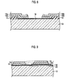
- Fig. 8 shows in schematic section an example of structure of bypass resistor in a first stabilization circuit 120 applied to the semiconductor device 1 according to the first embodiment.
- This structure includes: a substrate 10; a resistor film 18 disposed on the substrate 10; insulation films 12 made up by nitride films or the like and disposed on the substrate 10; metal contact layers 14a and 14b disposed on the insulation films 12, respectively, and configured to contact with the resistor film 18; and metallic layers 16a and 16b connected with the metal contact layers 14a and 14b, respectively.
- the insulation films 12 may be made up by e.g. silicon nitride films, silicon oxide films, silicon oxynitride films, or the like.
- the metal contact layers 14a and 14b may be formed with polysilicon layers, for instance, and the metallic layers 16a and 16b may be made of aluminum (Al), for instance.
- the second stabilization circuit 140 is adapted for cancellation of negative resistance.
- Fig. 10 shows the second stabilization circuit 140 applied to the semiconductor device 1 according to the second embodiment.
- the second stabilization circuit 140 is connected between the drain D1 of the first active element 151 and the drain D2 of the second active element 152, and configured as the parallel circuit of drain bypass resistor Rd 0 , drain bypass capacitor Cd 0 , and drain bypass inductor Ld 0 .
- the second stabilization circuit 140 has the resonant frequency equal to an oscillation frequency of high-frequency negative resistance oscillation. In other words, there is a resonant frequency depending on the parallel circuit of drain bypass resistor Rd 0 , drain bypass capacitor Cd 0 , and drain bypass inductor Ld 0 that equals the oscillation frequency of high-frequency negative resistance oscillation.
- Fig. 11 shows, in a graph, simulation results of a semiconductor device 1 according to the second embodiment.
- the axis of abscissas represents frequencies f in GHz
- the axis of ordinate represents S-parameters in terms of S(1,1) dB and S(2,1) dB.
- the simulation showed an L-C circuit composed of the drain bypass capacitor Cd 0 and the drain bypass inductor Ld 0 , resonating at an odd mode frequency, getting short-circuited over a frequency range from a dc to an input frequency.
- the L-C circuit composed of the drain bypass capacitor Cd 0 and the drain bypass inductor Ld 0 .
- a drain bypass resistor Rd 0 for elimination of a negative resistance at the frequency of Gunn oscillation, to suppress the Gunn oscillation.
- the drain bypass capacitor Cd 0 may be disposed adjacent to the drain bypass inductor Ld 0 , like that in Fig. 4 .
- the drain bypass inductor Ld 0 may be made up by an electrode wiring.
- the second stabilization circuit 140 applied to the semiconductor device 1 has a MIM capacitor structure configured like that shown in Fig. 9 , and redundant description thereof is omitted.
- the second stabilization circuit 140 is adapted for cancellation of negative resistance.
- Fig. 15 shows circuitry of the second amplifier A2 including: combination of a first active element 151 and a second active element 152 connected in parallel with each other between the connection terminal P1 and a pair of connection terminals P2 and P3, and each respectively adapted to work with a negative resistance accompanying a high-frequency negative resistance oscillation; a first stabilization circuit 120 connected between a gate G1 of the first active element 151 and a gate G2 of the second active element 152, and composed as a parallel circuit of a gate bypass resistor Rg 0 , a gate bypass capacitor Cg 0 , and a gate bypass inductor Lg 0 ; and a second stabilization circuit 140 connected between a drain D1 of the first active element 151 and a drain D2 of the second active element 152, and composed as a parallel circuit of a drain bypass resistor Rd 0 , a drain bypass capacitor Cd 0 , and a drain bypass inductor Ld 0 .
- the first stabilization circuit 120 has a
- a second stabilization circuit 140 adapted to have a resonant frequency equal to a frequency of high-frequency negative resistance oscillation. That is, there is a resonant frequency determined in dependence on a parallel circuit of a drain bypass capacitor Cd 0 and a drain bypass inductor Ld 0 , to be equal to the high-frequency negative resistance oscillation frequency.
- the parallel circuit of drain bypass capacitor Cd 0 and drain bypass inductor Ld 0 has a reactance value of infinity depending thereon, thus providing the second stabilization circuit 140 with an equivalent impedance to a drain bypass resistor Rd 0 .
- the drain bypass resistor Rd 0 may thus have an equivalent resistance in absolute value to a negative resistance, allowing for cancellation of the negative resistance by the second stabilization circuit 140.
Abstract
Description
- This application is based upon and claims the benefit of priority from prior Japanese Patent Application No.
P2009-174003 filed on July 27, 2009 - Embodiments described herein relate generally to a semiconductor device.
- There are some types of transistors or amplifiers using Group-III to Group-V compound semiconductors such as a GaAsMESFET (Gallium Arsenide Metal Semiconductor Field Effect Transistor). GaAspHEMT (Gallium Arsenide p channel High Electron Mobility Transistor), andInPHEMT (Indium Phosphide High Electron Mobility Transistor), and susceptive to high-frequency oscillations due to a negative resistance appearing in a drain end output, known as a Gunn oscillation. Such the Gunn oscillation is applicable as an oscillation source of microwaves or millimeter waves, but undesirable for performances of power amplifiers to be stable and highly efficient.
- In such applications using a single FET to operate as an amplifier, there is an accompanied expectation for a stable operation to be free of oscillations over a wide frequency range. However, amplifiers using a single FET have a limitation in output power level. For enhancement of amplifier power level, there are amplifiers using parallel connections of two or more FETs.
- Such parallel connections of amplifiers have individual amplifiers simply bearing part of entire output power, thus affording to increase synthesized output power without undue burdens on individual amplifiers.
- In spite of advantageous possible enhancement of synthesized output power relative to a single FET, parallel-connected FET amplifiers are subject to phenomena of so-called "parallel FET oscillation" or "odd mode oscillation" making them unstable. Such undesirable oscillations are caused by a self-resonant circuit composed of parasitic capacitors in FETs and inductances of wirings for FET connections.
- FETs tend to be broken by odd mode oscillation currents owing to such resonant phenomena.
- For suppression of such undesirable odd mode oscillations, typical parallel FET amplifiers have a resistor connected in series to gates of parallel FETs for reduction of their gate currents. However, serial connection of a resistor to the gate works to reduce also an input signal to be amplified. Hence, there is a desideratum for parallel FET amplifiers to suppress odd mode oscillations without reduction of an input signal to be amplified.
- As an example for suppression of odd mode oscillation in a typical parallel FET amplifier,
Fig. 1 shows use of a bypass resistor Rd0 connected between drains. Further, as an example for suppression of odd mode oscillation in a typical parallel FET amplifier,Fig. 2 shows combination of a gate bypass resistor Rg0 connected between gates, and a drain bypass resistor Rd0 connected between drains. InFig. 1 and Fig. 2 , designated at G1, D1, and S1 are a gate, a drain, and a source of anFET 1, respectively, and G2, D2, and S2 are a gate, a drain, and a source of anFET 2, respectively. InFig. 1 and Fig. 2 , the sources S1 and S2 are grounded. - For parallelization of the
FET 1 and theFET 2 inFig. 1 , the gate G1 ofFET 1 and the gate G2 ofFET 2 are connected to each other, there being inductors Lg accompanying gate wirings between the gate G1 and an input terminal Pi and between the input terminal Pi and the gate G2. - Likewise, for parallelization of the
FET 1 and theFET 2 inFig. 1 , the drain D1 ofFET 1 and the drain D2 ofFET 2 are connected to each other, there being inductors Ld2 accompanying drain wirings between the drain D1 and an output terminal Po and between the output terminal Po and the drain D2. Further, inFig. 1 , there is a bypass resistor Rd0 connected between the drain D1 ofFET 1 and the drain D2 of FET 2 (more specifically, between a node C and a node D), there being inductors Ld1 accompanying associated drain wirings. - For parallelization of the
FET 1 and theFET 2 inFig. 2 , the gate G1 ofFET 1 and the gate G2 ofFET 2 are connected to each other, there being inductors Lg2 accompanying gate wirings between the gate G1 and an input terminal Pi and between the input terminal Pi and the gate G2. Further, inFig. 2 , there is a bypass resistor Rg0 connected between the gate G1 ofFET 1 and the gate G2 of FET 2 (more specifically, between a node A and a node B), there being inductors Lg1 accompanying associated drain wirings. - Likewise, for parallelization of the
FET 1 and theFET 2 inFig. 2 , the drain D1 ofFET 1 and the drain D2 ofFET 2 are connected to each other, there being inductors Ld2 accompanying drain wirings between the drain D1 and an output terminal Po and between the output terminal Po and the drain D2. Further, inFig. 2 , there is a bypass resistor Rd0 connected between the drain D1 ofFET 1 and the drain D2 of FET 2 (more specifically, between a node C and a node D), there being inductors Ld1 accompanying associated drain wirings. - Generally, individual FETs have device variations in between, so there are potential variations developed between gate potentials or drain potentials of individual FETs. It therefore is difficult to cancel out potential variations between gate potentials or drain potentials of individual FETs, even with a bypass resistor connected between gates or drains of parallelized FETs. Further, in use for power amplification, parallelized FETs with such device variations are susceptive in power synthesis ratio to input frequencies accompanying potential variations.
- Further, for parallelization of FETs, there is connection of a parallel circuit composed of a bypass resistor and a bypass inductor between gates and drains, subject to an increase in loss at frequencies of an input to be amplified.
-
-
Fig. 1 is an example of circuitry of a semiconductor device in the past, with a drain bypass resistor Rd0 connected between drains of parallelized FETs. -
Fig. 2 is an example of circuitry of a semiconductor device in the past, with a gate bypass resistor Rg0 connected between gates, and a drain bypass resistor Rd0 connected between drains of parallelized FETs. -
Fig. 3 is a schematic circuit diagram of a semiconductor device according to a first embodiment. -
Fig. 4 is a schematic view of a planar pattern configuration of a stabilization circuit applied to the semiconductor device according to the first embodiment. -
Fig. 5 is a schematic view of a planar pattern configuration of an FET applied to the semiconductor device according to the first embodiment. -
Fig. 6 is a schematic view of a planar pattern configuration of a modified stabilization circuit applied to the semiconductor device according to the first embodiment. -
Fig. 7 is a schematic perspective view of configuration of an interdigital capacitor in a stabilization circuit applied to the semiconductor device according to the first embodiment. -
Fig. 8 is a schematic sectional view of configuration of a resistor in a stabilization circuit applied to the semiconductor device according to the first embodiment. -
Fig. 9 is a schematic sectional view of configuration of a MIM capacitor in a stabilization circuit applied to the semiconductor device according to the first embodiment. -
Fig. 10 is a schematic circuit diagram of a semiconductor device according to a second embodiment. -
Fig. 11 shows simulation results of a semiconductor device according to the second embodiment. -
Fig. 12 is a schematic circuit diagram of a semiconductor device according to a third embodiment. -
Fig. 13 is a schematic circuit block diagram of a semiconductor device according to a modification of the third embodiment. -
Fig. 14 is a schematic circuit diagram of an amplifier A1 at a first stage in the semiconductor device according to the modification of the third embodiment. -
Fig. 15 is a schematic circuit diagram of an amplifier A2 at a second stage in the semiconductor device according to the modification of the third embodiment. -
Fig. 16 is a schematic circuit diagram of an amplifier A3 at a third stage in the semiconductor device according to the modification of the third embodiment. - There will be description of embodiments with reference to the drawings.
- According to an embodiment, there is a semiconductor device comprising a first active element, a second active element connected in parallel with the first active element, and a first stabilization circuit connected between a gate of the first active element and a gate of the second active element, and configured with a parallel circuit of a gate bypass resistor, a gate bypass capacitor, and a gate bypass inductor, wherein the first stabilization circuit has a resonant frequency equal to an odd mode resonant frequency.
- According to another embodiment, there is a semiconductor device comprising a combination of a first active element and a second active element connected in parallel to each other and each respectively adapted to have a negative resistance accompanying a high-frequency negative resistance oscillation, a first stabilization circuit connected between a gate of the first active element and a gate of the second active element, and configured with a parallel circuit of a gate bypass resistor, a gate bypass capacitor, and a gate bypass inductor, and a second stabilization circuit connected between a drain of the first active element and a drain of the second active element, and configured with a parallel circuit of a drain bypass resistor, a drain bypass capacitor, and a drain bypass inductor, wherein the first stabilization circuit has a resonant frequency equal to an odd mode resonant frequency, the second stabilization circuit having a resonant frequency equal to a high-frequency negative resistance oscillation frequency.
- According to another embodiment, there is a semiconductor device comprising a set of active elements connected in parallel to each other and each respectively adapted to work with a negative resistance accompanying a high-frequency negative resistance oscillation, a first stabilization circuit connected between gates of neighboring active elements of the set of active elements and configured with a parallel circuit of a gate bypass resistor, a gate bypass capacitor, and a gate bypass inductor, and a second stabilization circuit connectedbetween drains of the neighboring active elements of the set of active elements, and configured with a parallel circuit of a drain bypass resistor, a drain bypass capacitor, and a drain bypass inductor, wherein the first stabilization circuit has a resonant frequency equal to an odd mode resonant frequency, the second stabilization circuit having a resonant frequency equal to a frequency of high-frequency negative resistance oscillation.
- According to a first embodiment, as schematically shown in
Fig. 3 , there is asemiconductor device 1 configured with circuitry including: combination of a firstactive element 151, and a secondactive element 152 to be connected in parallel with the firstactive element 151; and afirst stabilization circuit 120 connected between a gate G1 of the firstactive element 151 and a gate G2 of the second active element 152 (more specifically, between a node A and a node B), and composed as a parallel circuit of a gate bypass resistor Rg0, a gate bypass capacitor Cg0, and a gate bypass inductor Lg0. Thefirst stabilization circuit 120 has a resonant frequency equal to an odd mode resonance frequency. - The gate bypass capacitor Cg0 may be disposed adjacent to the gate bypass inductor Lg0.
- The gate bypass capacitor Cg0 may be disposed adjacent to the gate bypass resistor Rg0.
- In
Fig. 3 , the firstactive element 151 has the gate, a drain, and a source designated by G1, D1, and S1, respectively, and the secondactive element 152 has the gate, a drain, and a source designated by G2, D2, and S2, respectively. InFig. 3 , the sources S1 and S2 are grounded. - For parallelization of the first
active element 151 and the secondactive element 152, the gate G1 and the gate G2 are connected to each other, as shown inFig. 3 , there being inductors Lg2 accompanying gate wirings between the gate G1 and an input terminal Pi and between the input terminal Pi and the gate G2. Further, thefirst stabilization circuit 120 is connected between the gate G1 and the gate G2, as shown inFig. 3 , there being inductors Lg1 accompanying associated gate wirings. - Likewise, for parallelization of the first
active element 151 and the secondactive element 152, the drain D1 and the drain D2 are connected to each other, as shown inFig. 3 , there being inductors Ld2 accompanying drain wirings between the drain D1 and an output terminal Po and between the output terminal Po and the drain D2. Further, there is a drain bypass resistor Rd0 connected between the drain D1 and the drain D2 (more specifically, between a node C and a node D), as shown inFig. 3 , there being inductors Ld1 accompanying associated drain wirings. - In circuit configuration shown in
Fig. 3 , there are two current-conducting loops to appear in the odd mode oscillation. One is a current-conducting loop at the drain side that conducts a current through the firstactive element 151, from the drain D1 to the source S1, concurrently conducting a current through the secondactive element 152, from the source S2 to the drain D2. Or else, it conducts a current from the source S1 to the drain D1 of the firstactive element 151, concurrently conducting a current from the drain D2 to the source S2 of the secondactive element 152. The other is a current-conducting loop at the gate side that conducts a current through the firstactive element 151, from the gate G1 to the source S1, concurrently conducting a current through the secondactive element 152, from the source S2 to the gate G2. Or else, this conducts a current from the source S1 to the gate G1 of the firstactive element 151, concurrently conducting a current from the gate G2 to the source S2 of the secondactive element 152. - Such odd mode oscillations are produced at the drain side current-conducting loop or the gate side current-conducting loop, by a self-resonant circuit formed with a combination of parasitic capacities in the first
active element 151 and the secondactive element 152 and wiring inductors in circuits for connection of the firstactive element 151 and the secondactive element 152. -
Fig. 3 shows thefirst stabilization circuit 120 applied to thesemiconductor device 1 according to the first embodiment. Thefirst stabilization circuit 120 is connected between the gate G1 of the firstactive element 151 and the gate G2 of the secondactive element 152, and configured as the parallel circuit of gate bypass resistor Rg0, gate bypass capacitor Cg0, and gate bypass inductor Lg0. Thefirst stabilization circuit 120 has the resonant frequency equal to an odd mode resonance frequency. In other words, there is a resonant frequency depending on the parallel circuit of gate bypass resistor Rg0, gate bypass capacitor Cg0, and gate bypass inductor Lg0 that equals the odd mode resonance frequency. - According to the first embodiment, in the state of odd mode oscillation of the
semiconductor device 1, thefirst stabilization circuit 120 has an equivalent impedance to the gate bypass resistor Rg0, because combination of the gate bypass capacitor Cg0 and the gate bypass inductor Lg0 constitutes a parallel circuit that has a reactance of infinity. This can eliminate odd mode oscillations. - The parallel circuit of gate bypass capacitor Cg0 and gate bypass inductor Lg0 gets short-circuited within a range of frequencies from a dc to an input operational frequency, permitting the gate G1 and the gate G2 to have the same electric potential even with piece-to-piece variations between the first
active element 151 and the secondactive element 152. - The first
active element 151 and the secondactive element 152 can thus be set to a gate potential, affording for element variations if any in between to have suppressed effects on the power synthesis ratio, allowing for stable and highly efficient power amplification. - The first
active element 151 and the secondactive element 152 may be configured with an FET, HEMT, Gunn diode, IMPATT diode, or TUNNETT diode. - More specifically, the first
active element 151 and the secondactive element 152 may be configured with a GaAsMESFET, GaAsHEMT, InPHEMT, or such. - According to the first embodiment having the
first stabilization circuit 120 applied to thesemiconductor device 1, there is a semiconductor device provided with a suppressed odd mode oscillation allowing for stable and highly efficient power amplification. -
Fig. 4 schematically shows a planar pattern configuration of astabilization circuit 120 applied to thesemiconductor device 1 according to the first embodiment. Thisstabilization circuit 120 has, between the gate G1 of the firstactive element 151 and the gate G2 of the secondactive element 152 shown inFig. 3 : an R-L circuit composed of a gate bypass resistor Rg0 made up by a thin-film resistor or the like, and a gate bypass inductor Lg0 connected in parallel with the gate bypass resistor Rg0; and a gate bypass capacitor Cg0 formed on the gate bypass resistor Rg0 and connected in parallel with the R-L circuit. - The gate bypass capacitor Cg0 may be disposed adjacent to the gate bypass inductor Lg0, as shown in
Fig. 4 . - The gate bypass capacitor Cg0 may be disposed as a lamination on the gate bypass resistor Rg0, as shown in
Fig. 4 . Or else, the gate bypass capacitor Cg0 may be disposed as a lamination under the gate bypass resistor Rg0. - Or otherwise, the gate bypass capacitor Cg0 may have an interdigital capacitor structure configured with a first
metallic layer 34, and a secondmetallic layer 36 disposed adjacent to the firstmetallic layer 34, as shown inFig. 4 . - The gate bypass inductor Lg0 may be made up by an electrode wiring.
-
Fig. 5 schematically shows an example of planar pattern configuration of anactive element 150 applied to thesemiconductor device 1 according to the first embodiment. Thisactive element 150 includes: asubstrate 10; and combination of asource electrode 20, adrain electrode 22, and agate electrode 24 each respectively disposed on thesubstrate 10, and formed with a set of fingers. Further, it includes: combination of a drain terminal electrode D, a set of gate electrode terminals G1, G2, G3, and G4, and a set of source electrode terminals S1, S2, S3, S4, and S5 each respectively disposed on thesubstrate 10; and a set of via holes SC1, SC2, SC3, SC4, and SC5 for connections to the source electrode terminals S1, S2, S3, S4, and S5, respectively. The drain terminal electrode D is connected with the set of fingers of thedrain electrode 22, the gate electrode terminals G1, G2, G3, and G4, with subsets of the set of fingers of thegate electrode 24, respectively, and the source electrode terminals S1, S2, S3, S4, and S5, with subsets of the set of fingers of thesource electrode 20, respectively. - On the
substrate 10, there is the combination ofsource electrode 20,drain electrode 22, andgate electrode 24 formed with their sets of fingers grouped or sub-grouped as necessary to constitute the terminal electrodes. Thesource electrode 20,drain electrode 22, andgate electrode 24 have the sets of fingers arrayed over an area AA configured to be active, as illustrated inFig. 5 . - The example shown in
Fig. 5 has the gate electrode terminals G1, G2, G3, and G4 and the source electrode terminals S1, S2, S3, S4, and S5 disposed at one side, and the drain terminal electrode D disposed at the opposite side. - The active area AA is formed in a vicinity of surface of the
substrate 10, over an area on thesubstrate 10 under thesource electrode 20,drain electrode 22, andgate electrode 24. - In the example shown in
Fig. 5 , thesubstrate 10 has: the source electrode terminals S1, S2, S3, S4, and S5 formed on corresponding areas on a front side thereof vicinal to the active area AA; the via holes SC1, SC2, SC3, SC4, and SC5 formed through them from corresponding locations on a backside thereof; and a ground conductor formed on the backside. For circuit elements to be grounded, there are electrical connections provided through via holes between the ground conductor at the backside ofsubstrate 10 and circuit elements on the front side ofsubstrate 10. - The
substrate 10 may be: an SiC substrate; a GaAs substrate; a GaN substrate; a substrate with a GaN epitaxial layer formed on an SiC substrate; a substrate with a GaN epitaxial layer formed on an Si substrate; a substrate with a GaN / AlGaN hetero- junction epitaxial layer formed on an SiC substrate; a substrate with a GaN epitaxial layer formed on a sapphire substrate; a sapphire substrate or diamond substrate; or a semi-insulating substrate. - According to the first embodiment, in the
semiconductor device 1, there may beactive elements 150 configured each as shown inFig. 5 , for instance, and applied as the firstactive element 151 and the secondactive element 152 arranged in parallel with each other, in combination with afirst stabilization circuit 120 connected between the gate G1 and the gate G2, as a parallel circuit of a gate bypass resistor Rg0, a gate bypass capacitor Cg0, and a gate bypass inductor Lg0. -
Fig. 6 schematically shows a modified planar pattern configuration ofstabilization circuit 120 applied to thesemiconductor device 1 according to the first embodiment. Thisstabilization circuit 120 has; an R-L circuit composed of a resistor Rg0 made up by a thin-film resistor or the like, and an inductor Lg0 connected in parallel with the resistor Rg0; and a capacitor Cg0 disposed adjacent to the resistor Rg0 and connected in parallel with the R-L circuit. - The capacitor Cg0 may have an interdigital capacitor structure configured with a first
metallic layer 34, and a secondmetallic layer 36 disposed adjacent to the firstmetallic layer 34, as shown inFig. 6 . - The inductor Lg0 may be made up by an electrode wiring.
-
Fig. 7 shows an example of structure of interdigital capacitor in afirst stabilization circuit 120 applied to thesemiconductor device 1 according to the first embodiment. This structure includes: asubstrate 10; an insulatinglayer 32 disposed on thesubstrate 10; a firstmetallic layer 34 disposed on the insulatinglayer 32; and a secondmetallic layer 36 disposed on the insulatinglayer 32, adjacent to the firstmetallic layer 34. The firstmetallic layer 34 as well as the secondmetallic layer 36 may be made of aluminum (Al), for instance, and the insulatinglayer 32 may be made up by e.g. a silicon nitride film, a silicon oxide film, a silicon oxynitride film, or the like. Between the firstmetallic layer 34 and the secondmetallic layer 36, there may be an air gap, or an insulation layer such as SiO2 filled in between. -
Fig. 8 shows in schematic section an example of structure of bypass resistor in afirst stabilization circuit 120 applied to thesemiconductor device 1 according to the first embodiment. This structure includes: asubstrate 10; aresistor film 18 disposed on thesubstrate 10; insulation films 12 made up by nitride films or the like and disposed on thesubstrate 10; metal contact layers 14a and 14b disposed on the insulation films 12, respectively, and configured to contact with theresistor film 18; andmetallic layers metallic layers -
Fig. 9 shows an example of bypass capacitor Cg0 in afirst stabilization circuit 120 applied to thesemiconductor device 1 according to the first embodiment. This bypass capacitor Cg0 has a MIM capacitor structure configured with a thirdmetallic layer 40, aninsulation layer 32 disposed on the thirdmetallic layer 40, and ametal contact layer 14 disposed on theinsulation layer 32. - More specifically,
Fig. 9 shows in schematic section an example of structure of MIM capacitor in afirst stabilization circuit 120 applied to thesemiconductor device 1 according to the first embodiment. This MIM capacitor structure is configured with: asubstrate 10; the thirdmetallic layer 40 disposed on thesubstrate 10; theinsulation layer 32 disposedon thesubstrate 10 and the thirdmetallic layer 40; themetal contact layer 14 disposed on theinsulation layer 32; and ametallic layer 16 disposed on themetal contact layer 14. There is a MIM capacitor structure in the form of thirdmetallic layer 40 /insulation layer 32 /metal contact layer 14 andmetallic layer 16. - According to the first embodiment, there is a semiconductor device provided with a suppressed odd mode oscillation allowing for stable and highly efficient power amplification.
- According to a second embodiment, as schematically shown in
Fig. 10 , there is asemiconductor device 1 configured with circuitry including: combination of a firstactive element 151 and a secondactive element 152 each respectively adapted to work with a negative resistance accompanying a high-frequency negative resistance oscillation; and asecond stabilization circuit 140 connected between a drain D1 of the firstactive element 151 and a drain D2 of the second active element 152 (more specifically, between a node C and a node D), and composed as a parallel circuit of a drain bypass resistor Rd0, a drain bypass capacitor Cd0, and a drain bypass inductor Ld0. Thesecond stabilization circuit 140 has a resonant frequency equal to a high-frequency negative resistance oscillation frequency. - The
second stabilization circuit 140 is adapted for cancellation of negative resistance. - There may be a high-frequency negative resistance oscillation developed as a Gunn oscillation, for instance.
- The drain bypass capacitor Cd0 may be disposed adjacent to the drain bypass inductor Ld0.
- The drain bypass capacitor Cd0 may be disposed adjacent to the drain bypass resistor Rd0.
- In
Fig. 10 , the firstactive element 151 has a gate, the drain, and a source designated by G1, D1, and S1, respectively, and the secondactive element 152 has a gate, the drain, and a source designated by G2, D2, and S2, respectively. InFig. 10 , the sources S1 and S2 are grounded. - For parallelization of the first
active element 151 and the secondactive element 152, the gate G1 and the gate G2 are connected to each other, as shown inFig. 10 , there being inductors Lg accompanying gate wirings between the gate G1 and an input terminal Pi and between the input terminal Pi and the gate G2. - Likewise, for parallelization of the first
active element 151 and the secondactive element 152, the drain D1 and the drain D2 are connected to each other, as shown inFig. 10 , there being inductors Ld2 accompanying drain wirings between the drain D1 and an output terminal Po and between the output terminal Po and the drain D2. Further, thesecond stabilization circuit 140 is connected between the drain D1 and the drain D2, as shown inFig. 10 , there being inductors Ld1 accompanying associated drain wirings. -
Fig. 10 shows thesecond stabilization circuit 140 applied to thesemiconductor device 1 according to the second embodiment. Thesecond stabilization circuit 140 is connected between the drain D1 of the firstactive element 151 and the drain D2 of the secondactive element 152, and configured as the parallel circuit of drain bypass resistor Rd0, drain bypass capacitor Cd0, and drain bypass inductor Ld0. Thesecond stabilization circuit 140 has the resonant frequency equal to an oscillation frequency of high-frequency negative resistance oscillation. In other words, there is a resonant frequency depending on the parallel circuit of drain bypass resistor Rd0, drain bypass capacitor Cd0, and drain bypass inductor Ld0 that equals the oscillation frequency of high-frequency negative resistance oscillation. - According to the second embodiment, in the state of high-frequency negative resistance oscillation of the
semiconductor device 1, thesecond stabilization circuit 140 has an equivalent impedance to the drain bypass resistor Rd0, because combination of the drain bypass capacitor Cd0 and the drain bypass inductor Ld0 constitutes a parallel circuit that has a reactance of infinity. The drain bypass resistor Rd0 can be set to an equivalent resistance to the negative resistance, thus permitting thesecond stabilization circuit 140 to cancel the negative resistance. - There may be a high-frequency negative resistance oscillation developed as a Gunn oscillation, for instance.
-
Fig. 11 shows, in a graph, simulation results of asemiconductor device 1 according to the second embodiment. The axis of abscissas represents frequencies f in GHz, and the axis of ordinate represents S-parameters in terms of S(1,1) dB and S(2,1) dB. There were conditions assumed, including an input frequency of 10 GHz, a Gunn oscillation frequency of 70 GHz, a drain bypass capacitor Cd0 of 0.14 pF, a drain bypass inductor Ld0 of 0.05 nH, and a resonant frequency of 70 GHz for asecond stabilization circuit 140. - The simulation showed an L-C circuit composed of the drain bypass capacitor Cd0 and the drain bypass inductor Ld0, resonating at an odd mode frequency, getting short-circuited over a frequency range from a dc to an input frequency. For the Gunn oscillation frequency sufficiently higher than the input frequency, there was an open state of the L-C circuit composed of the drain bypass capacitor Cd0 and the drain bypass inductor Ld0. As proven, there was successful use of a drain bypass resistor Rd0 for elimination of a negative resistance at the frequency of Gunn oscillation, to suppress the Gunn oscillation.
- The
second stabilization circuit 140 has an LC parallel circuit configured to resonate at a Gunn oscillation frequency, providing an infinite reactance, and is adapted to provide a positive resistance. Hence, in thesemiconductor device 1 according to the second embodiment, there is use of asecond stabilization circuit 140 configured for elimination of a negative resistance at a frequency of Gunn oscillation, to suppress the Gunn oscillation. - There may be a first
active element 151 or a secondactive element 152 configured as an FET, a HEMT, a Gunn diode, an IMPATT diode, or a TUNNETT diode. - More specifically, three may be a first
active element 151 or a secondactive element 152 configured as a GaAsMES FET, a GaAsHEMT, an InPHEMT, or such. - In the
semiconductor device 1 according to the second embodiment, there is use of asecond stabilization circuit 140 configured to suppress a negative resistance accompanying a high-frequency negative resistance oscillation, allowing for provision of a semiconductor device adapted for stable power amplification with an enhanced efficiency. - According to the second embodiment, the
second stabilization circuit 140 applied to thesemiconductor device 1 has a planar pattern configured like that schematically shown inFig. 4 , and redundant description thereof is omitted. - The drain bypass capacitor Cd0 may be disposed adjacent to the drain bypass inductor Ld0, like that in
Fig. 4 . - The drain bypass capacitor Cd0 may be disposed as a lamination on the drain bypass resistor Rd0, like that in
Fig. 4 . Or else, the drain bypass capacitor Cd0 may be disposed as a lamination under the drain bypass resistor Rd0. - Or otherwise, the drain bypass capacitor Cd0 may have an interdigital capacitor structure configured with a first
metallic layer 34, and a secondmetallic layer 36 disposed adjacent to the firstmetallic layer 34, like that inFig. 4 . - The drain bypass inductor Ld0 may be made up by an electrode wiring.
- According to the second embodiment, the
active elements semiconductor device 1 each have a planar pattern configured like that schematically shown inFig. 5 , and redundant description thereof is omitted. - According to the second embodiment, the
second stabilization circuit 140 applied to thesemiconductor device 1 has a modified planar pattern configured like that schematically shown inFig. 6 , and redundant description thereof is omitted. - According to the second embodiment, the
second stabilization circuit 140 applied to thesemiconductor device 1 has an interdigital capacitor structure configured like that shown inFig. 7 , and redundant description thereof is omitted. - According to the second embodiment, the
second stabilization circuit 140 applied to thesemiconductor device 1 has the drain bypass resistor Rd0 configured in section like that schematically shown inFig. 8 , and redundant description thereof is omitted. - According to the second embodiment, the
second stabilization circuit 140 applied to thesemiconductor device 1 has a MIM capacitor structure configured like that shown inFig. 9 , and redundant description thereof is omitted. - According to the second embodiment, there is a semiconductor device provided with a suppressed negative resistance accompanying a Gunn oscillation, allowing for stable power amplification with an enhanced efficiency.
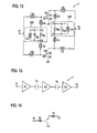
- According to a third embodiment, as schematically shown in
Fig. 12 , there is asemiconductor device 1 configured with circuitry including: combination of a firstactive element 151 and a secondactive element 152 each respectively adapted to work with a negative resistance accompanying a high-frequency negative resistance oscillation; afirst stabilization circuit 120 connected between a gate G1 of the firstactive element 151 and a gate G2 of the second active element 152 (more specifically, between a node A and a node B), and composed as a parallel circuit of a gate bypass resistor Rg0, a gate bypass capacitor Cg0, and a gate bypass inductor Lg0; and asecond stabilization circuit 140 connected between a drain D1 of the firstactive element 151 and a drain D2 of the second active element 152 (more specifically, between a node C and a node D), and composed as a parallel circuit of a drain bypass resistor Rd0, a drain bypass capacitor Cd0, and a drain bypass inductor Ld0. Thefirst stabilization circuit 120 has a resonant frequency equal to an odd mode resonance frequency. Thesecond stabilization circuit 140 has a resonant frequency equal to a high-frequency negative resistance oscillation frequency. - The
second stabilization circuit 140 is adapted for cancellation of negative resistance. - There may be a high-frequency negative resistance oscillation developed as a Gunn oscillation, for instance.
- According to the third embodiment, the
semiconductor device 1 is configured with circuitry including, among others, parasitic inductors accompanying associated wirings, theactive elements second stabilization circuits - The third embodiment may be modified by expanding the configuration of circuitry of semiconductor device shown in
Fig. 12. Fig. 13 shows asemiconductor device 1 according to a modification of the third embodiment. Thissemiconductor device 1 is configured with multi-staged circuitry including: a first amplifier Al connected at an input end thereof to an input terminal Pi of thesemiconductor device 1; a second amplifier A2 coupled at an input end thereof by a first capacitor C1 with an output end of the first amplifier A1; and a third amplifier A3 coupled at an input end thereof by a second capacitor C2 with an output end of the second amplifier A2, and connected at an output end thereof to an output terminal Po of thesemiconductor device 1. -
Fig. 14 shows circuitry of the first amplifier A1 including a single FET provided with a gate inductor lg and a drain inductor ld, and connected between the input terminal Pi and a single connection terminal P1. -
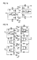
Fig. 15 shows circuitry of the second amplifier A2 including: combination of a firstactive element 151 and a secondactive element 152 connected in parallel with each other between the connection terminal P1 and a pair of connection terminals P2 and P3, and each respectively adapted to work with a negative resistance accompanying a high-frequency negative resistance oscillation; afirst stabilization circuit 120 connected between a gate G1 of the firstactive element 151 and a gate G2 of the secondactive element 152, and composed as a parallel circuit of a gate bypass resistor Rg0, a gate bypass capacitor Cg0, and a gate bypass inductor Lg0; and asecond stabilization circuit 140 connected between a drain D1 of the firstactive element 151 and a drain D2 of the secondactive element 152, and composed as a parallel circuit of a drain bypass resistor Rd0, a drain bypass capacitor Cd0, and a drain bypass inductor Ld0. Thefirst stabilization circuit 120 has a resonant frequency equal to an odd mode resonance frequency. Thesecond stabilization circuit 140 has a resonant frequency equal to a high-frequency negative resistance oscillation frequency. -
Fig. 16 shows circuitry of the third amplifier A3 including: a set of a first pair ofactive elements active elements stabilization circuits 120 each respectively connected between gates G1 and G2, G2 and G3, or G3 and G4 of neighboringactive elements stabilization circuits 140 each respectively connected between drains D1 and D2, D2 and D3, or D3 and D4 of the neighboringactive elements stabilization circuits 120 each have a resonant frequency equal to an odd mode resonance frequency, and thestabilization circuits 140 each have a resonant frequency equal to a high-frequency negative resistance oscillation frequency. - In operation as an amplifier, there is an expectation for a stable performance free of oscillations over a wide frequency range. Instead of an amplifier using a single FET with a limitation in output power, there is a configuration of amplifier using parallel connection of two or more staged FETs for enhancement in power level of amplifier, like the modification of the third embodiment affording for individual FETs to bear simply part of entire output power, allowing for an enhanced synthesis power output without undue burdens on individual FETs.
- According to the modification of the third embodiment, there is possible suppression of both odd mode oscillation and high-frequency negative resistance oscillation in a multi-staged configuration of FET amplifier, allowing for an enhanced synthesis output power, as an advantage relative to a single FET.
- According to the third embodiment, as well as the modification thereof, there is combination of features of a
first stabilization circuit 120 according to the first embodiment and asecond stabilization circuit 140 according to the second embodiment, allowing for suppression of both odd mode oscillation and high-frequency negative resistance oscillation. - That is, there is a resonant frequency determined in dependence on a parallel circuit of a gate bypass capacitor Cg0 and a gate bypass inductor Lg0, to be equal to an odd mode resonant frequency. According to the modification of the third embodiment. in a state of odd mode oscillation of semiconductor device, the parallel circuit of gate bypass capacitor Cg0 and gate bypass inductor Lg0 has a reactance value of infinity depending thereon, thus providing the
first stabilization circuit 120 with an equivalent impedance to a gate bypass resistor Rg0, affording to stop odd mode oscillation. - The parallel circuit of gate bypass capacitor Cg0 and gate bypass inductor Lg0 becomes short-circuited within a frequency range from a dc to input operation frequencies, permitting a set of active elements in use to have an even gate potential, even with device variations among active elements, thus affording to suppress influences of device variations, if any, on the power synthesis ratio, allowing for stable power amplification with an enhanced efficiency.
- Further, there is a
second stabilization circuit 140 adapted to have a resonant frequency equal to a frequency of high-frequency negative resistance oscillation. That is, there is a resonant frequency determined in dependence on a parallel circuit of a drain bypass capacitor Cd0 and a drain bypass inductor Ld0, to be equal to the high-frequency negative resistance oscillation frequency. According to the modification of the third embodiment, in a state of high-frequency negative resistance oscillation of semiconductor device, the parallel circuit of drain bypass capacitor Cd0 and drain bypass inductor Ld0 has a reactance value of infinity depending thereon, thus providing thesecond stabilization circuit 140 with an equivalent impedance to a drain bypass resistor Rd0. The drain bypass resistor Rd0 may thus have an equivalent resistance in absolute value to a negative resistance, allowing for cancellation of the negative resistance by thesecond stabilization circuit 140. - According to the third embodiment, as well as the modification thereof, there is a semiconductor device adapted to suppress an odd mode oscillation, suppressing a negative resistance accompanying the Gunn oscillation, thus allowing for stable power amplification with an enhanced efficiency.
- According to certain embodiments, there may well be a semiconductor device using an amplification element configured not simply as an FET or a HEMT, but also as a LDMOS (Laterally Diffused Metal-Oxide-Semiconductor Field Effect Transistor), or an HBT (Hetero-junction Bipolar Transistor), or a MEMS (Micro Electro Mechanical Systems) or the like.
- While certain embodiments have been described, these embodiments have been presented by way of examples only, and are not intended to limit the scope of the inventions. Indeed, the novel methods and systems described herein may be embodied in a variety of other forms; furthermore, various omissions, substitutions and changes in the form of the methods and systems described herein may be made without departing from the scopes of the inventions. The accompanying claims and their equivalents are intended to cover such forms or modifications as would fall within the scopes of the inventions.
Claims (20)
- A semiconductor device comprising:a first active element;a second active element connected in parallel with the first active element; anda first stabilization circuit connected between a gate of the first active element anda gate of the second active element, and configured with a parallel circuit of a gate bypass resistor, a gate bypass capacitor, and a gate bypass inductor, whereinthe first stabilization circuit has a resonant frequency equal to an odd mode resonant frequency.
- The semiconductor device according to claim 1, wherein
the gate bypass capacitor is disposed adjacent to the gate bypass inductor. - The semiconductor device according to claim 1, wherein the gate bypass capacitor is disposed adjacent to the gate bypass resistor.
- The semiconductor device according to claim 1, wherein the gate bypass capacitor is disposed as a lamination over the gate bypass resistor.
- The semiconductor device according to claim 1, wherein the gate bypass capacitor is disposed as a lamination under the gate bypass resistor.
- The semiconductor device according to claim 1, wherein the gate bypass capacitor has an interdigital capacitor structure comprising a first metallic layer, and a second metallic layer disposed adjacent to the first metallic layer.
- The semiconductor device according to claim 1, wherein the gate bypass capacitor has a MIM capacitor structure comprising a third metallic layer, an insulation layer disposed on the third metallic layer, and a metal contact layer disposed on the insulation layer.
- A semiconductor device comprising:a combination of a first active element and a second active element connected in parallel to each other and each respectively adapted to have a negative resistance accompanying a high-frequency negative resistance oscillation;a first stabilization circuit connected between a gate of the first active element and a gate of the second active element, and configured with a parallel circuit of a gate bypass resistor, a gate bypass capacitor, and a gate bypass inductor, anda second stabilization circuit connected between a drain of the first active element and a drain of the second active element, and configured with a parallel circuit of a drain bypass resistor, a drain bypass capacitor, and a drain bypass inductor,
whereinthe first stabilization circuit has a resonant frequency equal to an odd mode resonant frequency, the second stabilization circuit having a resonant frequency equal to a frequency of high-frequency negative resistance oscillation. - The semiconductor device according to claim 8, wherein the second stabilization circuit is configured to cancel the negative resistance.
- The semiconductor device according to claim 8, wherein the high-frequency negative resistance oscillation is a Gunn oscillation.
- The semiconductor device according to claim 8, wherein the drain bypass capacitor is disposed adjacent to the drain bypass inductor.
- The semiconductor device according to claim 8, wherein the drain bypass capacitor is disposed adjacent to the drain bypass resistor.
- The semiconductor device according to claim 8, wherein the drain bypass capacitor is disposed as a lamination over the drain bypass resistor.
- The semiconductor device according to claim 8, wherein the drain bypass capacitor is disposed as a lamination under the drain bypass resistor.
- The semiconductor device according to claim 8, wherein the drain bypass capacitor has an interdigital capacitor structure comprising a first metallic layer, and a second metallic layer disposed adjacent to the first metallic layer.
- The semiconductor device according to claim 8, wherein the drain bypass capacitor has a MIM capacitor structure comprising a third metallic layer, an insulation layer disposed on the third metallic layer, and a metal contact layer disposed on the insulation layer.
- The semiconductor device according to claim 8, wherein either of the first active element and the second active element comprises a field effect transistor, a high electron mobility transistor, a Gunn diode, an IMPATT diode, or a TUNNETT diode.
- The semiconductor device according to claim 8, wherein either of the first active element and the second active element comprises a field effect transistor comprising:a substrate;a combination of a gate electrode configured with a set of fingers thereof, a source electrode configured with a set of fingers thereof, and a drain electrode configured with a set of fingers thereof, the combination of the gate electrode, the source electrode, and the drain electrode being disposed on the substrate;a combination a gate terminal electrode configured with a subset of the set of fingers of the gate electrode, a source terminal electrode, configured with a subset of the set of fingers of the source electrode, and a drain terminal electrode configured with a subset of the set of fingers of the drain electrode; anda via hole connected to the source terminal electrode.
- A semiconductor device comprising:a set of active elements connected in parallel to each other and each respectively adapted to work with a negative resistance accompanying a high-frequency negative resistance oscillation;a first stabilization circuit connected between gates of neighboring active elements of the set of active elements and configured with a parallel circuit of a gate bypass resistor, a gate bypass capacitor, and a gate bypass inductor, anda second stabilization circuit connected between drains of the neighboring active elements of the set of active elements, and configured with a parallel circuit of a drain bypass resistor, a drain bypass capacitor, and a drain bypass inductor, whereinthe first stabilization circuit has a resonant frequency equal to an odd mode resonant frequency, the second stabilization circuit having a resonant frequency equal to a frequency of high-frequency negative resistance oscillation.
- The semiconductor device according to claim 19, wherein the set of active elements has an active element comprising a field effect transistor or a high electron mobility transistor.
Applications Claiming Priority (1)
| Application Number | Priority Date | Filing Date | Title |
|---|---|---|---|
| JP2009174003A JP5238633B2 (en) | 2009-07-27 | 2009-07-27 | Semiconductor device |
Publications (3)
| Publication Number | Publication Date |
|---|---|
| EP2288020A2 true EP2288020A2 (en) | 2011-02-23 |
| EP2288020A3 EP2288020A3 (en) | 2011-09-07 |
| EP2288020B1 EP2288020B1 (en) | 2012-12-05 |
Family
ID=42990114
Family Applications (1)
| Application Number | Title | Priority Date | Filing Date |
|---|---|---|---|
| EP10250900A Not-in-force EP2288020B1 (en) | 2009-07-27 | 2010-05-10 | Semiconductor device |
Country Status (5)
| Country | Link |
|---|---|
| US (2) | US8022769B2 (en) |
| EP (1) | EP2288020B1 (en) |
| JP (1) | JP5238633B2 (en) |
| KR (1) | KR101104437B1 (en) |
| TW (1) | TWI477066B (en) |
Cited By (1)
| Publication number | Priority date | Publication date | Assignee | Title |
|---|---|---|---|---|
| EP3043470A1 (en) * | 2015-01-09 | 2016-07-13 | Kabushiki Kaisha Toshiba | High frequency signal amplifying circuitry |
Families Citing this family (20)
| Publication number | Priority date | Publication date | Assignee | Title |
|---|---|---|---|---|
| US8324966B2 (en) * | 2011-03-28 | 2012-12-04 | Analog Devices, Inc. | Apparatus and methods for electronic amplification |
| JP5260801B2 (en) * | 2011-05-24 | 2013-08-14 | パナソニック株式会社 | High frequency amplifier circuit |
| JP5487187B2 (en) | 2011-11-16 | 2014-05-07 | 株式会社東芝 | High frequency amplifier |
| JP5711778B2 (en) | 2013-03-06 | 2015-05-07 | 株式会社東芝 | Semiconductor device |
| JP2014175368A (en) * | 2013-03-06 | 2014-09-22 | Toshiba Corp | Field effect transistor and semiconductor device |
| JP6203103B2 (en) | 2014-03-31 | 2017-09-27 | 株式会社東芝 | High frequency semiconductor device |
| EP2988334A3 (en) * | 2014-08-22 | 2016-03-30 | Kabushiki Kaisha Toshiba | Field effect transistor and semiconductor device |
| US9831837B2 (en) * | 2014-11-05 | 2017-11-28 | Qualcomm Incorporated | Dynamic power divider circuits and methods |
| JP6273247B2 (en) * | 2015-12-03 | 2018-01-31 | 株式会社東芝 | High frequency semiconductor amplifier |
| US10128365B2 (en) | 2016-03-17 | 2018-11-13 | Cree, Inc. | Bypassed gate transistors having improved stability |
| JP6658441B2 (en) * | 2016-10-06 | 2020-03-04 | 三菱電機株式会社 | Semiconductor device |
| EP3619738A4 (en) * | 2017-05-05 | 2021-01-13 | Cree, Inc. | High power mmic devices having bypassed gate transistors |
| US10389315B2 (en) * | 2017-06-09 | 2019-08-20 | Qualcomm Incorporated | Three-input continuous-time amplifier and equalizer for multi-level signaling |
| US10483352B1 (en) * | 2018-07-11 | 2019-11-19 | Cree, Inc. | High power transistor with interior-fed gate fingers |
| US10763334B2 (en) | 2018-07-11 | 2020-09-01 | Cree, Inc. | Drain and/or gate interconnect and finger structure |
| US10600746B2 (en) | 2018-07-19 | 2020-03-24 | Cree, Inc. | Radio frequency transistor amplifiers and other multi-cell transistors having gaps and/or isolation structures between groups of unit cell transistors |
| US10938358B2 (en) * | 2018-10-31 | 2021-03-02 | Kabushiki Kaisha Toshiba | Digital power amplifier |
| US10770415B2 (en) | 2018-12-04 | 2020-09-08 | Cree, Inc. | Packaged transistor devices with input-output isolation and methods of forming packaged transistor devices with input-output isolation |
| US11417746B2 (en) | 2019-04-24 | 2022-08-16 | Wolfspeed, Inc. | High power transistor with interior-fed fingers |
| CN116415531A (en) * | 2021-12-29 | 2023-07-11 | 中兴通讯股份有限公司 | InP HEMT small-signal equivalent circuit model, parameter extraction method, equipment and medium |
Family Cites Families (18)
| Publication number | Priority date | Publication date | Assignee | Title |
|---|---|---|---|---|
| JPS6386904A (en) * | 1986-09-30 | 1988-04-18 | Toshiba Corp | Internal matching type high output field effect transistor |
| JPH0281503A (en) * | 1988-09-16 | 1990-03-22 | Mitsubishi Electric Corp | Microwave amplifier circuit |
| JP3120583B2 (en) * | 1992-08-25 | 2000-12-25 | 株式会社デンソー | High frequency amplifier stabilization circuit |
| JP3442208B2 (en) * | 1995-10-26 | 2003-09-02 | 島田理化工業株式会社 | High frequency electronic circuit |
| US5694085A (en) | 1996-02-14 | 1997-12-02 | Glenayre Electronics, Inc. | High-power amplifier using parallel transistors |
| US6005442A (en) * | 1996-03-26 | 1999-12-21 | Matsushita Electric Industrial Co., Ltd. | Divider/combiner |
| JPH11251849A (en) * | 1998-03-04 | 1999-09-17 | Matsushita Electric Ind Co Ltd | High frequency power amplifier |
| KR100260815B1 (en) * | 1998-04-07 | 2000-07-01 | 정선종 | Small signal linearity apparatus |
| US6232840B1 (en) * | 1999-06-10 | 2001-05-15 | Raytheon Company | Transistor amplifier having reduced parasitic oscillations |
| JP2001127544A (en) * | 1999-08-19 | 2001-05-11 | Alps Electric Co Ltd | Two-band oscillator system |
| JP2001274639A (en) * | 2000-03-27 | 2001-10-05 | Toshiba Corp | Semiconductor power amplifier and multi-stage monolithic integrated circuit |
| US6727761B1 (en) * | 2002-09-03 | 2004-04-27 | Triquint Semiconductor, Inc. | Resonant bypassed base ballast circuit |
| JP4756843B2 (en) * | 2004-10-05 | 2011-08-24 | パナソニック株式会社 | Transistor circuit |
| US7348852B1 (en) * | 2004-11-08 | 2008-03-25 | Anadigies, Inc. | Device and method for power amplifier noise reduction |
| JP2007267229A (en) | 2006-03-29 | 2007-10-11 | Toshiba Corp | Microstrip transmission line |
| JP4743077B2 (en) * | 2006-10-23 | 2011-08-10 | 三菱電機株式会社 | High frequency power amplifier |
| JP2009232076A (en) * | 2008-03-21 | 2009-10-08 | Mitsubishi Electric Corp | High-frequency power amplifier |
| JP5185041B2 (en) | 2008-09-25 | 2013-04-17 | 株式会社東芝 | Stabilization circuit and semiconductor device provided with stabilization circuit |
-
2009
- 2009-07-27 JP JP2009174003A patent/JP5238633B2/en not_active Expired - Fee Related
-
2010
- 2010-05-10 EP EP10250900A patent/EP2288020B1/en not_active Not-in-force
- 2010-05-12 KR KR1020100044377A patent/KR101104437B1/en not_active IP Right Cessation
- 2010-05-14 US US12/780,280 patent/US8022769B2/en not_active Expired - Fee Related
- 2010-05-21 TW TW099116293A patent/TWI477066B/en not_active IP Right Cessation
-
2011
- 2011-08-17 US US13/211,806 patent/US8115554B2/en not_active Expired - Fee Related
Non-Patent Citations (1)
| Title |
|---|
| None |
Cited By (2)
| Publication number | Priority date | Publication date | Assignee | Title |
|---|---|---|---|---|
| EP3043470A1 (en) * | 2015-01-09 | 2016-07-13 | Kabushiki Kaisha Toshiba | High frequency signal amplifying circuitry |
| US9748904B2 (en) | 2015-01-09 | 2017-08-29 | Kabushiki Kaisha Toshiba | High frequency signal amplifying circuitry |
Also Published As
| Publication number | Publication date |
|---|---|
| EP2288020B1 (en) | 2012-12-05 |
| US20110298552A1 (en) | 2011-12-08 |
| EP2288020A3 (en) | 2011-09-07 |
| TW201110539A (en) | 2011-03-16 |
| US8022769B2 (en) | 2011-09-20 |
| US8115554B2 (en) | 2012-02-14 |
| JP5238633B2 (en) | 2013-07-17 |
| KR20110011525A (en) | 2011-02-08 |
| KR101104437B1 (en) | 2012-01-12 |
| JP2011029966A (en) | 2011-02-10 |
| US20110018631A1 (en) | 2011-01-27 |
| TWI477066B (en) | 2015-03-11 |
Similar Documents
| Publication | Publication Date | Title |
|---|---|---|
| EP2288020B1 (en) | Semiconductor device | |
| US9543914B2 (en) | Doherty amplifier structure | |
| US8717102B2 (en) | RF device with compensatory resonator matching topology | |
| US8416023B2 (en) | System and method for compensating for changes in an output impedance of a power amplifier | |
| JP5085179B2 (en) | Class F amplifier circuit | |
| US10003311B1 (en) | Compact class-F chip and wire matching topology | |
| US10453810B2 (en) | Integrated passive device for RF power amplifier package | |
| WO2010113779A1 (en) | Semiconductor device | |
| TWI485837B (en) | A high frequency circuit having a multi-chip module structure | |
| US7688152B2 (en) | High frequency stabilization network for microwave devices and monolithic integrated circuits | |
| US10110178B2 (en) | Frequency selective isolation circuit and method for suppressing parametric oscillation | |
| JP6305657B1 (en) | Diode linearizer | |
| JP5185041B2 (en) | Stabilization circuit and semiconductor device provided with stabilization circuit | |
| US20080106353A1 (en) | High-frequency switch | |
| KR100882819B1 (en) | Cascode structure power amplifier using multiple common-gate transistor | |
| US7880549B1 (en) | Transistor including intrinsic harmonic trap | |
| JPH04298105A (en) | Semiconductor amplifier | |
| JP5433768B2 (en) | Semiconductor device provided with stabilization circuit | |
| JP7444251B2 (en) | amplifier circuit | |
| KR101591689B1 (en) | Semiconductor device | |
| JP4311104B2 (en) | Low noise amplifier circuit | |
| JP5328234B2 (en) | Integrated circuit |
Legal Events
| Date | Code | Title | Description |
|---|---|---|---|
| PUAI | Public reference made under article 153(3) epc to a published international application that has entered the european phase |
Free format text: ORIGINAL CODE: 0009012 |
|
| 17P | Request for examination filed |
Effective date: 20100517 |
|
| AK | Designated contracting states |
Kind code of ref document: A2 Designated state(s): AL AT BE BG CH CY CZ DE DK EE ES FI FR GB GR HR HU IE IS IT LI LT LU LV MC MK MT NL NO PL PT RO SE SI SK SM TR |
|
| AX | Request for extension of the european patent |
Extension state: BA ME RS |
|
| PUAL | Search report despatched |
Free format text: ORIGINAL CODE: 0009013 |
|
| AK | Designated contracting states |
Kind code of ref document: A3 Designated state(s): AL AT BE BG CH CY CZ DE DK EE ES FI FR GB GR HR HU IE IS IT LI LT LU LV MC MK MT NL NO PL PT RO SE SI SK SM TR |
|
| AX | Request for extension of the european patent |
Extension state: BA ME RS |
|
| RIC1 | Information provided on ipc code assigned before grant |
Ipc: H03F 3/193 20060101ALI20110803BHEP Ipc: H03F 1/08 20060101AFI20110803BHEP Ipc: H03F 3/21 20060101ALI20110803BHEP Ipc: H03F 1/14 20060101ALI20110803BHEP |
|
| GRAP | Despatch of communication of intention to grant a patent |
Free format text: ORIGINAL CODE: EPIDOSNIGR1 |
|
| GRAS | Grant fee paid |
Free format text: ORIGINAL CODE: EPIDOSNIGR3 |
|
| GRAA | (expected) grant |
Free format text: ORIGINAL CODE: 0009210 |
|
| AK | Designated contracting states |
Kind code of ref document: B1 Designated state(s): AL AT BE BG CH CY CZ DE DK EE ES FI FR GB GR HR HU IE IS IT LI LT LU LV MC MK MT NL NO PL PT RO SE SI SK SM TR |
|
| REG | Reference to a national code |
Ref country code: GB Ref legal event code: FG4D |
|
| REG | Reference to a national code |
Ref country code: CH Ref legal event code: EP |
|
| REG | Reference to a national code |
Ref country code: AT Ref legal event code: REF Ref document number: 587740 Country of ref document: AT Kind code of ref document: T Effective date: 20121215 |
|
| REG | Reference to a national code |
Ref country code: IE Ref legal event code: FG4D |
|
| REG | Reference to a national code |
Ref country code: DE Ref legal event code: R096 Ref document number: 602010003954 Country of ref document: DE Effective date: 20130131 |
|
| REG | Reference to a national code |
Ref country code: AT Ref legal event code: MK05 Ref document number: 587740 Country of ref document: AT Kind code of ref document: T Effective date: 20121205 |
|
| PG25 | Lapsed in a contracting state [announced via postgrant information from national office to epo] |
Ref country code: SE Free format text: LAPSE BECAUSE OF FAILURE TO SUBMIT A TRANSLATION OF THE DESCRIPTION OR TO PAY THE FEE WITHIN THE PRESCRIBED TIME-LIMIT Effective date: 20121205 Ref country code: ES Free format text: LAPSE BECAUSE OF FAILURE TO SUBMIT A TRANSLATION OF THE DESCRIPTION OR TO PAY THE FEE WITHIN THE PRESCRIBED TIME-LIMIT Effective date: 20130316 Ref country code: FI Free format text: LAPSE BECAUSE OF FAILURE TO SUBMIT A TRANSLATION OF THE DESCRIPTION OR TO PAY THE FEE WITHIN THE PRESCRIBED TIME-LIMIT Effective date: 20121205 Ref country code: LT Free format text: LAPSE BECAUSE OF FAILURE TO SUBMIT A TRANSLATION OF THE DESCRIPTION OR TO PAY THE FEE WITHIN THE PRESCRIBED TIME-LIMIT Effective date: 20121205 Ref country code: NO Free format text: LAPSE BECAUSE OF FAILURE TO SUBMIT A TRANSLATION OF THE DESCRIPTION OR TO PAY THE FEE WITHIN THE PRESCRIBED TIME-LIMIT Effective date: 20130305 |
|
| REG | Reference to a national code |
Ref country code: NL Ref legal event code: VDEP Effective date: 20121205 |
|
| REG | Reference to a national code |
Ref country code: LT Ref legal event code: MG4D |
|
| PG25 | Lapsed in a contracting state [announced via postgrant information from national office to epo] |
Ref country code: PL Free format text: LAPSE BECAUSE OF FAILURE TO SUBMIT A TRANSLATION OF THE DESCRIPTION OR TO PAY THE FEE WITHIN THE PRESCRIBED TIME-LIMIT Effective date: 20121205 Ref country code: LV Free format text: LAPSE BECAUSE OF FAILURE TO SUBMIT A TRANSLATION OF THE DESCRIPTION OR TO PAY THE FEE WITHIN THE PRESCRIBED TIME-LIMIT Effective date: 20121205 Ref country code: SI Free format text: LAPSE BECAUSE OF FAILURE TO SUBMIT A TRANSLATION OF THE DESCRIPTION OR TO PAY THE FEE WITHIN THE PRESCRIBED TIME-LIMIT Effective date: 20121205 Ref country code: GR Free format text: LAPSE BECAUSE OF FAILURE TO SUBMIT A TRANSLATION OF THE DESCRIPTION OR TO PAY THE FEE WITHIN THE PRESCRIBED TIME-LIMIT Effective date: 20130306 |
|
| PG25 | Lapsed in a contracting state [announced via postgrant information from national office to epo] |
Ref country code: AT Free format text: LAPSE BECAUSE OF FAILURE TO SUBMIT A TRANSLATION OF THE DESCRIPTION OR TO PAY THE FEE WITHIN THE PRESCRIBED TIME-LIMIT Effective date: 20121205 |
|
| PG25 | Lapsed in a contracting state [announced via postgrant information from national office to epo] |
Ref country code: BG Free format text: LAPSE BECAUSE OF FAILURE TO SUBMIT A TRANSLATION OF THE DESCRIPTION OR TO PAY THE FEE WITHIN THE PRESCRIBED TIME-LIMIT Effective date: 20130305 Ref country code: SK Free format text: LAPSE BECAUSE OF FAILURE TO SUBMIT A TRANSLATION OF THE DESCRIPTION OR TO PAY THE FEE WITHIN THE PRESCRIBED TIME-LIMIT Effective date: 20121205 Ref country code: IS Free format text: LAPSE BECAUSE OF FAILURE TO SUBMIT A TRANSLATION OF THE DESCRIPTION OR TO PAY THE FEE WITHIN THE PRESCRIBED TIME-LIMIT Effective date: 20130405 Ref country code: EE Free format text: LAPSE BECAUSE OF FAILURE TO SUBMIT A TRANSLATION OF THE DESCRIPTION OR TO PAY THE FEE WITHIN THE PRESCRIBED TIME-LIMIT Effective date: 20121205 Ref country code: CZ Free format text: LAPSE BECAUSE OF FAILURE TO SUBMIT A TRANSLATION OF THE DESCRIPTION OR TO PAY THE FEE WITHIN THE PRESCRIBED TIME-LIMIT Effective date: 20121205 Ref country code: BE Free format text: LAPSE BECAUSE OF FAILURE TO SUBMIT A TRANSLATION OF THE DESCRIPTION OR TO PAY THE FEE WITHIN THE PRESCRIBED TIME-LIMIT Effective date: 20121205 |
|
| PG25 | Lapsed in a contracting state [announced via postgrant information from national office to epo] |
Ref country code: NL Free format text: LAPSE BECAUSE OF FAILURE TO SUBMIT A TRANSLATION OF THE DESCRIPTION OR TO PAY THE FEE WITHIN THE PRESCRIBED TIME-LIMIT Effective date: 20121205 Ref country code: PT Free format text: LAPSE BECAUSE OF FAILURE TO SUBMIT A TRANSLATION OF THE DESCRIPTION OR TO PAY THE FEE WITHIN THE PRESCRIBED TIME-LIMIT Effective date: 20130405 Ref country code: RO Free format text: LAPSE BECAUSE OF FAILURE TO SUBMIT A TRANSLATION OF THE DESCRIPTION OR TO PAY THE FEE WITHIN THE PRESCRIBED TIME-LIMIT Effective date: 20121205 |
|
| PLBE | No opposition filed within time limit |
Free format text: ORIGINAL CODE: 0009261 |
|
| STAA | Information on the status of an ep patent application or granted ep patent |
Free format text: STATUS: NO OPPOSITION FILED WITHIN TIME LIMIT |
|
| PG25 | Lapsed in a contracting state [announced via postgrant information from national office to epo] |
Ref country code: DK Free format text: LAPSE BECAUSE OF FAILURE TO SUBMIT A TRANSLATION OF THE DESCRIPTION OR TO PAY THE FEE WITHIN THE PRESCRIBED TIME-LIMIT Effective date: 20121205 |
|
| 26N | No opposition filed |
Effective date: 20130906 |
|
| PG25 | Lapsed in a contracting state [announced via postgrant information from national office to epo] |
Ref country code: CY Free format text: LAPSE BECAUSE OF FAILURE TO SUBMIT A TRANSLATION OF THE DESCRIPTION OR TO PAY THE FEE WITHIN THE PRESCRIBED TIME-LIMIT Effective date: 20121205 |
|
| PG25 | Lapsed in a contracting state [announced via postgrant information from national office to epo] |
Ref country code: IT Free format text: LAPSE BECAUSE OF FAILURE TO SUBMIT A TRANSLATION OF THE DESCRIPTION OR TO PAY THE FEE WITHIN THE PRESCRIBED TIME-LIMIT Effective date: 20121205 Ref country code: MC Free format text: LAPSE BECAUSE OF FAILURE TO SUBMIT A TRANSLATION OF THE DESCRIPTION OR TO PAY THE FEE WITHIN THE PRESCRIBED TIME-LIMIT Effective date: 20121205 |
|
| REG | Reference to a national code |
Ref country code: DE Ref legal event code: R097 Ref document number: 602010003954 Country of ref document: DE Effective date: 20130906 |
|
| PG25 | Lapsed in a contracting state [announced via postgrant information from national office to epo] |
Ref country code: HR Free format text: LAPSE BECAUSE OF FAILURE TO SUBMIT A TRANSLATION OF THE DESCRIPTION OR TO PAY THE FEE WITHIN THE PRESCRIBED TIME-LIMIT Effective date: 20130731 |
|
| REG | Reference to a national code |
Ref country code: IE Ref legal event code: MM4A |
|
| PG25 | Lapsed in a contracting state [announced via postgrant information from national office to epo] |
Ref country code: IE Free format text: LAPSE BECAUSE OF NON-PAYMENT OF DUE FEES Effective date: 20130510 |
|
| REG | Reference to a national code |
Ref country code: CH Ref legal event code: PL |
|
| PG25 | Lapsed in a contracting state [announced via postgrant information from national office to epo] |
Ref country code: LI Free format text: LAPSE BECAUSE OF NON-PAYMENT OF DUE FEES Effective date: 20140531 Ref country code: CH Free format text: LAPSE BECAUSE OF NON-PAYMENT OF DUE FEES Effective date: 20140531 |
|
| PG25 | Lapsed in a contracting state [announced via postgrant information from national office to epo] |
Ref country code: MT Free format text: LAPSE BECAUSE OF FAILURE TO SUBMIT A TRANSLATION OF THE DESCRIPTION OR TO PAY THE FEE WITHIN THE PRESCRIBED TIME-LIMIT Effective date: 20121205 |
|
| PG25 | Lapsed in a contracting state [announced via postgrant information from national office to epo] |
Ref country code: SM Free format text: LAPSE BECAUSE OF FAILURE TO SUBMIT A TRANSLATION OF THE DESCRIPTION OR TO PAY THE FEE WITHIN THE PRESCRIBED TIME-LIMIT Effective date: 20121205 |
|
| PG25 | Lapsed in a contracting state [announced via postgrant information from national office to epo] |
Ref country code: TR Free format text: LAPSE BECAUSE OF FAILURE TO SUBMIT A TRANSLATION OF THE DESCRIPTION OR TO PAY THE FEE WITHIN THE PRESCRIBED TIME-LIMIT Effective date: 20121205 |
|
| PG25 | Lapsed in a contracting state [announced via postgrant information from national office to epo] |
Ref country code: MK Free format text: LAPSE BECAUSE OF FAILURE TO SUBMIT A TRANSLATION OF THE DESCRIPTION OR TO PAY THE FEE WITHIN THE PRESCRIBED TIME-LIMIT Effective date: 20121205 Ref country code: LU Free format text: LAPSE BECAUSE OF NON-PAYMENT OF DUE FEES Effective date: 20130510 Ref country code: HU Free format text: LAPSE BECAUSE OF FAILURE TO SUBMIT A TRANSLATION OF THE DESCRIPTION OR TO PAY THE FEE WITHIN THE PRESCRIBED TIME-LIMIT; INVALID AB INITIO Effective date: 20100510 |
|
| REG | Reference to a national code |
Ref country code: FR Ref legal event code: PLFP Year of fee payment: 7 |
|
| REG | Reference to a national code |
Ref country code: FR Ref legal event code: PLFP Year of fee payment: 8 |
|
| PGFP | Annual fee paid to national office [announced via postgrant information from national office to epo] |
Ref country code: DE Payment date: 20170502 Year of fee payment: 8 |
|
| REG | Reference to a national code |
Ref country code: FR Ref legal event code: PLFP Year of fee payment: 9 |
|
| PGFP | Annual fee paid to national office [announced via postgrant information from national office to epo] |
Ref country code: GB Payment date: 20180329 Year of fee payment: 9 |
|
| PGFP | Annual fee paid to national office [announced via postgrant information from national office to epo] |
Ref country code: FR Payment date: 20180411 Year of fee payment: 9 |
|
| PG25 | Lapsed in a contracting state [announced via postgrant information from national office to epo] |
Ref country code: AL Free format text: LAPSE BECAUSE OF FAILURE TO SUBMIT A TRANSLATION OF THE DESCRIPTION OR TO PAY THE FEE WITHIN THE PRESCRIBED TIME-LIMIT Effective date: 20121205 |
|
| REG | Reference to a national code |
Ref country code: DE Ref legal event code: R119 Ref document number: 602010003954 Country of ref document: DE |
|
| PG25 | Lapsed in a contracting state [announced via postgrant information from national office to epo] |
Ref country code: DE Free format text: LAPSE BECAUSE OF NON-PAYMENT OF DUE FEES Effective date: 20181201 |
|
| GBPC | Gb: european patent ceased through non-payment of renewal fee |
Effective date: 20190510 |
|
| PG25 | Lapsed in a contracting state [announced via postgrant information from national office to epo] |
Ref country code: GB Free format text: LAPSE BECAUSE OF NON-PAYMENT OF DUE FEES Effective date: 20190510 |
|
| PG25 | Lapsed in a contracting state [announced via postgrant information from national office to epo] |
Ref country code: FR Free format text: LAPSE BECAUSE OF NON-PAYMENT OF DUE FEES Effective date: 20190531 |