EP3041047A1 - Metallization for preventing substrate warpage - Google Patents
Metallization for preventing substrate warpage Download PDFInfo
- Publication number
- EP3041047A1 EP3041047A1 EP15202509.4A EP15202509A EP3041047A1 EP 3041047 A1 EP3041047 A1 EP 3041047A1 EP 15202509 A EP15202509 A EP 15202509A EP 3041047 A1 EP3041047 A1 EP 3041047A1
- Authority
- EP
- European Patent Office
- Prior art keywords
- metal layer
- substrate
- additional metal
- warpage
- entire mass
- Prior art date
- Legal status (The legal status is an assumption and is not a legal conclusion. Google has not performed a legal analysis and makes no representation as to the accuracy of the status listed.)
- Granted
Links
Images


Classifications
-
- H—ELECTRICITY
- H05—ELECTRIC TECHNIQUES NOT OTHERWISE PROVIDED FOR
- H05K—PRINTED CIRCUITS; CASINGS OR CONSTRUCTIONAL DETAILS OF ELECTRIC APPARATUS; MANUFACTURE OF ASSEMBLAGES OF ELECTRICAL COMPONENTS
- H05K1/00—Printed circuits
- H05K1/02—Details
-
- H—ELECTRICITY
- H05—ELECTRIC TECHNIQUES NOT OTHERWISE PROVIDED FOR
- H05K—PRINTED CIRCUITS; CASINGS OR CONSTRUCTIONAL DETAILS OF ELECTRIC APPARATUS; MANUFACTURE OF ASSEMBLAGES OF ELECTRICAL COMPONENTS
- H05K1/00—Printed circuits
- H05K1/02—Details
- H05K1/0271—Arrangements for reducing stress or warp in rigid printed circuit boards, e.g. caused by loads, vibrations or differences in thermal expansion
-
- H—ELECTRICITY
- H05—ELECTRIC TECHNIQUES NOT OTHERWISE PROVIDED FOR
- H05K—PRINTED CIRCUITS; CASINGS OR CONSTRUCTIONAL DETAILS OF ELECTRIC APPARATUS; MANUFACTURE OF ASSEMBLAGES OF ELECTRICAL COMPONENTS
- H05K1/00—Printed circuits
- H05K1/02—Details
- H05K1/0201—Thermal arrangements, e.g. for cooling, heating or preventing overheating
-
- H—ELECTRICITY
- H05—ELECTRIC TECHNIQUES NOT OTHERWISE PROVIDED FOR
- H05K—PRINTED CIRCUITS; CASINGS OR CONSTRUCTIONAL DETAILS OF ELECTRIC APPARATUS; MANUFACTURE OF ASSEMBLAGES OF ELECTRICAL COMPONENTS
- H05K1/00—Printed circuits
- H05K1/02—Details
- H05K1/03—Use of materials for the substrate
-
- H—ELECTRICITY
- H05—ELECTRIC TECHNIQUES NOT OTHERWISE PROVIDED FOR
- H05K—PRINTED CIRCUITS; CASINGS OR CONSTRUCTIONAL DETAILS OF ELECTRIC APPARATUS; MANUFACTURE OF ASSEMBLAGES OF ELECTRICAL COMPONENTS
- H05K1/00—Printed circuits
- H05K1/02—Details
- H05K1/03—Use of materials for the substrate
- H05K1/0306—Inorganic insulating substrates, e.g. ceramic, glass
-
- H—ELECTRICITY
- H10—SEMICONDUCTOR DEVICES; ELECTRIC SOLID-STATE DEVICES NOT OTHERWISE PROVIDED FOR
- H10W—GENERIC PACKAGES, INTERCONNECTIONS, CONNECTORS OR OTHER CONSTRUCTIONAL DETAILS OF DEVICES COVERED BY CLASS H10
- H10W70/00—Package substrates; Interposers; Redistribution layers [RDL]
- H10W70/60—Insulating or insulated package substrates; Interposers; Redistribution layers
- H10W70/62—Insulating or insulated package substrates; Interposers; Redistribution layers characterised by their interconnections
- H10W70/65—Shapes or dispositions of interconnections
Definitions
- the present invention relates to a warpage-preventing structure of a substrate, more particularly to a warpage-preventing structure for reducing the warpage of the substrate itself, the warpage which results from the difference in the metal patterns of top and bottom surfaces, and/or the warpage which results from the difference in the thermal expansion coefficients of a metal pattern and the substrate.
- metal-bonded ceramic substrates in which a metal such as copper (Cu) and aluminum (Al) is bonded to a substrate made from ceramic materials such as alumina (Al 2 O 3 ), aluminium nitride (AlN), silicon carbide (SiC) and silicon nitride (Si3N4) have been widely used as components of semiconductor devices.
- a direct bonding copper (DBC) method in which-after a metal plate made from a metal such as copper is placed on a ceramic substrate-the copper plate is directly bonded to the substrate by heating the copper plate at a temperature which is lower than the melting point temperature (1083 °C) of copper and higher than the eutectic point temperature (1065 °C) of copper and oxygen, has been developed and commercially used.
- DBC direct bonding copper
- metal-bonded ceramic substrates have been manufactured by a method of forming the desired circuit patterns by chemically etching a metal plate after the metal plate is bonded to a big ceramic substrate. This method can simultaneously manufacture many circuit substrates, and the manufactured circuit substrate is finally divided into individual substrates by a laser process using carbon dioxide.
- the metal-bonded ceramic substrate manufactured by the above method is usually cut and separated into individual circuit substrates, and then a semiconductor-mounting process is performed.
- a complex arranged substrate manufactured by a laser, not an individual substrate has been developed.
- a complex arranged metal-bonded ceramic substrate is bigger than an individual circuit substrate, it tends to become warped due to its big size. Therefore, in an automation process for mass production, it is difficult to transfer the complex arranged metal-bonded ceramic substrate and fix it in a vacuum environment, and it is liable to be broken when loaded or delivered. Therefore, in order to resolve these problems, various researches for reducing warpage of the complex arranged metal-bonded ceramic substrate have taken place.
- the present invention provides a warpage-preventing structure which can prevent or reduce the warpage of a substrate itself, the warpage resulting from the difference of the metal patterns of the top and bottom surfaces, and/or the warpage resulting from the difference between the thermal expansion coefficient of a metal pattern and that of a ceramic substrate by controlling the entire mass of an additional metal layer which is formed along the edge of the substrate.
- the object of the present invention is not limited to the object mentioned above, and another object which is not mentioned above may be clearly understood by a skilled artisan from the following description.
- the present invention discloses a warpage-preventing structure for preventing warpage of a substrate, wherein at least one metal layer for circuit pattern is disposed on at least one surface of the substrate, the warpage-preventing structure comprising: at least one additional metal layer, wherein the at least one additional metal layer is disposed on at least one surface of the substrate and arranged along an edge of the substrate, wherein at least one additional metal layer pattern is formed on the at least one additional metal layer by removing at least one predetermined area of the at least one additional metal layer.
- the at least one additional metal layer pattern is a plurality of additional metal layer patterns, which are removed to be spaced apart from each other.
- the additional metal layers are formed on a first surface and a second surface of the substrate, and wherein the entire mass of the additional metal layer formed on the first surface of the substrate is different from the entire mass of the additional metal layer formed on the second surface of the substrate.
- the ratio of the entire mass of the additional metal layer formed on the first surface to the entire mass of the additional metal layer formed on the second surface is 1:0.2 to 1:0.8.
- the entire mass of the additional metal layer formed on the first surface is set to be more than the entire mass of the additional metal layer formed on the second surface.
- the entire mass of the additional metal layer formed in the first direction of the substrate is set to be more than the entire mass of the additional metal layer formed in a second direction of the substrate, and wherein the second direction is perpendicular to the first direction.
- the warpage-preventing structure further comprises at least one cutting line which is disposed between the at least one metal layer and the at least one additional metal layer.
- a warpage-preventing structure can prevent or reduce warpage of a metal-bonded substrate by forming an additional metal layer at the outside of a metal layer for circuit pattern which is bonded on at least one surface of a substrate such as a ceramic substrate, and by generating the difference between the entire mass of the additional metal layer formed on the top surface of the substrate and the entire mass of the additional metal layer formed on the bottom surface of the substrate or generating the difference between the entire mass of the additional metal layer disposed perpendicular to a warping direction and the entire mass of the additional metal layer disposed along the warping direction.
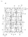
- Fig. 1 is a top view illustrating the top surface of a warpage-preventing structure according to the preferred embodiment of the present invention.
- Fig. 2 is a bottom view illustrating the bottom surface of the warpage-preventing structure according to the preferred embodiment of the present invention.
- Fig. 3 is a sectional view according to line A-A of Figs. 1 and 2 .
- the warpage-preventing structure is a structure for preventing or reducing warpage of a substrate 101, on which a metal layer for circuit pattern 102 is bonded, by arranging an additional metal layer 103.
- the substrate 101 is plate-shaped and made from ceramic materials such as alumina (Al 2 O 3 ), aluminium nitride (AlN), silicon carbide (SiC) and silicon nitride (Si 3 N 4 ), but is not limited thereto.
- the substrate 101 may be warped due to its own weight.
- the metal layer for circuit pattern 102 is bonded to the top surface and/or the bottom surface, and has a shape in which a plurality of circuit pattern areas are repeatedly arranged in horizontal and vertical directions over the entire substrate 101 (hereinafter, the metal layer for circuit pattern 102 is referred to as "metal layer 102," and the substrate 101 on which the metal layer 102 is formed is referred to as "metal-bonded substrate 103"). If the metal layers 102 are formed on the top and bottom surfaces of the substrate 101, the top surface pattern may be different from the bottom surface pattern as illustrated in Figs. 1 and 2 .
- the metal-bonded substrate 103 may be warped due to the shape difference between the pattern of the metal layer 102 bonded to the top surface and the pattern of the metal layer 102 bonded to the bottom surfaces. Furthermore, the metal-bonded substrate 103 may be warped due to the difference between the thermal expansion coefficient of the metal layer 102 and the thermal expansion coefficient of the substrate 101.
- the metal layer 102 may be formed by a direct bonding copper (DBC) method, in which after a metal such as copper is placed on the substrate 101, the copper is directly bonded to the substrate 101 by heating the copper at a temperature which is lower than the melting point temperature (1086°C) of copper and higher than the eutectic point temperature (1065 °C) of copper and oxygen.
- DBC direct bonding copper
- the additional metal layer 110 is added to prevent warpage of the metal-bonded substrate 103.
- the additional metal layer 110 is not used in a semiconductor device but is used so as to increase strength of the metal-bonded substrate 103.
- the additional metal layer 110 is removed after the circuit pattern areas are cut from the metal-bonded substrate 103.
- the additional metal layer 110 is formed along the edges of the top and/or bottom surfaces of the substrate 101 in the shape of a strap.
- the additional metal layers 110 are not included in the circuit patterns.
- the additional metal layer 110 may be continuously formed along the edges of the substrate 101.
- the additional metal layer 110a extended in a width direction and the additional metal layer 110b extended in a length direction, which are formed along the edges of the substrate 101, may be separated and spaced apart from each other.
- the additional metal layer 110 may be made from metals such as copper.
- the additional metal layer 110 is spaced apart from the metal layer 102 and encloses the metal layer 102.
- the additional metal layer pattern 110c is formed on the additional metal layer 110 by removing a predetermined area(s) of the additional metal layer 110.
- the additional metal layer pattern 110c may be formed by a chemical etching method.
- the warpage-preventing substrate according to the present invention can reduce warpage of the metal-bonded substrate 103 by controlling the entire mass of the additional metal layer 110 bonded to one surface of the metal-bonded substrate 103.
- the shape of the additional metal layer pattern 110c may be determined on the basis of the entire mass of the additional metal layer 110 to be removed.
- the additional metal layer pattern 110c may have a plurality of the removed predetermined areas spaced apart from each other and may have a plurality of the additional metal layer areas spaced apart from each other.
- the additional metal layer patterns 110c may be evenly distributed over the entire additional metal layer 110 and may be discontinuously distributed.
- the additional metal layer pattern 110c may have various shapes such as "H,” “I,” “T” and "Y,” and the same shape may be repeatedly arranged or different shapes may be repeatedly arranged.
- the entire mass of the additional metal layer 110 formed on the top surface of the metal-bonded substrate 103 may be set to be different from the entire mass of the additional metal layer 110 formed on the bottom surface of the metal-bonded substrate 103.
- the difference between the entire mass of the additional metal layers 110 formed on the top and bottom surfaces may be between 20% and 80%. That is, preferably the ratio of the entire mass of the additional metal layer 110 formed on one surface of the metal-bonded substrate 103 to the entire mass of the additional metal layer 110 formed on the other surface of the metal-bonded substrate 103 may be between 1:0.2 and 1:0.8.
- the metal-bonded substrate may be fractured. If the difference between the entire mass of the additional metal layers 110 formed on the top and bottom surfaces of the metal-bonded substrate 103 is more than 80%, the warpage degree of the metal-bonded substrate 103 on which the additional metal layers 110 are formed is similar to that of the metal-bonded substrate 103 on which the additional metal layers 110 are not formed. In this case, the process for forming the additional metal layers 110 becomes meaningless.
- the entire mass of the additional metal layer 110 formed on the top surface of the metal-bonded substrate 103 is set to be more than the entire mass of the additional metal layer 110 formed on the bottom surface of the metal-bonded substrate 103. That is, as illustrated in Figs. 1 and 2 , the additional metal layer patterns 110c on the additional metal layer 110 formed on the bottom surface of the metal-bonded substrate 103 are formed to be more than the additional metal layer patterns 110c on the additional metal layer 110 formed on the top surface of the metal-bonded substrate 103.
- the additional metal layer patterns 110c on the additional metal layer 110 formed on the top surface of the metal-bonded substrate 103 should be formed to be more than the additional metal layer patterns 110c on the additional metal layers 110 formed on the bottom surface of the metal-bonded substrate 103. Due to such a difference in the numbers of the additional metal layer patterns 110c, the entire mass of the additional metal layer 110 formed on the bottom surface of the metal-bonded substrate 103 is more than the entire mass of the additional metal layer 110 formed on the top surface of the metal-bonded substrate 103.
- the difference in the entire mass of the additional metal layers 100 may be determined on the basis of the warpage direction. As illustrated in Fig. 4 , if the metal-bonded substrate 103 on which the additional metal layer 110 is not formed is warped along a length direction L, the additional metal layer patterns 110c on the additional metal layer 110a formed along a width direction W are formed to be more than the additional metal layer patterns 110c on the additional metal layer 110b formed along the length direction L. That is, the entire mass of the additional metal layer 110b formed along the length direction L is set to be more than the entire mass of the additional metal layer 110a formed along the width direction W.
- the additional metal layer patterns 110c on the additional metal layer 110b formed along the length direction L are formed to be more than the additional metal layer patterns 110c on the additional metal layer 110a formed along the width direction W. That is, the entire mass of the additional metal layer 110a formed along the width direction W is set to be more than the entire mass of the additional metal layer 110b formed along the length direction L.
- the entire mass of the additional metal layer 110 formed in a direction perpendicular to the warpage-progress direction of the metal-bonded substrate 103 is set to be less than the entire mass of the additional metal layer 110 formed in the warpage-progress direction of the metal-bonded substrate 103. That is, the additional metal layer patterns 103c on the additional metal layer 110 extended in a direction perpendicular to the warpage-progress direction of the metal-bonded substrate 103 are formed to be more than the additional metal layer patterns 103c on the additional metal layer 110 extended in the warpage-progress direction of the metal-bonded substrate 103.
- the warpage-preventing structure 100 may further comprise a cutting line 105.
- the cutting lines 105 are formed between the metal layers 102, and between the metal layer 102 and the additional metal layer 110 to facilitate separating the metal-bonded substrate 103 into individual substrates.
- metal-bonded ceramic substrates were manufactured and experiments for them were performed.
- the metal-bonded ceramic substrates were manufactured in a manner wherein the metal layers for circuit pattern 102 and the additional metal layers 103 were formed on a ceramic substrate as follows.
- the experimental conditions were as follows.
- the metal-bonded ceramic substrate on which the additional metal layer patterns 110c are not formed was warped up to an average of 1757.1 ⁇ m after heat treatment, whereas the warpage of the metal-bonded ceramic substrates (Examples 1-6) according to the present invention was reduced.
- the reducing quantity of warpage was remarkably changed at the ratio of 80%, and the boundary between good and failure (fracture) was formed at the ratio of 20%.
Landscapes
- Engineering & Computer Science (AREA)
- Microelectronics & Electronic Packaging (AREA)
- Chemical & Material Sciences (AREA)
- Ceramic Engineering (AREA)
- Inorganic Chemistry (AREA)
- Manufacturing Of Printed Wiring (AREA)
- Structure Of Printed Boards (AREA)
- Physics & Mathematics (AREA)
- Geometry (AREA)
Abstract
Description
- The present invention relates to a warpage-preventing structure of a substrate, more particularly to a warpage-preventing structure for reducing the warpage of the substrate itself, the warpage which results from the difference in the metal patterns of top and bottom surfaces, and/or the warpage which results from the difference in the thermal expansion coefficients of a metal pattern and the substrate.
- Conventionally, metal-bonded ceramic substrates, in which a metal such as copper (Cu) and aluminum (Al) is bonded to a substrate made from ceramic materials such as alumina (Al2O3), aluminium nitride (AlN), silicon carbide (SiC) and silicon nitride (Si3N4) have been widely used as components of semiconductor devices.
- As a method for bonding a metal plate to a ceramic substrate, a direct bonding copper (DBC) method, in which-after a metal plate made from a metal such as copper is placed on a ceramic substrate-the copper plate is directly bonded to the substrate by heating the copper plate at a temperature which is lower than the melting point temperature (1083 °C) of copper and higher than the eutectic point temperature (1065 °C) of copper and oxygen, has been developed and commercially used. Recently, in order to maintain increase of heat emission and a mechanically strong bonding property, ceramic circuit substrates manufactured by an active metal method, in which metal-bonded circuit substrates are bonded through lead layers, have been developed and used in power semiconductors which demand high reliability.
- Recently, metal-bonded ceramic substrates have been manufactured by a method of forming the desired circuit patterns by chemically etching a metal plate after the metal plate is bonded to a big ceramic substrate. This method can simultaneously manufacture many circuit substrates, and the manufactured circuit substrate is finally divided into individual substrates by a laser process using carbon dioxide.
- The metal-bonded ceramic substrate manufactured by the above method is usually cut and separated into individual circuit substrates, and then a semiconductor-mounting process is performed. In order to increase productivity and work efficiency of the semiconductor-mounting process, a complex arranged substrate manufactured by a laser, not an individual substrate, has been developed. However, since such a complex arranged metal-bonded ceramic substrate is bigger than an individual circuit substrate, it tends to become warped due to its big size. Therefore, in an automation process for mass production, it is difficult to transfer the complex arranged metal-bonded ceramic substrate and fix it in a vacuum environment, and it is liable to be broken when loaded or delivered. Therefore, in order to resolve these problems, various researches for reducing warpage of the complex arranged metal-bonded ceramic substrate have taken place.
-
-
Korean Patent No. 10-1280250 (July 5, 2013 -
Japanese Patent Laid-open Publication No. 2011-216533 (October, 27, 2011 - To resolve the problems of the background arts as explained above, the present invention provides a warpage-preventing structure which can prevent or reduce the warpage of a substrate itself, the warpage resulting from the difference of the metal patterns of the top and bottom surfaces, and/or the warpage resulting from the difference between the thermal expansion coefficient of a metal pattern and that of a ceramic substrate by controlling the entire mass of an additional metal layer which is formed along the edge of the substrate.
- The object of the present invention is not limited to the object mentioned above, and another object which is not mentioned above may be clearly understood by a skilled artisan from the following description.
- The present invention discloses a warpage-preventing structure for preventing warpage of a substrate, wherein at least one metal layer for circuit pattern is disposed on at least one surface of the substrate, the warpage-preventing structure comprising: at least one additional metal layer, wherein the at least one additional metal layer is disposed on at least one surface of the substrate and arranged along an edge of the substrate, wherein at least one additional metal layer pattern is formed on the at least one additional metal layer by removing at least one predetermined area of the at least one additional metal layer.
- The at least one additional metal layer pattern is a plurality of additional metal layer patterns, which are removed to be spaced apart from each other.
- The additional metal layers are formed on a first surface and a second surface of the substrate, and wherein the entire mass of the additional metal layer formed on the first surface of the substrate is different from the entire mass of the additional metal layer formed on the second surface of the substrate.
- The ratio of the entire mass of the additional metal layer formed on the first surface to the entire mass of the additional metal layer formed on the second surface is 1:0.2 to 1:0.8.
- For the substrate which is warped in such a way that the first surface of the substrate is convex, and the second surface of the substrate is concave, the entire mass of the additional metal layer formed on the first surface is set to be more than the entire mass of the additional metal layer formed on the second surface.
- For the substrate which is warped along a first direction, the entire mass of the additional metal layer formed in the first direction of the substrate is set to be more than the entire mass of the additional metal layer formed in a second direction of the substrate, and wherein the second direction is perpendicular to the first direction.
- The warpage-preventing structure further comprises at least one cutting line which is disposed between the at least one metal layer and the at least one additional metal layer.
- A warpage-preventing structure according to the present invention can prevent or reduce warpage of a metal-bonded substrate by forming an additional metal layer at the outside of a metal layer for circuit pattern which is bonded on at least one surface of a substrate such as a ceramic substrate, and by generating the difference between the entire mass of the additional metal layer formed on the top surface of the substrate and the entire mass of the additional metal layer formed on the bottom surface of the substrate or generating the difference between the entire mass of the additional metal layer disposed perpendicular to a warping direction and the entire mass of the additional metal layer disposed along the warping direction.
-
-
Fig. 1 is a top view illustrating the top surface of a warpage-preventing structure according to the preferred embodiment of the present invention. -
Fig. 2 is a bottom view illustrating the bottom surface of the warpage-preventing structure according to the preferred embodiment of the present invention. -
Fig. 3 is a sectional view according to line A-A ofFigs. 1 and2 . -
Fig. 4 is a perspective view of the warpage-preventing structure according to the preferred embodiment of the present invention. - Hereinafter, a warpage-preventing structure according to the preferred embodiment of the present invention will be described in detail with reference to the accompanying drawings. The relevant publicly known functions or structures will not be explained in detail herein if they are not necessary to understand the gist of the present invention.
-
Fig. 1 is a top view illustrating the top surface of a warpage-preventing structure according to the preferred embodiment of the present invention.Fig. 2 is a bottom view illustrating the bottom surface of the warpage-preventing structure according to the preferred embodiment of the present invention.Fig. 3 is a sectional view according to line A-A ofFigs. 1 and2 . - The warpage-preventing structure according to the preferred embodiment of the present invention is a structure for preventing or reducing warpage of a
substrate 101, on which a metal layer forcircuit pattern 102 is bonded, by arranging an additional metal layer 103. - The
substrate 101 is plate-shaped and made from ceramic materials such as alumina (Al2O3), aluminium nitride (AlN), silicon carbide (SiC) and silicon nitride (Si3N4), but is not limited thereto. Thesubstrate 101 may be warped due to its own weight. - The metal layer for
circuit pattern 102 is bonded to the top surface and/or the bottom surface, and has a shape in which a plurality of circuit pattern areas are repeatedly arranged in horizontal and vertical directions over the entire substrate 101 (hereinafter, the metal layer forcircuit pattern 102 is referred to as "metal layer 102," and thesubstrate 101 on which themetal layer 102 is formed is referred to as "metal-bonded substrate 103"). If themetal layers 102 are formed on the top and bottom surfaces of thesubstrate 101, the top surface pattern may be different from the bottom surface pattern as illustrated inFigs. 1 and2 . In this case, the metal-bonded substrate 103 may be warped due to the shape difference between the pattern of themetal layer 102 bonded to the top surface and the pattern of themetal layer 102 bonded to the bottom surfaces. Furthermore, the metal-bonded substrate 103 may be warped due to the difference between the thermal expansion coefficient of themetal layer 102 and the thermal expansion coefficient of thesubstrate 101. - The
metal layer 102 may be formed by a direct bonding copper (DBC) method, in which after a metal such as copper is placed on thesubstrate 101, the copper is directly bonded to thesubstrate 101 by heating the copper at a temperature which is lower than the melting point temperature (1086°C) of copper and higher than the eutectic point temperature (1065 °C) of copper and oxygen. - The
additional metal layer 110 is added to prevent warpage of the metal-bonded substrate 103. Theadditional metal layer 110 is not used in a semiconductor device but is used so as to increase strength of the metal-bonded substrate 103. Theadditional metal layer 110 is removed after the circuit pattern areas are cut from the metal-bonded substrate 103. - The
additional metal layer 110 is formed along the edges of the top and/or bottom surfaces of thesubstrate 101 in the shape of a strap. Theadditional metal layers 110 are not included in the circuit patterns. Theadditional metal layer 110 may be continuously formed along the edges of thesubstrate 101. Furthermore, theadditional metal layer 110a extended in a width direction and theadditional metal layer 110b extended in a length direction, which are formed along the edges of thesubstrate 101, may be separated and spaced apart from each other. - Like the
metal layer 102, theadditional metal layer 110 may be made from metals such as copper. Theadditional metal layer 110 is spaced apart from themetal layer 102 and encloses themetal layer 102. - The additional
metal layer pattern 110c is formed on theadditional metal layer 110 by removing a predetermined area(s) of theadditional metal layer 110. The additionalmetal layer pattern 110c may be formed by a chemical etching method. - Since the additional
metal layer pattern 110c is formed by removing a predetermined area(s) of theadditional metal layer 110, as the additionalmetal layer patterns 110c are further formed, the removed predetermined areas of theadditional metal layer 110 are increased, and thus the entire mass of theadditional metal layer 110 bonded to one surface of thesubstrate 101 is decreased. The warpage-preventing substrate according to the present invention can reduce warpage of the metal-bonded substrate 103 by controlling the entire mass of theadditional metal layer 110 bonded to one surface of the metal-bonded substrate 103. - The shape of the additional
metal layer pattern 110c may be determined on the basis of the entire mass of theadditional metal layer 110 to be removed. The additionalmetal layer pattern 110c may have a plurality of the removed predetermined areas spaced apart from each other and may have a plurality of the additional metal layer areas spaced apart from each other. The additionalmetal layer patterns 110c may be evenly distributed over the entireadditional metal layer 110 and may be discontinuously distributed. The additionalmetal layer pattern 110c may have various shapes such as "H," "I," "T" and "Y," and the same shape may be repeatedly arranged or different shapes may be repeatedly arranged. - If the
additional metal layers 110 are formed on the top and bottom surfaces of the metal-bonded substrate 103, the entire mass of theadditional metal layer 110 formed on the top surface of the metal-bonded substrate 103 may be set to be different from the entire mass of theadditional metal layer 110 formed on the bottom surface of the metal-bonded substrate 103. Preferably, the difference between the entire mass of theadditional metal layers 110 formed on the top and bottom surfaces may be between 20% and 80%. That is, preferably the ratio of the entire mass of theadditional metal layer 110 formed on one surface of the metal-bonded substrate 103 to the entire mass of theadditional metal layer 110 formed on the other surface of the metal-bonded substrate 103 may be between 1:0.2 and 1:0.8. - If the difference between the entire mass of the
additional metal layers 110 formed on the top and bottom surfaces of the metal-bonded substrate 103 is less than 20%, the metal-bonded substrate may be fractured. If the difference between the entire mass of theadditional metal layers 110 formed on the top and bottom surfaces of the metal-bonded substrate 103 is more than 80%, the warpage degree of the metal-bonded substrate 103 on which theadditional metal layers 110 are formed is similar to that of the metal-bonded substrate 103 on which theadditional metal layers 110 are not formed. In this case, the process for forming theadditional metal layers 110 becomes meaningless. - If the
additional metal layers 110 are formed on the top and bottom surfaces of the metal-bonded substrate 103, and the metal-bonded substrate 103 on which theadditional metal layers 110 are not formed is warped to be upwardly convex, the entire mass of theadditional metal layer 110 formed on the top surface of the metal-bonded substrate 103 is set to be more than the entire mass of theadditional metal layer 110 formed on the bottom surface of the metal-bonded substrate 103. That is, as illustrated inFigs. 1 and2 , the additionalmetal layer patterns 110c on theadditional metal layer 110 formed on the bottom surface of the metal-bonded substrate 103 are formed to be more than the additionalmetal layer patterns 110c on theadditional metal layer 110 formed on the top surface of the metal-bonded substrate 103. - Contrary to this, if the metal-bonded substrate 103 on which the
additional metal layer 110 is not formed is warped to be downwardly convex, the additionalmetal layer patterns 110c on theadditional metal layer 110 formed on the top surface of the metal-bonded substrate 103 should be formed to be more than the additionalmetal layer patterns 110c on theadditional metal layers 110 formed on the bottom surface of the metal-bonded substrate 103. Due to such a difference in the numbers of the additionalmetal layer patterns 110c, the entire mass of theadditional metal layer 110 formed on the bottom surface of the metal-bonded substrate 103 is more than the entire mass of theadditional metal layer 110 formed on the top surface of the metal-bonded substrate 103. - The difference in the entire mass of the
additional metal layers 100 may be determined on the basis of the warpage direction. As illustrated inFig. 4 , if the metal-bonded substrate 103 on which theadditional metal layer 110 is not formed is warped along a length direction L, the additionalmetal layer patterns 110c on theadditional metal layer 110a formed along a width direction W are formed to be more than the additionalmetal layer patterns 110c on theadditional metal layer 110b formed along the length direction L. That is, the entire mass of theadditional metal layer 110b formed along the length direction L is set to be more than the entire mass of theadditional metal layer 110a formed along the width direction W. - Contrary to this, if the metal-bonded substrate 103 on which the
additional metal layer 110 is not formed is warped along the width direction W, the additionalmetal layer patterns 110c on theadditional metal layer 110b formed along the length direction L are formed to be more than the additionalmetal layer patterns 110c on theadditional metal layer 110a formed along the width direction W. That is, the entire mass of theadditional metal layer 110a formed along the width direction W is set to be more than the entire mass of theadditional metal layer 110b formed along the length direction L. - In summary, the entire mass of the
additional metal layer 110 formed in a direction perpendicular to the warpage-progress direction of the metal-bonded substrate 103 is set to be less than the entire mass of theadditional metal layer 110 formed in the warpage-progress direction of the metal-bonded substrate 103. That is, the additional metal layer patterns 103c on theadditional metal layer 110 extended in a direction perpendicular to the warpage-progress direction of the metal-bonded substrate 103 are formed to be more than the additional metal layer patterns 103c on theadditional metal layer 110 extended in the warpage-progress direction of the metal-bonded substrate 103. - The warpage-preventing
structure 100 according to an embodiment of the present invention may further comprise acutting line 105. The cutting lines 105 are formed between the metal layers 102, and between themetal layer 102 and theadditional metal layer 110 to facilitate separating the metal-bonded substrate 103 into individual substrates. - In order to confirm the warpage characteristics of the metal-bonded substrate including the warpage-preventing structure according to the present invention, metal-bonded ceramic substrates were manufactured and experiments for them were performed. The metal-bonded ceramic substrates were manufactured in a manner wherein the metal layers for
circuit pattern 102 and the additional metal layers 103 were formed on a ceramic substrate as follows. - Comparative Example: a metal-bonded ceramic substrate on which additional metal layers were not formed.
- Example 1: a metal-bonded ceramic substrate which was manufactured in the same manner as the Comparative Example, except that additional metal layer patterns were formed on the additional metal layer which was on the bottom surface of the substrate and extended in a width direction, and had the entire mass of 86% relative to the entire mass of the additional metal layers on the top surface of the substrate.
- Example 2: a metal-bonded ceramic substrate which was manufactured in the same manner as the Comparative Example, except that additional metal layer patterns were formed on the additional metal layer which was on the bottom surface of the substrate and extended in the width direction, and had the entire mass of 81 % relative to the entire mass of the additional metal layers on the top surface of the substrate.
- Example 3: a metal-bonded ceramic substrate which was manufactured in the same manner as the Comparative Example, except that additional metal layer patterns were formed on the additional metal layer which was on the bottom surface of the substrate and extended in the width direction, and had the entire mass of 63% relative to the entire mass of the additional metal layers on the top surface of the substrate.
- Example 4: a metal-bonded ceramic substrate which was manufactured in the same manner as the Comparative Example, except that additional metal layer patterns were formed on the additional metal layer which was on the bottom surface of the substrate and extended in the width direction, and had the entire mass of 44% relative to the entire mass of the additional metal layers on the top surface of the substrate.
- Example 5: a metal-bonded ceramic substrate which was manufactured in the same manner as the Comparative Example, except that additional metal layer patterns were formed on the additional metal layer which was on the bottom surface of the substrate and extended in the width direction, and had the entire mass of 24% relative to the entire mass of the additional metal layers on the top surface of the substrate.
- Example 6: a metal-bonded ceramic substrate which was manufactured in the same manner as the Comparative Example, except that additional metal layer patterns were formed on the additional metal layer which was on the bottom surface of the substrate and extended in the width direction, and had the entire mass of 0% relative to the entire mass of the additional metal layers on the top surface of the substrate (the additional metal layer, which was on the bottom surface of the substrate and extended in the width direction, was completely removed).
- The experimental conditions were as follows.
- Heat treatment temperature: 270 °C
- Performing one cycle: room temperature for 10 minutes → heated up to 270°C → cooled → room temperature
- Warpage test apparatus: Flatness Measurement and Analysis System, TherMoir Model PS200
- Warpage test method: 10 samples for each Example were manufactured, and warpage values were measured and averaged.
- As shown in Tables 1 and 2, the metal-bonded ceramic substrate on which the additional
metal layer patterns 110c are not formed (Comparative Example) was warped up to an average of 1757.1 µm after heat treatment, whereas the warpage of the metal-bonded ceramic substrates (Examples 1-6) according to the present invention was reduced. In particular, regarding the ratio of the entire mass of the additional metal layers formed on the top surface to the entire mass of the additional metal layers formed on the bottom surface, the reducing quantity of warpage was remarkably changed at the ratio of 80%, and the boundary between good and failure (fracture) was formed at the ratio of 20%. - Although the particular embodiment of the present invention is explained above, it is noted that modifications and variations could be made by a skilled artisan within the scope and spirit of the present invention.
-
- 100:
- Waipage-preventing structure
- 101:
- Substrate
- 102:
- Metal layer for circuit pattern
- 103:
- Metal-bonded substrate
- 110:
- Additional metal layer
- 110a:
- Additional metal layer extended in a width direction
- 110b:
- Additional metal layer extended in a length direction
- 110c:
- Additional metal layer pattern
| Before heat treatment | |||||||
| Comparative example | Example 1 | Example 2 | Example 3 | Example 4 | Example 5 | Example 6 | |
| Entire mass of additional metal layers of top surface | 100% | 100% | 100% | 100% | 100% | 100% | 100% |
| Entire mass of additional metal layers of bottom surface | 100% | 86% | 81% | 63% | 44% | 24% | 0% |
| 1 | 1519 | 1400 | 1294 | 1253 | 1231 | 1188 | 1090 |
| 2 | 1560 | 1344 | 1346 | 1244 | 1280 | 1160 | Fractured |
| 3 | 1513 | 1371 | 1453 | 1410 | 1245 | 1205 | Fractured |
| 4 | 1471 | 1310 | 1207 | 1301 | 1211 | 1250 | 1250 |
| 5 | 1576 | 1014 | 1266 | 1210 | 1270 | 1150 | Fractured |
| 6 | 1372 | 1380 | 1322 | 1200 | 1180 | 1166 | 1160 |
| 7 | 1540 | 1393 | 1257 | 1254 | 1160 | 1260 | 1155 |
| 8 | 1576 | 1258 | 1232 | 1200 | 1210 | 1180 | 1149 |
| 9 | 1208 | 1319 | 1191 | 1311 | 1211 | 1175 | Fractured |
| 10 | 1535 | 1363 | 1427 | 1222 | 1199 | 1210 | 1178 |
| Average | 1487 | 1315.2 | 1299.5 | 1260.5 | 1219.7 | 1194.4 | 1163.667 |
| After heat treatment | |||||||
| Comparative Example | Example 1 | Example 2 | Example 3 | Example 4 | Example 5 | Example 6 | |
| Entire mass of additional metal layers of top surface | 100% | 100% | 100% | 100% | 100% | 100% | 100% |
| Entire mass of additional metal layers of bottom surface | 100% | 86% | 81% | 63% | 44% | 24% | 0% |
| 1 | 1908 | 1071 | 1309 | 1453 | 1431 | 1388 | 1405 |
| 2 | 1807 | 1510 | 1505 | 1444 | 1399 | 1399 | Fractured |
| 3 | 1676 | 1433 | 1405 | 1478 | 1445 | 1405 | Fractured |
| 4 | 1588 | 1503 | 1421 | 1501 | 1411 | 1410 | 1385 |
| 5 | 1868 | 1543 | 1396 | 1350 | 1470 | 1375 | Fractured |
| 6 | 1657 | 1557 | 1293 | 1400 | 1300 | 1366 | 1360 |
| 7 | 1924 | 1549 | 1305 | 1454 | 1310 | 1420 | 1270 |
| 8 | 1815 | 1466 | 1493 | 1310 | 1410 | 1380 | 1380 |
| 9 | 1594 | 1372 | 1476 | 1511 | 1411 | 1250 | Fractured |
| 10 | 1734 | 1577 | 1472 | 1422 | 1299 | 1410 | 1378 |
| Average | 1757.1 | 1458.1 | 1407.5 | 1432.3 | 1388.6 | 1370.3 | 1363 |
Claims (7)
- A warpage-preventing structure for preventing warpage of a substrate, wherein at least one metal layer for circuit pattern is disposed on at least one surface of the substrate, the warpage-preventing structure comprising:At least one additional metal layer, wherein the at least one additional metal layer is disposed on at least one surface of the substrate and arranged along an edge of the substrate,wherein at least one additional metal layer pattern is formed on the at least one additional metal layer by removing at least one predetermined area of the at least one additional metal layer.
- The warpage-preventing structure of Claim 1, wherein
the at least one additional metal layer pattern is a plurality of additional metal layer patterns, which are removed to be spaced apart from each other. - The warpage-preventing structure of Claim 1 or 2, wherein the additional metal layers are formed on a first surface and a second surface of the substrate, and
wherein the entire mass of the additional metal layer formed on the first surface of the substrate is different from the entire mass of the additional metal layer formed on the second surface of the substrate. - The warpage-preventing structure of Claim 3, wherein a ratio of the entire mass of the additional metal layer formed on the first surface to the entire mass of the additional metal layer formed on the second surface is 1:0.2 to 1:0.8.
- The warpage-preventing structure of Claim 3, wherein for the substrate which is warped in such a way that the first surface of the substrate is convex, and the second surface of the substrate is concave, the entire mass of the additional metal layer formed on the first surface is set to be more than the entire mass of the additional metal layer formed on the second surface.
- The warpage-preventing structure of any one of the preceding claims, wherein for the substrate which is warped along a first direction, the entire mass of the additional metal layer formed in the first direction of the substrate is set to be more than the entire mass of the additional metal layer formed in a second direction of the substrate, and wherein the second direction is perpendicular to the first direction.
- The warpage-preventing structure of any one of the preceding claims, further comprising at least one cutting line which is disposed between the at least one metal layer and the at least one additional metal layer.
Applications Claiming Priority (1)
| Application Number | Priority Date | Filing Date | Title |
|---|---|---|---|
| KR1020140192225A KR101733442B1 (en) | 2014-12-29 | 2014-12-29 | Warpage-preventing structure of substrate |
Publications (2)
| Publication Number | Publication Date |
|---|---|
| EP3041047A1 true EP3041047A1 (en) | 2016-07-06 |
| EP3041047B1 EP3041047B1 (en) | 2018-12-19 |
Family
ID=55236135
Family Applications (1)
| Application Number | Title | Priority Date | Filing Date |
|---|---|---|---|
| EP15202509.4A Active EP3041047B1 (en) | 2014-12-29 | 2015-12-23 | Metallization for preventing substrate warpage |
Country Status (3)
| Country | Link |
|---|---|
| US (1) | US9839120B2 (en) |
| EP (1) | EP3041047B1 (en) |
| KR (1) | KR101733442B1 (en) |
Cited By (1)
| Publication number | Priority date | Publication date | Assignee | Title |
|---|---|---|---|---|
| EP3588547A4 (en) * | 2017-02-20 | 2020-08-19 | Shindengen Electric Manufacturing Co. Ltd. | ELECTRONIC DEVICE |
Families Citing this family (2)
| Publication number | Priority date | Publication date | Assignee | Title |
|---|---|---|---|---|
| KR102436225B1 (en) | 2017-07-28 | 2022-08-25 | 삼성전기주식회사 | Printed circuit board |
| CN117886297B (en) * | 2024-01-19 | 2025-02-07 | 兴荣新源(厦门)科技有限公司 | A sodium iron fluorophosphate positive electrode material prepared by repairing and regenerating waste batteries |
Citations (7)
| Publication number | Priority date | Publication date | Assignee | Title |
|---|---|---|---|---|
| EP1345480A2 (en) * | 2002-03-15 | 2003-09-17 | Dowa Mining Co., Ltd. | Ceramic circuit board and power module |
| US20040084205A1 (en) * | 2002-11-05 | 2004-05-06 | Siliconware Precision Industries, Ltd., | Warpage-preventive circuit board and method for fabricating the same |
| US20080012140A1 (en) * | 2006-07-14 | 2008-01-17 | Nec Electronics Corporation | Wiring substrate, semiconductor device, and method of manufacturing the same |
| US20080073784A1 (en) * | 2006-09-27 | 2008-03-27 | Samsung Electronics Co., Ltd. | Circuit substrate for preventing warpage and package using the same |
| US20090133915A1 (en) * | 2004-11-18 | 2009-05-28 | Matsushita Electric Industrial Co., Ltd. | Wiring board, method for manufacturing same and semiconductor device |
| JP2011216533A (en) | 2010-03-31 | 2011-10-27 | Dowa Metaltech Kk | Metal ceramic joined circuit board and method of manufacturing the same |
| KR101280250B1 (en) | 2010-09-30 | 2013-07-05 | 주식회사 케이씨씨 | Metal-bonded ceramic substrate |
Family Cites Families (8)
| Publication number | Priority date | Publication date | Assignee | Title |
|---|---|---|---|---|
| US6534852B1 (en) * | 2000-04-11 | 2003-03-18 | Advanced Semiconductor Engineering, Inc. | Ball grid array semiconductor package with improved strength and electric performance and method for making the same |
| KR20040048429A (en) * | 2001-10-25 | 2004-06-09 | 하리슨 도시바 라이팅 가부시키가이샤 | Light emitting apparatus |
| JP2004200265A (en) * | 2002-12-17 | 2004-07-15 | Nikon Corp | Printed wiring board |
| JP2007019123A (en) * | 2005-07-06 | 2007-01-25 | Sumitomo Metal Electronics Devices Inc | Ceramic circuit board assembly |
| KR101675727B1 (en) * | 2010-03-09 | 2016-11-14 | 주식회사 케이씨씨 | Metal bonded ceramic substrate |
| KR101194456B1 (en) * | 2010-11-05 | 2012-10-24 | 삼성전기주식회사 | Heat-radiating substrate and method for manufacturing the same |
| JP5726037B2 (en) | 2011-09-30 | 2015-05-27 | 三菱電機株式会社 | Semiconductor device |
| US8875390B2 (en) * | 2012-10-29 | 2014-11-04 | Kinsus Interconnect Technology Corp. | Method of manufacturing a laminate circuit board |
-
2014
- 2014-12-29 KR KR1020140192225A patent/KR101733442B1/en active Active
-
2015
- 2015-12-23 EP EP15202509.4A patent/EP3041047B1/en active Active
- 2015-12-29 US US14/982,303 patent/US9839120B2/en not_active Expired - Fee Related
Patent Citations (7)
| Publication number | Priority date | Publication date | Assignee | Title |
|---|---|---|---|---|
| EP1345480A2 (en) * | 2002-03-15 | 2003-09-17 | Dowa Mining Co., Ltd. | Ceramic circuit board and power module |
| US20040084205A1 (en) * | 2002-11-05 | 2004-05-06 | Siliconware Precision Industries, Ltd., | Warpage-preventive circuit board and method for fabricating the same |
| US20090133915A1 (en) * | 2004-11-18 | 2009-05-28 | Matsushita Electric Industrial Co., Ltd. | Wiring board, method for manufacturing same and semiconductor device |
| US20080012140A1 (en) * | 2006-07-14 | 2008-01-17 | Nec Electronics Corporation | Wiring substrate, semiconductor device, and method of manufacturing the same |
| US20080073784A1 (en) * | 2006-09-27 | 2008-03-27 | Samsung Electronics Co., Ltd. | Circuit substrate for preventing warpage and package using the same |
| JP2011216533A (en) | 2010-03-31 | 2011-10-27 | Dowa Metaltech Kk | Metal ceramic joined circuit board and method of manufacturing the same |
| KR101280250B1 (en) | 2010-09-30 | 2013-07-05 | 주식회사 케이씨씨 | Metal-bonded ceramic substrate |
Cited By (1)
| Publication number | Priority date | Publication date | Assignee | Title |
|---|---|---|---|---|
| EP3588547A4 (en) * | 2017-02-20 | 2020-08-19 | Shindengen Electric Manufacturing Co. Ltd. | ELECTRONIC DEVICE |
Also Published As
| Publication number | Publication date |
|---|---|
| KR101733442B1 (en) | 2017-05-10 |
| KR20160080433A (en) | 2016-07-08 |
| US20160192476A1 (en) | 2016-06-30 |
| EP3041047B1 (en) | 2018-12-19 |
| US9839120B2 (en) | 2017-12-05 |
Similar Documents
| Publication | Publication Date | Title |
|---|---|---|
| KR101548091B1 (en) | Method of manufacturing oxide ceramic circuit board, and oxide ceramic circuit board | |
| EP3358615B1 (en) | Silicon nitride circuit board and semiconductor module using same | |
| US9096471B2 (en) | Method for producing a layered material | |
| JP4206915B2 (en) | Power module substrate | |
| KR101675727B1 (en) | Metal bonded ceramic substrate | |
| JPH05129485A (en) | Heat sink dissipating fin and manufacture thereof | |
| EP3780087B1 (en) | Method of manufacturing bonded body for insulating circuit board, and bonded body for insulating circuit board | |
| JP2008235852A (en) | Ceramic substrate and semiconductor module using the same | |
| EP0219254A1 (en) | Joined ceramic-metal composite | |
| JP2018137396A (en) | Manufacturing method of substrate for power module | |
| EP3041047B1 (en) | Metallization for preventing substrate warpage | |
| KR20170048999A (en) | Ceramic Board Manufacturing Method and Ceramic Board manufactured by thereof | |
| EP3761764A1 (en) | Insulating circuit board | |
| JP2017178715A (en) | Manufacturing method of ceramic sintered plate | |
| JP2002057413A (en) | Ceramic substrate and method of manufacturing the same | |
| KR101280250B1 (en) | Metal-bonded ceramic substrate | |
| JP3779074B2 (en) | Ceramic circuit board and power module using it | |
| KR101900547B1 (en) | Loading system for producing ceramic substrate and method of producing ceramic board using thereof | |
| CN101375394A (en) | Package design with reduced warpage | |
| JP7243201B2 (en) | Manufacturing method of insulated circuit board with heat sink and insulated circuit board with heat sink | |
| KR102658985B1 (en) | Bonding head and die bonding apparatus including the same | |
| JP4458999B2 (en) | Multi-circuit board, electronic component storage package and electronic device | |
| KR101953433B1 (en) | apparatus set for producing warpage of ceramic substrate and method for producing warpage of ceramic substrate using there of | |
| JP6422294B2 (en) | Manufacturing method of electronic module substrate and electronic module substrate | |
| WO2020203633A1 (en) | Silicon nitride circuit board, and electronic component module |
Legal Events
| Date | Code | Title | Description |
|---|---|---|---|
| PUAI | Public reference made under article 153(3) epc to a published international application that has entered the european phase |
Free format text: ORIGINAL CODE: 0009012 |
|
| AK | Designated contracting states |
Kind code of ref document: A1 Designated state(s): AL AT BE BG CH CY CZ DE DK EE ES FI FR GB GR HR HU IE IS IT LI LT LU LV MC MK MT NL NO PL PT RO RS SE SI SK SM TR |
|
| AX | Request for extension of the european patent |
Extension state: BA ME |
|
| 17P | Request for examination filed |
Effective date: 20170104 |
|
| RBV | Designated contracting states (corrected) |
Designated state(s): AL AT BE BG CH CY CZ DE DK EE ES FI FR GB GR HR HU IE IS IT LI LT LU LV MC MK MT NL NO PL PT RO RS SE SI SK SM TR |
|
| 17Q | First examination report despatched |
Effective date: 20170327 |
|
| GRAP | Despatch of communication of intention to grant a patent |
Free format text: ORIGINAL CODE: EPIDOSNIGR1 |
|
| INTG | Intention to grant announced |
Effective date: 20180706 |
|
| GRAS | Grant fee paid |
Free format text: ORIGINAL CODE: EPIDOSNIGR3 |
|
| GRAA | (expected) grant |
Free format text: ORIGINAL CODE: 0009210 |
|
| AK | Designated contracting states |
Kind code of ref document: B1 Designated state(s): AL AT BE BG CH CY CZ DE DK EE ES FI FR GB GR HR HU IE IS IT LI LT LU LV MC MK MT NL NO PL PT RO RS SE SI SK SM TR |
|
| REG | Reference to a national code |
Ref country code: GB Ref legal event code: FG4D |
|
| REG | Reference to a national code |
Ref country code: CH Ref legal event code: EP |
|
| REG | Reference to a national code |
Ref country code: IE Ref legal event code: FG4D |
|
| REG | Reference to a national code |
Ref country code: DE Ref legal event code: R096 Ref document number: 602015021798 Country of ref document: DE |
|
| REG | Reference to a national code |
Ref country code: AT Ref legal event code: REF Ref document number: 1079592 Country of ref document: AT Kind code of ref document: T Effective date: 20190115 |
|
| REG | Reference to a national code |
Ref country code: NL Ref legal event code: MP Effective date: 20181219 |
|
| PG25 | Lapsed in a contracting state [announced via postgrant information from national office to epo] |
Ref country code: LV Free format text: LAPSE BECAUSE OF FAILURE TO SUBMIT A TRANSLATION OF THE DESCRIPTION OR TO PAY THE FEE WITHIN THE PRESCRIBED TIME-LIMIT Effective date: 20181219 Ref country code: FI Free format text: LAPSE BECAUSE OF FAILURE TO SUBMIT A TRANSLATION OF THE DESCRIPTION OR TO PAY THE FEE WITHIN THE PRESCRIBED TIME-LIMIT Effective date: 20181219 Ref country code: BG Free format text: LAPSE BECAUSE OF FAILURE TO SUBMIT A TRANSLATION OF THE DESCRIPTION OR TO PAY THE FEE WITHIN THE PRESCRIBED TIME-LIMIT Effective date: 20190319 Ref country code: HR Free format text: LAPSE BECAUSE OF FAILURE TO SUBMIT A TRANSLATION OF THE DESCRIPTION OR TO PAY THE FEE WITHIN THE PRESCRIBED TIME-LIMIT Effective date: 20181219 Ref country code: NO Free format text: LAPSE BECAUSE OF FAILURE TO SUBMIT A TRANSLATION OF THE DESCRIPTION OR TO PAY THE FEE WITHIN THE PRESCRIBED TIME-LIMIT Effective date: 20190319 Ref country code: LT Free format text: LAPSE BECAUSE OF FAILURE TO SUBMIT A TRANSLATION OF THE DESCRIPTION OR TO PAY THE FEE WITHIN THE PRESCRIBED TIME-LIMIT Effective date: 20181219 |
|
| REG | Reference to a national code |
Ref country code: LT Ref legal event code: MG4D |
|
| REG | Reference to a national code |
Ref country code: AT Ref legal event code: MK05 Ref document number: 1079592 Country of ref document: AT Kind code of ref document: T Effective date: 20181219 |
|
| PG25 | Lapsed in a contracting state [announced via postgrant information from national office to epo] |
Ref country code: SE Free format text: LAPSE BECAUSE OF FAILURE TO SUBMIT A TRANSLATION OF THE DESCRIPTION OR TO PAY THE FEE WITHIN THE PRESCRIBED TIME-LIMIT Effective date: 20181219 Ref country code: GR Free format text: LAPSE BECAUSE OF FAILURE TO SUBMIT A TRANSLATION OF THE DESCRIPTION OR TO PAY THE FEE WITHIN THE PRESCRIBED TIME-LIMIT Effective date: 20190320 Ref country code: AL Free format text: LAPSE BECAUSE OF FAILURE TO SUBMIT A TRANSLATION OF THE DESCRIPTION OR TO PAY THE FEE WITHIN THE PRESCRIBED TIME-LIMIT Effective date: 20181219 Ref country code: RS Free format text: LAPSE BECAUSE OF FAILURE TO SUBMIT A TRANSLATION OF THE DESCRIPTION OR TO PAY THE FEE WITHIN THE PRESCRIBED TIME-LIMIT Effective date: 20181219 |
|
| PG25 | Lapsed in a contracting state [announced via postgrant information from national office to epo] |
Ref country code: NL Free format text: LAPSE BECAUSE OF FAILURE TO SUBMIT A TRANSLATION OF THE DESCRIPTION OR TO PAY THE FEE WITHIN THE PRESCRIBED TIME-LIMIT Effective date: 20181219 |
|
| PG25 | Lapsed in a contracting state [announced via postgrant information from national office to epo] |
Ref country code: PT Free format text: LAPSE BECAUSE OF FAILURE TO SUBMIT A TRANSLATION OF THE DESCRIPTION OR TO PAY THE FEE WITHIN THE PRESCRIBED TIME-LIMIT Effective date: 20190419 Ref country code: PL Free format text: LAPSE BECAUSE OF FAILURE TO SUBMIT A TRANSLATION OF THE DESCRIPTION OR TO PAY THE FEE WITHIN THE PRESCRIBED TIME-LIMIT Effective date: 20181219 Ref country code: CZ Free format text: LAPSE BECAUSE OF FAILURE TO SUBMIT A TRANSLATION OF THE DESCRIPTION OR TO PAY THE FEE WITHIN THE PRESCRIBED TIME-LIMIT Effective date: 20181219 Ref country code: ES Free format text: LAPSE BECAUSE OF FAILURE TO SUBMIT A TRANSLATION OF THE DESCRIPTION OR TO PAY THE FEE WITHIN THE PRESCRIBED TIME-LIMIT Effective date: 20181219 Ref country code: IT Free format text: LAPSE BECAUSE OF FAILURE TO SUBMIT A TRANSLATION OF THE DESCRIPTION OR TO PAY THE FEE WITHIN THE PRESCRIBED TIME-LIMIT Effective date: 20181219 |
|
| REG | Reference to a national code |
Ref country code: CH Ref legal event code: PL |
|
| PG25 | Lapsed in a contracting state [announced via postgrant information from national office to epo] |
Ref country code: IS Free format text: LAPSE BECAUSE OF FAILURE TO SUBMIT A TRANSLATION OF THE DESCRIPTION OR TO PAY THE FEE WITHIN THE PRESCRIBED TIME-LIMIT Effective date: 20190419 Ref country code: LU Free format text: LAPSE BECAUSE OF NON-PAYMENT OF DUE FEES Effective date: 20181223 Ref country code: RO Free format text: LAPSE BECAUSE OF FAILURE TO SUBMIT A TRANSLATION OF THE DESCRIPTION OR TO PAY THE FEE WITHIN THE PRESCRIBED TIME-LIMIT Effective date: 20181219 Ref country code: SK Free format text: LAPSE BECAUSE OF FAILURE TO SUBMIT A TRANSLATION OF THE DESCRIPTION OR TO PAY THE FEE WITHIN THE PRESCRIBED TIME-LIMIT Effective date: 20181219 Ref country code: EE Free format text: LAPSE BECAUSE OF FAILURE TO SUBMIT A TRANSLATION OF THE DESCRIPTION OR TO PAY THE FEE WITHIN THE PRESCRIBED TIME-LIMIT Effective date: 20181219 Ref country code: SM Free format text: LAPSE BECAUSE OF FAILURE TO SUBMIT A TRANSLATION OF THE DESCRIPTION OR TO PAY THE FEE WITHIN THE PRESCRIBED TIME-LIMIT Effective date: 20181219 |
|
| REG | Reference to a national code |
Ref country code: IE Ref legal event code: MM4A |
|
| REG | Reference to a national code |
Ref country code: DE Ref legal event code: R097 Ref document number: 602015021798 Country of ref document: DE |
|
| REG | Reference to a national code |
Ref country code: BE Ref legal event code: MM Effective date: 20181231 |
|
| PLBE | No opposition filed within time limit |
Free format text: ORIGINAL CODE: 0009261 |
|
| STAA | Information on the status of an ep patent application or granted ep patent |
Free format text: STATUS: NO OPPOSITION FILED WITHIN TIME LIMIT |
|
| PG25 | Lapsed in a contracting state [announced via postgrant information from national office to epo] |
Ref country code: IE Free format text: LAPSE BECAUSE OF NON-PAYMENT OF DUE FEES Effective date: 20181223 Ref country code: MC Free format text: LAPSE BECAUSE OF FAILURE TO SUBMIT A TRANSLATION OF THE DESCRIPTION OR TO PAY THE FEE WITHIN THE PRESCRIBED TIME-LIMIT Effective date: 20181219 Ref country code: AT Free format text: LAPSE BECAUSE OF FAILURE TO SUBMIT A TRANSLATION OF THE DESCRIPTION OR TO PAY THE FEE WITHIN THE PRESCRIBED TIME-LIMIT Effective date: 20181219 Ref country code: DK Free format text: LAPSE BECAUSE OF FAILURE TO SUBMIT A TRANSLATION OF THE DESCRIPTION OR TO PAY THE FEE WITHIN THE PRESCRIBED TIME-LIMIT Effective date: 20181219 |
|
| 26N | No opposition filed |
Effective date: 20190920 |
|
| PG25 | Lapsed in a contracting state [announced via postgrant information from national office to epo] |
Ref country code: BE Free format text: LAPSE BECAUSE OF NON-PAYMENT OF DUE FEES Effective date: 20181231 |
|
| PG25 | Lapsed in a contracting state [announced via postgrant information from national office to epo] |
Ref country code: CH Free format text: LAPSE BECAUSE OF NON-PAYMENT OF DUE FEES Effective date: 20181231 Ref country code: LI Free format text: LAPSE BECAUSE OF NON-PAYMENT OF DUE FEES Effective date: 20181231 |
|
| PG25 | Lapsed in a contracting state [announced via postgrant information from national office to epo] |
Ref country code: MT Free format text: LAPSE BECAUSE OF NON-PAYMENT OF DUE FEES Effective date: 20181223 |
|
| PG25 | Lapsed in a contracting state [announced via postgrant information from national office to epo] |
Ref country code: SI Free format text: LAPSE BECAUSE OF FAILURE TO SUBMIT A TRANSLATION OF THE DESCRIPTION OR TO PAY THE FEE WITHIN THE PRESCRIBED TIME-LIMIT Effective date: 20181219 Ref country code: FR Free format text: LAPSE BECAUSE OF NON-PAYMENT OF DUE FEES Effective date: 20190219 |
|
| PG25 | Lapsed in a contracting state [announced via postgrant information from national office to epo] |
Ref country code: TR Free format text: LAPSE BECAUSE OF FAILURE TO SUBMIT A TRANSLATION OF THE DESCRIPTION OR TO PAY THE FEE WITHIN THE PRESCRIBED TIME-LIMIT Effective date: 20181219 |
|
| PG25 | Lapsed in a contracting state [announced via postgrant information from national office to epo] |
Ref country code: MK Free format text: LAPSE BECAUSE OF NON-PAYMENT OF DUE FEES Effective date: 20181219 Ref country code: CY Free format text: LAPSE BECAUSE OF FAILURE TO SUBMIT A TRANSLATION OF THE DESCRIPTION OR TO PAY THE FEE WITHIN THE PRESCRIBED TIME-LIMIT Effective date: 20181219 |
|
| GBPC | Gb: european patent ceased through non-payment of renewal fee |
Effective date: 20191223 |
|
| PG25 | Lapsed in a contracting state [announced via postgrant information from national office to epo] |
Ref country code: GB Free format text: LAPSE BECAUSE OF NON-PAYMENT OF DUE FEES Effective date: 20191223 |
|
| REG | Reference to a national code |
Ref country code: DE Ref legal event code: R079 Ref document number: 602015021798 Country of ref document: DE Free format text: PREVIOUS MAIN CLASS: H01L0023498000 Ipc: H10W0070620000 |
|
| PGFP | Annual fee paid to national office [announced via postgrant information from national office to epo] |
Ref country code: DE Payment date: 20251208 Year of fee payment: 11 |
|
| PGFP | Annual fee paid to national office [announced via postgrant information from national office to epo] |
Ref country code: HU Payment date: 20260129 Year of fee payment: 11 |