EP3040982A1 - Gate drive circuit, gate driving method, and display device - Google Patents
Gate drive circuit, gate driving method, and display device Download PDFInfo
- Publication number
- EP3040982A1 EP3040982A1 EP15777855.6A EP15777855A EP3040982A1 EP 3040982 A1 EP3040982 A1 EP 3040982A1 EP 15777855 A EP15777855 A EP 15777855A EP 3040982 A1 EP3040982 A1 EP 3040982A1
- Authority
- EP
- European Patent Office
- Prior art keywords
- gate
- duration
- voltage
- driving control
- order
- Prior art date
- Legal status (The legal status is an assumption and is not a legal conclusion. Google has not performed a legal analysis and makes no representation as to the accuracy of the status listed.)
- Ceased
Links
Images

Classifications
-
- G—PHYSICS
- G09—EDUCATION; CRYPTOGRAPHY; DISPLAY; ADVERTISING; SEALS
- G09G—ARRANGEMENTS OR CIRCUITS FOR CONTROL OF INDICATING DEVICES USING STATIC MEANS TO PRESENT VARIABLE INFORMATION
- G09G3/00—Control arrangements or circuits, of interest only in connection with visual indicators other than cathode-ray tubes
- G09G3/20—Control arrangements or circuits, of interest only in connection with visual indicators other than cathode-ray tubes for presentation of an assembly of a number of characters, e.g. a page, by composing the assembly by combination of individual elements arranged in a matrix no fixed position being assigned to or needed to be assigned to the individual characters or partial characters
- G09G3/2092—Details of a display terminals using a flat panel, the details relating to the control arrangement of the display terminal and to the interfaces thereto
- G09G3/2096—Details of the interface to the display terminal specific for a flat panel
-
- G—PHYSICS
- G09—EDUCATION; CRYPTOGRAPHY; DISPLAY; ADVERTISING; SEALS
- G09G—ARRANGEMENTS OR CIRCUITS FOR CONTROL OF INDICATING DEVICES USING STATIC MEANS TO PRESENT VARIABLE INFORMATION
- G09G3/00—Control arrangements or circuits, of interest only in connection with visual indicators other than cathode-ray tubes
- G09G3/20—Control arrangements or circuits, of interest only in connection with visual indicators other than cathode-ray tubes for presentation of an assembly of a number of characters, e.g. a page, by composing the assembly by combination of individual elements arranged in a matrix no fixed position being assigned to or needed to be assigned to the individual characters or partial characters
- G09G3/2007—Display of intermediate tones
-
- G—PHYSICS
- G09—EDUCATION; CRYPTOGRAPHY; DISPLAY; ADVERTISING; SEALS
- G09G—ARRANGEMENTS OR CIRCUITS FOR CONTROL OF INDICATING DEVICES USING STATIC MEANS TO PRESENT VARIABLE INFORMATION
- G09G3/00—Control arrangements or circuits, of interest only in connection with visual indicators other than cathode-ray tubes
- G09G3/20—Control arrangements or circuits, of interest only in connection with visual indicators other than cathode-ray tubes for presentation of an assembly of a number of characters, e.g. a page, by composing the assembly by combination of individual elements arranged in a matrix no fixed position being assigned to or needed to be assigned to the individual characters or partial characters
- G09G3/2007—Display of intermediate tones
- G09G3/2018—Display of intermediate tones by time modulation using two or more time intervals
-
- G—PHYSICS
- G09—EDUCATION; CRYPTOGRAPHY; DISPLAY; ADVERTISING; SEALS
- G09G—ARRANGEMENTS OR CIRCUITS FOR CONTROL OF INDICATING DEVICES USING STATIC MEANS TO PRESENT VARIABLE INFORMATION
- G09G5/00—Control arrangements or circuits for visual indicators common to cathode-ray tube indicators and other visual indicators
- G09G5/18—Timing circuits for raster scan displays
-
- G—PHYSICS
- G09—EDUCATION; CRYPTOGRAPHY; DISPLAY; ADVERTISING; SEALS
- G09G—ARRANGEMENTS OR CIRCUITS FOR CONTROL OF INDICATING DEVICES USING STATIC MEANS TO PRESENT VARIABLE INFORMATION
- G09G2310/00—Command of the display device
- G09G2310/02—Addressing, scanning or driving the display screen or processing steps related thereto
- G09G2310/0264—Details of driving circuits
- G09G2310/0267—Details of drivers for scan electrodes, other than drivers for liquid crystal, plasma or OLED displays
-
- G—PHYSICS
- G09—EDUCATION; CRYPTOGRAPHY; DISPLAY; ADVERTISING; SEALS
- G09G—ARRANGEMENTS OR CIRCUITS FOR CONTROL OF INDICATING DEVICES USING STATIC MEANS TO PRESENT VARIABLE INFORMATION
- G09G2310/00—Command of the display device
- G09G2310/08—Details of timing specific for flat panels, other than clock recovery
-
- G—PHYSICS
- G09—EDUCATION; CRYPTOGRAPHY; DISPLAY; ADVERTISING; SEALS
- G09G—ARRANGEMENTS OR CIRCUITS FOR CONTROL OF INDICATING DEVICES USING STATIC MEANS TO PRESENT VARIABLE INFORMATION
- G09G2320/00—Control of display operating conditions
- G09G2320/02—Improving the quality of display appearance
- G09G2320/0247—Flicker reduction other than flicker reduction circuits used for single beam cathode-ray tubes
-
- G—PHYSICS
- G09—EDUCATION; CRYPTOGRAPHY; DISPLAY; ADVERTISING; SEALS
- G09G—ARRANGEMENTS OR CIRCUITS FOR CONTROL OF INDICATING DEVICES USING STATIC MEANS TO PRESENT VARIABLE INFORMATION
- G09G2320/00—Control of display operating conditions
- G09G2320/02—Improving the quality of display appearance
- G09G2320/0257—Reduction of after-image effects
-
- G—PHYSICS
- G09—EDUCATION; CRYPTOGRAPHY; DISPLAY; ADVERTISING; SEALS
- G09G—ARRANGEMENTS OR CIRCUITS FOR CONTROL OF INDICATING DEVICES USING STATIC MEANS TO PRESENT VARIABLE INFORMATION
- G09G3/00—Control arrangements or circuits, of interest only in connection with visual indicators other than cathode-ray tubes
- G09G3/20—Control arrangements or circuits, of interest only in connection with visual indicators other than cathode-ray tubes for presentation of an assembly of a number of characters, e.g. a page, by composing the assembly by combination of individual elements arranged in a matrix no fixed position being assigned to or needed to be assigned to the individual characters or partial characters
- G09G3/34—Control arrangements or circuits, of interest only in connection with visual indicators other than cathode-ray tubes for presentation of an assembly of a number of characters, e.g. a page, by composing the assembly by combination of individual elements arranged in a matrix no fixed position being assigned to or needed to be assigned to the individual characters or partial characters by control of light from an independent source
- G09G3/36—Control arrangements or circuits, of interest only in connection with visual indicators other than cathode-ray tubes for presentation of an assembly of a number of characters, e.g. a page, by composing the assembly by combination of individual elements arranged in a matrix no fixed position being assigned to or needed to be assigned to the individual characters or partial characters by control of light from an independent source using liquid crystals
- G09G3/3611—Control of matrices with row and column drivers
- G09G3/3674—Details of drivers for scan electrodes
- G09G3/3677—Details of drivers for scan electrodes suitable for active matrices only
Definitions
- the present disclosure relates to the field of display technology, and more particularly, to a gate driving circuit, a gate driving method, and a display apparatus.
- An amorphous silicon bottom gate type Thin Film Transistor (TFT), as a switch element, is primarily characterized in that there is a jump voltage ( ⁇ Vp) at a switching instant, and when different voltages are applied to the TFT, the generated jump voltages ⁇ Vp are also different. In a flicker pattern, such jump voltage may results in a problem that an image flickers seriously.
- ⁇ Vp jump voltage
- a low order voltage (the low order voltage and a high order voltage commonly form a multi-order gate voltage MLG) is generally provided before gate off to reduce ⁇ Vp, thereby improving the flicker phenomenon.
- the longer the low order voltage is applied the more obvious the effect of overcoming the flicker phenomenon is.
- the charging time for each pixel in one frame is relatively short.
- the low order voltage is applied for a long time, the charging rate for the pixel is not sufficient, which will influence the display quality.
- the low order voltage is applied for a short time, the effect of overcoming the flicker phenomenon is not sufficiently obvious, i.e., the flicker phenomenon due to ⁇ Vp cannot be effectively avoided.
- embodiments of the present disclosure provide a gate driving circuit and a gate driving method which can not only avoid image flicker but also can avoid V-Block.
- a gate driving circuit comprising: a driving control unit and a gate signal generation unit, wherein the driving control unit is configured to generate different driving control signals suitable for different display patterns; and the gate signal generation unit is connected to the driving control unit and is configured to generate a multi-order gate voltage in response to the driving control signal generated by the driving control unit, wherein duration of a low order voltage included in the generated multi-order gate voltage corresponds to the respective display pattern.
- the driving control unit comprises: a timing controller and multiple controlled switch unit, wherein the timing controller has multiple pulse signal output ends suitable for generating multiple pulse signals and is configured to output pulse signals with different widths through different pulse signal output ends, wherein a pulse signal is suitable for a display pattern; and each of the controlled switch units is arranged between a pulse signal output end of the timing controller and a driving control signal input end of the gate signal generation unit, and various controlled switch units are connected to different pulse signal output ends,
- the multi-order gate voltage is generated by the gate signal generation unit in response to the pulse signal, and comprises a low order voltage in duration consistent with a width of the pulse signal.
- the various controlled switch units are transistors having first electrodes respectively connected to pulse signal output ends of the timing controller and second electrodes respectively connected to driving control signal input ends of the gate signal generation unit.
- the driving control unit further comprises a controller connected to a control end of each controlled switch unit, and configured to control turn-on/turn-off of the respective controlled switch unit in response to the detected display pattern.
- the timing controller is suitable for generating three pulse signals with different widths suitable for a normal pattern, a flicker pattern, and a gray level mode respectively.
- a gate driving method comprising:
- a driving control signal corresponding to a current display pattern according to the current display pattern; and generating, by a gate signal generation unit, a multi-order gate voltage according to the driving control signal, wherein duration of a low order voltage included in the generated multi-order gate voltage corresponds to the respective display pattern.
- the gate signal generation unit in a flicker pattern, the gate signal generation unit generates a multi-order gate voltage having a low order voltage in first duration; in a normal display pattern, the gate signal generation unit generates a multi-order gate voltage having a low order voltage in second duration; and in a gray level mode, the gate signal generation unit generates a multi-order gate voltage having a low order voltage in third duration, wherein the first duration is larger than the second duration and the second duration is larger than the third duration.
- a display apparatus comprising the gate driving circuit described in any of the above embodiments.
- the gate driving circuit comprises a driving control unit 10 configured to generate a driving control signal corresponding to a respective display pattern; and a gate signal generation unit 20 connected to the driving control unit 10 and configured to generate a multi-order gate voltage in response to the driving control signal generated by the driving control unit 10, wherein duration of a low order voltage included in the generated multi-order gate voltage corresponds to the respective display pattern.
- the driving control unit can generate a corresponding driving control signal in a respective display pattern
- the driving signal generation unit can determine a current display pattern according to a current input driving control signal, and generate a multi-order gate voltage having a low order voltage in duration corresponding to the respective display pattern.
- duration of a low order voltage in a particular display pattern may be set according to the requirements of those skilled in the art.
- the terms "corresponding" means that the low order gate voltage in the respective multi-order gate voltage can avoid the display problem generated in the display pattern.
- low order voltage in the embodiments of the present disclosure refer to a voltage with a smaller absolute value in the multi-order gate voltage. Specifically, for an active-high gate voltage, the low order voltage should be lower than the high level voltage, and for an active-low gate voltage, an absolute value of the low order voltage should be lower than an absolute value of the low level signal.
- the gate driving circuit according to the present disclosure can achieve driving for display by using a multi-order gate voltage having a low order voltage in long duration when the display pattern of the display apparatus is a flicker pattern, so as to eliminate the undesirable phenomenon that an image flickers, and achieve driving for display by using a multi-order gate voltage having a low order voltage in short duration when the display pattern is a gray level mode, so as to avoid V-Block, thereby improving the quality of the image display. Even if the whole effective gate voltage signal has short duration, the gate driving circuit according to the embodiments of the present disclosure can also prevent the V-Block phenomenon while avoiding the image from flickering. The effect of avoiding the image from flickering is more obvious especially in a high PPI display apparatus.
- the gate signal generation unit here may be a conventional driver Integrated Circuit (Driver-IC).
- Driver-IC driver Integrated Circuit
- the following description is given by taking the gate signal generation unit being a Driver-IC as an example.
- the Driver-IC is used to generate a gate voltage signal required for driving a gate. In practical applications, various effective gate voltage signals for driving and controlling have the same duration.
- the driving control unit 20 in Fig. 1 may specifically comprise:
- the TCON has at least three pulse signal output ends OE1, OE2 and OE3, which can generate three pulse signals with different widths, and output the pulse signals through respective pulse signal output ends, wherein the three pulse signals with different widths correspond to a display pattern, a flicker pattern, and a gray level mode respectively.
- a first end of the first controlled switch unit T1 is connected to OE1, a first end of the second controlled switch unit is connected to OE2, and a first end of the third switch unit is connected to OE3.
- Second ends of various controlled switch units are connected to driving control signal input ends of the Driver-IC.
- the low order voltage has the longest duration in the flicker pattern, has smaller duration in the normal pattern than the flicker pattern, and has the smallest duration in the gray level mode.
- the pulse signals become the driving control signal.
- the Driver-IC generates respective multi-order gate voltages in response to the pulse signals with different duration.
- the Driver-IC may generate a multi-order gate voltage in response to a pulse signal, wherein the multi-order gate voltage comprises a low order voltage in duration consistent with a width of the pulse signal.
- a particular controlled switch unit may be controlled to turn on at the right time by applying suitable control signals to the control ends of various controlled switch units, so that the Driver-IC generates a suitable multi-order gate voltage, thereby improving the image quality.
- the TCON further comprises a clock signal output end for outputting a clock signal STV to achieve image synchronization.
- Fig. 2 illustrates a condition that the TCON generates three pulse signals with different widths and outputs the pulse signals through three pulse signal output ends
- the TCON may also only generate two pulse signals with different widths and output the pulse signals through two pulse signal output ends, which can also avoid the problems of flicker and V-Block at the same time.
- the same problem can also be solved by generating more than three pulse signals with different widths and providing more than three output ends.
- Such scheme may have a relatively complex design.
- Such configuration in the embodiments of the present disclosure has an advantage of providing a multi-order gate voltage corresponding to a normal display pattern, to achieve a better display effect and a relatively simple design.
- the driving control unit illustrated in Fig. 2 has features of a simple structure and ease of control. However, in practical applications, the functions of the driving control unit may also be achieved by other structures. That is, the structure in Fig. 2 should not be construed as limiting the protection scope of the present disclosure.
- various controlled units T1, T2 and T3 are transistors.
- T1, T2 and T3 have first electrodes respectively connected to the pulse signal output ends OE1-OE3 of the TCON, and second electrodes respectively connected to the driving control signal input ends of the Driver IC.
- switch units which can be turned on or turned off according to the control signal may also be selected.
- the width of the pulse signal finally determines the duration of the low order voltage in the multi-order gate voltage.
- OE1 when T1 is turned on, OE1 inputs a pulse signal with a width of t1 to the Driver-IC. In this case, the duration of the low order voltage in the multi-order gate voltage MLG1 generated by the Driver-IC is also t1.
- T2 when T2 is turned on, OE2 inputs a pulse signal with a width of t2 to the Driver-IC. In this case, the duration of the low order voltage in the multi-order gate voltage MLG2 generated by the Driver-IC is also t2.
- OE3 When T3 is turned on, OE3 inputs a pulse signal with a width of t3 to the Driver-IC.
- the duration of the low order voltage in the multi-order gate voltage MLG3 generated by the Driver-IC is also t3. Further, it can be seen from the figure that the total duration of various effective multi-order gate voltages MLG1, MLG2 and MLG3 should be consistent, and have the same starting position as that of the STV.
- the driving control unit further comprises a controller MCU, which is connected to control ends (gates) of various controlled switch units and controls turn-on/turn-off of respective controlled switch units according to the detected display type.
- a controller MCU which is connected to control ends (gates) of various controlled switch units and controls turn-on/turn-off of respective controlled switch units according to the detected display type.
- the controller here may be a main controller MCU of the whole display apparatus, which controls the light-emitting and display of the whole display apparatus, and can acquire the display pattern of the next frame before the next frame is displayed.
- the main controller controls turn-on/turn-off of various switch units according to the display pattern of the next frame.
- the embodiments of the present disclosure further provide a gate driving method, comprising:
- a driving control signal corresponding to a current display pattern according to the current display pattern
- a gate signal generation unit generating, by a gate signal generation unit, a multi-order gate voltage according to the driving control signal, wherein duration of a low order voltage included in the generated multi-order gate voltage corresponds to the respective display pattern.
- a multi-order gate voltage having a low order voltage in long duration is applied, which can better prohibit a jump voltage of the switch TFT and reduce the flicker degree.
- a multi-order gate voltage having a low order voltage in short duration is applied, which can better improve the charging rate and avoid the phenomenon of V-Block.
- the duration of the low order voltage in the applied multi-order gate voltage is between the long duration and the short duration described above, which achieves moderate charging time for a capacitor, and is beneficial for improving the image quality.
- the multi-order voltage is a two-order voltage
- the low order voltage may have a value equal to 30%-60% of a normal driving voltage, and have duration which occupies 5%-50% of the duration of the whole multi-order voltage.
- the gate driving method according to the embodiments of the present disclosure may be achieved by the above gate driving circuit.
- the embodiments of the present disclosure further provide a display apparatus, comprising the gate driving circuit described in any of the above embodiments.
- the display apparatus here may be any product or component having a display function such as an electronic paper, a mobile phone, a tablet computer, a television, a display, a notebook computer, a digital photo frame, a navigator or the like.
Landscapes
- Engineering & Computer Science (AREA)
- Physics & Mathematics (AREA)
- Computer Hardware Design (AREA)
- General Physics & Mathematics (AREA)
- Theoretical Computer Science (AREA)
- Multimedia (AREA)
- Control Of Indicators Other Than Cathode Ray Tubes (AREA)
- Liquid Crystal Display Device Control (AREA)
- Control Of El Displays (AREA)
Abstract
Description
- The present disclosure relates to the field of display technology, and more particularly, to a gate driving circuit, a gate driving method, and a display apparatus.
- An amorphous silicon bottom gate type Thin Film Transistor (TFT), as a switch element, is primarily characterized in that there is a jump voltage (Δ Vp) at a switching instant, and when different voltages are applied to the TFT, the generated jump voltages Δ Vp are also different. In a flicker pattern, such jump voltage may results in a problem that an image flickers seriously.
- In view of the above problem, a low order voltage (the low order voltage and a high order voltage commonly form a multi-order gate voltage MLG) is generally provided before gate off to reduce Δ Vp, thereby improving the flicker phenomenon. The longer the low order voltage is applied, the more obvious the effect of overcoming the flicker phenomenon is. However, in a high resolution display apparatus, the charging time for each pixel in one frame is relatively short. As a result, if the low order voltage is applied for a long time, the charging rate for the pixel is not sufficient, which will influence the display quality. If the low order voltage is applied for a short time, the effect of overcoming the flicker phenomenon is not sufficiently obvious, i.e., the flicker phenomenon due to Δ Vp cannot be effectively avoided.
- Therefore, embodiments of the present disclosure provide a gate driving circuit and a gate driving method which can not only avoid image flicker but also can avoid V-Block.
- According to an aspect of the present disclosure, a gate driving circuit is provided, comprising: a driving control unit and a gate signal generation unit, wherein the driving control unit is configured to generate different driving control signals suitable for different display patterns; and the gate signal generation unit is connected to the driving control unit and is configured to generate a multi-order gate voltage in response to the driving control signal generated by the driving control unit, wherein duration of a low order voltage included in the generated multi-order gate voltage corresponds to the respective display pattern.
- In an implementation of the present disclosure, the driving control unit comprises: a timing controller and multiple controlled switch unit, wherein the timing controller has multiple pulse signal output ends suitable for generating multiple pulse signals and is configured to output pulse signals with different widths through different pulse signal output ends, wherein a pulse signal is suitable for a display pattern; and each of the controlled switch units is arranged between a pulse signal output end of the timing controller and a driving control signal input end of the gate signal generation unit, and various controlled switch units are connected to different pulse signal output ends,
- wherein the multi-order gate voltage is generated by the gate signal generation unit in response to the pulse signal, and comprises a low order voltage in duration consistent with a width of the pulse signal.
- In an implementation of the present disclosure, the various controlled switch units are transistors having first electrodes respectively connected to pulse signal output ends of the timing controller and second electrodes respectively connected to driving control signal input ends of the gate signal generation unit.
- In an implementation of the present disclosure, the driving control unit further comprises a controller connected to a control end of each controlled switch unit, and configured to control turn-on/turn-off of the respective controlled switch unit in response to the detected display pattern.
- In an implementation of the present disclosure, the timing controller is suitable for generating three pulse signals with different widths suitable for a normal pattern, a flicker pattern, and a gray level mode respectively.
- According to another aspect of the present disclosure, a gate driving method is provided, comprising:
- generating a driving control signal corresponding to a current display pattern according to the current display pattern; and generating, by a gate signal generation unit, a multi-order gate voltage according to the driving control signal, wherein duration of a low order voltage included in the generated multi-order gate voltage corresponds to the respective display pattern.
- In an implementation of the present disclosure, in a flicker pattern, the gate signal generation unit generates a multi-order gate voltage having a low order voltage in first duration; in a normal display pattern, the gate signal generation unit generates a multi-order gate voltage having a low order voltage in second duration; and in a gray level mode, the gate signal generation unit generates a multi-order gate voltage having a low order voltage in third duration, wherein the first duration is larger than the second duration and the second duration is larger than the third duration.
- According to another aspect of the present disclosure, a display apparatus is provided, comprising the gate driving circuit described in any of the above embodiments.
-
-
Fig. 1 illustrates a structural diagram of a gate driving circuit according to an embodiment of the present disclosure; -
Fig. 2 illustrates a structural diagram of a driving control unit inFig. 1 ; and -
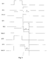
Fig. 3 illustrates a timing diagram of a part of signals in a gate driving circuit according to an embodiment of the present application. - Detailed description of the present disclosure will be further described below in conjunction with accompanying drawings and embodiments. The following embodiments are merely used to illustrate the technical solutions of the present disclosure more clearly, instead of limiting the protection scope of the present disclosure.
- The embodiments of the present disclosure provide a gate driving circuit. As shown in
Fig. 1 , the gate driving circuit comprises adriving control unit 10 configured to generate a driving control signal corresponding to a respective display pattern; and a gatesignal generation unit 20 connected to thedriving control unit 10 and configured to generate a multi-order gate voltage in response to the driving control signal generated by thedriving control unit 10, wherein duration of a low order voltage included in the generated multi-order gate voltage corresponds to the respective display pattern. - Those skilled in the art should understand that in the embodiments of the present disclosure, as the driving control unit can generate a corresponding driving control signal in a respective display pattern, the driving signal generation unit can determine a current display pattern according to a current input driving control signal, and generate a multi-order gate voltage having a low order voltage in duration corresponding to the respective display pattern. In a specific implementation, duration of a low order voltage in a particular display pattern may be set according to the requirements of those skilled in the art. In order to achieve a better display effect, the terms "corresponding" means that the low order gate voltage in the respective multi-order gate voltage can avoid the display problem generated in the display pattern.
- It should be understood that the terms "low order voltage" in the embodiments of the present disclosure refer to a voltage with a smaller absolute value in the multi-order gate voltage. Specifically, for an active-high gate voltage, the low order voltage should be lower than the high level voltage, and for an active-low gate voltage, an absolute value of the low order voltage should be lower than an absolute value of the low level signal.
- The gate driving circuit according to the present disclosure can achieve driving for display by using a multi-order gate voltage having a low order voltage in long duration when the display pattern of the display apparatus is a flicker pattern, so as to eliminate the undesirable phenomenon that an image flickers, and achieve driving for display by using a multi-order gate voltage having a low order voltage in short duration when the display pattern is a gray level mode, so as to avoid V-Block, thereby improving the quality of the image display. Even if the whole effective gate voltage signal has short duration, the gate driving circuit according to the embodiments of the present disclosure can also prevent the V-Block phenomenon while avoiding the image from flickering. The effect of avoiding the image from flickering is more obvious especially in a high PPI display apparatus.
- Specifically, the gate signal generation unit here may be a conventional driver Integrated Circuit (Driver-IC). The following description is given by taking the gate signal generation unit being a Driver-IC as an example. The Driver-IC is used to generate a gate voltage signal required for driving a gate. In practical applications, various effective gate voltage signals for driving and controlling have the same duration.
- In an alternative implementation, as shown in
Fig. 2 , thedriving control unit 20 inFig. 1 may specifically comprise: - a timing controller TCON and three controlled switch units T1, T2 and T3. The TCON has at least three pulse signal output ends OE1, OE2 and OE3, which can generate three pulse signals with different widths, and output the pulse signals through respective pulse signal output ends, wherein the three pulse signals with different widths correspond to a display pattern, a flicker pattern, and a gray level mode respectively. A first end of the first controlled switch unit T1 is connected to OE1, a first end of the second controlled switch unit is connected to OE2, and a first end of the third switch unit is connected to OE3. Second ends of various controlled switch units are connected to driving control signal input ends of the Driver-IC. Generally, the low order voltage has the longest duration in the flicker pattern, has smaller duration in the normal pattern than the flicker pattern, and has the smallest duration in the gray level mode.
- In this case, the pulse signals become the driving control signal. The Driver-IC generates respective multi-order gate voltages in response to the pulse signals with different duration.
- More specifically, the Driver-IC may generate a multi-order gate voltage in response to a pulse signal, wherein the multi-order gate voltage comprises a low order voltage in duration consistent with a width of the pulse signal.
- In practical applications, a particular controlled switch unit may be controlled to turn on at the right time by applying suitable control signals to the control ends of various controlled switch units, so that the Driver-IC generates a suitable multi-order gate voltage, thereby improving the image quality.
- In a specific implementation, as shown in
Fig. 2 , the TCON further comprises a clock signal output end for outputting a clock signal STV to achieve image synchronization. - It should be noted that although
Fig. 2 illustrates a condition that the TCON generates three pulse signals with different widths and outputs the pulse signals through three pulse signal output ends, in practical applications, the TCON may also only generate two pulse signals with different widths and output the pulse signals through two pulse signal output ends, which can also avoid the problems of flicker and V-Block at the same time. The same problem can also be solved by generating more than three pulse signals with different widths and providing more than three output ends. However, such scheme may have a relatively complex design. Such configuration in the embodiments of the present disclosure has an advantage of providing a multi-order gate voltage corresponding to a normal display pattern, to achieve a better display effect and a relatively simple design. - The driving control unit illustrated in
Fig. 2 has features of a simple structure and ease of control. However, in practical applications, the functions of the driving control unit may also be achieved by other structures. That is, the structure inFig. 2 should not be construed as limiting the protection scope of the present disclosure. - Further, as shown in
Fig. 2 , various controlled units T1, T2 and T3 according to the embodiments of the present disclosure are transistors. T1, T2 and T3 have first electrodes respectively connected to the pulse signal output ends OE1-OE3 of the TCON, and second electrodes respectively connected to the driving control signal input ends of the Driver IC. Of course, in practical applications, other switch units which can be turned on or turned off according to the control signal may also be selected. - Generally, the width of the pulse signal finally determines the duration of the low order voltage in the multi-order gate voltage. As shown in
Fig. 3 , when T1 is turned on, OE1 inputs a pulse signal with a width of t1 to the Driver-IC. In this case, the duration of the low order voltage in the multi-order gate voltage MLG1 generated by the Driver-IC is also t1. Correspondingly, when T2 is turned on, OE2 inputs a pulse signal with a width of t2 to the Driver-IC. In this case, the duration of the low order voltage in the multi-order gate voltage MLG2 generated by the Driver-IC is also t2. When T3 is turned on, OE3 inputs a pulse signal with a width of t3 to the Driver-IC. In this case, the duration of the low order voltage in the multi-order gate voltage MLG3 generated by the Driver-IC is also t3. Further, it can be seen from the figure that the total duration of various effective multi-order gate voltages MLG1, MLG2 and MLG3 should be consistent, and have the same starting position as that of the STV. - Further, as shown in
Fig. 2 , the driving control unit according to the embodiments of the present disclosure further comprises a controller MCU, which is connected to control ends (gates) of various controlled switch units and controls turn-on/turn-off of respective controlled switch units according to the detected display type. - In a specific implementation, the controller here may be a main controller MCU of the whole display apparatus, which controls the light-emitting and display of the whole display apparatus, and can acquire the display pattern of the next frame before the next frame is displayed. In this case, the main controller controls turn-on/turn-off of various switch units according to the display pattern of the next frame.
- The embodiments of the present disclosure further provide a gate driving method, comprising:
- generating a driving control signal corresponding to a current display pattern according to the current display pattern, and generating, by a gate signal generation unit, a multi-order gate voltage according to the driving control signal, wherein duration of a low order voltage included in the generated multi-order gate voltage corresponds to the respective display pattern.
- According to the embodiments of the present disclosure, in a flicker pattern, a multi-order gate voltage having a low order voltage in long duration is applied, which can better prohibit a jump voltage of the switch TFT and reduce the flicker degree. In a gray level mode, a multi-order gate voltage having a low order voltage in short duration is applied, which can better improve the charging rate and avoid the phenomenon of V-Block. In a normal display pattern, the duration of the low order voltage in the applied multi-order gate voltage is between the long duration and the short duration described above, which achieves moderate charging time for a capacitor, and is beneficial for improving the image quality. For example, in a case that the multi-order voltage is a two-order voltage, the low order voltage may have a value equal to 30%-60% of a normal driving voltage, and have duration which occupies 5%-50% of the duration of the whole multi-order voltage.
- The gate driving method according to the embodiments of the present disclosure may be achieved by the above gate driving circuit.
- The embodiments of the present disclosure further provide a display apparatus, comprising the gate driving circuit described in any of the above embodiments.
- The display apparatus here may be any product or component having a display function such as an electronic paper, a mobile phone, a tablet computer, a television, a display, a notebook computer, a digital photo frame, a navigator or the like.
- The above description is merely preferable embodiments of the present disclosure. It should be noted that a number of improvements and variations can further be made by those skilled in the art without departing from the technical principle of the present disclosure, and all of these improvements and variations should also be construed as falling within the protection scope of the present disclosure.
Claims (8)
- A gate driving circuit, comprising:a driving control unit configured to generate a driving control signal corresponding to a respective display pattern; anda gate signal generation unit connected to the driving control unit and configured to generate a multi-order gate voltage in response to the driving control signal generated by the driving control unit,wherein duration of a low order voltage included in the multi-order gate voltage generated by the driving control unit corresponds to the respective display pattern.
- The circuit according to claim 1, wherein the driving control unit comprises:a timing controller having multiple pulse signal output ends suitable for generating multiple pulse signals and configured to output pulse signals with different widths through respective pulse signal output ends, wherein the widths of the pulse signals corresponds to respective display patterns; andcontrolled switch units each arranged between a respective pulse signal output end of the timing controller and a respective driving control signal input end of the gate signal generation unit,wherein the multi-order gate voltage generated by the gate signal generation unit in response to the pulse signal comprises a low order voltage in duration consistent with a width of the pulse signal.
- The circuit according to claim 2, wherein each controlled switch unit comprises a transistor having a first electrode and a second electrode respectively connected to a respective pulse signal output end of the timing controller and a respective driving control signal input end of the gate signal generation unit.
- The circuit according to claim 2, wherein the driving control unit further comprises a controller connected to a control end of each controlled switch unit, and configured to control turn-on/turn-off of the respective controlled switch unit in response to the detected display pattern.
- The circuit according to claim 4, wherein the timing controller is suitable for generating three pulse signals with different widths corresponding to a normal pattern, a flicker pattern, and a gray level mode respectively.
- A gate driving method, comprising:generating a driving control signal corresponding to a current display pattern according to the current display pattern; andgenerating, by a gate signal generation unit, a multi-order gate voltage according to the driving control signal, wherein duration of a low order voltage included in the generated multi-order gate voltage corresponds to the respective display pattern.
- The method according to claim 6, wherein,
in a flicker pattern, the gate signal generation unit generates a multi-order gate voltage having a low order voltage in duration equal to first duration; in a normal display pattern, the gate signal generation unit generates a multi-order gate voltage having a low order voltage in duration equal to second duration; and in a gray level mode, the gate signal generation unit generates a multi-order gate voltage having a low order voltage in duration equal to third duration, wherein the first duration is larger than the second duration and the second duration is larger than the third duration. - A display apparatus, comprising the gate driving circuit according to any one of claims 1-5.
Applications Claiming Priority (2)
| Application Number | Priority Date | Filing Date | Title |
|---|---|---|---|
| CN201410584227.5A CN104299588B (en) | 2014-10-27 | 2014-10-27 | Grid drive circuit, grid drive method and display device |
| PCT/CN2015/076736 WO2016065863A1 (en) | 2014-10-27 | 2015-04-16 | Gate drive circuit, gate driving method, and display device |
Publications (2)
| Publication Number | Publication Date |
|---|---|
| EP3040982A1 true EP3040982A1 (en) | 2016-07-06 |
| EP3040982A4 EP3040982A4 (en) | 2017-03-29 |
Family
ID=52319289
Family Applications (1)
| Application Number | Title | Priority Date | Filing Date |
|---|---|---|---|
| EP15777855.6A Ceased EP3040982A4 (en) | 2014-10-27 | 2015-04-16 | Gate drive circuit, gate driving method, and display device |
Country Status (4)
| Country | Link |
|---|---|
| US (1) | US9886892B2 (en) |
| EP (1) | EP3040982A4 (en) |
| CN (1) | CN104299588B (en) |
| WO (1) | WO2016065863A1 (en) |
Cited By (1)
| Publication number | Priority date | Publication date | Assignee | Title |
|---|---|---|---|---|
| WO2022226687A1 (en) * | 2021-04-25 | 2022-11-03 | 京东方科技集团股份有限公司 | Source driving circuit, display device and data driving method |
Families Citing this family (3)
| Publication number | Priority date | Publication date | Assignee | Title |
|---|---|---|---|---|
| CN104299588B (en) * | 2014-10-27 | 2017-01-11 | 京东方科技集团股份有限公司 | Grid drive circuit, grid drive method and display device |
| CN113628574B (en) * | 2021-08-10 | 2024-01-19 | 北京京东方显示技术有限公司 | Display control method and device, display device and computer-readable storage medium |
| WO2025025042A1 (en) * | 2023-07-31 | 2025-02-06 | 京东方科技集团股份有限公司 | Display driving method, display driving apparatus, and display device |
Family Cites Families (20)
| Publication number | Priority date | Publication date | Assignee | Title |
|---|---|---|---|---|
| JPH063647A (en) * | 1992-06-18 | 1994-01-14 | Sony Corp | Driving method of active matrix type liquid crystal display device |
| JPH06110035A (en) | 1992-09-28 | 1994-04-22 | Seiko Epson Corp | Driving method for liquid crystal display device |
| JP4200759B2 (en) * | 2002-12-27 | 2008-12-24 | セイコーエプソン株式会社 | Active matrix liquid crystal display device |
| KR101158899B1 (en) * | 2005-08-22 | 2012-06-25 | 삼성전자주식회사 | Liquid crystal display device, and method for driving thereof |
| JP5034291B2 (en) | 2006-03-28 | 2012-09-26 | セイコーエプソン株式会社 | Electro-optical device, driving method of electro-optical device, and electronic apparatus |
| US8896590B2 (en) | 2006-09-05 | 2014-11-25 | Sharp Kabushiki Kaisha | Display controller, display device, and control method for controlling display system and display device |
| JP2008268887A (en) | 2007-03-29 | 2008-11-06 | Nec Lcd Technologies Ltd | Image display device |
| CN101221742B (en) * | 2008-01-25 | 2010-07-21 | 友达光电股份有限公司 | Adjusting method and adjusting device of display device |
| TWI389071B (en) * | 2008-01-25 | 2013-03-11 | 友達光電股份有限公司 | Flat display device, control circuit and control method thereof |
| JP2009230103A (en) | 2008-02-28 | 2009-10-08 | Panasonic Corp | Liquid crystal display device, liquid crystal panel controller, and timing control circuit |
| CN101315749B (en) * | 2008-06-26 | 2010-06-16 | 上海广电光电子有限公司 | Driving method of liquid crystal display |
| CN101520998B (en) * | 2009-04-02 | 2011-01-05 | 友达光电股份有限公司 | Liquid crystal display capable of improving image flicker and related driving method |
| TWI483236B (en) * | 2009-06-15 | 2015-05-01 | Au Optronics Corp | Liquid crystal display and driving method thereof |
| CN101916540B (en) * | 2010-08-10 | 2012-08-29 | 友达光电股份有限公司 | Clock pulse signal generation method |
| CN101937640B (en) * | 2010-08-30 | 2012-08-29 | 友达光电股份有限公司 | Grid pulse wave modulation circuit and modulation method thereof |
| CN101976556B (en) | 2010-11-03 | 2013-01-09 | 友达光电股份有限公司 | Method for controlling grid signal and related device |
| TWI434257B (en) | 2011-05-23 | 2014-04-11 | Liu Hungta | Electronic apparatus system |
| US9013384B2 (en) | 2012-06-08 | 2015-04-21 | Apple Inc. | Systems and methods for reducing or eliminating mura artifact using contrast enhanced imagery |
| US9318037B2 (en) * | 2013-04-02 | 2016-04-19 | Boe Technology Group Co., Ltd. | Apparatus for eliminating image sticking, display device and method for eliminating image sticking |
| CN104299588B (en) | 2014-10-27 | 2017-01-11 | 京东方科技集团股份有限公司 | Grid drive circuit, grid drive method and display device |
-
2014
- 2014-10-27 CN CN201410584227.5A patent/CN104299588B/en not_active Expired - Fee Related
-
2015
- 2015-04-16 WO PCT/CN2015/076736 patent/WO2016065863A1/en not_active Ceased
- 2015-04-16 US US14/785,667 patent/US9886892B2/en not_active Expired - Fee Related
- 2015-04-16 EP EP15777855.6A patent/EP3040982A4/en not_active Ceased
Cited By (1)
| Publication number | Priority date | Publication date | Assignee | Title |
|---|---|---|---|---|
| WO2022226687A1 (en) * | 2021-04-25 | 2022-11-03 | 京东方科技集团股份有限公司 | Source driving circuit, display device and data driving method |
Also Published As
| Publication number | Publication date |
|---|---|
| WO2016065863A1 (en) | 2016-05-06 |
| EP3040982A4 (en) | 2017-03-29 |
| CN104299588B (en) | 2017-01-11 |
| CN104299588A (en) | 2015-01-21 |
| US20160351113A1 (en) | 2016-12-01 |
| US9886892B2 (en) | 2018-02-06 |
Similar Documents
| Publication | Publication Date | Title |
|---|---|---|
| US9767758B2 (en) | Driving apparatus of display panel and driving method thereof, display device | |
| US20160370922A1 (en) | Buffer unit, touch-control driving circuit, display device and driving method thereof | |
| CN103544927B (en) | Display drive circuit, display device and display drive method | |
| US10706804B2 (en) | Shift register, image display including the same, and method of driving the same | |
| KR102371896B1 (en) | Method of driving display panel and display apparatus for performing the same | |
| CN103236234A (en) | Grid driver and display device | |
| US8982030B2 (en) | Gate output control method and corresponding gate pulse modulator | |
| US20150062100A1 (en) | Display device | |
| US10621940B2 (en) | Display device | |
| JP2009258733A (en) | Method and device for driving liquid crystal display | |
| US20140191936A1 (en) | Driving Module and Driving Method | |
| US9886892B2 (en) | Gate driving circuit, gate driving method, and display apparatus | |
| US20130100103A1 (en) | Driving method of bi-stable display panel | |
| KR20150017494A (en) | Display panel and display apparatus having the same | |
| JP6706670B2 (en) | Liquid crystal panel signal control circuit, display panel and display device | |
| WO2020012655A1 (en) | Control device and liquid crystal display device | |
| EP3040977B1 (en) | Display device | |
| US9928798B2 (en) | Method and device for controlling voltage of electrode | |
| US10446073B2 (en) | Driving method for display panel | |
| KR20160083577A (en) | Display Device | |
| KR20150088598A (en) | Data driver and display apparatus having the same and method of driving display panel using the same | |
| KR20140091399A (en) | Liquid crystal display device and driving circuit thereof | |
| CN106406614B (en) | A time-sharing driving circuit and display panel | |
| KR102283377B1 (en) | Display device and gate driving circuit thereof | |
| KR100980013B1 (en) | LCD and its driving method |
Legal Events
| Date | Code | Title | Description |
|---|---|---|---|
| PUAI | Public reference made under article 153(3) epc to a published international application that has entered the european phase |
Free format text: ORIGINAL CODE: 0009012 |
|
| 17P | Request for examination filed |
Effective date: 20151019 |
|
| AK | Designated contracting states |
Kind code of ref document: A1 Designated state(s): AL AT BE BG CH CY CZ DE DK EE ES FI FR GB GR HR HU IE IS IT LI LT LU LV MC MK MT NL NO PL PT RO RS SE SI SK SM TR |
|
| AX | Request for extension of the european patent |
Extension state: BA ME |
|
| A4 | Supplementary search report drawn up and despatched |
Effective date: 20170227 |
|
| RIC1 | Information provided on ipc code assigned before grant |
Ipc: G09G 3/36 20060101AFI20170221BHEP Ipc: G09G 5/18 20060101ALI20170221BHEP Ipc: G09G 3/20 20060101ALI20170221BHEP |
|
| DAV | Request for validation of the european patent (deleted) | ||
| DAX | Request for extension of the european patent (deleted) | ||
| STAA | Information on the status of an ep patent application or granted ep patent |
Free format text: STATUS: EXAMINATION IS IN PROGRESS |
|
| 17Q | First examination report despatched |
Effective date: 20181211 |
|
| REG | Reference to a national code |
Ref country code: DE Ref legal event code: R003 |
|
| STAA | Information on the status of an ep patent application or granted ep patent |
Free format text: STATUS: THE APPLICATION HAS BEEN REFUSED |
|
| 18R | Application refused |
Effective date: 20210930 |