EP3040980B1 - Flüssigkristallanzeigevorrichtung und verfahren zur ansteuerung davon - Google Patents
Flüssigkristallanzeigevorrichtung und verfahren zur ansteuerung davon Download PDFInfo
- Publication number
- EP3040980B1 EP3040980B1 EP15202892.4A EP15202892A EP3040980B1 EP 3040980 B1 EP3040980 B1 EP 3040980B1 EP 15202892 A EP15202892 A EP 15202892A EP 3040980 B1 EP3040980 B1 EP 3040980B1
- Authority
- EP
- European Patent Office
- Prior art keywords
- gate
- voltage
- sub
- frames
- gate lines
- Prior art date
- Legal status (The legal status is an assumption and is not a legal conclusion. Google has not performed a legal analysis and makes no representation as to the accuracy of the status listed.)
- Active
Links
Images


Classifications
-
- G—PHYSICS
- G09—EDUCATION; CRYPTOGRAPHY; DISPLAY; ADVERTISING; SEALS
- G09G—ARRANGEMENTS OR CIRCUITS FOR CONTROL OF INDICATING DEVICES USING STATIC MEANS TO PRESENT VARIABLE INFORMATION
- G09G3/00—Control arrangements or circuits, of interest only in connection with visual indicators other than cathode-ray tubes
- G09G3/20—Control arrangements or circuits, of interest only in connection with visual indicators other than cathode-ray tubes for presentation of an assembly of a number of characters, e.g. a page, by composing the assembly by combination of individual elements arranged in a matrix no fixed position being assigned to or needed to be assigned to the individual characters or partial characters
- G09G3/34—Control arrangements or circuits, of interest only in connection with visual indicators other than cathode-ray tubes for presentation of an assembly of a number of characters, e.g. a page, by composing the assembly by combination of individual elements arranged in a matrix no fixed position being assigned to or needed to be assigned to the individual characters or partial characters by control of light from an independent source
- G09G3/36—Control arrangements or circuits, of interest only in connection with visual indicators other than cathode-ray tubes for presentation of an assembly of a number of characters, e.g. a page, by composing the assembly by combination of individual elements arranged in a matrix no fixed position being assigned to or needed to be assigned to the individual characters or partial characters by control of light from an independent source using liquid crystals
-
- G—PHYSICS
- G09—EDUCATION; CRYPTOGRAPHY; DISPLAY; ADVERTISING; SEALS
- G09G—ARRANGEMENTS OR CIRCUITS FOR CONTROL OF INDICATING DEVICES USING STATIC MEANS TO PRESENT VARIABLE INFORMATION
- G09G3/00—Control arrangements or circuits, of interest only in connection with visual indicators other than cathode-ray tubes
- G09G3/20—Control arrangements or circuits, of interest only in connection with visual indicators other than cathode-ray tubes for presentation of an assembly of a number of characters, e.g. a page, by composing the assembly by combination of individual elements arranged in a matrix no fixed position being assigned to or needed to be assigned to the individual characters or partial characters
- G09G3/34—Control arrangements or circuits, of interest only in connection with visual indicators other than cathode-ray tubes for presentation of an assembly of a number of characters, e.g. a page, by composing the assembly by combination of individual elements arranged in a matrix no fixed position being assigned to or needed to be assigned to the individual characters or partial characters by control of light from an independent source
- G09G3/36—Control arrangements or circuits, of interest only in connection with visual indicators other than cathode-ray tubes for presentation of an assembly of a number of characters, e.g. a page, by composing the assembly by combination of individual elements arranged in a matrix no fixed position being assigned to or needed to be assigned to the individual characters or partial characters by control of light from an independent source using liquid crystals
- G09G3/3611—Control of matrices with row and column drivers
- G09G3/3618—Control of matrices with row and column drivers with automatic refresh of the display panel using sense/write circuits
-
- G—PHYSICS
- G09—EDUCATION; CRYPTOGRAPHY; DISPLAY; ADVERTISING; SEALS
- G09G—ARRANGEMENTS OR CIRCUITS FOR CONTROL OF INDICATING DEVICES USING STATIC MEANS TO PRESENT VARIABLE INFORMATION
- G09G3/00—Control arrangements or circuits, of interest only in connection with visual indicators other than cathode-ray tubes
- G09G3/20—Control arrangements or circuits, of interest only in connection with visual indicators other than cathode-ray tubes for presentation of an assembly of a number of characters, e.g. a page, by composing the assembly by combination of individual elements arranged in a matrix no fixed position being assigned to or needed to be assigned to the individual characters or partial characters
- G09G3/22—Control arrangements or circuits, of interest only in connection with visual indicators other than cathode-ray tubes for presentation of an assembly of a number of characters, e.g. a page, by composing the assembly by combination of individual elements arranged in a matrix no fixed position being assigned to or needed to be assigned to the individual characters or partial characters using controlled light sources
- G09G3/30—Control arrangements or circuits, of interest only in connection with visual indicators other than cathode-ray tubes for presentation of an assembly of a number of characters, e.g. a page, by composing the assembly by combination of individual elements arranged in a matrix no fixed position being assigned to or needed to be assigned to the individual characters or partial characters using controlled light sources using electroluminescent panels
- G09G3/32—Control arrangements or circuits, of interest only in connection with visual indicators other than cathode-ray tubes for presentation of an assembly of a number of characters, e.g. a page, by composing the assembly by combination of individual elements arranged in a matrix no fixed position being assigned to or needed to be assigned to the individual characters or partial characters using controlled light sources using electroluminescent panels semiconductive, e.g. using light-emitting diodes [LED]
- G09G3/3208—Control arrangements or circuits, of interest only in connection with visual indicators other than cathode-ray tubes for presentation of an assembly of a number of characters, e.g. a page, by composing the assembly by combination of individual elements arranged in a matrix no fixed position being assigned to or needed to be assigned to the individual characters or partial characters using controlled light sources using electroluminescent panels semiconductive, e.g. using light-emitting diodes [LED] organic, e.g. using organic light-emitting diodes [OLED]
- G09G3/3225—Control arrangements or circuits, of interest only in connection with visual indicators other than cathode-ray tubes for presentation of an assembly of a number of characters, e.g. a page, by composing the assembly by combination of individual elements arranged in a matrix no fixed position being assigned to or needed to be assigned to the individual characters or partial characters using controlled light sources using electroluminescent panels semiconductive, e.g. using light-emitting diodes [LED] organic, e.g. using organic light-emitting diodes [OLED] using an active matrix
- G09G3/3258—Control arrangements or circuits, of interest only in connection with visual indicators other than cathode-ray tubes for presentation of an assembly of a number of characters, e.g. a page, by composing the assembly by combination of individual elements arranged in a matrix no fixed position being assigned to or needed to be assigned to the individual characters or partial characters using controlled light sources using electroluminescent panels semiconductive, e.g. using light-emitting diodes [LED] organic, e.g. using organic light-emitting diodes [OLED] using an active matrix with pixel circuitry controlling the voltage across the light-emitting element
-
- G—PHYSICS
- G09—EDUCATION; CRYPTOGRAPHY; DISPLAY; ADVERTISING; SEALS
- G09G—ARRANGEMENTS OR CIRCUITS FOR CONTROL OF INDICATING DEVICES USING STATIC MEANS TO PRESENT VARIABLE INFORMATION
- G09G3/00—Control arrangements or circuits, of interest only in connection with visual indicators other than cathode-ray tubes
- G09G3/20—Control arrangements or circuits, of interest only in connection with visual indicators other than cathode-ray tubes for presentation of an assembly of a number of characters, e.g. a page, by composing the assembly by combination of individual elements arranged in a matrix no fixed position being assigned to or needed to be assigned to the individual characters or partial characters
- G09G3/34—Control arrangements or circuits, of interest only in connection with visual indicators other than cathode-ray tubes for presentation of an assembly of a number of characters, e.g. a page, by composing the assembly by combination of individual elements arranged in a matrix no fixed position being assigned to or needed to be assigned to the individual characters or partial characters by control of light from an independent source
- G09G3/36—Control arrangements or circuits, of interest only in connection with visual indicators other than cathode-ray tubes for presentation of an assembly of a number of characters, e.g. a page, by composing the assembly by combination of individual elements arranged in a matrix no fixed position being assigned to or needed to be assigned to the individual characters or partial characters by control of light from an independent source using liquid crystals
- G09G3/3611—Control of matrices with row and column drivers
- G09G3/3614—Control of polarity reversal in general
-
- G—PHYSICS
- G09—EDUCATION; CRYPTOGRAPHY; DISPLAY; ADVERTISING; SEALS
- G09G—ARRANGEMENTS OR CIRCUITS FOR CONTROL OF INDICATING DEVICES USING STATIC MEANS TO PRESENT VARIABLE INFORMATION
- G09G3/00—Control arrangements or circuits, of interest only in connection with visual indicators other than cathode-ray tubes
- G09G3/20—Control arrangements or circuits, of interest only in connection with visual indicators other than cathode-ray tubes for presentation of an assembly of a number of characters, e.g. a page, by composing the assembly by combination of individual elements arranged in a matrix no fixed position being assigned to or needed to be assigned to the individual characters or partial characters
- G09G3/34—Control arrangements or circuits, of interest only in connection with visual indicators other than cathode-ray tubes for presentation of an assembly of a number of characters, e.g. a page, by composing the assembly by combination of individual elements arranged in a matrix no fixed position being assigned to or needed to be assigned to the individual characters or partial characters by control of light from an independent source
- G09G3/36—Control arrangements or circuits, of interest only in connection with visual indicators other than cathode-ray tubes for presentation of an assembly of a number of characters, e.g. a page, by composing the assembly by combination of individual elements arranged in a matrix no fixed position being assigned to or needed to be assigned to the individual characters or partial characters by control of light from an independent source using liquid crystals
- G09G3/3603—Control arrangements or circuits, of interest only in connection with visual indicators other than cathode-ray tubes for presentation of an assembly of a number of characters, e.g. a page, by composing the assembly by combination of individual elements arranged in a matrix no fixed position being assigned to or needed to be assigned to the individual characters or partial characters by control of light from an independent source using liquid crystals with thermally addressed liquid crystals
-
- G—PHYSICS
- G09—EDUCATION; CRYPTOGRAPHY; DISPLAY; ADVERTISING; SEALS
- G09G—ARRANGEMENTS OR CIRCUITS FOR CONTROL OF INDICATING DEVICES USING STATIC MEANS TO PRESENT VARIABLE INFORMATION
- G09G3/00—Control arrangements or circuits, of interest only in connection with visual indicators other than cathode-ray tubes
- G09G3/20—Control arrangements or circuits, of interest only in connection with visual indicators other than cathode-ray tubes for presentation of an assembly of a number of characters, e.g. a page, by composing the assembly by combination of individual elements arranged in a matrix no fixed position being assigned to or needed to be assigned to the individual characters or partial characters
- G09G3/34—Control arrangements or circuits, of interest only in connection with visual indicators other than cathode-ray tubes for presentation of an assembly of a number of characters, e.g. a page, by composing the assembly by combination of individual elements arranged in a matrix no fixed position being assigned to or needed to be assigned to the individual characters or partial characters by control of light from an independent source
- G09G3/36—Control arrangements or circuits, of interest only in connection with visual indicators other than cathode-ray tubes for presentation of an assembly of a number of characters, e.g. a page, by composing the assembly by combination of individual elements arranged in a matrix no fixed position being assigned to or needed to be assigned to the individual characters or partial characters by control of light from an independent source using liquid crystals
- G09G3/3607—Control arrangements or circuits, of interest only in connection with visual indicators other than cathode-ray tubes for presentation of an assembly of a number of characters, e.g. a page, by composing the assembly by combination of individual elements arranged in a matrix no fixed position being assigned to or needed to be assigned to the individual characters or partial characters by control of light from an independent source using liquid crystals for displaying colours or for displaying grey scales with a specific pixel layout, e.g. using sub-pixels
-
- G—PHYSICS
- G09—EDUCATION; CRYPTOGRAPHY; DISPLAY; ADVERTISING; SEALS
- G09G—ARRANGEMENTS OR CIRCUITS FOR CONTROL OF INDICATING DEVICES USING STATIC MEANS TO PRESENT VARIABLE INFORMATION
- G09G3/00—Control arrangements or circuits, of interest only in connection with visual indicators other than cathode-ray tubes
- G09G3/20—Control arrangements or circuits, of interest only in connection with visual indicators other than cathode-ray tubes for presentation of an assembly of a number of characters, e.g. a page, by composing the assembly by combination of individual elements arranged in a matrix no fixed position being assigned to or needed to be assigned to the individual characters or partial characters
- G09G3/34—Control arrangements or circuits, of interest only in connection with visual indicators other than cathode-ray tubes for presentation of an assembly of a number of characters, e.g. a page, by composing the assembly by combination of individual elements arranged in a matrix no fixed position being assigned to or needed to be assigned to the individual characters or partial characters by control of light from an independent source
- G09G3/36—Control arrangements or circuits, of interest only in connection with visual indicators other than cathode-ray tubes for presentation of an assembly of a number of characters, e.g. a page, by composing the assembly by combination of individual elements arranged in a matrix no fixed position being assigned to or needed to be assigned to the individual characters or partial characters by control of light from an independent source using liquid crystals
- G09G3/3611—Control of matrices with row and column drivers
- G09G3/3648—Control of matrices with row and column drivers using an active matrix
-
- G—PHYSICS
- G09—EDUCATION; CRYPTOGRAPHY; DISPLAY; ADVERTISING; SEALS
- G09G—ARRANGEMENTS OR CIRCUITS FOR CONTROL OF INDICATING DEVICES USING STATIC MEANS TO PRESENT VARIABLE INFORMATION
- G09G2310/00—Command of the display device
- G09G2310/02—Addressing, scanning or driving the display screen or processing steps related thereto
- G09G2310/0202—Addressing of scan or signal lines
- G09G2310/0213—Addressing of scan or signal lines controlling the sequence of the scanning lines with respect to the patterns to be displayed, e.g. to save power
-
- G—PHYSICS
- G09—EDUCATION; CRYPTOGRAPHY; DISPLAY; ADVERTISING; SEALS
- G09G—ARRANGEMENTS OR CIRCUITS FOR CONTROL OF INDICATING DEVICES USING STATIC MEANS TO PRESENT VARIABLE INFORMATION
- G09G2310/00—Command of the display device
- G09G2310/02—Addressing, scanning or driving the display screen or processing steps related thereto
- G09G2310/0243—Details of the generation of driving signals
-
- G—PHYSICS
- G09—EDUCATION; CRYPTOGRAPHY; DISPLAY; ADVERTISING; SEALS
- G09G—ARRANGEMENTS OR CIRCUITS FOR CONTROL OF INDICATING DEVICES USING STATIC MEANS TO PRESENT VARIABLE INFORMATION
- G09G2310/00—Command of the display device
- G09G2310/08—Details of timing specific for flat panels, other than clock recovery
-
- G—PHYSICS
- G09—EDUCATION; CRYPTOGRAPHY; DISPLAY; ADVERTISING; SEALS
- G09G—ARRANGEMENTS OR CIRCUITS FOR CONTROL OF INDICATING DEVICES USING STATIC MEANS TO PRESENT VARIABLE INFORMATION
- G09G2320/00—Control of display operating conditions
- G09G2320/02—Improving the quality of display appearance
- G09G2320/0247—Flicker reduction other than flicker reduction circuits used for single beam cathode-ray tubes
-
- G—PHYSICS
- G09—EDUCATION; CRYPTOGRAPHY; DISPLAY; ADVERTISING; SEALS
- G09G—ARRANGEMENTS OR CIRCUITS FOR CONTROL OF INDICATING DEVICES USING STATIC MEANS TO PRESENT VARIABLE INFORMATION
- G09G2320/00—Control of display operating conditions
- G09G2320/06—Adjustment of display parameters
- G09G2320/0626—Adjustment of display parameters for control of overall brightness
-
- G—PHYSICS
- G09—EDUCATION; CRYPTOGRAPHY; DISPLAY; ADVERTISING; SEALS
- G09G—ARRANGEMENTS OR CIRCUITS FOR CONTROL OF INDICATING DEVICES USING STATIC MEANS TO PRESENT VARIABLE INFORMATION
- G09G2330/00—Aspects of power supply; Aspects of display protection and defect management
- G09G2330/02—Details of power systems and of start or stop of display operation
- G09G2330/021—Power management, e.g. power saving
-
- G—PHYSICS
- G09—EDUCATION; CRYPTOGRAPHY; DISPLAY; ADVERTISING; SEALS
- G09G—ARRANGEMENTS OR CIRCUITS FOR CONTROL OF INDICATING DEVICES USING STATIC MEANS TO PRESENT VARIABLE INFORMATION
- G09G2340/00—Aspects of display data processing
- G09G2340/04—Changes in size, position or resolution of an image
- G09G2340/0407—Resolution change, inclusive of the use of different resolutions for different screen areas
- G09G2340/0435—Change or adaptation of the frame rate of the video stream
Definitions
- the present disclosure relates to a display device, and more particularly, to a display device with improved display quality and a method of driving the same.
- the FPDs may include liquid crystal display (LCD) devices, plasma display panel (PDP) devices, organic light emitting diode (OLED) display devices and field emission display (FED) devices.
- LCD liquid crystal display
- PDP plasma display panel
- OLED organic light emitting diode
- FED field emission display
- an LCD device has been widely used due to its advantages such as small size, lightweight, thin profile and low power consumption.
- an LCD device receives a clock of a frequency of about 60Hz from an external system and is driven according to the clock. Since the LCD device is driven with the clock having a frequency of about 60Hz for an image such as a static image having a relatively small change in gray level between frames as well as an image such as a moving image having a relatively large change in gray level between frames, its power consumption increases.
- a low refresh rate (LRR) driving method where the LCD device is driven with a clock having a frequency lower than about 60Hz for an image having a relatively small change in gray level between frames has been suggested. Since a pixel maintains a pixel voltage for a longer time period, the LRR driving method may be effectively applied to a thin film transistor (TFT) using an oxide semiconductor material which has an excellent off current property.
- TFT thin film transistor
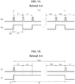
- FIG. 1A is a timing chart showing a gate voltage and a pixel voltage of an LCD device driven by a normal driving method according to the related art
- FIG. 1B is a timing chart showing a gate voltage and a pixel voltage of an LCD device driven by a low refresh rate driving method according to the related art.
- a gate voltage Vgn has a high level in each of first to sixtieth frames F1 to F60 constituting one second, and a data voltage is applied to a pixel of a display panel according to the gate voltage Vgn.
- the data voltages having opposite polarities are applied to the pixel by every two frames to be maintained as a pixel voltage Vpn for one frame.
- the gate voltage Vgn has a high level during a normal charging period CPn such that a data voltage of a positive polarity (+) or a negative polarity (-) is alternately applied to the pixel, and the pixel voltage Vpn of a positive polarity (+) or a negative polarity (-) is maintained during a normal holding period HPn to display an image.
- the normal charging period CPn corresponds to a time interval obtained by dividing about 16.7 msec of one frame by a number of pixels in a vertical pixel column
- the normal holding period HPn corresponds to a time interval obtained by subtracting the normal charging period CPn from about 16.7 msec of one frame.
- the normal charging period CPn and the normal holding period HPn are about 15.5 ⁇ sec and about 16.68 msec, respectively.
- a gate voltage Vg1 when an LCD device is driven with a frequency of about 1Hz, a gate voltage Vg1 has a high level in one of first to sixtieth frames F1 to F60 constituting one second, and a data voltage is applied to a pixel of a display panel according to the gate voltage Vg1.
- the data voltages having opposite polarities are applied to the pixel by every sixty frames to be maintained as a pixel voltage Vpl for sixty frames.
- the gate voltage Vg1 has a high level during a low refresh rate charging period CP1 such that a data voltage of a positive polarity (+) or a negative polarity (-) is alternately applied to the pixel, and the pixel voltage Vpl of a positive polarity (+) or a negative polarity (-) is maintained during a low refresh rate holding period HP1 to display an image.
- the low refresh rate charging period CP1 corresponds to a time interval obtained by dividing about 16.7 msec of one frame by a number of pixels in a vertical pixel column
- the low refresh rate holding period HP1 corresponds to a time interval obtained by subtracting the low refresh rate charging period CP1 from about 16.7 msec of one frame.
- the low refresh rate charging period CP1 and the low refresh rate holding period HP1 are about 15.5 ⁇ sec and about 1 sec, respectively.
- the pixel In the LCD device driven by the low refresh rate driving method, the pixel is charged up by the data voltage supplied once per one second corresponding to the sixty frames, and the pixel voltage Vpl is maintained without an additional supply of the data voltage for most of one second corresponding to the sixty frames to display an image such as a static image having a relatively small change in gray level between frames. As a result, its power consumption can be reduced.
- the LCD device driven by the low refresh rate driving method may have visual artifacts such as a flicker as compared with the LCD device driven by the normal driving method.
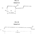
- FIG. 2A is a timing chart showing a pixel voltage of an LCD device driven by a normal driving method according to the related art
- FIG. 2B is a timing chart showing a pixel voltage of an LCD device driven by a low refresh rate driving method according to the related art.
- a data voltage is applied to a pixel during a normal charging period CPn where a gate voltage Vgn has a high level, and the data voltage is maintained as a pixel voltage Vpn during a normal holding period HPn obtained by subtracting the normal charging period CPn from one frame.
- the pixel voltage Vpn is reduced by a normal voltage drop VDn due to a leakage current through the liquid crystal layer or the thin film transistor (TFT).
- TFT thin film transistor
- a data voltage is applied to a pixel during a low refresh rate charging period CP1 where a gate voltage Vgn has a high level, and the data voltage is maintained as a pixel voltage Vpl during a low refresh rate holding period HP1 obtained by subtracting the low refresh rate charging period CP1 from sixty frames.
- the pixel voltage Vpl is reduced by a low refresh rate voltage drop VD1 due to a leakage current through the liquid crystal layer or the thin film transistor (TFT).
- TFT thin film transistor
- the low refresh rate voltage drop VD1 may cause visual artifacts such as a flicker of an image displayed by the LCD device.
- FIG. 3 is a view showing a pixel voltage and a luminance of an LCD device driven by a low refresh rate driving method according to the related art.
- a data voltage is applied to a pixel during a low refresh rate charging period CP1, and a pixel voltage Vpl is maintained without an application of the data voltage during a low refresh rate holding period HP1.
- An absolute value of the pixel voltage Vpl at a beginning of the low refresh rate holding period HP1 right after the data voltage is applied is greater than an absolute value of the pixel voltage Vpl at an end of the low refresh rate holding period HP1 right before the data voltage is applied due to a leakage current during the low refresh rate holding period HP1.
- a luminance L1 of an image displayed by the LCD device sharply increases from a low value to a high value during a period A corresponding to the low refresh rate charging period CP1 and the beginning of the low refresh rate holding period HP1.
- the period A having the sharp increase in luminance L1 may have a time of about 20 msec due to a response speed of the liquid crystal layer.
- the sharp increase in luminance L1 during a relatively short time period can be recognized as a flicker, and the display quality of the LCD device may be reduced due to such a flicker.
- a display device for low speed drive includes a display panel formed with gate lines and data lines intersecting the gate lines.
- a gate driver supplies a gate pulse to the gate lines.
- a timing controller time-divides one frame of received data into sub-frames, groups the gate lines into gate groups, controls the gate driver to scan the gate groups in scan sub-frames corresponding to a portion of the sub-frames.
- a display device for low speed drive includes a display panel including gate lines, data lines and pixels.
- a gate driver supplies a gate pulse to the gate lines.
- a timing controller time-divides one frame of received data into sub-frames, groups the gate lines into gate groups, controls an operation of the gate driver in each of the sub-frames to complete a scan operation of a corresponding gate group during a scan period of each sub-frame and cuts off a driving power source applied to buffers of the source driver.
- the present invention is directed to a display device and a method of driving the same that substantially obviate one or more problems due to limitations and disadvantages of the related art.
- An advantage of the present invention is to provide a display device with improved display quality and reduced power consumption.
- FIG. 4 is a circuit diagram illustrating a liquid crystal display (LCD) device according to the first embodiment of the present disclosure.
- an LCD device 110 includes a timing controlling unit 120, a data driving unit 130, a gate driving unit 140 and a display panel 150.
- the timing controlling unit 120 generates a gate control signal GCS, a data control signal DCS and an image data RGB using an image signal IS and a plurality of timing signals such as a data enable signal DE, a horizontal synchronization signal HSY, a vertical synchronization signal VSY and a clock CLK transmitted from an external system such as a graphic card or a television system.
- the timing controlling unit 120 supplies the data control signal DCS and the image data RGB to the data driving unit 130 and supplies the gate control signal GCS to the gate driving unit 140.
- the gate control signal GCS may include a gate output enable GOE, a gate start pulse (GSP) and a gate shift clock (GSC), and the data control signal may include a source output enable (SOE), a source start pulse (SSP) and a source sampling clock (SSC).
- GOE gate output enable
- GSP gate start pulse
- GSC gate shift clock
- SOE source output enable
- SSP source start pulse
- SSC source sampling clock
- the data driving unit 130 generates a data voltage using the data control signal DCS and the image data RGB supplied by the timing controlling unit 120 and supplies the data voltage to a plurality of data lines DL1 and DL2 of the display panel 150.
- the gate driving unit 140 generates a gate voltage using the gate control signal GCS supplied by the timing controlling unit 120 and supplies the gate voltage to a plurality of gate lines GL1 and GL2 of the display panel 150.
- the display panel 150 displays an image using the data voltage supplied by the data driving unit 130 and the gate voltage supplied by the gate driving unit 140.
- the display panel 150 includes the plurality of gate lines GL1 and GL2 and the plurality of data lines DL1 and DL2 crossing each other to define a plurality of pixels P, and a thin film transistor (TFT) T is connected to the plurality of gate lines GL1 and GL2 and the plurality of data lines DL1 and DL2.
- TFT thin film transistor
- the TFT T When a high level of the gate voltage of the plurality of gate lines GL1 and GL2 is applied to the TFT T, the TFT T is turned on and the data voltage of the plurality of data lines DL1 and DL2 is transmitted to the liquid crystal capacitor Cl and the storage capacitor Cs through and the TFT T to display a gray level.
- the liquid crystal capacitor Cl includes a pixel electrode, a common electrode and a liquid crystal layer between the pixel electrode and the common electrode, and the storage capacitor Cs maintains a voltage of the pixel electrode during one frame interval.
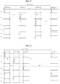
- FIG. 5 is a timing chart showing a gate voltage and a pixel voltage of an LCD device driven by a low refresh rate driving method according to the first embodiment of the present disclosure.
- an LCD device 110 when driven with a frequency of about 1Hz, one second is divided into first to sixtieth frames F1 to F60 each having about 16.7 msec, and a plurality of gate lines GL1 and GL2 are classified into first, second and third groups.
- the first group may include (3p+1)th gate lines (p is an integer equal to or greater than 0) such as the first gate line, the fourth gate line, the seventh gate line, the tenth gate line, etc.
- the second group may include (3p+2)th gate lines such as the second gate line, the fifth gate line, the eighth gate line, the eleventh gate line, etc.
- the third group may include (3p+3)th gate lines such as the third gate line, the sixth gate line, the ninth gate line and the twelfth gate line, etc.
- a gate voltage applied to the gate lines of the first, second and third groups has a high level during one of the first to sixtieth frames F1 to F60.
- the gate voltages Vg1, etc. of the high level may be sequentially applied to the (3p+1)th gate lines of the first group during the first frame F1
- the gate voltages Vg2, etc. of the high level may be sequentially applied to the (3p+2)th gate lines of the second group during the twenty-first frame F21
- the gate voltages Vg3, etc. of the high level may be sequentially applied to the (3p+3)th gate lines of the third group during the forty-first frame F41.
- the first, twenty-first and forty-first frames F1, F21 and F41 may be selected from the first to sixtieth frames F1 to F60.
- the first gate voltage Vg1, the fourth gate voltage Vg4, the seventh gate voltage Vg7, the tenth gate voltage Vg10, etc. of the high level may be sequentially applied to the first gate line GL1, the fourth gate line GL4, the seventh gate line GL7, the tenth gate line GL10, etc. of the first group.
- the second gate voltage Vg2 the fifth gate voltage Vg5, the eighth gate voltage Vg8, the eleventh gate voltage Vg11, etc.
- the third gate voltage Vg3, the sixth gate voltage Vg6, the ninth gate voltage Vg9, the twelfth gate voltage Vg12, etc. of the high level may be sequentially applied to the third gate line GL3, the sixth gate line GL6, the ninth gate line GL9, the twelfth gate line GL12, etc. of the third group.
- the data voltages may be sequentially applied to the pixels P corresponding to the gate lines GL1, GL4, GL7, GL10, etc. of the first group during charging periods CP1, CP4, CP7, CP10, etc. of the first frame F1.
- the data voltages may be sequentially applied to the pixels P corresponding to the gate lines GL2, GL5, GL8, GL11, etc. of the second group during charging periods CP2, CP5, CP8, CP11, etc. of the twenty-first frame F21.
- the data voltages may be sequentially applied to the pixels P corresponding to the gate lines GL3, GL6, GL9, GL12, etc. of the third group during charging periods CP3, CP6, CP9, CP12, etc. of the forty-first frame F41.
- the data voltages having opposite polarities may be applied to the pixel by every sixty frames to be maintained as a pixel voltage Vp for sixty frames.
- the gate voltages Vg1, Vg4, Vg7, Vg10, etc. corresponding to the first group may sequentially have the high level, and the data voltages having a positive polarity (+) or a negative polarity (-) may be alternately applied to a horizontal pixel row.
- the pixel voltages Vp1, Vp4, Vp7, Vp10, etc. having the positive polarity (+) or the negative polarity (-) may be maintained during the holding periods HP1, HP4, HP7, HP10, etc. of the first to sixtieth frames F1 to F60.
- the gate voltages Vg2, Vg5, Vg8, Vg11, etc. corresponding to the second group may sequentially have the high level, and the data voltages having a positive polarity (+) or a negative polarity (-) may be alternately applied to the horizontal pixel row.
- the pixel voltages Vp2, Vp5, Vp8, Vp11, etc. having the positive polarity (+) or the negative polarity (-) may be maintained during the holding periods HP2, HP5, HP8, HP11, etc. of the first to sixtieth frames F1 to F60.
- the gate voltages Vg3, Vg6, Vg9, Vg12, etc. corresponding to the third group may sequentially have the high level, and the data voltages having a positive polarity (+) or a negative polarity (-) may be alternately applied to the horizontal pixel row.
- the pixel voltages Vp3, Vp6, Vp9, Vp12, etc. having the positive polarity (+) or the negative polarity (-) may be maintained during the holding periods HP3, HP6, HP9, HP12, etc. of the first to sixtieth frames F1 to F60.
- the power consumption is reduced due to the low refresh rate driving method.
- the plurality of gate lines are classified into the first, second and third groups, and the data voltages are applied to the horizontal pixel row corresponding to the first, second and third groups during the first, twenty-first and forty-first frames, respectively, which are spaced apart from each other with an equal time interval.
- an increase in luminance of the LCD device 110 right after the data voltage is applied may be reduced to about 1/3 of that of the LCD device according to the related art where the data voltage is applied to all of horizontal pixel rows during one frame. Accordingly, visual artifacts such as a flicker may be reduced or prevented, thereby improving the display quality of the LCD device 110.
- the luminance increases during the first, twenty-first and forty-first frames F1, F21 and F41, and each of the first, twenty-first and forty-first frames F1, F21 and F41 has about 20 msec.
- visual artifacts such as a flicker may be reduced due to reduction of increase in luminance as compared with the LCD device according to the related art, a flicker may be recognized because the increase in luminance has a relatively short period. In another embodiment, such a flicker may be further reduced or prevented by extending the period during which the luminance increases.
- FIG. 6 is a timing chart showing a gate voltage and a pixel voltage of an LCD device driven by a low refresh rate driving method according to the second embodiment of the present disclosure.
- An LCD device according to the second embodiment has the same structure as the LCD device according to the first embodiment.
- an LCD device when driven with a frequency of about 1Hz, one second is divided into first to sixtieth frames F1 to F60 each having about 16.7 msec, and a plurality of gate lines GL1 and GL2 are classified into first, second and third groups.
- the first group may include (3p+1)th gate lines (p is an integer equal to or greater than 0) such as the first gate line, the fourth gate line, the seventh gate line, the tenth gate line, etc.
- the second group may include (3p+2)th gate lines such as the second gate line, the fifth gate line, the eighth gate line, the eleventh gate line, etc.
- the third group may include (3p+3)th gate lines such as the third gate line, the sixth gate line, the ninth gate line and the twelfth gate line, etc.
- a gate voltage applied to the gate lines of the first, second and third groups has a high level during one of the first to sixtieth frames F1 to F60.
- the gate voltages Vg1, etc. of the high level may be sequentially applied to the (3p+1)th gate lines of the first group during the first frame F1
- the gate voltages Vg2, etc. of the high level may be sequentially applied to the (3p+2)th gate lines of the second group during the (1+n)th frame F(1+n) (n is an integer equal to or greater than 1 and equal to or smaller than 5)
- the gate voltages Vg3, etc. of the high level may be sequentially applied to the (3p+3)th gate lines of the third group during the (1+2n)th frame F(1+2n).
- the gate voltages of the high level may be sequentially applied to the gate lines of the first, second and third groups during the first, second and third frames F1, F2 and F3, respectively, or the gate voltages of the high level may be sequentially applied to the gate lines of the first, third and fifth frames F1, F3 and F5, respectively.
- the gate voltages of the high level may be sequentially applied to the gate lines of the first, second and third groups during the first, fourth and seventh frames F1, F4 and F7, respectively, or the gate voltages of the high level may be sequentially applied to the gate lines of the first, fifth and ninth frames F1, F5 and F9, respectively.
- the gate voltages of the high level may be sequentially applied to the gate lines of the first, second and third groups during the first, sixth and eleventh frames F1, F6 and F11, respectively. Accordingly, the gate voltages of the high level may be applied to the gate lines of the first, second and third groups for about 33.3 msec to about 166 msec corresponding to two to ten frames.
- the first, (1+n)th and (1+2n)th frames F1, F(1+n) and F(1+2n) within ten frames may be selected from the first to sixtieth frames F1 to F60.
- the first gate voltage Vg1, the fourth gate voltage Vg4, the seventh gate voltage Vg7, the tenth gate voltage Vg10, etc. of the high level may be sequentially applied to the first gate line GL1, the fourth gate line GL4, the seventh gate line GL7, the tenth gate line GL10, etc. of the first group.
- the second gate voltage Vg2 the fifth gate voltage Vg5, the eighth gate voltage Vg8, the eleventh gate voltage Vg11, etc.
- the third gate voltage Vg3, the sixth gate voltage Vg6, the ninth gate voltage Vg9, the twelfth gate voltage Vg12, etc. of the high level may be sequentially applied to the third gate line GL3, the sixth gate line GL6, the ninth gate line GL9, the twelfth gate line GL12, etc. of the third group.
- the data voltages may be sequentially applied to the pixels P corresponding to the gate lines GL1, GL4, GL7, GL10, etc. of the first group during charging periods CP1, CP4, CP7, CP10, etc. of the first frame F1.
- the data voltages may be sequentially applied to the pixels P corresponding to the gate lines GL2, GL5, GL8, GL11, etc. of the second group during charging periods CP2, CP5, CP8, CP11, etc. of the (1+n)th frame F(1+n).
- the data voltages may be sequentially applied to the pixels P corresponding to the gate lines GL3, GL6, GL9, GL12, etc. of the third group during charging periods CP3, CP6, CP9, CP12, etc. of the (1+2n)th frame F(1+2n).
- the data voltages having opposite polarities may be applied to the pixel by every sixty frames to be maintained as a pixel voltage Vp for sixty frames.
- the gate voltages Vg1, Vg4, Vg7, Vg10, etc. corresponding to the first group may sequentially have the high level, and the data voltages having a positive polarity (+) or a negative polarity (-) may be alternately applied to a horizontal pixel row.
- the pixel voltages Vp1, Vp4, Vp7, Vp10, etc. having the positive polarity (+) or the negative polarity (-) may be maintained during the holding periods HP1, HP4, HP7, HP10, etc. of the first to sixtieth frames F1 to F60.
- the gate voltages Vg2, Vg5, Vg8, Vg11, etc. corresponding to the second group may sequentially have the high level, and the data voltages having a positive polarity (+) or a negative polarity (-) may be alternately applied to the horizontal pixel row.
- the pixel voltages Vp2, Vp5, Vp8, Vp11, etc. having the positive polarity (+) or the negative polarity (-) may be maintained during the holding periods HP2, HP5, HP8, HP11, etc. of the first to sixtieth frames F1 to F60.
- the gate voltages Vg3, Vg6, Vg9, Vg12, etc. corresponding to the third group may sequentially have the high level, and the data voltages having a positive polarity (+) or a negative polarity (-) may be alternately applied to the horizontal pixel row.
- the pixel voltages Vp3, Vp6, Vp9, Vp12, etc. having the positive polarity (+) or the negative polarity (-) may be maintained during the holding periods HP3, HP6, HP9, HP12, etc. of the first to sixtieth frames F1 to F60.
- the power consumption is reduced due to the low refresh rate driving method.
- the plurality of gate lines are classified into the first, second and third groups, and the data voltages are applied to the horizontal pixel row corresponding to the first, second and third groups during the first, (1+n)th and (1+2n)th frames, respectively, which are adjacent to each other within ten frames.
- an increase in luminance of the LCD device right after the data voltage is applied may be reduced to about 1/3 of that of the LCD device according to the related art where the data voltage is applied to all of horizontal pixel rows during one frame. Accordingly, visual artifacts such as a flicker may be reduced or prevented, thereby improving the display quality of the LCD device.
- FIG. 7 is a view showing a pixel voltage and a luminance of an LCD device driven by a low refresh rate driving method according to the second embodiment of the present disclosure.
- a data voltage is applied to a pixel during charging periods CP1, CP2, CP3, etc. of first, (1+n)th and (1+2n)th frames F1, F(1+n) and F(1+2n) (n is an integer equal to or greater than 1 and equal to or smaller than 5), and pixel voltages Vp1, Vp2, Vp3, etc. are maintained without an application of the data voltage during holding periods HP1, HP2, HP3, etc.
- the luminance of the image increases according to an application of the data voltage during the charging periods CP1, CP2, CP3, etc. of first, (1+n)th and (1+2n)th frames F1, F(1+n) and F(1+2n).
- the luminance of the image may increase by about 1/3 of an increment amount with respect to a final luminance right after the charging periods CP1, CP2, CP3, etc. due to the application of the data voltage during the first frame F1.
- the luminance of the image may increase by about 1/3 of an increment amount with respect to the final luminance right after the charging periods CP1, CP2, CP3, etc. due to the application of the data voltage during the (1+n)th frame F(1+n), and the luminance of the image may increase by about 1/3 of an increment amount with respect to the final luminance right after the charging periods CP1, CP2, CP3, etc. due to the application of the data voltage during the (1+2n)th frame F(1+2n).
- a section B where the luminance increases may have a time of about 37 msec to about 170 msec depending on a response speed of the liquid crystal layer. Since a gentle increase in luminance L having a relatively long time period may not be recognized as a flicker, the display quality of the LCD device can be improved.
- the plurality of gate lines are classified into three groups in the LCD device according to the first and second embodiments of the present disclosure
- the plurality of gate lines may be classified into various number of groups such as two groups or four groups.
- the gate voltage of the high level may be applied to the plurality of gate lines of the two groups or the four groups during two frames or four frames which are spaced apart from each other with, for example, an equal time interval.
- the gate voltage of the high level may be applied to the plurality of gate lines of the two groups or the four groups during two frames or four frames which are adjacent to each other within, for example, ten frames.
- the power consumption can be reduced and/or the display quality can be improved.
Landscapes
- Engineering & Computer Science (AREA)
- Physics & Mathematics (AREA)
- Computer Hardware Design (AREA)
- General Physics & Mathematics (AREA)
- Theoretical Computer Science (AREA)
- Chemical & Material Sciences (AREA)
- Crystallography & Structural Chemistry (AREA)
- Control Of Indicators Other Than Cathode Ray Tubes (AREA)
- Liquid Crystal Display Device Control (AREA)
Claims (4)
- Flüssigkristallanzeigevorrichtung, die Folgendes umfasst:eine Zeitvorgabesteuereinheit (120), die konfiguriert ist, ein Gate-Steuersignal (GCS), ein Datensteuersignal (DCS) und Bilddaten (RGB) unter Verwendung eines Bildsignals (IS) zu erzeugen;eine Datenansteuereinheit (130), die konfiguriert ist, unter Verwendung des Datensteuersignals (DCS) und der Bilddaten (IS) eine Datenspannung zu erzeugen;eine Gate-Ansteuereinheit (140), die konfiguriert ist, unter Verwendung des Gate-Steuersignals (GCS) eine Gate-Spannung (Vg) zu erzeugen; undeine Anzeigetafel (150), die mehrere Gate-Leitungen (GL) und mehrere Datenleitungen (DL) enthält, die einander kreuzen, um mehrere Bildpunkte (P) zu definieren, wobei die Zeitvorgabesteuereinheit (120) ausgelegt ist, die Anzeigetafel (150) mit niedriger Bildwiederholfrequenz f von 1 Hz zum Anzeigen eines Bildes mit sechzig Unterrahmen, die jeweils eine Dauer von 1/60 Sekunde aufweisen, anzusteuern,wobei die mehreren Gate-Leitungen (GL) in drei Gruppen unterteilt sind,wobei die Gate-Ansteuereinheit (140) ausgelegt ist, die Gate-Spannung (Vg) mit einem aktiven Pegel aufeinanderfolgend an die drei Gruppen der mehreren Gate-Leitungen (GL) jeweils in drei verschiedenen Unterrahmen anzulegen,wobei die drei Unterrahmen in einem Abstand von höchstens zehn Unterrahmen im ersten bis sechzigsten Unterrahmen liegen,wobei die drei Gruppen aus einer ersten, zweiten und dritten Gruppe bestehen und die drei Unterrahmen der erste, der (1 + n)-te und der (1 + 2n)-te Unterrahmen sind, wobei n eine Ganzzahl größer oder gleich 1 und kleiner oder gleich 5 ist,wobei die erste Gruppe die (3p + 1)-ten Gate-Leitungen enthält, wobei p eine Ganzzahl größer oder gleich 0 ist, wie etwa die erste Gate-Leitung, die vierte Gate-Leitung, die siebte Gate-Leitung, die zehnte Gate-Leitung, usw.,wobei die zweite Gruppe die (3p + 2)-ten Gate-Leitungen enthält, wobei p eine Ganzzahl größer oder gleich 0 ist, wie etwa die zweite Gate-Leitung, die fünfte Gate-Leitung, die achte Gate-Leitung, die elfte Gate-Leitung, usw.,wobei die dritte Gruppe die (3p + 3)-ten Gate-Leitungen enthält, wobei p eine Ganzzahl größer oder gleich 0 ist, wie etwa die dritte Gate-Leitung, die sechste Gate-Leitung, die neunte Gate-Leitung, die zwölfte-Gate-Leitung, usw.,wobei die Gate-Ansteuereinheit (140) ausgelegt ist, die Gate-Spannung mit dem aktiven Pegel während des ersten Unterrahmens aufeinanderfolgend an die Gate-Leitungen der ersten Gruppe anzulegen,wobei die Gate-Ansteuereinheit (140) ausgelegt ist, die Gate-Spannung mit dem aktiven Pegel während des (1 + n)-ten Unterrahmens aufeinanderfolgend an die Gate-Leitungen der zweiten Gruppe anzulegen, undwobei die Gate-Ansteuereinheit (140) ausgelegt ist, die Gate-Spannung mit dem aktiven Pegel während des (1 + 2n)-ten Unterrahmens aufeinanderfolgend an die Gate-Leitungen der dritten Gruppe anzulegen.
- Vorrichtung nach Anspruch 1, wobei die Datenspannung, die entweder eine positive oder eine negative Polarität aufweist, während eines ersten Ladezeitraums (CP1) des ersten Unterrahmens, in dem die Gate-Spannung mit dem hohen Pegel an die Gate-Leitungen der ersten Gruppe angelegt wird, an den Bildpunkt angelegt wird, der den Gate-Leitungen der ersten Gruppe entspricht, und eine Bildpunktspannung (Vp), die entweder die positive oder die negative Polarität aufweist, während eines ersten Haltezeitraums (HP1) des ersten bis sechzigsten Unterrahmens in dem Bildpunkt, der den Gate-Leitungen der ersten Gruppe entspricht, aufrechterhalten wird,
wobei die Datenspannung, die entweder eine positive oder eine negative Polarität aufweist, während eines zweiten Ladezeitraums (CP2) des (1 + n)-ten Unterrahmens, in dem die Gate-Spannung mit dem hohen Pegel an die Gate-Leitungen der zweiten Gruppe angelegt wird, an den Bildpunkt angelegt wird, der den Gate-Leitungen der zweiten Gruppe entspricht, und die Bildpunktspannung (Vp), die entweder die positive oder die negative Polarität aufweist, während eines zweiten Haltezeitraums (HP2) des ersten bis sechzigsten Unterrahmens in dem Bildpunkt, der den Gate-Leitungen der zweiten Gruppe entspricht, aufrechterhalten wird,
wobei die Datenspannung, die entweder eine positive oder eine negative Polarität aufweist, während eines dritten Ladezeitraums (CP3) des (1 + 2n)-ten Unterrahmens, in dem die Gate-Spannung mit dem hohen Pegel an die Gate-Leitungen der dritten Gruppe angelegt wird, an den Bildpunkt angelegt wird, der den Gate-Leitungen der dritten Gruppe entspricht, und die Bildpunktspannung (Vp), die entweder die positive oder die negative Polarität aufweist, während eines dritten Haltezeitraums (HP3) des ersten bis sechzigsten Unterrahmens in dem Bildpunkt, der den Gate-Leitungen der dritten Gruppe entspricht, aufrechterhalten wird. - Verfahren zum Ansteuern der Flüssigkristallanzeigevorrichtung nach Anspruch 1 mit niedriger Bildwiederholfrequenz f von 1 Hz durch Anzeigen eines Bildes mit sechzig Unterrahmen, die jeweils eine Dauer von 1/60 Sekunde aufweisen, wobei das Verfahren Folgendes umfasst:Erzeugen eines Gate-Steuersignals (GCS), eines Datensteuersignals (DCS) und von Bilddaten (RGB) unter Verwendung eines Bildsignals (IS);Erzeugen der Datenspannung unter Verwendung des Datensteuersignals (DCS) und der Bilddaten (IS);Erzeugen einer Gate-Spannung (Vg) unter Verwendung des Gate-Steuersignals (GCS); undaufeinanderfolgendes Anlegen der Gate-Spannung (Vg) mit einem aktiven Pegel an die drei Gruppen der mehreren Gate-Leitungen (GL) jeweils in drei verschiedenen Unterrahmen,wobei die drei Unterrahmen in einem Abstand von höchstens zehn Unterrahmen im ersten bis sechzigsten Unterrahmen liegen,wobei die drei Gruppen aus einer ersten, zweiten und dritten Gruppe bestehen und die drei Unterrahmen der erste, der (1 + n)-te und der (1 + 2n)-te Unterrahmen sind, wobei n eine Ganzzahl größer oder gleich 1 und kleiner oder gleich 5 ist,wobei die erste Gruppe die (3p + 1)-ten Gate-Leitungen enthält, wobei p eine Ganzzahl größer oder gleich 0 ist, wie etwa die erste Gate-Leitung, die vierte Gate-Leitung, die siebte Gate-Leitung, die zehnte Gate-Leitung, usw.,wobei die zweite Gruppe die (3p + 2)-ten Gate-Leitungen enthält, wobei p eine Ganzzahl größer oder gleich 0 ist, wie etwa die zweite Gate-Leitung, die fünfte Gate-Leitung, die achte Gate-Leitung, die elfte Gate-Leitung, usw.,wobei die dritte Gruppe die (3p + 3)-ten Gate-Leitungen enthält, wobei p eine Ganzzahl größer oder gleich 0 ist, wie etwa die dritte Gate-Leitung, die sechste Gate-Leitung, die neunte Gate-Leitung, die zwölfte-Gate-Leitung, usw.,wobei die Gate-Spannung mit dem aktiven Pegel während des ersten Unterrahmens aufeinanderfolgend an die Gate-Leitungen der ersten Gruppe angelegt wird,wobei die Gate-Spannung mit dem aktiven Pegel während des (1 + n)-ten Unterrahmens aufeinanderfolgend an die Gate-Leitungen der zweiten Gruppe angelegt wird, undwobei die Gate-Spannung mit dem aktiven Pegel während des (1 + 2n)-ten Unterrahmens aufeinanderfolgend an die Gate-Leitungen der dritten Gruppe angelegt wird.
- Verfahren nach Anspruch 3,
wobei die Datenspannung, die entweder eine positive oder eine negative Polarität aufweist, während eines ersten Ladezeitraums (CP1) des ersten Unterrahmens, in dem die Gate-Spannung mit dem hohen Pegel an die Gate-Leitungen der ersten Gruppe angelegt wird, an den Bildpunkt angelegt wird, der den Gate-Leitungen der ersten Gruppe entspricht, und eine Bildpunktspannung (Vp), die entweder die positive oder die negative Polarität aufweist, während eines ersten Haltezeitraums (HP1) des ersten bis sechzigsten Unterrahmens in dem Bildpunkt, der den Gate-Leitungen der ersten Gruppe entspricht, aufrechterhalten wird,
wobei die Datenspannung, die entweder eine positive oder eine negative Polarität aufweist, während eines zweiten Ladezeitraums (CP2) des (1 + n)-ten Unterrahmens, in dem die Gate-Spannung mit dem hohen Pegel an die Gate-Leitungen der zweiten Gruppe angelegt wird, an den Bildpunkt angelegt wird, der den Gate-Leitungen der zweiten Gruppe entspricht, und die Bildpunktspannung (Vp), die entweder die positive oder die negative Polarität aufweist, während eines zweiten Haltezeitraums (HP2) des ersten bis sechzigsten Unterrahmens in dem Bildpunkt, der den Gate-Leitungen der zweiten Gruppe entspricht, aufrechterhalten wird,
wobei die Datenspannung, die entweder eine positive oder eine negative Polarität aufweist, während eines dritten Ladezeitraums (CP3) des (1 + 2n)-ten Unterrahmens, in dem die Gate-Spannung mit dem hohen Pegel an die Gate-Leitungen der dritten Gruppe angelegt wird, an den Bildpunkt angelegt wird, der den Gate-Leitungen der dritten Gruppe entspricht, und die Bildpunktspannung (Vp), die entweder die positive oder die negative Polarität aufweist, während eines dritten Haltezeitraums (HP3) des ersten bis sechzigsten Unterrahmens in dem Bildpunkt, der den Gate-Leitungen der dritten Gruppe entspricht, aufrechterhalten wird.
Applications Claiming Priority (1)
| Application Number | Priority Date | Filing Date | Title |
|---|---|---|---|
| KR1020140193046A KR102281816B1 (ko) | 2014-12-30 | 2014-12-30 | 액정표시장치 및 그 구동방법 |
Publications (2)
| Publication Number | Publication Date |
|---|---|
| EP3040980A1 EP3040980A1 (de) | 2016-07-06 |
| EP3040980B1 true EP3040980B1 (de) | 2019-04-10 |
Family
ID=55027513
Family Applications (1)
| Application Number | Title | Priority Date | Filing Date |
|---|---|---|---|
| EP15202892.4A Active EP3040980B1 (de) | 2014-12-30 | 2015-12-29 | Flüssigkristallanzeigevorrichtung und verfahren zur ansteuerung davon |
Country Status (4)
| Country | Link |
|---|---|
| US (1) | US9953575B2 (de) |
| EP (1) | EP3040980B1 (de) |
| KR (1) | KR102281816B1 (de) |
| CN (1) | CN105741798B (de) |
Families Citing this family (13)
| Publication number | Priority date | Publication date | Assignee | Title |
|---|---|---|---|---|
| KR20170049735A (ko) | 2015-10-28 | 2017-05-11 | 삼성디스플레이 주식회사 | 표시 장치 |
| KR102581368B1 (ko) * | 2016-07-07 | 2023-09-22 | 삼성디스플레이 주식회사 | 표시 패널의 구동 방법 및 이를 수행하기 위한 표시 장치 |
| CN106023934B (zh) * | 2016-07-26 | 2018-07-17 | 京东方科技集团股份有限公司 | 一种显示装置及其驱动方法 |
| US10359885B2 (en) * | 2016-08-29 | 2019-07-23 | Apple Inc. | Touch induced flicker mitigation for variable refresh rate display |
| KR102556084B1 (ko) | 2016-10-07 | 2023-07-17 | 삼성디스플레이 주식회사 | 프레임 레이트를 변경할 수 있는 표시 장치 및 그것의 동작 방법 |
| CN106652878A (zh) * | 2017-02-24 | 2017-05-10 | 厦门天马微电子有限公司 | 一种显示面板的驱动方法及显示面板 |
| KR102532091B1 (ko) * | 2018-11-16 | 2023-05-15 | 엘지디스플레이 주식회사 | 표시 장치 |
| KR102647169B1 (ko) | 2019-01-14 | 2024-03-14 | 삼성디스플레이 주식회사 | 표시 장치 및 이를 이용한 표시 패널의 구동 방법 |
| KR102675755B1 (ko) * | 2019-08-08 | 2024-06-19 | 삼성디스플레이 주식회사 | 표시 장치 및 이를 이용한 표시 패널의 구동 방법 |
| KR102740427B1 (ko) * | 2019-11-28 | 2024-12-09 | 삼성디스플레이 주식회사 | 표시 장치 |
| CN111199713A (zh) | 2020-03-05 | 2020-05-26 | 苹果公司 | 具有多个刷新率模式的显示器 |
| KR102807253B1 (ko) * | 2020-03-24 | 2025-05-15 | 삼성디스플레이 주식회사 | 표시 장치 및 이를 이용한 표시 패널의 구동 방법 |
| CN115985238B (zh) * | 2023-03-22 | 2023-06-02 | 成都利普芯微电子有限公司 | 一种数据处理方法、电路及驱动芯片 |
Family Cites Families (5)
| Publication number | Priority date | Publication date | Assignee | Title |
|---|---|---|---|---|
| KR101142995B1 (ko) | 2004-12-13 | 2012-05-08 | 삼성전자주식회사 | 표시 장치 및 그 구동 방법 |
| KR20120050114A (ko) | 2010-11-10 | 2012-05-18 | 삼성모바일디스플레이주식회사 | 액정 표시 장ㅊ치 및 그 구동 방법 |
| KR102055756B1 (ko) | 2012-09-26 | 2019-12-16 | 삼성디스플레이 주식회사 | 표시 장치 및 그 구동 방법 |
| KR102050380B1 (ko) * | 2013-04-30 | 2019-11-29 | 엘지디스플레이 주식회사 | 저속 구동용 표시장치와 그 구동방법 |
| KR102035755B1 (ko) * | 2013-04-30 | 2019-11-08 | 엘지디스플레이 주식회사 | 저속 구동용 표시장치와 그 구동방법 |
-
2014
- 2014-12-30 KR KR1020140193046A patent/KR102281816B1/ko active Active
-
2015
- 2015-12-02 US US14/956,911 patent/US9953575B2/en active Active
- 2015-12-22 CN CN201510971795.5A patent/CN105741798B/zh active Active
- 2015-12-29 EP EP15202892.4A patent/EP3040980B1/de active Active
Non-Patent Citations (1)
| Title |
|---|
| None * |
Also Published As
| Publication number | Publication date |
|---|---|
| CN105741798A (zh) | 2016-07-06 |
| KR20160083178A (ko) | 2016-07-12 |
| KR102281816B1 (ko) | 2021-07-26 |
| CN105741798B (zh) | 2019-03-26 |
| US20160189616A1 (en) | 2016-06-30 |
| US9953575B2 (en) | 2018-04-24 |
| EP3040980A1 (de) | 2016-07-06 |
Similar Documents
| Publication | Publication Date | Title |
|---|---|---|
| EP3040980A1 (de) | Flüssigkristallanzeigevorrichtung und verfahren zur ansteuerung davon | |
| US11211011B2 (en) | Display device for improving display quality | |
| KR101341906B1 (ko) | 액정 표시장치의 구동장치와 그 구동방법 | |
| US9978323B2 (en) | Liquid crystal display panel and display device | |
| KR102333868B1 (ko) | Oled 표시 장치 | |
| CN100420994C (zh) | 提供数据的方法,液晶显示装置及其驱动方法 | |
| KR102279280B1 (ko) | 표시 장치 및 이의 구동 방법 | |
| CN105074808A (zh) | 显示装置及其驱动方法 | |
| KR20160073928A (ko) | 유기발광다이오드 표시장치 및 이의 구동방법 | |
| KR20190077689A (ko) | 유기 발광 다이오드 디스플레이 장치 | |
| KR102070218B1 (ko) | 표시 장치 및 그 구동 방법 | |
| KR102298337B1 (ko) | 분할 구동용 표시장치 | |
| KR102921531B1 (ko) | 표시장치와 그 구동방법 | |
| US9704450B2 (en) | Driver IC for display panel | |
| KR102147055B1 (ko) | 액정 표시 장치 및 이의 구동 방법 | |
| KR20160070446A (ko) | 표시 장치 및 표시 장치의 구동 방법 | |
| US8686936B2 (en) | Liquid crystal display apparatus and method of driving the same | |
| KR102338944B1 (ko) | 액정 표시 장치 및 그의 구동 방법 | |
| KR101630336B1 (ko) | 액정표시장치 | |
| KR102223901B1 (ko) | 표시장치 | |
| KR20130065328A (ko) | 전기영동 디스플레이 장치와 이의 구동방법 | |
| KR20130020308A (ko) | 액정패널의 구동방법 | |
| KR101915067B1 (ko) | 액정표시장치 및 그 구동방법 | |
| KR102328982B1 (ko) | 표시장치 구동 방법 | |
| KR101706233B1 (ko) | 액정 표시장치 및 그의 구동방법 |
Legal Events
| Date | Code | Title | Description |
|---|---|---|---|
| PUAI | Public reference made under article 153(3) epc to a published international application that has entered the european phase |
Free format text: ORIGINAL CODE: 0009012 |
|
| 17P | Request for examination filed |
Effective date: 20151229 |
|
| AK | Designated contracting states |
Kind code of ref document: A1 Designated state(s): AL AT BE BG CH CY CZ DE DK EE ES FI FR GB GR HR HU IE IS IT LI LT LU LV MC MK MT NL NO PL PT RO RS SE SI SK SM TR |
|
| AX | Request for extension of the european patent |
Extension state: BA ME |
|
| RBV | Designated contracting states (corrected) |
Designated state(s): AL AT BE BG CH CY CZ DE DK EE ES FI FR GB GR HR HU IE IS IT LI LT LU LV MC MK MT NL NO PL PT RO RS SE SI SK SM TR |
|
| STAA | Information on the status of an ep patent application or granted ep patent |
Free format text: STATUS: EXAMINATION IS IN PROGRESS |
|
| 17Q | First examination report despatched |
Effective date: 20170517 |
|
| GRAP | Despatch of communication of intention to grant a patent |
Free format text: ORIGINAL CODE: EPIDOSNIGR1 |
|
| STAA | Information on the status of an ep patent application or granted ep patent |
Free format text: STATUS: GRANT OF PATENT IS INTENDED |
|
| INTG | Intention to grant announced |
Effective date: 20181123 |
|
| GRAS | Grant fee paid |
Free format text: ORIGINAL CODE: EPIDOSNIGR3 |
|
| GRAA | (expected) grant |
Free format text: ORIGINAL CODE: 0009210 |
|
| STAA | Information on the status of an ep patent application or granted ep patent |
Free format text: STATUS: THE PATENT HAS BEEN GRANTED |
|
| AK | Designated contracting states |
Kind code of ref document: B1 Designated state(s): AL AT BE BG CH CY CZ DE DK EE ES FI FR GB GR HR HU IE IS IT LI LT LU LV MC MK MT NL NO PL PT RO RS SE SI SK SM TR |
|
| REG | Reference to a national code |
Ref country code: GB Ref legal event code: FG4D |
|
| REG | Reference to a national code |
Ref country code: CH Ref legal event code: EP Ref country code: AT Ref legal event code: REF Ref document number: 1119755 Country of ref document: AT Kind code of ref document: T Effective date: 20190415 |
|
| REG | Reference to a national code |
Ref country code: IE Ref legal event code: FG4D |
|
| REG | Reference to a national code |
Ref country code: DE Ref legal event code: R096 Ref document number: 602015027944 Country of ref document: DE |
|
| REG | Reference to a national code |
Ref country code: NL Ref legal event code: MP Effective date: 20190410 |
|
| REG | Reference to a national code |
Ref country code: LT Ref legal event code: MG4D |
|
| REG | Reference to a national code |
Ref country code: AT Ref legal event code: MK05 Ref document number: 1119755 Country of ref document: AT Kind code of ref document: T Effective date: 20190410 |
|
| PG25 | Lapsed in a contracting state [announced via postgrant information from national office to epo] |
Ref country code: NL Free format text: LAPSE BECAUSE OF FAILURE TO SUBMIT A TRANSLATION OF THE DESCRIPTION OR TO PAY THE FEE WITHIN THE PRESCRIBED TIME-LIMIT Effective date: 20190410 |
|
| PG25 | Lapsed in a contracting state [announced via postgrant information from national office to epo] |
Ref country code: ES Free format text: LAPSE BECAUSE OF FAILURE TO SUBMIT A TRANSLATION OF THE DESCRIPTION OR TO PAY THE FEE WITHIN THE PRESCRIBED TIME-LIMIT Effective date: 20190410 Ref country code: PT Free format text: LAPSE BECAUSE OF FAILURE TO SUBMIT A TRANSLATION OF THE DESCRIPTION OR TO PAY THE FEE WITHIN THE PRESCRIBED TIME-LIMIT Effective date: 20190910 Ref country code: LT Free format text: LAPSE BECAUSE OF FAILURE TO SUBMIT A TRANSLATION OF THE DESCRIPTION OR TO PAY THE FEE WITHIN THE PRESCRIBED TIME-LIMIT Effective date: 20190410 Ref country code: HR Free format text: LAPSE BECAUSE OF FAILURE TO SUBMIT A TRANSLATION OF THE DESCRIPTION OR TO PAY THE FEE WITHIN THE PRESCRIBED TIME-LIMIT Effective date: 20190410 Ref country code: SE Free format text: LAPSE BECAUSE OF FAILURE TO SUBMIT A TRANSLATION OF THE DESCRIPTION OR TO PAY THE FEE WITHIN THE PRESCRIBED TIME-LIMIT Effective date: 20190410 Ref country code: NO Free format text: LAPSE BECAUSE OF FAILURE TO SUBMIT A TRANSLATION OF THE DESCRIPTION OR TO PAY THE FEE WITHIN THE PRESCRIBED TIME-LIMIT Effective date: 20190710 Ref country code: AL Free format text: LAPSE BECAUSE OF FAILURE TO SUBMIT A TRANSLATION OF THE DESCRIPTION OR TO PAY THE FEE WITHIN THE PRESCRIBED TIME-LIMIT Effective date: 20190410 Ref country code: FI Free format text: LAPSE BECAUSE OF FAILURE TO SUBMIT A TRANSLATION OF THE DESCRIPTION OR TO PAY THE FEE WITHIN THE PRESCRIBED TIME-LIMIT Effective date: 20190410 |
|
| PG25 | Lapsed in a contracting state [announced via postgrant information from national office to epo] |
Ref country code: LV Free format text: LAPSE BECAUSE OF FAILURE TO SUBMIT A TRANSLATION OF THE DESCRIPTION OR TO PAY THE FEE WITHIN THE PRESCRIBED TIME-LIMIT Effective date: 20190410 Ref country code: RS Free format text: LAPSE BECAUSE OF FAILURE TO SUBMIT A TRANSLATION OF THE DESCRIPTION OR TO PAY THE FEE WITHIN THE PRESCRIBED TIME-LIMIT Effective date: 20190410 Ref country code: GR Free format text: LAPSE BECAUSE OF FAILURE TO SUBMIT A TRANSLATION OF THE DESCRIPTION OR TO PAY THE FEE WITHIN THE PRESCRIBED TIME-LIMIT Effective date: 20190711 Ref country code: PL Free format text: LAPSE BECAUSE OF FAILURE TO SUBMIT A TRANSLATION OF THE DESCRIPTION OR TO PAY THE FEE WITHIN THE PRESCRIBED TIME-LIMIT Effective date: 20190410 Ref country code: BG Free format text: LAPSE BECAUSE OF FAILURE TO SUBMIT A TRANSLATION OF THE DESCRIPTION OR TO PAY THE FEE WITHIN THE PRESCRIBED TIME-LIMIT Effective date: 20190710 |
|
| PG25 | Lapsed in a contracting state [announced via postgrant information from national office to epo] |
Ref country code: IS Free format text: LAPSE BECAUSE OF FAILURE TO SUBMIT A TRANSLATION OF THE DESCRIPTION OR TO PAY THE FEE WITHIN THE PRESCRIBED TIME-LIMIT Effective date: 20190810 Ref country code: AT Free format text: LAPSE BECAUSE OF FAILURE TO SUBMIT A TRANSLATION OF THE DESCRIPTION OR TO PAY THE FEE WITHIN THE PRESCRIBED TIME-LIMIT Effective date: 20190410 |
|
| REG | Reference to a national code |
Ref country code: DE Ref legal event code: R097 Ref document number: 602015027944 Country of ref document: DE |
|
| PG25 | Lapsed in a contracting state [announced via postgrant information from national office to epo] |
Ref country code: CZ Free format text: LAPSE BECAUSE OF FAILURE TO SUBMIT A TRANSLATION OF THE DESCRIPTION OR TO PAY THE FEE WITHIN THE PRESCRIBED TIME-LIMIT Effective date: 20190410 Ref country code: EE Free format text: LAPSE BECAUSE OF FAILURE TO SUBMIT A TRANSLATION OF THE DESCRIPTION OR TO PAY THE FEE WITHIN THE PRESCRIBED TIME-LIMIT Effective date: 20190410 Ref country code: RO Free format text: LAPSE BECAUSE OF FAILURE TO SUBMIT A TRANSLATION OF THE DESCRIPTION OR TO PAY THE FEE WITHIN THE PRESCRIBED TIME-LIMIT Effective date: 20190410 Ref country code: SK Free format text: LAPSE BECAUSE OF FAILURE TO SUBMIT A TRANSLATION OF THE DESCRIPTION OR TO PAY THE FEE WITHIN THE PRESCRIBED TIME-LIMIT Effective date: 20190410 Ref country code: DK Free format text: LAPSE BECAUSE OF FAILURE TO SUBMIT A TRANSLATION OF THE DESCRIPTION OR TO PAY THE FEE WITHIN THE PRESCRIBED TIME-LIMIT Effective date: 20190410 |
|
| PLBE | No opposition filed within time limit |
Free format text: ORIGINAL CODE: 0009261 |
|
| STAA | Information on the status of an ep patent application or granted ep patent |
Free format text: STATUS: NO OPPOSITION FILED WITHIN TIME LIMIT |
|
| PG25 | Lapsed in a contracting state [announced via postgrant information from national office to epo] |
Ref country code: SM Free format text: LAPSE BECAUSE OF FAILURE TO SUBMIT A TRANSLATION OF THE DESCRIPTION OR TO PAY THE FEE WITHIN THE PRESCRIBED TIME-LIMIT Effective date: 20190410 Ref country code: IT Free format text: LAPSE BECAUSE OF FAILURE TO SUBMIT A TRANSLATION OF THE DESCRIPTION OR TO PAY THE FEE WITHIN THE PRESCRIBED TIME-LIMIT Effective date: 20190410 |
|
| 26N | No opposition filed |
Effective date: 20200113 |
|
| PG25 | Lapsed in a contracting state [announced via postgrant information from national office to epo] |
Ref country code: TR Free format text: LAPSE BECAUSE OF FAILURE TO SUBMIT A TRANSLATION OF THE DESCRIPTION OR TO PAY THE FEE WITHIN THE PRESCRIBED TIME-LIMIT Effective date: 20190410 |
|
| PG25 | Lapsed in a contracting state [announced via postgrant information from national office to epo] |
Ref country code: SI Free format text: LAPSE BECAUSE OF FAILURE TO SUBMIT A TRANSLATION OF THE DESCRIPTION OR TO PAY THE FEE WITHIN THE PRESCRIBED TIME-LIMIT Effective date: 20190410 |
|
| REG | Reference to a national code |
Ref country code: CH Ref legal event code: PL |
|
| REG | Reference to a national code |
Ref country code: BE Ref legal event code: MM Effective date: 20191231 |
|
| PG25 | Lapsed in a contracting state [announced via postgrant information from national office to epo] |
Ref country code: MC Free format text: LAPSE BECAUSE OF FAILURE TO SUBMIT A TRANSLATION OF THE DESCRIPTION OR TO PAY THE FEE WITHIN THE PRESCRIBED TIME-LIMIT Effective date: 20190410 |
|
| PG25 | Lapsed in a contracting state [announced via postgrant information from national office to epo] |
Ref country code: IE Free format text: LAPSE BECAUSE OF NON-PAYMENT OF DUE FEES Effective date: 20191229 Ref country code: LU Free format text: LAPSE BECAUSE OF NON-PAYMENT OF DUE FEES Effective date: 20191229 |
|
| PG25 | Lapsed in a contracting state [announced via postgrant information from national office to epo] |
Ref country code: LI Free format text: LAPSE BECAUSE OF NON-PAYMENT OF DUE FEES Effective date: 20191231 Ref country code: CH Free format text: LAPSE BECAUSE OF NON-PAYMENT OF DUE FEES Effective date: 20191231 Ref country code: BE Free format text: LAPSE BECAUSE OF NON-PAYMENT OF DUE FEES Effective date: 20191231 |
|
| PG25 | Lapsed in a contracting state [announced via postgrant information from national office to epo] |
Ref country code: CY Free format text: LAPSE BECAUSE OF FAILURE TO SUBMIT A TRANSLATION OF THE DESCRIPTION OR TO PAY THE FEE WITHIN THE PRESCRIBED TIME-LIMIT Effective date: 20190410 |
|
| PG25 | Lapsed in a contracting state [announced via postgrant information from national office to epo] |
Ref country code: HU Free format text: LAPSE BECAUSE OF FAILURE TO SUBMIT A TRANSLATION OF THE DESCRIPTION OR TO PAY THE FEE WITHIN THE PRESCRIBED TIME-LIMIT; INVALID AB INITIO Effective date: 20151229 Ref country code: MT Free format text: LAPSE BECAUSE OF FAILURE TO SUBMIT A TRANSLATION OF THE DESCRIPTION OR TO PAY THE FEE WITHIN THE PRESCRIBED TIME-LIMIT Effective date: 20190410 |
|
| PG25 | Lapsed in a contracting state [announced via postgrant information from national office to epo] |
Ref country code: MK Free format text: LAPSE BECAUSE OF FAILURE TO SUBMIT A TRANSLATION OF THE DESCRIPTION OR TO PAY THE FEE WITHIN THE PRESCRIBED TIME-LIMIT Effective date: 20190410 |
|
| REG | Reference to a national code |
Ref country code: DE Ref legal event code: R082 Ref document number: 602015027944 Country of ref document: DE Representative=s name: TER MEER STEINMEISTER & PARTNER PATENTANWAELTE, DE |
|
| PGFP | Annual fee paid to national office [announced via postgrant information from national office to epo] |
Ref country code: DE Payment date: 20251020 Year of fee payment: 11 |
|
| PGFP | Annual fee paid to national office [announced via postgrant information from national office to epo] |
Ref country code: GB Payment date: 20251023 Year of fee payment: 11 |
|
| PGFP | Annual fee paid to national office [announced via postgrant information from national office to epo] |
Ref country code: FR Payment date: 20251021 Year of fee payment: 11 |