EP3038244A1 - Power conversion device and control method thereof - Google Patents
Power conversion device and control method thereof Download PDFInfo
- Publication number
- EP3038244A1 EP3038244A1 EP15199351.6A EP15199351A EP3038244A1 EP 3038244 A1 EP3038244 A1 EP 3038244A1 EP 15199351 A EP15199351 A EP 15199351A EP 3038244 A1 EP3038244 A1 EP 3038244A1
- Authority
- EP
- European Patent Office
- Prior art keywords
- cnv
- power conversion
- conversion device
- device unit
- phase
- Prior art date
- Legal status (The legal status is an assumption and is not a legal conclusion. Google has not performed a legal analysis and makes no representation as to the accuracy of the status listed.)
- Granted
Links
Images



Classifications
-
- H—ELECTRICITY
- H02—GENERATION; CONVERSION OR DISTRIBUTION OF ELECTRIC POWER
- H02M—APPARATUS FOR CONVERSION BETWEEN AC AND AC, BETWEEN AC AND DC, OR BETWEEN DC AND DC, AND FOR USE WITH MAINS OR SIMILAR POWER SUPPLY SYSTEMS; CONVERSION OF DC OR AC INPUT POWER INTO SURGE OUTPUT POWER; CONTROL OR REGULATION THEREOF
- H02M1/00—Details of apparatus for conversion
- H02M1/12—Arrangements for reducing harmonics from AC input or output
-
- H—ELECTRICITY
- H02—GENERATION; CONVERSION OR DISTRIBUTION OF ELECTRIC POWER
- H02M—APPARATUS FOR CONVERSION BETWEEN AC AND AC, BETWEEN AC AND DC, OR BETWEEN DC AND DC, AND FOR USE WITH MAINS OR SIMILAR POWER SUPPLY SYSTEMS; CONVERSION OF DC OR AC INPUT POWER INTO SURGE OUTPUT POWER; CONTROL OR REGULATION THEREOF
- H02M7/00—Conversion of AC power input into DC power output; Conversion of DC power input into AC power output
- H02M7/42—Conversion of DC power input into AC power output without possibility of reversal
- H02M7/44—Conversion of DC power input into AC power output without possibility of reversal by static converters
- H02M7/48—Conversion of DC power input into AC power output without possibility of reversal by static converters using discharge tubes with control electrode or semiconductor devices with control electrode
- H02M7/483—Converters with outputs that each can have more than two voltages levels
- H02M7/487—Neutral point clamped inverters
-
- H—ELECTRICITY
- H02—GENERATION; CONVERSION OR DISTRIBUTION OF ELECTRIC POWER
- H02M—APPARATUS FOR CONVERSION BETWEEN AC AND AC, BETWEEN AC AND DC, OR BETWEEN DC AND DC, AND FOR USE WITH MAINS OR SIMILAR POWER SUPPLY SYSTEMS; CONVERSION OF DC OR AC INPUT POWER INTO SURGE OUTPUT POWER; CONTROL OR REGULATION THEREOF
- H02M1/00—Details of apparatus for conversion
- H02M1/0003—Details of control, feedback or regulation circuits
- H02M1/0038—Circuits or arrangements for suppressing, e.g. by masking incorrect turn-on or turn-off signals, e.g. due to current spikes in current mode control
-
- H—ELECTRICITY
- H02—GENERATION; CONVERSION OR DISTRIBUTION OF ELECTRIC POWER
- H02M—APPARATUS FOR CONVERSION BETWEEN AC AND AC, BETWEEN AC AND DC, OR BETWEEN DC AND DC, AND FOR USE WITH MAINS OR SIMILAR POWER SUPPLY SYSTEMS; CONVERSION OF DC OR AC INPUT POWER INTO SURGE OUTPUT POWER; CONTROL OR REGULATION THEREOF
- H02M1/00—Details of apparatus for conversion
- H02M1/0048—Circuits or arrangements for reducing losses
- H02M1/0054—Transistor switching losses
-
- Y—GENERAL TAGGING OF NEW TECHNOLOGICAL DEVELOPMENTS; GENERAL TAGGING OF CROSS-SECTIONAL TECHNOLOGIES SPANNING OVER SEVERAL SECTIONS OF THE IPC; TECHNICAL SUBJECTS COVERED BY FORMER USPC CROSS-REFERENCE ART COLLECTIONS [XRACs] AND DIGESTS
- Y02—TECHNOLOGIES OR APPLICATIONS FOR MITIGATION OR ADAPTATION AGAINST CLIMATE CHANGE
- Y02B—CLIMATE CHANGE MITIGATION TECHNOLOGIES RELATED TO BUILDINGS, e.g. HOUSING, HOUSE APPLIANCES OR RELATED END-USER APPLICATIONS
- Y02B70/00—Technologies for an efficient end-user side electric power management and consumption
- Y02B70/10—Technologies improving the efficiency by using switched-mode power supplies [SMPS], i.e. efficient power electronics conversion e.g. power factor correction or reduction of losses in power supplies or efficient standby modes
Definitions
- Embodiments described herein relate generally to a power conversion device and a control method thereof.
- a power conversion device which outputs a large amount of power converts high voltage. Therefore, it is necessary to increase the withstand voltage of the power conversion device by using a switching element that has a high withstand voltage, or by connecting in series switching elements that do not have a high withstand voltage. Furthermore, it is necessary to increase the output voltage of the power conversion device by providing the power conversion device in multistages using a transformer.
- the switching loss of the switching device is large. Therefore, in some cases, by switching the switching element only once per cycle of an output frequency (one pulse) and shifting phases, a one-pulse control for eliminating a specific harmonic is carried out.
- This one-pulse control has an advantage in that the loss caused by switching the switching element can be reduced, and the harmonic can be reduced as well.
- Pulse Width Modulation PWM
- NPC Neutral-Point-Clamped
- the object of the invention is to provide a power conversion device and a control method thereof which are capable of reducing switching loss and eliminating a specific harmonic component.
- a power conversion device including a neutral-point-clamped power conversion device unit connected to a DC power source comprising three potentials; and a control unit configured to control ON/OFF of a switching element of the power conversion device unit.
- the control unit drives the power conversion device unit by a one-pulse control, controls a phase difference of an output voltage of the power conversion device unit with respect to a reference phase of a system voltage to control an active current component of an output current of the power conversion device unit.
- the control unit controls ON/OFF of the switching element based on: (a) a phase angle for eliminating a predetermined odd-order harmonic component of an output voltage of the power conversion device unit; and (b) a sum of the reference phase and the phase difference.
- FIG. 1 shows an example of a circuit configuration of a power conversion device in the embodiment.
- This power conversion device converts a DC voltage into any voltage of any frequency and drives a three-phase (UVW phase) AC load 10 by this voltage.
- a power conversion device unit CNV U of a U phase inputs a DC voltage V DC .
- An output terminal of this power conversion device unit CNV U is connected to a U phase primary winding of a transformer TR.
- a power conversion device unit CNV V of a V phase and a power conversion device unit CNV W of a W phase also input the DC voltage V DC in common with the U phase.
- Output terminals of these power conversion device units CNV V and CNV W are connected one-on-one to a V phase primary winding and a W phase primary winding of the transformer TR.
- a control device 20 of the power conversion device units shown in FIG. 1 controls the power conversion device unit of each phase by outputting a gate command to a switching element constituting the power conversion device unit of each phase.
- FIG. 2 shows an example of a circuit configuration of the power conversion device unit CNV U in the embodiment.
- the power conversion device unit CNV U comprises eight self-arc-extinguishing shape switching elements S U1 , S U2 , S U3 , S U4 , S U5 , S U6 , S U7 , and S U8 , eight reflux diodes D U1 , D U2 , D U3 , D U4 , D U5 , D U6 , D U7 , and D U8 connected one-on-one anti-parallel to all of the switching elements, and four clamp diodes D U9 , D U10 , D U11 , and D U12 connected to mutual connection points (neutral point N) of condensers C P and C N shown in FIG. 2 .
- This power conversion device unit CNV U is an NPC full bridge power conversion device in which the above switching elements S U1 , S U2 , S U3 , and S U4 are connected in series from the high potential side to the low potential side, and the above switching elements S U5 , S U6 , S U7 , and S U8 are connected in series from the high potential side to the low potential side to construct two legs, and in which a mutual connection point of the above clamp diodes D U9 and D U10 , and a mutual connection point of the above clamp diodes DU 11 and DU 12 , are connected to the neutral point N. Furthermore, a potential difference V UA -V UB between a connection point voltage V UA of the switching elements S U2 and S U3 and a connection point voltage V UB of the switching elements S U6 and S U7 is output to the transformer TR.
- the configuration of the NPC leg will be explained in the following, giving the U phase as an example.
- clamp diode D U9 is connected between an emitter of the switching element S U1 and the neutral point N, and the clamp diode D U10 is connected between the neutral point N and an emitter of the switching element S U3 .
- An anode of the clamp diode D U9 is connected to the neutral point N, and the cathode of the clamp diode D U9 is connected to the emitter of the switching element S U1 .
- An anode of the clamp diode D U10 is connected to the emitter of the switching element S U3 , and the cathode of the clamp diode D U10 is connected to the neutral point N.
- the NPC leg of the U phase is constructed by the self-arc-extinguishing shape switching elements S U1 , S U2 , S U3 , and S U4 , the reflux diodes D U1 , D U2 , D U3 , and D U4 , and the clamp diodes D U9 and D U10 .
- the configurations of the V-phase and W-phase NPC legs are the same as the configuration of the U-phase NPC leg.
- each of the power conversion device units CNV V of the V phase and each of the power conversion device units CNV W of the W phase are the same as the configuration of the power conversion device unit CNV U of the U phase.
- the power conversion device unit CNV U has a full bridge configuration as mentioned above.
- V DC is a direct current voltage obtained by the control device 20 controlling ON/OFF of the switching elements S U1 , S U2 , S U3 , S U4 , S U5 , S U6 , S U7 , and S U8 that constitute this power conversion device unit CNV U
- the power conversion device unit CNV U is capable of outputting one of the five levels of voltage such as -V DC , -V DC /2, 0, +V DC /2, or +V DC to the transformer TR.
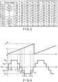
- FIG. 3 is an example of a relationship between the output voltage of the power conversion device unit CNV U , and the state of the switching elements in the embodiment.
- the ON/OFF state of the switching elements S U1 , S U2 , S U3 , S U4 , S U5 , S U6 , S U7 , and S U8 which is set for each output voltage of the power conversion device unit CNV U , comprises nine types of patterns [1], [2], [3], [4], [5], [6], [7], [8], and [9].
- switching patterns there are three types of switching patterns, such as [4], [5], and [6], in which the output voltage becomes 0, two types of switching patterns, such as [2] and [3], for +V DC /2, and two types of switching patterns, such as [7] and [8], for -V DC /2, which have redundancy.
- control device 20 determines the switching pattern for suppressing the neutral point potential fluctuations of the NPC power conversion device unit.
- the direction in which the neutral point potential fluctuates is determined by the leg connected to the neutral point N and the direction of the primary winding current I U of the transformer TR.
- the control device 20 When the output voltage is 0, there are three types of switching patterns, such as [4], [5], and [6]. However, the control device 20 always selects switching pattern [5] so that by changing the ON/OFF state of a pair of (two) switching elements, the switching pattern can be shifted to one of [2], [3], [7], and [8].
- the control device 20 needs to switch only a pair of switching elements formed by SU 1 and SU 3 .
- the control device 20 would need to switch the switching elements of the three pairs of SU 1 and SU 3 , SU 2 and SU 4 , and SU 6 and SU 8 .
- control device 20 needs to turn the switching element ON/OFF for only one pair in order to shift the switching pattern from [5] to one of [2], [3], [7], and [8], the number of times of switching can be minimized.
- phase 0 to n the output waveforms are bilaterally symmetric, and in phases n to 2n, the output waveforms are also bilaterally symmetric.
- the magnitude of the harmonic amplitude is determined by rising phases ⁇ 1 and ⁇ 2 of each voltage level allocated to each of the two legs mentioned above. Therefore, the latitude for determining the magnitude of the harmonic amplitude, that is, the adjustable phase, is the two phases of ⁇ 1 and ⁇ 2 .
- FIG. 4 shows an example of the relationship between the power conversion device unit CNV U and the phases in the embodiment.
- phase ⁇ 1 and ⁇ 2 are determined as values eliminating the fifth-order and seventh-order harmonics by the above formulas (1) and (2), the voltage utilization rate M is a fixed value. Therefore, the amplitude of the output voltage cannot be controlled in order to control the output current of the power conversion device unit.
- the three-phase output current is divided into an active current component and a reactive current component.
- FIG. 5 is a block diagram showing a function configuration example of the control device of the power conversion device in the embodiment.
- the control device 20 comprises a subtractor 21, a current controller 22, a phase operation part 23, an adder 24, and a gate generator 25.
- the subtractor 21 outputs to the current controller 22 the difference between an active current command value I P * of the three-phase output current of the power conversion device unit and an active current component value I P of the output current of the power conversion device unit.
- the current controller 22 comprises operation units 22a and 22b for performing proportional-integral control (PI control), and an adder 22c.
- PI control proportional-integral control
- adder 22c adder
- the operation unit 22a outputs to the adder 22c a value obtained by adding a feedback gain K P to the value output from the subtractor 21.
- the operation unit 22b outputs a value obtained by integrating the value output from the subtractor 21 and adding a feedback gain K i thereto to the adder 22c.
- the adder 22c outputs to the phase operation part 23 the sum of the output value received from the operation unit 22a and the output value received from the operation unit 22b.
- the phase operation part 23 computes an arc sine of the output value received from the adder 22c to compute a phase difference ⁇ * of the output voltage of the power conversion device unit with respect to a reference phase ⁇ S of a system voltage.
- the adder 24 outputs the sum of the reference phase ⁇ S of the system voltage and a phase difference ⁇ * of the output voltage of the power conversion device unit with respect to this reference phase ⁇ S to the gate generator 25.
- the gate generator 25 generates a gate control signal to be sent to the switching element of the power conversion device unit based on the output value received from the adder 24 and the phases ⁇ 1 and ⁇ 2 , and outputs it to the switching element.
- the active current component I P of the output current of the power conversion device unit can be controlled.
- FIG. 6 is a flowchart showing an example of a switching method for controlling the neutral point potential fluctuations using the power conversion device in the embodiment.
- FIG. 6 shows a switching method carried out by the control device 20 for controlling neutral point potential fluctuations when the power conversion device unit outputs -V DC /2 or +V DC /2 as an output voltage.
- the potential of the condenser C P is V P
- the potential of the condenser C N is V N
- the direction in which an output current I U is fed (current direction) from the power conversion device unit to the transformer TR is a positive direction.
- the control device 20 selects switching pattern [7] when intending to output voltage -V DC /2, and selects switching pattern [2] when intending to output voltage +V DC /2, the current is fed in a direction in which the potential V N nears the potential V P , which allows the neutral point potential fluctuations to be suppressed (S5).
- the output voltage V U is not ⁇ V DC /2 (NO in S1)
- the control device 20 should select switching pattern [5], when intending to output voltage +V DC , the control device 20 should select switching pattern [1], and when intending to output -V DC , the control device 20 should select switching pattern [9].
- phase ⁇ 1 is given as a threshold value to a leg comprising switching elements S U1 , S U2 , S U5 , and S U4
- phase ⁇ 2 is given as a threshold value to a leg comprising switching elements S U5 , S U6 , S U7 , and S U8 .
- phase ⁇ 2 is given as a threshold value to a leg comprising switching elements S U1 , S U2 , S U3 , and S U4
- phase ⁇ 1 is given as a threshold value to a leg comprising switching elements S U5 , S U6 , S U7 , and S U8 .
- control device 20 determines the switching pattern of the power conversion device unit CNV U in accordance with the magnitude of the potential V P and the potential V N , and the direction of the output current I U .
- FIG. 7 shows an example of a timing chart of the switching element state and an output voltage of the power conversion device unit CNV U in the embodiment.
- FIG. 7 shows a switching pattern and a timing chart of a DC winding voltage V U21 of the power conversion device unit CNV U .
- the power conversion device unit CNV U outputs voltages of rising phases ⁇ 1 and ⁇ 2 to the transformer TR.
- FIG. 7 shows switching patterns of S U1 , S U4 , S U5 , and S U8 . Since S U2 , S U3 , S U6 , and S U7 carry out switching complementary with respect to the above elements, the switching patterns thereof are not shown in FIG. 7 .
- the state of the switching elements with respect to voltage V U21 is indicated by [1], [2], [3], [4], [5], [6], [7], [8], and [9].
- a voltage with less low-order harmonics can be obtained by a one-pulse control in a single phase NPC power conversion device unit.
- the voltage utilization rate M is a fixed value
- current control becomes possible.
- one-pulse control since one-pulse control is applied, the number of times of switching of the power conversion device unit can be suppressed, and switching loss can be reduced.
Landscapes
- Engineering & Computer Science (AREA)
- Power Engineering (AREA)
- Inverter Devices (AREA)
Description
- Embodiments described herein relate generally to a power conversion device and a control method thereof.
- A power conversion device which outputs a large amount of power converts high voltage. Therefore, it is necessary to increase the withstand voltage of the power conversion device by using a switching element that has a high withstand voltage, or by connecting in series switching elements that do not have a high withstand voltage. Furthermore, it is necessary to increase the output voltage of the power conversion device by providing the power conversion device in multistages using a transformer.
- In the case where the withstand voltage of the switching device is high, the switching loss of the switching device is large. Therefore, in some cases, by switching the switching element only once per cycle of an output frequency (one pulse) and shifting phases, a one-pulse control for eliminating a specific harmonic is carried out. This one-pulse control has an advantage in that the loss caused by switching the switching element can be reduced, and the harmonic can be reduced as well.
- When applying Pulse Width Modulation (PWM) control to a Neutral-Point-Clamped (NPC) power conversion device, a harmonic component can be significantly reduced since the output voltage becomes even closer to the sine wave. However, in the case of using this power conversion device with a large amount of power, the loss caused by switching the switching element becomes greater.
- The object of the invention is to provide a power conversion device and a control method thereof which are capable of reducing switching loss and eliminating a specific harmonic component.
- In general, according to one embodiment, there is provided a power conversion device, including a neutral-point-clamped power conversion device unit connected to a DC power source comprising three potentials; and a control unit configured to control ON/OFF of a switching element of the power conversion device unit. The control unit drives the power conversion device unit by a one-pulse control, controls a phase difference of an output voltage of the power conversion device unit with respect to a reference phase of a system voltage to control an active current component of an output current of the power conversion device unit. The control unit controls ON/OFF of the switching element based on: (a) a phase angle for eliminating a predetermined odd-order harmonic component of an output voltage of the power conversion device unit; and (b) a sum of the reference phase and the phase difference.
- The invention can be more fully understood from the following detailed description when taken in conjunction with the accompanying drawings, in which:
-
FIG. 1 shows an example of a circuit configuration of a power conversion device in the embodiment; -
FIG. 2 shows an example of a circuit configuration of the power conversion device unit CNVU in the embodiment; -
FIG. 3 is an example of a relationship between the output voltage of the power conversion device unit CNVU, and the state of the switching elements in the embodiment; -
FIG. 4 shows an example of the relationship between the power conversion device unit CNVU and the phases in the embodiment; -
FIG. 5 is a block diagram showing a function configuration example of the control device of the power conversion device in the embodiment; -
FIG. 6 is a flowchart showing an example of a switching method for controlling the neutral point potential fluctuations using the power conversion device in the embodiment; and -
FIG. 7 shows an example of a timing chart of the switching element state and an output voltage of the power conversion device unit CNVU in the embodiment. - Embodiments will be explained below with reference to the accompanying drawings.
-
FIG. 1 shows an example of a circuit configuration of a power conversion device in the embodiment. This power conversion device converts a DC voltage into any voltage of any frequency and drives a three-phase (UVW phase)AC load 10 by this voltage. - A power conversion device unit CNVU of a U phase inputs a DC voltage VDC. An output terminal of this power conversion device unit CNVU is connected to a U phase primary winding of a transformer TR.
- A power conversion device unit CNVV of a V phase and a power conversion device unit CNVW of a W phase also input the DC voltage VDC in common with the U phase. Output terminals of these power conversion device units CNVV and CNVW are connected one-on-one to a V phase primary winding and a W phase primary winding of the transformer TR.
- Based on a voltage command value, and a voltage value, a current value, and a phase of each unit, a
control device 20 of the power conversion device units shown inFIG. 1 controls the power conversion device unit of each phase by outputting a gate command to a switching element constituting the power conversion device unit of each phase. - A detailed configuration of the power conversion device unit of each phase will be explained giving the U phase as an example.
FIG. 2 shows an example of a circuit configuration of the power conversion device unit CNVU in the embodiment. - As shown in
FIG. 1 , on a direct current side of the power conversion device unit, a condenser CP on a high potential side and a condenser CN on a low potential side are connected in series. The power conversion device unit CNVU comprises eight self-arc-extinguishing shape switching elements SU1, SU2, SU3, SU4, SU5, SU6, SU7, and SU8, eight reflux diodes DU1, DU2, DU3, DU4, DU5, DU6, DU7, and DU8 connected one-on-one anti-parallel to all of the switching elements, and four clamp diodes DU9, DU10, DU11, and DU12 connected to mutual connection points (neutral point N) of condensers CP and CN shown inFIG. 2 . - This power conversion device unit CNVU is an NPC full bridge power conversion device in which the above switching elements SU1, SU2, SU3, and SU4 are connected in series from the high potential side to the low potential side, and the above switching elements SU5, SU6, SU7, and SU8 are connected in series from the high potential side to the low potential side to construct two legs, and in which a mutual connection point of the above clamp diodes DU9 and DU10, and a mutual connection point of the above clamp diodes DU11 and DU12, are connected to the neutral point N. Furthermore, a potential difference VUA-VUB between a connection point voltage VUA of the switching elements SU2 and SU3 and a connection point voltage VUB of the switching elements SU6 and SU7 is output to the transformer TR.
- The configuration of the NPC leg will be explained in the following, giving the U phase as an example.
- In the NPC leg of the U phase, four self-arc-extinguishing shape switching elements SU1, SU2, SU3, and SU4 are connected in series from the high potential side to the low potential side, and the reflux diodes DU1, DU2, DU3, and DU4 are connected one-on-one anti-parallel to these switching elements.
- Furthermore, the clamp diode DU9 is connected between an emitter of the switching element SU1 and the neutral point N, and the clamp diode DU10 is connected between the neutral point N and an emitter of the switching element SU3. An anode of the clamp diode DU9 is connected to the neutral point N, and the cathode of the clamp diode DU9 is connected to the emitter of the switching element SU1. An anode of the clamp diode DU10 is connected to the emitter of the switching element SU3, and the cathode of the clamp diode DU10 is connected to the neutral point N.
- An emitter of the switching element SU2 and a collector of the switching element SU3 are connected to a U phase primary winding terminal of the transformer TR. An emitter of the switching element SU6 and a collector of the switching element SU7 are connected to the U phase primary winding terminal of the transformer TR. In this manner, the NPC leg of the U phase is constructed by the self-arc-extinguishing shape switching elements SU1, SU2, SU3, and SU4, the reflux diodes DU1, DU2, DU3, and DU4, and the clamp diodes DU9 and DU10. The configurations of the V-phase and W-phase NPC legs are the same as the configuration of the U-phase NPC leg.
- The configurations of each of the power conversion device units CNVV of the V phase and each of the power conversion device units CNVW of the W phase are the same as the configuration of the power conversion device unit CNVU of the U phase.
- The operation of the embodiment constructed in the above manner will be explained in detail.
- Here, the voltage output method by a single power conversion device unit will be explained, giving the power conversion device unit CNVU of the U phase as an example.
- The power conversion device unit CNVU has a full bridge configuration as mentioned above. When VDC is a direct current voltage obtained by the
control device 20 controlling ON/OFF of the switching elements SU1, SU2, SU3, SU4, SU5, SU6, SU7, and SU8 that constitute this power conversion device unit CNVU, the power conversion device unit CNVU is capable of outputting one of the five levels of voltage such as -VDC, -VDC/2, 0, +VDC/2, or +VDC to the transformer TR. -
FIG. 3 is an example of a relationship between the output voltage of the power conversion device unit CNVU, and the state of the switching elements in the embodiment. - As shown in
FIG. 3 , the ON/OFF state of the switching elements SU1, SU2, SU3, SU4, SU5, SU6, SU7, and SU8, which is set for each output voltage of the power conversion device unit CNVU, comprises nine types of patterns [1], [2], [3], [4], [5], [6], [7], [8], and [9]. - When SU1 is ON, SU3 is OFF; SU4 is ON, SU2 is OFF; SU5 is ON, SU7 is OFF; and SU8 is ON, SU6 is OFF. In this manner, each of the plurality of switching elements in the same leg operates complementarily.
- There are three types of switching patterns, such as [4], [5], and [6], in which the output voltage becomes 0, two types of switching patterns, such as [2] and [3], for +VDC/2, and two types of switching patterns, such as [7] and [8], for -VDC/2, which have redundancy.
- By utilizing this redundancy, the
control device 20 determines the switching pattern for suppressing the neutral point potential fluctuations of the NPC power conversion device unit. - When one of the two legs of the power conversion device unit is connected to the neutral point N and the other is not, that is, when one of the condensers CP and CN is included in the current path but the other is not, the neutral point potential fluctuates.
- In other words, when the output voltage is +VDC/2 (switching patterns [2], [3]) or -VDC/2 (switching patterns [7], [8]), the neutral point potential fluctuates. The reason the neutral point potential fluctuates is because only one of the condensers CP and CN is charged or discharged.
- The direction in which the neutral point potential fluctuates is determined by the leg connected to the neutral point N and the direction of the primary winding current IU of the transformer TR.
- When the output voltage is -VDC or +VDC, in addition to the switching patterns being uniquely determined, the current does not flow into the neutral point N. In other words, since an identical current flows in the two condensers CP and CN, the neutral point potential does not fluctuate.
- When the output voltage is 0, there are three types of switching patterns, such as [4], [5], and [6]. However, the
control device 20 always selects switching pattern [5] so that by changing the ON/OFF state of a pair of (two) switching elements, the switching pattern can be shifted to one of [2], [3], [7], and [8]. - For example, in order to shift the switching pattern from [5] to [2] to change the output voltage from 0 to +VDC/2, the
control device 20 needs to switch only a pair of switching elements formed by SU1 and SU3. However, in order to shift the switching pattern from [6] to [2], thecontrol device 20 would need to switch the switching elements of the three pairs of SU1 and SU3, SU2 and SU4, and SU6 and SU8. - In this manner, since the
control device 20 needs to turn the switching element ON/OFF for only one pair in order to shift the switching pattern from [5] to one of [2], [3], [7], and [8], the number of times of switching can be minimized. - In accordance with the above-mentioned switching pattern, a method of outputting to the transformer TR a voltage with a reduced low-order harmonic will be explained.
- In addition to a fundamental (primary) wave, third-order, fifth-order, seventh-order, eleventh-order, thirteenth-order, seventeenth-order, nineteenth-order, twenty third-order, twenty fifth-order, and onward harmonics are superimposed on a square-wave voltage. In
phases 0 to n, the output waveforms are bilaterally symmetric, and in phases n to 2n, the output waveforms are also bilaterally symmetric. - Even harmonics do not occur when outputting such a voltage waveform from the power conversion device unit to the transformer TR. Furthermore, the third-order harmonics eliminate each other at a three-phase line voltage.
- The magnitude of the harmonic amplitude is determined by rising phases α1 and α2 of each voltage level allocated to each of the two legs mentioned above. Therefore, the latitude for determining the magnitude of the harmonic amplitude, that is, the adjustable phase, is the two phases of α1 and α2.
- The amplitude of the harmonic voltage becomes smaller as the order of harmonics increases. Therefore, if the harmonics of lower orders are eliminated, an effect of significantly improving voltage distortion can be obtained. Therefore, it is necessary to eliminate the lowest third-order harmonics in the harmonics. However, as mentioned earlier, a 3k (k is a natural number) multiple order of harmonics, in other words, orders of harmonics in multiples of three, eliminate each other by outputting to the transformer TR the three-phase line voltage in which the phase is shifted 120 degrees. Therefore, in order to eliminate the fifth-order and seventh-order harmonics, that are next in order and higher than the third-order harmonic, it is necessary to satisfy the following formulas (1) and (2).


- By the above formulas (1) and (2), α1, α2 are uniquely calculated. Here, α1 is 0.09rad, and α2 is 0.54rad.
FIG. 4 shows an example of the relationship between the power conversion device unit CNVU and the phases in the embodiment. By allocating these calculated phases α1 and α2 one-on-one to each of the two legs, a voltage in which the fifth-order and the seventh-order harmonics are eliminated in the manner shown inFIG. 4 is output from the power conversion device unit to the transformer TR. - Here, the voltage utilization rate (the ratio of basic-wave amplitude with respect to a DC input voltage) M is expressed in formula (3) below.

- Since phases α1 and α2 are determined as values eliminating the fifth-order and seventh-order harmonics by the above formulas (1) and (2), the voltage utilization rate M is a fixed value. Therefore, the amplitude of the output voltage cannot be controlled in order to control the output current of the power conversion device unit. Thus, in the present embodiment, the three-phase output current is divided into an active current component and a reactive current component.
-
FIG. 5 is a block diagram showing a function configuration example of the control device of the power conversion device in the embodiment. - As shown in
FIG. 5 , thecontrol device 20 comprises asubtractor 21, acurrent controller 22, aphase operation part 23, anadder 24, and agate generator 25. - The
subtractor 21 outputs to thecurrent controller 22 the difference between an active current command value IP* of the three-phase output current of the power conversion device unit and an active current component value IP of the output current of the power conversion device unit. - The
current controller 22 comprisesoperation units adder 22c. - The
operation unit 22a outputs to theadder 22c a value obtained by adding a feedback gain KP to the value output from thesubtractor 21. Theoperation unit 22b outputs a value obtained by integrating the value output from thesubtractor 21 and adding a feedback gain Ki thereto to theadder 22c. Theadder 22c outputs to thephase operation part 23 the sum of the output value received from theoperation unit 22a and the output value received from theoperation unit 22b. - The
phase operation part 23 computes an arc sine of the output value received from theadder 22c to compute a phase difference θ* of the output voltage of the power conversion device unit with respect to a reference phase θS of a system voltage. - The
adder 24 outputs the sum of the reference phase θS of the system voltage and a phase difference θ* of the output voltage of the power conversion device unit with respect to this reference phase θS to thegate generator 25. Thegate generator 25 generates a gate control signal to be sent to the switching element of the power conversion device unit based on the output value received from theadder 24 and the phases α1 and α2, and outputs it to the switching element. - In this manner, by controlling the phase difference θ* of the output voltage of the power conversion device unit with respect to the reference phase θS, the active current component IP of the output current of the power conversion device unit can be controlled.
- In the above manner, even in the case where the voltage utilization rate M is fixed, by applying the above phase control, the current control becomes possible in the same manner as in the case of controlling the voltage utilization rate M.
-
FIG. 6 is a flowchart showing an example of a switching method for controlling the neutral point potential fluctuations using the power conversion device in the embodiment.FIG. 6 shows a switching method carried out by thecontrol device 20 for controlling neutral point potential fluctuations when the power conversion device unit outputs -VDC/2 or +VDC/2 as an output voltage. - Here, the potential of the condenser CP is VP, the potential of the condenser CN is VN, and the direction in which an output current IU is fed (current direction) from the power conversion device unit to the transformer TR is a positive direction.
- For example, the case will be explained in which an output voltage VU of the power conversion device unit CNVU is ±VDC/2 (YES in S1), the potential VP is greater than the potential VN (YES in S3), and the current direction is positive (YES in S4).
- In this case, if the current is fed in a direction to charge the condenser CN, the potential VN will increase, allowing the neutral point potential fluctuations to be suppressed.
- At this time, if the
control device 20 selects switching pattern [7] when intending to output voltage -VDC/2, and selects switching pattern [2] when intending to output voltage +VDC/2, the current is fed in a direction in which the potential VN nears the potential VP, which allows the neutral point potential fluctuations to be suppressed (S5). In the case where the output voltage VU is not ±VDC/2 (NO in S1), when intending to output voltage zero, thecontrol device 20 should select switching pattern [5], when intending to output voltage +VDC, thecontrol device 20 should select switching pattern [1], and when intending to output -VDC, thecontrol device 20 should select switching pattern [9]. - Other examples in the case of VP>VN will be explained.
- In the case of VP>VN, and where the current direction is positive in the above manner, if the current is fed in a direction to be discharged from the condenser CP, the potential VP will be lowered, allowing the neutral point potential fluctuations to be suppressed.
- In the case of VP>VN, and where the current direction is negative (NO in S4), if the current is fed in a direction to be discharged from the condenser CP, the potential VP will be lowered, allowing the neutral point potential fluctuations to be suppressed.
- In the case of VP>VN, and where the current direction is likewise negative, if the current is fed in a direction to charge the condenser CN, the potential VN will increase, allowing the neutral point potential fluctuations to be suppressed.
- In the case of VP>VN, and where the current direction is negative as in the manner above, when intending to output voltage -VDC/2, the
control device 20 selects switching pattern [8], and when intending to output voltage +VDC/2, thecontrol device 20 selects switching pattern [3]. - An example in the case of VP<VN (NO in S3) will be explained.
- In the case of VP>VN, and where the current direction is positive in the above manner, if the current is fed in a direction to charge the condenser CP, the potential VP will increase, allowing the neutral point potential fluctuations to be suppressed.
- In the case of VP>VN, and where the current direction is likewise positive, if the current is fed in a direction to be discharged from the condenser CN, the potential VP will be lowered, allowing the neutral point potential fluctuations to be suppressed.
- In the case of VP<VN, and where the current direction is positive as in the manner above, when intending to output voltage -VDC/2, the
control device 20 selects switching pattern [8], and when intending to output voltage +VDC/2, thecontrol device 20 selects switching pattern [3] (S8). - In the case of VP<VN, and where the current direction is negative (NO in S7), if the current is fed in a direction to be discharged from the condenser CN, the potential VN will be lowered, allowing the neutral point potential fluctuations to be suppressed.
- In the case of VP<VN, and where the current direction is likewise negative, if the current is fed in a direction to charge the condenser CP, the potential VP will increase, allowing the neutral point potential fluctuations to be suppressed.
- In the case of VP<VN, and where the current direction is negative as in the manner above, when intending to output voltage -VDC/2, the
control device 20 selects switching pattern [7], and when intending to output voltage +VDC/2, thecontrol device 20 selects switching pattern [2] (S9). - The state of switching patterns [3] and [7] is such that phase α1 is given as a threshold value to a leg comprising switching elements SU1, SU2, SU5, and SU4, and phase α2 is given as a threshold value to a leg comprising switching elements SU5, SU6, SU7, and SU8.
- Likewise, the state of switching patterns [2] and [8] is such that phase α2 is given as a threshold value to a leg comprising switching elements SU1, SU2, SU3, and SU4, and phase α1 is given as a threshold value to a leg comprising switching elements SU5, SU6, SU7, and SU8.
- In other words, the allocation of phases α1 and α2 to each leg is switched between switching patterns [3] and [7], and switching patterns [2] and [8].
- In this manner, the
control device 20 determines the switching pattern of the power conversion device unit CNVU in accordance with the magnitude of the potential VP and the potential VN, and the direction of the output current IU. -
FIG. 7 shows an example of a timing chart of the switching element state and an output voltage of the power conversion device unit CNVU in the embodiment.FIG. 7 shows a switching pattern and a timing chart of a DC winding voltage VU21 of the power conversion device unit CNVU. - The power conversion device unit CNVU outputs voltages of rising phases α1 and α2 to the transformer TR.
FIG. 7 shows switching patterns of SU1, SU4, SU5, and SU8. Since SU2, SU3, SU6, and SU7 carry out switching complementary with respect to the above elements, the switching patterns thereof are not shown inFIG. 7 . - In order to correspond to the switching patterns shown in
FIG. 3 , the state of the switching elements with respect to voltage VU21 is indicated by [1], [2], [3], [4], [5], [6], [7], [8], and [9]. - Two types of switching patterns such as [2] and [3] exist for voltage +VDC/2 since the
control device 20 selects a switching pattern in accordance with the flowchart inFIG. 5 in order to suppress neutral point potential fluctuations. The same applies for the selection of the two types of switching patterns of [7] and [8] for the output voltage -VDC/2. - The operation of the above power conversion device unit CNVU is also common to the power conversion device units of other phases.
- In the manner mentioned above, by the configuration of the power conversion device unit and the control method in the present embodiment, a voltage with less low-order harmonics can be obtained by a one-pulse control in a single phase NPC power conversion device unit.
- Furthermore, even in the case where the voltage utilization rate M is a fixed value, by applying phase control, current control becomes possible. In addition, in the present embodiment, since one-pulse control is applied, the number of times of switching of the power conversion device unit can be suppressed, and switching loss can be reduced.
- While certain embodiments have been described, these embodiments have been presented by way of example only, and are not intended to limit the scope of the inventions. Indeed, the novel embodiments described herein may be embodied in a variety of other forms; furthermore, various omissions, substitutions and changes in the form of the embodiments described herein may be made without departing from the spirit of the inventions. The accompanying claims and their equivalents are intended to cover such forms or modifications as would fall within the scope and spirit of the inventions.
Claims (5)
- A power conversion device characterized by comprising:a neutral-point-clamped power conversion device unit (CNVU, CNVV, CNVW) connected to a DC power source comprising three potentials; anda control unit (20) configured to control ON/OFF of a switching element of the power conversion device unit (CNVU, CNVV, CNVW), whereinthe control unit (20)drives the power conversion device unit (CNVU, CNVV, CNVW) by a one-pulse control, controls a phase difference of an output voltage of the power conversion device unit (CNVU, CNVV, CNVW) with respect to a reference phase of a system voltage to control an active current component of an output current of the power conversion device unit (CNVU, CNVV, CNVW), and controls ON/OFF of the switching element based on:(a) a phase angle for eliminating a predetermined odd-order harmonic component of an output voltage of the power conversion device unit (CNVU, CNVV, CNVW); and(b) a sum of the reference phase and the phase difference.
- The power conversion device according to claim 1, characterized in that the phase angle for eliminating a predetermined odd-order harmonic component is a first phase angle for eliminating a fifth-order harmonic component and a second phase angle for eliminating a seventh-order harmonic component,
the first phase angle being 0.09rad, and the second phase angle being 0.54rad. - The power conversion device according to claim 1 or 2, characterized in that the control unit (20) selects a switching pattern of the switching element to suppress neutral point potential fluctuations of the power conversion device unit (CNVU, CNVV, CNVW).
- The power conversion device according to claim 1, characterized in that the power conversion device unit (CNVU, CNVV, CNVW) outputs a three-phase AC voltage, and
the phase angle for eliminating a predetermined odd-order harmonic component is a phase angle that eliminates harmonic components of a fifth-order or above of an output voltage of the power conversion device unit (CNVU, CNVV, CNVW). - A method for controlling ON/OFF of a switching element of a neutral-point-clamped power conversion device unit (CNVU, CNVV, CNVW) connected to a DC power source comprising three potentials, characterized by comprising:driving the power conversion device unit (CNVU, CNVV, CNVW) by a one-pulse control; controlling a phase difference of an output voltage of the power conversion device unit (CNVU, CNVV, CNVW) with respect to a reference phase of a system voltage to control an active current component of an output current of the power conversion device unit (CNVU, CNVV, CNVW); and controlling ON/OFF of the switching element based on:(a) a phase angle for eliminating a predetermined odd-order harmonic component of an output voltage of the power conversion device unit (CNVU, CNVV, CNVW); and(b) a sum of the reference phase and the phase difference.
Applications Claiming Priority (1)
| Application Number | Priority Date | Filing Date | Title |
|---|---|---|---|
| JP2014260441A JP6426462B2 (en) | 2014-12-24 | 2014-12-24 | Power converter and control method thereof |
Publications (2)
| Publication Number | Publication Date |
|---|---|
| EP3038244A1 true EP3038244A1 (en) | 2016-06-29 |
| EP3038244B1 EP3038244B1 (en) | 2018-03-21 |
Family
ID=54848484
Family Applications (1)
| Application Number | Title | Priority Date | Filing Date |
|---|---|---|---|
| EP15199351.6A Not-in-force EP3038244B1 (en) | 2014-12-24 | 2015-12-10 | Power conversion device and control method thereof |
Country Status (4)
| Country | Link |
|---|---|
| US (1) | US9887617B2 (en) |
| EP (1) | EP3038244B1 (en) |
| JP (1) | JP6426462B2 (en) |
| CN (1) | CN105743377B (en) |
Cited By (1)
| Publication number | Priority date | Publication date | Assignee | Title |
|---|---|---|---|---|
| KR20180074195A (en) * | 2016-12-23 | 2018-07-03 | 울산과학기술원 | Apparatus and method for controlling voltage of a multilevel converter |
Families Citing this family (3)
| Publication number | Priority date | Publication date | Assignee | Title |
|---|---|---|---|---|
| JP6265271B6 (en) * | 2014-09-11 | 2018-02-28 | 三菱電機株式会社 | Semiconductor device |
| JP6935359B2 (en) * | 2018-04-20 | 2021-09-15 | 東芝三菱電機産業システム株式会社 | Series multiplex power converter |
| JP6856099B2 (en) * | 2019-09-06 | 2021-04-07 | 株式会社明電舎 | Control device for series multiple inverter |
Citations (4)
| Publication number | Priority date | Publication date | Assignee | Title |
|---|---|---|---|---|
| US5886888A (en) * | 1995-04-27 | 1999-03-23 | Mitsubishi Denki Kabushiki Kaisha | Voltage source type power converting apparatus |
| JP2002078346A (en) * | 2000-08-29 | 2002-03-15 | Toshiba Corp | PWM control type power converter |
| JP2003143865A (en) * | 2001-10-29 | 2003-05-16 | Toshiba Transport Eng Inc | Power converter |
| US20140119068A1 (en) * | 2012-10-30 | 2014-05-01 | Kabushiki Kaisha Toshiba | Electric power converting device and electric power converting method |
Family Cites Families (27)
| Publication number | Priority date | Publication date | Assignee | Title |
|---|---|---|---|---|
| US5436819A (en) * | 1991-07-25 | 1995-07-25 | Mitsubishi Denki Kabushiki Kaisha | Apparatus for and method of compensating for an output voltage error in an inverter output |
| JP2765315B2 (en) * | 1991-11-18 | 1998-06-11 | 株式会社日立製作所 | Power conversion device and control device for electric vehicle using the same |
| JP2000287453A (en) * | 1999-03-31 | 2000-10-13 | Mitsubishi Electric Corp | Multiple power converter |
| CN100492856C (en) * | 1999-08-12 | 2009-05-27 | 株式会社安川电机 | Tri-phase neutral point clamping type PWM inventer device |
| KR100430930B1 (en) * | 2000-02-25 | 2004-05-12 | 가부시끼가이샤 도시바 | Pwm controlled power conversion device |
| WO2002039571A1 (en) * | 2000-11-11 | 2002-05-16 | Nmb (U.S.A.), Inc. | Power converter |
| JP2004222434A (en) * | 2003-01-16 | 2004-08-05 | Fuji Electric Systems Co Ltd | Control device for power converter linked to power system |
| US7573732B2 (en) * | 2007-05-25 | 2009-08-11 | General Electric Company | Protective circuit and method for multi-level converter |
| WO2010021052A1 (en) * | 2008-08-22 | 2010-02-25 | 東芝三菱電機産業システム株式会社 | Power converting apparatus |
| EP2357721B1 (en) * | 2008-11-18 | 2016-03-30 | Mitsubishi Electric Corporation | Power conversion device |
| IT1396963B1 (en) * | 2009-10-20 | 2012-12-20 | Meta System Spa | SYSTEM AND METHOD FOR THE COMPENSATION OF THE UNBALANCE OF INPUT VOLTAGES IN THE MULTILEVEL INVERTER |
| JP5411031B2 (en) * | 2010-03-12 | 2014-02-12 | 東芝三菱電機産業システム株式会社 | 3-level power converter |
| JP2012029428A (en) * | 2010-07-22 | 2012-02-09 | Fuji Electric Co Ltd | Power conversion device |
| US8441820B2 (en) * | 2010-09-29 | 2013-05-14 | General Electric Company | DC-link voltage balancing system and method for multilevel converters |
| JP5734672B2 (en) * | 2011-01-12 | 2015-06-17 | 株式会社東芝 | Semiconductor power converter |
| JP2013110815A (en) * | 2011-11-18 | 2013-06-06 | Meidensha Corp | Neutral point clamped multilevel power converter |
| CN103138594B (en) * | 2011-11-22 | 2016-03-02 | 通用电气公司 | The control system of neutral point clamped multi current transformer and control method and compensatory control unit |
| JP2013223279A (en) * | 2012-04-13 | 2013-10-28 | Toshiba Corp | Power conversion apparatus |
| JP5784235B2 (en) * | 2012-08-10 | 2015-09-24 | 三菱電機株式会社 | 3-level power converter |
| JP2014100025A (en) * | 2012-11-15 | 2014-05-29 | Toshiba Corp | Power conversion device |
| CN104798297B (en) * | 2012-11-21 | 2018-04-17 | 奥的斯电梯公司 | The more level translators of neutral-point-clamped |
| JP6289825B2 (en) * | 2013-06-28 | 2018-03-07 | 株式会社東芝 | Generator excitation device and power conversion system |
| EP3065278B1 (en) * | 2013-10-30 | 2019-08-28 | Mitsubishi Electric Corporation | Dc/dc conversion device and load drive control system |
| WO2015102049A1 (en) * | 2014-01-06 | 2015-07-09 | 東芝三菱電機産業システム株式会社 | Electric power conversion system |
| US9325252B2 (en) * | 2014-01-13 | 2016-04-26 | Rockwell Automation Technologies, Inc. | Multilevel converter systems and sinusoidal pulse width modulation methods |
| CN105099241B (en) * | 2014-04-18 | 2019-03-19 | 通用电气公司 | Controller, power conversion system and method |
| JP6342293B2 (en) * | 2014-10-20 | 2018-06-13 | 株式会社東芝 | Neutral point clamp type power converter and control method thereof |
-
2014
- 2014-12-24 JP JP2014260441A patent/JP6426462B2/en not_active Expired - Fee Related
-
2015
- 2015-12-10 EP EP15199351.6A patent/EP3038244B1/en not_active Not-in-force
- 2015-12-11 US US14/966,130 patent/US9887617B2/en not_active Expired - Fee Related
- 2015-12-24 CN CN201510983208.4A patent/CN105743377B/en not_active Expired - Fee Related
Patent Citations (4)
| Publication number | Priority date | Publication date | Assignee | Title |
|---|---|---|---|---|
| US5886888A (en) * | 1995-04-27 | 1999-03-23 | Mitsubishi Denki Kabushiki Kaisha | Voltage source type power converting apparatus |
| JP2002078346A (en) * | 2000-08-29 | 2002-03-15 | Toshiba Corp | PWM control type power converter |
| JP2003143865A (en) * | 2001-10-29 | 2003-05-16 | Toshiba Transport Eng Inc | Power converter |
| US20140119068A1 (en) * | 2012-10-30 | 2014-05-01 | Kabushiki Kaisha Toshiba | Electric power converting device and electric power converting method |
Cited By (2)
| Publication number | Priority date | Publication date | Assignee | Title |
|---|---|---|---|---|
| KR20180074195A (en) * | 2016-12-23 | 2018-07-03 | 울산과학기술원 | Apparatus and method for controlling voltage of a multilevel converter |
| KR101884094B1 (en) | 2016-12-23 | 2018-07-31 | 울산과학기술원 | Apparatus and method for controlling voltage of a multilevel converter |
Also Published As
| Publication number | Publication date |
|---|---|
| CN105743377A (en) | 2016-07-06 |
| US20160190908A1 (en) | 2016-06-30 |
| US9887617B2 (en) | 2018-02-06 |
| EP3038244B1 (en) | 2018-03-21 |
| JP6426462B2 (en) | 2018-11-21 |
| JP2016123160A (en) | 2016-07-07 |
| CN105743377B (en) | 2019-02-15 |
Similar Documents
| Publication | Publication Date | Title |
|---|---|---|
| US9780692B2 (en) | Control device of neutral-point-clamped power converter apparatus, and control method of neutral-point-clamped power converter apparatus | |
| US9001544B2 (en) | Inverter device | |
| US9184673B2 (en) | Pulse width modulation control for a multilevel converter | |
| US9595887B2 (en) | Three-phase power conversion device | |
| JP6957196B2 (en) | Power converter | |
| CN104737433B (en) | Power-converting device | |
| KR101379202B1 (en) | Balance offset control device for neutral-point voltage control in neutral point clamped converter | |
| US9419542B2 (en) | Inverter device | |
| US10218285B2 (en) | Medium voltage hybrid multilevel converter and method for controlling a medium voltage hybrid multilevel converter | |
| US20140063885A1 (en) | Power-system-interconnected inverter device | |
| US9755551B2 (en) | Power conversion device | |
| JP6117850B2 (en) | Deviation compensation method for instrument transformer | |
| EP3038244B1 (en) | Power conversion device and control method thereof | |
| JP2015220461A (en) | Deviation compensation method for instrument transformer | |
| Meraj et al. | Simplified sinusoidal pulse width modulation of cross-switched multilevel inverter | |
| JP5910333B2 (en) | 5 level power converter | |
| JP5724486B2 (en) | Multi-level power converter | |
| JP5737268B2 (en) | Power converter | |
| JP6361803B1 (en) | Multilevel inverter control device and control method | |
| Keerthana et al. | A new Multi Level DC Link inverter topology with variable frequency inverted sine carrier PWM under equal switching transition | |
| JP2023010134A (en) | power converter | |
| Corzine | Neutral-point balancing of neutral-point-clamped three-level inverter with a front end switched rectifier DC source for the full modulation range |
Legal Events
| Date | Code | Title | Description |
|---|---|---|---|
| PUAI | Public reference made under article 153(3) epc to a published international application that has entered the european phase |
Free format text: ORIGINAL CODE: 0009012 |
|
| 17P | Request for examination filed |
Effective date: 20151210 |
|
| AK | Designated contracting states |
Kind code of ref document: A1 Designated state(s): AL AT BE BG CH CY CZ DE DK EE ES FI FR GB GR HR HU IE IS IT LI LT LU LV MC MK MT NL NO PL PT RO RS SE SI SK SM TR |
|
| AX | Request for extension of the european patent |
Extension state: BA ME |
|
| GRAP | Despatch of communication of intention to grant a patent |
Free format text: ORIGINAL CODE: EPIDOSNIGR1 |
|
| STAA | Information on the status of an ep patent application or granted ep patent |
Free format text: STATUS: GRANT OF PATENT IS INTENDED |
|
| INTG | Intention to grant announced |
Effective date: 20171107 |
|
| GRAS | Grant fee paid |
Free format text: ORIGINAL CODE: EPIDOSNIGR3 |
|
| GRAA | (expected) grant |
Free format text: ORIGINAL CODE: 0009210 |
|
| STAA | Information on the status of an ep patent application or granted ep patent |
Free format text: STATUS: THE PATENT HAS BEEN GRANTED |
|
| AK | Designated contracting states |
Kind code of ref document: B1 Designated state(s): AL AT BE BG CH CY CZ DE DK EE ES FI FR GB GR HR HU IE IS IT LI LT LU LV MC MK MT NL NO PL PT RO RS SE SI SK SM TR |
|
| REG | Reference to a national code |
Ref country code: GB Ref legal event code: FG4D |
|
| REG | Reference to a national code |
Ref country code: CH Ref legal event code: EP |
|
| REG | Reference to a national code |
Ref country code: AT Ref legal event code: REF Ref document number: 982110 Country of ref document: AT Kind code of ref document: T Effective date: 20180415 |
|
| REG | Reference to a national code |
Ref country code: IE Ref legal event code: FG4D |
|
| REG | Reference to a national code |
Ref country code: DE Ref legal event code: R096 Ref document number: 602015009055 Country of ref document: DE |
|
| REG | Reference to a national code |
Ref country code: NL Ref legal event code: MP Effective date: 20180321 |
|
| PG25 | Lapsed in a contracting state [announced via postgrant information from national office to epo] |
Ref country code: NO Free format text: LAPSE BECAUSE OF FAILURE TO SUBMIT A TRANSLATION OF THE DESCRIPTION OR TO PAY THE FEE WITHIN THE PRESCRIBED TIME-LIMIT Effective date: 20180621 Ref country code: LT Free format text: LAPSE BECAUSE OF FAILURE TO SUBMIT A TRANSLATION OF THE DESCRIPTION OR TO PAY THE FEE WITHIN THE PRESCRIBED TIME-LIMIT Effective date: 20180321 Ref country code: FI Free format text: LAPSE BECAUSE OF FAILURE TO SUBMIT A TRANSLATION OF THE DESCRIPTION OR TO PAY THE FEE WITHIN THE PRESCRIBED TIME-LIMIT Effective date: 20180321 Ref country code: CY Free format text: LAPSE BECAUSE OF FAILURE TO SUBMIT A TRANSLATION OF THE DESCRIPTION OR TO PAY THE FEE WITHIN THE PRESCRIBED TIME-LIMIT Effective date: 20180321 Ref country code: HR Free format text: LAPSE BECAUSE OF FAILURE TO SUBMIT A TRANSLATION OF THE DESCRIPTION OR TO PAY THE FEE WITHIN THE PRESCRIBED TIME-LIMIT Effective date: 20180321 |
|
| REG | Reference to a national code |
Ref country code: LT Ref legal event code: MG4D |
|
| REG | Reference to a national code |
Ref country code: AT Ref legal event code: MK05 Ref document number: 982110 Country of ref document: AT Kind code of ref document: T Effective date: 20180321 |
|
| PG25 | Lapsed in a contracting state [announced via postgrant information from national office to epo] |
Ref country code: RS Free format text: LAPSE BECAUSE OF FAILURE TO SUBMIT A TRANSLATION OF THE DESCRIPTION OR TO PAY THE FEE WITHIN THE PRESCRIBED TIME-LIMIT Effective date: 20180321 Ref country code: BG Free format text: LAPSE BECAUSE OF FAILURE TO SUBMIT A TRANSLATION OF THE DESCRIPTION OR TO PAY THE FEE WITHIN THE PRESCRIBED TIME-LIMIT Effective date: 20180621 Ref country code: LV Free format text: LAPSE BECAUSE OF FAILURE TO SUBMIT A TRANSLATION OF THE DESCRIPTION OR TO PAY THE FEE WITHIN THE PRESCRIBED TIME-LIMIT Effective date: 20180321 Ref country code: SE Free format text: LAPSE BECAUSE OF FAILURE TO SUBMIT A TRANSLATION OF THE DESCRIPTION OR TO PAY THE FEE WITHIN THE PRESCRIBED TIME-LIMIT Effective date: 20180321 Ref country code: GR Free format text: LAPSE BECAUSE OF FAILURE TO SUBMIT A TRANSLATION OF THE DESCRIPTION OR TO PAY THE FEE WITHIN THE PRESCRIBED TIME-LIMIT Effective date: 20180622 |
|
| PG25 | Lapsed in a contracting state [announced via postgrant information from national office to epo] |
Ref country code: PL Free format text: LAPSE BECAUSE OF FAILURE TO SUBMIT A TRANSLATION OF THE DESCRIPTION OR TO PAY THE FEE WITHIN THE PRESCRIBED TIME-LIMIT Effective date: 20180321 Ref country code: EE Free format text: LAPSE BECAUSE OF FAILURE TO SUBMIT A TRANSLATION OF THE DESCRIPTION OR TO PAY THE FEE WITHIN THE PRESCRIBED TIME-LIMIT Effective date: 20180321 Ref country code: ES Free format text: LAPSE BECAUSE OF FAILURE TO SUBMIT A TRANSLATION OF THE DESCRIPTION OR TO PAY THE FEE WITHIN THE PRESCRIBED TIME-LIMIT Effective date: 20180321 Ref country code: NL Free format text: LAPSE BECAUSE OF FAILURE TO SUBMIT A TRANSLATION OF THE DESCRIPTION OR TO PAY THE FEE WITHIN THE PRESCRIBED TIME-LIMIT Effective date: 20180321 Ref country code: IT Free format text: LAPSE BECAUSE OF FAILURE TO SUBMIT A TRANSLATION OF THE DESCRIPTION OR TO PAY THE FEE WITHIN THE PRESCRIBED TIME-LIMIT Effective date: 20180321 Ref country code: RO Free format text: LAPSE BECAUSE OF FAILURE TO SUBMIT A TRANSLATION OF THE DESCRIPTION OR TO PAY THE FEE WITHIN THE PRESCRIBED TIME-LIMIT Effective date: 20180321 Ref country code: AL Free format text: LAPSE BECAUSE OF FAILURE TO SUBMIT A TRANSLATION OF THE DESCRIPTION OR TO PAY THE FEE WITHIN THE PRESCRIBED TIME-LIMIT Effective date: 20180321 |
|
| PG25 | Lapsed in a contracting state [announced via postgrant information from national office to epo] |
Ref country code: CZ Free format text: LAPSE BECAUSE OF FAILURE TO SUBMIT A TRANSLATION OF THE DESCRIPTION OR TO PAY THE FEE WITHIN THE PRESCRIBED TIME-LIMIT Effective date: 20180321 Ref country code: SK Free format text: LAPSE BECAUSE OF FAILURE TO SUBMIT A TRANSLATION OF THE DESCRIPTION OR TO PAY THE FEE WITHIN THE PRESCRIBED TIME-LIMIT Effective date: 20180321 Ref country code: SM Free format text: LAPSE BECAUSE OF FAILURE TO SUBMIT A TRANSLATION OF THE DESCRIPTION OR TO PAY THE FEE WITHIN THE PRESCRIBED TIME-LIMIT Effective date: 20180321 Ref country code: AT Free format text: LAPSE BECAUSE OF FAILURE TO SUBMIT A TRANSLATION OF THE DESCRIPTION OR TO PAY THE FEE WITHIN THE PRESCRIBED TIME-LIMIT Effective date: 20180321 |
|
| PG25 | Lapsed in a contracting state [announced via postgrant information from national office to epo] |
Ref country code: PT Free format text: LAPSE BECAUSE OF FAILURE TO SUBMIT A TRANSLATION OF THE DESCRIPTION OR TO PAY THE FEE WITHIN THE PRESCRIBED TIME-LIMIT Effective date: 20180723 |
|
| REG | Reference to a national code |
Ref country code: DE Ref legal event code: R097 Ref document number: 602015009055 Country of ref document: DE |
|
| PLBE | No opposition filed within time limit |
Free format text: ORIGINAL CODE: 0009261 |
|
| STAA | Information on the status of an ep patent application or granted ep patent |
Free format text: STATUS: NO OPPOSITION FILED WITHIN TIME LIMIT |
|
| PG25 | Lapsed in a contracting state [announced via postgrant information from national office to epo] |
Ref country code: DK Free format text: LAPSE BECAUSE OF FAILURE TO SUBMIT A TRANSLATION OF THE DESCRIPTION OR TO PAY THE FEE WITHIN THE PRESCRIBED TIME-LIMIT Effective date: 20180321 |
|
| 26N | No opposition filed |
Effective date: 20190102 |
|
| PG25 | Lapsed in a contracting state [announced via postgrant information from national office to epo] |
Ref country code: SI Free format text: LAPSE BECAUSE OF FAILURE TO SUBMIT A TRANSLATION OF THE DESCRIPTION OR TO PAY THE FEE WITHIN THE PRESCRIBED TIME-LIMIT Effective date: 20180321 |
|
| REG | Reference to a national code |
Ref country code: CH Ref legal event code: PL |
|
| PG25 | Lapsed in a contracting state [announced via postgrant information from national office to epo] |
Ref country code: MC Free format text: LAPSE BECAUSE OF FAILURE TO SUBMIT A TRANSLATION OF THE DESCRIPTION OR TO PAY THE FEE WITHIN THE PRESCRIBED TIME-LIMIT Effective date: 20180321 Ref country code: LU Free format text: LAPSE BECAUSE OF NON-PAYMENT OF DUE FEES Effective date: 20181210 |
|
| REG | Reference to a national code |
Ref country code: IE Ref legal event code: MM4A |
|
| REG | Reference to a national code |
Ref country code: BE Ref legal event code: MM Effective date: 20181231 |
|
| PG25 | Lapsed in a contracting state [announced via postgrant information from national office to epo] |
Ref country code: IE Free format text: LAPSE BECAUSE OF NON-PAYMENT OF DUE FEES Effective date: 20181210 Ref country code: FR Free format text: LAPSE BECAUSE OF NON-PAYMENT OF DUE FEES Effective date: 20181231 |
|
| PG25 | Lapsed in a contracting state [announced via postgrant information from national office to epo] |
Ref country code: BE Free format text: LAPSE BECAUSE OF NON-PAYMENT OF DUE FEES Effective date: 20181231 |
|
| PG25 | Lapsed in a contracting state [announced via postgrant information from national office to epo] |
Ref country code: LI Free format text: LAPSE BECAUSE OF NON-PAYMENT OF DUE FEES Effective date: 20181231 Ref country code: CH Free format text: LAPSE BECAUSE OF NON-PAYMENT OF DUE FEES Effective date: 20181231 |
|
| PG25 | Lapsed in a contracting state [announced via postgrant information from national office to epo] |
Ref country code: MT Free format text: LAPSE BECAUSE OF NON-PAYMENT OF DUE FEES Effective date: 20181210 |
|
| PG25 | Lapsed in a contracting state [announced via postgrant information from national office to epo] |
Ref country code: TR Free format text: LAPSE BECAUSE OF FAILURE TO SUBMIT A TRANSLATION OF THE DESCRIPTION OR TO PAY THE FEE WITHIN THE PRESCRIBED TIME-LIMIT Effective date: 20180321 |
|
| PG25 | Lapsed in a contracting state [announced via postgrant information from national office to epo] |
Ref country code: MK Free format text: LAPSE BECAUSE OF NON-PAYMENT OF DUE FEES Effective date: 20180321 Ref country code: HU Free format text: LAPSE BECAUSE OF FAILURE TO SUBMIT A TRANSLATION OF THE DESCRIPTION OR TO PAY THE FEE WITHIN THE PRESCRIBED TIME-LIMIT; INVALID AB INITIO Effective date: 20151210 |
|
| PG25 | Lapsed in a contracting state [announced via postgrant information from national office to epo] |
Ref country code: IS Free format text: LAPSE BECAUSE OF FAILURE TO SUBMIT A TRANSLATION OF THE DESCRIPTION OR TO PAY THE FEE WITHIN THE PRESCRIBED TIME-LIMIT Effective date: 20180721 |
|
| GBPC | Gb: european patent ceased through non-payment of renewal fee |
Effective date: 20191210 |
|
| PG25 | Lapsed in a contracting state [announced via postgrant information from national office to epo] |
Ref country code: GB Free format text: LAPSE BECAUSE OF NON-PAYMENT OF DUE FEES Effective date: 20191210 |
|
| PGFP | Annual fee paid to national office [announced via postgrant information from national office to epo] |
Ref country code: DE Payment date: 20231017 Year of fee payment: 9 |
|
| REG | Reference to a national code |
Ref country code: DE Ref legal event code: R119 Ref document number: 602015009055 Country of ref document: DE |
|
| PG25 | Lapsed in a contracting state [announced via postgrant information from national office to epo] |
Ref country code: DE Free format text: LAPSE BECAUSE OF NON-PAYMENT OF DUE FEES Effective date: 20250701 |