EP3035248A1 - Rfid tag and method for manufacturing same - Google Patents
Rfid tag and method for manufacturing same Download PDFInfo
- Publication number
- EP3035248A1 EP3035248A1 EP13891497.3A EP13891497A EP3035248A1 EP 3035248 A1 EP3035248 A1 EP 3035248A1 EP 13891497 A EP13891497 A EP 13891497A EP 3035248 A1 EP3035248 A1 EP 3035248A1
- Authority
- EP
- European Patent Office
- Prior art keywords
- rfid tag
- metal layer
- core
- folded
- layer
- Prior art date
- Legal status (The legal status is an assumption and is not a legal conclusion. Google has not performed a legal analysis and makes no representation as to the accuracy of the status listed.)
- Withdrawn
Links
Images




Classifications
-
- G—PHYSICS
- G06—COMPUTING OR CALCULATING; COUNTING
- G06K—GRAPHICAL DATA READING; PRESENTATION OF DATA; RECORD CARRIERS; HANDLING RECORD CARRIERS
- G06K19/00—Record carriers for use with machines and with at least a part designed to carry digital markings
- G06K19/06—Record carriers for use with machines and with at least a part designed to carry digital markings characterised by the kind of the digital marking, e.g. shape, nature, code
- G06K19/067—Record carriers with conductive marks, printed circuits or semiconductor circuit elements, e.g. credit or identity cards also with resonating or responding marks without active components
- G06K19/07—Record carriers with conductive marks, printed circuits or semiconductor circuit elements, e.g. credit or identity cards also with resonating or responding marks without active components with integrated circuit chips
- G06K19/0723—Record carriers with conductive marks, printed circuits or semiconductor circuit elements, e.g. credit or identity cards also with resonating or responding marks without active components with integrated circuit chips the record carrier comprising an arrangement for non-contact communication, e.g. wireless communication circuits on transponder cards, non-contact smart cards or RFIDs
-
- H—ELECTRICITY
- H01—ELECTRIC ELEMENTS
- H01Q—ANTENNAS, i.e. RADIO AERIALS
- H01Q1/00—Details of, or arrangements associated with, antennas
- H01Q1/12—Supports; Mounting means
- H01Q1/22—Supports; Mounting means by structural association with other equipment or articles
- H01Q1/2208—Supports; Mounting means by structural association with other equipment or articles associated with components used in interrogation type services, i.e. in systems for information exchange between an interrogator/reader and a tag/transponder, e.g. in Radio Frequency Identification [RFID] systems
-
- G—PHYSICS
- G06—COMPUTING OR CALCULATING; COUNTING
- G06K—GRAPHICAL DATA READING; PRESENTATION OF DATA; RECORD CARRIERS; HANDLING RECORD CARRIERS
- G06K19/00—Record carriers for use with machines and with at least a part designed to carry digital markings
- G06K19/02—Record carriers for use with machines and with at least a part designed to carry digital markings characterised by the selection of materials, e.g. to avoid wear during transport through the machine
- G06K19/022—Processes or apparatus therefor
-
- G—PHYSICS
- G06—COMPUTING OR CALCULATING; COUNTING
- G06K—GRAPHICAL DATA READING; PRESENTATION OF DATA; RECORD CARRIERS; HANDLING RECORD CARRIERS
- G06K19/00—Record carriers for use with machines and with at least a part designed to carry digital markings
- G06K19/06—Record carriers for use with machines and with at least a part designed to carry digital markings characterised by the kind of the digital marking, e.g. shape, nature, code
- G06K19/067—Record carriers with conductive marks, printed circuits or semiconductor circuit elements, e.g. credit or identity cards also with resonating or responding marks without active components
- G06K19/07—Record carriers with conductive marks, printed circuits or semiconductor circuit elements, e.g. credit or identity cards also with resonating or responding marks without active components with integrated circuit chips
- G06K19/077—Constructional details, e.g. mounting of circuits in the carrier
- G06K19/07749—Constructional details, e.g. mounting of circuits in the carrier the record carrier being capable of non-contact communication, e.g. constructional details of the antenna of a non-contact smart card
- G06K19/07773—Antenna details
- G06K19/07786—Antenna details the antenna being of the HF type, such as a dipole
-
- H—ELECTRICITY
- H01—ELECTRIC ELEMENTS
- H01Q—ANTENNAS, i.e. RADIO AERIALS
- H01Q7/00—Loop antennas with a substantially uniform current distribution around the loop and having a directional radiation pattern in a plane perpendicular to the plane of the loop
-
- H—ELECTRICITY
- H01—ELECTRIC ELEMENTS
- H01Q—ANTENNAS, i.e. RADIO AERIALS
- H01Q9/00—Electrically-short antennas having dimensions not more than twice the operating wavelength and consisting of conductive active radiating elements
- H01Q9/04—Resonant antennas
- H01Q9/06—Details
- H01Q9/065—Microstrip dipole antennas
-
- H—ELECTRICITY
- H01—ELECTRIC ELEMENTS
- H01Q—ANTENNAS, i.e. RADIO AERIALS
- H01Q9/00—Electrically-short antennas having dimensions not more than twice the operating wavelength and consisting of conductive active radiating elements
- H01Q9/04—Resonant antennas
- H01Q9/16—Resonant antennas with feed intermediate between the extremities of the antenna, e.g. centre-fed dipole
- H01Q9/28—Conical, cylindrical, cage, strip, gauze, or like elements having an extended radiating surface; Elements comprising two conical surfaces having collinear axes and adjacent apices and fed by two-conductor transmission lines
- H01Q9/285—Planar dipole
Definitions
- the present invention relates to an RFID (Radio Frequency IDentification) tag and a manufacturing method thereof.
- the RFID tag is sometimes also referred to as an IC (Integrated Circuit) tag.
- the RFID tag is used in various fields.
- a communication system between the RFID tag and a tag reader or a tag writer includes an electromagnetic induction system and a radio wave system.
- the RFID tag may be mounted on a curved surface, a metal surface, or the like.
- a core of the RFID is desirably formed by an elastic material.
- a communication distance communicable between the RFID tag and the tag reader or the tag writer can be improved by forming an antenna in a loop shape.
- the loop-shaped antenna part in a case in which when mounting the RFID tag on an inner side or an outer side of a metal pipe having a relatively small diameter, for example, it is difficult to form the loop-shaped antenna part to have a suitable elasticity, even when the core of the RFID tag is formed by the elastic material. For this reason, as a radius of curvature of the curved surface becomes smaller, wrinkles or cracks may be formed at the loop-shaped antenna part of the RFID tag, and in a worst case, the RFID tag is broken or damaged.
- the smaller the radius or curvature of the curves surface the easier the mounted RFID tag separates from the adhered curved surface, because it is difficult to form the loop-shaped antenna part to have the suitable elasticity.
- the curved surface may include a plurality of concave parts and convex parts, or a plurality of concave parts or convex parts having different radii of curvature. In these cases, it is also difficult to mount the RFID tag having the loop-shaped antenna on the curved surface.
- One object of the present invention is to provide an RFID tag having a loop-shaped antenna and suited for mounted on a curved surface, and a manufacturing method thereof.
- an RFID tag includes a core formed by a first elastic material and having a first surface, a second surface on an opposite side of the first surface, and a pair of end parts provided on mutually opposite sides and connecting to the first surface and the second surface; a first metal layer provided on the first surface; a semiconductor chip provided on the second surface and having a communication part; and a dipole antenna provided on the second surface and electrically connected to the semiconductor chip, wherein one of the first metal layer and the dipole antenna is folded at folded parts at the pair of end parts, and the first metal layer and the dipole antenna overlap at the folded parts.
- an RFID tag having a loop-shaped antenna and suited for mounting on a curved surface.
- a core is formed by an elastic material and has a first surface, a second surface on an opposite side of the first surface, and a pair of end parts provided on mutually opposite sides and connecting to the first surface and the second surface.
- a first metal layer is provided on the first surface, and a semiconductor chip provided on the second surface and has a communication part.
- a dipole antenna is provided on the second surface and is electrically connected to the semiconductor chip.
- One of the first metal layer and the dipole antenna is folded at folded parts at the pair of end parts, and the first metal layer and the dipole antenna overlap at the folded parts.
- FIG. 1 is a cross sectional view for explaining the manufacturing method of the RFID tag in the first embodiment.
- FIG. 1 and FIGs. 2 through 14 which will be described later, dimensions including thicknesses of each of layers are illustrated for easy viewing, and proportions of the dimensions including the thicknesses of each of the layers in these figures do not correspond to actual proportions of the dimensions including the thicknesses of each of the layers.
- a core 1 formed by an elastic material is prepared.
- the core 1 is formed by a plate-shaped dielectric having a thickness of 0.8 mm, for example, and has a rectangular shape in a plan view.
- the dielectric may be PVC (Poly-Vinyl Chloride), silicone rubber, or the like, for example.
- the core 1 has a flat lower surface which is an example of a first surface, and a flat upper surface which is an example of a second surface.
- the thickness of the dielectric forming the core 1 may be in a range of 0.5 mm to 1.5 mm, for example.
- An adhesive agent used for the adhesive layer 2 is not limited to a particular adhesive agent as long as the adhesive agent has elasticity after curing.
- the thickness of the adhesive layer 2 may be in a range of 0.05 mm to 0.15 mm, for example.
- a tag chip 3 which is an example of a semiconductor chip, is provided on a surface of an insulator layer 4 formed by an elastic material and formed with a pattern of a metal layer (not illustrated). The surface (lower surface in (b) of FIG. 1 ) of the insulator layer 4 provided with the pattern of the metal layer and the tag chip 3 is adhered on the adhesive layer 2.
- the pattern of the metal layer made of copper (Cu), silver (Ag), gold (Au), aluminum (Al), or the like is formed on one surface of a PET (Poly-Ethylene Terephthalate) having a thickness of 0.05 mm, for example, and a part of the tag chip 3 electrically connecting to the patterns of the metal layer has a thickness of 0.21 mm, for example.
- the pattern of the metal layer forms a dipole antenna.
- the tag chip 3 is provided at a central part of the surface of the insulator layer 4 formed with the pattern of the metal layer, and thus, in a state in which the insulator layer 4 is adhered to the adhesive layer 2, the tag chip 3 is provided at a central part of the upper surface of the core 1.
- An adhesive agent used for the adhesive layer 5 is not limited to a particular adhesive agent as long as the adhesive agent has elasticity after curing, and may be the same as the adhesive agent used for the adhesive layer 2.
- the thickness of the adhesive layer 5 may be in a range of 0.05 mm to 0.15 mm, for example.
- a metal layer 6 is adhered to the adhesive layer 5.
- the metal layer 6 is formed by a metal or alloy that is relatively soft and suited for bending, such as tin (Sn), zinc (Zn), lead (Pb), indium (In), or an alloy including at least one of these metals, and has a thickness of 0.30 mm, for example.
- a metal or alloy that is relatively soft and suited for bending such as tin (Sn), zinc (Zn), lead (Pb), indium (In), or an alloy including at least one of these metals, and has a thickness of 0.30 mm, for example.
- the metal forming the pattern of the metal layer formed on the insulator layer 4 and the metal forming the metal layer 6 are different.
- the thickness of the metal layer 6 may be in a range of 0.15 mm to 0.30 mm, for example.
- the adhesive layer 5 and the metal layer 6 are folded at both end parts of the core 1.
- the adhesive layer 5 and the metal layer 6 are once bent in a vertical direction (upward direction) along the end parts of the core 1, and are further bent in a horizontal direction (that is, in a direction towards the central part provided with the tag chip 3) along an upper surface of the insulator layer 4.
- the adhesive layer 5 and the metal layer 6 are folded in a horizontal U-shape at both end parts of the core 1. Accordingly, both end parts of the adhesive layer 5 are adhered on the upper surface of the insulator layer 4.
- the thickness of the adhesive layers 2 and 5 can be made thin because the thicknesses of the adhesive layers 2 and 5 are slightly reduced (for example, by approximately 10%) during the curing, and the thickness of the RFID tag is 1.745 mm, for example.
- a cost and a weight of the RFID tag can also be reduced.
- the metal layer 6 and the dipole antenna formed by the pattern of the metal layer on the insulator layer 4 overlap, to form a loop-shaped antenna.
- the RFID tag is mounted on a metal surface, for example, it is possible to improve a communication distance communicable between the RFID tag and a tag reader (not illustrated) or a tag writer (not illustrated).
- the folded parts of the metal layer 6 hold both ends of the insulator layer 4 or the like, even in a case in which the entire RFID tag is bent when mounting the RFID tag on a curved surface, for example, it was confirmed that the insulator layer 4, the metal layer 6, or the like of the RFID tag do not separate from the core 1, and that wrinkles or cracks are uneasily formed in the RFID tag.
- a lower surface of the RFID tag illustrated in (d) of FIG. 1 is mounted on a curved surface having a radius of curvature that is 15 mm, for example, using an adhesive tape, it was confirmed that the RFID tag is uneasily broken or damaged.
- the RFID tag is suited for mounting on the curved surface.
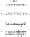
- FIG. 2 is a cross sectional view for explaining the manufacturing method of the RFID tag in the second embodiment.
- those parts that are the same as those corresponding parts in FIG. 1 are designated by the same reference numerals, and a description thereof will be omitted.
- the core 1 formed by an elastic material is prepared.
- the adhesive layer 5 is formed on the lower surface of the core 1.
- the metal layer 6 is adhered on the adhesive layer 5.
- the adhesive layer 5 and the metal layer 6 are folded at both end parts of the core 1.
- the adhesive layer 5 and the metal layer 6 are once bent in a vertical direction (upward direction) along the end parts of the core 1, and are further bent in a horizontal direction (that is, in a direction towards a central part provided with the tag chip 3) along the upper surface of the core 1.
- the adhesive layer 5 and the metal layer 6 are folded in a horizontal U-shape at both end parts of the core 1. Accordingly, both end parts of the adhesive layer 5 are adhered on the upper surface of the core 1.
- the adhesive layer 2 is formed on the upper surface of the core 1, and on an upper surface of folded parts where the metal layer 6 is folded in the horizontal U-shape at both end parts of the core 1.
- the tag chip 3 is provided on the surface of the insulator layer 4 formed by an elastic material, and formed with the pattern of the metal layer (not illustrated).
- the surface (lower surface in (d) of FIG. 2 ) of the insulator layer 4 provided with the pattern of the metal layer and the tag chip 3 is adhered on the adhesive layer 2, and formed with the pattern of the metal layer (not illustrated).
- the thickness of the adhesive layers 2 and 5 can be made thin because the thicknesses of the adhesive layers 2 and 5 are slightly reduced during the curing, and the thickness of the RFID tag is 1.745 mm, for example. In addition, the cost and the weight of the RFID tag can also be reduced. Moreover, because the insulator layer 4 is formed on the folded parts of the metal layer 6, not only the lower surface but also the upper surface of the RFID tag can be made flat.
- the metal layer 6 and the dipole antenna formed by the pattern of the metal layer on the insulator layer 4 overlap, to form a loop-shaped antenna.
- the RFID tag is mounted on a metal surface, for example, it is possible to improve the communication distance communicable between the RFID tag and the tag reader (not illustrated) or the tag writer (not illustrated).
- the folded parts of the metal layer 6 hold both ends of the core 1, the insulator layer 4, or the like, even in a case in which the entire RFID tag is bent when mounting the RFID tag on a curved surface, for example, it was confirmed that the insulator layer 4, the metal layer 6, or the like of the RFID tag do not separate from the core 1, and that wrinkles or cracks are uneasily formed in the RFID tag.
- a lower surface or an upper surface of the RFID tag illustrated in (d) of FIG. 2 is mounted on a curved surface having a radius of curvature that is 15 mm, for example, using an adhesive tape, it was confirmed that the RFID tag is uneasily broken or damaged.
- the RFID tag is suited for mounting on the curved surface.
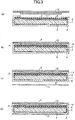
- FIG. 3 is a cross sectional view for explaining the manufacturing method of the RFID tag in the third embodiment.
- those parts that are the same as those corresponding parts in FIG. 1 are designated by the same reference numerals, and a description thereof will be omitted.
- a protection layer is formed on the upper surfaces of the insulator layer 4 and the folded parts in (d) of FIG. 1 .
- a protection layer 12 is formed on the upper surface of the RFID tag in the first embodiment illustrated in (d) of FIG. 1 , via an adhesive layer 11.
- An adhesive agent used for the adhesive layer 11 is not limited to a particular adhesive agent as long as the adhesive agent has elasticity after curing, and may be the same as the adhesive agent used for the adhesive layer 2 or the adhesive layer 5.
- a material used for the protection layer 12 is not limited to a particular material as long as the material has elasticity, and may be a flame resistant material, for example.
- the adhesive layer 11 has a thickness of 0.05 mm, for example, and the protection layer 12 has a thickness of 0.15 mm, for example.
- a combination of the adhesive layer 11 and the protection layer 12 may be a film coated with an adhesive agent, for example.
- the adhesive layer 11 may have a thickness in a range of 0.05 mm to 0.15 mm, for example.
- the protection layer 12 may have a thickness in a range of 0.05 mm to 0.15 mm, for example.
- an adhesive layer 13 is formed on a lower surface of the metal layer 6.
- An adhesive agent used for the adhesive layer 13 is not limited to a particular adhesive agent as long as the adhesive agent has elasticity after curing, and may be the same as the adhesive agent used for the adhesive layer 2, or the adhesive layer 5, or the adhesive layer 11.
- the adhesive layer 13 has a thickness of 0.05 mm, for example.
- the adhesive layer 13 may be formed by an adhesive tape, for example.
- the adhesive layer 13 may have a thickness in a range of 0.05 mm to 0.15 mm, for example.
- the 3 can be made thin because the thicknesses of the adhesive layers 2, 5, 11, and 13 are slightly reduced during the curing, and the thickness of the RFID tag is 1.94 mm, for example. In addition, the cost and the weight of the RFID tag can also be reduced. Moreover, because the protection layer 12 is formed on the folded parts of the metal layer 6, not only the lower surface but also the upper surface of the RFID tag can be made flat. Furthermore, in a case in which the flame resistant material is used for the protection layer 12, the RFID tag can be used in a high-temperature environment, for example.
- the metal layer 6 and the dipole antenna formed by the pattern of the metal layer on the insulator layer 4 overlap, to form a loop-shaped antenna.
- the RFID tag is mounted on a metal surface, for example, it is possible to improve the communication distance communicable between the RFID tag and the tag reader (not illustrated) or the tag writer (not illustrated).
- the folded parts of the metal layer 6 hold both ends of the core 1, the insulator layer 4, or the like, even in a case in which the entire RFID tag is bent when mounting the RFID tag on a curved surface, for example, it was confirmed that the insulator layer 4, the metal layer 6, or the like of the RFID tag do not separate from the core 1, and that wrinkles or cracks are uneasily formed in the RFID tag.
- the RFID tag illustrated in (d) of FIG. 3 is mounted on a curved surface having a radius of curvature that is 15 mm, for example, using an adhesive tape for the adhesive layer 13, or the protection layer 12 of the RFID tag illustrated in (c) of FIG.
- the RFID tag 3 is mounted on the curved surface having the radius of curvature that is 15 mm, for example, using an adhesive tape, it was confirmed that the RFID tag is uneasily broken or damaged. Hence, it was confirmed that the RFID tag is suited for mounting on the curved surface.
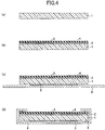
- FIG. 4 is a cross sectional view for explaining the manufacturing method of the RFID tag in the fourth embodiment.
- those parts that are the same as those corresponding parts in FIG. 1 are designated by the same reference numerals, and a description thereof will be omitted.
- a length of the adhesive layer 5 in the horizontal direction is shorter than a length of the metal layer in the horizontal direction.
- a gap 8 is formed by the core 1, the metal layer 6, and the insulator layer 4 at both the end parts of the core 1.
- This gap 8 is formed at the end parts of the core 1, between the lower surface of the core 1 and the metal layer 6, between the side surface of the core 1 and the metal layer 6, and between the upper surface of the insulator layer 4 and the metal layer 6. Both end parts of the adhesive layer 5 are adhered on the upper surface of the insulator layer 4.
- the RFID tag illustrated in (d) of FIG. 4 can be made thin because the thicknesses of the adhesive layers 2 and 5 are slightly reduced during the curing, and the thickness of the RFID tag is 1.745 mm, for example. In addition, the cost and the weight of the RFID tag can also be reduced.
- the metal layer 6 and the dipole antenna formed by the pattern of the metal layer on the insulator layer 4 overlap, to form a loop-shaped antenna.
- the RFID tag is mounted on a metal surface, for example, it is possible to improve the communication distance communicable between the RFID tag and the tag reader (not illustrated) or the tag writer (not illustrated).
- the folded parts of the metal layer 6 hold both ends of the core 1, the insulator layer 4, or the like, and a part of a distortion of the core 1 when the RFID tag is bent is absorbed by the gap 8, even in a case in which the entire RFID tag is bent when mounting the RFID tag on a curved surface, for example, it was confirmed that the insulator layer 4, the metal layer 6, or the like of the RFID tag do not separate from the core 1, and that wrinkles or cracks are uneasily formed in the RFID tag. Moreover, even in a case in which a lower surface of the RFID tag illustrated in (d) of FIG.
- the RFID tag 4 is mounted on a curved surface having a radius of curvature that is 15 mm, for example, using an adhesive tape, it was confirmed that the RFID tag is uneasily broken or damaged. Hence, it was confirmed that the RFID tag is suited for mounting on the curved surface.
- FIG. 5 is a cross sectional view for explaining the manufacturing method of the RFID tag in the fifth embodiment.
- those parts that are the same as those corresponding parts in FIG. 2 are designated by the same reference numerals, and a description thereof will be omitted.
- the length of the adhesive layer 5 in the horizontal direction is shorter than the length of the metal layer in the horizontal direction.
- the gap 8 is formed by the core 1, the metal layer 6, and the insulator layer 4 at both the end parts of the core 1.
- This gap 8 is formed at the end parts of the core 1, between the lower surface of the core 1 and the metal layer 6, between the side surface of the core 1 and the metal layer 6, and between the upper surface of the core 1 and the metal layer 6.
- Both end parts of the adhesive layer 5 are adhered on the upper surface of the insulator layer 4.
- the RFID tag illustrated in (d) of FIG. 5 can be made thin because the thicknesses of the adhesive layers 2 and 5 are slightly reduced during the curing, and the thickness of the RFID tag is 1.745 mm, for example. In addition, the cost and the weight of the RFID tag can also be reduced.
- the metal layer 6 and the dipole antenna formed by the pattern of the metal layer on the insulator layer 4 overlap, to form a loop-shaped antenna.
- the RFID tag is mounted on a metal surface, for example, it is possible to improve the communication distance communicable between the RFID tag and the tag reader (not illustrated) or the tag writer (not illustrated).
- the folded parts of the metal layer 6 hold both ends of the core 1 or the like, and a part of a distortion of the core 1 when the RFID tag is bent is absorbed by the gap 8, even in a case in which the entire RFID tag is bent when mounting the RFID tag on a curved surface, for example, it was confirmed that the insulator layer 4, the metal layer 6, or the like of the RFID tag do not separate from the core 1, and that wrinkles or cracks are uneasily formed in the RFID tag. Moreover, even in a case in which the lower surface of the RFID tag illustrated in (d) of FIG.
- the RFID tag 5 is mounted on a curved surface having a radius of curvature that is 15 mm, for example, using an adhesive tape, it was confirmed that the RFID tag is uneasily broken or damaged. Hence, it was confirmed that the RFID tag is suited for mounting on the curved surface.
- FIG. 6 is a cross sectional view for explaining the manufacturing method of the RFID tag in the sixth embodiment.
- those parts that are the same as those corresponding parts in FIG. 1 are designated by the same reference numerals, and a description thereof will be omitted.
- parts of the RFID tag other than a mounting surface are covered by a protection member, to protect the RFID tag from a temperature environment, a humidity environment, a vibration environment, shock, or the like.
- a box-shaped protection member 21 is prepared, and as illustrated in (b) of FIG. 6 , an adhesive agent 22 is coated on an inner part of the protection member 21.
- the protection member 21 is formed by an elastomer, such as silicone rubber or the like, having a thickness of 0.40 mm, for example.
- the protection member 21 may have a thickness in a range of 0.20 mm to 0.40 mm, for example.
- the adhesive agent 22 is not limited to a particularly adhesive agent as long as the adhesive agent has elasticity after curing, and may be RTV (Room Temperature Vulcanization) silicone rubber or the like, for example.
- the RFID tag in the first embodiment illustrated in (d) of FIG. 1 is turned upside-down, to insert the RFID tag from the side of the insulator layer 4 into an inner side the protection member 21. Accordingly, as illustrated in (d) of FIG. 6 in which the RFID tag is further turned upside-down, the folded parts of the insulator layer 4 and the metal layer 6 of the RFID tag are adhered to the protection member 21 by the adhesive agent 22.
- the lower surface of the protection member 21 and the exposed lower surface of the metal layer 6 of the RFID tag lie approximately on the same plane, and may be mounted on a tag mounting surface, such as a curved surface or the like, using an adhesive tape.
- the thickness of the RFID tag illustrated in (d) of FIG. 6 , including the protection member 21, is 2.145 mm, for example.
- the metal layer 6 and the dipole antenna formed by the pattern of the metal layer on the insulator layer 4 overlap, to form a loop-shaped antenna.
- the RFID tag is mounted on a metal surface, for example, it is possible to improve the communication distance communicable between the RFID tag and the tag reader (not illustrated) or the tag writer (not illustrated).
- the folded parts of the metal layer 6 hold both ends of the core 1, the insulator layer 4, or the like, and the folded parts are held by the protection member 21, even in a case in which the entire RFID tag is bent when mounting the RFID tag on a curved surface, for example, it was confirmed that the insulator layer 4, the metal layer 6, or the like of the RFID tag do not separate from the core 1, and that wrinkles or cracks are uneasily formed in the RFID tag. Moreover, even in a case in which the lower surface of the protection member 21 and the exposed lower surface of the metal layer 6 of the RFID tag illustrated in (d) of FIG.
- the RFID tag 6 are mounted on a curved surface having a radius of curvature that is 15 mm, for example, using an adhesive tape, it was confirmed that the RFID tag is uneasily broken or damaged. Hence, it was confirmed that the RFID tag is suited for mounting on the curved surface. Furthermore, it was confirmed that the RFID tag is protected by the protection member 21 from the temperature environment, the humidity environment, the vibration environment, the shock, or the like.
- the RFID tag illustrated in (d) of FIG. 2 may be inserted from the side of the insulator layer 4 into the inner side of the protection member 21
- the RFID tag illustrated in (d) of FIG. 3 may be inserted from the side of the protection layer 12 into the inner side of the protection member 21
- the RFID tag illustrated in (d) of FIG. 4 may be inserted from the side of the insulator layer 4 into the inner side of the protection member 21
- the RFID tag illustrated in (d) of FIG. 5 may be inserted from the side of the insulator layer 4 into the inner side the protection member 21.
- FIG. 7 is a cross sectional view for explaining the manufacturing method of the RFID tag in the seventh embodiment.
- those parts that are the same as those corresponding parts in FIG. 1 are designated by the same reference numerals, and a description thereof will be omitted.
- the entire surface of the RFID tag is covered by protection members, and a filler material fills a gap between the RFID tag and the protection members, to protect the RFID tag from the temperature environment, the humidity environment, the vibration environment, the shock, or the like.
- a box-shaped protection member 31 is prepared, and as illustrated in (b) of FIG. 7 , an adhesive agent 32 is coated on an inner part of the protection member 31.
- the protection member 31 is formed by an elastomer, such as silicone rubber or the like, having a thickness of 0.40 mm, for example.
- the protection member 31 may have a thickness in a range of 0.20 mm to 0.40 mm, for example.
- the adhesive agent 32 is not limited to a particularly adhesive agent as long as the adhesive agent has elasticity after curing, and may be RTV silicone rubber or the like, for example.
- the RFID tag in the first embodiment illustrated in (d) of FIG. 1 is inserted from the side of the metal layer 6 into an inner side the protection member 31. Accordingly, as illustrated in (c) of FIG. 7 , the metal layer 6 of the RFID tag is adhered on the protection member 31 by the adhesive agent 32.
- an adhesive agent 33 is coated on the upper surface of the RFID tag, and a box-shaped protection member 34 is adhered on the RFID tag and the protection member 31 via the adhesive agent 33.
- the protection member 34 may be made of the same material as the protection member 31, and have the same thickness as the protection member 31.
- the adhesive agent 33 may be made of the same material as the adhesive agent 32.
- the protection members 31 and 34 that are mutually adhered form a package or a casing that protects the RFID tag.
- An adhesive agent 35 at the parts connecting the protection members 31 and 34 may be any of the adhesive agent 32, the adhesive agent 33, a mixture of the adhesive agents 32 and 33, and an adhesive agent other than the adhesive agents 32 and 33. Accordingly, as illustrated in (d) of FIG. 7 , the RFID tag is encapsulated by the protection members 31 and 34, and a space between the RFID tag and the protection members 31 and 34 is filled by the adhesive agents 32 and 33 that also function as a filler material.
- the adhesive agents 32 and 33 that function as the filler material can suppress a change in shape of the RFID tag encapsulated within the protection members 31 and 34, particularly due to a change in pressure.
- the RFID tag may be mounted on the tag mounting surface, such as a curved surface or the like, by mounting a lower surface of the protection member 31 on the tag mounting surface using an adhesive tape.
- the thickness of the RFID tag, including the protection members 31 and 34 illustrated in (d) of FIG. 7 is 2.590 mm, for example.
- the metal layer 6 and the dipole antenna formed by the pattern of the metal layer on the insulator layer 4 overlap, to form a loop-shaped antenna.
- the RFID tag is mounted on a metal surface, for example, it is possible to improve the communication distance communicable between the RFID tag and the tag reader (not illustrated) or the tag writer (not illustrated).
- the folded parts of the metal layer 6 hold both ends of the core 1, the insulator layer 4, or the like, and the folded parts are held by the protection members 31 and 34, even in a case in which the entire RFID tag is bent when mounting the RFID tag on a curved surface, for example, it was confirmed that the insulator layer 4, the metal layer 6, or the like of the RFID tag do not separate from the core 1, and that wrinkles or cracks are uneasily formed in the RFID tag. Moreover, even in a case in which the lower surface of the protection member 21 of the RFID tag illustrated in (d) of FIG.
- the RFID tag 7 is mounted on a curved surface having a radius of curvature that is 15 mm, for example, using an adhesive tape, it was confirmed that the RFID tag is uneasily broken or damaged. Hence, it was confirmed that the RFID tag is suited for mounting on the curved surface. Furthermore, it was confirmed that the RFID tag is protected by the protection members 31 and 34 from the temperature environment, the humidity environment, the vibration environment, the shock, or the like.
- the RFID tag illustrated in (d) of FIG. 2 may be inserted from the side of the metal layer 6 into the inner side of the protection member 31, and the RFID tag illustrated in (d) of FIG. 3 may be inserted from the side of the metal layer 6 into the inner side of the protection member 31.
- the RFID tag illustrated in (d) of FIG. 1 may be inserted from the side of the insulator layer 4 into the inner side of the protection member 31.
- the RFID tag illustrated in (d) of FIG. 2 may be inserted from the side of the insulator layer 4 into the inner side of the protection member 31, and the RFID tag illustrated in (d) of FIG. 3 may be inserted from the side of the protection layer 12 into the inner side of the protection member 31.
- the RFID tag may first be inserted into the protection member 34, and the protection member 31 may thereafter be connected to the protection member 34.
- the RFID tag illustrated in (d) of FIG. 1 the RFID tag illustrated in (d) of FIG. 2 or illustrated in (d) of FIG. 3 may be inserted in a similar manner.
- depths of the inner parts of the protection members 31 and 34 are approximately the same in the example illustrated in FIG. 7 , the depth of one of the protection members 31 and 34 may of course be deeper than the other.
- FIG. 8 is a cross sectional view for explaining the manufacturing method of the RFID tag in the eighth embodiment.
- those parts that are the same as those corresponding parts in FIG. 7 are designated by the same reference numerals, and a description thereof will be omitted.
- the entire surface of the RFID tag is covered by protection members, and a gap is maintained between the RFID tag and the protection members, to protect the RFID tag from the temperature environment, the humidity environment, the vibration environment, the shock, or the like.
- the box-shaped protection member 31 is prepared.
- the RFID tag in the fourth embodiment illustrated in (d) of FIG. 4 is inserted from the side of the metal layer 6 into the inner part of the protection member 31, as illustrated in (c) of FIG. 8 .
- the RFID tag and the protection member 31 are covered by the box-shaped protection member 34, and the protection members 31 and 34 are adhered by the adhesive agent 35.
- the RFID tag is encapsulated by the protection members 31 and 34, and the space between the RFID tag and the protection members 31 and 34 is maintained.
- the RFID tag may be mounted on the tag mounting surface, such as a curved surface or the like, by mounting the lower surface of the protection member 31 using an adhesive tape.
- the thickness of the RFID tag, including the protection members 31 and 34 illustrated in (d) of FIG. 8 is 2.590 mm, for example.
- the metal layer 6 and the dipole antenna formed by the pattern of the metal layer on the insulator layer 4 overlap, to form a loop-shaped antenna.
- the RFID tag is mounted on a metal surface, for example, it is possible to improve the communication distance communicable between the RFID tag and the tag reader (not illustrated) or the tag writer (not illustrated).
- the folded parts of the metal layer 6 hold both ends of the core 1, the insulator layer 4, or the like, and a part of the distortion of the core 1 when the RFID tag is bent is absorbed by the gap 8 and the gap between the RFID tag and the protection members 31 and 34, even in a case in which the entire RFID tag is bent when mounting the RFID tag on a curved surface, for example, it was confirmed that the insulator layer 4, the metal layer 6, or the like of the RFID tag do not separate from the core 1, and that wrinkles or cracks are uneasily formed in the RFID tag.
- the insulator layer 4, the metal layer 6, or the like of the RFID tag do not separate from the core 1, and that wrinkles or cracks are uneasily formed in the RFID tag.
- the lower surface of the protection member 31 of the RFID tag illustrated in (d) of FIG. 8 is mounted on a curved surface having a radius of curvature that is 15 mm, for example, using an adhesive tape, it was confirmed that the RFID tag is uneasily broken or damaged. Hence, it was confirmed that the RFID tag is suited for mounting on the curved surface.
- the RFID tag is protected by the protection members 31 and 34 from the temperature environment, the humidity environment, the vibration environment, the shock, or the like.
- this embodiment it is possible to reduce the weight of the RFID tag including the protection members 31 and 34 when compared to the seventh embodiment described above, because this embodiment does not use a filler material to fill the gap.
- the RFID tag illustrated in (d) of FIG. 5 may be inserted from the side of the metal layer 6 into the inner side of the protection member 31.
- the RFID tag illustrated in (d) of FIG. 4 may be inserted from the side of the insulator layer 4 into the inner side of the protection member 31.
- the RFID tag illustrated in (d) of FIG. 5 may be inserted from the side of the insulator layer 4 into the inner side of the protection member 31.
- the RFID tag may first be inserted into the protection member 34, and the protection member 31 may thereafter be connected to the protection member 34.
- the RFID tag illustrated in (d) of FIG. 4 may be inserted in a similar manner.
- the depth of one of the protection members 31 and 34 may of course be deeper than the other.
- the adhesive agent 35 may be intermittently coated, to form an opening communicating a space surrounded by the protection members 31 and 34 to an outside of the protection members 31 and 34.
- FIG. 9 is a plan view, partially in a perspective, of the RFID tag in the eighth embodiment.
- FIG. 9 illustrates the RFID tag in a state in which the protection members 31 and 34 are removed.
- a pattern 41 of a metal layer is formed on a surface (lower side of paper in FIG. 9 ) of the insulator layer 4 on the side of the core 1.
- the shape of the pattern 41 of the metal layer is not limited to a particular shape as long as the pattern 41 is able to form a dipole antenna. Terminals of the tag chip 3 that is indicated by a solid line for the sake of convenience to facilitate visual confirmation are electrically connected to the pattern 41 of the metal layer.
- the metal layer 6 and a part of the pattern 41 of the metal layer on the insulator layer 4 overlap at the folded parts of the metal layer 6.
- the pattern of the metal layer formed on the insulator layer 4 in the first through eighth embodiments described above may be similar to the pattern 41 of the metal layer illustrated in FIG. 9 .
- FIG. 10 is a cross sectional view for explaining the manufacturing method of the RFID tag in a ninth embodiment.
- those parts that are the same as those corresponding parts in FIG. 1 are designated by the same reference numerals, and a description thereof will be omitted.
- the insulator layer 4 is folded at both end parts of the core 1.
- the insulator layer 4 is once bent in a vertical direction (downward direction) along the end parts of the core 1, and is further bent in a horizontal direction (that is, in a direction towards the central part of the core 1) along the lower surface of the metal layer 6.
- the insulator layer 4 is folded in a horizontal U-shape at both end parts of the core 1.
- the adhesive layer 2 and the insulator layer 4 may have approximately the same sizes, so that the insulator layer 4 is adhered to the side surface of the core 1 and the lower surface of the metal layer 6 via the adhesive layer 2.
- the RFID tag illustrated in FIG. 10 can be made thin because the thicknesses of the adhesive layers 2 and 5 are slightly reduced during the curing, and the thickness of the RFID tag is 1.505 mm, for example. In addition, the cost and the weight of the RFID tag can also be reduced.
- the metal layer 6 and the dipole antenna formed by the pattern of the metal layer on the insulator layer 4 overlap, to form a loop-shaped antenna.
- the insulator layer 4 holds both ends of the core 1 or the like, and a part of a distortion of the core 1 when the RFID tag is bent is absorbed by the gap 8, even in a case in which the entire RFID tag is bent when mounting the RFID tag on a curved surface, for example, it was confirmed that the insulator layer 4, the metal layer 6, or the like of the RFID tag do not separate from the core 1, and that wrinkles or cracks are uneasily formed in the RFID tag.
- the RFID tag illustrated in FIG. 10 is mounted on a curved surface having a radius of curvature that is 15 mm, for example, using an adhesive tape, it was confirmed that the RFID tag is uneasily broken or damaged. Hence, it was confirmed that the RFID tag is suited for mounting on the curved surface.
- the protection layer 12 may be formed on the lower surface of the RFID tag illustrated in FIG. 10 via the adhesive layer 11 similar to that of FIG. 3 .
- FIG. 11 is a cross sectional view for explaining the manufacturing method of the RFID tag in a tenth embodiment.
- those parts that are the same as those corresponding parts in FIGs. 6 and 10 are designated by the same reference numerals, and a description thereof will be omitted.
- an RFID tag having a configuration similar to that of FIG. 10 has the protection member 21 adhered thereon by the adhesive agent 22.
- an adhesive layer 37 is adhered on the folded parts of the insulator layer 4 and the exposed lower surface of the metal layer 6.
- the thickness of the RFID tag including the protection member 21 illustrated in FIG. 11 is 1.895 mm, for example.
- the metal layer 6 and the dipole antenna formed by the pattern of the metal layer on the insulator layer 4 overlap, to form a loop-shaped antenna.
- the folded parts of the insulator layer 4 hold both ends of the core 1, the insulator layer 4, or the like, and the folded parts are held by the protection member 21, even in a case in which the entire RFID tag is bent when mounting the RFID tag on a curved surface, for example, it was confirmed that the insulator layer 4, the metal layer 6, or the like of the RFID tag do not separate from the core 1, and that wrinkles or cracks are uneasily formed in the RFID tag.
- the RFID tag 11 are mounted on a curved surface having a radius of curvature that is 15 mm, for example, using an adhesive tape, it was confirmed that the RFID tag is uneasily broken or damaged. Hence, it was confirmed that the RFID tag is suited for mounting on the curved surface. Furthermore, it was confirmed that the RFID tag is protected by the protection member 21 from the temperature environment, the humidity environment, the vibration environment, the shock, or the like.
- FIG. 12 is a cross sectional view for explaining the manufacturing method of the RFID tag in an eleventh embodiment.
- those parts that are the same as those corresponding parts in FIG. 1 are designated by the same reference numerals, and a description thereof will be omitted.
- the insulator layer 4 is folded at both end parts of the core 1.
- the insulator layer 4 is once bent in a vertical direction (downward direction) along the end parts of the core 1, and is further bent in a horizontal direction (that is, in a direction towards the central part of the core 1) along the lower surface of the core 1.
- the insulator layer 4 is folded in a horizontal U-shape at both end parts of the core 1.
- the adhesive layer 2 and the insulator layer 4 may have approximately the same sizes, so that the insulator layer 4 is adhered to the side surface of the core 1 and a part of the lower surface of the core 1 via the adhesive layer 2.
- the metal layer 6 is adhered on the folded parts of the insulator layer 4 and the exposed lower surface of the core 1 via the adhesive layer 5.
- the adhesive layer 5 may also be provided between the metal layer 6 and the folded parts of the insulator layer 4.
- the RFID tag illustrated in FIG. 12 can be made thin because the thicknesses of the adhesive layers 2 and 5 are slightly reduced during the curing, and the thickness of the RFID tag is 1.505 mm, for example. In addition, the cost and the weight of the RFID tag can also be reduced.
- the metal layer 6 and the dipole antenna formed by the pattern of the metal layer on the insulator layer 4 overlap, to form a loop-shaped antenna.
- the folded parts of the insulator layer 4 are held by the metal layer 6, even in a case in which the entire RFID tag is bent when mounting the RFID tag on a curved surface, for example, it was confirmed that the insulator layer 4, the metal layer 6, or the like of the RFID tag do not separate from the core 1, and that wrinkles or cracks are uneasily formed in the RFID tag.
- the lower surface of the RFID tag illustrated in FIG. 12 is mounted on a curved surface having a radius of curvature that is 15 mm, for example, using an adhesive tape, it was confirmed that the RFID tag is uneasily broken or damaged. Hence, it was confirmed that the RFID tag is suited for mounting on the curved surface.
- the RFID tag illustrated in FIG. 12 may be inserted into the protection member 21 illustrated in FIG. 11 .
- FIG. 13 is a cross sectional view for explaining the manufacturing method of the RFID tag in a twelfth embodiment.
- those parts that are the same as those corresponding parts in FIGs. 7 and 10 are designated by the same reference numerals, and a description thereof will be omitted.
- an RFID tag having a configuration similar to that of FIG. 10 is encapsulated by the protection members 31 and 34, and the gap between the RFID tag and the protection members 31 and 34 is filled by the adhesive agents 32 and 33 that also function as the filler material.
- the adhesive agents 32 and 33 that function as the filler material can suppress a change in shape of the RFID tag encapsulated within the protection members 31 and 34, particularly due to a change in pressure.
- the thickness of the RFID tag, including the protection members 31 and 34 illustrated in FIG. 13 is 2.35 mm, for example.
- the metal layer 6 and the dipole antenna formed by the pattern of the metal layer on the insulator layer 4 overlap, to form a loop-shaped antenna.
- the insulator layer 4 holds both ends of the core 1, the metal layer 6, or the like, and the folded parts are held by the protection members 31 and 34, even in a case in which the entire RFID tag is bent when mounting the RFID tag on a curved surface, for example, it was confirmed that the insulator layer 4, the metal layer 6, or the like of the RFID tag do not separate from the core 1, and that wrinkles or cracks are uneasily formed in the RFID tag.
- the lower surface of the protection member 21 of the RFID tag illustrated in FIG. 13 is mounted on a curved surface having a radius of curvature that is 15 mm, for example, using an adhesive tape, it was confirmed that the RFID tag is uneasily broken or damaged.
- the RFID tag is suited for mounting on the curved surface.
- the RFID tag is protected by the protection members 31 and 34 from the temperature environment, the humidity environment, the vibration environment, the shock, or the like.
- the RFID tag illustrated in FIG. 12 may be inserted from the side of the metal layer 6 into the inner side of the protection member 31.
- the RFID tag illustrated in FIG. 12 may be inserted from the side of the insulator layer 4 into the inner side of the protection member 31.
- the RFID tag may first be inserted into the protection member 34, and the protection member 31 may thereafter be connected to the protection member 34.
- the RFID tag illustrated in FIG. 12 may be inserted in a similar manner.
- depths of the inner parts of the protection members 31 and 34 are approximately the same in the example illustrated in FIG. 13 , the depth of one of the protection members 31 and 34 may of course be deeper than the other.
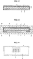
- FIG. 14 is a plan view, partially in a perspective, of the RFID tag in the twelfth embodiment.
- FIG. 14 illustrates the RFID tag in a state in which the protection members 31 and 34 are removed.
- the pattern 41 of the metal layer is formed on the surface (lower side of paper in FIG. 14 ) of the insulator layer 4 on the side of the core 1.
- the shape of the pattern 41 of the metal layer is not limited to a particular shape as long as the pattern 41 is able to form a dipole antenna. Terminals of the tag chip 3 that is indicated by a solid line for the sake of convenience to facilitate visual confirmation are electrically connected to the pattern 41 of the metal layer.
- the pattern of the metal layer formed on the insulator layer 4 in the ninth through eleventh embodiments described above may be similar to the pattern 41 of the metal layer illustrated in FIG. 14 .
- the thickness of the RFID tag using no protection member 21 or no protection members 31 and 34 can be reduced to approximately 1.0 mm.
- the RFID tag using no protection member 21 or no protection members 31 and 34 may be used in an interior environment (environment in which the temperature, the pressure, or the like are adjusted, as in the case of a cabin of an aircraft) of RTCA/DO-160, SAE/AS5678, or the like, for example, which are standards for the RFID tag.
- the thickness of the RFID tag using the protection member 21 or the protection members 31 and 34 can be reduced to approximately 2.0 mm.
- the RFID tag using the protection member 21 or the protection members 31 and 34 may be used in an exterior environment (environment in which the temperature, the pressure, or the like are not adjusted, as in the case of a landing gear well of the aircraft) of RTCA/DO-160, SAE/AS5678, or the like, for example, which are standards for the RFID tag, and a power plant environment (high-temperature environment, such as a periphery of an engine of the aircraft).
- an exterior environment environment in which the temperature, the pressure, or the like are not adjusted, as in the case of a landing gear well of the aircraft
- RTCA/DO-160, SAE/AS5678, or the like for example, which are standards for the RFID tag
- a power plant environment high-temperature environment, such as a periphery of an engine of the aircraft.
- FIG. 15 is a block diagram illustrating an example of a hardware configuration of the passive type RFID tag.
- the passive type RFID tag illustrated in FIG. 15 includes a loop-shaped antenna 51 which is an example of the dipole antenna, and a tag chip 52-1 which is an example of the semiconductor chip.
- the tag chip 52-1 include a power generating part 53 which is an example of a power supply, a transmitting and receiving part 54 which is an example of a communication part, a data processing part 55, and a memory 56 which is an example of a storage part.
- the power generating part 53 generates, by a known method, a power supply voltage from radio waves received via the antenna 51, and supplies the power supply voltage to each part within the tag chip 52-1.
- the transmitting and receiving part 54 may include a demodulator part that demodulates received data according to a modulation technique corresponding to a modulation technique of the tag writer (not illustrated), and a modulator that modules transmitting data according to a modulation technique corresponding to a modulation technique of the tag reader (not illustrated).
- the data processing part 55 performs a decoding process to subject the demodulated received data to a decoding corresponding to a coding technique of the tag writer, a coding process to subject the transmitting data to be modulated to a coding corresponding to a coding technique of the tag reader, a control process to control read and write of the data with respect to the memory 56, or the like.
- the data processing part 55 may include a codec that performs the decoding process and the coding process, and a controller that performs the control process.
- the data processing part 55 may include a processor, such as a CPU (Central Processing Unit), that performs the decoding process, the coding process, and the control process.
- the tag chip 52-1 is mounted at a central part of the surface of the core 1 provided with the metal layer or the dipole antenna, for example, using an adhesive agent or the like.
- the tag chip 52-1 may include one or a plurality of sensors 57.
- data related to information such as the temperature, the humidity, the pressure, or the like detected by the sensor 57 may be stored in the memory 56 together with time information such as the time, the date and time, or the like managed by the data processing part 55.
- FIG. 16 is a block diagram illustrating an example of a hardware configuration of the active type RFID tag.
- the active type RFID tag illustrated in FIG. 16 includes the loop-shaped antenna 51, a tag chip 52-2, and a battery 531 which is an example of a power supply.
- the battery 531 supplies a power supply voltage to each part within the tag chip 52-2.
- the type of the battery 531 is not limited to a particular type, and the number of batteries 531 is not limited to a particular number.
- the tag chip 52-2 and the battery 531 are mounted at the central part of the surface of the core 1 provided with the metal layer or the dipole antenna, for example, using an adhesive agent or the like.
- the RFID tag illustrated in FIG. 16 includes functions of the active type RFID tag, however, this RFID tag may form a semi-active type RFID tag that starts communication with a host system, for example, by a system similar to that of the passive type RFID tag.
- the active type RFID tag and the semi-active type RFID tag is provided with the battery 531 in place of the power generating part 53, and differ from the passive type RFID tag in that this battery 531 is connected to the the chip 52-2.
- the configuration of other parts of the active type RFID tag and the semi-active type RFID tag may be similar to that of the passive type RFID tag. Accordingly, in the first through twelfth embodiments described above in conjunction with FIGs. 1 through 14 , the RFID tag may of course form the active type RFID tag or the semi-active type RFID tag by providing the battery 531 in place of the power generating part 53 and connecting this battery 531 to the tag chip 52-1 which corresponds to the tag chip 3.
- the disclosed RFID tag is particularly suited for mounting on the curved surface, however, the surface on which the RFID tag is mounted is not limited to the curved surface, and the RFID tag may of course be mounted on a flat surface.
- the shape of the RFID tag in the plan view is not limited to the rectangular shape, and the shape of the RFID tag may be selected arbitrarily according to the usage of the RFID tag.
- the RFID tag may be provided integrally On a rewritable RFID sheet, for example.
- the RFID tag may be printed by a known RFID tag so that data related to log information, management information, or the like of the components, for example, are written into the memory of the RFID tag in a manner readable by the RFID tag reader, and character data related to the log information, the management information, or the like of the components are printed on the rewritable RFID sheet in a manner visible by a user.
- the metal layer and the dipole antenna overlap at the folded parts where one of the metal layer and the dipole antenna is folded at a pair of end parts, however, the overlapping parts of the metal layer and the dipole antenna may be adhered by an adhesive agent.
- the adhesive agent adhering the overlapping parts of the metal layer and the dipole antenna may be conductive or non-conductive.
Landscapes
- Engineering & Computer Science (AREA)
- Physics & Mathematics (AREA)
- General Physics & Mathematics (AREA)
- Theoretical Computer Science (AREA)
- Computer Networks & Wireless Communication (AREA)
- Computer Hardware Design (AREA)
- Microelectronics & Electronic Packaging (AREA)
- Details Of Aerials (AREA)
Abstract
Description
- The present invention relates to an RFID (Radio Frequency IDentification) tag and a manufacturing method thereof. The RFID tag is sometimes also referred to as an IC (Integrated Circuit) tag.
- The RFID tag is used in various fields. In addition, a communication system between the RFID tag and a tag reader or a tag writer includes an electromagnetic induction system and a radio wave system. The RFID tag may be mounted on a curved surface, a metal surface, or the like. In a case in which the RFID tag is mounted on the curved surface, a core of the RFID is desirably formed by an elastic material.
- On the other hand, in a case in which the radio wave system RFID is mounted on the metal surface, a communication distance communicable between the RFID tag and the tag reader or the tag writer can be improved by forming an antenna in a loop shape. However, in a case in which when mounting the RFID tag on an inner side or an outer side of a metal pipe having a relatively small diameter, for example, it is difficult to form the loop-shaped antenna part to have a suitable elasticity, even when the core of the RFID tag is formed by the elastic material. For this reason, as a radius of curvature of the curved surface becomes smaller, wrinkles or cracks may be formed at the loop-shaped antenna part of the RFID tag, and in a worst case, the RFID tag is broken or damaged. In addition, in a case in which the RFID tag is adhered on the curved surface using an adhesive tape or the like, the smaller the radius or curvature of the curves surface, the easier the mounted RFID tag separates from the adhered curved surface, because it is difficult to form the loop-shaped antenna part to have the suitable elasticity.
- The curved surface may include a plurality of concave parts and convex parts, or a plurality of concave parts or convex parts having different radii of curvature. In these cases, it is also difficult to mount the RFID tag having the loop-shaped antenna on the curved surface.
-
- Patent Document 1: Japanese Laid-Open Patent Publication No.
2006-53833 - Patent Document 2: Japanese Laid-Open Patent Publication No.
2011-109552 - Patent Document 3: Japanese Laid-Open Patent Publication No.
2008-90813 - There is a problem in that the conventional RFID tag having the loop-shaped antenna is unsuited for mounting on the curved surface.
- One object of the present invention is to provide an RFID tag having a loop-shaped antenna and suited for mounted on a curved surface, and a manufacturing method thereof.
- According to one aspect of the present invention, an RFID tag includes a core formed by a first elastic material and having a first surface, a second surface on an opposite side of the first surface, and a pair of end parts provided on mutually opposite sides and connecting to the first surface and the second surface; a first metal layer provided on the first surface; a semiconductor chip provided on the second surface and having a communication part; and a dipole antenna provided on the second surface and electrically connected to the semiconductor chip, wherein one of the first metal layer and the dipole antenna is folded at folded parts at the pair of end parts, and the first metal layer and the dipole antenna overlap at the folded parts.
- According to the disclosed RFID tag and manufacturing method thereof, it is possible to provide an RFID tag having a loop-shaped antenna and suited for mounting on a curved surface.
-
-
FIG. 1 is a cross sectional view for explaining a manufacturing method of an RFID tag in a first embodiment; -
FIG. 2 is a cross sectional view for explaining the manufacturing method of the RFID tag in a second embodiment; -
FIG. 3 is a cross sectional view for explaining the manufacturing method of the RFID tag in a third embodiment; -
FIG. 4 is a cross sectional view for explaining the manufacturing method of the RFID tag in a fourth embodiment; -
FIG. 5 is a cross sectional view for explaining the manufacturing method of the RFID tag in a fifth embodiment; -
FIG. 6 is a cross sectional view for explaining the manufacturing method of the RFID tag in a sixth embodiment; -
FIG. 7 is a cross sectional view for explaining the manufacturing method of the RFID tag in a seventh embodiment; -
FIG. 8 is a cross sectional view for explaining the manufacturing method of the RFID tag in an eighth embodiment; -
FIG. 9 is a plan view, partially in a perspective, of the RFID tag in the eighth embodiment; -
FIG. 10 is a cross sectional view for explaining the manufacturing method of the RFID tag in a ninth embodiment; -
FIG. 11 is a cross sectional view for explaining the manufacturing method of the RFID tag in a tenth embodiment; -
FIG. 12 is a cross sectional view for explaining the manufacturing method of the RFID tag in an eleventh embodiment; -
FIG. 13 is a cross sectional view for explaining the manufacturing method of the RFID tag in a twelfth embodiment; -
FIG. 14 is a plan view, partially in a perspective, of the RFID tag in the twelfth embodiment; -
FIG. 15 is a block diagram illustrating an example of a hardware configuration of a passive type RFID tag; and -
FIG. 16 is a block diagram illustrating an example of a hardware configuration of an active type RFID tag. - According to the disclosed RFID tag and manufacturing method thereof, a core is formed by an elastic material and has a first surface, a second surface on an opposite side of the first surface, and a pair of end parts provided on mutually opposite sides and connecting to the first surface and the second surface. A first metal layer is provided on the first surface, and a semiconductor chip provided on the second surface and has a communication part. A dipole antenna is provided on the second surface and is electrically connected to the semiconductor chip. One of the first metal layer and the dipole antenna is folded at folded parts at the pair of end parts, and the first metal layer and the dipole antenna overlap at the folded parts.
- Next, a description will be given the disclosed RFID tag and manufacturing method thereof in each embodiment, by referring to the drawings.
- First, a description will be given of a manufacturing method of an RFID tag in a first embodiment, by referring to
FIG. 1. FIG. 1 is a cross sectional view for explaining the manufacturing method of the RFID tag in the first embodiment. InFIG. 1 andFIGs. 2 through 14 which will be described later, dimensions including thicknesses of each of layers are illustrated for easy viewing, and proportions of the dimensions including the thicknesses of each of the layers in these figures do not correspond to actual proportions of the dimensions including the thicknesses of each of the layers. - First, as illustrated in (a) of
FIG. 1 , acore 1 formed by an elastic material is prepared. In this example, thecore 1 is formed by a plate-shaped dielectric having a thickness of 0.8 mm, for example, and has a rectangular shape in a plan view. The dielectric may be PVC (Poly-Vinyl Chloride), silicone rubber, or the like, for example. Thecore 1 has a flat lower surface which is an example of a first surface, and a flat upper surface which is an example of a second surface. The thickness of the dielectric forming thecore 1 may be in a range of 0.5 mm to 1.5 mm, for example. - Next, as illustrated in (b) of
FIG. 1 , anadhesive layer 2 having a thickness of 0.05 mm, for example, is formed on the upper surface of thecore 1. An adhesive agent used for theadhesive layer 2 is not limited to a particular adhesive agent as long as the adhesive agent has elasticity after curing. The thickness of theadhesive layer 2 may be in a range of 0.05 mm to 0.15 mm, for example. Atag chip 3 which is an example of a semiconductor chip, is provided on a surface of aninsulator layer 4 formed by an elastic material and formed with a pattern of a metal layer (not illustrated). The surface (lower surface in (b) ofFIG. 1 ) of theinsulator layer 4 provided with the pattern of the metal layer and thetag chip 3 is adhered on theadhesive layer 2. The pattern of the metal layer made of copper (Cu), silver (Ag), gold (Au), aluminum (Al), or the like is formed on one surface of a PET (Poly-Ethylene Terephthalate) having a thickness of 0.05 mm, for example, and a part of thetag chip 3 electrically connecting to the patterns of the metal layer has a thickness of 0.21 mm, for example. The pattern of the metal layer forms a dipole antenna. In this example, thetag chip 3 is provided at a central part of the surface of theinsulator layer 4 formed with the pattern of the metal layer, and thus, in a state in which theinsulator layer 4 is adhered to theadhesive layer 2, thetag chip 3 is provided at a central part of the upper surface of thecore 1. - Next, as illustrated in (c) of
FIG. 1 , anadhesive layer 5 having a thickness of 0.05 mm, for example, is formed on the lower surface of thecore 1. An adhesive agent used for theadhesive layer 5 is not limited to a particular adhesive agent as long as the adhesive agent has elasticity after curing, and may be the same as the adhesive agent used for theadhesive layer 2. The thickness of theadhesive layer 5 may be in a range of 0.05 mm to 0.15 mm, for example. Ametal layer 6 is adhered to theadhesive layer 5. Themetal layer 6 is formed by a metal or alloy that is relatively soft and suited for bending, such as tin (Sn), zinc (Zn), lead (Pb), indium (In), or an alloy including at least one of these metals, and has a thickness of 0.30 mm, for example. In this example, the metal forming the pattern of the metal layer formed on theinsulator layer 4 and the metal forming themetal layer 6 are different. The thickness of themetal layer 6 may be in a range of 0.15 mm to 0.30 mm, for example. - Next, as illustrated in (d) of
FIG. 1 , theadhesive layer 5 and themetal layer 6 are folded at both end parts of thecore 1. In the example illustrated in (d) ofFIG. 1 , theadhesive layer 5 and themetal layer 6 are once bent in a vertical direction (upward direction) along the end parts of thecore 1, and are further bent in a horizontal direction (that is, in a direction towards the central part provided with the tag chip 3) along an upper surface of theinsulator layer 4. In other words, theadhesive layer 5 and themetal layer 6 are folded in a horizontal U-shape at both end parts of thecore 1. Accordingly, both end parts of theadhesive layer 5 are adhered on the upper surface of theinsulator layer 4. The RFID tag illustrated in (d) ofFIG. 1 can be made thin because the thicknesses of theadhesive layers - At the folded parts where the
metal layer 6 is folded in the horizontal U-shape at both end parts of thecore 1, themetal layer 6 and the dipole antenna formed by the pattern of the metal layer on theinsulator layer 4 overlap, to form a loop-shaped antenna. Hence, even in a case in which the RFID tag is mounted on a metal surface, for example, it is possible to improve a communication distance communicable between the RFID tag and a tag reader (not illustrated) or a tag writer (not illustrated). - In addition, because the folded parts of the
metal layer 6 hold both ends of theinsulator layer 4 or the like, even in a case in which the entire RFID tag is bent when mounting the RFID tag on a curved surface, for example, it was confirmed that theinsulator layer 4, themetal layer 6, or the like of the RFID tag do not separate from thecore 1, and that wrinkles or cracks are uneasily formed in the RFID tag. Moreover, even in a case in which a lower surface of the RFID tag illustrated in (d) ofFIG. 1 is mounted on a curved surface having a radius of curvature that is 15 mm, for example, using an adhesive tape, it was confirmed that the RFID tag is uneasily broken or damaged. Hence, it was confirmed that the RFID tag is suited for mounting on the curved surface. - Next, a description will be given of the manufacturing method of the RFID tag in a second embodiment, by referring to
FIG. 2. FIG. 2 is a cross sectional view for explaining the manufacturing method of the RFID tag in the second embodiment. InFIG. 2 , those parts that are the same as those corresponding parts inFIG. 1 are designated by the same reference numerals, and a description thereof will be omitted. - First, as illustrated in (a) of
FIG. 2 , thecore 1 formed by an elastic material is prepared. - Next, as illustrated in (b) of
FIG. 2 , theadhesive layer 5 is formed on the lower surface of thecore 1. Themetal layer 6 is adhered on theadhesive layer 5. - Next, as illustrated in (c) of
FIG. 2 , theadhesive layer 5 and themetal layer 6 are folded at both end parts of thecore 1. In the example illustrated in (c) ofFIG. 2 , theadhesive layer 5 and themetal layer 6 are once bent in a vertical direction (upward direction) along the end parts of thecore 1, and are further bent in a horizontal direction (that is, in a direction towards a central part provided with the tag chip 3) along the upper surface of thecore 1. In other words, theadhesive layer 5 and themetal layer 6 are folded in a horizontal U-shape at both end parts of thecore 1. Accordingly, both end parts of theadhesive layer 5 are adhered on the upper surface of thecore 1. - Next, as illustrated in (d) of
FIG. 2 , theadhesive layer 2 is formed on the upper surface of thecore 1, and on an upper surface of folded parts where themetal layer 6 is folded in the horizontal U-shape at both end parts of thecore 1. Thetag chip 3 is provided on the surface of theinsulator layer 4 formed by an elastic material, and formed with the pattern of the metal layer (not illustrated). The surface (lower surface in (d) ofFIG. 2 ) of theinsulator layer 4 provided with the pattern of the metal layer and thetag chip 3 is adhered on theadhesive layer 2, and formed with the pattern of the metal layer (not illustrated). The RFID tag illustrated in (d) ofFIG. 2 can be made thin because the thicknesses of theadhesive layers insulator layer 4 is formed on the folded parts of themetal layer 6, not only the lower surface but also the upper surface of the RFID tag can be made flat. - At the folded parts where the
metal layer 6 is folded in the horizontal U-shape at both end parts of thecore 1, themetal layer 6 and the dipole antenna formed by the pattern of the metal layer on theinsulator layer 4 overlap, to form a loop-shaped antenna. Hence, even in a case in which the RFID tag is mounted on a metal surface, for example, it is possible to improve the communication distance communicable between the RFID tag and the tag reader (not illustrated) or the tag writer (not illustrated). - In addition, because the folded parts of the
metal layer 6 hold both ends of thecore 1, theinsulator layer 4, or the like, even in a case in which the entire RFID tag is bent when mounting the RFID tag on a curved surface, for example, it was confirmed that theinsulator layer 4, themetal layer 6, or the like of the RFID tag do not separate from thecore 1, and that wrinkles or cracks are uneasily formed in the RFID tag. Moreover, even in a case in which a lower surface or an upper surface of the RFID tag illustrated in (d) ofFIG. 2 is mounted on a curved surface having a radius of curvature that is 15 mm, for example, using an adhesive tape, it was confirmed that the RFID tag is uneasily broken or damaged. Hence, it was confirmed that the RFID tag is suited for mounting on the curved surface. - Next, a description will be given of the manufacturing method of the RFID tag in a third embodiment, by referring to
FIG. 3. FIG. 3 is a cross sectional view for explaining the manufacturing method of the RFID tag in the third embodiment. InFIG. 3 , those parts that are the same as those corresponding parts inFIG. 1 are designated by the same reference numerals, and a description thereof will be omitted. In this embodiment, a protection layer is formed on the upper surfaces of theinsulator layer 4 and the folded parts in (d) ofFIG. 1 . - As illustrated in (a) and (b) of
FIG. 3 , aprotection layer 12 is formed on the upper surface of the RFID tag in the first embodiment illustrated in (d) ofFIG. 1 , via anadhesive layer 11. An adhesive agent used for theadhesive layer 11 is not limited to a particular adhesive agent as long as the adhesive agent has elasticity after curing, and may be the same as the adhesive agent used for theadhesive layer 2 or theadhesive layer 5. A material used for theprotection layer 12 is not limited to a particular material as long as the material has elasticity, and may be a flame resistant material, for example. Theadhesive layer 11 has a thickness of 0.05 mm, for example, and theprotection layer 12 has a thickness of 0.15 mm, for example. A combination of theadhesive layer 11 and theprotection layer 12 may be a film coated with an adhesive agent, for example. Theadhesive layer 11 may have a thickness in a range of 0.05 mm to 0.15 mm, for example. In addition, theprotection layer 12 may have a thickness in a range of 0.05 mm to 0.15 mm, for example. - Next, as illustrated in (c) and (d) of
FIG. 3 , anadhesive layer 13 is formed on a lower surface of themetal layer 6. An adhesive agent used for theadhesive layer 13 is not limited to a particular adhesive agent as long as the adhesive agent has elasticity after curing, and may be the same as the adhesive agent used for theadhesive layer 2, or theadhesive layer 5, or theadhesive layer 11. Theadhesive layer 13 has a thickness of 0.05 mm, for example. Theadhesive layer 13 may be formed by an adhesive tape, for example. Theadhesive layer 13 may have a thickness in a range of 0.05 mm to 0.15 mm, for example. The RFID tag illustrated in (d) ofFIG. 3 can be made thin because the thicknesses of theadhesive layers protection layer 12 is formed on the folded parts of themetal layer 6, not only the lower surface but also the upper surface of the RFID tag can be made flat. Furthermore, in a case in which the flame resistant material is used for theprotection layer 12, the RFID tag can be used in a high-temperature environment, for example. - At the folded parts where the
metal layer 6 is folded in the horizontal U-shape at both end parts of thecore 1, themetal layer 6 and the dipole antenna formed by the pattern of the metal layer on theinsulator layer 4 overlap, to form a loop-shaped antenna. Hence, even in a case in which the RFID tag is mounted on a metal surface, for example, it is possible to improve the communication distance communicable between the RFID tag and the tag reader (not illustrated) or the tag writer (not illustrated). - In addition, because the folded parts of the
metal layer 6 hold both ends of thecore 1, theinsulator layer 4, or the like, even in a case in which the entire RFID tag is bent when mounting the RFID tag on a curved surface, for example, it was confirmed that theinsulator layer 4, themetal layer 6, or the like of the RFID tag do not separate from thecore 1, and that wrinkles or cracks are uneasily formed in the RFID tag. Moreover, even in a case in which the RFID tag illustrated in (d) ofFIG. 3 is mounted on a curved surface having a radius of curvature that is 15 mm, for example, using an adhesive tape for theadhesive layer 13, or theprotection layer 12 of the RFID tag illustrated in (c) ofFIG. 3 is mounted on the curved surface having the radius of curvature that is 15 mm, for example, using an adhesive tape, it was confirmed that the RFID tag is uneasily broken or damaged. Hence, it was confirmed that the RFID tag is suited for mounting on the curved surface. - Next, a description will be given of the manufacturing method of the RFID tag in a fourth embodiment, by referring to
FIG. 4. FIG. 4 is a cross sectional view for explaining the manufacturing method of the RFID tag in the fourth embodiment. InFIG. 4 , those parts that are the same as those corresponding parts inFIG. 1 are designated by the same reference numerals, and a description thereof will be omitted. - In this embodiment, as illustrated in (c) of
FIG. 4 , a length of theadhesive layer 5 in the horizontal direction is shorter than a length of the metal layer in the horizontal direction. For this reason, as illustrated in (d) ofFIG. 4 , when theadhesive layer 5 and themetal layer 6 are folded at both end parts of thecore 1, agap 8 is formed by thecore 1, themetal layer 6, and theinsulator layer 4 at both the end parts of thecore 1. Thisgap 8 is formed at the end parts of thecore 1, between the lower surface of thecore 1 and themetal layer 6, between the side surface of thecore 1 and themetal layer 6, and between the upper surface of theinsulator layer 4 and themetal layer 6. Both end parts of theadhesive layer 5 are adhered on the upper surface of theinsulator layer 4. The RFID tag illustrated in (d) ofFIG. 4 can be made thin because the thicknesses of theadhesive layers - At the folded parts where the
metal layer 6 is folded in the horizontal U-shape at both end parts of thecore 1, themetal layer 6 and the dipole antenna formed by the pattern of the metal layer on theinsulator layer 4 overlap, to form a loop-shaped antenna. Hence, even in a case in which the RFID tag is mounted on a metal surface, for example, it is possible to improve the communication distance communicable between the RFID tag and the tag reader (not illustrated) or the tag writer (not illustrated). - In addition, because the folded parts of the
metal layer 6 hold both ends of thecore 1, theinsulator layer 4, or the like, and a part of a distortion of thecore 1 when the RFID tag is bent is absorbed by thegap 8, even in a case in which the entire RFID tag is bent when mounting the RFID tag on a curved surface, for example, it was confirmed that theinsulator layer 4, themetal layer 6, or the like of the RFID tag do not separate from thecore 1, and that wrinkles or cracks are uneasily formed in the RFID tag. Moreover, even in a case in which a lower surface of the RFID tag illustrated in (d) ofFIG. 4 is mounted on a curved surface having a radius of curvature that is 15 mm, for example, using an adhesive tape, it was confirmed that the RFID tag is uneasily broken or damaged. Hence, it was confirmed that the RFID tag is suited for mounting on the curved surface. - Next, a description will be given of the manufacturing method of the RFID tag in a fifth embodiment, by referring to
FIG. 5. FIG. 5 is a cross sectional view for explaining the manufacturing method of the RFID tag in the fifth embodiment. InFIG. 5 , those parts that are the same as those corresponding parts inFIG. 2 are designated by the same reference numerals, and a description thereof will be omitted. - In this embodiment, as illustrated in (c) of
FIG. 5 , the length of theadhesive layer 5 in the horizontal direction is shorter than the length of the metal layer in the horizontal direction. For this reason, as illustrated in (d) ofFIG. 5 , when theadhesive layer 5 and themetal layer 6 are folded at both end parts of thecore 1, thegap 8 is formed by thecore 1, themetal layer 6, and theinsulator layer 4 at both the end parts of thecore 1. Thisgap 8 is formed at the end parts of thecore 1, between the lower surface of thecore 1 and themetal layer 6, between the side surface of thecore 1 and themetal layer 6, and between the upper surface of thecore 1 and themetal layer 6. Both end parts of theadhesive layer 5 are adhered on the upper surface of theinsulator layer 4. The RFID tag illustrated in (d) ofFIG. 5 can be made thin because the thicknesses of theadhesive layers - At the folded parts where the
metal layer 6 is folded in the horizontal U-shape at both end parts of thecore 1, themetal layer 6 and the dipole antenna formed by the pattern of the metal layer on theinsulator layer 4 overlap, to form a loop-shaped antenna. Hence, even in a case in which the RFID tag is mounted on a metal surface, for example, it is possible to improve the communication distance communicable between the RFID tag and the tag reader (not illustrated) or the tag writer (not illustrated). - In addition, because the folded parts of the
metal layer 6 hold both ends of thecore 1 or the like, and a part of a distortion of thecore 1 when the RFID tag is bent is absorbed by thegap 8, even in a case in which the entire RFID tag is bent when mounting the RFID tag on a curved surface, for example, it was confirmed that theinsulator layer 4, themetal layer 6, or the like of the RFID tag do not separate from thecore 1, and that wrinkles or cracks are uneasily formed in the RFID tag. Moreover, even in a case in which the lower surface of the RFID tag illustrated in (d) ofFIG. 5 is mounted on a curved surface having a radius of curvature that is 15 mm, for example, using an adhesive tape, it was confirmed that the RFID tag is uneasily broken or damaged. Hence, it was confirmed that the RFID tag is suited for mounting on the curved surface. - Next, a description will be given of the manufacturing method of the RFID tag in a sixth embodiment, by referring to
FIG. 6. FIG. 6 is a cross sectional view for explaining the manufacturing method of the RFID tag in the sixth embodiment. InFIG. 6 , those parts that are the same as those corresponding parts inFIG. 1 are designated by the same reference numerals, and a description thereof will be omitted. In this embodiment, parts of the RFID tag other than a mounting surface are covered by a protection member, to protect the RFID tag from a temperature environment, a humidity environment, a vibration environment, shock, or the like. - First, as illustrated in (a) of
FIG. 6 , a box-shapedprotection member 21 is prepared, and as illustrated in (b) ofFIG. 6 , anadhesive agent 22 is coated on an inner part of theprotection member 21. Theprotection member 21 is formed by an elastomer, such as silicone rubber or the like, having a thickness of 0.40 mm, for example. Theprotection member 21 may have a thickness in a range of 0.20 mm to 0.40 mm, for example. Theadhesive agent 22 is not limited to a particularly adhesive agent as long as the adhesive agent has elasticity after curing, and may be RTV (Room Temperature Vulcanization) silicone rubber or the like, for example. - Next, as illustrated in (c) of
FIG. 6 , the RFID tag in the first embodiment illustrated in (d) ofFIG. 1 is turned upside-down, to insert the RFID tag from the side of theinsulator layer 4 into an inner side theprotection member 21. Accordingly, as illustrated in (d) ofFIG. 6 in which the RFID tag is further turned upside-down, the folded parts of theinsulator layer 4 and themetal layer 6 of the RFID tag are adhered to theprotection member 21 by theadhesive agent 22. In (d) ofFIG. 6 , the lower surface of theprotection member 21 and the exposed lower surface of themetal layer 6 of the RFID tag lie approximately on the same plane, and may be mounted on a tag mounting surface, such as a curved surface or the like, using an adhesive tape. The thickness of the RFID tag illustrated in (d) ofFIG. 6 , including theprotection member 21, is 2.145 mm, for example. - At the folded parts where the
metal layer 6 is folded in the horizontal U-shape at both end parts of thecore 1, themetal layer 6 and the dipole antenna formed by the pattern of the metal layer on theinsulator layer 4 overlap, to form a loop-shaped antenna. Hence, even in a case in which the RFID tag is mounted on a metal surface, for example, it is possible to improve the communication distance communicable between the RFID tag and the tag reader (not illustrated) or the tag writer (not illustrated). - In addition, because the folded parts of the
metal layer 6 hold both ends of thecore 1, theinsulator layer 4, or the like, and the folded parts are held by theprotection member 21, even in a case in which the entire RFID tag is bent when mounting the RFID tag on a curved surface, for example, it was confirmed that theinsulator layer 4, themetal layer 6, or the like of the RFID tag do not separate from thecore 1, and that wrinkles or cracks are uneasily formed in the RFID tag. Moreover, even in a case in which the lower surface of theprotection member 21 and the exposed lower surface of themetal layer 6 of the RFID tag illustrated in (d) ofFIG. 6 are mounted on a curved surface having a radius of curvature that is 15 mm, for example, using an adhesive tape, it was confirmed that the RFID tag is uneasily broken or damaged. Hence, it was confirmed that the RFID tag is suited for mounting on the curved surface. Furthermore, it was confirmed that the RFID tag is protected by theprotection member 21 from the temperature environment, the humidity environment, the vibration environment, the shock, or the like. - Instead of inserting the RFID tag illustrated in (d) of
FIG. 1 , the RFID tag illustrated in (d) ofFIG. 2 may be inserted from the side of theinsulator layer 4 into the inner side of theprotection member 21, the RFID tag illustrated in (d) ofFIG. 3 may be inserted from the side of theprotection layer 12 into the inner side of theprotection member 21, the RFID tag illustrated in (d) ofFIG. 4 may be inserted from the side of theinsulator layer 4 into the inner side of theprotection member 21, and the RFID tag illustrated in (d) ofFIG. 5 may be inserted from the side of theinsulator layer 4 into the inner side theprotection member 21. - Next, a description will be given of the manufacturing method of the RFID tag in a seventh embodiment, by referring to
FIG. 7. FIG. 7 is a cross sectional view for explaining the manufacturing method of the RFID tag in the seventh embodiment. InFIG. 7 , those parts that are the same as those corresponding parts inFIG. 1 are designated by the same reference numerals, and a description thereof will be omitted. In this embodiment, the entire surface of the RFID tag is covered by protection members, and a filler material fills a gap between the RFID tag and the protection members, to protect the RFID tag from the temperature environment, the humidity environment, the vibration environment, the shock, or the like. - First, as illustrated in (a) of
FIG. 7 , a box-shapedprotection member 31 is prepared, and as illustrated in (b) ofFIG. 7 , anadhesive agent 32 is coated on an inner part of theprotection member 31. Theprotection member 31 is formed by an elastomer, such as silicone rubber or the like, having a thickness of 0.40 mm, for example. Theprotection member 31 may have a thickness in a range of 0.20 mm to 0.40 mm, for example. Theadhesive agent 32 is not limited to a particularly adhesive agent as long as the adhesive agent has elasticity after curing, and may be RTV silicone rubber or the like, for example. - Next, as illustrated in (b) and (c) of
FIG. 7 , the RFID tag in the first embodiment illustrated in (d) ofFIG. 1 is inserted from the side of themetal layer 6 into an inner side theprotection member 31. Accordingly, as illustrated in (c) ofFIG. 7 , themetal layer 6 of the RFID tag is adhered on theprotection member 31 by theadhesive agent 32. In addition, as illustrated in (c) ofFIG. 7 , anadhesive agent 33 is coated on the upper surface of the RFID tag, and a box-shapedprotection member 34 is adhered on the RFID tag and theprotection member 31 via theadhesive agent 33. Theprotection member 34 may be made of the same material as theprotection member 31, and have the same thickness as theprotection member 31. Theadhesive agent 33 may be made of the same material as theadhesive agent 32. Theprotection members adhesive agent 35 at the parts connecting theprotection members adhesive agent 32, theadhesive agent 33, a mixture of theadhesive agents adhesive agents FIG. 7 , the RFID tag is encapsulated by theprotection members protection members adhesive agents adhesive agents protection members FIG. 7 , the RFID tag may be mounted on the tag mounting surface, such as a curved surface or the like, by mounting a lower surface of theprotection member 31 on the tag mounting surface using an adhesive tape. The thickness of the RFID tag, including theprotection members FIG. 7 , is 2.590 mm, for example. - At the folded parts where the
metal layer 6 is folded in the horizontal U-shape at both end parts of thecore 1, themetal layer 6 and the dipole antenna formed by the pattern of the metal layer on theinsulator layer 4 overlap, to form a loop-shaped antenna. Hence, even in a case in which the RFID tag is mounted on a metal surface, for example, it is possible to improve the communication distance communicable between the RFID tag and the tag reader (not illustrated) or the tag writer (not illustrated). - In addition, because the folded parts of the
metal layer 6 hold both ends of thecore 1, theinsulator layer 4, or the like, and the folded parts are held by theprotection members insulator layer 4, themetal layer 6, or the like of the RFID tag do not separate from thecore 1, and that wrinkles or cracks are uneasily formed in the RFID tag. Moreover, even in a case in which the lower surface of theprotection member 21 of the RFID tag illustrated in (d) ofFIG. 7 is mounted on a curved surface having a radius of curvature that is 15 mm, for example, using an adhesive tape, it was confirmed that the RFID tag is uneasily broken or damaged. Hence, it was confirmed that the RFID tag is suited for mounting on the curved surface. Furthermore, it was confirmed that the RFID tag is protected by theprotection members - Instead of inserting the RFID tag illustrated in (d) of
FIG. 1 , the RFID tag illustrated in (d) ofFIG. 2 may be inserted from the side of themetal layer 6 into the inner side of theprotection member 31, and the RFID tag illustrated in (d) ofFIG. 3 may be inserted from the side of themetal layer 6 into the inner side of theprotection member 31. In addition, the RFID tag illustrated in (d) ofFIG. 1 may be inserted from the side of theinsulator layer 4 into the inner side of theprotection member 31. Similarly, instead of inserting the RFID tag illustrated in (d) ofFIG. 1 , the RFID tag illustrated in (d) ofFIG. 2 may be inserted from the side of theinsulator layer 4 into the inner side of theprotection member 31, and the RFID tag illustrated in (d) ofFIG. 3 may be inserted from the side of theprotection layer 12 into the inner side of theprotection member 31. - In addition, the RFID tag may first be inserted into the
protection member 34, and theprotection member 31 may thereafter be connected to theprotection member 34. Moreover, instead inserting the RFID tag illustrated in (d) ofFIG. 1 , the RFID tag illustrated in (d) ofFIG. 2 or illustrated in (d) ofFIG. 3 may be inserted in a similar manner. - Furthermore, although depths of the inner parts of the
protection members FIG. 7 , the depth of one of theprotection members - Next, a description will be given of the manufacturing method of the RFID tag in an eighth embodiment, by referring to
FIG. 8. FIG. 8 is a cross sectional view for explaining the manufacturing method of the RFID tag in the eighth embodiment. InFIG. 8 , those parts that are the same as those corresponding parts inFIG. 7 are designated by the same reference numerals, and a description thereof will be omitted. In this embodiment, the entire surface of the RFID tag is covered by protection members, and a gap is maintained between the RFID tag and the protection members, to protect the RFID tag from the temperature environment, the humidity environment, the vibration environment, the shock, or the like. - First, as illustrated in (a) of
FIG. 8 , the box-shapedprotection member 31 is prepared. - Next, as illustrated in (b) of
FIG. 8 , the RFID tag in the fourth embodiment illustrated in (d) ofFIG. 4 is inserted from the side of themetal layer 6 into the inner part of theprotection member 31, as illustrated in (c) ofFIG. 8 . In addition, as illustrated in (c) ofFIG. 8 , the RFID tag and theprotection member 31 are covered by the box-shapedprotection member 34, and theprotection members adhesive agent 35. As a result, as illustrated in (d) ofFIG. 8 , the RFID tag is encapsulated by theprotection members protection members FIG. 8 , the RFID tag may be mounted on the tag mounting surface, such as a curved surface or the like, by mounting the lower surface of theprotection member 31 using an adhesive tape. The thickness of the RFID tag, including theprotection members FIG. 8 , is 2.590 mm, for example. - At the folded parts where the
metal layer 6 is folded in the horizontal U-shape at both end parts of thecore 1, themetal layer 6 and the dipole antenna formed by the pattern of the metal layer on theinsulator layer 4 overlap, to form a loop-shaped antenna. Hence, even in a case in which the RFID tag is mounted on a metal surface, for example, it is possible to improve the communication distance communicable between the RFID tag and the tag reader (not illustrated) or the tag writer (not illustrated). - In addition, because the folded parts of the
metal layer 6 hold both ends of thecore 1, theinsulator layer 4, or the like, and a part of the distortion of thecore 1 when the RFID tag is bent is absorbed by thegap 8 and the gap between the RFID tag and theprotection members insulator layer 4, themetal layer 6, or the like of the RFID tag do not separate from thecore 1, and that wrinkles or cracks are uneasily formed in the RFID tag. Moreover, even in a case in which the the entire RFID tag is bent when mounting the RFID tag on a curved surface, for example, it was confirmed that theinsulator layer 4, themetal layer 6, or the like of the RFID tag do not separate from thecore 1, and that wrinkles or cracks are uneasily formed in the RFID tag. Furthermore, even in a case in which the lower surface of theprotection member 31 of the RFID tag illustrated in (d) ofFIG. 8 is mounted on a curved surface having a radius of curvature that is 15 mm, for example, using an adhesive tape, it was confirmed that the RFID tag is uneasily broken or damaged. Hence, it was confirmed that the RFID tag is suited for mounting on the curved surface. In addition, it was confirmed that the RFID tag is protected by theprotection members protection members - Instead of inserting the RFID tag illustrated in (d) of
FIG. 4 , the RFID tag illustrated in (d) ofFIG. 5 may be inserted from the side of themetal layer 6 into the inner side of theprotection member 31. In addition, the RFID tag illustrated in (d) ofFIG. 4 may be inserted from the side of theinsulator layer 4 into the inner side of theprotection member 31. Similarly, instead of inserting the RFID tag illustrated in (d) ofFIG. 4 , the RFID tag illustrated in (d) ofFIG. 5 may be inserted from the side of theinsulator layer 4 into the inner side of theprotection member 31. - In addition, the RFID tag may first be inserted into the
protection member 34, and theprotection member 31 may thereafter be connected to theprotection member 34. Moreover, instead inserting the RFID tag illustrated in (d) ofFIG. 4 , the RFID tag illustrated in (d) ofFIG. 5 may be inserted in a similar manner. - Furthermore, although depths of the inner parts of the
protection members FIG. 8 , the depth of one of theprotection members protection members adhesive agent 35 may be intermittently coated, to form an opening communicating a space surrounded by theprotection members protection members -
FIG. 9 is a plan view, partially in a perspective, of the RFID tag in the eighth embodiment. For the sake of convenience,FIG. 9 illustrates the RFID tag in a state in which theprotection members FIG. 9 , apattern 41 of a metal layer is formed on a surface (lower side of paper inFIG. 9 ) of theinsulator layer 4 on the side of thecore 1. The shape of thepattern 41 of the metal layer is not limited to a particular shape as long as thepattern 41 is able to form a dipole antenna. Terminals of thetag chip 3 that is indicated by a solid line for the sake of convenience to facilitate visual confirmation are electrically connected to thepattern 41 of the metal layer. Themetal layer 6 and a part of thepattern 41 of the metal layer on theinsulator layer 4 overlap at the folded parts of themetal layer 6. - The pattern of the metal layer formed on the
insulator layer 4 in the first through eighth embodiments described above may be similar to thepattern 41 of the metal layer illustrated inFIG. 9 . -
FIG. 10 is a cross sectional view for explaining the manufacturing method of the RFID tag in a ninth embodiment. InFIG. 10 , those parts that are the same as those corresponding parts inFIG. 1 are designated by the same reference numerals, and a description thereof will be omitted. In this embodiment, theinsulator layer 4 is folded at both end parts of thecore 1. In this example, theinsulator layer 4 is once bent in a vertical direction (downward direction) along the end parts of thecore 1, and is further bent in a horizontal direction (that is, in a direction towards the central part of the core 1) along the lower surface of themetal layer 6. In other words, theinsulator layer 4 is folded in a horizontal U-shape at both end parts of thecore 1. Theadhesive layer 2 and theinsulator layer 4 may have approximately the same sizes, so that theinsulator layer 4 is adhered to the side surface of thecore 1 and the lower surface of themetal layer 6 via theadhesive layer 2. The RFID tag illustrated inFIG. 10 can be made thin because the thicknesses of theadhesive layers - At the folded parts where the
insulator layer 4 is folded in the horizontal U-shape at both end parts of thecore 1, themetal layer 6 and the dipole antenna formed by the pattern of the metal layer on theinsulator layer 4 overlap, to form a loop-shaped antenna. Hence, even in a case in which the RFID tag is mounted on a metal surface, for example, it is possible to improve the communication distance communicable between the RFID tag and the tag reader (not illustrated) or the tag writer (not illustrated). - In addition, in order to provide the
gap 8 such as that illustrated in (c) and (d) ofFIG. 5 at the folded parts of theinsulator layer 4, it is possible not to form theadhesive layers core 1, or on the side surfaces of thecore 1. In this case, because theinsulator layer 4 holds both ends of thecore 1 or the like, and a part of a distortion of thecore 1 when the RFID tag is bent is absorbed by thegap 8, even in a case in which the entire RFID tag is bent when mounting the RFID tag on a curved surface, for example, it was confirmed that theinsulator layer 4, themetal layer 6, or the like of the RFID tag do not separate from thecore 1, and that wrinkles or cracks are uneasily formed in the RFID tag. Moreover, even in a case in which the lower surface of the RFID tag illustrated inFIG. 10 is mounted on a curved surface having a radius of curvature that is 15 mm, for example, using an adhesive tape, it was confirmed that the RFID tag is uneasily broken or damaged. Hence, it was confirmed that the RFID tag is suited for mounting on the curved surface. - The
protection layer 12 may be formed on the lower surface of the RFID tag illustrated inFIG. 10 via theadhesive layer 11 similar to that ofFIG. 3 . -
FIG. 11 is a cross sectional view for explaining the manufacturing method of the RFID tag in a tenth embodiment. InFIG. 11 , those parts that are the same as those corresponding parts inFIGs. 6 and10 are designated by the same reference numerals, and a description thereof will be omitted. In this embodiment, an RFID tag having a configuration similar to that ofFIG. 10 has theprotection member 21 adhered thereon by theadhesive agent 22. In addition, anadhesive layer 37 is adhered on the folded parts of theinsulator layer 4 and the exposed lower surface of themetal layer 6. The thickness of the RFID tag including theprotection member 21 illustrated inFIG. 11 is 1.895 mm, for example. - At the folded parts where the
insulator layer 4 is folded in the horizontal U-shape at both end parts of thecore 1, themetal layer 6 and the dipole antenna formed by the pattern of the metal layer on theinsulator layer 4 overlap, to form a loop-shaped antenna. Hence, even in a case in which the RFID tag is mounted on a metal surface, for example, it is possible to improve the communication distance communicable between the RFID tag and the tag reader (not illustrated) or the tag writer (not illustrated). - In addition, because the folded parts of the
insulator layer 4 hold both ends of thecore 1, theinsulator layer 4, or the like, and the folded parts are held by theprotection member 21, even in a case in which the entire RFID tag is bent when mounting the RFID tag on a curved surface, for example, it was confirmed that theinsulator layer 4, themetal layer 6, or the like of the RFID tag do not separate from thecore 1, and that wrinkles or cracks are uneasily formed in the RFID tag. Moreover, even in a case in which the lower surface of theprotection member 21 and the exposed lower surface of themetal layer 6 of the RFID tag illustrated inFIG. 11 are mounted on a curved surface having a radius of curvature that is 15 mm, for example, using an adhesive tape, it was confirmed that the RFID tag is uneasily broken or damaged. Hence, it was confirmed that the RFID tag is suited for mounting on the curved surface. Furthermore, it was confirmed that the RFID tag is protected by theprotection member 21 from the temperature environment, the humidity environment, the vibration environment, the shock, or the like. -
FIG. 12 is a cross sectional view for explaining the manufacturing method of the RFID tag in an eleventh embodiment. InFIG. 12 , those parts that are the same as those corresponding parts inFIG. 1 are designated by the same reference numerals, and a description thereof will be omitted. In this embodiment, theinsulator layer 4 is folded at both end parts of thecore 1. In this example, theinsulator layer 4 is once bent in a vertical direction (downward direction) along the end parts of thecore 1, and is further bent in a horizontal direction (that is, in a direction towards the central part of the core 1) along the lower surface of thecore 1. In other words, theinsulator layer 4 is folded in a horizontal U-shape at both end parts of thecore 1. Theadhesive layer 2 and theinsulator layer 4 may have approximately the same sizes, so that theinsulator layer 4 is adhered to the side surface of thecore 1 and a part of the lower surface of thecore 1 via theadhesive layer 2. Themetal layer 6 is adhered on the folded parts of theinsulator layer 4 and the exposed lower surface of thecore 1 via theadhesive layer 5. Theadhesive layer 5 may also be provided between themetal layer 6 and the folded parts of theinsulator layer 4. The RFID tag illustrated inFIG. 12 can be made thin because the thicknesses of theadhesive layers - At the folded parts where the
insulator layer 4 is folded in the horizontal U-shape at both end parts of thecore 1, themetal layer 6 and the dipole antenna formed by the pattern of the metal layer on theinsulator layer 4 overlap, to form a loop-shaped antenna. Hence, even in a case in which the RFID tag is mounted on a metal surface, for example, it is possible to improve the communication distance communicable between the RFID tag and the tag reader (not illustrated) or the tag writer (not illustrated). - In addition, because the folded parts of the
insulator layer 4 are held by themetal layer 6, even in a case in which the entire RFID tag is bent when mounting the RFID tag on a curved surface, for example, it was confirmed that theinsulator layer 4, themetal layer 6, or the like of the RFID tag do not separate from thecore 1, and that wrinkles or cracks are uneasily formed in the RFID tag. Moreover, even in a case in which the lower surface of the RFID tag illustrated inFIG. 12 is mounted on a curved surface having a radius of curvature that is 15 mm, for example, using an adhesive tape, it was confirmed that the RFID tag is uneasily broken or damaged. Hence, it was confirmed that the RFID tag is suited for mounting on the curved surface. - The RFID tag illustrated in
FIG. 12 may be inserted into theprotection member 21 illustrated inFIG. 11 . -
FIG. 13 is a cross sectional view for explaining the manufacturing method of the RFID tag in a twelfth embodiment. InFIG. 13 , those parts that are the same as those corresponding parts inFIGs. 7 and10 are designated by the same reference numerals, and a description thereof will be omitted. In this embodiment, an RFID tag having a configuration similar to that ofFIG. 10 is encapsulated by theprotection members protection members adhesive agents adhesive agents protection members protection members FIG. 13 , is 2.35 mm, for example. - At the folded parts where the
insulator layer 4 is folded in the horizontal U-shape at both end parts of thecore 1, themetal layer 6 and the dipole antenna formed by the pattern of the metal layer on theinsulator layer 4 overlap, to form a loop-shaped antenna. Hence, even in a case in which the RFID tag is mounted on a metal surface, for example, it is possible to improve the communication distance communicable between the RFID tag and the tag reader (not illustrated) or the tag writer (not illustrated). - In addition, because the folded parts of the
insulator layer 4 hold both ends of thecore 1, themetal layer 6, or the like, and the folded parts are held by theprotection members insulator layer 4, themetal layer 6, or the like of the RFID tag do not separate from thecore 1, and that wrinkles or cracks are uneasily formed in the RFID tag. Moreover, even in a case in which the lower surface of theprotection member 21 of the RFID tag illustrated inFIG. 13 is mounted on a curved surface having a radius of curvature that is 15 mm, for example, using an adhesive tape, it was confirmed that the RFID tag is uneasily broken or damaged. Hence, it was confirmed that the RFID tag is suited for mounting on the curved surface. Furthermore, it was confirmed that the RFID tag is protected by theprotection members - Instead of inserting the RFID tag illustrated in
FIG. 10 , the RFID tag illustrated inFIG. 12 may be inserted from the side of themetal layer 6 into the inner side of theprotection member 31. In addition, the RFID tag illustrated inFIG. 12 may be inserted from the side of theinsulator layer 4 into the inner side of theprotection member 31. - In addition, the RFID tag may first be inserted into the
protection member 34, and theprotection member 31 may thereafter be connected to theprotection member 34. Moreover, instead inserting the RFID tag illustrated inFIG. 10 , the RFID tag illustrated inFIG. 12 may be inserted in a similar manner. - Furthermore, although depths of the inner parts of the
protection members FIG. 13 , the depth of one of theprotection members - It is possible not to fill the space between the RFID tag and the
protection members -
FIG. 14 is a plan view, partially in a perspective, of the RFID tag in the twelfth embodiment. For the sake of convenience,FIG. 14 illustrates the RFID tag in a state in which theprotection members FIG. 14 , thepattern 41 of the metal layer is formed on the surface (lower side of paper inFIG. 14 ) of theinsulator layer 4 on the side of thecore 1. The shape of thepattern 41 of the metal layer is not limited to a particular shape as long as thepattern 41 is able to form a dipole antenna. Terminals of thetag chip 3 that is indicated by a solid line for the sake of convenience to facilitate visual confirmation are electrically connected to thepattern 41 of the metal layer. - The pattern of the metal layer formed on the
insulator layer 4 in the ninth through eleventh embodiments described above may be similar to thepattern 41 of the metal layer illustrated inFIG. 14 . - In each of the embodiments described above, it was confirmed that, by appropriately selecting the thicknesses of each of the layers, the thickness of the RFID tag using no
protection member 21 or noprotection members protection member 21 or noprotection members protection member 21 or theprotection members protection member 21 or theprotection members - Next, a description will be given of the configuration of the passive type RFID tag, by referring to
FIG. 15. FIG. 15 is a block diagram illustrating an example of a hardware configuration of the passive type RFID tag. The passive type RFID tag illustrated inFIG. 15 includes a loop-shapedantenna 51 which is an example of the dipole antenna, and a tag chip 52-1 which is an example of the semiconductor chip. The tag chip 52-1 include apower generating part 53 which is an example of a power supply, a transmitting and receivingpart 54 which is an example of a communication part, adata processing part 55, and amemory 56 which is an example of a storage part. Thepower generating part 53 generates, by a known method, a power supply voltage from radio waves received via theantenna 51, and supplies the power supply voltage to each part within the tag chip 52-1. For example, the transmitting and receivingpart 54 may include a demodulator part that demodulates received data according to a modulation technique corresponding to a modulation technique of the tag writer (not illustrated), and a modulator that modules transmitting data according to a modulation technique corresponding to a modulation technique of the tag reader (not illustrated). Thedata processing part 55 performs a decoding process to subject the demodulated received data to a decoding corresponding to a coding technique of the tag writer, a coding process to subject the transmitting data to be modulated to a coding corresponding to a coding technique of the tag reader, a control process to control read and write of the data with respect to thememory 56, or the like. Thedata processing part 55 may include a codec that performs the decoding process and the coding process, and a controller that performs the control process. In addition, thedata processing part 55 may include a processor, such as a CPU (Central Processing Unit), that performs the decoding process, the coding process, and the control process. The tag chip 52-1 is mounted at a central part of the surface of thecore 1 provided with the metal layer or the dipole antenna, for example, using an adhesive agent or the like. - In the example illustrated in
FIG. 15 , the tag chip 52-1 may include one or a plurality of sensors 57. In a case in which the tag chip 52-1 includes the sensor 57, data related to information such as the temperature, the humidity, the pressure, or the like detected by the sensor 57 may be stored in thememory 56 together with time information such as the time, the date and time, or the like managed by thedata processing part 55. - Next, a description will be given of the configuration of the active type RFID tag having a built-in battery, by referring to
FIG. 16. FIG. 16 is a block diagram illustrating an example of a hardware configuration of the active type RFID tag. InFIG. 16 , those parts that are the same as those corresponding parts inFIG. 15 are designated by the same reference numerals, and a description thereof will be omitted. The active type RFID tag illustrated inFIG. 16 includes the loop-shapedantenna 51, a tag chip 52-2, and abattery 531 which is an example of a power supply. Thebattery 531 supplies a power supply voltage to each part within the tag chip 52-2. The type of thebattery 531 is not limited to a particular type, and the number ofbatteries 531 is not limited to a particular number. The tag chip 52-2 and thebattery 531 are mounted at the central part of the surface of thecore 1 provided with the metal layer or the dipole antenna, for example, using an adhesive agent or the like. - The RFID tag illustrated in
FIG. 16 includes functions of the active type RFID tag, however, this RFID tag may form a semi-active type RFID tag that starts communication with a host system, for example, by a system similar to that of the passive type RFID tag. - The active type RFID tag and the semi-active type RFID tag is provided with the
battery 531 in place of thepower generating part 53, and differ from the passive type RFID tag in that thisbattery 531 is connected to the the chip 52-2. However, the configuration of other parts of the active type RFID tag and the semi-active type RFID tag may be similar to that of the passive type RFID tag. Accordingly, in the first through twelfth embodiments described above in conjunction withFIGs. 1 through 14 , the RFID tag may of course form the active type RFID tag or the semi-active type RFID tag by providing thebattery 531 in place of thepower generating part 53 and connecting thisbattery 531 to the tag chip 52-1 which corresponds to thetag chip 3. - The disclosed RFID tag is particularly suited for mounting on the curved surface, however, the surface on which the RFID tag is mounted is not limited to the curved surface, and the RFID tag may of course be mounted on a flat surface.
- In addition, the shape of the RFID tag in the plan view is not limited to the rectangular shape, and the shape of the RFID tag may be selected arbitrarily according to the usage of the RFID tag.
- Further, the RFID tag may be provided integrally On a rewritable RFID sheet, for example. In this case, because the RFID tag in the first through twelfth embodiments can be made thin, the RFID tag may be printed by a known RFID tag so that data related to log information, management information, or the like of the components, for example, are written into the memory of the RFID tag in a manner readable by the RFID tag reader, and character data related to the log information, the management information, or the like of the components are printed on the rewritable RFID sheet in a manner visible by a user.
- In each of the embodiments described above, the metal layer and the dipole antenna overlap at the folded parts where one of the metal layer and the dipole antenna is folded at a pair of end parts, however, the overlapping parts of the metal layer and the dipole antenna may be adhered by an adhesive agent. In this case, the adhesive agent adhering the overlapping parts of the metal layer and the dipole antenna may be conductive or non-conductive.
- Although the embodiments are numbered with, for example, "first," "second," ... or "twelfth," the ordinal numbers do not imply priorities of the embodiments.
- Further, although the RFID tag and manufacturing method thereof disclosed herein are described by way of embodiments, the present invention is not limited to these embodiments, and various variations and modifications may be made without departing from the scope of the present invention.
-
- 1
- Core
- 2, 5, 11, 13, 37
- Adhesive Layer
- 3
- Tag Chip
- 4
- Insulator Layer
- 6
- Metal Layer
- 8
- Gap
- 12
- Protection Layer
- 21, 31, 34
- Protection Member
- 22, 32, 33, 35
- Adhesive Agent
- 41
- Pattern of Metal Layer
- 51
- Loop-Shaped Antenna
- 52-1, 52-2
- Tag Chip
- 53
- Power Generating Part
- 54
- Transmitting And Receiving Part
- 55
- Data Processing Part
- 56
- Memory
- 57
- Sensor
- 531
- Battery
Claims (17)
- An RFID tag characterized in that there are provided:a core formed by a first elastic material and having a first surface, a second surface on an opposite side of the first surface, and a pair of end parts provided on mutually opposite sides and connecting to the first surface and the second surface;a first metal layer provided on the first surface;a semiconductor chip provided on the second surface and having a communication part; anda dipole antenna provided on the second surface and electrically connected to the semiconductor chip,wherein one of the first metal layer and the dipole antenna is folded at folded parts at the pair of end parts, and the first metal layer and the dipole antenna overlap at the folded parts.
- The RFID tag as claimed in claim 1, characterized in that the first metal layer is made of tin, zinc, lead, indium, or an alloy including at least one of these metals.
- The RFID tag as claimed in claim 1 or 2, characterized in that the first metal layer and the dipole antenna are adhered at the folded parts.
- The RFID tag as claimed in any of claims 1 to 3, characterized in that the dipole antenna is formed by a second metal layer made of a metal different from the first metal layer.
- The RFID tag as claimed in claim 4, characterized in that the second metal layer is made of copper, silver, gold, or aluminum.
- The RFID tag as claimed in claim 4 or 5, characterized in that there is further provided:an insulator layer having a pattern of the second metal layer formed thereon,wherein the semiconductor chip is provided on the insulator layer and is electrically connected to the pattern of the second metal layer.
- The RFID tag as claimed in claim 6, characterized in that the first metal layer is folded at the folded parts at the pair of end parts, and overlaps the dipole antenna at the folded parts.
- The RFID tag as claimed in claim 6, characterized in that the insulator layer is folded at the folded parts at the pair of end parts, and overlaps the first metal layer at the folded parts.
- The RFID tag as claimed in claim 7 and 8, characterized in that there is further provided:a protection member covering the folded parts and at least one of the insulator layer and the first metal layer.
- The RFID tag as claimed in any of claims 6 to 9, characterized in that there is further provided:a protection member covering the folded parts, the insulator layer, and the first metal layer.
- The RFID tag as claimed in claim 9 or 10, characterized in that the protection member is made of elastomer.
- The RFID tag as claimed in claim 10 or 11, characterized in that there is further provided:a filler material formed by a second elastic material and filling a space surrounded by the protection member.
- The RFID tag as claimed in any of claims 10 to 12, characterized in that the protection member encapsulates the core, the first metal layer, the semiconductor chip, and the dipole antenna.
- The RFID tag as claimed in any of claims 1 to 13, characterized in that the first elastic material is a dielectric.
- A manufacturing method of an RFID tag, characterized in that there are provided:forming the RFID tag comprising a metal layer provided on a first surface of a core, a semiconductor chip provided on a second surface of the core on an opposite side from the first surface, and a dipole antenna provided on the second surface and electrically connected to the semiconductor chip, wherein one of the metal layer and the dipole antenna is folded at folded parts at a pair of end parts of the core, and the metal layer and the dipole antenna overlap at the folded parts;inserting the RFID tag into a first protection member; andadhering a second protection member on the first protection member, to encapsulate the RFID tag in a space formed within the first and second protection members.
- The manufacturing method of the RFID tag as claimed in claim 15, characterized in that there is further provided:filling a filler material in a gap between the RFID tag and the first and second protection members.
- The manufacturing method of the RFID tag as claimed in claim 15 or 16, characterized in that:the core is formed by an elastic material;the metal layer is formed by tin, zinc, lead, indium, or an alloy including at least one of these metals; andthe dipole antenna is formed by a metal pattern formed on an insulator layer and made of copper, silver, gold, or aluminum.
Applications Claiming Priority (1)
| Application Number | Priority Date | Filing Date | Title |
|---|---|---|---|
| PCT/JP2013/071973 WO2015022747A1 (en) | 2013-08-15 | 2013-08-15 | Rfid tag and method for manufacturing same |
Publications (2)
| Publication Number | Publication Date |
|---|---|
| EP3035248A1 true EP3035248A1 (en) | 2016-06-22 |
| EP3035248A4 EP3035248A4 (en) | 2016-08-03 |
Family
ID=52468147
Family Applications (1)
| Application Number | Title | Priority Date | Filing Date |
|---|---|---|---|
| EP13891497.3A Withdrawn EP3035248A4 (en) | 2013-08-15 | 2013-08-15 | RADIO FREQUENCY IDENTIFICATION LABEL (RFID) AND METHOD FOR MANUFACTURING THE SAME |
Country Status (6)
| Country | Link |
|---|---|
| US (1) | US9740976B2 (en) |
| EP (1) | EP3035248A4 (en) |
| JP (1) | JP6056978B2 (en) |
| CN (1) | CN105453113A (en) |
| TW (1) | TWI534713B (en) |
| WO (1) | WO2015022747A1 (en) |
Families Citing this family (18)
| Publication number | Priority date | Publication date | Assignee | Title |
|---|---|---|---|---|
| US11928537B2 (en) | 2013-01-18 | 2024-03-12 | Amatech Group Limited | Manufacturing metal inlays for dual interface metal cards |
| US11341389B2 (en) * | 2013-01-18 | 2022-05-24 | Amatech Group Limited | Manufacturing metal inlays for dual interface metal cards |
| CN105453113A (en) * | 2013-08-15 | 2016-03-30 | 富士通株式会社 | Rfid tag and method for manufacturing same |
| GB2542361B (en) | 2015-09-16 | 2021-03-03 | Spa Track Medical Ltd | Method of manufacturing an RFID tag assembly and RFID tag assembly |
| EP4071668B1 (en) * | 2016-03-18 | 2024-04-03 | Sato Holdings Kabushiki Kaisha | Method for manufacturing rfid inlet |
| WO2018045550A1 (en) * | 2016-09-09 | 2018-03-15 | Hong Kong R&D Centre for Logistics and Supply Chain Management Enabling Technologies Limited | A radio frequency communication device and a method for using thereof |
| US11003978B2 (en) | 2016-12-14 | 2021-05-11 | Ajay Khoche | Programmable network node roles in hierarchical communications network |
| US11580348B2 (en) * | 2016-12-14 | 2023-02-14 | Trackonomy Systems, Inc. | Transient infrastructure for ubiquitous network communications applications |
| JP6798328B2 (en) * | 2017-01-25 | 2020-12-09 | Tdk株式会社 | Communication device |
| WO2022006563A1 (en) | 2020-07-03 | 2022-01-06 | Trackonomy Systems, Inc. | Invisible industrial internet-of-things |
| CN112884110A (en) * | 2021-02-03 | 2021-06-01 | 上海坤锐电子科技有限公司 | Label inlay and electronic label |
| US11776380B2 (en) | 2021-02-19 | 2023-10-03 | Trackonomy Systems, Inc. | Client device interactions and asset monitoring at checkpoint locations in an IOT device network |
| USD1119877S1 (en) | 2024-12-20 | 2026-03-24 | Avery Dennison Retail Information Services Llc | Antenna |
| USD1122235S1 (en) | 2024-12-20 | 2026-04-14 | Avery Dennison Retail Information Services Llc | Antenna |
| USD1119874S1 (en) | 2024-12-20 | 2026-03-24 | Avery Dennison Retail Information Services Llc | Antenna |
| USD1119876S1 (en) | 2024-12-20 | 2026-03-24 | Avery Dennison Retail Information Services Llc | Antenna |
| USD1119875S1 (en) | 2024-12-20 | 2026-03-24 | Avery Dennison Retail Information Services Llc | Antenna |
| CN120297304B (en) * | 2025-04-11 | 2025-11-04 | 东莞市鸥思物联科技有限公司 | Preparation method and system of high-performance electronic tag |
Family Cites Families (48)
| Publication number | Priority date | Publication date | Assignee | Title |
|---|---|---|---|---|
| JPH0325264Y2 (en) * | 1985-09-30 | 1991-05-31 | ||
| US6608561B2 (en) * | 1998-05-19 | 2003-08-19 | Meat Processing Service Corp., Inc. | Method for making a radio frequency identification device |
| US6169925B1 (en) * | 1999-04-30 | 2001-01-02 | Medtronic, Inc. | Telemetry system for implantable medical devices |
| KR100758100B1 (en) * | 2000-07-19 | 2007-09-11 | 가부시키가이샤 하넥스 | RDF tag housing structure, RDF tag installation structure and RDF tag communication method |
| JP3478281B2 (en) * | 2001-06-07 | 2003-12-15 | ソニー株式会社 | IC card |
| US6549176B2 (en) * | 2001-08-15 | 2003-04-15 | Moore North America, Inc. | RFID tag having integral electrical bridge and method of assembling the same |
| US6836215B1 (en) * | 2002-01-22 | 2004-12-28 | The Standard Register Company | Printable identification band with top strip for RFID chip attachment |
| US6650301B1 (en) * | 2002-06-19 | 2003-11-18 | Andrew Corp. | Single piece twin folded dipole antenna |
| JP3803085B2 (en) * | 2002-08-08 | 2006-08-02 | 株式会社日立製作所 | Wireless IC tag |
| FR2845564B1 (en) * | 2002-10-14 | 2005-01-21 | Affflex Europ | ELECTRONIC BUTTON FOR MARKING AND IDENTIFICATION OF LIVESTOCK |
| JP4366085B2 (en) * | 2003-01-29 | 2009-11-18 | 株式会社東海理化電機製作所 | Remote key and manufacturing method thereof |
| JP4430874B2 (en) * | 2003-02-07 | 2010-03-10 | 株式会社ハネックス | Communication device and switching system |
| US6816125B2 (en) * | 2003-03-01 | 2004-11-09 | 3M Innovative Properties Company | Forming electromagnetic communication circuit components using densified metal powder |
| US20050079386A1 (en) * | 2003-10-01 | 2005-04-14 | Board Of Regents, The University Of Texas System | Compositions, methods and systems for making and using electronic paper |
| JP3803097B2 (en) * | 2003-10-07 | 2006-08-02 | 株式会社日立製作所 | Method for manufacturing wireless communication medium |
| JP4653440B2 (en) * | 2004-08-13 | 2011-03-16 | 富士通株式会社 | RFID tag and manufacturing method thereof |
| KR20070046191A (en) * | 2004-08-26 | 2007-05-02 | 코닌클리즈케 필립스 일렉트로닉스 엔.브이. | Circuit arrays and manufacturing method thereof |
| JP4290620B2 (en) * | 2004-08-31 | 2009-07-08 | 富士通株式会社 | RFID tag, RFID tag antenna, RFID tag antenna sheet, and RFID tag manufacturing method |
| JP4750455B2 (en) * | 2005-04-15 | 2011-08-17 | 富士通株式会社 | RFID tag set, RFID tag, and RFID tag component |
| FI119668B (en) * | 2005-05-12 | 2009-01-30 | Valtion Teknillinen | Antenna construction e.g. for a remote detector system |
| KR100983571B1 (en) * | 2005-06-16 | 2010-09-24 | 후지쯔 가부시끼가이샤 | Tag Antenna and RDF Tags |
| JP2007041666A (en) * | 2005-08-01 | 2007-02-15 | Ricoh Co Ltd | RFID tag and manufacturing method thereof |
| US7598867B2 (en) * | 2005-09-01 | 2009-10-06 | Alien Technology Corporation | Techniques for folded tag antennas |
| JP4854362B2 (en) * | 2006-03-30 | 2012-01-18 | 富士通株式会社 | RFID tag and manufacturing method thereof |
| ES2395856T3 (en) * | 2006-07-24 | 2013-02-15 | Textilma Ag | RFID tag |
| US20080055045A1 (en) * | 2006-08-31 | 2008-03-06 | 3M Innovative Properties Company | Rfid tag including a three-dimensional antenna |
| JP4627537B2 (en) | 2006-09-04 | 2011-02-09 | 株式会社日立情報システムズ | Metallic RFID tag with small metal RFID tag |
| JP2008210344A (en) * | 2007-02-28 | 2008-09-11 | Omron Corp | Ic tag and manufacturing method therefor |
| US7768407B2 (en) * | 2007-06-22 | 2010-08-03 | Avery Dennison Corporation | Foldable RFID device interposer and method |
| FR2919409B1 (en) * | 2007-07-26 | 2009-09-04 | Smart Packaging Solutions Sps | SECURE DOCUMENT WITH NON-CONTACT CHIP WITH DATA PROTECTION AGAINST UNAUTHORIZED READING. |
| JP5145896B2 (en) * | 2007-11-21 | 2013-02-20 | 富士通株式会社 | Electronic device and electronic device manufacturing method |
| JPWO2009157081A1 (en) * | 2008-06-26 | 2011-12-01 | 富士通株式会社 | RFID tag |
| DE102008047013A1 (en) * | 2008-09-11 | 2010-03-25 | Smartrac Ip B.V. | Antenna module for the production of a transponder and transponder |
| KR101345011B1 (en) * | 2008-09-30 | 2013-12-24 | 니치유 가부시키가이샤 | Rf tag and method for producing same |
| JP2010157862A (en) * | 2008-12-26 | 2010-07-15 | Fujifilm Corp | Communication antenna, rfid tag, contactless communication device, and contactless communication method |
| JP5526726B2 (en) | 2009-11-20 | 2014-06-18 | 富士通株式会社 | Wireless tag |
| EP2383682B1 (en) * | 2010-04-27 | 2012-10-17 | Milestone S.r.l. | Vessel with RFID tag |
| JP5456598B2 (en) * | 2010-06-25 | 2014-04-02 | 富士通株式会社 | Wireless tag and manufacturing method thereof |
| US20120029997A1 (en) * | 2010-06-28 | 2012-02-02 | Mohammad Khan | Methods, systems, and computer readable media for registering in a merchant sponsored program using a near field communication (nfc) device |
| JP5459126B2 (en) * | 2010-07-16 | 2014-04-02 | 富士通株式会社 | Antenna sheet, tag, and tag manufacturing method |
| US8917214B2 (en) * | 2011-03-16 | 2014-12-23 | Avery Dennison Corporation | Dual band RFID device and method of formulation |
| CN102810174B (en) * | 2011-06-02 | 2017-06-09 | 刘智佳 | A kind of guard shield of RFID label tag |
| DE102011104170A1 (en) * | 2011-06-14 | 2012-12-20 | Schreiner Group Gmbh & Co. Kg | Transponder label and manufacturing process for a transponder label |
| EP2555139A1 (en) * | 2011-08-02 | 2013-02-06 | Gemalto SA | Secured document including a radiofrequency identification device |
| JP5427252B2 (en) * | 2012-02-06 | 2014-02-26 | 株式会社日立製作所 | IC tag and manufacturing method thereof |
| JP6028435B2 (en) * | 2012-07-23 | 2016-11-16 | 富士通株式会社 | RFID tag |
| CN105453113A (en) * | 2013-08-15 | 2016-03-30 | 富士通株式会社 | Rfid tag and method for manufacturing same |
| DE102013114550A1 (en) * | 2013-12-19 | 2015-06-25 | Schreiner Group Gmbh & Co. Kg | High temperature resistant transponder label |
-
2013
- 2013-08-15 CN CN201380078678.5A patent/CN105453113A/en active Pending
- 2013-08-15 JP JP2015531710A patent/JP6056978B2/en not_active Expired - Fee Related
- 2013-08-15 EP EP13891497.3A patent/EP3035248A4/en not_active Withdrawn
- 2013-08-15 WO PCT/JP2013/071973 patent/WO2015022747A1/en not_active Ceased
-
2014
- 2014-05-27 TW TW103118411A patent/TWI534713B/en not_active IP Right Cessation
-
2016
- 2016-02-02 US US15/012,967 patent/US9740976B2/en not_active Expired - Fee Related
Also Published As
| Publication number | Publication date |
|---|---|
| TW201506804A (en) | 2015-02-16 |
| US9740976B2 (en) | 2017-08-22 |
| WO2015022747A1 (en) | 2015-02-19 |
| CN105453113A (en) | 2016-03-30 |
| TWI534713B (en) | 2016-05-21 |
| US20160155041A1 (en) | 2016-06-02 |
| EP3035248A4 (en) | 2016-08-03 |
| JP6056978B2 (en) | 2017-01-11 |
| JPWO2015022747A1 (en) | 2017-03-02 |
Similar Documents
| Publication | Publication Date | Title |
|---|---|---|
| US9740976B2 (en) | RFID tag and manufacturing method thereof | |
| CN103577872B (en) | The chip card module of antenna with separation and the chip card inlay using the module | |
| KR100216147B1 (en) | Radio frequency transponder | |
| US7659857B2 (en) | System and method for providing a low and narrow-profile radio frequency identification (RFID) tag | |
| US10311354B2 (en) | Methods of operation of an RFID tag assembly for use in a timed event | |
| KR100679502B1 (en) | RDF tag, antenna for RDF tag, antenna sheet for RDF tag, and RDF tag manufacturing method | |
| KR102018904B1 (en) | RF tag | |
| US8640962B2 (en) | Radiofrequency identification device and method for producing said device | |
| US8339267B2 (en) | RFID device having protective cap element and method of making | |
| EP2131393A1 (en) | Electronic device, electronic apparatus mounting electronic device, article mounting electronic device, and method for manufacturing electronic device | |
| ES2954375T3 (en) | Electronic price tag and electronic price tag system | |
| US20100123586A1 (en) | Rfid tag and manufacturing method of rfid tag | |
| US20180277933A1 (en) | Near field communication antenna module and portable terminal having the same | |
| CN112154457A (en) | Vehicle identification device | |
| EP3528176B1 (en) | Contactless smart ring device | |
| JP2010250504A (en) | RFID tag and method of manufacturing RFID tag | |
| US20110042466A1 (en) | Radio frequency identification tag, and method of manufacturing the same | |
| JP2006072804A (en) | Electronic tag | |
| CN102897112A (en) | License plate device and license plate manufacturing method | |
| JP2008263427A (en) | RFID tag and RFID tag holder | |
| JP2012090139A (en) | Communication module and mobile phone | |
| EP1759901A2 (en) | Window glass for vehicle, and attachment structure of electronic tag | |
| JP3193528U (en) | RF tag | |
| JP2006268349A (en) | Electronic tag | |
| KR101365610B1 (en) | Book comprising near field communication device and protective layer for protecting the same |
Legal Events
| Date | Code | Title | Description |
|---|---|---|---|
| PUAI | Public reference made under article 153(3) epc to a published international application that has entered the european phase |
Free format text: ORIGINAL CODE: 0009012 |
|
| 17P | Request for examination filed |
Effective date: 20160122 |
|
| AK | Designated contracting states |
Kind code of ref document: A1 Designated state(s): AL AT BE BG CH CY CZ DE DK EE ES FI FR GB GR HR HU IE IS IT LI LT LU LV MC MK MT NL NO PL PT RO RS SE SI SK SM TR |
|
| AX | Request for extension of the european patent |
Extension state: BA ME |
|
| A4 | Supplementary search report drawn up and despatched |
Effective date: 20160630 |
|
| RIC1 | Information provided on ipc code assigned before grant |
Ipc: G06K 19/02 20060101AFI20160624BHEP Ipc: G06K 19/077 20060101ALI20160624BHEP Ipc: H01Q 9/06 20060101ALI20160624BHEP Ipc: H01Q 7/00 20060101ALI20160624BHEP Ipc: H01Q 9/28 20060101ALI20160624BHEP Ipc: H01Q 1/22 20060101ALI20160624BHEP Ipc: G06K 19/07 20060101ALI20160624BHEP |
|
| DAX | Request for extension of the european patent (deleted) | ||
| STAA | Information on the status of an ep patent application or granted ep patent |
Free format text: STATUS: THE APPLICATION HAS BEEN WITHDRAWN |
|
| 18W | Application withdrawn |
Effective date: 20171106 |