EP3035025A1 - Semiconductor pressure sensor - Google Patents
Semiconductor pressure sensor Download PDFInfo
- Publication number
- EP3035025A1 EP3035025A1 EP14851283.3A EP14851283A EP3035025A1 EP 3035025 A1 EP3035025 A1 EP 3035025A1 EP 14851283 A EP14851283 A EP 14851283A EP 3035025 A1 EP3035025 A1 EP 3035025A1
- Authority
- EP
- European Patent Office
- Prior art keywords
- pressure sensor
- stress relief
- controller
- relief layer
- lead frame
- Prior art date
- Legal status (The legal status is an assumption and is not a legal conclusion. Google has not performed a legal analysis and makes no representation as to the accuracy of the status listed.)
- Granted
Links
Images


Classifications
-
- G—PHYSICS
- G01—MEASURING; TESTING
- G01L—MEASURING FORCE, STRESS, TORQUE, WORK, MECHANICAL POWER, MECHANICAL EFFICIENCY, OR FLUID PRESSURE
- G01L9/00—Measuring steady of quasi-steady pressure of fluid or fluent solid material by electric or magnetic pressure-sensitive elements; Transmitting or indicating the displacement of mechanical pressure-sensitive elements, used to measure the steady or quasi-steady pressure of a fluid or fluent solid material, by electric or magnetic means
- G01L9/0041—Transmitting or indicating the displacement of flexible diaphragms
- G01L9/0042—Constructional details associated with semiconductive diaphragm sensors, e.g. etching, or constructional details of non-semiconductive diaphragms
-
- G—PHYSICS
- G01—MEASURING; TESTING
- G01L—MEASURING FORCE, STRESS, TORQUE, WORK, MECHANICAL POWER, MECHANICAL EFFICIENCY, OR FLUID PRESSURE
- G01L19/00—Details of, or accessories for, apparatus for measuring steady or quasi-steady pressure of a fluent medium insofar as such details or accessories are not special to particular types of pressure gauges
- G01L19/0061—Electrical connection means
- G01L19/0069—Electrical connection means from the sensor to its support
-
- G—PHYSICS
- G01—MEASURING; TESTING
- G01L—MEASURING FORCE, STRESS, TORQUE, WORK, MECHANICAL POWER, MECHANICAL EFFICIENCY, OR FLUID PRESSURE
- G01L19/00—Details of, or accessories for, apparatus for measuring steady or quasi-steady pressure of a fluent medium insofar as such details or accessories are not special to particular types of pressure gauges
- G01L19/0092—Pressure sensor associated with other sensors, e.g. for measuring acceleration or temperature
-
- G—PHYSICS
- G01—MEASURING; TESTING
- G01L—MEASURING FORCE, STRESS, TORQUE, WORK, MECHANICAL POWER, MECHANICAL EFFICIENCY, OR FLUID PRESSURE
- G01L19/00—Details of, or accessories for, apparatus for measuring steady or quasi-steady pressure of a fluent medium insofar as such details or accessories are not special to particular types of pressure gauges
- G01L19/04—Means for compensating for effects of changes of temperature, i.e. other than electric compensation
-
- G—PHYSICS
- G01—MEASURING; TESTING
- G01L—MEASURING FORCE, STRESS, TORQUE, WORK, MECHANICAL POWER, MECHANICAL EFFICIENCY, OR FLUID PRESSURE
- G01L19/00—Details of, or accessories for, apparatus for measuring steady or quasi-steady pressure of a fluent medium insofar as such details or accessories are not special to particular types of pressure gauges
- G01L19/06—Means for preventing overload or deleterious influence of the measured medium on the measuring device or vice versa
- G01L19/0627—Protection against aggressive medium in general
- G01L19/0654—Protection against aggressive medium in general against moisture or humidity
-
- G—PHYSICS
- G01—MEASURING; TESTING
- G01L—MEASURING FORCE, STRESS, TORQUE, WORK, MECHANICAL POWER, MECHANICAL EFFICIENCY, OR FLUID PRESSURE
- G01L19/00—Details of, or accessories for, apparatus for measuring steady or quasi-steady pressure of a fluent medium insofar as such details or accessories are not special to particular types of pressure gauges
- G01L19/14—Housings
- G01L19/145—Housings with stress relieving means
-
- G—PHYSICS
- G01—MEASURING; TESTING
- G01L—MEASURING FORCE, STRESS, TORQUE, WORK, MECHANICAL POWER, MECHANICAL EFFICIENCY, OR FLUID PRESSURE
- G01L9/00—Measuring steady of quasi-steady pressure of fluid or fluent solid material by electric or magnetic pressure-sensitive elements; Transmitting or indicating the displacement of mechanical pressure-sensitive elements, used to measure the steady or quasi-steady pressure of a fluid or fluent solid material, by electric or magnetic means
- G01L9/0041—Transmitting or indicating the displacement of flexible diaphragms
- G01L9/0051—Transmitting or indicating the displacement of flexible diaphragms using variations in ohmic resistance
-
- G—PHYSICS
- G01—MEASURING; TESTING
- G01L—MEASURING FORCE, STRESS, TORQUE, WORK, MECHANICAL POWER, MECHANICAL EFFICIENCY, OR FLUID PRESSURE
- G01L9/00—Measuring steady of quasi-steady pressure of fluid or fluent solid material by electric or magnetic pressure-sensitive elements; Transmitting or indicating the displacement of mechanical pressure-sensitive elements, used to measure the steady or quasi-steady pressure of a fluid or fluent solid material, by electric or magnetic means
- G01L9/02—Measuring steady of quasi-steady pressure of fluid or fluent solid material by electric or magnetic pressure-sensitive elements; Transmitting or indicating the displacement of mechanical pressure-sensitive elements, used to measure the steady or quasi-steady pressure of a fluid or fluent solid material, by electric or magnetic means by making use of variations in ohmic resistance, e.g. of potentiometers, electric circuits therefor, e.g. bridges, amplifiers or signal conditioning
- G01L9/025—Measuring steady of quasi-steady pressure of fluid or fluent solid material by electric or magnetic pressure-sensitive elements; Transmitting or indicating the displacement of mechanical pressure-sensitive elements, used to measure the steady or quasi-steady pressure of a fluid or fluent solid material, by electric or magnetic means by making use of variations in ohmic resistance, e.g. of potentiometers, electric circuits therefor, e.g. bridges, amplifiers or signal conditioning with temperature compensating means
-
- H—ELECTRICITY
- H10—SEMICONDUCTOR DEVICES; ELECTRIC SOLID-STATE DEVICES NOT OTHERWISE PROVIDED FOR
- H10W—GENERIC PACKAGES, INTERCONNECTIONS, CONNECTORS OR OTHER CONSTRUCTIONAL DETAILS OF DEVICES COVERED BY CLASS H10
- H10W70/00—Package substrates; Interposers; Redistribution layers [RDL]
- H10W70/40—Leadframes
- H10W70/421—Shapes or dispositions
- H10W70/435—Shapes or dispositions of insulating layers on leadframes, e.g. bridging members
-
- H—ELECTRICITY
- H10—SEMICONDUCTOR DEVICES; ELECTRIC SOLID-STATE DEVICES NOT OTHERWISE PROVIDED FOR
- H10W—GENERIC PACKAGES, INTERCONNECTIONS, CONNECTORS OR OTHER CONSTRUCTIONAL DETAILS OF DEVICES COVERED BY CLASS H10
- H10W70/00—Package substrates; Interposers; Redistribution layers [RDL]
- H10W70/40—Leadframes
- H10W70/464—Additional interconnections in combination with leadframes
- H10W70/465—Bumps or wires
-
- H—ELECTRICITY
- H10—SEMICONDUCTOR DEVICES; ELECTRIC SOLID-STATE DEVICES NOT OTHERWISE PROVIDED FOR
- H10W—GENERIC PACKAGES, INTERCONNECTIONS, CONNECTORS OR OTHER CONSTRUCTIONAL DETAILS OF DEVICES COVERED BY CLASS H10
- H10W70/00—Package substrates; Interposers; Redistribution layers [RDL]
- H10W70/40—Leadframes
- H10W70/479—Leadframes on or in insulating or insulated package substrates, interposers, or redistribution layers
-
- H—ELECTRICITY
- H10—SEMICONDUCTOR DEVICES; ELECTRIC SOLID-STATE DEVICES NOT OTHERWISE PROVIDED FOR
- H10W—GENERIC PACKAGES, INTERCONNECTIONS, CONNECTORS OR OTHER CONSTRUCTIONAL DETAILS OF DEVICES COVERED BY CLASS H10
- H10W76/00—Containers; Fillings or auxiliary members therefor; Seals
- H10W76/10—Containers or parts thereof
- H10W76/12—Containers or parts thereof characterised by their shape
- H10W76/15—Containers comprising an insulating or insulated base
-
- H—ELECTRICITY
- H10—SEMICONDUCTOR DEVICES; ELECTRIC SOLID-STATE DEVICES NOT OTHERWISE PROVIDED FOR
- H10W—GENERIC PACKAGES, INTERCONNECTIONS, CONNECTORS OR OTHER CONSTRUCTIONAL DETAILS OF DEVICES COVERED BY CLASS H10
- H10W76/00—Containers; Fillings or auxiliary members therefor; Seals
- H10W76/40—Fillings or auxiliary members in containers, e.g. centering rings
-
- H—ELECTRICITY
- H10—SEMICONDUCTOR DEVICES; ELECTRIC SOLID-STATE DEVICES NOT OTHERWISE PROVIDED FOR
- H10W—GENERIC PACKAGES, INTERCONNECTIONS, CONNECTORS OR OTHER CONSTRUCTIONAL DETAILS OF DEVICES COVERED BY CLASS H10
- H10W90/00—Package configurations
- H10W90/811—Multiple chips on leadframes
-
- H—ELECTRICITY
- H10—SEMICONDUCTOR DEVICES; ELECTRIC SOLID-STATE DEVICES NOT OTHERWISE PROVIDED FOR
- H10W—GENERIC PACKAGES, INTERCONNECTIONS, CONNECTORS OR OTHER CONSTRUCTIONAL DETAILS OF DEVICES COVERED BY CLASS H10
- H10W72/00—Interconnections or connectors in packages
- H10W72/01—Manufacture or treatment
- H10W72/015—Manufacture or treatment of bond wires
- H10W72/01515—Forming coatings
-
- H—ELECTRICITY
- H10—SEMICONDUCTOR DEVICES; ELECTRIC SOLID-STATE DEVICES NOT OTHERWISE PROVIDED FOR
- H10W—GENERIC PACKAGES, INTERCONNECTIONS, CONNECTORS OR OTHER CONSTRUCTIONAL DETAILS OF DEVICES COVERED BY CLASS H10
- H10W72/00—Interconnections or connectors in packages
- H10W72/071—Connecting or disconnecting
- H10W72/075—Connecting or disconnecting of bond wires
-
- H—ELECTRICITY
- H10—SEMICONDUCTOR DEVICES; ELECTRIC SOLID-STATE DEVICES NOT OTHERWISE PROVIDED FOR
- H10W—GENERIC PACKAGES, INTERCONNECTIONS, CONNECTORS OR OTHER CONSTRUCTIONAL DETAILS OF DEVICES COVERED BY CLASS H10
- H10W72/00—Interconnections or connectors in packages
- H10W72/50—Bond wires
- H10W72/541—Dispositions of bond wires
- H10W72/5445—Dispositions of bond wires being orthogonal to a side surface of the chip, e.g. parallel arrangements
-
- H—ELECTRICITY
- H10—SEMICONDUCTOR DEVICES; ELECTRIC SOLID-STATE DEVICES NOT OTHERWISE PROVIDED FOR
- H10W—GENERIC PACKAGES, INTERCONNECTIONS, CONNECTORS OR OTHER CONSTRUCTIONAL DETAILS OF DEVICES COVERED BY CLASS H10
- H10W72/00—Interconnections or connectors in packages
- H10W72/50—Bond wires
- H10W72/541—Dispositions of bond wires
- H10W72/5449—Dispositions of bond wires not being orthogonal to a side surface of the chip, e.g. fan-out arrangements
-
- H—ELECTRICITY
- H10—SEMICONDUCTOR DEVICES; ELECTRIC SOLID-STATE DEVICES NOT OTHERWISE PROVIDED FOR
- H10W—GENERIC PACKAGES, INTERCONNECTIONS, CONNECTORS OR OTHER CONSTRUCTIONAL DETAILS OF DEVICES COVERED BY CLASS H10
- H10W72/00—Interconnections or connectors in packages
- H10W72/851—Dispositions of multiple connectors or interconnections
- H10W72/874—On different surfaces
- H10W72/884—Die-attach connectors and bond wires
-
- H—ELECTRICITY
- H10—SEMICONDUCTOR DEVICES; ELECTRIC SOLID-STATE DEVICES NOT OTHERWISE PROVIDED FOR
- H10W—GENERIC PACKAGES, INTERCONNECTIONS, CONNECTORS OR OTHER CONSTRUCTIONAL DETAILS OF DEVICES COVERED BY CLASS H10
- H10W74/00—Encapsulations, e.g. protective coatings
-
- H—ELECTRICITY
- H10—SEMICONDUCTOR DEVICES; ELECTRIC SOLID-STATE DEVICES NOT OTHERWISE PROVIDED FOR
- H10W—GENERIC PACKAGES, INTERCONNECTIONS, CONNECTORS OR OTHER CONSTRUCTIONAL DETAILS OF DEVICES COVERED BY CLASS H10
- H10W74/00—Encapsulations, e.g. protective coatings
- H10W74/10—Encapsulations, e.g. protective coatings characterised by their shape or disposition
-
- H—ELECTRICITY
- H10—SEMICONDUCTOR DEVICES; ELECTRIC SOLID-STATE DEVICES NOT OTHERWISE PROVIDED FOR
- H10W—GENERIC PACKAGES, INTERCONNECTIONS, CONNECTORS OR OTHER CONSTRUCTIONAL DETAILS OF DEVICES COVERED BY CLASS H10
- H10W90/00—Package configurations
- H10W90/701—Package configurations characterised by the relative positions of pads or connectors relative to package parts
- H10W90/751—Package configurations characterised by the relative positions of pads or connectors relative to package parts of bond wires
- H10W90/756—Package configurations characterised by the relative positions of pads or connectors relative to package parts of bond wires between a chip and a stacked lead frame, conducting package substrate or heat sink
Definitions
- the present invention relates to a semiconductor pressure sensor which can be used in a portable device or the like, such as a wrist watch for divers provided with a water depth meter.
- a small semiconductor pressure sensor (hereinbelow, simply referred to as a pressure sensor) which utilizes MEMS technology (Micro Electro-Mechanical Systems) is used in a portable device or the like (for example, refer to Patent Document 1).
- MEMS technology Micro Electro-Mechanical Systems
- a pressure sensor which has: a pressure sensor chip; and a controller that receives a sensor signal output from the pressure sensor chip and outputs a pressure detection.
- Patent Document 1 Japanese Patent No. 3620185
- the invention was made with respect to the above-described problems and has an object to provide a pressure sensor that can be reduced in size.
- a semiconductor pressure sensor includes: a base body including: a lead frame having a first surface and a second surface; and a support that supports the lead frame and is made of a resin; a pressure sensor chip provided on the first surface of the lead frame; and a controller that is provided on the second surface of the lead frame, is implanted in the support, is formed in the shape having a plurality of surfaces, includes a stress relief layer that is formed on at least one of the plurality of surfaces and has the Young's modulus lower than that of the support, and receives a sensor signal output from the pressure sensor chip and thereby outputs a pressure detection, the pressure sensor chip at least partially overlapping the controller in plan view.
- the stress relief layer may cover an entire surface of the controller.
- the stress relief layer may have an external surface forming a curved convex surface.
- the Young's modulus of the stress relief layer may be less than or equal to 1/10 of the Young's modulus of the support.
- each of the pressure sensor chip and the controller may be connected to the lead frame via a bonding wire.
- the support include: a base; and a mounting portion on which the pressure sensor chip is mounted, and the mounting portion may be formed of a material having a hardness lower than a material used to form the base.
- a container that accommodates the pressure sensor therein may be formed on the base, the container may be filled with a protective material that covers the pressure sensor chip, and the protective material may be capable of transmitting, to the pressure sensor chip, a pressure applied from a measurement object.
- the lead frame may be implanted in the support.
- the pressure sensor chip and the controller are located at the position at which, the pressure sensor chip at least partially overlaps the controller in plan view, it is possible to reduce the total space which is occupied by the pressure sensor chip and the controller. Consequently, it is possible to reduce the size of the pressure sensor.
- the pressure sensor chip is provided adjacent to the controller, an electrical wiring (bonding wire or the like) that connects the pressure sensor chip and the controller becomes shortened. For this reason, it is possible to improve the resistance to electromagnetic noise, and it is possible to improve the detection accuracy of the pressure sensor.
- the pressure sensor chip is located adjacent to the controller, it is possible to reduce the difference in temperature between the pressure sensor chip and the controller. Accordingly, in the case where the controller is provided with a temperature sensor, a detected value of the pressure sensor is stabilized, and it is possible to improve the accuracy thereof.
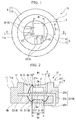
- FIG. 1 is a plan view showing a pressure sensor 10 which is a semiconductor pressure sensor according to a first embodiment of the invention (hereinbelow, simply referred to as a pressure sensor).
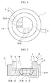
- FIG. 2 is a cross-sectional side view showing the pressure sensor 10.
- FIG. 3 is a development view showing the structure of a lead frame 4 used in the pressure sensor 10 as seen from the lower surface side of the lead frame 4.
- “upper” and “lower” correspond to the upper and lower positions in the vertical direction shown in FIG. 2 , respectively.
- the height direction means the upward direction shown in FIG. 2 .
- “plan view” means the plane that is seen from the thickness direction of the lead frame 4.
- the pressure sensor 10 includes: a base body 1, a pressure sensor chip 2 (pressure sensing device) provided on the base body 1, and a controller 3 (control device) built in the base body 1.
- the base body 1 includes: the lead frame 4; and a support 5 (package) that supports the lead frame 4 and is made of a resin.
- the lead frame 4 has a first surface and a second surface.
- the pressure sensor chip 2 is provided on first surface of the lead frame 4.
- the controller 3 is provided on the second surface of the lead frame 4.
- the support 5 includes: a base 6 formed in a circular shape in plan view; and a mounting portion 7 on which the pressure sensor chip 2 is mounted.
- the base 6 includes: a base body 11, and an annular wall 12 that protrudes upward from an upper surface 11a of the base body 11.
- the annular wall 12 can be formed integrally with the base body 11.
- the annular wall 12 shown as an example in the drawing is formed in a cylindrical shape.
- the internal space of the annular wall 12 is a container 9 that accommodates the pressure sensor chip 2 and a protective material 8 therein.
- the container 9 is a cylindrical-shaped space that is partitioned by the annular wall 12.
- a bottom surface 9a of the container 9 be located at the position which is lower than the upper surface 11a of the base body 11 outside the annular wall 12.
- the annular wall 12 can be formed to protrude upward so as to reach the position which is upper than the upper surface 2a of the pressure sensor chip 2. Consequently, it is possible to prevent the pressure sensor chip 2 from being affected by an external force.
- the base 6 can be formed by an integral molding by use of a resin.
- a resin used to form the base 6 is, for example, an epoxy resins; and the Young's modulus of the resin is, for example, 1GPa to 50GPa (preferably, 10GPa to 30GPa).
- the shape of the base 6 and the annular wall 12 which are shown as an example in the drawing is a circular shape in plan view; however, the shape of the base 6 and the annular wall 12 in plan view is not limited to those shape, an arbitrary shape such as a rectangular shape or other polygonal shapes can be adopted.
- the internal space of the annular wall 12 has the shape corresponding to the inner surface shape of the annular wall 12 in plan view.
- the shape of the container 9 is also a rectangular shape in plan view.
- the mounting portion 7 can be formed on part of the region of or the entire region of the bottom surface 9a so as to have a substantially constant thickness.
- the mounting portion 7 shown as an example in the drawing is formed on part of the region of the bottom surface 9a.
- the material used to form the mounting portion 7 is the same as the resin material used to form the base 6.
- the mounting portion 7 may be formed of a material having a hardness lower than that of the base 6.
- the mounting portion 7 using the same material as the resin material used to form the base 6, the resin material having hardness lower than that of the base 6 may be provided between the mounting portion 7 and the pressure sensor chip 2. Even in this case, an external force which is applied to the pressure sensor chip 2 due to the thermal expansion or the like of the base 6 is relieved, and it is possible to improve the measurement accuracy of the pressure sensor 10.
- the lead frame 4 is formed of an electrical conductor such as a metal.
- the lead frame 4 includes: a tabular pedestal 21 formed in a rectangular shape in plan view; sensor leads 22 that extend in the direction such that the sensor leads become far from the pedestal 21 in a plane parallel to the pedestal 21; and terminal leads 23 that extend in the direction such that the terminal leads become far from the pedestal 21.
- the sensor leads 22 includes: first sensor leads 22a, second sensor leads 22b, and third sensor leads 22c.
- the first sensor leads 22a, the second sensor leads 22b, and the third sensor leads 22c can be formed vertical to the first side edge 21a, the second side edge 21b, and the third side edge 21c of the pedestal 21 formed in a rectangular shape in plan view, respectively.
- the first sensor leads 22a, the second sensor leads 22b, and the third sensor leads 22c may be formed so as to be inclined with respect to the first side edge 21a, the second side edge 21b, and the third side edge 21c, respectively, at a predetermined angle (more than 0 degrees to less than 90 degrees).
- the first sensor lead 22a, the second sensor lead 22b, and the third sensor lead 22c are connected to the pressure sensor chip 2 via the respective bonding wires 13 (pressure sensor chip bonding wires) and are connected to the controller 3 via bonding wires 14 (controller bonding wires).
- part of the upper surface of the sensor lead 22 may be exposed at the bottom surface 9a of the container 9.
- the pedestal 21 may be or may not be exposed at the bottom surface 9a of the container 9. In the drawing shown as an example, since the pedestal 21 is covered with the mounting portion 7, the pedestal is not exposed.
- the terminal leads 23 can be formed perpendicular to the fourth side edge 21d of the pedestal 21 in plan view.
- the terminal leads 23 may be formed so as to be inclined with respect to the fourth side edge 21d at a predetermined angle (exceeds 0 degrees, less than 90 degrees).
- the terminal lead 23 shown as an example in the drawing includes: a base-extending portion 23a that extends in the direction such that base-extending portion becomes far from the pedestal 21; an intermediate-extending portion 23b that extends downward from the extending end of the base-extending portion 23a; and an outer extending portion 23c that extends from the extending end of the intermediate-extending portion 23b in the direction opposite to the extending direction of the base-extending portion 23a.
- the base-extending portion 23a and the intermediate-extending portion 23b can be formed and implanted into the inside of the support 5.
- the base-extending portion 23a is connected to the controller 3 via the bonding wire 15 (controller bonding wire).
- the outer extending portion 23c is exposed at the lower surface 6b of the base 6 and is formed along the lower surface 6b.
- the leads 22 and 23 are implanted in the base 6 with the exception of the outer extending portion 23c.
- the lead frame 4 is formed of a plate material which is made of a metal or the like, the lead frame has a certain measure of surface area and a high degree of rigidity, and therefore it is advantageous to prevent infiltration of water passing through the container 9.
- the lead frame 4 has excellent thermal conductivity, overheating or supercooling of the pressure sensor chip 2 and the controller 3 is prevented, and it is advantageous to stabilize the operations of the pressure sensor chip 2 and the controller 3.
- the terminal leads 23 are formed to be bent in this example; however, the terminal leads may be formed in a shape in which a bend portion is not formed (linear). In this case, the terminal leads 23 do not protrude from the lower surface 6b of the base 6 and protrude from the side surface thereof.
- a structure can be used which includes: a diaphragm; a sealed space serving as a reference pressure chamber; and a plurality of strain gauges that measure a variation in the strain resistance of the diaphragm due to a pressure, which are provided on one surface of a semiconductor substrate made of silicon or the like.
- the respective strain gauges can be electrically connected to the respective leads 22a to 22c and 23.
- the pressure sensor chip 2 described in this example when the diaphragm receives a pressure and is thereby bent, the stress corresponding to the amount of strain of the diaphragm is applied to each strain gauge, the resistance value of the strain gauge varies depending on this stress, and the sensor signal corresponding to the variation in the resistance value is thereby output.
- This pressure sensor chip 2 is a pressure sensor chip utilizing MEMS (Micro Electro-Mechanical Systems) technology.
- the pressure sensor chip 2 is accommodated in the container 9, mounted on the mounting portion 7, and is fixed to the mounting portion 7.
- the pressure sensor chip 2 is provided on the upper surface side (first surface) of the lead frame 4. Particularly, the pressure sensor chip 2 is provided at the position close to the upper surface 21e of the pedestal 21 along the upper surface 21e.
- part of the region or the entire region of the pressure sensor chip 2 may be provided at the position apart from the lead frame 4 in plan view.
- the pressure sensor chip 2 shown as an example in the drawing is provided on the pedestal 21 with the mounting portion 7 interposed therebetween.
- the bonding wire 13 is connected to the upper surface 2a of the pressure sensor chip 2.
- the width W1 of the pressure sensor chip 2 can be slightly smaller than the width W2 of the pedestal 21 of the lead frame 4 shown in FIGS. 2 and 3 .
- the length L1 of the pressure sensor chip 2 can be slightly smaller than the length L2 of the pedestal 21 of the lead frame 4 shown in FIG. 3 .
- the pressure sensor chip 2 is formed within the range that is included in the range in which the pedestal 21 is formed in plan view.
- the width of the pressure sensor chip 2 may be equal to the width of the pedestal 21 or greater than the width of the pedestal 21.
- the length of the pressure sensor chip 2 may be equal to the length of the pedestal 21 or greater than the length of the pedestal 21.
- the pressure sensor chip 2 be covered with the protective material 8 filling the container 9.
- the protective material 8 prevents infiltration of water or external air and can prevent any negative effect on the pressure sensor chip 2.
- the protective material 8 for example, a silicon based resin (for example, silicone resin) or a fluorine based resin can be used.
- a liquiform or a gel state protective material can be used. It is preferable that the protective material 8 have a high degree of viscosity.
- the protective material 8 it is preferable to use, for example, a soft gel agent having approximately zero hardness (Shore A hardness, in compliance with JIS K 6253).
- the protective material 8 can directly transmit, to the pressure sensor chip 2, a pressure applied from a measurement object. Consequently, the accuracy of detecting a pressure by the pressure sensor chip 2 is not degraded.
- the protective material 8 have a low degree of optical transparency. For this reason, since it is possible to block visible light or ultraviolet light, it is advantageous to prevent the pressure sensor chip 2 from being deteriorated.
- the optical transparency of the protective material 8 can be lowered by adding pigment or the like thereto.
- the controller When a sensor signal output from the pressure sensor chip 2 is input to the controller 3 through the bonding wire 13, the lead frame 4, and the bonding wires 14 and 15, the controller processes the output sensor signal and can output the signal as a pressure detection signal.
- the controller 3 has functions of, for example, controlling ON/OFF of the pressure sensor chip 2, correcting a detected value by a temperature sensor built therein, A/D conversion of detection data, correction of linearity, shaping a signal waveform, or the like.
- the controller 3 is provided at the lower surface side (second surface) of the lead frame 4. Particularly, the controller 3 is provided at the position close to the lower surface 21f of the pedestal 21 along the lower surface 21f.
- controller 3 is provided at the same position as that of the lower surface of the lead frame 4 or the position lower than the lower surface, part of the region or the entire region of the controller 3 may be provided at the position apart from the lead frame 4 in plan view.
- the width W3 of the controller 3 can be slightly smaller than the width W2 of the pedestal 21 of the lead frame 4.
- the length L3 of the controller 3 can be slightly smaller than the length L2 of the pedestal 21 of the lead frame 4.
- the controller 3 is formed within the range that is included in the range in which the lead frame 4 is formed in plan view.
- the width of the controller 3 may be equal to the width of the pedestal 21 or greater than the width of the pedestal 21.
- the length of the controller 3 may be equal to the length of the pedestal 21 or greater than the length of the pedestal 21.
- a temperature sensor may be built in the controller 3.
- the controller 3having the temperature sensor built therein can correct a pressure detection signal depending on a temperature inside of a system. Accordingly, pressure measurement with a high degree of accuracy is possible.
- the controller 3 is implanted into the support 5 (the base 6) and is formed integrally with the support 5. Since the outer surface of the controller 3 is covered, the controller 3 blocked from external air or moisture, it is possible to protect the controller 3.
- the controller 3 is positioned so as to overlap the pressure sensor chip 2 in plan view.
- part of the center region of the controller 3 is located at the position that overlaps the pressure sensor chip 2. Because of this, the controller 3 contains the entirety of the pressure sensor chip 2 in plan view.
- the part of the center region of the controller 3 overlaps the entire region of the pressure sensor chip 2 in plan view; however, the part of the region of the controller 3 may overlap part of the region of the pressure sensor chip 2, or the entire region of the controller 3 may be located at the position that overlaps part of the region or the entire region of the pressure sensor chip 2.
- the controller 3 Since the controller 3 has a lower surface 3a on which a circuit is formed, the bonding wires 14 and 15 are connected to the lower surface 3a.
- the circuit is formed on the upper surface 2a of the pressure sensor chip 2 that is provided on the upper surface side of the lead frame 4.
- the circuit is formed on the lower surface 3 a of the controller 3 that is provided on the lower surface side of the lead frame 4. Consequently, the interconnection length is shortened and it is possible to reduce the effect of noise generated from external side.
- the controller 3 is mounted on the pedestal 21 of the lead frame 4 and is connected to the leads 22 and 23 via the bonding wires 14 and 15.
- the support 5 is formed by resin-molding or the like. Consequently, the controller 3 and the bonding wires 14 and 15 are implanted into the support 5 and are thereby in a state of not being exposed to the external side.
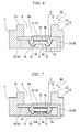
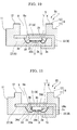
- Part of the upper surface of the lead frame 4 (for example, part of the upper surface of the sensor lead 22 shown in FIG. 4 ) may be exposed to the inside of the container 9.
- the pedestal 21 may be or may not be exposed. In the drawing shown as an example, the pedestal 21 is covered with the mounting portion 7.
- the pressure sensor chip 2 is provided on the mounting portion 7, and the pressure sensor chip 2 is connected to the sensor leads 22 with the bonding wires 13 interposed therebetween.
- the pressure sensor chip 2 is covered with the protective material 8 by filling the container 9 therewith.
- the controller 3 and the pressure sensor chip 2 are located so that the controller at least partially overlaps the pressure sensor chip, it is possible to reduce the total space which is occupied by the pressure sensor chip 2 and the controller 3. Consequently, it is possible to reduce the pressure sensor 10 in size.
- the pressure sensor 10 since the pressure sensor chip 2 comes close to the controller 3, the lengths of the electrical wirings (the bonding wires 13 to 15 or the like) which are connected to the pressure sensor chip 2 and the controller 3 become shortened. For this reason, it is possible to improve the resistance to electromagnetic noise, and it is possible to improve the detection accuracy.
- the pressure sensor chip 2 is located adjacent to the controller 3, it is possible to reduce the difference in temperature between the pressure sensor chip 2 and the controller 3. Accordingly, in the case where the controller 3 is provided with a temperature sensor, a detected value of the pressure sensor is stabilized, and it is possible to improve the accuracy thereof.
- the controller 3 since the controller 3 is implanted in the support 5 made of a resin, it is possible to realize the configuration in which the wirings (for example, the bonding wires 14 and 15) of the controller 3 to which a high voltage is applied are not exposed, the durability thereof is improved, and it is possible to ensure a long-term reliability.
- connection reliability between the pressure sensor chip 2 and the lead frame 4 and between the controller 3 and the lead frame 4 is improved by use of the bonding wires 13 to 15, and it is possible to detect a pressure with a high degree of accuracy.
- FIG. 6 shows a cross-sectional side view showing a pressure sensor 30 serving as a pressure sensor according to a second embodiment of the invention.
- FIGS. 6 to 11 the pressure sensor chip 2 and the protective material 8 are not shown in the drawings, and the structure according to the aforementioned first embodiment is adopted.
- identical reference numerals are used for the elements which are common to the aforementioned pressure sensor, and the explanations thereof are omitted or simplified here.
- the pressure sensor 30 preferably uses the controller 3 including a temperature sensor.
- a structure can be adopted which includes: a temperature sensor 31 that measures an outside temperature; an A/D converter (not shown in the figure) that A/D-converts a signal output from the temperature sensor 31 and outputs the signal as a temperature signal; and a processor (not shown in the figure) to which the temperature signal is input.
- the processor can carry out a process of correcting the sensor signal output from the pressure sensor chip 2.
- thermocouple temperature sensor As the temperature sensor 31, a resistance-type temperature sensor (bridge resistance type), a diode-type temperature sensor, a thermocouple temperature sensor, an infrared light temperature sensor, or the like is adopted.
- a rectangular parallelepiped shape can be adopted which includes: a rectangular-shaped bottom surface 3b; side surfaces 3c formed on the respective peripheral edge portions that correspond to four side portions of the bottom surface 3b; and an outer surface 3a (the lower surface 3a). That is, the controller 3 is formed in the shape having a plurality of surfaces.
- the temperature sensor 31 can be provided at the position that is inside the controller 3 and is adjacent to the outer surface 3a (the lower surface 3a).
- a stress relief layer 32 including a material having a low Young's modulus (Young's modulus lower than that of the support 5) is formed on the bottom surface 3b of the controller 3 (at least one of the plurality of surfaces).
- the stress relief layer 32 (inner-face stress relief layer 32) shown as an example in the drawing covers the entire area of the bottom surface 3b of the controller 3 and is interposed between the lead frame 4 (the pedestal 21) and the controller 3. Accordingly, the bottom surface 3b is apart from the lead frame 4.
- the stress relief layer 32 shown as an example in the drawing is formed so as to have a constant thickness.
- the Young's modulus of the stress relief layer 32 is lower than the Young's modulus of the base 6 (the support 5). Also, the stress relief layer 32 is lower than the lead frame 4 in Young's modulus.
- the outer surface 3a (the lower surface 3a) and the side surfaces 3c of the controller 3 is in contact with the base 6.
- the stress relief layer 32 may be formed on only part of the bottom surface 3b.
- a material having a low Young's modulus used to form the stress relief layer 32 a material can be used which has the Young's modulus in the case where after curing is subjected thereto lower than the Young's modulus of the material used to form the base 6, for example, a thermosetting resin, a ultraviolet curable resin, or the like can be used.
- a silicone resin, epoxy-based resins, urethane resins, poly imide resins, or the like can be used.
- the material having a low Young's modulus one of the above-mentioned materials may be used, or two or more thereof may be concomitantly used. Above all, particularly, since a silicone resin is difficult to absorb moisture, it is preferable in that the physical properties thereof are difficult to vary even in a high temperature and high humidity environment.
- the Young's modulus of the stress relief layer 32 is preferably, for example, 1 MPa to 500 MPa (more preferably, 1 MPa to 100 MPa).
- the Young's modulus of the stress relief layer 32 be less than or equal to 1/10 (more preferably, 1/100 or less) of the Young's modulus of the material used to form the base 6.
- the Young's modulus can be measured by methods of JIS K 7161, JIS K 7244.
- the thickness of the stress relief layer 32 can be, for example, 5 to 100 ⁇ m (preferably, 10 to 50 ⁇ m). By setting the thickness of the stress relief layer 32 to be 5 ⁇ m or more, a high degree of stress relief effect can be obtained. Furthermore, by setting the thickness to be 100 ⁇ m or less, the entire thickness can be reduced.
- the same configuration as that of the pressure sensor 10 according to the first embodiment shown in FIG. 2 or the like may be adopted with the exception that the stress relief layer 32 (inner-face stress relief layer 32) is provided.
- An uncured (liquiform) material having a low Young's modulus is supplied to the controller 3 or the pedestal 21 by a dispenser or the like, the material is cured by heating or the like, and the stress relief layer 32 is thereby formed.
- the controller 3 is connected to the leads 22 and 23 via the bonding wires 14 and 15, respectively.
- the support 5 is formed by resin-molding or the like.
- the pressure sensor chip 2 is provided on the mounting portion 7, the pressure sensor chip 2 is connected to the sensor lead 22 via the bonding wire 13.
- the pressure sensor chip 2 is covered with the protective material 8 by filling the container 9 therewith. Consequently, the pressure sensor 30 is obtained.
- the stress relief layer 32 can also be formed by attaching a sheet made of a material having a low Young's modulus to the controller 3 or the pedestal 21.
- the bottom surface 3b of the controller 3 is in contact with the stress relief layer 32. Consequently, a stress generated from peripheral components around the controller 3 (the base 6, the lead frame 4) is released, therefore, an error of output from the temperature sensor 31 of the controller 3 can be avoided from increasing, and therefore it is possible to improve measurement accuracy of the pressure sensor 30.
- this effect will be particularly described.
- a stress generated when a resin is cured or a heat stress or the like generated due to a difference in temperature between a curing temperature and a room temperature is applied to the base 6 or the like.
- the base 6 or the like is likely to be deformed.
- the lead frame 4 is also deformed.
- the base 6 easily absorbs moisture in a high temperature and high humidity environment, the above-described deformation is likely to occur.
- the controller 3 since the controller 3 is in contact with the stress relief layer 32 made of a material having a low Young's modulus, it is possible to reduce a pressure to the controller 3 by deformation of the base 6 and the lead frame 4.
- FIG. 7 is a cross-sectional side view showing a pressure sensor 40 serving as a pressure sensor according to a third embodiment of the invention.
- the pressure sensor 40 described in this example is different from the pressure sensor 30 according to the second embodiment shown in FIG. 6 in that a stress relief layer is formed not only on the bottom surface 3b of the controller 3 but also on the outer surface 3a (the lower surface 3a).
- the inner-face stress relief layer 32 is formed on the bottom surface 3b of the controller 3, and an outer-face stress relief layer 33 is formed on the outer surface 3a (the lower surface 3a, at least one of the plurality of surfaces) of the controller 3.
- the outer-face stress relief layer 33 is formed to cover the entire area of the outer surface 3a (the lower surface 3a) and is interposed between the outer surface 3a (the lower surface 3a) and the base 6. Consequently, the outer surface 3a (the lower surface 3a) is separated from the base 6.
- the Young's modulus of the outer-face stress relief layer 33 is lower than the Young's modulus of the base 6. Particularly, the Young's modulus of the outer-face stress relief layer 33 is lower than the Young's modulus of the base 6 at the portion which faces the outer surface 3a of the controller 3 (the lower surface 3a) with the outer-face stress relief layer 33 interposed therebetween.
- the base 6 is a member that is in contact with the controller 3. Therefore, as compared with the case where the outer-face stress relief layer 33 is not formed, the outer surface 3a of the controller 3 (the lower surface 3a) is in touch with a member having a low Young's modulus.
- the pressure sensor 40 may have the same configuration as that of the pressure sensor 30 shown in FIG. 6 with the exception that the outer-face stress relief layer 33 is provided.
- the outer-face stress relief layer 33 may be formed on only part of the outer surface 3a (the lower surface 3a) and may be formed in, for example, a shape including the portion that overlaps the temperature sensor 31 in plan view.
- a material having a low Young's modulus (silicone resin or the like) which is adopted as the preferred material associated with the stress relief layer 32 of the pressure sensor 30 according to the second embodiment can be used.
- the Young's modulus of the outer-face stress relief layer 33 and the Young's modulus ratio thereof to the base 6 it is preferable to adopt a preferred range which is associated with the stress relief layer 32 of the pressure sensor 30 according to the second embodiment.
- the material used to form the outer-face stress relief layer 33 may be the same as the material used to form the stress relief layer 32 (the inner-face stress relief layer 32) or may be different from the stress relief layer 32.
- the thickness (average thickness) of the outer-face stress relief layer 33 can be, for example, 5 ⁇ m to 400 ⁇ m (preferably, 100 ⁇ m to 400 ⁇ m). By setting the thickness to be 5 ⁇ m or more, a high degree of stress relief effect can be obtained. Furthermore, by setting the thickness to be 400 ⁇ m or less, the entire thickness can be reduced.
- the outer surface 33a of the outer-face stress relief layer 33 is preferably a curved convex surface.
- the curved convex surface is, for example, a spherical surface, ellipsoidal spherical surface, or the like.
- the entire surface thereof may be a curved convex surface or only part thereof may be a curved convex surface.
- the cross-sectional shape of the outer surface 33a forming the curved convex surface may be, for example; a circular arc shape: a high-order curve shape (for example, quadratic curve shape) such as an ellipse arc shape, a parabolic shape, or a hyperbolic shape; or the like.
- a circular arc shape for example, a high-order curve shape (for example, quadratic curve shape) such as an ellipse arc shape, a parabolic shape, or a hyperbolic shape; or the like.
- the thickness thereof gradually varies so that the thickness thereof is largest at the center of the outer-face stress relief layer 33 and the thickness becomes thin at the position close to the circumferential edge of the outer-face stress relief layer 33.
- the outer surface 33a has the curved convex surface and a stress is less easily concentrated, the degree of the effect of reducing the influence of the deformation of the base 6 or the like on the controller 3 is increased, and it is possible to prevent an occurrence of an output error in the temperature sensor 31.
- the outer surface 33a is the curved convex surface, a resin smoothly flows in a die during molding the base 6 by filling a die with the resin.
- the stress relief layer 32 is formed, the controller 3 is connected to the leads 22 and 23 via the bonding wires 14 and 15, respectively, thereafter, a material having a low Young's modulus is supplied to the outer surface 3a of the controller 3 (the lower surface 3a), the material is cured, and the outer-face stress relief layer 33 is thereby formed.
- the method which supplies a uncured material having a low Young's modulus by use of a dispenser or the like, cures the material, and thereby forms a stress relief layer is preferable in that it is possible to form the outer-face stress relief layer 33 on a larger region such as the outer surface 3a (the lower surface 3a), as compared with a method of attaching a preliminarily-cured sheet thereto.
- the support 5 is formed by resin-molding or the like, the pressure sensor chip 2 is provided thereon, the inside of the container 9 is filled with the protective material 8, and the pressure sensor 40 is thereby obtained.
- the outer-face stress relief layer 33 is formed not only on the bottom surface 3b of the controller 3 but also on the outer surface 3a (the lower surface 3a).
- the stress relief layer is formed on a large surface area, the degree of the effect of reducing the influence of the deformation of the base 6 or the like on the controller 3 is increased, it is possible to prevent an occurrence of an output error in the temperature sensor 31.
- the stress relief layer 33 is formed between the lead frame 4 and the base 6 that is made of a resin and is thereby likely to be deformed by moisture absorbing, the degree of the effect of preventing the influence of the deformation is improved as compared with the pressure sensor 30 having the stress relief layer 32 formed between the base 6 and the lead frame 4.
- FIG. 8 is a cross-sectional side view showing a pressure sensor 50 serving as a pressure sensor according to a fourth embodiment of the invention.
- the pressure sensor 50 described in this example is different from the pressure sensor 30 according to the second embodiment shown in FIG. 6 in that a stress relief layer is formed not only on the bottom surface 3b of the controller 3 but also on the side surface 3c.
- the inner-face stress relief layer 32 is formed on the bottom surface 3b of the controller 3, and a side-face stress relief layer 34 is formed on the side surface 3c (at least one of the plurality of surfaces) of the controller 3.
- the pressure sensor 50 may have the same configuration as that of the pressure sensor 30 shown in FIG. 6 with the exception that the side-face stress relief layers 34 is provided.
- the side-face stress relief layers 34 is formed to cover the entire area of the side surfaces 3c and is interposed between the side surfaces 3c and the base 6. For this reason, the side surface 3c is separated from the base 6.
- the side-face stress relief layers 34 can be formed integrally with the inner-face stress relief layer 32.
- the side-face stress relief layers 34 may be formed on only part of the side surface 3c. In this case, it is preferable that 50 to 95% of the side surface 3c of the controller 3 be covered with the side-face stress relief layers 34.
- a material having a low Young's modulus (silicone resin or the like) which is adopted as the preferred material associated with the stress relief layer 32 of the pressure sensor 30 according to the second embodiment can be used.
- the Young's modulus of the side-face stress relief layers 34 and the Young's modulus ratio thereof to the base 6 it is preferable to adopt a preferred range which is associated with the stress relief layer 32 of the pressure sensor 30 according to the second embodiment.
- the thickness (average thickness) of the side-face stress relief layers 34 can be, for example, 5 ⁇ m to 500 ⁇ m (preferably, 50 ⁇ m to 300 ⁇ m).
- the thickness of the stress relief layer 32 can be 5 ⁇ m or more, a high degree of stress relief effect can be obtained. Furthermore, by setting the thickness to be 500 ⁇ m or less, the entire thickness can be reduced.
- the stress relief layer 32 is formed, a material having a low Young's modulus is supplied to the side surface 3c of the controller 3, the material is cured, and the side-face stress relief layers 34 is thereby formed.
- the controller 3 is connected to the leads 22 and 23 via the bonding wires 14 and 15, respectively.
- the support 5 is formed by resin-molding or the like, the pressure sensor chip 2 is provided thereon, the inside of the container 9 is filled with the protective material 8, and the pressure sensor 50 is thereby obtained.
- a method of forming the side-face stress relief layers 34 a method can be adopted which determines the supply amount of a material having a low Young's modulus used to form the stress relief layer 32 to be greater than a required amount, allows the material having a low Young's modulus to overflow from between the bottom surface 3b of the controller 3 and the lead frame 4 when the controller 3 is provided, and thereby forms the side-face stress relief layers 34 by the overflowed portion.
- the stress relief layers 34 is formed not only on the bottom surface 3b of the controller 3 but also on the side surface 3c, the degree of the effect of reducing the influence of the deformation of the base 6 or the like on the controller 3 is increased, and it is possible to prevent an occurrence of an output error in the temperature sensor 31.
- FIG. 9 is a cross-sectional side view showing a pressure sensor 60 serving as a pressure sensor according to a fifth embodiment of the invention.
- the pressure sensor 60 described in this example is different from the pressure sensor 30 according to the second embodiment shown in FIG. 6 in that a stress relief layer 35 is formed to cover the bottom surface 3b, the side surfaces 3c, and the outer surface 3a (the lower surface 3a) of the controller 3.
- the stress relief layer 35 includes: an inner-face stress relief layer 35b that covers the bottom surface 3b of the controller 3; a side-face stress relief layer 35c that covers the side surfaces 3c; and an outer-face stress relief layer 35a that covers the outer surface 3a (the lower surface 3a).
- the stress relief layers 35b, 35c, and 35a can be integrally formed into a body.
- the stress relief layer 35 has: an inner surface 35d that comes into contact with the lead frame 4; and an outer surface 35e that comes into contact with the base 6.
- the stress relief layer 35 is formed to cover the entire surface of the controller 3, the controller 3 arranged separately from the base 6 and the lead frame 4.
- the outer surface 35e of the stress relief layer 35 be a curved convex surface.
- the entire surface thereof may be a curved convex surface or only part thereof may be a curved convex surface.
- the thickness thereof gradually varies so that the thickness thereof is largest at the center of the stress relief layer 35 and the thickness becomes thin at the position close to the circumferential edge of the stress relief layer 35.
- the outer surface 35e of the stress relief layer 35 is the curved convex surface, a stress is less easily concentrated.
- the outer surface 35e of the stress relief layer 35 is the curved convex surface, a stress that is transmitted from the base 6 to the stress relief layer 35 is uniformly applied to the entire surface of the curved outer surface 35e of the stress relief layer 35. For this reason, the degree of the effect of reducing the influence of the deformation of the base 6 or the like on the controller 3 is increased, and it is possible to prevent an occurrence of an output error in the temperature sensor 31.
- the outer surface 35e is the curved convex surface, a resin smoothly flows in a die during molding the base 6 by filling a die with the resin.
- the pressure sensor 60 may have the same configuration as that of the pressure sensor 30 shown in FIG. 6 with the exception that the stress relief layer 35 is provided.
- the stress relief layer 35 a material having a low Young's modulus (silicone resin or the like) which is adopted as the preferred material associated with the stress relief layer 32 of the pressure sensor 30 according to the second embodiment can be used.
- the Young's modulus of the stress relief layer 35 and the Young's modulus ratio thereof to the base 6 it is preferable to adopt a preferred range which is associated with the stress relief layer 32 of the pressure sensor 30 according to the second embodiment.
- the pressure sensor 60 can be manufactured by combining the methods of manufacturing the aforementioned pressure sensors 30 to 50. For example, the following manufacturing method is possible.
- a material having a low Young's modulus is supplied to the controller 3 or the pedestal 21 by a dispenser or the like, the material is cured by heating or the like, the inner-face stress relief layer 35b is thereby formed, and also the material having a low Young's modulus is supplied to the side surfaces 3c of the controller 3, and the side-face stress relief layer 35c is thereby formed.
- the controller 3 is connected to the leads 22 and 23 via the bonding wires 14 and 15, respectively, thereafter, the material having a low Young's modulus is supplied to the outer surface 3a of the controller 3 (the lower surface 3a), and the outer-face stress relief layer 35a is thereby formed.
- the support 5 is formed by resin-molding or the like, the pressure sensor chip 2 is provided thereon, the inside of the container 9 is filled with the protective material 8, and the pressure sensor 60 is thereby obtained.
- a method of forming the side-face stress relief layer 35c As a method of forming the side-face stress relief layer 35c, a method can be adopted which determines the supply amount of a material having a low Young's modulus used to form the inner-face stress relief layer 35b to be greater than a required amount, allows the material having a low Young's modulus to overflow from between the bottom surface 3b of the controller 3 and the lead frame 4 when the controller 3 is provided, and thereby forms the side-face stress relief layer 35c by the overflowed portion.
- the stress relief layer 35 is formed to cover the entire surface of the controller 3, the degree of the effect of reducing the influence of the deformation of the base 6 or the like on the controller 3 is further increased, and it is possible to prevent an occurrence of an output error in the temperature sensor 31.
- FIG. 10 is a cross-sectional side view showing a pressure sensor 70 serving as a pressure sensor according to a sixth embodiment of the invention.
- the pressure sensor 70 described in this example is different from the pressure sensor 40 according to the third embodiment shown in FIG. 7 in that the inner-face stress relief layer 32 is not formed on the bottom surface 3b of the controller 3.
- the outer-face stress relief layer 33 is formed on the outer surface 3a (the lower surface 3a) that is located near the temperature sensor 31, the degree of the effect of reducing the influence of the deformation of the base 6 or the like on the controller 3 is increased, and it is possible to prevent an occurrence of an output error in the temperature sensor 31.
- FIG. 11 is a cross-sectional side view showing a pressure sensor 80 serving as a pressure sensor according to a seventh embodiment of the invention.
- the pressure sensor 80 described in this example is different from the pressure sensor 60 according to the fifth embodiment shown in FIG. 9 in that a stress relief layer is not formed on the bottom surface 3b of the controller 3.
- a stress relief layer 36 includes: a side-face stress relief layer 36c that covers the side surfaces 3c of the controller 3; and an outer-face stress relief layer 36a that covers the outer surface 3a (the lower surface 3a).
- the stress relief layers 36c and 36a can be integrally formed into a body.
- the stress relief layer 36 has: an inner surface 36d that comes into contact with the lead frame 4; and an outer surface 36e that comes into contact with the base 6.
- the controller 3 is separated from the base 6.
- the outer surface 36e of the stress relief layer 36 be a curved convex surface.
- the stress relief layer 36 since the stress relief layer 36 is formed, the degree of the effect of reducing the influence of the deformation of the base 6 or the like on the controller 3 is further increased, it is possible to prevent an occurrence of an output error in the temperature sensor 31.
- the pressure sensor 10 shown in FIGS. 1 and 2 was manufactured as follows.
- a controller was used which includes: the temperature sensor 31 (refer to FIG. 6 ); an A/D converter that A/D-converts a signal output from the temperature sensor 31 and outputs the signal as a temperature signal; and a processor that carries out a process of correcting the sensor signal output from the pressure sensor chip 2 based on the temperature signal.
- the controller 3 was mounted on the pedestal 21 of the lead frame 4 and was connected to the leads 22 and 23 via the bonding wires 14 and 15, respectively.
- the support 5 was formed by resin-molding.
- the pressure sensor chip 2 was disposed on the mounting portion 7, the pressure sensor chip 2 was connected to the sensor leads 22 via the bonding wires 13, thereafter the inside of the container 9 was filled with the protective material 8, and thereby the pressure sensor 10 was obtained.
- the pressure sensor 30 shown in FIG. 6 was manufactured.
- the stress relief layer 32 was formed by supplying an uncured silicone resin by a dispenser, and the silicone resin was cured by heating or the like, and the silicone resin was thereby formed.
- the thickness of the stress relief layer 32 was 10 ⁇ m.
- the configuration was the same as that of Example 1 except for the stress relief layer 32.
- the pressure sensor 40 shown in FIG. 7 was manufactured.
- the stress relief layers 32 and 33 were formed of silicone resin in a way similar to the case of Example 2.
- the outer surface 33a of the outer-face stress relief layer 33 was formed in a curved convex surface shape.
- the thickness (average thickness) of the outer-face stress relief layer 33 was 200 ⁇ m.
- the configuration was the same as that of Example 2 except for the stress relief layer 33.
- the pressure sensor 50 shown in FIG. 8 was manufactured.
- the stress relief layers 32 and 34 were formed of silicone resin in a way similar to the case of Example 2.
- the thickness (average thickness) of the side-face stress relief layers 34 was 100 ⁇ m.
- the configuration was the same as that of Example 2 except for the stress relief layer 34.
- the pressure sensor 60 shown in FIG. 9 was manufactured.
- the stress relief layer 35 was formed of silicone resin in a way similar to the case of Example 2.
- the thickness of the stress relief layer 35b was the same as the thickness of the stress relief layer 32 Example 2.
- the thickness (average thickness) of the stress relief layer 35c was the same as the thickness of the stress relief layers 34 of Example 3.
- the thickness (average thickness) of the stress relief layer 35a was the same as the thickness of the stress relief layer 33 of Example 4.
- the configuration was the same as that of Example 1 except for the stress relief layer 35.
- Example 5 in which the stress relief layer 35 that covers the entire surface of the controller 3 is provided, it is possible to reduce the error of output thereof. As a result, it was possible to improve the measurement accuracy of the pressure sensor of Example 5.
- the shape (outer shape) of the controller is not limited to the rectangular parallelepiped shape (hexahedron) and may be other polyhedron shape (the number of surfaces is greater than or equal to an arbitrary integer of 4).
- the shape of the controller is not limited to a polyhedron shape and may be formed in a shape having a plurality of surfaces and a shape having one or more curved surfaces of the plurality of the surfaces (a circular cylinder shape, a hemispherical shape, or the like).
- the stress relief layer can be formed on part of the region or the entire region of at least one of the surfaces of the controller having the plurality of the surfaces.
- the shape of the controller is not limited to the shape having the plurality of the surfaces. As long as the stress relief layer is formed on at least part of the surface of the controller, the aforementioned effect (reduction in an error of output of controller) is obtained.
- the regions on which the stress relief layers are formed are not limited to the regions shown in FIGS. 6 to 11 .
- the stress relief layer may be formed on only the side surface 3c.
Landscapes
- Physics & Mathematics (AREA)
- General Physics & Mathematics (AREA)
- Chemical & Material Sciences (AREA)
- Analytical Chemistry (AREA)
- Health & Medical Sciences (AREA)
- Child & Adolescent Psychology (AREA)
- Measuring Fluid Pressure (AREA)
- Pressure Sensors (AREA)
- Wire Bonding (AREA)
- Micromachines (AREA)
- Structures Or Materials For Encapsulating Or Coating Semiconductor Devices Or Solid State Devices (AREA)
Abstract
Description
- The present invention relates to a semiconductor pressure sensor which can be used in a portable device or the like, such as a wrist watch for divers provided with a water depth meter.
- This application claims priority from
Japanese Patent Application No. 2013-209568 filed on October 4, 2013 Japanese Patent Application No. 2014-045705 filed on March 7, 2014 - Conventionally, a small semiconductor pressure sensor (hereinbelow, simply referred to as a pressure sensor) which utilizes MEMS technology (Micro Electro-Mechanical Systems) is used in a portable device or the like (for example, refer to Patent Document 1).
- As this kind of pressure sensor, for example, a pressure sensor is known which has: a pressure sensor chip; and a controller that receives a sensor signal output from the pressure sensor chip and outputs a pressure detection.
- [Patent Document 1]
Japanese Patent No. 3620185 - In recent years, it is required to reduce the size of a pressure sensor with miniaturization of portable devices.
- The invention was made with respect to the above-described problems and has an object to provide a pressure sensor that can be reduced in size.
- A semiconductor pressure sensor according to one aspect of the invention includes: a base body including: a lead frame having a first surface and a second surface; and a support that supports the lead frame and is made of a resin; a pressure sensor chip provided on the first surface of the lead frame; and a controller that is provided on the second surface of the lead frame, is implanted in the support, is formed in the shape having a plurality of surfaces, includes a stress relief layer that is formed on at least one of the plurality of surfaces and has the Young's modulus lower than that of the support, and receives a sensor signal output from the pressure sensor chip and thereby outputs a pressure detection, the pressure sensor chip at least partially overlapping the controller in plan view.
- In the semiconductor pressure sensor according to one aspect of the invention, the stress relief layer may cover an entire surface of the controller.
- In the semiconductor pressure sensor according to one aspect of the invention, the stress relief layer may have an external surface forming a curved convex surface.
- In the semiconductor pressure sensor according to one aspect of the invention, the Young's modulus of the stress relief layer may be less than or equal to 1/10 of the Young's modulus of the support.
- In the semiconductor pressure sensor according to one aspect of the invention, each of the pressure sensor chip and the controller may be connected to the lead frame via a bonding wire.
- In the semiconductor pressure sensor according to one aspect of the invention, the support include: a base; and a mounting portion on which the pressure sensor chip is mounted, and the mounting portion may be formed of a material having a hardness lower than a material used to form the base.
- In the semiconductor pressure sensor according to one aspect of the invention, a container that accommodates the pressure sensor therein may be formed on the base, the container may be filled with a protective material that covers the pressure sensor chip, and the protective material may be capable of transmitting, to the pressure sensor chip, a pressure applied from a measurement object.
- In the semiconductor pressure sensor according to one aspect of the invention, the lead frame may be implanted in the support.
- According to one aspect of the invention, since the pressure sensor chip and the controller are located at the position at which, the pressure sensor chip at least partially overlaps the controller in plan view, it is possible to reduce the total space which is occupied by the pressure sensor chip and the controller. Consequently, it is possible to reduce the size of the pressure sensor.
- Moreover, since the pressure sensor chip is provided adjacent to the controller, an electrical wiring (bonding wire or the like) that connects the pressure sensor chip and the controller becomes shortened. For this reason, it is possible to improve the resistance to electromagnetic noise, and it is possible to improve the detection accuracy of the pressure sensor.
- In addition, since the pressure sensor chip is located adjacent to the controller, it is possible to reduce the difference in temperature between the pressure sensor chip and the controller. Accordingly, in the case where the controller is provided with a temperature sensor, a detected value of the pressure sensor is stabilized, and it is possible to improve the accuracy thereof.
-
-
FIG. 1 is a plan view showing a pressure sensor according to the first embodiment of the invention. -
FIG. 2 is a cross-sectional side view taken along the line I-I shown inFIG. 1 . -
FIG. 3 is a development view showing the structure of a lead frame used in the pressure sensor shown inFIG. 1 as seen from the lower surface side of the lead frame. -
FIG. 4 is a flow sheet showing a step of manufacturing the pressure sensor shown inFIG. 1 and is a plan view showing a pressure sensor before the pressure sensor chip is provided. -
FIG. 5 is a cross-sectional side view showing the pressure sensor in the step shown in the previous drawing. -
FIG. 6 is a cross-sectional side view showing a pressure sensor according to the second embodiment of the invention. -
FIG. 7 is a cross-sectional side view showing a pressure sensor according to the third embodiment of the invention. -
FIG. 8 is a cross-sectional side view showing a pressure sensor according to the fourth embodiment of the invention. -
FIG. 9 is a cross-sectional side view showing a pressure sensor according to the fifth embodiment of the invention. -
FIG. 10 is a cross-sectional side view showing a pressure sensor according to the sixth embodiment of the invention. -
FIG. 11 is a cross-sectional side view showing a pressure sensor according to the seventh embodiment of the invention. - Hereinafter, a first embodiment of the invention will be described based on preferred embodiment with reference to drawings.
-
FIG. 1 is a plan view showing apressure sensor 10 which is a semiconductor pressure sensor according to a first embodiment of the invention (hereinbelow, simply referred to as a pressure sensor).FIG. 2 is a cross-sectional side view showing thepressure sensor 10.FIG. 3 is a development view showing the structure of alead frame 4 used in thepressure sensor 10 as seen from the lower surface side of thelead frame 4. - In the following explanation, "upper" and "lower" correspond to the upper and lower positions in the vertical direction shown in
FIG. 2 , respectively. Furthermore, the height direction means the upward direction shown inFIG. 2 . As shown inFIGS. 1 and3 , "plan view" means the plane that is seen from the thickness direction of thelead frame 4. - As shown in
FIGS. 1 and 2 , thepressure sensor 10 includes: abase body 1, a pressure sensor chip 2 (pressure sensing device) provided on thebase body 1, and a controller 3 (control device) built in thebase body 1. - As shown in
FIGS. 2 and3 , thebase body 1 includes: thelead frame 4; and a support 5 (package) that supports thelead frame 4 and is made of a resin. - The
lead frame 4 has a first surface and a second surface. Thepressure sensor chip 2 is provided on first surface of thelead frame 4. Thecontroller 3 is provided on the second surface of thelead frame 4. - The
support 5 includes: abase 6 formed in a circular shape in plan view; and amounting portion 7 on which thepressure sensor chip 2 is mounted. - The
base 6 includes: abase body 11, and anannular wall 12 that protrudes upward from anupper surface 11a of thebase body 11. Theannular wall 12 can be formed integrally with thebase body 11. Theannular wall 12 shown as an example in the drawing is formed in a cylindrical shape. - The internal space of the
annular wall 12 is acontainer 9 that accommodates thepressure sensor chip 2 and aprotective material 8 therein. In the drawing shown as an example, thecontainer 9 is a cylindrical-shaped space that is partitioned by theannular wall 12. - As shown in
FIG. 2 , it is preferable that abottom surface 9a of thecontainer 9 be located at the position which is lower than theupper surface 11a of thebase body 11 outside theannular wall 12. - The
annular wall 12 can be formed to protrude upward so as to reach the position which is upper than theupper surface 2a of thepressure sensor chip 2. Consequently, it is possible to prevent thepressure sensor chip 2 from being affected by an external force. - The
base 6 can be formed by an integral molding by use of a resin. - A resin used to form the
base 6 is, for example, an epoxy resins; and the Young's modulus of the resin is, for example, 1GPa to 50GPa (preferably, 10GPa to 30GPa). - Particularly, the shape of the
base 6 and theannular wall 12 which are shown as an example in the drawing is a circular shape in plan view; however, the shape of thebase 6 and theannular wall 12 in plan view is not limited to those shape, an arbitrary shape such as a rectangular shape or other polygonal shapes can be adopted. The internal space of theannular wall 12 has the shape corresponding to the inner surface shape of theannular wall 12 in plan view. For example, in the case where the inner surface of theannular wall 12 is formed in a rectangular shape in plan view, the shape of thecontainer 9 is also a rectangular shape in plan view. - The mounting
portion 7 can be formed on part of the region of or the entire region of thebottom surface 9a so as to have a substantially constant thickness. The mountingportion 7 shown as an example in the drawing is formed on part of the region of thebottom surface 9a. - The material used to form the mounting
portion 7 is the same as the resin material used to form thebase 6. The mountingportion 7 may be formed of a material having a hardness lower than that of thebase 6. As a result of forming the mountingportion 7 by use of a resin material having a hardness lower than that of thebase 6, an external force which is applied to thepressure sensor chip 2 due to the thermal expansion or the like of thebase 6 is relieved, and it is possible to improve the measurement accuracy of thepressure sensor 10. As the thickness of the resin increases, the degree of the effect of relieving the external force increases. - Alternatively, by forming the mounting
portion 7 using the same material as the resin material used to form thebase 6, the resin material having hardness lower than that of thebase 6 may be provided between the mountingportion 7 and thepressure sensor chip 2. Even in this case, an external force which is applied to thepressure sensor chip 2 due to the thermal expansion or the like of thebase 6 is relieved, and it is possible to improve the measurement accuracy of thepressure sensor 10. - As shown in
FIG. 3 , thelead frame 4 is formed of an electrical conductor such as a metal. Thelead frame 4 includes: atabular pedestal 21 formed in a rectangular shape in plan view; sensor leads 22 that extend in the direction such that the sensor leads become far from thepedestal 21 in a plane parallel to thepedestal 21; and terminal leads 23 that extend in the direction such that the terminal leads become far from thepedestal 21. - As seen from a plan view, the sensor leads 22 includes: first sensor leads 22a, second sensor leads 22b, and third sensor leads 22c. The first sensor leads 22a, the second sensor leads 22b, and the third sensor leads 22c can be formed vertical to the first side edge 21a, the
second side edge 21b, and thethird side edge 21c of thepedestal 21 formed in a rectangular shape in plan view, respectively. The first sensor leads 22a, the second sensor leads 22b, and the third sensor leads 22c may be formed so as to be inclined with respect to the first side edge 21a, thesecond side edge 21b, and thethird side edge 21c, respectively, at a predetermined angle (more than 0 degrees to less than 90 degrees). - As shown in
FIG. 2 , the first sensor lead 22a, the second sensor lead 22b, and the third sensor lead 22c are connected to thepressure sensor chip 2 via the respective bonding wires 13 (pressure sensor chip bonding wires) and are connected to thecontroller 3 via bonding wires 14 (controller bonding wires). - As shown in
FIG. 1 , part of the upper surface of the sensor lead 22 (part of the upper surface of the sensor leads 22b and 22c shown as an example in the drawing) may be exposed at thebottom surface 9a of thecontainer 9. - The
pedestal 21 may be or may not be exposed at thebottom surface 9a of thecontainer 9. In the drawing shown as an example, since thepedestal 21 is covered with the mountingportion 7, the pedestal is not exposed. - As shown in
FIG. 3 , the terminal leads 23 can be formed perpendicular to thefourth side edge 21d of thepedestal 21 in plan view. The terminal leads 23 may be formed so as to be inclined with respect to thefourth side edge 21d at a predetermined angle (exceeds 0 degrees, less than 90 degrees). - As shown in
FIG. 2 , theterminal lead 23 shown as an example in the drawing includes: a base-extendingportion 23a that extends in the direction such that base-extending portion becomes far from thepedestal 21; an intermediate-extendingportion 23b that extends downward from the extending end of the base-extendingportion 23a; and an outer extendingportion 23c that extends from the extending end of the intermediate-extendingportion 23b in the direction opposite to the extending direction of the base-extendingportion 23a. - As shown in
FIG. 2 , the base-extendingportion 23a and the intermediate-extendingportion 23b can be formed and implanted into the inside of thesupport 5. - The base-extending
portion 23a is connected to thecontroller 3 via the bonding wire 15 (controller bonding wire). - The outer extending
portion 23c is exposed at thelower surface 6b of thebase 6 and is formed along thelower surface 6b. - The leads 22 and 23 are implanted in the
base 6 with the exception of the outer extendingportion 23c. - In the drawing shown as an example, since the
bonding wires base 6, it is possible to prevent thebonding wires - Since the
lead frame 4 is formed of a plate material which is made of a metal or the like, the lead frame has a certain measure of surface area and a high degree of rigidity, and therefore it is advantageous to prevent infiltration of water passing through thecontainer 9. - Furthermore, since the
lead frame 4 has excellent thermal conductivity, overheating or supercooling of thepressure sensor chip 2 and thecontroller 3 is prevented, and it is advantageous to stabilize the operations of thepressure sensor chip 2 and thecontroller 3. - In particular, the terminal leads 23 are formed to be bent in this example; however, the terminal leads may be formed in a shape in which a bend portion is not formed (linear). In this case, the terminal leads 23 do not protrude from the
lower surface 6b of thebase 6 and protrude from the side surface thereof. - Moreover, in the case where a gap occurs between the
lead frame 4 and thebase 6 or in the case where there is a concern that a gap occurs therebetween, as a result of sealing the boundary between thelead frame 4 and thebase 6 by use of a sealing resin, it is possible to improve waterproofness. - As the configuration of the
pressure sensor chip 2 shown inFIG. 2 , for example, a structure can be used which includes: a diaphragm; a sealed space serving as a reference pressure chamber; and a plurality of strain gauges that measure a variation in the strain resistance of the diaphragm due to a pressure, which are provided on one surface of a semiconductor substrate made of silicon or the like. - The respective strain gauges can be electrically connected to the respective leads 22a to 22c and 23.
- In the
pressure sensor chip 2 described in this example, when the diaphragm receives a pressure and is thereby bent, the stress corresponding to the amount of strain of the diaphragm is applied to each strain gauge, the resistance value of the strain gauge varies depending on this stress, and the sensor signal corresponding to the variation in the resistance value is thereby output. - This
pressure sensor chip 2 is a pressure sensor chip utilizing MEMS (Micro Electro-Mechanical Systems) technology. - The
pressure sensor chip 2 is accommodated in thecontainer 9, mounted on the mountingportion 7, and is fixed to the mountingportion 7. - The
pressure sensor chip 2 is provided on the upper surface side (first surface) of thelead frame 4. Particularly, thepressure sensor chip 2 is provided at the position close to theupper surface 21e of thepedestal 21 along theupper surface 21e. - As long as the
pressure sensor chip 2 is provided at the same position as that of the upper surface of thelead frame 4 or at the position higher than that of the upper surface, part of the region or the entire region of thepressure sensor chip 2 may be provided at the position apart from thelead frame 4 in plan view. - The
pressure sensor chip 2 shown as an example in the drawing is provided on thepedestal 21 with the mountingportion 7 interposed therebetween. - Since the
pressure sensor chip 2 has a circuit formed on theupper surface 2a, thebonding wire 13 is connected to theupper surface 2a of thepressure sensor chip 2. - As shown in
FIG. 1 , the width W1 of thepressure sensor chip 2 can be slightly smaller than the width W2 of thepedestal 21 of thelead frame 4 shown inFIGS. 2 and3 . The length L1 of thepressure sensor chip 2 can be slightly smaller than the length L2 of thepedestal 21 of thelead frame 4 shown inFIG. 3 . - In the drawing shown as an example, the
pressure sensor chip 2 is formed within the range that is included in the range in which thepedestal 21 is formed in plan view. - Particularly, the width of the
pressure sensor chip 2 may be equal to the width of thepedestal 21 or greater than the width of thepedestal 21. The length of thepressure sensor chip 2 may be equal to the length of thepedestal 21 or greater than the length of thepedestal 21. - It is preferable that the
pressure sensor chip 2 be covered with theprotective material 8 filling thecontainer 9. Theprotective material 8 prevents infiltration of water or external air and can prevent any negative effect on thepressure sensor chip 2. - As the
protective material 8, for example, a silicon based resin (for example, silicone resin) or a fluorine based resin can be used. As theprotective material 8, a liquiform or a gel state protective material can be used. It is preferable that theprotective material 8 have a high degree of viscosity. - As the
protective material 8, it is preferable to use, for example, a soft gel agent having approximately zero hardness (Shore A hardness, in compliance with JIS K 6253). - The
protective material 8 can directly transmit, to thepressure sensor chip 2, a pressure applied from a measurement object. Consequently, the accuracy of detecting a pressure by thepressure sensor chip 2 is not degraded. - It is preferable that the
protective material 8 have a low degree of optical transparency. For this reason, since it is possible to block visible light or ultraviolet light, it is advantageous to prevent thepressure sensor chip 2 from being deteriorated. - The optical transparency of the
protective material 8 can be lowered by adding pigment or the like thereto. - When a sensor signal output from the
pressure sensor chip 2 is input to thecontroller 3 through thebonding wire 13, thelead frame 4, and thebonding wires - The
controller 3 has functions of, for example, controlling ON/OFF of thepressure sensor chip 2, correcting a detected value by a temperature sensor built therein, A/D conversion of detection data, correction of linearity, shaping a signal waveform, or the like. - The
controller 3 is provided at the lower surface side (second surface) of thelead frame 4. Particularly, thecontroller 3 is provided at the position close to thelower surface 21f of thepedestal 21 along thelower surface 21f. - As long as the
controller 3 is provided at the same position as that of the lower surface of thelead frame 4 or the position lower than the lower surface, part of the region or the entire region of thecontroller 3 may be provided at the position apart from thelead frame 4 in plan view. - As shown in
FIGS. 2 and3 , the width W3 of thecontroller 3 can be slightly smaller than the width W2 of thepedestal 21 of thelead frame 4. The length L3 of thecontroller 3 can be slightly smaller than the length L2 of thepedestal 21 of thelead frame 4. - In the drawing shown as an example, the
controller 3 is formed within the range that is included in the range in which thelead frame 4 is formed in plan view. - Particularly, the width of the
controller 3 may be equal to the width of thepedestal 21 or greater than the width of thepedestal 21. The length of thecontroller 3 may be equal to the length of thepedestal 21 or greater than the length of thepedestal 21. - A temperature sensor may be built in the
controller 3. The controller 3having the temperature sensor built therein can correct a pressure detection signal depending on a temperature inside of a system. Accordingly, pressure measurement with a high degree of accuracy is possible. - As shown in
FIG. 2 , thecontroller 3 is implanted into the support 5 (the base 6) and is formed integrally with thesupport 5. Since the outer surface of thecontroller 3 is covered, thecontroller 3 blocked from external air or moisture, it is possible to protect thecontroller 3. - As shown in
FIGS. 2 and3 , at least part of thecontroller 3 is positioned so as to overlap thepressure sensor chip 2 in plan view. In the drawing shown as an example, part of the center region of thecontroller 3 is located at the position that overlaps thepressure sensor chip 2. Because of this, thecontroller 3 contains the entirety of thepressure sensor chip 2 in plan view. - In particular, in this example, the part of the center region of the
controller 3 overlaps the entire region of thepressure sensor chip 2 in plan view; however, the part of the region of thecontroller 3 may overlap part of the region of thepressure sensor chip 2, or the entire region of thecontroller 3 may be located at the position that overlaps part of the region or the entire region of thepressure sensor chip 2. - Since the
controller 3 has alower surface 3a on which a circuit is formed, thebonding wires lower surface 3a. - As described above, the circuit is formed on the
upper surface 2a of thepressure sensor chip 2 that is provided on the upper surface side of thelead frame 4. The circuit is formed on thelower surface 3 a of thecontroller 3 that is provided on the lower surface side of thelead frame 4. Consequently, the interconnection length is shortened and it is possible to reduce the effect of noise generated from external side. - Next, an example method of manufacturing the
pressure sensor 10 will be described with reference toFIGS. 4 and 5 . - As shown in
FIGS. 4 and 5 , thecontroller 3 is mounted on thepedestal 21 of thelead frame 4 and is connected to theleads bonding wires - Subsequently, the
support 5 is formed by resin-molding or the like. Consequently, thecontroller 3 and thebonding wires support 5 and are thereby in a state of not being exposed to the external side. - Part of the upper surface of the lead frame 4 (for example, part of the upper surface of the
sensor lead 22 shown inFIG. 4 ) may be exposed to the inside of thecontainer 9. Thepedestal 21 may be or may not be exposed. In the drawing shown as an example, thepedestal 21 is covered with the mountingportion 7. - After that, the
pressure sensor chip 2 is provided on the mountingportion 7, and thepressure sensor chip 2 is connected to the sensor leads 22 with thebonding wires 13 interposed therebetween. - Next, the
pressure sensor chip 2 is covered with theprotective material 8 by filling thecontainer 9 therewith. - Therefore, the
pressure sensor 10 shown inFIGS. 1 and 2 is obtained. - In the
pressure sensor 10, since thecontroller 3 and thepressure sensor chip 2 are located so that the controller at least partially overlaps the pressure sensor chip, it is possible to reduce the total space which is occupied by thepressure sensor chip 2 and thecontroller 3. Consequently, it is possible to reduce thepressure sensor 10 in size. - In the
pressure sensor 10, since thepressure sensor chip 2 comes close to thecontroller 3, the lengths of the electrical wirings (thebonding wires 13 to 15 or the like) which are connected to thepressure sensor chip 2 and thecontroller 3 become shortened. For this reason, it is possible to improve the resistance to electromagnetic noise, and it is possible to improve the detection accuracy. - In addition, since the
pressure sensor chip 2 is located adjacent to thecontroller 3, it is possible to reduce the difference in temperature between thepressure sensor chip 2 and thecontroller 3. Accordingly, in the case where thecontroller 3 is provided with a temperature sensor, a detected value of the pressure sensor is stabilized, and it is possible to improve the accuracy thereof. - In the
pressure sensor 10, since thecontroller 3 is implanted in thesupport 5 made of a resin, it is possible to realize the configuration in which the wirings (for example, thebonding wires 14 and 15) of thecontroller 3 to which a high voltage is applied are not exposed, the durability thereof is improved, and it is possible to ensure a long-term reliability. - In the
pressure sensor 10, connection reliability between thepressure sensor chip 2 and thelead frame 4 and between thecontroller 3 and thelead frame 4 is improved by use of thebonding wires 13 to 15, and it is possible to detect a pressure with a high degree of accuracy. -
FIG. 6 shows a cross-sectional side view showing apressure sensor 30 serving as a pressure sensor according to a second embodiment of the invention. - Particularly, in
FIGS. 6 to 11 , thepressure sensor chip 2 and theprotective material 8 are not shown in the drawings, and the structure according to the aforementioned first embodiment is adopted. In each embodiment described below, identical reference numerals are used for the elements which are common to the aforementioned pressure sensor, and the explanations thereof are omitted or simplified here. - The
pressure sensor 30 preferably uses thecontroller 3 including a temperature sensor. - As the
controller 3, for example, a structure can be adopted which includes: atemperature sensor 31 that measures an outside temperature; an A/D converter (not shown in the figure) that A/D-converts a signal output from thetemperature sensor 31 and outputs the signal as a temperature signal; and a processor (not shown in the figure) to which the temperature signal is input. - Based on the temperature signal, the processor can carry out a process of correcting the sensor signal output from the
pressure sensor chip 2. - As the
temperature sensor 31, a resistance-type temperature sensor (bridge resistance type), a diode-type temperature sensor, a thermocouple temperature sensor, an infrared light temperature sensor, or the like is adopted. - As the shape of the
controller 3, for example, a rectangular parallelepiped shape can be adopted which includes: a rectangular-shapedbottom surface 3b;side surfaces 3c formed on the respective peripheral edge portions that correspond to four side portions of thebottom surface 3b; and anouter surface 3a (thelower surface 3a). That is, thecontroller 3 is formed in the shape having a plurality of surfaces. - The
temperature sensor 31 can be provided at the position that is inside thecontroller 3 and is adjacent to theouter surface 3a (thelower surface 3a). - In the
pressure sensor 30 described in this example, astress relief layer 32 including a material having a low Young's modulus (Young's modulus lower than that of the support 5) is formed on thebottom surface 3b of the controller 3 (at least one of the plurality of surfaces). - The stress relief layer 32 (inner-face stress relief layer 32) shown as an example in the drawing covers the entire area of the
bottom surface 3b of thecontroller 3 and is interposed between the lead frame 4 (the pedestal 21) and thecontroller 3. Accordingly, thebottom surface 3b is apart from thelead frame 4. Thestress relief layer 32 shown as an example in the drawing is formed so as to have a constant thickness. - The Young's modulus of the
stress relief layer 32 is lower than the Young's modulus of the base 6 (the support 5). Also, thestress relief layer 32 is lower than thelead frame 4 in Young's modulus. - In this example, the
outer surface 3a (thelower surface 3a) and the side surfaces 3c of thecontroller 3 is in contact with thebase 6. - The
stress relief layer 32 may be formed on only part of thebottom surface 3b. - As the material having a low Young's modulus used to form the
stress relief layer 32, a material can be used which has the Young's modulus in the case where after curing is subjected thereto lower than the Young's modulus of the material used to form thebase 6, for example, a thermosetting resin, a ultraviolet curable resin, or the like can be used. Specifically, for example, a silicone resin, epoxy-based resins, urethane resins, poly imide resins, or the like can be used. As the material having a low Young's modulus, one of the above-mentioned materials may be used, or two or more thereof may be concomitantly used. Above all, particularly, since a silicone resin is difficult to absorb moisture, it is preferable in that the physical properties thereof are difficult to vary even in a high temperature and high humidity environment. - The Young's modulus of the
stress relief layer 32 is preferably, for example, 1 MPa to 500 MPa (more preferably, 1 MPa to 100 MPa). - It is preferable that the Young's modulus of the
stress relief layer 32 be less than or equal to 1/10 (more preferably, 1/100 or less) of the Young's modulus of the material used to form thebase 6. Particularly, the Young's modulus can be measured by methods of JIS K 7161, JIS K 7244. - The thickness of the
stress relief layer 32 can be, for example, 5 to 100 µm (preferably, 10 to 50 µm). By setting the thickness of thestress relief layer 32 to be 5 µm or more, a high degree of stress relief effect can be obtained. Furthermore, by setting the thickness to be 100 µm or less, the entire thickness can be reduced. - Regarding the configuration of the
pressure sensor 30, the same configuration as that of thepressure sensor 10 according to the first embodiment shown inFIG. 2 or the like may be adopted with the exception that the stress relief layer 32 (inner-face stress relief layer 32) is provided. - Next, an example of a method of manufacturing the
pressure sensor 30 will be described. - An uncured (liquiform) material having a low Young's modulus is supplied to the
controller 3 or thepedestal 21 by a dispenser or the like, the material is cured by heating or the like, and thestress relief layer 32 is thereby formed. - The
controller 3 is connected to theleads bonding wires - Subsequently, the
support 5 is formed by resin-molding or the like. - After that, the
pressure sensor chip 2 is provided on the mountingportion 7, thepressure sensor chip 2 is connected to thesensor lead 22 via thebonding wire 13. - Next, the
pressure sensor chip 2 is covered with theprotective material 8 by filling thecontainer 9 therewith. Consequently, thepressure sensor 30 is obtained. - In other cases, the
stress relief layer 32 can also be formed by attaching a sheet made of a material having a low Young's modulus to thecontroller 3 or thepedestal 21. - In the
pressure sensor 30, thebottom surface 3b of thecontroller 3 is in contact with thestress relief layer 32. Consequently, a stress generated from peripheral components around the controller 3 (thebase 6, the lead frame 4) is released, therefore, an error of output from thetemperature sensor 31 of thecontroller 3 can be avoided from increasing, and therefore it is possible to improve measurement accuracy of thepressure sensor 30. Hereinbelow, this effect will be particularly described. - A stress generated when a resin is cured or a heat stress or the like generated due to a difference in temperature between a curing temperature and a room temperature is applied to the
base 6 or the like. In this condition, when a thermal stress or a humidity stress due to external environment is applied to thebase 6, thebase 6 or the like is likely to be deformed. Moreover, as a consequence of the deformation of thebase 6 or the like, there is the possibility that thelead frame 4 is also deformed. Particularly, since thebase 6 easily absorbs moisture in a high temperature and high humidity environment, the above-described deformation is likely to occur. - In the
pressure sensor 30, since thecontroller 3 is in contact with thestress relief layer 32 made of a material having a low Young's modulus, it is possible to reduce a pressure to thecontroller 3 by deformation of thebase 6 and thelead frame 4. - For this reason, even in the case where a thermal stress or a humidity stress is applied to the
base 6 or the like due to variation in external environment, measurement functions of thetemperature sensor 31 of thecontroller 3 are normally maintained, an occurrence of an output error in thetemperature sensor 31 can be reduced. -
FIG. 7 is a cross-sectional side view showing apressure sensor 40 serving as a pressure sensor according to a third embodiment of the invention. - The
pressure sensor 40 described in this example is different from thepressure sensor 30 according to the second embodiment shown inFIG. 6 in that a stress relief layer is formed not only on thebottom surface 3b of thecontroller 3 but also on theouter surface 3a (thelower surface 3a). - Particularly, in the
pressure sensor 40, the inner-facestress relief layer 32 is formed on thebottom surface 3b of thecontroller 3, and an outer-facestress relief layer 33 is formed on theouter surface 3a (thelower surface 3a, at least one of the plurality of surfaces) of thecontroller 3. The outer-facestress relief layer 33 is formed to cover the entire area of theouter surface 3a (thelower surface 3a) and is interposed between theouter surface 3a (thelower surface 3a) and thebase 6. Consequently, theouter surface 3a (thelower surface 3a) is separated from thebase 6. - The Young's modulus of the outer-face
stress relief layer 33 is lower than the Young's modulus of thebase 6. Particularly, the Young's modulus of the outer-facestress relief layer 33 is lower than the Young's modulus of thebase 6 at the portion which faces theouter surface 3a of the controller 3 (thelower surface 3a) with the outer-facestress relief layer 33 interposed therebetween. - In the case where the outer-face
stress relief layer 33 is not formed, thebase 6 is a member that is in contact with thecontroller 3. Therefore, as compared with the case where the outer-facestress relief layer 33 is not formed, theouter surface 3a of the controller 3 (thelower surface 3a) is in touch with a member having a low Young's modulus. - The
pressure sensor 40 may have the same configuration as that of thepressure sensor 30 shown inFIG. 6 with the exception that the outer-facestress relief layer 33 is provided. - In other cases, the outer-face
stress relief layer 33 may be formed on only part of theouter surface 3a (thelower surface 3a) and may be formed in, for example, a shape including the portion that overlaps thetemperature sensor 31 in plan view. - As the outer-face
stress relief layer 33, a material having a low Young's modulus (silicone resin or the like) which is adopted as the preferred material associated with thestress relief layer 32 of thepressure sensor 30 according to the second embodiment can be used. - As the Young's modulus of the outer-face
stress relief layer 33 and the Young's modulus ratio thereof to thebase 6, it is preferable to adopt a preferred range which is associated with thestress relief layer 32 of thepressure sensor 30 according to the second embodiment. - The material used to form the outer-face
stress relief layer 33 may be the same as the material used to form the stress relief layer 32 (the inner-face stress relief layer 32) or may be different from thestress relief layer 32. - The thickness (average thickness) of the outer-face
stress relief layer 33 can be, for example, 5 µm to 400 µm (preferably, 100 µm to 400 µm). By setting the thickness to be 5 µm or more, a high degree of stress relief effect can be obtained. Furthermore, by setting the thickness to be 400 µm or less, the entire thickness can be reduced. - The
outer surface 33a of the outer-facestress relief layer 33 is preferably a curved convex surface. The curved convex surface is, for example, a spherical surface, ellipsoidal spherical surface, or the like. Regarding theouter surface 33a, the entire surface thereof may be a curved convex surface or only part thereof may be a curved convex surface. - The cross-sectional shape of the
outer surface 33a forming the curved convex surface may be, for example; a circular arc shape: a high-order curve shape (for example, quadratic curve shape) such as an ellipse arc shape, a parabolic shape, or a hyperbolic shape; or the like. - Since the
outer surface 33a of the outer-facestress relief layer 33 has the curved convex surface, the thickness thereof gradually varies so that the thickness thereof is largest at the center of the outer-facestress relief layer 33 and the thickness becomes thin at the position close to the circumferential edge of the outer-facestress relief layer 33. - Since the
outer surface 33a has the curved convex surface and a stress is less easily concentrated, the degree of the effect of reducing the influence of the deformation of thebase 6 or the like on thecontroller 3 is increased, and it is possible to prevent an occurrence of an output error in thetemperature sensor 31. - Moreover, since the
outer surface 33a is the curved convex surface, a resin smoothly flows in a die during molding thebase 6 by filling a die with the resin. - When the
pressure sensor 40 is manufactured, thestress relief layer 32 is formed, thecontroller 3 is connected to theleads bonding wires outer surface 3a of the controller 3 (thelower surface 3a), the material is cured, and the outer-facestress relief layer 33 is thereby formed. - The method which supplies a uncured material having a low Young's modulus by use of a dispenser or the like, cures the material, and thereby forms a stress relief layer is preferable in that it is possible to form the outer-face
stress relief layer 33 on a larger region such as theouter surface 3a (thelower surface 3a), as compared with a method of attaching a preliminarily-cured sheet thereto. - Subsequently, the
support 5 is formed by resin-molding or the like, thepressure sensor chip 2 is provided thereon, the inside of thecontainer 9 is filled with theprotective material 8, and thepressure sensor 40 is thereby obtained. - In the
pressure sensor 40, the outer-facestress relief layer 33 is formed not only on thebottom surface 3b of thecontroller 3 but also on theouter surface 3a (thelower surface 3a). - Since the stress relief layer is formed on a large surface area, the degree of the effect of reducing the influence of the deformation of the
base 6 or the like on thecontroller 3 is increased, it is possible to prevent an occurrence of an output error in thetemperature sensor 31. - Additionally, since the
stress relief layer 33 is formed between thelead frame 4 and thebase 6 that is made of a resin and is thereby likely to be deformed by moisture absorbing, the degree of the effect of preventing the influence of the deformation is improved as compared with thepressure sensor 30 having thestress relief layer 32 formed between thebase 6 and thelead frame 4. -
FIG. 8 is a cross-sectional side view showing a pressure sensor 50 serving as a pressure sensor according to a fourth embodiment of the invention. - The pressure sensor 50 described in this example is different from the
pressure sensor 30 according to the second embodiment shown inFIG. 6 in that a stress relief layer is formed not only on thebottom surface 3b of thecontroller 3 but also on theside surface 3c. - Particularly, in the pressure sensor 50, the inner-face
stress relief layer 32 is formed on thebottom surface 3b of thecontroller 3, and a side-facestress relief layer 34 is formed on theside surface 3c (at least one of the plurality of surfaces) of thecontroller 3. The pressure sensor 50 may have the same configuration as that of thepressure sensor 30 shown inFIG. 6 with the exception that the side-face stress relief layers 34 is provided. - The side-face stress relief layers 34 is formed to cover the entire area of the side surfaces 3c and is interposed between the side surfaces 3c and the
base 6. For this reason, theside surface 3c is separated from thebase 6. The side-face stress relief layers 34 can be formed integrally with the inner-facestress relief layer 32. - In other cases, the side-face stress relief layers 34 may be formed on only part of the
side surface 3c. In this case, it is preferable that 50 to 95% of theside surface 3c of thecontroller 3 be covered with the side-face stress relief layers 34. - As the side-face stress relief layers 34, a material having a low Young's modulus (silicone resin or the like) which is adopted as the preferred material associated with the
stress relief layer 32 of thepressure sensor 30 according to the second embodiment can be used. - As the Young's modulus of the side-face stress relief layers 34 and the Young's modulus ratio thereof to the
base 6, it is preferable to adopt a preferred range which is associated with thestress relief layer 32 of thepressure sensor 30 according to the second embodiment. - The thickness (average thickness) of the side-face stress relief layers 34 can be, for example, 5 µm to 500 µm (preferably, 50 µm to 300 µm). By setting the thickness of the
stress relief layer 32 to be 5 µm or more, a high degree of stress relief effect can be obtained. Furthermore, by setting the thickness to be 500 µm or less, the entire thickness can be reduced. - When the pressure sensor 50 is manufactured, the
stress relief layer 32 is formed, a material having a low Young's modulus is supplied to theside surface 3c of thecontroller 3, the material is cured, and the side-face stress relief layers 34 is thereby formed. Next, thecontroller 3 is connected to theleads bonding wires - Subsequently, the
support 5 is formed by resin-molding or the like, thepressure sensor chip 2 is provided thereon, the inside of thecontainer 9 is filled with theprotective material 8, and the pressure sensor 50 is thereby obtained. - In other cases, as a method of forming the side-face stress relief layers 34, a method can be adopted which determines the supply amount of a material having a low Young's modulus used to form the
stress relief layer 32 to be greater than a required amount, allows the material having a low Young's modulus to overflow from between thebottom surface 3b of thecontroller 3 and thelead frame 4 when thecontroller 3 is provided, and thereby forms the side-face stress relief layers 34 by the overflowed portion. - In the pressure sensor 50, since the stress relief layers 34 is formed not only on the
bottom surface 3b of thecontroller 3 but also on theside surface 3c, the degree of the effect of reducing the influence of the deformation of thebase 6 or the like on thecontroller 3 is increased, and it is possible to prevent an occurrence of an output error in thetemperature sensor 31. -
FIG. 9 is a cross-sectional side view showing apressure sensor 60 serving as a pressure sensor according to a fifth embodiment of the invention. - The
pressure sensor 60 described in this example is different from thepressure sensor 30 according to the second embodiment shown inFIG. 6 in that astress relief layer 35 is formed to cover thebottom surface 3b, the side surfaces 3c, and theouter surface 3a (thelower surface 3a) of thecontroller 3. - The
stress relief layer 35 includes: an inner-facestress relief layer 35b that covers thebottom surface 3b of thecontroller 3; a side-facestress relief layer 35c that covers the side surfaces 3c; and an outer-facestress relief layer 35a that covers theouter surface 3a (thelower surface 3a). Thestress relief layers - The
stress relief layer 35 has: aninner surface 35d that comes into contact with thelead frame 4; and anouter surface 35e that comes into contact with thebase 6. - Since the
stress relief layer 35 is formed to cover the entire surface of thecontroller 3, thecontroller 3 arranged separately from thebase 6 and thelead frame 4. - It is preferable that the
outer surface 35e of thestress relief layer 35 be a curved convex surface. Regarding theouter surface 35e, the entire surface thereof may be a curved convex surface or only part thereof may be a curved convex surface. - Since the
outer surface 35e of thestress relief layer 35 forms the curved convex surface, the thickness thereof gradually varies so that the thickness thereof is largest at the center of thestress relief layer 35 and the thickness becomes thin at the position close to the circumferential edge of thestress relief layer 35. - In the
pressure sensor 60, since theouter surface 35e of thestress relief layer 35 is the curved convex surface, a stress is less easily concentrated. Particularly, since theouter surface 35e of thestress relief layer 35 is the curved convex surface, a stress that is transmitted from thebase 6 to thestress relief layer 35 is uniformly applied to the entire surface of the curvedouter surface 35e of thestress relief layer 35. For this reason, the degree of the effect of reducing the influence of the deformation of thebase 6 or the like on thecontroller 3 is increased, and it is possible to prevent an occurrence of an output error in thetemperature sensor 31. - Furthermore, the
outer surface 35e is the curved convex surface, a resin smoothly flows in a die during molding thebase 6 by filling a die with the resin. - The
pressure sensor 60 may have the same configuration as that of thepressure sensor 30 shown inFIG. 6 with the exception that thestress relief layer 35 is provided. - As the
stress relief layer 35, a material having a low Young's modulus (silicone resin or the like) which is adopted as the preferred material associated with thestress relief layer 32 of thepressure sensor 30 according to the second embodiment can be used. - As the Young's modulus of the
stress relief layer 35 and the Young's modulus ratio thereof to thebase 6, it is preferable to adopt a preferred range which is associated with thestress relief layer 32 of thepressure sensor 30 according to the second embodiment. - The
pressure sensor 60 can be manufactured by combining the methods of manufacturing theaforementioned pressure sensors 30 to 50. For example, the following manufacturing method is possible. - A material having a low Young's modulus is supplied to the
controller 3 or thepedestal 21 by a dispenser or the like, the material is cured by heating or the like, the inner-facestress relief layer 35b is thereby formed, and also the material having a low Young's modulus is supplied to the side surfaces 3c of thecontroller 3, and the side-facestress relief layer 35c is thereby formed. Next, thecontroller 3 is connected to theleads bonding wires outer surface 3a of the controller 3 (thelower surface 3a), and the outer-facestress relief layer 35a is thereby formed. - Subsequently, the
support 5 is formed by resin-molding or the like, thepressure sensor chip 2 is provided thereon, the inside of thecontainer 9 is filled with theprotective material 8, and thepressure sensor 60 is thereby obtained. - As a method of forming the side-face
stress relief layer 35c, a method can be adopted which determines the supply amount of a material having a low Young's modulus used to form the inner-facestress relief layer 35b to be greater than a required amount, allows the material having a low Young's modulus to overflow from between thebottom surface 3b of thecontroller 3 and thelead frame 4 when thecontroller 3 is provided, and thereby forms the side-facestress relief layer 35c by the overflowed portion. - In the
pressure sensor 60, since thestress relief layer 35 is formed to cover the entire surface of thecontroller 3, the degree of the effect of reducing the influence of the deformation of thebase 6 or the like on thecontroller 3 is further increased, and it is possible to prevent an occurrence of an output error in thetemperature sensor 31. -
FIG. 10 is a cross-sectional side view showing apressure sensor 70 serving as a pressure sensor according to a sixth embodiment of the invention. - The
pressure sensor 70 described in this example is different from thepressure sensor 40 according to the third embodiment shown inFIG. 7 in that the inner-facestress relief layer 32 is not formed on thebottom surface 3b of thecontroller 3. - In the
pressure sensor 70, since the outer-facestress relief layer 33 is formed on theouter surface 3a (thelower surface 3a) that is located near thetemperature sensor 31, the degree of the effect of reducing the influence of the deformation of thebase 6 or the like on thecontroller 3 is increased, and it is possible to prevent an occurrence of an output error in thetemperature sensor 31. -
FIG. 11 is a cross-sectional side view showing apressure sensor 80 serving as a pressure sensor according to a seventh embodiment of the invention. - The
pressure sensor 80 described in this example is different from thepressure sensor 60 according to the fifth embodiment shown inFIG. 9 in that a stress relief layer is not formed on thebottom surface 3b of thecontroller 3. - A
stress relief layer 36 includes: a side-facestress relief layer 36c that covers the side surfaces 3c of thecontroller 3; and an outer-facestress relief layer 36a that covers theouter surface 3a (thelower surface 3a). Thestress relief layers - The
stress relief layer 36 has: aninner surface 36d that comes into contact with thelead frame 4; and anouter surface 36e that comes into contact with thebase 6. - Since the
stress relief layer 36 is formed on the side surfaces 3c and theouter surface 3a (thelower surface 3a), thecontroller 3 is separated from thebase 6. - It is preferable that the
outer surface 36e of thestress relief layer 36 be a curved convex surface. - In the
pressure sensor 80, since thestress relief layer 36 is formed, the degree of the effect of reducing the influence of the deformation of thebase 6 or the like on thecontroller 3 is further increased, it is possible to prevent an occurrence of an output error in thetemperature sensor 31. - The
pressure sensor 10 shown inFIGS. 1 and 2 was manufactured as follows. - As the
controller 3, a controller was used which includes: the temperature sensor 31 (refer toFIG. 6 ); an A/D converter that A/D-converts a signal output from thetemperature sensor 31 and outputs the signal as a temperature signal; and a processor that carries out a process of correcting the sensor signal output from thepressure sensor chip 2 based on the temperature signal. - The
controller 3 was mounted on thepedestal 21 of thelead frame 4 and was connected to theleads bonding wires support 5 was formed by resin-molding. - The
pressure sensor chip 2 was disposed on the mountingportion 7, thepressure sensor chip 2 was connected to the sensor leads 22 via thebonding wires 13, thereafter the inside of thecontainer 9 was filled with theprotective material 8, and thereby thepressure sensor 10 was obtained. - The
pressure sensor 30 shown inFIG. 6 was manufactured. Thestress relief layer 32 was formed by supplying an uncured silicone resin by a dispenser, and the silicone resin was cured by heating or the like, and the silicone resin was thereby formed. The thickness of thestress relief layer 32 was 10 µm. - The configuration was the same as that of Example 1 except for the
stress relief layer 32. - The
pressure sensor 40 shown inFIG. 7 was manufactured. - The stress relief layers 32 and 33 were formed of silicone resin in a way similar to the case of Example 2. The
outer surface 33a of the outer-facestress relief layer 33 was formed in a curved convex surface shape. The thickness (average thickness) of the outer-facestress relief layer 33 was 200 µm. - The configuration was the same as that of Example 2 except for the
stress relief layer 33. - The pressure sensor 50 shown in
FIG. 8 was manufactured. - The stress relief layers 32 and 34 were formed of silicone resin in a way similar to the case of Example 2. The thickness (average thickness) of the side-face stress relief layers 34 was 100 µm.
- The configuration was the same as that of Example 2 except for the
stress relief layer 34. - The
pressure sensor 60 shown inFIG. 9 was manufactured. - The
stress relief layer 35 was formed of silicone resin in a way similar to the case of Example 2. The thickness of thestress relief layer 35b was the same as the thickness of thestress relief layer 32 Example 2. The thickness (average thickness) of thestress relief layer 35c was the same as the thickness of the stress relief layers 34 of Example 3. The thickness (average thickness) of thestress relief layer 35a was the same as the thickness of thestress relief layer 33 of Example 4. - The configuration was the same as that of Example 1 except for the
stress relief layer 35. - After the pressure sensors of Examples 1 to 5 were subjected to a high temperature and high humidity condition (the temperature is 60°C and the degree of humidity is 90%) for 100 hours, thereafter the pressure sensors were subjected to a normal temperature and normal humidity condition (the temperature was 25°C and the degree of humidity was 50%) for 2 hours, and output values of the
temperature sensor 31 thereof were examined. Differences (errors) between the output values and correct temperature are shown in Table 1.(Table 1) OUTPUT FROM TEMPERATURE SENSOR ERROR OF OUTPUT EXAMPLE 1 28. 5°C +3. 5°C EXAMPLE 2 27.5°C +2.5°C EXAMPLE 3 27.1°C +2.1°C EXAMPLE 4 26.9°C +1.9°C EXAMPLE 5 25.1°C +0.1°C - It was found from Table 1 that, in Examples 2 to 5 in which the stress relief layers are provided, even after the pressure sensors are subjected to a high temperature and high humidity condition for a long period of time, it is possible to reduce errors of output of the
temperature sensors 31. Accordingly, it was possible to improve the measurement accuracy of the pressure sensors of Examples 2 to 5. - Particularly, in Example 5 in which the
stress relief layer 35 that covers the entire surface of thecontroller 3 is provided, it is possible to reduce the error of output thereof. As a result, it was possible to improve the measurement accuracy of the pressure sensor of Example 5. - While preferred embodiments of the invention have been described and illustrated above, it should be understood that these are exemplary of the invention and are not to be considered as limiting. Additions, omissions, substitutions, and other modifications can be made without departing from the scope of the present invention. Accordingly, the invention is not to be considered as being limited by the foregoing description, and is only limited by the scope of the appended claims.
- In the invention, the shape (outer shape) of the controller is not limited to the rectangular parallelepiped shape (hexahedron) and may be other polyhedron shape (the number of surfaces is greater than or equal to an arbitrary integer of 4). Moreover, the shape of the controller is not limited to a polyhedron shape and may be formed in a shape having a plurality of surfaces and a shape having one or more curved surfaces of the plurality of the surfaces (a circular cylinder shape, a hemispherical shape, or the like).
- The stress relief layer can be formed on part of the region or the entire region of at least one of the surfaces of the controller having the plurality of the surfaces.
- Moreover, the shape of the controller is not limited to the shape having the plurality of the surfaces. As long as the stress relief layer is formed on at least part of the surface of the controller, the aforementioned effect (reduction in an error of output of controller) is obtained.
- The regions on which the stress relief layers are formed are not limited to the regions shown in
FIGS. 6 to 11 . For example, the stress relief layer may be formed on only theside surface 3c. - 1...base body, 2...pressure sensor chip, 3...controller, 4...lead frame, 5...support, 6...base, 7...mounting portion, 8...protective material, 9...container, 10, 30...pressure sensor, 13 to 15...bonding wire, 32...stress relief layer (inner-face stress relief layer), 33...outer-face stress relief layer, 34...side-face stress relief layer, 35, 36...stress relief layer.
Claims (8)
- A semiconductor pressure sensor comprising:a base body comprising: a lead frame having a first surface and a second surface; and a support that supports the lead frame and is made of a resin;a pressure sensor chip provided on the first surface of the lead frame; anda controller that is provided on the second surface of the lead frame, is implanted in the support, is formed in the shape having a plurality of surfaces, includes a stress relief layer that is formed on at least one of the plurality of surfaces and has a Young's modulus lower than that of the support, and receives a sensor signal output from the pressure sensor chip and thereby outputs a pressure detection, the pressure sensor chip at least partially overlapping the controller in plan view.
- The semiconductor pressure sensor according to claim 1, wherein
the stress relief layer covers an entire surface of the controller. - The semiconductor pressure sensor according to claim 2, wherein
the stress relief layer has an external surface forming a curved convex surface. - The semiconductor pressure sensor according to any one of claims 1 to 3,
wherein
The Young's modulus of the stress relief layer is less than or equal to 1/10 of a Young's modulus of the support. - The semiconductor pressure sensor according to any one of claims 1 to 4,
wherein
each of the pressure sensor chip and the controller is connected to the lead frame via a bonding wire. - The semiconductor pressure sensor according to any one of claims 1 to 5,
wherein
the support comprises: a base; and a mounting portion on which the pressure sensor chip is mounted, and
the mounting portion is formed of a material having a hardness lower than a material used to form the base. - The semiconductor pressure sensor according to any one of claims 1 to 6,
wherein
a container that accommodates the pressure sensor therein is formed on the base,
the container is filled with a protective material that covers the pressure sensor chip, and
the protective material is capable of transmitting, to the pressure sensor chip, a pressure applied from a measurement object. - The semiconductor pressure sensor according to any one of claims 1 to 7,
wherein
the lead frame is implanted in the support.
Applications Claiming Priority (3)
| Application Number | Priority Date | Filing Date | Title |
|---|---|---|---|
| JP2013209568 | 2013-10-04 | ||
| JP2014045705A JP6214433B2 (en) | 2013-10-04 | 2014-03-07 | Semiconductor pressure sensor |
| PCT/JP2014/076551 WO2015050247A1 (en) | 2013-10-04 | 2014-10-03 | Semiconductor pressure sensor |
Publications (3)
| Publication Number | Publication Date |
|---|---|
| EP3035025A1 true EP3035025A1 (en) | 2016-06-22 |
| EP3035025A4 EP3035025A4 (en) | 2016-08-31 |
| EP3035025B1 EP3035025B1 (en) | 2019-01-16 |
Family
ID=52778830
Family Applications (1)
| Application Number | Title | Priority Date | Filing Date |
|---|---|---|---|
| EP14851283.3A Not-in-force EP3035025B1 (en) | 2013-10-04 | 2014-10-03 | Semiconductor pressure sensor |
Country Status (5)
| Country | Link |
|---|---|
| US (1) | US10254184B2 (en) |
| EP (1) | EP3035025B1 (en) |
| JP (1) | JP6214433B2 (en) |
| CN (1) | CN105579819A (en) |
| WO (1) | WO2015050247A1 (en) |
Families Citing this family (16)
| Publication number | Priority date | Publication date | Assignee | Title |
|---|---|---|---|---|
| CN107110726A (en) * | 2014-12-24 | 2017-08-29 | 株式会社藤仓 | Pressure sensor and pressure sensor module |
| JP6624545B2 (en) * | 2015-03-31 | 2019-12-25 | パナソニックIpマネジメント株式会社 | Thermosetting resin composition, metal-clad laminate, insulating sheet, printed wiring board, method for manufacturing printed wiring board, and package substrate |
| JP5933787B1 (en) * | 2015-05-18 | 2016-06-15 | 株式会社フジクラ | Pressure sensor |
| US10353503B2 (en) | 2015-10-29 | 2019-07-16 | Texas Instruments Incorporated | Integrated force sensing element |
| TWI633290B (en) * | 2015-11-26 | 2018-08-21 | 李美燕 | Micro feedback-chamber sensor and method of manufacturing such sensor |
| JP6315025B2 (en) * | 2016-04-26 | 2018-04-25 | 株式会社デンソー | Physical quantity sensor and manufacturing method thereof |
| JP6461862B2 (en) * | 2016-06-29 | 2019-01-30 | 株式会社鷺宮製作所 | Pressure sensor and method of manufacturing pressure sensor |
| JP6781259B2 (en) * | 2016-07-21 | 2020-11-04 | 株式会社鷺宮製作所 | Pressure sensor |
| US11430722B2 (en) * | 2017-04-12 | 2022-08-30 | Texas Instruments Incorporated | Integration of a passive component in a cavity of an integrated circuit package |
| PL3392633T3 (en) * | 2017-04-19 | 2020-06-01 | Huba Control Ag | Pressure transducer |
| US10163763B1 (en) * | 2017-06-23 | 2018-12-25 | Infineon Technologies Ag | Integrated circuit package with multi-die communication |
| JP6584618B2 (en) * | 2018-10-03 | 2019-10-02 | アルプスアルパイン株式会社 | Sensor package |
| CN110828442A (en) * | 2019-11-04 | 2020-02-21 | 弘凯光电(深圳)有限公司 | Package structure and method of making the same |
| CN115917741A (en) * | 2020-12-17 | 2023-04-04 | 富士电机株式会社 | semiconductor module |
| JP7558054B2 (en) * | 2020-12-24 | 2024-09-30 | 横河電機株式会社 | Force detector and force detection system |
| US20260049809A1 (en) * | 2024-08-16 | 2026-02-19 | Texas Instruments Incorporated | Semiconductor-based Strain Sensor |
Family Cites Families (14)
| Publication number | Priority date | Publication date | Assignee | Title |
|---|---|---|---|---|
| JPS62210651A (en) * | 1986-03-12 | 1987-09-16 | Hitachi Ltd | Resin sealed type semiconductor device |
| JP3274963B2 (en) * | 1996-04-19 | 2002-04-15 | 株式会社日立製作所 | Semiconductor device |
| US5948991A (en) | 1996-12-09 | 1999-09-07 | Denso Corporation | Semiconductor physical quantity sensor device having semiconductor sensor chip integrated with semiconductor circuit chip |
| JP3620185B2 (en) | 1996-12-10 | 2005-02-16 | 株式会社デンソー | Semiconductor sensor device |
| CN1391277A (en) | 2001-06-07 | 2003-01-15 | 矽统科技股份有限公司 | Interconnecting wire structure with double-layer dielectric spacers and manufacturing method thereof |
| US7640807B2 (en) * | 2004-07-21 | 2010-01-05 | Hokuriku Electric Industry Co., Ltd. | Semiconductor Sensor |
| US7512541B2 (en) * | 2005-06-27 | 2009-03-31 | Children's Mercy Hospital | System and method for collecting, organizing and presenting research-oriented medical information |
| US7282786B2 (en) * | 2006-01-17 | 2007-10-16 | Advanced Semiconductor Engineering Inc. | Semiconductor package and process for making the same |
| JP2008014875A (en) * | 2006-07-07 | 2008-01-24 | Yamaha Corp | Semiconductor device and manufacturing method thereof |
| JP4893238B2 (en) * | 2006-10-31 | 2012-03-07 | 株式会社デンソー | Pressure sensor |
| JP4926726B2 (en) | 2007-01-15 | 2012-05-09 | ローム株式会社 | Semiconductor device |
| DE102007022852A1 (en) | 2007-05-15 | 2008-11-20 | Robert Bosch Gmbh | Differential pressure sensor arrangement and corresponding manufacturing method |
| CN102376677B (en) | 2010-08-20 | 2013-07-10 | 旭德科技股份有限公司 | Semiconductor packaging structure and manufacturing method of semiconductor packaging structure |
| FR3005339A1 (en) * | 2013-05-03 | 2014-11-07 | Maquet Sas | LIGHTING DEVICE FOR FORMING A VARIABLE COLOR DIAMETER AND TEMPERATURE ILLUMINATION TASK |
-
2014
- 2014-03-07 JP JP2014045705A patent/JP6214433B2/en not_active Expired - Fee Related
- 2014-10-03 EP EP14851283.3A patent/EP3035025B1/en not_active Not-in-force
- 2014-10-03 US US15/022,731 patent/US10254184B2/en not_active Expired - Fee Related
- 2014-10-03 CN CN201480053329.2A patent/CN105579819A/en active Pending
- 2014-10-03 WO PCT/JP2014/076551 patent/WO2015050247A1/en not_active Ceased
Also Published As
| Publication number | Publication date |
|---|---|
| WO2015050247A1 (en) | 2015-04-09 |
| CN105579819A (en) | 2016-05-11 |
| EP3035025B1 (en) | 2019-01-16 |
| US10254184B2 (en) | 2019-04-09 |
| JP2015092146A (en) | 2015-05-14 |
| US20160209284A1 (en) | 2016-07-21 |
| EP3035025A4 (en) | 2016-08-31 |
| JP6214433B2 (en) | 2017-10-18 |
Similar Documents
| Publication | Publication Date | Title |
|---|---|---|
| EP3035025B1 (en) | Semiconductor pressure sensor | |
| CN107084806B (en) | Pressure sensor encapsulated in an elastomeric material and system including a pressure sensor | |
| US10720534B2 (en) | Pressure sensor and pressure sensor module | |
| CN213579899U (en) | Semiconductor device and electronic apparatus | |
| US7617599B2 (en) | Sensor packaging method for a human contact interface | |
| US10732057B2 (en) | Low cost overmolded leadframe force sensor with multiple mounting positions | |
| JP5933787B1 (en) | Pressure sensor | |
| JP6461862B2 (en) | Pressure sensor and method of manufacturing pressure sensor | |
| JP6373104B2 (en) | Semiconductor pressure sensor and semiconductor pressure sensor mounting structure | |
| JP6523034B2 (en) | Semiconductor mounting structure | |
| CN108024731B (en) | Pressure pulse wave sensor and biological information measuring device | |
| JP2016189360A (en) | Semiconductor package and pressure sensor package | |
| JP6249865B2 (en) | Semiconductor pressure sensor and manufacturing method thereof | |
| JP6476036B2 (en) | Pressure sensor | |
| JP6639946B2 (en) | Pressure sensor module and mounting structure of pressure sensor module | |
| JP5912069B2 (en) | Physical quantity sensor device and manufacturing method thereof | |
| JP6554786B2 (en) | Semiconductor sensor device | |
| JP6373110B2 (en) | Semiconductor pressure sensor and manufacturing method thereof | |
| JP2016102763A (en) | Semiconductor sensor device | |
| KR20150090705A (en) | Sensor Package and the Method of Manufacturing the same | |
| JP2016183943A (en) | Semiconductor Pressure Sensor | |
| JP6468951B2 (en) | Semiconductor device and manufacturing method thereof | |
| JP6428205B2 (en) | Semiconductor sensor device | |
| JP6267048B2 (en) | Semiconductor pressure sensor and manufacturing method thereof | |
| JP2016180671A (en) | Sealing structure of housing with pressure sensor |
Legal Events
| Date | Code | Title | Description |
|---|---|---|---|
| PUAI | Public reference made under article 153(3) epc to a published international application that has entered the european phase |
Free format text: ORIGINAL CODE: 0009012 |
|
| 17P | Request for examination filed |
Effective date: 20160317 |
|
| AK | Designated contracting states |
Kind code of ref document: A1 Designated state(s): AL AT BE BG CH CY CZ DE DK EE ES FI FR GB GR HR HU IE IS IT LI LT LU LV MC MK MT NL NO PL PT RO RS SE SI SK SM TR |
|
| AX | Request for extension of the european patent |
Extension state: BA ME |
|
| A4 | Supplementary search report drawn up and despatched |
Effective date: 20160801 |
|
| RIC1 | Information provided on ipc code assigned before grant |
Ipc: G01L 19/04 20060101ALI20160725BHEP Ipc: G01L 9/00 20060101AFI20160725BHEP Ipc: G01L 19/14 20060101ALI20160725BHEP |
|
| DAX | Request for extension of the european patent (deleted) | ||
| STAA | Information on the status of an ep patent application or granted ep patent |
Free format text: STATUS: EXAMINATION IS IN PROGRESS |
|
| 17Q | First examination report despatched |
Effective date: 20170704 |
|
| GRAP | Despatch of communication of intention to grant a patent |
Free format text: ORIGINAL CODE: EPIDOSNIGR1 |
|
| STAA | Information on the status of an ep patent application or granted ep patent |
Free format text: STATUS: GRANT OF PATENT IS INTENDED |
|
| INTG | Intention to grant announced |
Effective date: 20180824 |
|
| GRAS | Grant fee paid |
Free format text: ORIGINAL CODE: EPIDOSNIGR3 |
|
| GRAA | (expected) grant |
Free format text: ORIGINAL CODE: 0009210 |
|
| STAA | Information on the status of an ep patent application or granted ep patent |
Free format text: STATUS: THE PATENT HAS BEEN GRANTED |
|
| AK | Designated contracting states |
Kind code of ref document: B1 Designated state(s): AL AT BE BG CH CY CZ DE DK EE ES FI FR GB GR HR HU IE IS IT LI LT LU LV MC MK MT NL NO PL PT RO RS SE SI SK SM TR |
|
| REG | Reference to a national code |
Ref country code: GB Ref legal event code: FG4D |
|
| REG | Reference to a national code |
Ref country code: CH Ref legal event code: EP |
|
| REG | Reference to a national code |
Ref country code: IE Ref legal event code: FG4D |
|
| REG | Reference to a national code |
Ref country code: DE Ref legal event code: R096 Ref document number: 602014040161 Country of ref document: DE |
|
| REG | Reference to a national code |
Ref country code: AT Ref legal event code: REF Ref document number: 1090043 Country of ref document: AT Kind code of ref document: T Effective date: 20190215 |
|
| REG | Reference to a national code |
Ref country code: CH Ref legal event code: NV Representative=s name: VALIPAT S.A. C/O BOVARD SA NEUCHATEL, CH |
|
| REG | Reference to a national code |
Ref country code: NL Ref legal event code: MP Effective date: 20190116 |
|
| REG | Reference to a national code |
Ref country code: LT Ref legal event code: MG4D |
|
| PG25 | Lapsed in a contracting state [announced via postgrant information from national office to epo] |
Ref country code: NL Free format text: LAPSE BECAUSE OF FAILURE TO SUBMIT A TRANSLATION OF THE DESCRIPTION OR TO PAY THE FEE WITHIN THE PRESCRIBED TIME-LIMIT Effective date: 20190116 |
|
| REG | Reference to a national code |
Ref country code: AT Ref legal event code: MK05 Ref document number: 1090043 Country of ref document: AT Kind code of ref document: T Effective date: 20190116 |
|
| PG25 | Lapsed in a contracting state [announced via postgrant information from national office to epo] |
Ref country code: PT Free format text: LAPSE BECAUSE OF FAILURE TO SUBMIT A TRANSLATION OF THE DESCRIPTION OR TO PAY THE FEE WITHIN THE PRESCRIBED TIME-LIMIT Effective date: 20190516 Ref country code: ES Free format text: LAPSE BECAUSE OF FAILURE TO SUBMIT A TRANSLATION OF THE DESCRIPTION OR TO PAY THE FEE WITHIN THE PRESCRIBED TIME-LIMIT Effective date: 20190116 Ref country code: LT Free format text: LAPSE BECAUSE OF FAILURE TO SUBMIT A TRANSLATION OF THE DESCRIPTION OR TO PAY THE FEE WITHIN THE PRESCRIBED TIME-LIMIT Effective date: 20190116 Ref country code: PL Free format text: LAPSE BECAUSE OF FAILURE TO SUBMIT A TRANSLATION OF THE DESCRIPTION OR TO PAY THE FEE WITHIN THE PRESCRIBED TIME-LIMIT Effective date: 20190116 Ref country code: NO Free format text: LAPSE BECAUSE OF FAILURE TO SUBMIT A TRANSLATION OF THE DESCRIPTION OR TO PAY THE FEE WITHIN THE PRESCRIBED TIME-LIMIT Effective date: 20190416 Ref country code: SE Free format text: LAPSE BECAUSE OF FAILURE TO SUBMIT A TRANSLATION OF THE DESCRIPTION OR TO PAY THE FEE WITHIN THE PRESCRIBED TIME-LIMIT Effective date: 20190116 Ref country code: FI Free format text: LAPSE BECAUSE OF FAILURE TO SUBMIT A TRANSLATION OF THE DESCRIPTION OR TO PAY THE FEE WITHIN THE PRESCRIBED TIME-LIMIT Effective date: 20190116 |
|
| PG25 | Lapsed in a contracting state [announced via postgrant information from national office to epo] |
Ref country code: HR Free format text: LAPSE BECAUSE OF FAILURE TO SUBMIT A TRANSLATION OF THE DESCRIPTION OR TO PAY THE FEE WITHIN THE PRESCRIBED TIME-LIMIT Effective date: 20190116 Ref country code: GR Free format text: LAPSE BECAUSE OF FAILURE TO SUBMIT A TRANSLATION OF THE DESCRIPTION OR TO PAY THE FEE WITHIN THE PRESCRIBED TIME-LIMIT Effective date: 20190417 Ref country code: IS Free format text: LAPSE BECAUSE OF FAILURE TO SUBMIT A TRANSLATION OF THE DESCRIPTION OR TO PAY THE FEE WITHIN THE PRESCRIBED TIME-LIMIT Effective date: 20190516 Ref country code: BG Free format text: LAPSE BECAUSE OF FAILURE TO SUBMIT A TRANSLATION OF THE DESCRIPTION OR TO PAY THE FEE WITHIN THE PRESCRIBED TIME-LIMIT Effective date: 20190416 Ref country code: RS Free format text: LAPSE BECAUSE OF FAILURE TO SUBMIT A TRANSLATION OF THE DESCRIPTION OR TO PAY THE FEE WITHIN THE PRESCRIBED TIME-LIMIT Effective date: 20190116 Ref country code: LV Free format text: LAPSE BECAUSE OF FAILURE TO SUBMIT A TRANSLATION OF THE DESCRIPTION OR TO PAY THE FEE WITHIN THE PRESCRIBED TIME-LIMIT Effective date: 20190116 |
|
| REG | Reference to a national code |
Ref country code: DE Ref legal event code: R097 Ref document number: 602014040161 Country of ref document: DE |
|
| PG25 | Lapsed in a contracting state [announced via postgrant information from national office to epo] |
Ref country code: SK Free format text: LAPSE BECAUSE OF FAILURE TO SUBMIT A TRANSLATION OF THE DESCRIPTION OR TO PAY THE FEE WITHIN THE PRESCRIBED TIME-LIMIT Effective date: 20190116 Ref country code: RO Free format text: LAPSE BECAUSE OF FAILURE TO SUBMIT A TRANSLATION OF THE DESCRIPTION OR TO PAY THE FEE WITHIN THE PRESCRIBED TIME-LIMIT Effective date: 20190116 Ref country code: IT Free format text: LAPSE BECAUSE OF FAILURE TO SUBMIT A TRANSLATION OF THE DESCRIPTION OR TO PAY THE FEE WITHIN THE PRESCRIBED TIME-LIMIT Effective date: 20190116 Ref country code: AL Free format text: LAPSE BECAUSE OF FAILURE TO SUBMIT A TRANSLATION OF THE DESCRIPTION OR TO PAY THE FEE WITHIN THE PRESCRIBED TIME-LIMIT Effective date: 20190116 Ref country code: DK Free format text: LAPSE BECAUSE OF FAILURE TO SUBMIT A TRANSLATION OF THE DESCRIPTION OR TO PAY THE FEE WITHIN THE PRESCRIBED TIME-LIMIT Effective date: 20190116 Ref country code: EE Free format text: LAPSE BECAUSE OF FAILURE TO SUBMIT A TRANSLATION OF THE DESCRIPTION OR TO PAY THE FEE WITHIN THE PRESCRIBED TIME-LIMIT Effective date: 20190116 Ref country code: CZ Free format text: LAPSE BECAUSE OF FAILURE TO SUBMIT A TRANSLATION OF THE DESCRIPTION OR TO PAY THE FEE WITHIN THE PRESCRIBED TIME-LIMIT Effective date: 20190116 Ref country code: AT Free format text: LAPSE BECAUSE OF FAILURE TO SUBMIT A TRANSLATION OF THE DESCRIPTION OR TO PAY THE FEE WITHIN THE PRESCRIBED TIME-LIMIT Effective date: 20190116 |
|
| PLBE | No opposition filed within time limit |
Free format text: ORIGINAL CODE: 0009261 |
|
| STAA | Information on the status of an ep patent application or granted ep patent |
Free format text: STATUS: NO OPPOSITION FILED WITHIN TIME LIMIT |
|
| PG25 | Lapsed in a contracting state [announced via postgrant information from national office to epo] |
Ref country code: SM Free format text: LAPSE BECAUSE OF FAILURE TO SUBMIT A TRANSLATION OF THE DESCRIPTION OR TO PAY THE FEE WITHIN THE PRESCRIBED TIME-LIMIT Effective date: 20190116 |
|
| 26N | No opposition filed |
Effective date: 20191017 |
|
| PG25 | Lapsed in a contracting state [announced via postgrant information from national office to epo] |
Ref country code: SI Free format text: LAPSE BECAUSE OF FAILURE TO SUBMIT A TRANSLATION OF THE DESCRIPTION OR TO PAY THE FEE WITHIN THE PRESCRIBED TIME-LIMIT Effective date: 20190116 |
|
| PG25 | Lapsed in a contracting state [announced via postgrant information from national office to epo] |
Ref country code: TR Free format text: LAPSE BECAUSE OF FAILURE TO SUBMIT A TRANSLATION OF THE DESCRIPTION OR TO PAY THE FEE WITHIN THE PRESCRIBED TIME-LIMIT Effective date: 20190116 |
|
| PG25 | Lapsed in a contracting state [announced via postgrant information from national office to epo] |
Ref country code: MC Free format text: LAPSE BECAUSE OF FAILURE TO SUBMIT A TRANSLATION OF THE DESCRIPTION OR TO PAY THE FEE WITHIN THE PRESCRIBED TIME-LIMIT Effective date: 20190116 |
|
| PG25 | Lapsed in a contracting state [announced via postgrant information from national office to epo] |
Ref country code: LU Free format text: LAPSE BECAUSE OF NON-PAYMENT OF DUE FEES Effective date: 20191003 |
|
| REG | Reference to a national code |
Ref country code: BE Ref legal event code: MM Effective date: 20191031 |
|
| PG25 | Lapsed in a contracting state [announced via postgrant information from national office to epo] |
Ref country code: BE Free format text: LAPSE BECAUSE OF NON-PAYMENT OF DUE FEES Effective date: 20191031 |
|
| GBPC | Gb: european patent ceased through non-payment of renewal fee |
Effective date: 20191003 |
|
| PG25 | Lapsed in a contracting state [announced via postgrant information from national office to epo] |
Ref country code: IE Free format text: LAPSE BECAUSE OF NON-PAYMENT OF DUE FEES Effective date: 20191003 Ref country code: GB Free format text: LAPSE BECAUSE OF NON-PAYMENT OF DUE FEES Effective date: 20191003 Ref country code: FR Free format text: LAPSE BECAUSE OF NON-PAYMENT OF DUE FEES Effective date: 20191031 |
|
| PGFP | Annual fee paid to national office [announced via postgrant information from national office to epo] |
Ref country code: CH Payment date: 20201015 Year of fee payment: 7 Ref country code: DE Payment date: 20200922 Year of fee payment: 7 |
|
| PG25 | Lapsed in a contracting state [announced via postgrant information from national office to epo] |
Ref country code: CY Free format text: LAPSE BECAUSE OF FAILURE TO SUBMIT A TRANSLATION OF THE DESCRIPTION OR TO PAY THE FEE WITHIN THE PRESCRIBED TIME-LIMIT Effective date: 20190116 |
|
| PG25 | Lapsed in a contracting state [announced via postgrant information from national office to epo] |
Ref country code: HU Free format text: LAPSE BECAUSE OF FAILURE TO SUBMIT A TRANSLATION OF THE DESCRIPTION OR TO PAY THE FEE WITHIN THE PRESCRIBED TIME-LIMIT; INVALID AB INITIO Effective date: 20141003 Ref country code: MT Free format text: LAPSE BECAUSE OF FAILURE TO SUBMIT A TRANSLATION OF THE DESCRIPTION OR TO PAY THE FEE WITHIN THE PRESCRIBED TIME-LIMIT Effective date: 20190116 |
|
| REG | Reference to a national code |
Ref country code: DE Ref legal event code: R119 Ref document number: 602014040161 Country of ref document: DE |
|
| REG | Reference to a national code |
Ref country code: CH Ref legal event code: PL |
|
| PG25 | Lapsed in a contracting state [announced via postgrant information from national office to epo] |
Ref country code: MK Free format text: LAPSE BECAUSE OF FAILURE TO SUBMIT A TRANSLATION OF THE DESCRIPTION OR TO PAY THE FEE WITHIN THE PRESCRIBED TIME-LIMIT Effective date: 20190116 |
|
| PG25 | Lapsed in a contracting state [announced via postgrant information from national office to epo] |
Ref country code: DE Free format text: LAPSE BECAUSE OF NON-PAYMENT OF DUE FEES Effective date: 20220503 |
|
| PG25 | Lapsed in a contracting state [announced via postgrant information from national office to epo] |
Ref country code: LI Free format text: LAPSE BECAUSE OF NON-PAYMENT OF DUE FEES Effective date: 20211031 Ref country code: CH Free format text: LAPSE BECAUSE OF NON-PAYMENT OF DUE FEES Effective date: 20211031 |