EP3033197B1 - Method for forming an implantable electrode - Google Patents
Method for forming an implantable electrode Download PDFInfo
- Publication number
- EP3033197B1 EP3033197B1 EP13751085.5A EP13751085A EP3033197B1 EP 3033197 B1 EP3033197 B1 EP 3033197B1 EP 13751085 A EP13751085 A EP 13751085A EP 3033197 B1 EP3033197 B1 EP 3033197B1
- Authority
- EP
- European Patent Office
- Prior art keywords
- electrode
- conductive
- surface texture
- excimer laser
- texture
- Prior art date
- Legal status (The legal status is an assumption and is not a legal conclusion. Google has not performed a legal analysis and makes no representation as to the accuracy of the status listed.)
- Active
Links
- 238000000034 method Methods 0.000 title claims description 34
- 238000000576 coating method Methods 0.000 claims description 27
- 239000011248 coating agent Substances 0.000 claims description 22
- BASFCYQUMIYNBI-UHFFFAOYSA-N platinum Chemical compound [Pt] BASFCYQUMIYNBI-UHFFFAOYSA-N 0.000 claims description 20
- 229920001296 polysiloxane Polymers 0.000 claims description 12
- 230000003746 surface roughness Effects 0.000 claims description 10
- 229910052697 platinum Inorganic materials 0.000 claims description 8
- 238000002679 ablation Methods 0.000 claims description 5
- 230000008018 melting Effects 0.000 claims description 4
- 238000002844 melting Methods 0.000 claims description 4
- 239000002086 nanomaterial Substances 0.000 claims description 3
- 230000008569 process Effects 0.000 claims description 3
- 229920001940 conductive polymer Polymers 0.000 claims description 2
- 238000004090 dissolution Methods 0.000 claims description 2
- 238000007639 printing Methods 0.000 claims description 2
- 229910000510 noble metal Inorganic materials 0.000 claims 4
- 229910000566 Platinum-iridium alloy Inorganic materials 0.000 claims 1
- YJZATOSJMRIRIW-UHFFFAOYSA-N [Ir]=O Chemical class [Ir]=O YJZATOSJMRIRIW-UHFFFAOYSA-N 0.000 claims 1
- 229910045601 alloy Inorganic materials 0.000 claims 1
- 239000000956 alloy Substances 0.000 claims 1
- 238000001746 injection moulding Methods 0.000 claims 1
- 238000000608 laser ablation Methods 0.000 claims 1
- 239000007788 liquid Substances 0.000 claims 1
- HWLDNSXPUQTBOD-UHFFFAOYSA-N platinum-iridium alloy Chemical class [Ir].[Pt] HWLDNSXPUQTBOD-UHFFFAOYSA-N 0.000 claims 1
- 210000001519 tissue Anatomy 0.000 description 29
- 230000001537 neural effect Effects 0.000 description 16
- 239000010410 layer Substances 0.000 description 11
- 230000004048 modification Effects 0.000 description 9
- 238000012986 modification Methods 0.000 description 9
- 238000010586 diagram Methods 0.000 description 7
- 239000007943 implant Substances 0.000 description 7
- 239000000463 material Substances 0.000 description 7
- 230000000638 stimulation Effects 0.000 description 5
- 239000003989 dielectric material Substances 0.000 description 4
- 239000012530 fluid Substances 0.000 description 4
- 239000007772 electrode material Substances 0.000 description 3
- 229910052751 metal Inorganic materials 0.000 description 3
- 239000002184 metal Substances 0.000 description 3
- 230000008859 change Effects 0.000 description 2
- 239000000356 contaminant Substances 0.000 description 2
- 230000003247 decreasing effect Effects 0.000 description 2
- 230000001419 dependent effect Effects 0.000 description 2
- 238000000151 deposition Methods 0.000 description 2
- 230000008021 deposition Effects 0.000 description 2
- 230000000694 effects Effects 0.000 description 2
- 238000009713 electroplating Methods 0.000 description 2
- 230000003628 erosive effect Effects 0.000 description 2
- 239000002657 fibrous material Substances 0.000 description 2
- 238000010438 heat treatment Methods 0.000 description 2
- 150000002500 ions Chemical class 0.000 description 2
- 102000004169 proteins and genes Human genes 0.000 description 2
- 108090000623 proteins and genes Proteins 0.000 description 2
- 210000000278 spinal cord Anatomy 0.000 description 2
- 238000012876 topography Methods 0.000 description 2
- GKWLILHTTGWKLQ-UHFFFAOYSA-N 2,3-dihydrothieno[3,4-b][1,4]dioxine Chemical compound O1CCOC2=CSC=C21 GKWLILHTTGWKLQ-UHFFFAOYSA-N 0.000 description 1
- 229910000575 Ir alloy Inorganic materials 0.000 description 1
- 229910001260 Pt alloy Inorganic materials 0.000 description 1
- 238000003491 array Methods 0.000 description 1
- 230000008512 biological response Effects 0.000 description 1
- 210000004556 brain Anatomy 0.000 description 1
- 239000003990 capacitor Substances 0.000 description 1
- 239000012876 carrier material Substances 0.000 description 1
- 210000003169 central nervous system Anatomy 0.000 description 1
- 238000004140 cleaning Methods 0.000 description 1
- 210000000262 cochlear duct Anatomy 0.000 description 1
- 210000000860 cochlear nerve Anatomy 0.000 description 1
- 230000000052 comparative effect Effects 0.000 description 1
- 210000002808 connective tissue Anatomy 0.000 description 1
- 238000011109 contamination Methods 0.000 description 1
- 238000009826 distribution Methods 0.000 description 1
- 230000005518 electrochemistry Effects 0.000 description 1
- 238000004070 electrodeposition Methods 0.000 description 1
- 238000004924 electrostatic deposition Methods 0.000 description 1
- 210000002950 fibroblast Anatomy 0.000 description 1
- 150000004820 halides Chemical class 0.000 description 1
- 230000003116 impacting effect Effects 0.000 description 1
- 238000002513 implantation Methods 0.000 description 1
- 239000011810 insulating material Substances 0.000 description 1
- 229910052741 iridium Inorganic materials 0.000 description 1
- GKOZUEZYRPOHIO-UHFFFAOYSA-N iridium atom Chemical compound [Ir] GKOZUEZYRPOHIO-UHFFFAOYSA-N 0.000 description 1
- 238000003754 machining Methods 0.000 description 1
- 238000001000 micrograph Methods 0.000 description 1
- 210000003205 muscle Anatomy 0.000 description 1
- 229910052756 noble gas Inorganic materials 0.000 description 1
- 230000003287 optical effect Effects 0.000 description 1
- 210000001428 peripheral nervous system Anatomy 0.000 description 1
- 239000011148 porous material Substances 0.000 description 1
- 239000011241 protective layer Substances 0.000 description 1
- 230000004044 response Effects 0.000 description 1
- 238000001179 sorption measurement Methods 0.000 description 1
- 239000000126 substance Substances 0.000 description 1
- 230000009772 tissue formation Effects 0.000 description 1
- 230000007704 transition Effects 0.000 description 1
Images


Classifications
-
- A—HUMAN NECESSITIES
- A61—MEDICAL OR VETERINARY SCIENCE; HYGIENE
- A61B—DIAGNOSIS; SURGERY; IDENTIFICATION
- A61B5/00—Measuring for diagnostic purposes; Identification of persons
- A61B5/24—Detecting, measuring or recording bioelectric or biomagnetic signals of the body or parts thereof
-
- A—HUMAN NECESSITIES
- A61—MEDICAL OR VETERINARY SCIENCE; HYGIENE
- A61N—ELECTROTHERAPY; MAGNETOTHERAPY; RADIATION THERAPY; ULTRASOUND THERAPY
- A61N1/00—Electrotherapy; Circuits therefor
- A61N1/02—Details
- A61N1/04—Electrodes
- A61N1/05—Electrodes for implantation or insertion into the body, e.g. heart electrode
- A61N1/0551—Spinal or peripheral nerve electrodes
-
- B—PERFORMING OPERATIONS; TRANSPORTING
- B23—MACHINE TOOLS; METAL-WORKING NOT OTHERWISE PROVIDED FOR
- B23K—SOLDERING OR UNSOLDERING; WELDING; CLADDING OR PLATING BY SOLDERING OR WELDING; CUTTING BY APPLYING HEAT LOCALLY, e.g. FLAME CUTTING; WORKING BY LASER BEAM
- B23K26/00—Working by laser beam, e.g. welding, cutting or boring
- B23K26/352—Working by laser beam, e.g. welding, cutting or boring for surface treatment
- B23K26/355—Texturing
-
- B—PERFORMING OPERATIONS; TRANSPORTING
- B23—MACHINE TOOLS; METAL-WORKING NOT OTHERWISE PROVIDED FOR
- B23K—SOLDERING OR UNSOLDERING; WELDING; CLADDING OR PLATING BY SOLDERING OR WELDING; CUTTING BY APPLYING HEAT LOCALLY, e.g. FLAME CUTTING; WORKING BY LASER BEAM
- B23K26/00—Working by laser beam, e.g. welding, cutting or boring
- B23K26/352—Working by laser beam, e.g. welding, cutting or boring for surface treatment
- B23K26/3568—Modifying rugosity
- B23K26/3584—Increasing rugosity, e.g. roughening
-
- B—PERFORMING OPERATIONS; TRANSPORTING
- B23—MACHINE TOOLS; METAL-WORKING NOT OTHERWISE PROVIDED FOR
- B23K—SOLDERING OR UNSOLDERING; WELDING; CLADDING OR PLATING BY SOLDERING OR WELDING; CUTTING BY APPLYING HEAT LOCALLY, e.g. FLAME CUTTING; WORKING BY LASER BEAM
- B23K26/00—Working by laser beam, e.g. welding, cutting or boring
- B23K26/36—Removing material
- B23K26/361—Removing material for deburring or mechanical trimming
-
- B—PERFORMING OPERATIONS; TRANSPORTING
- B23—MACHINE TOOLS; METAL-WORKING NOT OTHERWISE PROVIDED FOR
- B23K—SOLDERING OR UNSOLDERING; WELDING; CLADDING OR PLATING BY SOLDERING OR WELDING; CUTTING BY APPLYING HEAT LOCALLY, e.g. FLAME CUTTING; WORKING BY LASER BEAM
- B23K26/00—Working by laser beam, e.g. welding, cutting or boring
- B23K26/36—Removing material
- B23K26/362—Laser etching
-
- B—PERFORMING OPERATIONS; TRANSPORTING
- B23—MACHINE TOOLS; METAL-WORKING NOT OTHERWISE PROVIDED FOR
- B23K—SOLDERING OR UNSOLDERING; WELDING; CLADDING OR PLATING BY SOLDERING OR WELDING; CUTTING BY APPLYING HEAT LOCALLY, e.g. FLAME CUTTING; WORKING BY LASER BEAM
- B23K26/00—Working by laser beam, e.g. welding, cutting or boring
- B23K26/36—Removing material
- B23K26/40—Removing material taking account of the properties of the material involved
-
- A—HUMAN NECESSITIES
- A61—MEDICAL OR VETERINARY SCIENCE; HYGIENE
- A61N—ELECTROTHERAPY; MAGNETOTHERAPY; RADIATION THERAPY; ULTRASOUND THERAPY
- A61N1/00—Electrotherapy; Circuits therefor
- A61N1/02—Details
- A61N1/04—Electrodes
- A61N1/05—Electrodes for implantation or insertion into the body, e.g. heart electrode
-
- B—PERFORMING OPERATIONS; TRANSPORTING
- B23—MACHINE TOOLS; METAL-WORKING NOT OTHERWISE PROVIDED FOR
- B23K—SOLDERING OR UNSOLDERING; WELDING; CLADDING OR PLATING BY SOLDERING OR WELDING; CUTTING BY APPLYING HEAT LOCALLY, e.g. FLAME CUTTING; WORKING BY LASER BEAM
- B23K2101/00—Articles made by soldering, welding or cutting
- B23K2101/34—Coated articles, e.g. plated or painted; Surface treated articles
- B23K2101/35—Surface treated articles
Definitions
- Neural prosthetics can be used for electrical stimulation of neural tissue and sensing neural signals in the central and peripheral nervous systems. These neural prosthetics include one or more electrodes that make electrical contact with neural tissue. The charge transfer characteristics of the electrodes define how efficiently the electrodes can transfer or receive electrical signals from the neural tissue.
- US 2011/130815 A1 discloses a method for forming an implantable electrode by exposing a conductive surface of the implantable electrode with an application of an excimer laser, and creating a surface texture on a conductive surface by increasing the surface roughness by a surface ablation application of the excimer laser.
- WO 2013/036988 A1 relates to an electrode for tissue stimulation, such as a cochlear electrode, wherein a recess is formed by an ablative method using an excimer laser in a carrier material, such a silicone, having a protective layer; the recess is of sufficient depth to allow the deposition of an electrode film.
- US 2007/265691 A1 relates to an implantable paddle for spinal cord stimulation, wherein a Nd:YAG laser is used to create a set of traces by forming separating trenches in a metal layer; sufficient power is applied by the laser to ablate a small portion of the metal layer.
- US 5,800,500 relates to a cochlear implant electrode array, wherein each electrode comprises a small area of a particular wire where the dielectric materials have been removed by an UV laser beam which also seals the dielectric material to the wire by heating around the periphery of the electrode; the laser beam may be also used to heat the material surface to the point where it is roughened, thereby increasing the surface area and the current emitting capability of the electrode.
- Neural prosthetics use electrodes to electrically stimulate neural tissue and sense electrical signals from the neural tissue.
- the charge transfer between the electrodes and neural tissue is in part determined by the electrochemistry of the electrode/tissue interface.
- the electrical impedance of the interface can be small in the target stimulation/recording frequency range.
- Transfer of charge within the neural prosthetic device and its electrodes is carried out by the flow of electrons. Within the biological environment, however, transfer of charge is typically carried out by the flow of ionic current between two or more electrodes. Therefore, to mediate the transition from electron flow in the electrode to ion flow in the biological environment and to minimize the impedance of the interface, the material, size, shape and topography of the electrodes can be carefully selected.
- the invention relates to a method as defined in claim 1.
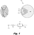
- Fig. 1 is a diagram of a neural lead (102) that has been implanted in proximity to target biological tissue (115).
- the neural lead (102) may be any of a number of different leads, including a cochlear lead, a brain stimulation lead, an optical prosthesis, a spinal cord stimulator, a muscle stimulator, a sensor, or other type of neural lead.
- the neural lead (102) includes an electrode (100) with an exposed surface (101) that makes electrical contact with the surrounding biological tissue.
- the electrode (100) is electrically connected to a signal wire (110) and supported by an implant body (105). Ideally, electrical signals pass down the signal wire (110) to the electrode (100) and from the electrode (100) to the target biological tissue (115).
- the electrode (100) is illustrated as being separated from the target biological tissue (115).
- the electrode (100) may be separated from the target auditory nerve endings by the cochlear fluid and a wall of a cochlear duct.
- the principles described below apply to electrodes that are in direct contact with the target tissue as well as configurations that have intervening fluids and/or tissue between the electrode and target tissue.
- a simplified electrical schematic of the interface between the electrode (100) and the target biological tissue (115) is shown below the cross sectional diagram.
- a first black circle on the right represents the electrode (100) and a second black circle on the left represents the target biological tissue (115).
- a first resistor R1 and a capacitor C1 represent the impedance at the surface of the electrode (100).
- the first resistance R1 and capacitance C1 can be dependent on a number of factors, including the exposed geometric surface area (GSA), the roughness of the electrode and the material that makes up the surface of electrode. For example, increasing the geometric size and/or active surface area of the electrode will increase its exposed surface area and its lower impedance.
- the electrical resistance of the biological environment between the electrode (100) and the target biological tissue (115) is shown by a second resistance R2.
- the second resistance R2 can be dependent on a number of factors including the concentrations of ions and proteins in fluids, the type of intervening tissues, and the distance between the electrode and the target tissue.
- the surface topology of the electrode can have significant effects on the performance of the system. For example, a rough electrode surface may have a greater active surface area in contact with biological tissues/fluids. This reduces the overall impedance at the electrode/tissue interface (R1 is significantly reduced while C1 is somewhat increased).
- electrode surfaces with very high aspect ratios may be prone to surface erosion. For example, peaks of the electrode surface may convey higher electrical currents to the surrounding tissues. These higher electrical currents may cause the peaks to dissolve into the biological tissue. This erosion can be undesirable for a number of reasons, including changes in the electrical characteristics of the electrode and contamination of the biological tissue.
- the surface topology may also influence the biological response of the body to the implant.
- the initial response to the surgical implantation of the electrode is nonspecific adsorption of the proteins to the surface of the implant.
- impedance of the interface increases, with a corresponding increase in power consumption of the implanted device.
- the surface topology, including the pore size, structure spacing/height, and morphology of the electrode surface can influence adhesion of fibroblasts and other connective tissue to the electrode surface.
- the surface topology of the electrode surface can be designed to reduce fibrous tissue formation and reduce surface impedance over the lifetime of the electrode.
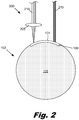
- Fig. 2 shows a cross sectional view of an implantable neural lead (102) that includes a body (105) and an electrode (100) with an exposed surface (101).
- the exposed surface (101) is in electrical contact with the surrounding biological tissues.
- the exposed surface (101) can be modified through application of laser energy.
- a focusing laser system (200) uses a lens (205) or other technique to focus the laser beam (210) onto the exposed surface (101) of the electrode (100).
- This technique may have a number of advantages, including a small spot/feature size and precise location.
- the exposed surface typically needs to be located at the focal point of the laser system, complex fixturing of both the laser and the electrode may be required.
- the use of a focusing laser system for modification of curved electrode surfaces can be even more challenging because the relative position and angle between the laser system and the electrode needs to be changed as the laser is scanned over the surface.
- Excimer lasers are a form of ultraviolet laser that uses noble gasses, including noble gas halides.
- the ultraviolet light from an excimer laser can add enough energy to disrupt the molecular bonds of a surface. This ablates the surface in a tightly controlled manner with almost no heating or change in the remainder of the material.
- the excimer laser can be used to produce localized melting rather than ablation.
- An excimer laser (215) does not typically have tight focusing requirements and can be effectively used at a range of distances to modify an electrode surface (101).
- An excimer laser (215) may be used to modify an electrode surface (101) that has topography variations on the range of 10 to 100 microns.
- a curved electrode surface (101) may have a center portion that is 50 microns higher than the edges of the electrode (100).
- the excimer laser (215) may be rastered across this surface without significant concern about the variation in height. If variations in the electrode surface (101) are greater than the tolerance of the excimer laser system, only coarse adjustments are necessary to bring it back into the acceptable range.
- Fig. 3 is a graph showing illustrative characteristics of an excimer laser (215, Fig. 2 ).
- the horizontal axis shows the duration of individual laser pulses in nanoseconds, with shorter pulses on the left and longer pulses on the right.
- the vertical axis shows intensity, in megawatts per centimeter square, with lower intensities on the bottom of the graph and higher intensities at the top of the graph.
- a third axis labeled ⁇ Tp is at an angle to the vertical axis and shows the surface temperatures generated for a given pulse length and intensity. The temperatures are given in degrees Celsius.
- a number of boxes have been drawn to show the various effects on surfaces the excimer laser is applied to.
- a shaded box labeled “Cleaning” is between 100 and 1,000 degrees Celsius with pulse durations of approximately one to hundreds of nanoseconds and intensities between approximately one and ten megawatts per centimeter square.
- a shaded box labeled “Melting” is between 1,000 and 10,000 degrees Celsius with pulse durations of approximately one nanosecond to hundreds of nanoseconds and intensities between approximately 1 and 100 megawatts per centimeter square.
- the portion labeled “Ablation” shows regions where the intensity and pulse durations produce localized temperatures exceeding 10,000 degrees.
- Fig. 4 shows one example of an illustrative method (400) for surface modification using an excimer laser (215).
- the lead (420) includes a recessed electrode (425) surrounded by an insulating body (430).
- the electrode (425) may be formed from platinum and joined to a silicone body (430).
- the electrode (425) may be placed in a mold and silicone may be injected around the electrode (425) and any wires or traces that are connected to the electrode (425).
- a layer of silicone (435) or other insulating material may be intentionally or unintentionally formed over the electrode (425).
- An excimer laser (215) may be used to remove all or a portion of the overlying silicone layer (435) (block 405).
- Flash Unintentional deposition of silicone over the electrode surface is called "flash.” Flash may be present in various thicknesses over electrode surfaces that were not completely seated against the mold. The parameters of the excimer laser system may be set to ablate the silicone flash with minimal disruption to the electrode surface itself.
- the conductive electrode surface may be intentionally covered with a thicker layer of silicone and an excimer laser (215) may be used to remove all or a portion of the silicone overlying the electrode surface.
- the removal of the overlying silicone layer (435) may result in particulates or other contaminants (440) being deposited on the electrode surface.
- the electrode surface (445) is cleaned to remove any contaminants from the previous operation (block 410).
- the electrode surface (445) may be cleaned using mechanical, chemical, or laser techniques.
- the lead (420) may be placed in an ultrasonic bath with a specific solution and temperature for a predetermined period of time.
- the electrode surface (445) may be cleaned through the application of additional laser energy.
- the electrode surface (445) may be mechanically cleaned.
- the electrode surface (445) is then modified to produce the desired surface texture (445') (block 415).
- an excimer laser (215) is used to ablate or melt the surface (445) of the electrode (425).
- Ablation of the electrode surface (445) is used to roughen the surfaces by producing high aspect ratio features. Appropriate selection of laser pulse length, laser intensity, and location of the laser on the electrode surface can produce the desired surface roughness.
- the high aspect ratio features may cover all or only a portion of the exposed surface.
- Fig. 5 shows one example where an additional electroplated coating is added to the electrode surface and then subsequently modified through application of laser energy.
- the electrode surface was electroplated using techniques that specifically increase the surface roughness.
- the electroplating material (500) may be the same or different than the underlying electrode material. The electroplating may be performed before the electrodes are encapsulated or after the electrode surface has been cleaned.
- the modified surface (505) has larger surface features and smoother profiles than the original electroplated material (500). This reduces the tendency of the peaks to dissolve.
- features with specific sizes and morphology can be formed. The sizes of the surface features can be selected to reduce adhesion of fibrous material to the electrode surface. As discussed above, adhesion of fibrous material to the electrode surface can increase the system impedance.
- the modification of the electrode surface using an excimer laser may be a two-step process.
- the excimer laser may be rastered over the electrode surface using high energy ablative settings to produce a high aspect ratio surface roughness.
- the high aspect surface roughness may cover all or only a portion of the exposed surface.
- the excimer laser may then be rastered over the electrode surface using lower energy settings to melt/consolidate peaks on the surface. This may create a porous structure.
- the melted/consolidated areas may cover all or only a portion of the high aspect ratio surface roughness.
- Fig. 6 shows an illustration of an electrode surface that has been selectively modified using an excimer laser.
- the excimer laser has been used to consolidate a high aspect ratio surface (600) to produce alternating stripes of high aspect ratio surface and laser consolidated surface (605).
- This change in surface roughness may serve a variety of purposes, including decreasing dissolution of electrode material and decreasing fibrous adhesion to the electrode surface.
- adding discontinuities in the electrode surface roughness may further reduce the impedance of the electrode. For example, the current density over the surface of the electrode increases at edges or other discontinuities. For a fixed electrode conductive area, an increase in the length of the edges or other discontinuities over the electrode surface can decrease impedance.
- an additional impedance reducing coating may be formed over the electrode surface.
- Figs. 7A, 7B, and 8 show various examples where an impedance reducing coating has been formed over the electrode surface.
- the impedance reducing coating may include platinum black, platinum gray, platinum/iridium alloys, dealloyed surfaces, conductive nanostructures or other materials.
- conductive polymers such as poly(3,4-ethylenedioxythiophene (PEDOT) could be used in an impedance reducing coating.
- PEDOT poly(3,4-ethylenedioxythiophene
- the impedance reducing coatings may be applied in a number of ways, including electrochemical deposition, electrostatic deposition, printing, manual application, or other technique.
- electrochemical deposition electrochemical deposition
- electrostatic deposition printing
- manual application or other technique.
- an ink containing platinum, iridium, or other conductive nanostructures may be printed onto the electrode surfaces using ink jet techniques.
- Fig. 7A shows an impedance reducing coating (700) disposed over the electrode (705).
- Fig. 7B shows the same impedance reducing coating (700) and electrode (705) with selected portions that have been modified using an excimer laser.
- the laser modified portions (710) have melted and combined the impedance reducing coating (700) and the underlying electrode material.
- the laser modified portions (710) may or may not cover the entire surface of the electrode (705).
- the impedance reducing coating (700) is more securely attached to the underlying electrode (705).
- the laser modified portions (710) may increase the surface area of the electrode (705) and decrease adhesion of fibrous tissue to the electrode surface.
- the impedance reducing coating (700) may be applied after the application of the laser energy.
- Fig. 8 shows one example of an electrode (800) with an excimer laser modified surface (805) and an impedance reducing overcoat (810).
- the impedance reducing coating (810) is formed on this excimer laser modified surface (805), the coating (810) can extend into these features to mechanically lock the coating (810) in place.
- the laser modification of the surface can be applied to the electrode surface itself or to a surface that is deposited over the electrode.
- the surface modification increases the electrochemical surface area of an electrode.
- the overcoat may have a charge transfer capability that is greater than that of the electrode surface.
- Surface modification of the electrode may also help impedance reducing coatings to more securely attach to the electrode.
- the modified surface may have feature sizes and distribution that inhibit adhesion and growth of biological tissues on the surface.
- the power consumption of the device can be significantly reduced.
- Lower power consumption and longer battery life will provide possibility for new system architectures such as fully implantable cochlear systems.
Description
- Neural prosthetics can be used for electrical stimulation of neural tissue and sensing neural signals in the central and peripheral nervous systems. These neural prosthetics include one or more electrodes that make electrical contact with neural tissue. The charge transfer characteristics of the electrodes define how efficiently the electrodes can transfer or receive electrical signals from the neural tissue.
US 2011/130815 A1 discloses a method for forming an implantable electrode by exposing a conductive surface of the implantable electrode with an application of an excimer laser, and creating a surface texture on a conductive surface by increasing the surface roughness by a surface ablation application of the excimer laser.
WO 2013/036988 A1 relates to an electrode for tissue stimulation, such as a cochlear electrode, wherein a recess is formed by an ablative method using an excimer laser in a carrier material, such a silicone, having a protective layer; the recess is of sufficient depth to allow the deposition of an electrode film.
US 2007/265691 A1 relates to an implantable paddle for spinal cord stimulation, wherein a Nd:YAG laser is used to create a set of traces by forming separating trenches in a metal layer; sufficient power is applied by the laser to ablate a small portion of the metal layer. An additional layer of nervous-tissue-compatible dielectric material is then added on top of the metal layer; the added layer is then patterned with a Nd:YAG or CO2 laser adapted for machining dielectric material to create a set of apertures.
US 5,800,500 relates to a cochlear implant electrode array, wherein each electrode comprises a small area of a particular wire where the dielectric materials have been removed by an UV laser beam which also seals the dielectric material to the wire by heating around the periphery of the electrode; the laser beam may be also used to heat the material surface to the point where it is roughened, thereby increasing the surface area and the current emitting capability of the electrode. - The accompanying drawings illustrate various embodiments of the principles described herein and are a part of the specification. The illustrated embodiments are merely examples and do not limit the scope of the claims.
-
Fig. 1 is a cross sectional diagram of an electrode and target tissue with a corresponding electrical schematic, according to one example of principles described herein. -
Fig. 2 is a diagram of laser modification of an electrode surface, according to one example of principles described herein. -
Fig. 3 is a graph of excimer laser performance for different pulse durations and intensities, according to one example of principles described herein. -
Fig. 4 is a flowchart of a method for surface modification of an electrode with corresponding illustrations, according to one example of principles described herein. -
Fig. 5 is a scanning electron microscope image of an electroplated surface that has been modified through application of excimer laser energy, according to one example of principles described herein. -
Fig. 6 is an illustration of an electrode surface modified through application of excimer laser energy to produce alternating texture stripes, according to one example of principles described herein. -
Fig. 7A is a cross sectional diagram of electrode with an impedance reducing coating, according to one example of principles described herein. -
Fig. 7B is a cross sectional diagram of an electrode with an impedance reducing coating that has been secured through application of excimer laser energy, according to one example of principles described herein. -
Fig. 8 is a cross sectional diagram of an electrode with laser modified surface and an impedance reducing overcoat deposited over the surface, according to one example of principles described herein. - Throughout the drawings, identical reference numbers designate similar, but not necessarily identical, elements.
- Neural prosthetics use electrodes to electrically stimulate neural tissue and sense electrical signals from the neural tissue. The charge transfer between the electrodes and neural tissue is in part determined by the electrochemistry of the electrode/tissue interface. To avoid energy losses and distortions of electrical signals, it can be advantageous for the electrical impedance of the interface to be small in the target stimulation/recording frequency range.
- Transfer of charge within the neural prosthetic device and its electrodes is carried out by the flow of electrons. Within the biological environment, however, transfer of charge is typically carried out by the flow of ionic current between two or more electrodes. Therefore, to mediate the transition from electron flow in the electrode to ion flow in the biological environment and to minimize the impedance of the interface, the material, size, shape and topography of the electrodes can be carefully selected.
The invention relates to a method as defined in claim 1. - In the following description, for purposes of explanation, numerous specific details are set forth in order to provide a thorough understanding of the present systems and methods. It will be apparent, however, to one skilled in the art that the present systems and methods may be practiced without these specific details. Reference in the specification to "an embodiment," "an example," or similar language means that a particular feature, structure, or characteristic described in connection with the embodiment or example is included in at least that one embodiment, but not necessarily in other embodiments. The various instances of the phrase "in one embodiment" or similar phrases in various places in the specification are not necessarily all referring to the same embodiment. Features shown and/or described in connection with one figure may be combined with features shown and/or described in connection with other figures.
- The absolute size and comparative sizes of objects illustrated in the figures is not necessarily to scale. The sizes of the objects have been illustrated to convey the principles described herein.
-
Fig. 1 is a diagram of a neural lead (102) that has been implanted in proximity to target biological tissue (115). The neural lead (102) may be any of a number of different leads, including a cochlear lead, a brain stimulation lead, an optical prosthesis, a spinal cord stimulator, a muscle stimulator, a sensor, or other type of neural lead. The neural lead (102) includes an electrode (100) with an exposed surface (101) that makes electrical contact with the surrounding biological tissue. The electrode (100) is electrically connected to a signal wire (110) and supported by an implant body (105). Ideally, electrical signals pass down the signal wire (110) to the electrode (100) and from the electrode (100) to the target biological tissue (115). For purposes of illustration, the electrode (100) is illustrated as being separated from the target biological tissue (115). For example, in a cochlear implant the electrode (100) may be separated from the target auditory nerve endings by the cochlear fluid and a wall of a cochlear duct. However, the principles described below apply to electrodes that are in direct contact with the target tissue as well as configurations that have intervening fluids and/or tissue between the electrode and target tissue. - A simplified electrical schematic of the interface between the electrode (100) and the target biological tissue (115) is shown below the cross sectional diagram. In the schematic, a first black circle on the right represents the electrode (100) and a second black circle on the left represents the target biological tissue (115). A first resistor R1 and a capacitor C1 represent the impedance at the surface of the electrode (100). The first resistance R1 and capacitance C1 can be dependent on a number of factors, including the exposed geometric surface area (GSA), the roughness of the electrode and the material that makes up the surface of electrode. For example, increasing the geometric size and/or active surface area of the electrode will increase its exposed surface area and its lower impedance.
- The electrical resistance of the biological environment between the electrode (100) and the target biological tissue (115) is shown by a second resistance R2. The second resistance R2 can be dependent on a number of factors including the concentrations of ions and proteins in fluids, the type of intervening tissues, and the distance between the electrode and the target tissue.
- The surface topology of the electrode can have significant effects on the performance of the system. For example, a rough electrode surface may have a greater active surface area in contact with biological tissues/fluids. This reduces the overall impedance at the electrode/tissue interface (R1 is significantly reduced while C1 is somewhat increased). However, electrode surfaces with very high aspect ratios may be prone to surface erosion. For example, peaks of the electrode surface may convey higher electrical currents to the surrounding tissues. These higher electrical currents may cause the peaks to dissolve into the biological tissue. This erosion can be undesirable for a number of reasons, including changes in the electrical characteristics of the electrode and contamination of the biological tissue.
- The surface topology may also influence the biological response of the body to the implant. The initial response to the surgical implantation of the electrode is nonspecific adsorption of the proteins to the surface of the implant. As a result of the growth of the fibrous layer, impedance of the interface increases, with a corresponding increase in power consumption of the implanted device. The surface topology, including the pore size, structure spacing/height, and morphology of the electrode surface can influence adhesion of fibroblasts and other connective tissue to the electrode surface. The surface topology of the electrode surface can be designed to reduce fibrous tissue formation and reduce surface impedance over the lifetime of the electrode.
-
Fig. 2 shows a cross sectional view of an implantable neural lead (102) that includes a body (105) and an electrode (100) with an exposed surface (101). The exposed surface (101) is in electrical contact with the surrounding biological tissues. The exposed surface (101) can be modified through application of laser energy. - On the left, a focusing laser system (200) is shown that uses a lens (205) or other technique to focus the laser beam (210) onto the exposed surface (101) of the electrode (100). This technique may have a number of advantages, including a small spot/feature size and precise location. However, because the exposed surface typically needs to be located at the focal point of the laser system, complex fixturing of both the laser and the electrode may be required. The use of a focusing laser system for modification of curved electrode surfaces can be even more challenging because the relative position and angle between the laser system and the electrode needs to be changed as the laser is scanned over the surface.
- Excimer lasers are a form of ultraviolet laser that uses noble gasses, including noble gas halides. In ablative applications, the ultraviolet light from an excimer laser can add enough energy to disrupt the molecular bonds of a surface. This ablates the surface in a tightly controlled manner with almost no heating or change in the remainder of the material. At lower energy levels/pulse durations, the excimer laser can be used to produce localized melting rather than ablation.
- An excimer laser (215) does not typically have tight focusing requirements and can be effectively used at a range of distances to modify an electrode surface (101). An excimer laser (215) may be used to modify an electrode surface (101) that has topography variations on the range of 10 to 100 microns. For example, a curved electrode surface (101) may have a center portion that is 50 microns higher than the edges of the electrode (100). The excimer laser (215) may be rastered across this surface without significant concern about the variation in height. If variations in the electrode surface (101) are greater than the tolerance of the excimer laser system, only coarse adjustments are necessary to bring it back into the acceptable range.
-
Fig. 3 is a graph showing illustrative characteristics of an excimer laser (215,Fig. 2 ). The horizontal axis shows the duration of individual laser pulses in nanoseconds, with shorter pulses on the left and longer pulses on the right. The vertical axis shows intensity, in megawatts per centimeter square, with lower intensities on the bottom of the graph and higher intensities at the top of the graph. A third axis labeled ΔTp is at an angle to the vertical axis and shows the surface temperatures generated for a given pulse length and intensity. The temperatures are given in degrees Celsius. A number of boxes have been drawn to show the various effects on surfaces the excimer laser is applied to. For example, a shaded box labeled "Cleaning" is between 100 and 1,000 degrees Celsius with pulse durations of approximately one to hundreds of nanoseconds and intensities between approximately one and ten megawatts per centimeter square. A shaded box labeled "Melting" is between 1,000 and 10,000 degrees Celsius with pulse durations of approximately one nanosecond to hundreds of nanoseconds and intensities between approximately 1 and 100 megawatts per centimeter square. The portion labeled "Ablation" shows regions where the intensity and pulse durations produce localized temperatures exceeding 10,000 degrees. -
Fig. 4 shows one example of an illustrative method (400) for surface modification using an excimer laser (215). In this implementation, the lead (420) includes a recessed electrode (425) surrounded by an insulating body (430). The electrode (425) may be formed from platinum and joined to a silicone body (430). The electrode (425) may be placed in a mold and silicone may be injected around the electrode (425) and any wires or traces that are connected to the electrode (425). A layer of silicone (435) or other insulating material may be intentionally or unintentionally formed over the electrode (425). An excimer laser (215) may be used to remove all or a portion of the overlying silicone layer (435) (block 405). Unintentional deposition of silicone over the electrode surface is called "flash." Flash may be present in various thicknesses over electrode surfaces that were not completely seated against the mold. The parameters of the excimer laser system may be set to ablate the silicone flash with minimal disruption to the electrode surface itself. - In other situations, the conductive electrode surface may be intentionally covered with a thicker layer of silicone and an excimer laser (215) may be used to remove all or a portion of the silicone overlying the electrode surface. The removal of the overlying silicone layer (435) may result in particulates or other contaminants (440) being deposited on the electrode surface.
- The electrode surface (445) is cleaned to remove any contaminants from the previous operation (block 410). For example, the electrode surface (445) may be cleaned using mechanical, chemical, or laser techniques. For example, the lead (420) may be placed in an ultrasonic bath with a specific solution and temperature for a predetermined period of time. In some examples, the electrode surface (445) may be cleaned through the application of additional laser energy. In other examples, the electrode surface (445) may be mechanically cleaned.
- The electrode surface (445) is then modified to produce the desired surface texture (445') (block 415). According to the invention, an excimer laser (215) is used to ablate or melt the surface (445) of the electrode (425). Ablation of the electrode surface (445) is used to roughen the surfaces by producing high aspect ratio features. Appropriate selection of laser pulse length, laser intensity, and location of the laser on the electrode surface can produce the desired surface roughness. The high aspect ratio features may cover all or only a portion of the exposed surface.
- The method described above is only one example. A variety of other configurations could be used. The steps described above could be reordered, combined, omitted, or additional steps could be added. In one example, additional coatings could be added.
Fig. 5 shows one example where an additional electroplated coating is added to the electrode surface and then subsequently modified through application of laser energy. According to the invention, the electrode surface was electroplated using techniques that specifically increase the surface roughness. The electroplating material (500) may be the same or different than the underlying electrode material. The electroplating may be performed before the electrodes are encapsulated or after the electrode surface has been cleaned. - Subsequent application of the excimer laser was used to melt and consolidate the peaks of the electroplated layer to form a modified surface (505). The modified surface (505) has larger surface features and smoother profiles than the original electroplated material (500). This reduces the tendency of the peaks to dissolve. Further, through selective application of the excimer laser, features with specific sizes and morphology can be formed. The sizes of the surface features can be selected to reduce adhesion of fibrous material to the electrode surface. As discussed above, adhesion of fibrous material to the electrode surface can increase the system impedance.
- In other examples, the modification of the electrode surface using an excimer laser may be a two-step process. The excimer laser may be rastered over the electrode surface using high energy ablative settings to produce a high aspect ratio surface roughness. The high aspect surface roughness may cover all or only a portion of the exposed surface.
- The excimer laser may then be rastered over the electrode surface using lower energy settings to melt/consolidate peaks on the surface. This may create a porous structure. The melted/consolidated areas may cover all or only a portion of the high aspect ratio surface roughness.
-
Fig. 6 shows an illustration of an electrode surface that has been selectively modified using an excimer laser. The excimer laser has been used to consolidate a high aspect ratio surface (600) to produce alternating stripes of high aspect ratio surface and laser consolidated surface (605). This change in surface roughness may serve a variety of purposes, including decreasing dissolution of electrode material and decreasing fibrous adhesion to the electrode surface. Additionally, adding discontinuities in the electrode surface roughness may further reduce the impedance of the electrode. For example, the current density over the surface of the electrode increases at edges or other discontinuities. For a fixed electrode conductive area, an increase in the length of the edges or other discontinuities over the electrode surface can decrease impedance. - In some examples, an additional impedance reducing coating may be formed over the electrode surface.
Figs. 7A, 7B, and 8 show various examples where an impedance reducing coating has been formed over the electrode surface. The impedance reducing coating may include platinum black, platinum gray, platinum/iridium alloys, dealloyed surfaces, conductive nanostructures or other materials. In one example, conductive polymers such as poly(3,4-ethylenedioxythiophene (PEDOT) could be used in an impedance reducing coating. These impedance reducing coatings can be applied before or after the application of the excimer laser energy to modify the electrode surface. For example, the impedance reducing coatings may be applied before the surface is modified. The impedance reducing coatings may be applied in a number of ways, including electrochemical deposition, electrostatic deposition, printing, manual application, or other technique. For example, an ink containing platinum, iridium, or other conductive nanostructures may be printed onto the electrode surfaces using ink jet techniques. - Application of the excimer laser energy may then be used to improve adhesion of the coating to the surface by partially melting portions of the electrode/impedance reducing coating.
Fig. 7A shows an impedance reducing coating (700) disposed over the electrode (705).Fig. 7B shows the same impedance reducing coating (700) and electrode (705) with selected portions that have been modified using an excimer laser. The laser modified portions (710) have melted and combined the impedance reducing coating (700) and the underlying electrode material. The laser modified portions (710) may or may not cover the entire surface of the electrode (705). By selectively applying laser energy, the impedance reducing coating (700) is more securely attached to the underlying electrode (705). Further, the laser modified portions (710) may increase the surface area of the electrode (705) and decrease adhesion of fibrous tissue to the electrode surface. - Additionally or alternatively, the impedance reducing coating (700) may be applied after the application of the laser energy.
Fig. 8 shows one example of an electrode (800) with an excimer laser modified surface (805) and an impedance reducing overcoat (810). For example, if a two-step laser process is used to create a high surface roughness and then consolidate the peaks, there may be significant overhangs, cavities and other features. When the impedance reducing coating (810) is formed on this excimer laser modified surface (805), the coating (810) can extend into these features to mechanically lock the coating (810) in place. - In sum, the new techniques and structures described above maximize the charge transfer of the electrode surface over the lifetime of an implant without significantly impacting the manufacturability of the electrode arrays. The laser modification of the surface can be applied to the electrode surface itself or to a surface that is deposited over the electrode. The surface modification increases the electrochemical surface area of an electrode. Where an impedance reducing overcoat is used, the overcoat may have a charge transfer capability that is greater than that of the electrode surface. Surface modification of the electrode may also help impedance reducing coatings to more securely attach to the electrode. Further, the modified surface may have feature sizes and distribution that inhibit adhesion and growth of biological tissues on the surface. By lowering the impedance at the surface of the electrode and ensuring that the impedance remains low throughout the lifetime of the implant, the power consumption of the device can be significantly reduced. Lower power consumption and longer battery life will provide possibility for new system architectures such as fully implantable cochlear systems.
- The preceding description has been presented only to illustrate and describe embodiments and examples of the principles described. This description is not intended to be exhaustive or to limit these principles to any precise form disclosed. Many modifications and variations are possible in light of the above teaching.
Claims (15)
- A method for forming an implantable electrode (100, 425, 705, 800) comprising:exposing a conductive surface (101, 445) of the implantable electrode with a first application of an excimer laser (215);creating a first surface texture on a conductive surface by increasing the surface roughness by a surface ablation application of the excimer laser or by forming an electroplated surface (500) over the conductive surface; andmodifying the first surface texture by melting and consolidating peaks of the first surface texture by subsequent application of the excimer laser to produce a second surface texture.
- The method of claim 1, wherein creating the first surface texture comprises rastering an excimer laser beam (215) over an electroplated coating (500) on the conductive surface (101, 445).
- The method of claim 1, wherein the first surface texture covers less than all of an exposed surface of the conductive surface (101, 445).
- The method of claim 1, wherein modifying the first surface texture to produce a second surface texture reduces sharp peaks to produce a second surface texture with reduced peak dissolution.
- The method of claim 4, wherein modifying the first surface texture to produce the second surface texture comprises rastering the excimer laser (215) over the first surface texture to restructure peaks of the first surface texture.
- The method of claim 1, wherein the second surface texture covers less than all of the first surface texture.
- The method of claim 1, further comprising disposing an impedance reducing coating (700, 810) over the conductive surface.
- The method of claim 7, wherein the impedance reducing coating (700, 810) comprises at least one of: platinum black, platinum gray, a platinum iridium alloy, activated iridium oxide, conductive nanostructures and conductive polymers.
- The method of claim 7, wherein disposing the impedance reducing coating (700, 810) over the conductive surface comprises printing platinum ink over the conductive surface.
- The method of claim 7, wherein the second surface texture has overhanging surface features and wherein the impedance reducing coating (700, 810) overlocks with the overhanging surface features.
- The method of claim 1, wherein the conductive surface (101, 445) comprises a first noble metal and the electroplated surface (500) comprise a second noble metal.
- The method of claim 11, wherein the first noble metal comprises platinum and the second noble metal comprises platinum.
- The method of claim 11, wherein creating the second surface texture on the conductive surface with the excimer laser (215) forms an alloy between the electroplated surface (500) and the conductive surface (101, 445).
- The method of claim 1, further comprising:folding a platinum sheet to form the conductive surface (101, 445); andliquid injection molding silicone (435) around the conductive surface.
- The method of claim 14, further comprising removing silicone flash (435) from the conductive surface (445) using a laser ablation process.
Applications Claiming Priority (1)
| Application Number | Priority Date | Filing Date | Title |
|---|---|---|---|
| PCT/US2013/055102 WO2015023280A1 (en) | 2013-08-15 | 2013-08-15 | Surface modified electrodes |
Publications (2)
| Publication Number | Publication Date |
|---|---|
| EP3033197A1 EP3033197A1 (en) | 2016-06-22 |
| EP3033197B1 true EP3033197B1 (en) | 2020-04-22 |
Family
ID=49004091
Family Applications (1)
| Application Number | Title | Priority Date | Filing Date |
|---|---|---|---|
| EP13751085.5A Active EP3033197B1 (en) | 2013-08-15 | 2013-08-15 | Method for forming an implantable electrode |
Country Status (3)
| Country | Link |
|---|---|
| US (1) | US10827936B2 (en) |
| EP (1) | EP3033197B1 (en) |
| WO (1) | WO2015023280A1 (en) |
Cited By (1)
| Publication number | Priority date | Publication date | Assignee | Title |
|---|---|---|---|---|
| DE102022202437A1 (en) | 2021-03-12 | 2022-09-15 | Heraeus Deutschland GmbH & Co. KG | Method of making an ablated conductor |
Families Citing this family (7)
| Publication number | Priority date | Publication date | Assignee | Title |
|---|---|---|---|---|
| EP3038702B1 (en) | 2013-08-27 | 2019-02-27 | Advanced Bionics AG | Thermoformed electrode arrays |
| EP3038701A1 (en) | 2013-08-27 | 2016-07-06 | Advanced Bionics AG | Asymmetric cochlear implant electrodes and method |
| EP3038703A1 (en) | 2013-08-27 | 2016-07-06 | Advanced Bionics AG | Implantable leads with flag extensions |
| US11097109B2 (en) | 2014-11-24 | 2021-08-24 | AtaCor Medical, Inc. | Cardiac pacing sensing and control |
| US20200194771A1 (en) * | 2018-12-12 | 2020-06-18 | NeuroTronik IP Holding (Jersey) Limited | Medical electrodes having enhanced charge capacities, and methods of manufacturing |
| US20200398044A1 (en) * | 2019-05-29 | 2020-12-24 | AtaCor Medical, Inc. | Implantable electrical leads and electrodes |
| CN116077829B (en) * | 2023-01-18 | 2023-12-15 | 微智医疗器械有限公司 | Implant device, electro-stimulator, and electrode plating method |
Family Cites Families (16)
| Publication number | Priority date | Publication date | Assignee | Title |
|---|---|---|---|---|
| US5473138A (en) * | 1993-07-13 | 1995-12-05 | Singh; Rajiv K. | Method for increasing the surface area of ceramics, metals and composites |
| US5683443A (en) * | 1995-02-07 | 1997-11-04 | Intermedics, Inc. | Implantable stimulation electrodes with non-native metal oxide coating mixtures |
| US5800500A (en) | 1995-08-18 | 1998-09-01 | Pi Medical Corporation | Cochlear implant with shape memory material and method for implanting the same |
| AU8681098A (en) * | 1997-08-01 | 1999-03-08 | Massachusetts Institute Of Technology | Three-dimensional polymer matrices |
| JP2001158813A (en) | 1999-10-27 | 2001-06-12 | Novartis Ag | Method for covering surface of material |
| US6869712B2 (en) * | 2002-03-07 | 2005-03-22 | Hewlett-Packard Development Company, L.P. | Ion exchange system structure with a microtextured surface, method of manufacture, and method of use thereof |
| US6974533B2 (en) * | 2002-04-11 | 2005-12-13 | Second Sight Medical Products, Inc. | Platinum electrode and method for manufacturing the same |
| US20050211680A1 (en) * | 2003-05-23 | 2005-09-29 | Mingwei Li | Systems and methods for laser texturing of surfaces of a substrate |
| US8099172B2 (en) | 2006-04-28 | 2012-01-17 | Advanced Neuromodulation Systems, Inc. | Spinal cord stimulation paddle lead and method of making the same |
| US8461042B2 (en) | 2009-12-01 | 2013-06-11 | Cochlear Limited | Electrode contact contaminate removal |
| US20110130815A1 (en) * | 2009-12-01 | 2011-06-02 | Peter Gibson | Contoured electrode contact surfaces |
| US8782884B2 (en) | 2009-12-01 | 2014-07-22 | Cochlear Limited | Manufacturing an electrode assembly having contoured electrode contact surfaces |
| EP2563464B1 (en) * | 2010-04-30 | 2018-06-06 | Second Sight Medical Products, Inc. | Improved biocompatible bonding method |
| AU2012308087A1 (en) | 2011-09-13 | 2014-03-06 | Hear Ip Pty Ltd | Biocompatible electrode component and method for fabrication thereof |
| JP2013074956A (en) | 2011-09-30 | 2013-04-25 | Nidek Co Ltd | Stimulus electrode for biological tissue and method of producing the stimulus electrode |
| US10791945B2 (en) * | 2013-05-30 | 2020-10-06 | Pulse Ip, Llc | Biocompatible implantable electrode |
-
2013
- 2013-08-15 WO PCT/US2013/055102 patent/WO2015023280A1/en active Application Filing
- 2013-08-15 US US14/907,409 patent/US10827936B2/en active Active
- 2013-08-15 EP EP13751085.5A patent/EP3033197B1/en active Active
Non-Patent Citations (1)
| Title |
|---|
| None * |
Cited By (1)
| Publication number | Priority date | Publication date | Assignee | Title |
|---|---|---|---|---|
| DE102022202437A1 (en) | 2021-03-12 | 2022-09-15 | Heraeus Deutschland GmbH & Co. KG | Method of making an ablated conductor |
Also Published As
| Publication number | Publication date |
|---|---|
| US10827936B2 (en) | 2020-11-10 |
| EP3033197A1 (en) | 2016-06-22 |
| US20160174860A1 (en) | 2016-06-23 |
| WO2015023280A1 (en) | 2015-02-19 |
Similar Documents
| Publication | Publication Date | Title |
|---|---|---|
| EP3033197B1 (en) | Method for forming an implantable electrode | |
| US5630839A (en) | Multi-electrode cochlear implant and method of manufacturing the same | |
| Schuettler et al. | Fabrication of implantable microelectrode arrays by laser cutting of silicone rubber and platinum foil | |
| US5800500A (en) | Cochlear implant with shape memory material and method for implanting the same | |
| US20100233226A1 (en) | Drug-eluting nanowire array | |
| US5524338A (en) | Method of making implantable microelectrode | |
| US20100305673A1 (en) | Ink Jet Printing of Implantable Electrodes | |
| AU2020202344B2 (en) | Biomedical electrode | |
| US20100036470A1 (en) | Laser-Based Fabrication of Implantable Stimulation Electrodes | |
| US8782884B2 (en) | Manufacturing an electrode assembly having contoured electrode contact surfaces | |
| JP2013074956A (en) | Stimulus electrode for biological tissue and method of producing the stimulus electrode | |
| AU2014202893B2 (en) | Biocompatible implantable electrode | |
| JP5313255B2 (en) | Optimal surface texture | |
| US20110130815A1 (en) | Contoured electrode contact surfaces | |
| EP2800589B1 (en) | Porous dealloyed electrodes | |
| CN1577656B (en) | Method for producing capacitor elements | |
| US20110127243A1 (en) | Electrode contact contaminate removal | |
| WO1996022864A1 (en) | Laser-machineable articles | |
| Kohler et al. | Parylene-coated metal tracks for neural electrode arrays-fabrication approaches and improvements utilizing different laser systems | |
| Corbett et al. | Polymer-based microelectrode arrays | |
| Yoo | Laser deinsulation of parylene-C coated Utah electrode array | |
| CN114602059A (en) | Electrode contact processing method and implantable electrode |
Legal Events
| Date | Code | Title | Description |
|---|---|---|---|
| PUAI | Public reference made under article 153(3) epc to a published international application that has entered the european phase |
Free format text: ORIGINAL CODE: 0009012 |
|
| 17P | Request for examination filed |
Effective date: 20160218 |
|
| AK | Designated contracting states |
Kind code of ref document: A1 Designated state(s): AL AT BE BG CH CY CZ DE DK EE ES FI FR GB GR HR HU IE IS IT LI LT LU LV MC MK MT NL NO PL PT RO RS SE SI SK SM TR |
|
| AX | Request for extension of the european patent |
Extension state: BA ME |
|
| DAX | Request for extension of the european patent (deleted) | ||
| GRAP | Despatch of communication of intention to grant a patent |
Free format text: ORIGINAL CODE: EPIDOSNIGR1 |
|
| STAA | Information on the status of an ep patent application or granted ep patent |
Free format text: STATUS: GRANT OF PATENT IS INTENDED |
|
| INTG | Intention to grant announced |
Effective date: 20191121 |
|
| GRAS | Grant fee paid |
Free format text: ORIGINAL CODE: EPIDOSNIGR3 |
|
| GRAA | (expected) grant |
Free format text: ORIGINAL CODE: 0009210 |
|
| STAA | Information on the status of an ep patent application or granted ep patent |
Free format text: STATUS: THE PATENT HAS BEEN GRANTED |
|
| AK | Designated contracting states |
Kind code of ref document: B1 Designated state(s): AL AT BE BG CH CY CZ DE DK EE ES FI FR GB GR HR HU IE IS IT LI LT LU LV MC MK MT NL NO PL PT RO RS SE SI SK SM TR |
|
| REG | Reference to a national code |
Ref country code: GB Ref legal event code: FG4D |
|
| REG | Reference to a national code |
Ref country code: CH Ref legal event code: EP |
|
| REG | Reference to a national code |
Ref country code: IE Ref legal event code: FG4D |
|
| REG | Reference to a national code |
Ref country code: DE Ref legal event code: R096 Ref document number: 602013068165 Country of ref document: DE |
|
| REG | Reference to a national code |
Ref country code: AT Ref legal event code: REF Ref document number: 1259435 Country of ref document: AT Kind code of ref document: T Effective date: 20200515 |
|
| REG | Reference to a national code |
Ref country code: LT Ref legal event code: MG4D |
|
| REG | Reference to a national code |
Ref country code: NL Ref legal event code: MP Effective date: 20200422 |
|
| PG25 | Lapsed in a contracting state [announced via postgrant information from national office to epo] |
Ref country code: NL Free format text: LAPSE BECAUSE OF FAILURE TO SUBMIT A TRANSLATION OF THE DESCRIPTION OR TO PAY THE FEE WITHIN THE PRESCRIBED TIME-LIMIT Effective date: 20200422 Ref country code: SE Free format text: LAPSE BECAUSE OF FAILURE TO SUBMIT A TRANSLATION OF THE DESCRIPTION OR TO PAY THE FEE WITHIN THE PRESCRIBED TIME-LIMIT Effective date: 20200422 Ref country code: LT Free format text: LAPSE BECAUSE OF FAILURE TO SUBMIT A TRANSLATION OF THE DESCRIPTION OR TO PAY THE FEE WITHIN THE PRESCRIBED TIME-LIMIT Effective date: 20200422 Ref country code: PT Free format text: LAPSE BECAUSE OF FAILURE TO SUBMIT A TRANSLATION OF THE DESCRIPTION OR TO PAY THE FEE WITHIN THE PRESCRIBED TIME-LIMIT Effective date: 20200824 Ref country code: IS Free format text: LAPSE BECAUSE OF FAILURE TO SUBMIT A TRANSLATION OF THE DESCRIPTION OR TO PAY THE FEE WITHIN THE PRESCRIBED TIME-LIMIT Effective date: 20200822 Ref country code: GR Free format text: LAPSE BECAUSE OF FAILURE TO SUBMIT A TRANSLATION OF THE DESCRIPTION OR TO PAY THE FEE WITHIN THE PRESCRIBED TIME-LIMIT Effective date: 20200723 Ref country code: NO Free format text: LAPSE BECAUSE OF FAILURE TO SUBMIT A TRANSLATION OF THE DESCRIPTION OR TO PAY THE FEE WITHIN THE PRESCRIBED TIME-LIMIT Effective date: 20200722 Ref country code: FI Free format text: LAPSE BECAUSE OF FAILURE TO SUBMIT A TRANSLATION OF THE DESCRIPTION OR TO PAY THE FEE WITHIN THE PRESCRIBED TIME-LIMIT Effective date: 20200422 |
|
| REG | Reference to a national code |
Ref country code: AT Ref legal event code: MK05 Ref document number: 1259435 Country of ref document: AT Kind code of ref document: T Effective date: 20200422 |
|
| PG25 | Lapsed in a contracting state [announced via postgrant information from national office to epo] |
Ref country code: BG Free format text: LAPSE BECAUSE OF FAILURE TO SUBMIT A TRANSLATION OF THE DESCRIPTION OR TO PAY THE FEE WITHIN THE PRESCRIBED TIME-LIMIT Effective date: 20200722 Ref country code: RS Free format text: LAPSE BECAUSE OF FAILURE TO SUBMIT A TRANSLATION OF THE DESCRIPTION OR TO PAY THE FEE WITHIN THE PRESCRIBED TIME-LIMIT Effective date: 20200422 Ref country code: HR Free format text: LAPSE BECAUSE OF FAILURE TO SUBMIT A TRANSLATION OF THE DESCRIPTION OR TO PAY THE FEE WITHIN THE PRESCRIBED TIME-LIMIT Effective date: 20200422 Ref country code: LV Free format text: LAPSE BECAUSE OF FAILURE TO SUBMIT A TRANSLATION OF THE DESCRIPTION OR TO PAY THE FEE WITHIN THE PRESCRIBED TIME-LIMIT Effective date: 20200422 |
|
| PG25 | Lapsed in a contracting state [announced via postgrant information from national office to epo] |
Ref country code: AL Free format text: LAPSE BECAUSE OF FAILURE TO SUBMIT A TRANSLATION OF THE DESCRIPTION OR TO PAY THE FEE WITHIN THE PRESCRIBED TIME-LIMIT Effective date: 20200422 |
|
| REG | Reference to a national code |
Ref country code: DE Ref legal event code: R097 Ref document number: 602013068165 Country of ref document: DE |
|
| PG25 | Lapsed in a contracting state [announced via postgrant information from national office to epo] |
Ref country code: EE Free format text: LAPSE BECAUSE OF FAILURE TO SUBMIT A TRANSLATION OF THE DESCRIPTION OR TO PAY THE FEE WITHIN THE PRESCRIBED TIME-LIMIT Effective date: 20200422 Ref country code: SM Free format text: LAPSE BECAUSE OF FAILURE TO SUBMIT A TRANSLATION OF THE DESCRIPTION OR TO PAY THE FEE WITHIN THE PRESCRIBED TIME-LIMIT Effective date: 20200422 Ref country code: IT Free format text: LAPSE BECAUSE OF FAILURE TO SUBMIT A TRANSLATION OF THE DESCRIPTION OR TO PAY THE FEE WITHIN THE PRESCRIBED TIME-LIMIT Effective date: 20200422 Ref country code: AT Free format text: LAPSE BECAUSE OF FAILURE TO SUBMIT A TRANSLATION OF THE DESCRIPTION OR TO PAY THE FEE WITHIN THE PRESCRIBED TIME-LIMIT Effective date: 20200422 Ref country code: DK Free format text: LAPSE BECAUSE OF FAILURE TO SUBMIT A TRANSLATION OF THE DESCRIPTION OR TO PAY THE FEE WITHIN THE PRESCRIBED TIME-LIMIT Effective date: 20200422 Ref country code: CZ Free format text: LAPSE BECAUSE OF FAILURE TO SUBMIT A TRANSLATION OF THE DESCRIPTION OR TO PAY THE FEE WITHIN THE PRESCRIBED TIME-LIMIT Effective date: 20200422 Ref country code: RO Free format text: LAPSE BECAUSE OF FAILURE TO SUBMIT A TRANSLATION OF THE DESCRIPTION OR TO PAY THE FEE WITHIN THE PRESCRIBED TIME-LIMIT Effective date: 20200422 Ref country code: ES Free format text: LAPSE BECAUSE OF FAILURE TO SUBMIT A TRANSLATION OF THE DESCRIPTION OR TO PAY THE FEE WITHIN THE PRESCRIBED TIME-LIMIT Effective date: 20200422 |
|
| PG25 | Lapsed in a contracting state [announced via postgrant information from national office to epo] |
Ref country code: SK Free format text: LAPSE BECAUSE OF FAILURE TO SUBMIT A TRANSLATION OF THE DESCRIPTION OR TO PAY THE FEE WITHIN THE PRESCRIBED TIME-LIMIT Effective date: 20200422 Ref country code: PL Free format text: LAPSE BECAUSE OF FAILURE TO SUBMIT A TRANSLATION OF THE DESCRIPTION OR TO PAY THE FEE WITHIN THE PRESCRIBED TIME-LIMIT Effective date: 20200422 |
|
| PLBE | No opposition filed within time limit |
Free format text: ORIGINAL CODE: 0009261 |
|
| STAA | Information on the status of an ep patent application or granted ep patent |
Free format text: STATUS: NO OPPOSITION FILED WITHIN TIME LIMIT |
|
| 26N | No opposition filed |
Effective date: 20210125 |
|
| PG25 | Lapsed in a contracting state [announced via postgrant information from national office to epo] |
Ref country code: MC Free format text: LAPSE BECAUSE OF FAILURE TO SUBMIT A TRANSLATION OF THE DESCRIPTION OR TO PAY THE FEE WITHIN THE PRESCRIBED TIME-LIMIT Effective date: 20200422 |
|
| REG | Reference to a national code |
Ref country code: CH Ref legal event code: PL |
|
| PG25 | Lapsed in a contracting state [announced via postgrant information from national office to epo] |
Ref country code: LU Free format text: LAPSE BECAUSE OF NON-PAYMENT OF DUE FEES Effective date: 20200815 Ref country code: CH Free format text: LAPSE BECAUSE OF NON-PAYMENT OF DUE FEES Effective date: 20200831 Ref country code: LI Free format text: LAPSE BECAUSE OF NON-PAYMENT OF DUE FEES Effective date: 20200831 |
|
| REG | Reference to a national code |
Ref country code: BE Ref legal event code: MM Effective date: 20200831 |
|
| PG25 | Lapsed in a contracting state [announced via postgrant information from national office to epo] |
Ref country code: SI Free format text: LAPSE BECAUSE OF FAILURE TO SUBMIT A TRANSLATION OF THE DESCRIPTION OR TO PAY THE FEE WITHIN THE PRESCRIBED TIME-LIMIT Effective date: 20200422 |
|
| PG25 | Lapsed in a contracting state [announced via postgrant information from national office to epo] |
Ref country code: FR Free format text: LAPSE BECAUSE OF NON-PAYMENT OF DUE FEES Effective date: 20200831 |
|
| PG25 | Lapsed in a contracting state [announced via postgrant information from national office to epo] |
Ref country code: IE Free format text: LAPSE BECAUSE OF NON-PAYMENT OF DUE FEES Effective date: 20200815 Ref country code: BE Free format text: LAPSE BECAUSE OF NON-PAYMENT OF DUE FEES Effective date: 20200831 |
|
| PG25 | Lapsed in a contracting state [announced via postgrant information from national office to epo] |
Ref country code: TR Free format text: LAPSE BECAUSE OF FAILURE TO SUBMIT A TRANSLATION OF THE DESCRIPTION OR TO PAY THE FEE WITHIN THE PRESCRIBED TIME-LIMIT Effective date: 20200422 Ref country code: MT Free format text: LAPSE BECAUSE OF FAILURE TO SUBMIT A TRANSLATION OF THE DESCRIPTION OR TO PAY THE FEE WITHIN THE PRESCRIBED TIME-LIMIT Effective date: 20200422 Ref country code: CY Free format text: LAPSE BECAUSE OF FAILURE TO SUBMIT A TRANSLATION OF THE DESCRIPTION OR TO PAY THE FEE WITHIN THE PRESCRIBED TIME-LIMIT Effective date: 20200422 |
|
| PG25 | Lapsed in a contracting state [announced via postgrant information from national office to epo] |
Ref country code: MK Free format text: LAPSE BECAUSE OF FAILURE TO SUBMIT A TRANSLATION OF THE DESCRIPTION OR TO PAY THE FEE WITHIN THE PRESCRIBED TIME-LIMIT Effective date: 20200422 |
|
| PGFP | Annual fee paid to national office [announced via postgrant information from national office to epo] |
Ref country code: GB Payment date: 20230828 Year of fee payment: 11 |
|
| PGFP | Annual fee paid to national office [announced via postgrant information from national office to epo] |
Ref country code: DE Payment date: 20230829 Year of fee payment: 11 |