EP3030874B1 - Montageanordnung für eine piezoelektrische sensorvorrichtung, - Google Patents
Montageanordnung für eine piezoelektrische sensorvorrichtung, Download PDFInfo
- Publication number
- EP3030874B1 EP3030874B1 EP14789871.2A EP14789871A EP3030874B1 EP 3030874 B1 EP3030874 B1 EP 3030874B1 EP 14789871 A EP14789871 A EP 14789871A EP 3030874 B1 EP3030874 B1 EP 3030874B1
- Authority
- EP
- European Patent Office
- Prior art keywords
- piezoelectric sensor
- piezoelectric
- opening
- sensor device
- installation according
- Prior art date
- Legal status (The legal status is an assumption and is not a legal conclusion. Google has not performed a legal analysis and makes no representation as to the accuracy of the status listed.)
- Active
Links
Images


Classifications
-
- H—ELECTRICITY
- H03—ELECTRONIC CIRCUITRY
- H03K—PULSE TECHNIQUE
- H03K17/00—Electronic switching or gating, i.e. not by contact-making and –breaking
- H03K17/94—Electronic switching or gating, i.e. not by contact-making and –breaking characterised by the way in which the control signals are generated
- H03K17/96—Touch switches
- H03K17/964—Piezoelectric touch switches
-
- G—PHYSICS
- G01—MEASURING; TESTING
- G01L—MEASURING FORCE, STRESS, TORQUE, WORK, MECHANICAL POWER, MECHANICAL EFFICIENCY, OR FLUID PRESSURE
- G01L1/00—Measuring force or stress, in general
- G01L1/16—Measuring force or stress, in general using properties of piezoelectric devices
-
- G—PHYSICS
- G01—MEASURING; TESTING
- G01L—MEASURING FORCE, STRESS, TORQUE, WORK, MECHANICAL POWER, MECHANICAL EFFICIENCY, OR FLUID PRESSURE
- G01L5/00—Apparatus for, or methods of, measuring force, work, mechanical power, or torque, specially adapted for specific purposes
- G01L5/22—Apparatus for, or methods of, measuring force, work, mechanical power, or torque, specially adapted for specific purposes for measuring the force applied to control members, e.g. control members of vehicles, triggers
- G01L5/226—Apparatus for, or methods of, measuring force, work, mechanical power, or torque, specially adapted for specific purposes for measuring the force applied to control members, e.g. control members of vehicles, triggers to manipulators, e.g. the force due to gripping
- G01L5/228—Apparatus for, or methods of, measuring force, work, mechanical power, or torque, specially adapted for specific purposes for measuring the force applied to control members, e.g. control members of vehicles, triggers to manipulators, e.g. the force due to gripping using tactile array force sensors
-
- H—ELECTRICITY
- H03—ELECTRONIC CIRCUITRY
- H03K—PULSE TECHNIQUE
- H03K2217/00—Indexing scheme related to electronic switching or gating, i.e. not by contact-making or -breaking covered by H03K17/00
- H03K2217/94—Indexing scheme related to electronic switching or gating, i.e. not by contact-making or -breaking covered by H03K17/00 characterised by the way in which the control signal is generated
- H03K2217/96—Touch switches
- H03K2217/96015—Constructional details for touch switches
Definitions
- the invention relates to piezoelectric input sensors and to apparatuses and installations in which such piezoelectric sensors are used.
- a piezoelectric sensor is a device that uses the piezoelectric effect to measure pressure, acceleration, strain or force by converting them to an electrical charge.
- a piezoelectric sensor that can be used to measure pressure, force or strain under a surface (overlay) is known from published patent application WO 2011/158 154 A2 (hereinafter the '154 patent), for example.
- the piezoelectric sensor comprises a layer of piezoelectric material sandwiched between a PCB and an electrically conductive foil.
- the electrically conductive foil is attached to the overlay by means of an adhesive layer.
- the piezoelectric touch switch of the kind described in the '154 patent is widely used in different kinds of apparatuses and installations.
- the overlays used in apparatuses and installations can be selected from a very large group of materials and qualities, each having different physical properties.
- the thickness of the overlay and the material, of which the overlay has been made, for example, can be different for each kind of apparatus or installation.
- the elasticity of the overlay i.e. how much the overlay bends if a given force or pressure is exerted on it
- the thickness or elasticity may depend on the position where the piezoelectric sensor switch is assembled, for example, structures show a smaller elasticity close to corners. A displacement of a few millimetres can influence the elasticity or stiffness significantly, in particular if the displacement is towards a stabilizing structure such as a ridge or corner (or further therefrom).
- the piezoelectric sensor is a piezoelectric touch switch
- tuning is normally required in order to have the switching threshold defined.
- the aim of the matching is to have the switch not to switch too early (to avoid registering noise as switching, i.e. avoiding false alarms) and to have the switch to switch when a high enough pressure, force or strain is exerted on the overlay (to enable registering a reasonable pressure, force or strain as a valid switching command).
- the simplification may be seen in a reduction of the need for matching of the piezoelectric sensor on electronics level or on software level. This objective can be fulfilled with the apparatus or installation according to claim 1.
- the apparatus or installation comprises a surface and at least one piezoelectric sensor device that is a piezoelectric touch switch comprising at least one piezoelectric sensor that comprises at least one sheet of piezoelectric material on a substrate supported by edges of an opening.
- the at least one piezoelectric sensor device is located below the surface so that the surface functions as overlay to the piezoelectric touch switch.
- the piezoelectric sensor device is configured so that the piezoelectric sensor bends into the opening in response to a force or pressure exerted on the surface causing the surface to bend.
- the apparatus or installation further comprises a piezoelectric sensor device mounting arrangement, by which the piezoelectric sensor device has been assembled and which comprises a mounting bracket defining at least one opening.
- the mounting bracket has been attached to the surface from below with attaching means by adhesion, the at least one piezoelectric sensor being located in the area of the opening.
- the mounting arrangement comprises at least one backer piece connected to the mounting bracket, at least one squeezer in the area of the opening between the at least one backer piece and the at least one piezoelectric sensor, and at least one sensitivity booster in the area of the opening between the surface and the at least one piezoelectric sensor.
- the backer piece is connected to the mounting bracket by continuously adjustable compression adjusting means that operate on the backer piece to compress the sensitivity booster, the piezoelectric sensor device and the at least one squeezer between the overlay and the backer piece without penetrating the surface, for compensating the surface tolerances or mounting tolerances, and with which the compression of the squeezer, the piezoelectric sensor device and the sensitivity booster is adjustable.
- the components of the mounting arrangement have been configured in such a manner that, when the mounting bracket is attached to the surface with the attaching means and the components have been assembled, the piezoelectric sensor device and the at least one squeezer, and also the at least sensitivity booster will be compressed between the surface and the backer piece.
- a separate plate or other piece (such as grid or net) belonging to an assembly kit of the mounting arrangement can be used, or, alternatively, a structure (in particular plate, grid or net or other piece) in the apparatus or installation can be used.
- the signal seen by electromechanical system (comprising piezoelectric sensor elements and required measurement electronics set-up) can be standardized to the level that ensures optimal signal processing for touch switch functionality in apparatuses and installations with a very large range of physical properties of the surface. Furthermore, a wide range of operational conditions can be achieved since the mounting arrangement is mechanically stable and may show a high temperature stability. This simplifies significantly the work that is necessary to match the piezoelectric sensor device to each apparatus or installation.
- An advantage of the mounting arrangement is that the piezoelectric sensor can be integrated at a later stage of product assembly than the configuration disclosed in the '154 patent. This reduces the failure risks due to the product assembly, and improves the freedom of design to locate the piezoelectric sensor device at several places of the end product.
- the area of piezoelectric sensor may be smaller or larger than the defined key area which typically is 10 to 20 mm in diameter.
- the piezoelectric sensor should be triggerable with by initial force levels of 0.1N to 10N exerted by the user on the surface at the defined key area.
- the force necessary as a valid key input can be adjusted electronically, as defined in our (at the time of writing unpublished) European patent application 13155986.6 .
- the sensitivity value for each piezoelectric sensor may be set by a remote device via communication protocol to control microcontroller in which threshold values have been stored.
- the triggering force for the key area should preferably be more than 2-10 times larger than the non-active area of the touch switch (outside the defined button area).
- the apparatus or installation may further comprise at least one sensitivity booster in the area of the opening between the surface and the at least one piezoelectric sensor.
- the improvement may further comprise the step of using a sensitivity booster to improve a force, pressure, or strain transferring contact between the surface and the piezoelectric sensor, and optionally also to mechanically reduce cross-talk between the piezoelectric sensors. This improves the reliability of the piezoelectric sensor device against false alarms.
- the sensitivity of the piezoelectric touch switch can be improved. If the apparatus or installation has a surface manufacturing tolerance of approximately 100 ⁇ m, it may be possible to detect a rather small bending of the surface, such as when the surface bends inwards approximately 1 ⁇ m, or, more generally, inwards approximately 1 to 10 ⁇ m.
- the shape of the sensitivity booster may be configured to mechanically lead to a force, pressure or strain-induced deformation of the overlay at the location surrounding a piezoelectric sensor to the piezoelectric sensor. This may increase the reliability of the piezoelectric sensor even with thick or stiff surfaces.
- the sensitivity booster may comprise at least one region with locally increased thickness, such as a hill, a leg or a ridge, at the location of at least one piezoelectric sensor.
- the sensitivity booster may be a separate piece or it may be integrated in the surface (in particular, if the sensitivity booster is implemented as or comprising at least one area in the surface with bridges or sections milled out).
- the shape of the sensitivity booster may have been configured to mechanically prevent a force, pressure or strain-induced deformation of the surface at the location of a piezoelectric sensor from propagating to a neighboring piezoelectric sensor. This improves the reliability of the piezoelectric sensor against false alarms. Therefore, the sensitivity booster may comprise a region with reduced thickness, such as a valley or a recess, at a location around the at least one hill, leg or ridge. Alternatively or in addition, the sensitivity booster may be designed to block forces from outside a user interface area to propagate towards any piezoelectric sensor, preferably by having hills, legs or ridges around the area of the piezoelectric sensor or sensors.
- the at least one squeezer may have at least one opening, that in particular may be a recession, to reduce back-coupling of the forces to the piezoelectric sensor and/or to facilitate the bending of the piezoelectric sensor.
- the opening may be located below the respective piezoelectric sensor, or laterally displaced from the piezoelectric sensor. If the opening is laterally displaced from the piezoelectric sensor, the piezoelectric sensor may be bent with a smaller force even if the piezoelectric sensor has been assembled on a supporting structure, in particular on a printed circuit board.
- the squeezer will compress the piezoelectric sensor device against the surface (or against the optional at least one sensitivity booster which in turn is being compressed against the surface) and reduce the possibility of the piezoelectric sensor device losing contact with the surface.
- This enables using the piezoelectric sensor device in apparatuses or installations in high temperatures.
- the compression of the piezoelectric sensor device and the at least one squeezer and optionally also the at least one sensitivity booster will remain or even increase if the temperature rises, preferably at least in the preferred temperature range from 20 °C to ca. 80-85 °C.
- the attaching means may be or comprise adhesive on top of the mounting bracket.
- the mounting bracket may be connected to the surface by adhesive, and the sensitivity booster and/or the at least one squeezer are configured to compensate for stiffness or elasticity of the overlay, for geometrical hysteresis, such as due to heat cycling, or for geometrical inaccuracies, such as due to manufacturing tolerances, in such a manner that a reference force, pressure or strain exerted to the overlay generates an output of the at least piezoelectric sensor that is within a pre-defined range, by setting the continuously adjustable compression adjusting means to a defined position.
- the expected magnitude of signal received at the microcontroller in response to user feedback can therefore have a pre-defined magnitude range, enabling fine-tuning if required, by the manufacturer of the apparatus or the installation, by a remote host using a communication connection or a signalling line, or even automatically.
- the attaching means adhere to the surface from below in such a manner that the opposite side of the surface remains intact. In this manner, the surface does not need to be pierced, in contrast to the situation that as attaching means screws or bolts are used that need to penetrate through the surface.
- the surface is a uniform surface.
- the attaching means adhere to the surface from below in such a manner that the opposing side of the surface remains intact, since in this case the surface does not necessarily be treated at all, except potentially polishing, brushing, varnishing and/or lacquering.
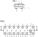
- FIG 1 illustrates a cut through surface 2 of apparatus 1 or installation, under which the piezoelectric sensor device mounting arrangement has been attached.
- FIG 2 illustrates the piezoelectric sensor device mounting arrangement as seen from below.
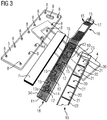
- FIG 3 is an exploded view of components of a first configuration of the piezoelectric sensor device mounting arrangement shown in FIG 1 and 2 .
- Piezoelectric sensor device mounting arrangement comprises a mounting bracket 4 defining an opening 10, adhesive 3 on top of the mounting bracket 4 for attaching the bracket to the surface 2 (as overlay to the piezoelectric sensors), and at least one backer piece 5.
- the piezoelectric sensor device mounting arrangement comprises a piezoelectric sensor device, such as a switch array 18, that comprises at least one piezoelectric sensor 13 (such as a sheet 13a of piezoelectric material on substrate 14) that is placeable or located in the area of the opening 10.
- a piezoelectric sensor device such as a switch array 18, that comprises at least one piezoelectric sensor 13 (such as a sheet 13a of piezoelectric material on substrate 14) that is placeable or located in the area of the opening 10.
- the piezoelectric sensor device mounting arrangement may further comprise at least one sensitivity booster 19 that is placeable or located in the area of the opening 10.
- the piezoelectric sensor device mounting arrangement further comprises at least one squeezer 7 that is placeable or located in the area of the opening 10.
- the squeezer 7 is shown bottom up in FIG 3 .
- sensitivity booster 19 is made of or comprises aluminium, steel or acrylate. Even though sensitivity booster 19 has been shown as a separate part, it can be an integral part of the surface 2.
- the sensitivity booster 19 can be produced by moulding or milling, for example.
- squeezer 7 is made of or comprises rubbery-elastic material, such as rubber.
- Squeezer 7 can have the shape of a slab (or segments of a slab) or a cushion. Instead of one squeezer 7, there may be a plurality of squeezers 7.
- the squeezer 7 (or squeezers 7) may be attached to piezoelectric sensor device from below.
- the components of the piezoelectric sensor device mounting arrangement have been configured in such a manner that, when the mounting bracket 4 is attached to the surface 2 with the adhesive 3, the sensitivity booster 19, the piezoelectric sensor device (the switch array 18) and the at least one squeezer 7 will be compressed between the surface 2 and the backer piece 5.
- Mounting bracket 4 is adhered to surface 2 by adhesive 3. After this, sensitivity booster 19 is placed in opening 10 against the surface 2, after which the piezoelectric sensor device is put in place. Then squeezer 7 is placed below the piezoelectric sensor device. The structure is closed by backer piece 5 which is fastened with screws 6, for example, via openings 10 in the backer piece.
- the tightness of the piezoelectric sensor device mounting arrangement i.e. the compression of the squeezer 7, the piezoelectric sensor device and the sensitivity booster 19 can conveniently be adjusted by adjusting the tightness of the screws 6.
- any other, however preferably adjustable, fastening means can be used.
- the mounting arrangement can be opened for replacing the piezoelectric sensor without replacing the surface 2. Because of the adhesive 3, it would be difficult to remove the mounting bracket 4 from the surface 2. If there would be failure of piezoelectric sensor, it would be enough to open the mounting arrangement and replace the piezoelectric sensor, and then close the mounting arrangement.
- FIG 3 shows an exemplary embodiment of the piezoelectric sensor device in which switch array 18 is implemented with sheets 13a of piezoelectric material on substrate 14, with dot 12 on top of each sheet 13a piezoelectric material.
- switch array 18 On top of switch array 18 is a conductive foil 11.
- the substrates 14 are connected to common ground 34 of flat cable 16.
- Each sheet 13a of piezoelectric material is connected to dedicated conductor 15 of flat cable 16 and can so therefore be read from flat cable connector 17.
- the flat cable connector 17 and the respective end of the flat cable 16 are preferably placed outside of the piezoelectric sensor device mounting arrangement.
- the backer piece 5 may have a suitable opening 9.
- sensitivity booster 19 can be implemented as slab that comprises elevated booster regions such as hills 20. Next to the elevated regions, deeper regions such as valleys 21 are preferably present. Edges of sensitivity booster 19 may be configured as ridges 22. Similarly, ridges 22 may separate neighbour valleys 21 from each other. End zone 23 of sensitivity booster 23 is preferably wider than the ridges 22.
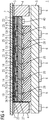
- FIG 4 illustrates section at IV-IV of a second configuration of the piezoelectric sensor mounting arrangement shown in FIG 2 , namely, another exemplary embodiment of the piezoelectric sensor device that is a printed circuit board 27 (PCB) based piezoelectric sensor device instead of a switch array 18 -based piezoelectric sensor device, the parts of which were illustrated in FIG 3 .
- PCB printed circuit board 27
- the PCB 27 can be a flexible PCB or a conductive foil.
- Microcontroller 40 can be a separate integrated circuit, a programmable gate array (PGA), a synthetized or integrated microcontroller core in a programmable gate array, a custom application specific integrated circuit (ASIC), or any other device that can execute a program.
- PGA programmable gate array
- ASIC application specific integrated circuit
- FIG 8 Below in the context of FIG 8 an exemplary electronic circuit 90 for operating a piezoelectric sensor device is disclosed in more detail.
- the electronic circuit 90 is most conveniently implemented on PCB 27.
- the piezoelectric sensors 13 comprise sheets 13a of piezoelectric material placed on substrate 14. Each of the substrates 14 is supported by edges of opening 28 (cf. FIG 5 ) in PCB 27. This enables the bending of the piezoelectric sensor 13.
- the sheets 13a of piezoelectric material are covered by conductive foil 11 which is attached to PCB 27 by adhesive 25.
- the conductive foil 11 acts as common ground.
- the substrates 14 are connected to PCB contacts 26 and so to electronic circuit 90.
- FIG 5 illustrates propagation of force from a force distribution F exerted of surface 2 of the apparatus 1 or installation at the location shown which is closer to the mounting bracket 4 than to the piezoelectric sensors 13.
- a force distribution F exerted of surface 2 of the apparatus 1 or installation at the location shown which is closer to the mounting bracket 4 than to the piezoelectric sensors 13.
- most of the force distribution F propagates along the surface, through adhesive 3 and mounting bracket 4, or via the sensitivity booster 1, PCB 27 and squeezer 7 to backer piece 5. Only a fraction of the force distribution F passes to the piezoelectric sensor 13.
- the piezoelectric sensor device mounting arrangement can be seen to act as a barrier to avoid registering noise at the piezoelectric sensors 13 as switching. This helps avoiding false alarms.
- the mounting arrangement is particularly effective against noise resulting from force distributions outside of the mounting bracket 4. However, the mounting arrangement is still effective also against noise resulting force distributions closer to the mounting bracket 4 than the piezoelectric sensors 13.
- the squeezer 7 may therefore have one or more openings 30 (i.e. recessions) located around the sheets 13a of piezoelectric material and hills 29 (such as, for example, legs or the normal height) at the location of the sheets 13a of piezoelectric material.
- Each opening 30 may be located below the respective piezoelectric sensor 13, and/or laterally displaced from the respective piezoelectric sensor 13.
- sensitivity booster 19 A further effect of sensitivity booster 19 is that it together with mounting bracket 4 blocks propagation of forces from outside the user interface area that could disturb any one of the piezoelectric sensor elements. Also the squeezer 7 attenuates the propagation of such forces.
- force distribution F in FIG 5 falls in mechanical noise blocking area 31 defined by the piezoelectric sensor device mounting arrangement.
- Mechanical blocking areas 31 are preferably situated at ends of the PCB 27 or switch array 18.
- mechanical noise blocking areas 32 between each piezoelectric sensor 13.
- Mechanical noise blocking areas 31, 32 can also be seen as a means for mechanically reducing cross-talk (or noise, as explained above) between the piezoelectric sensors 13.
- FIG 7 The configuration of mechanically reducing cross-talk between the piezoelectric sensors 13 is schematically illustrated in FIG 7 .
- the ridges 22 and end zone(s) 23 of the sensitivity booster 19 and the legs of the squeezer 7 reduce cross-talk.
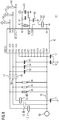
- FIG 8 is a simplified circuit showing certain components of electronic circuit 90 for a piezoelectric sensor device configuration with three piezoelectric sensors 13.
- the person skilled in the art understands that instead of using three piezoelectric sensors, any number of piezoelectric sensors 13 can be used. Most practically, the number of piezoelectric sensors 13 is 1, 2, 3, 4, 5, 6, ... to a few dozens.
- the piezoelectric sensors 13 are most preferably arranged in one-dimensional or two-dimensional arrays.
- First piezoelectric sensor element 13, I is connected through resistors 44, 47, 52 between the VREF and PZ1-ADC pins of microcontroller 40.
- Second piezoelectric sensor element 13, II is connected through resistors 45, 48, 52 between the VREF and PZ2-ADC pins of microcontroller 40.
- Third piezoelectric sensor element 13, III is connected through resistors 46, 49, 52 between the VREF and PZ3-ADC pins of microcontroller 40.
- PZ1-ADC, PZ2-ADC and PZ3-ADC pins lead to the first, second and third analog-to-digital-converter channels.
- the signal indicating voltage over first piezoelectric sensor element 13, I, second piezoelectric sensor element 13, II and third piezoelectric sensor element 13, III can be converted to digital signals and processed by microcontroller 40.
- boost converter (not shown in FIG 8 ; the realization of the boost converter has been disclosed in European patent application 13155986.6 , at the time of writing still unpublished).
- the purpose of boost converter is to raise the operating voltage across any of the piezoelectric sensors 13 (i.e. 13, I; 13, II; 13, III) up to 200 V (or to other suitably high voltage) to enable it to vibrate enough the surface 2 for tactile signalling.
- This is achieved via a typical boost (or "step-up") converter circuit, consisting of regular coil, FET, diode and capacitors, along with the switching cicrcuits to direct high voltages to one or multiple of piezo sensors 13 at a time, as controlled by the microcontroller 40.
- the operating voltage of the piezoelectric sensor 13 that detected the touch switching is raised.
- the tactile signalling is preferably used to indicate a valid touch switch interaction.
- valid a touch switch interaction is meant that fulfils preset criteria, such as, regarding duration and/or magnitude of the bending of the piezoelectric sensor 13, especially but not limited to exceed a respective lower limit.
- the buzzer 65 may be used for audibly indicating a valid touch switch interaction.
- leds or other suitable light sources such as lamps can be connected, most preferably through resistors 58, 59, 60, for indicating valid touch switch interaction.
- Each piezoelectric sensor 13 (such as 13, I; 13, II; and 13,111; or all five piezoelectric sensors 13 such as in the examples in FIG 1 - 4 ; or all piezoelectric sensors 13 of the piezoelectric sensor device) may be connected to common line VREF via conductive foil 11 from above and connected to printed circuit board 27 via dome 50. Connection from below is connected to corresponding ADC channel of microcontroller 40 (e.g. PZ1-ADC, PZ2-ADC, PZ3-ADC if three piezoelectric sensors 13,1 13,11 and 13,III are used) via PCB 27 routing through filtering circuitry (e.g. capacitors 51, 53, 54, 55, 56, 57 and resistors 44, 45, 46, 47, 48, 49, 52 in FIG 8 ).
- filtering circuitry e.g. capacitors 51, 53, 54, 55, 56, 57 and resistors 44, 45, 46, 47, 48, 49, 52 in FIG 8 ).
Landscapes
- Physics & Mathematics (AREA)
- General Physics & Mathematics (AREA)
- Chemical & Material Sciences (AREA)
- Analytical Chemistry (AREA)
- Force Measurement Appropriate To Specific Purposes (AREA)
- Electronic Switches (AREA)
Claims (12)
- Vorrichtung (1) oder Installation, umfassend:- eine Oberfläche (2); und- wenigstens eine piezoelektrische Sensorvorrichtung (18, 27, 90), die ein piezoelektrischer Berührungsschalter ist, der wenigstens einen piezoelektrischen Sensor (13) enthält, der wenigstens eine Lage (13a) aus piezoelektrischem Material auf einem Substrat (14), das von den Kanten einer Öffnung (28) getragen wird, aufweist, wobei sich der wenigstens eine piezoelektrische Sensor (13) unter der Oberfläche (2) befindet, so dass die Oberfläche (2) als Abdeckung für den piezoelektrischen Berührungsschalter dient, wobei die piezoelektrische Sensorvorrichtung (18, 27, 90) so konfiguriert ist, dass sich der piezoelektrische Sensor (13) in Reaktion auf eine Kraft oder einen Druck, die bzw. der auf die Oberfläche (2) ausgeübt wird und bewirkt, dass sich die Oberfläche (2) biegt, in die Öffnung (28) biegt,gekennzeichnet durch
eine Anordnung für die Montage der piezoelektrischen Sensorvorrichtung, durch die die piezoelektrische Sensorvorrichtung (18, 27, 90) zusammengefügt worden ist und die umfasst:- einen Montageträger (4), der wenigstens eine Öffnung (10) definiert, wobei der Montageträger (4) an der Oberfläche (2) von unten mit Befestigungsmitteln (3) durch Kleben befestigt ist, wobei sich der wenigstens eine piezoelektrische Sensor (13) in dem Bereich der Öffnung (10) befindet;- wenigstens ein Gegenstück (5), das mit dem Montageträger (4) durch stufenlos einstellbare Kompressionseinstellmittel (6) verbunden ist;- wenigstens eine Quetscheinrichtung (7) im Bereich der Öffnung (10) zwischen dem wenigstens einen Gegenstück (5) und dem wenigstens einen piezoelektrischen Sensor (13); und- wenigstens einen Empfindlichkeitsverstärker (19) im Bereich der Öffnung (10) zwischen der Oberfläche (2) und dem wenigstens einen piezoelektrischen Sensor (13);wobei die stufenlos einstellbaren Kompressionseinstellmittel (6) auf das Gegenstück (5) wirken, um den wenigstens einen Empfindlichkeitsverstärker (19), die piezoelektrische Sensorvorrichtung (18, 27, 90) und die wenigstens eine Quetscheinrichtung (7) zu komprimieren, ohne in die Oberfläche (2) einzudringen, um die Toleranzen der Oberfläche (2) oder die Montagetoleranzen auszugleichen, und mit denen die Kompression der Quetscheinrichtung (7), der piezoelektrischen Sensorvorrichtung (18, 27, 90) und des Empfindlichkeitsverstärkers (19) einstellbar ist. - Vorrichtung (1) oder Installation nach Anspruch 1,
wobei die wenigstens eine Quetscheinrichtung (7) wenigstens eine Öffnung (30) besitzt, die insbesondere eine Aussparung sein kann, um das Biegen des piezoelektrischen Sensors (13) zu erleichtern. - Vorrichtung (1) oder Installation nach Anspruch 2,
wobei sich die wenigstens eine Öffnung (30) unter dem piezoelektrischen Sensor (13) befindet. - Vorrichtung (1) oder Installation nach einem vorhergehenden Anspruch,
wobei sich die wenigstens eine Öffnung (30) seitlich versetzt zu dem piezoelektrischen Sensor (13) befindet. - Vorrichtung (1) oder Installation nach einem der vorhergehenden Ansprüche,
wobei die wenigstens eine Quetscheinrichtung (7) eine Wärmeausdehnung zeigt, die größer als die Wärmeausdehnung des Montageträgers (4) ist und vorzugsweise auch größer als die Wärmeausdehnung des Gegenstücks (5) ist. - Vorrichtung (1) oder Installation nach einem der vorhergehenden Ansprüche,
wobei die Befestigungsmittel (3) Klebstoff (3) auf der Oberseite des Montageträgers (4) sind oder umfassen. - Vorrichtung (1) oder Installation nach einem der vorhergehenden Ansprüche,
wobei der Montageträger (4) mit der Oberfläche (2) durch Klebstoff (3) verbunden ist und der Empfindlichkeitsverstärker (19) und/oder die wenigstens eine Quetscheinrichtung (7) konfiguriert sind, die Steifigkeit oder Elastizität des Überzugs (2), die geometrische Hysterese, die etwa durch eine zyklische Wärmeveränderung bedingt ist, oder geometrische Ungenauigkeiten, die etwa durch Herstellungstoleranzen bedingt sind, in der Weise auszugleichen, dass eine Referenzkraft, ein Referenzdruck oder eine Referenzdehnung, die bzw. der auf den Überzug (2) ausgeübt wird, eine Ausgabe des wenigstens einen piezoelektrischen Sensors (13) erzeugt, der innerhalb eines im Voraus definierten Bereichs liegt, indem die stufenlos einstellbaren Kompressionseinstellmittel (6) auf eine definierte Position eingestellt werden. - Vorrichtung (1) oder Installation nach einem der vorhergehenden Ansprüche, wobei
die Befestigungsmittel (3) an der Oberfläche (2) von unten in der Weise haften, dass die gegenüberliegende Seite der Oberfläche (2) intakt bleibt. - Vorrichtung (1) oder Installation nach einem der vorhergehenden Ansprüche, wobei
die Oberfläche (2) eine gleichförmige Oberfläche ist. - Vorrichtung (1) oder Installation nach einem der vorhergehenden Ansprüche, die ferner umfasst:
Signalgebungsmittel, um eine gültige Berührungsschalter-Wechselwirkung anzugeben. - Vorrichtung (1) oder Installation nach Anspruch 10,
wobei die Signalgebungsmittel Mittel umfassen, um die Betriebsspannung über irgendeinem des wenigstens einen piezoelektrischen Sensors (13) anzuheben. - Vorrichtung (1) oder Installation nach Anspruch 11, wobei
die Signalgebungsmittel konfiguriert sind, die Betriebsspannung über dem piezoelektrischen Sensor (13), der die Berührungsschalter-Wechselwirkung detektiert hat, vorzugsweise unter Verwendung eines Verstärkungskonverters anzuheben, der durch einen Mikrocontroller (40) gesteuert werden kann, der dafür ausgelegt ist, Signale von irgendeinem oder allen piezoelektrischen Sensorvorrichtungen in (18, 27, 90) zu lesen.
Priority Applications (1)
| Application Number | Priority Date | Filing Date | Title |
|---|---|---|---|
| EP14789871.2A EP3030874B1 (de) | 2013-08-09 | 2014-08-08 | Montageanordnung für eine piezoelektrische sensorvorrichtung, |
Applications Claiming Priority (3)
| Application Number | Priority Date | Filing Date | Title |
|---|---|---|---|
| EP13179992 | 2013-08-09 | ||
| EP14789871.2A EP3030874B1 (de) | 2013-08-09 | 2014-08-08 | Montageanordnung für eine piezoelektrische sensorvorrichtung, |
| PCT/IB2014/063803 WO2015019329A1 (en) | 2013-08-09 | 2014-08-08 | Mounting arrangement for piezoelectric sensor device |
Publications (2)
| Publication Number | Publication Date |
|---|---|
| EP3030874A1 EP3030874A1 (de) | 2016-06-15 |
| EP3030874B1 true EP3030874B1 (de) | 2019-12-11 |
Family
ID=48949071
Family Applications (1)
| Application Number | Title | Priority Date | Filing Date |
|---|---|---|---|
| EP14789871.2A Active EP3030874B1 (de) | 2013-08-09 | 2014-08-08 | Montageanordnung für eine piezoelektrische sensorvorrichtung, |
Country Status (3)
| Country | Link |
|---|---|
| US (1) | US10193551B2 (de) |
| EP (1) | EP3030874B1 (de) |
| WO (1) | WO2015019329A1 (de) |
Families Citing this family (9)
| Publication number | Priority date | Publication date | Assignee | Title |
|---|---|---|---|---|
| FR3049905B1 (fr) * | 2016-04-07 | 2018-04-13 | Faurecia Interieur Industrie | Procede pour fabriquer un tableau de commande pour vehicule et element d'habillage |
| WO2017212027A1 (en) | 2016-06-09 | 2017-12-14 | Aito Bv | Piezzoelectric touch device |
| JP2019002776A (ja) * | 2017-06-14 | 2019-01-10 | コニカミノルタ株式会社 | 多点圧力センサ |
| JP2019053842A (ja) * | 2017-09-13 | 2019-04-04 | 株式会社東海理化電機製作所 | スイッチ装置 |
| JP7079704B2 (ja) * | 2018-09-27 | 2022-06-02 | 住友理工株式会社 | 圧電センサ |
| DE102018008289A1 (de) * | 2018-10-19 | 2020-04-23 | Diehl Ako Stiftung & Co. Kg | Bedienvorrichtung mit piezoelektrischer Sensorvorrichtung |
| FI20205029A1 (en) | 2020-01-14 | 2021-07-15 | Aito Bv | A haptic effect device |
| CN111930274B (zh) * | 2020-08-10 | 2022-05-31 | Oppo(重庆)智能科技有限公司 | 虚拟按键、电子设备及触控操作的检测方法 |
| FR3152615B1 (fr) * | 2023-09-06 | 2025-09-05 | Faurecia Interieur Ind | Dispositif de détection avec agencement de protection thermique |
Family Cites Families (17)
| Publication number | Priority date | Publication date | Assignee | Title |
|---|---|---|---|---|
| US2144886A (en) | 1934-04-16 | 1939-01-24 | Mars Georg | Electric furnace |
| CA1026237A (en) | 1973-09-17 | 1978-02-14 | Kureha Kagaku Kogyo Kabushiki Kaisha | Key board switch |
| US4138898A (en) * | 1977-12-30 | 1979-02-13 | Dybel Frank Richard | System for continuously monitoring compression and tension loads on force carrying member |
| DE3236098A1 (de) * | 1982-09-29 | 1984-03-29 | Siemens AG, 1000 Berlin und 8000 München | Druckwandleranordnung, insbesondere fuer industrieroboter |
| CH667763A5 (de) * | 1985-07-23 | 1988-10-31 | Schenk & Co | Folientastatur. |
| DE3680341D1 (de) * | 1986-11-07 | 1991-08-22 | Kristal Instr Ag | Mehrkomponenten-dynamometer. |
| GB2212616B (en) | 1987-11-20 | 1991-11-06 | Davis | Piezo-electric transducers |
| DE10117956B4 (de) | 2001-04-10 | 2004-04-08 | Schott Glas | Berührungsschalter mit einer Bedienfläche |
| AT506705B1 (de) * | 2008-09-11 | 2009-11-15 | Piezocryst Advanced Sensorics | Piezoelektrischer drucksensor |
| US8039495B2 (en) | 2009-11-16 | 2011-10-18 | Hoffman-La Roche Inc. | Biphenyl carboxylic acids and bioisosteres as glycogen synthase activators |
| US8960022B2 (en) | 2010-06-15 | 2015-02-24 | Aito B.V. | Device for detecting the presence of at least one human finger on surface, and a method of using the device in the user interface of a machine, a device (in particular a portable device), or a system |
| US8779315B2 (en) * | 2011-06-02 | 2014-07-15 | Universal Cement Corporation | Cover glass pressure button |
| JP5880935B2 (ja) * | 2011-12-20 | 2016-03-09 | セイコーエプソン株式会社 | センサーデバイス、センサーモジュール、ロボット、センサーデバイスの製造方法 |
| JP5880934B2 (ja) * | 2011-12-20 | 2016-03-09 | セイコーエプソン株式会社 | センサーデバイス、センサーモジュール、力検出装置、ロボット |
| JP5895615B2 (ja) * | 2012-03-09 | 2016-03-30 | セイコーエプソン株式会社 | センサーモジュール、力検出装置及びロボット |
| US9705069B2 (en) * | 2013-10-31 | 2017-07-11 | Seiko Epson Corporation | Sensor device, force detecting device, robot, electronic component conveying apparatus, electronic component inspecting apparatus, and component machining apparatus |
| US10234339B2 (en) * | 2016-06-02 | 2019-03-19 | Uneo Inc. | Force sensor with noise shielding layer |
-
2014
- 2014-08-08 EP EP14789871.2A patent/EP3030874B1/de active Active
- 2014-08-08 WO PCT/IB2014/063803 patent/WO2015019329A1/en not_active Ceased
- 2014-08-08 US US14/910,875 patent/US10193551B2/en active Active
Non-Patent Citations (1)
| Title |
|---|
| None * |
Also Published As
| Publication number | Publication date |
|---|---|
| WO2015019329A1 (en) | 2015-02-12 |
| EP3030874A1 (de) | 2016-06-15 |
| US20160197609A1 (en) | 2016-07-07 |
| US10193551B2 (en) | 2019-01-29 |
Similar Documents
| Publication | Publication Date | Title |
|---|---|---|
| EP3030874B1 (de) | Montageanordnung für eine piezoelektrische sensorvorrichtung, | |
| CN100586020C (zh) | 用于电器的操作装置以及用于操作该操作装置的方法 | |
| CN103119410B (zh) | 用于检测人的手指在表面上的存在的装置及应用其的方法 | |
| CN100586019C (zh) | 电器操作装置及操作这种操作装置的方法 | |
| US7667947B2 (en) | Operating control comprising a capacitive sensor element and an electrical device comprising an operating control of this type | |
| US20100149000A1 (en) | Operator control apparatus having at least one pressure-operated switch | |
| EP2267415A2 (de) | Gegen die Umwelt versiegelte induktive Sensoreinheit | |
| CN109313496B (zh) | 压电触摸装置 | |
| JP2011119252A (ja) | 二段スイッチ装置 | |
| WO2015125119A1 (en) | A piezoelectric sensor for detecting an actuation direction, and an electrical appliance comprising the same | |
| US20210022489A1 (en) | Electric toothbrush adopting force sensing array | |
| EP3065299A1 (de) | Sensorelement und kapazitive berührungsempfindliche Taste mit einem solchen Sensorelement | |
| EP2194551A3 (de) | Mehrschritt-Druckschalter | |
| US9813059B2 (en) | Capacitive sensitive key structure | |
| CN112486351A (zh) | 一种压力感应装置以及触控面板 | |
| WO2025129325A1 (en) | Piezoelectric button system | |
| CN220438819U (zh) | 一种触控装置和电子设备 | |
| CN109813346B (zh) | 多级电容式传感器 | |
| US20220364939A1 (en) | Force-measuring device assembly for a portable electronic apparatus, a portable electronic apparatus, and a method of modifying a span of a sense region in a force-measuring device assembly | |
| Vracar et al. | Capacitive pressure sensing based key in PCB technology for industrial applications | |
| JP2025127574A (ja) | 入力装置及び入力装置の制御方法 | |
| JP2025161000A (ja) | 入力装置及び入力装置の制御方法 | |
| CN121420272A (zh) | 触觉装置 | |
| TWI306616B (en) | Keyboard | |
| US20170047176A1 (en) | Capacitive sensitive key structure |
Legal Events
| Date | Code | Title | Description |
|---|---|---|---|
| PUAI | Public reference made under article 153(3) epc to a published international application that has entered the european phase |
Free format text: ORIGINAL CODE: 0009012 |
|
| 17P | Request for examination filed |
Effective date: 20160308 |
|
| AK | Designated contracting states |
Kind code of ref document: A1 Designated state(s): AL AT BE BG CH CY CZ DE DK EE ES FI FR GB GR HR HU IE IS IT LI LT LU LV MC MK MT NL NO PL PT RO RS SE SI SK SM TR |
|
| AX | Request for extension of the european patent |
Extension state: BA ME |
|
| STAA | Information on the status of an ep patent application or granted ep patent |
Free format text: STATUS: REQUEST FOR EXAMINATION WAS MADE |
|
| DAX | Request for extension of the european patent (deleted) | ||
| GRAP | Despatch of communication of intention to grant a patent |
Free format text: ORIGINAL CODE: EPIDOSNIGR1 |
|
| STAA | Information on the status of an ep patent application or granted ep patent |
Free format text: STATUS: GRANT OF PATENT IS INTENDED |
|
| INTG | Intention to grant announced |
Effective date: 20190731 |
|
| GRAS | Grant fee paid |
Free format text: ORIGINAL CODE: EPIDOSNIGR3 |
|
| GRAA | (expected) grant |
Free format text: ORIGINAL CODE: 0009210 |
|
| STAA | Information on the status of an ep patent application or granted ep patent |
Free format text: STATUS: THE PATENT HAS BEEN GRANTED |
|
| AK | Designated contracting states |
Kind code of ref document: B1 Designated state(s): AL AT BE BG CH CY CZ DE DK EE ES FI FR GB GR HR HU IE IS IT LI LT LU LV MC MK MT NL NO PL PT RO RS SE SI SK SM TR |
|
| REG | Reference to a national code |
Ref country code: GB Ref legal event code: FG4D |
|
| REG | Reference to a national code |
Ref country code: CH Ref legal event code: EP |
|
| REG | Reference to a national code |
Ref country code: AT Ref legal event code: REF Ref document number: 1212660 Country of ref document: AT Kind code of ref document: T Effective date: 20191215 |
|
| REG | Reference to a national code |
Ref country code: DE Ref legal event code: R096 Ref document number: 602014058301 Country of ref document: DE |
|
| REG | Reference to a national code |
Ref country code: IE Ref legal event code: FG4D |
|
| REG | Reference to a national code |
Ref country code: NL Ref legal event code: MP Effective date: 20191211 |
|
| REG | Reference to a national code |
Ref country code: LT Ref legal event code: MG4D |
|
| PG25 | Lapsed in a contracting state [announced via postgrant information from national office to epo] |
Ref country code: LT Free format text: LAPSE BECAUSE OF FAILURE TO SUBMIT A TRANSLATION OF THE DESCRIPTION OR TO PAY THE FEE WITHIN THE PRESCRIBED TIME-LIMIT Effective date: 20191211 Ref country code: SE Free format text: LAPSE BECAUSE OF FAILURE TO SUBMIT A TRANSLATION OF THE DESCRIPTION OR TO PAY THE FEE WITHIN THE PRESCRIBED TIME-LIMIT Effective date: 20191211 Ref country code: LV Free format text: LAPSE BECAUSE OF FAILURE TO SUBMIT A TRANSLATION OF THE DESCRIPTION OR TO PAY THE FEE WITHIN THE PRESCRIBED TIME-LIMIT Effective date: 20191211 Ref country code: NO Free format text: LAPSE BECAUSE OF FAILURE TO SUBMIT A TRANSLATION OF THE DESCRIPTION OR TO PAY THE FEE WITHIN THE PRESCRIBED TIME-LIMIT Effective date: 20200311 Ref country code: GR Free format text: LAPSE BECAUSE OF FAILURE TO SUBMIT A TRANSLATION OF THE DESCRIPTION OR TO PAY THE FEE WITHIN THE PRESCRIBED TIME-LIMIT Effective date: 20200312 Ref country code: FI Free format text: LAPSE BECAUSE OF FAILURE TO SUBMIT A TRANSLATION OF THE DESCRIPTION OR TO PAY THE FEE WITHIN THE PRESCRIBED TIME-LIMIT Effective date: 20191211 Ref country code: BG Free format text: LAPSE BECAUSE OF FAILURE TO SUBMIT A TRANSLATION OF THE DESCRIPTION OR TO PAY THE FEE WITHIN THE PRESCRIBED TIME-LIMIT Effective date: 20200311 |
|
| PG25 | Lapsed in a contracting state [announced via postgrant information from national office to epo] |
Ref country code: RS Free format text: LAPSE BECAUSE OF FAILURE TO SUBMIT A TRANSLATION OF THE DESCRIPTION OR TO PAY THE FEE WITHIN THE PRESCRIBED TIME-LIMIT Effective date: 20191211 Ref country code: HR Free format text: LAPSE BECAUSE OF FAILURE TO SUBMIT A TRANSLATION OF THE DESCRIPTION OR TO PAY THE FEE WITHIN THE PRESCRIBED TIME-LIMIT Effective date: 20191211 |
|
| PG25 | Lapsed in a contracting state [announced via postgrant information from national office to epo] |
Ref country code: AL Free format text: LAPSE BECAUSE OF FAILURE TO SUBMIT A TRANSLATION OF THE DESCRIPTION OR TO PAY THE FEE WITHIN THE PRESCRIBED TIME-LIMIT Effective date: 20191211 |
|
| PG25 | Lapsed in a contracting state [announced via postgrant information from national office to epo] |
Ref country code: CZ Free format text: LAPSE BECAUSE OF FAILURE TO SUBMIT A TRANSLATION OF THE DESCRIPTION OR TO PAY THE FEE WITHIN THE PRESCRIBED TIME-LIMIT Effective date: 20191211 Ref country code: RO Free format text: LAPSE BECAUSE OF FAILURE TO SUBMIT A TRANSLATION OF THE DESCRIPTION OR TO PAY THE FEE WITHIN THE PRESCRIBED TIME-LIMIT Effective date: 20191211 Ref country code: EE Free format text: LAPSE BECAUSE OF FAILURE TO SUBMIT A TRANSLATION OF THE DESCRIPTION OR TO PAY THE FEE WITHIN THE PRESCRIBED TIME-LIMIT Effective date: 20191211 Ref country code: PT Free format text: LAPSE BECAUSE OF FAILURE TO SUBMIT A TRANSLATION OF THE DESCRIPTION OR TO PAY THE FEE WITHIN THE PRESCRIBED TIME-LIMIT Effective date: 20200506 Ref country code: ES Free format text: LAPSE BECAUSE OF FAILURE TO SUBMIT A TRANSLATION OF THE DESCRIPTION OR TO PAY THE FEE WITHIN THE PRESCRIBED TIME-LIMIT Effective date: 20191211 Ref country code: NL Free format text: LAPSE BECAUSE OF FAILURE TO SUBMIT A TRANSLATION OF THE DESCRIPTION OR TO PAY THE FEE WITHIN THE PRESCRIBED TIME-LIMIT Effective date: 20191211 |
|
| PG25 | Lapsed in a contracting state [announced via postgrant information from national office to epo] |
Ref country code: SK Free format text: LAPSE BECAUSE OF FAILURE TO SUBMIT A TRANSLATION OF THE DESCRIPTION OR TO PAY THE FEE WITHIN THE PRESCRIBED TIME-LIMIT Effective date: 20191211 Ref country code: IS Free format text: LAPSE BECAUSE OF FAILURE TO SUBMIT A TRANSLATION OF THE DESCRIPTION OR TO PAY THE FEE WITHIN THE PRESCRIBED TIME-LIMIT Effective date: 20200411 Ref country code: SM Free format text: LAPSE BECAUSE OF FAILURE TO SUBMIT A TRANSLATION OF THE DESCRIPTION OR TO PAY THE FEE WITHIN THE PRESCRIBED TIME-LIMIT Effective date: 20191211 |
|
| REG | Reference to a national code |
Ref country code: DE Ref legal event code: R097 Ref document number: 602014058301 Country of ref document: DE |
|
| REG | Reference to a national code |
Ref country code: AT Ref legal event code: MK05 Ref document number: 1212660 Country of ref document: AT Kind code of ref document: T Effective date: 20191211 |
|
| PLBE | No opposition filed within time limit |
Free format text: ORIGINAL CODE: 0009261 |
|
| STAA | Information on the status of an ep patent application or granted ep patent |
Free format text: STATUS: NO OPPOSITION FILED WITHIN TIME LIMIT |
|
| PG25 | Lapsed in a contracting state [announced via postgrant information from national office to epo] |
Ref country code: DK Free format text: LAPSE BECAUSE OF FAILURE TO SUBMIT A TRANSLATION OF THE DESCRIPTION OR TO PAY THE FEE WITHIN THE PRESCRIBED TIME-LIMIT Effective date: 20191211 |
|
| 26N | No opposition filed |
Effective date: 20200914 |
|
| PG25 | Lapsed in a contracting state [announced via postgrant information from national office to epo] |
Ref country code: SI Free format text: LAPSE BECAUSE OF FAILURE TO SUBMIT A TRANSLATION OF THE DESCRIPTION OR TO PAY THE FEE WITHIN THE PRESCRIBED TIME-LIMIT Effective date: 20191211 Ref country code: AT Free format text: LAPSE BECAUSE OF FAILURE TO SUBMIT A TRANSLATION OF THE DESCRIPTION OR TO PAY THE FEE WITHIN THE PRESCRIBED TIME-LIMIT Effective date: 20191211 |
|
| PG25 | Lapsed in a contracting state [announced via postgrant information from national office to epo] |
Ref country code: IT Free format text: LAPSE BECAUSE OF FAILURE TO SUBMIT A TRANSLATION OF THE DESCRIPTION OR TO PAY THE FEE WITHIN THE PRESCRIBED TIME-LIMIT Effective date: 20191211 |
|
| PG25 | Lapsed in a contracting state [announced via postgrant information from national office to epo] |
Ref country code: PL Free format text: LAPSE BECAUSE OF FAILURE TO SUBMIT A TRANSLATION OF THE DESCRIPTION OR TO PAY THE FEE WITHIN THE PRESCRIBED TIME-LIMIT Effective date: 20191211 |
|
| PG25 | Lapsed in a contracting state [announced via postgrant information from national office to epo] |
Ref country code: MC Free format text: LAPSE BECAUSE OF FAILURE TO SUBMIT A TRANSLATION OF THE DESCRIPTION OR TO PAY THE FEE WITHIN THE PRESCRIBED TIME-LIMIT Effective date: 20191211 |
|
| REG | Reference to a national code |
Ref country code: CH Ref legal event code: PL |
|
| PG25 | Lapsed in a contracting state [announced via postgrant information from national office to epo] |
Ref country code: LU Free format text: LAPSE BECAUSE OF NON-PAYMENT OF DUE FEES Effective date: 20200808 Ref country code: CH Free format text: LAPSE BECAUSE OF NON-PAYMENT OF DUE FEES Effective date: 20200831 Ref country code: LI Free format text: LAPSE BECAUSE OF NON-PAYMENT OF DUE FEES Effective date: 20200831 |
|
| REG | Reference to a national code |
Ref country code: BE Ref legal event code: MM Effective date: 20200831 |
|
| PG25 | Lapsed in a contracting state [announced via postgrant information from national office to epo] |
Ref country code: BE Free format text: LAPSE BECAUSE OF NON-PAYMENT OF DUE FEES Effective date: 20200831 Ref country code: IE Free format text: LAPSE BECAUSE OF NON-PAYMENT OF DUE FEES Effective date: 20200808 |
|
| REG | Reference to a national code |
Ref country code: DE Ref legal event code: R081 Ref document number: 602014058301 Country of ref document: DE Owner name: AITO B.V., NL Free format text: FORMER OWNERS: AITO B.V., ZAANDAM, NL; AITO INTERACTIVE OY, ESPOO, FI |
|
| PG25 | Lapsed in a contracting state [announced via postgrant information from national office to epo] |
Ref country code: TR Free format text: LAPSE BECAUSE OF FAILURE TO SUBMIT A TRANSLATION OF THE DESCRIPTION OR TO PAY THE FEE WITHIN THE PRESCRIBED TIME-LIMIT Effective date: 20191211 Ref country code: MT Free format text: LAPSE BECAUSE OF FAILURE TO SUBMIT A TRANSLATION OF THE DESCRIPTION OR TO PAY THE FEE WITHIN THE PRESCRIBED TIME-LIMIT Effective date: 20191211 Ref country code: CY Free format text: LAPSE BECAUSE OF FAILURE TO SUBMIT A TRANSLATION OF THE DESCRIPTION OR TO PAY THE FEE WITHIN THE PRESCRIBED TIME-LIMIT Effective date: 20191211 |
|
| REG | Reference to a national code |
Ref country code: GB Ref legal event code: 732E Free format text: REGISTERED BETWEEN 20220526 AND 20220601 |
|
| PG25 | Lapsed in a contracting state [announced via postgrant information from national office to epo] |
Ref country code: MK Free format text: LAPSE BECAUSE OF FAILURE TO SUBMIT A TRANSLATION OF THE DESCRIPTION OR TO PAY THE FEE WITHIN THE PRESCRIBED TIME-LIMIT Effective date: 20191211 |
|
| PGFP | Annual fee paid to national office [announced via postgrant information from national office to epo] |
Ref country code: DE Payment date: 20250724 Year of fee payment: 12 |
|
| PGFP | Annual fee paid to national office [announced via postgrant information from national office to epo] |
Ref country code: GB Payment date: 20250724 Year of fee payment: 12 |
|
| PGFP | Annual fee paid to national office [announced via postgrant information from national office to epo] |
Ref country code: FR Payment date: 20250725 Year of fee payment: 12 |