EP3029767B1 - Antenna module and mobile terminal using the same - Google Patents
Antenna module and mobile terminal using the same Download PDFInfo
- Publication number
- EP3029767B1 EP3029767B1 EP15001330.8A EP15001330A EP3029767B1 EP 3029767 B1 EP3029767 B1 EP 3029767B1 EP 15001330 A EP15001330 A EP 15001330A EP 3029767 B1 EP3029767 B1 EP 3029767B1
- Authority
- EP
- European Patent Office
- Prior art keywords
- conductive member
- antenna
- mobile terminal
- connecting member
- feeding
- Prior art date
- Legal status (The legal status is an assumption and is not a legal conclusion. Google has not performed a legal analysis and makes no representation as to the accuracy of the status listed.)
- Active
Links
Images


Classifications
-
- H—ELECTRICITY
- H01—ELECTRIC ELEMENTS
- H01Q—ANTENNAS, i.e. RADIO AERIALS
- H01Q1/00—Details of, or arrangements associated with, antennas
- H01Q1/12—Supports; Mounting means
- H01Q1/22—Supports; Mounting means by structural association with other equipment or articles
- H01Q1/24—Supports; Mounting means by structural association with other equipment or articles with receiving set
- H01Q1/241—Supports; Mounting means by structural association with other equipment or articles with receiving set used in mobile communications, e.g. GSM
- H01Q1/242—Supports; Mounting means by structural association with other equipment or articles with receiving set used in mobile communications, e.g. GSM specially adapted for hand-held use
- H01Q1/243—Supports; Mounting means by structural association with other equipment or articles with receiving set used in mobile communications, e.g. GSM specially adapted for hand-held use with built-in antennas
-
- H—ELECTRICITY
- H01—ELECTRIC ELEMENTS
- H01Q—ANTENNAS, i.e. RADIO AERIALS
- H01Q1/00—Details of, or arrangements associated with, antennas
- H01Q1/36—Structural form of radiating elements, e.g. cone, spiral, umbrella; Particular materials used therewith
- H01Q1/38—Structural form of radiating elements, e.g. cone, spiral, umbrella; Particular materials used therewith formed by a conductive layer on an insulating support
-
- H—ELECTRICITY
- H01—ELECTRIC ELEMENTS
- H01Q—ANTENNAS, i.e. RADIO AERIALS
- H01Q1/00—Details of, or arrangements associated with, antennas
- H01Q1/48—Earthing means; Earth screens; Counterpoises
-
- H—ELECTRICITY
- H01—ELECTRIC ELEMENTS
- H01Q—ANTENNAS, i.e. RADIO AERIALS
- H01Q1/00—Details of, or arrangements associated with, antennas
- H01Q1/50—Structural association of antennas with earthing switches, lead-in devices or lightning protectors
-
- H—ELECTRICITY
- H01—ELECTRIC ELEMENTS
- H01Q—ANTENNAS, i.e. RADIO AERIALS
- H01Q1/00—Details of, or arrangements associated with, antennas
- H01Q1/52—Means for reducing coupling between antennas; Means for reducing coupling between an antenna and another structure
-
- H—ELECTRICITY
- H01—ELECTRIC ELEMENTS
- H01Q—ANTENNAS, i.e. RADIO AERIALS
- H01Q5/00—Arrangements for simultaneous operation of antennas on two or more different wavebands, e.g. dual-band or multi-band arrangements
- H01Q5/30—Arrangements for providing operation on different wavebands
-
- H—ELECTRICITY
- H01—ELECTRIC ELEMENTS
- H01Q—ANTENNAS, i.e. RADIO AERIALS
- H01Q5/00—Arrangements for simultaneous operation of antennas on two or more different wavebands, e.g. dual-band or multi-band arrangements
- H01Q5/30—Arrangements for providing operation on different wavebands
- H01Q5/307—Individual or coupled radiating elements, each element being fed in an unspecified way
- H01Q5/314—Individual or coupled radiating elements, each element being fed in an unspecified way using frequency dependent circuits or components, e.g. trap circuits or capacitors
- H01Q5/335—Individual or coupled radiating elements, each element being fed in an unspecified way using frequency dependent circuits or components, e.g. trap circuits or capacitors at the feed, e.g. for impedance matching
-
- H—ELECTRICITY
- H01—ELECTRIC ELEMENTS
- H01Q—ANTENNAS, i.e. RADIO AERIALS
- H01Q7/00—Loop antennas with a substantially uniform current distribution around the loop and having a directional radiation pattern in a plane perpendicular to the plane of the loop
-
- H—ELECTRICITY
- H01—ELECTRIC ELEMENTS
- H01Q—ANTENNAS, i.e. RADIO AERIALS
- H01Q9/00—Electrically-short antennas having dimensions not more than twice the operating wavelength and consisting of conductive active radiating elements
- H01Q9/04—Resonant antennas
- H01Q9/16—Resonant antennas with feed intermediate between the extremities of the antenna, e.g. centre-fed dipole
- H01Q9/26—Resonant antennas with feed intermediate between the extremities of the antenna, e.g. centre-fed dipole with folded element or elements, the folded parts being spaced apart a small fraction of operating wavelength
Definitions
- the present disclosure relates to a mobile terminal having an antenna module for transmitting and receiving wireless signals.
- Terminals may be generally classified into mobile/portable terminals or stationary terminals according to their mobility. Mobile terminals may also be classified as handheld terminals or vehicle mounted terminals according to whether or not a user can directly carry the terminal.
- Mobile terminals have become increasingly more functional. Examples of such functions include data and voice communications, capturing images and video via a camera, recording audio, playing music files via a speaker system, and displaying images and video on a display. Some mobile terminals include additional functionality which supports game playing, while other terminals are configured as multimedia players. More recently, mobile terminals have been configured to receive broadcast and multicast signals which permit viewing of content such as videos and television programs.
- a mobile terminal can be allowed to capture still images or moving images, play music or video files, play games, receive broadcast and the like, so as to be implemented as an integrated multimedia player.
- Antenna as a device formed to transmit and receive wireless electromagnetic waves for wireless communication is a constituent element essentially required for a mobile terminal.
- a mobile terminal has a tendency to implement various functions such as LTE, DMB, and the like, in addition to voice calls, and therefore, an antenna should implement bandwidths satisfying the functions, and of course should be designed in a small size to be integrated into the mobile terminal.
- a planar inverted-F antenna (PIFA), typically used in mobile terminals, has a narrow bandwidth, thus causing difficulties to obtain broadband antenna characteristics. According to the foregoing requirement, structural improvements for implementing a multi-band operation have been carried out.
- US 2012/0218723 A1 describes a mobile terminal including a terminal body comprising a circuit board formed to process radio signals, a first and a second member configured to form an external appearance of the terminal and disposed to cover a lateral surface of the circuit board, a power feed connecting portion to allow the first member and the circuit board to be power feed connected, and a ground connecting portion to allow the first member and the circuit board to be ground connected. Accordingly, an electrical element and an antenna are disposed adjacent to each other, allowing the effective use of a space within the terminal.
- GB 2 484 540 A discloses a loop antenna comprising a dielectric substrate having first and second opposed surfaces and a conductive track formed on the substrate, wherein there is provided a feed point and a grounding point adjacent to each other on the first surface of the substrate, with the conductive track extending in generally opposite directions from the feed point and grounding point respectively, then extending towards an edge of the dielectric substrate, then passing to the second surface of the dielectric substrate and then passing across the second surface of the dielectric substrate along a path generally following the path taken on the first surface of the dielectric substrate, before connecting to respective sides of a conductive arrangement formed on the second surface of the dielectric substrate that extends into a central part of a loop formed by the conductive track on the second surface of the dielectric substrate, wherein the conductive arrangement comprises both inductive and capacitive elements.
- CN 203 503 779 U discloses an antenna and a hand-held communication device.
- the antenna is applicable to the hand-held communication device having a conductive frame.
- the antenna comprises an antenna feed, an antenna grounding, an antenna line made of conductive maternal, and a part of the conductive frame of the hand-held communication device.
- the conductive frame of the hand-held communication device has at least one circuit break area.
- the part of the conductive frame of the hand-held communication device used as the antenna has two points connected with the antenna line. One end of the antenna feed is connected with the part of the conductive frame of the hand-held communication device used as the antenna, while the other end is connected with a radio frequency output part.
- the antenna provided by the utility model is simple in structure and easy to arrange, saving the inner space of the hand-held communication device. Besides, it is not needed to form a matched network or select proper electric elements, such as inductors and capacitors, by debugging, thereby saving the debugging time.
- CN 103 117 452 A describes a novel LTE (long-term evolution) terminal antenna which comprises a hand-held terminal metal part and a non-metal part.
- the metal part comprises a PCB (printed circuit board) and an outer metal frame connected with the PCB. A metal layer is covered on the PCB.
- the novel LTE terminal antenna further comprises an antenna part which is located at the non-metal part and connected with the metal part.
- the antenna part comprises a feed part, a ground part, a loop radiating part and a metal radiating ring.
- the feed part is connected with a feed source signal end.
- the ground part is grounded and connected with the metal part.
- the head of the loop radiating part is connected with the feed part, and the tail of the loop radiating part is connected with the ground part.
- the loop radiating part is further connected with the metal radiating ring.
- a gap is reserved between the metal radiating ring and the outer metal frame.
- the antenna part and the metal part form the whole antenna system.
- EP 2 405 534 A1 discloses an electronic device (10) which has wireless communications circuitry (34) including an adjustable antenna system (40) coupled to a radio-frequency transceiver (90).
- the adjustable antenna system (40) may include one or more adjustable electrical components (168) that are controlled by storage and processing circuitry (28) in the electronic device (10).
- the adjustable electrical components (168) may include switches and components that can be adjusted between numerous different states.
- the adjustable electrical components (168) may be coupled between antenna system components such as transmission line elements (140), matching network elements (152), antenna elements (160) and antenna feeds.
- the storage and processing circuitry (28) can tune the adjustable antenna system (40) to ensure that the adjustable antenna system (40) covers communications bands of interest.
- An aspect of the present disclosure is to solve the foregoing problem and other problems by an antenna module according to claim 1.
- Another aspect of the present disclosure is to propose a mobile terminal having an antenna apparatus capable of obtaining broadband characteristics.
- the present disclosure is to propose a mobile terminal having a new structure configured to use a metallic member itself forming an external appearance of the mobile terminal as an antenna.
- an antenna module including a first conductive member connected to a feeding portion and a grounding portion, a second conductive member disposed to be separated from the first conductive member, a first connecting member configured to connect the first conductive member to the second conductive member at a position adjacent to the feeding portion, and a second connecting member configured to connect the first conductive member to the second conductive member at a position adjacent to the grounding portion, wherein a slit is formed on the first conductive member, and the slit is formed between the feeding portion and the grounding portion.
- a position at which the first connecting member is connected to the first conductive member may vary between a portion connected to the feeding portion and an end of the first conductive member.
- a position at which the second connecting member is connected to the first conductive member may vary between a portion connected to the grounding portion and an end of the first conductive member.
- the antenna module may further include a third connecting member one end portion of which is connected to the first conductive member, and the other end portion of which is connected to the second conductive member, wherein a position connected to the first conductive member varies between a portion connected to the grounding portion and a portion connected to the second connecting member, and a position connected to the second conductive member varies between a portion connected to the first connecting member and a portion connected to the second connecting member.
- the antenna module may further include a sub-arm one end portion of which is connected to the first conductive member or second conductive member or grounded to the ground, and the other end portion of which is open, wherein the one end portion is formed between a portion connected to the grounding portion and a portion connected to the third connecting member when one end portion of the sub-arm is connected to the first conductive member, and the one end portion is formed between a portion connected to the first connecting member and a portion connected to the third connecting member when one end portion of the sub-arm is connected to the second conductive member, and at least part of the other end portion is formed adjacent to the second conductive member to be separated therefrom when one end portion of the sub-arm is connected to the ground.
- the first conductive member may include a first portion connected to the grounding portion and a second portion connected to the feeding portion to form the slit separated from the first portion by a predetermined distance.
- a first matching module for impedance matching may be disposed on a feeding line connected to the feeding portion to feed the first conductive member.
- a first variable switch for controlling a current flowing through the second portion may be connected to the first matching module.
- a second matching module for impedance matching may be disposed on a grounding line connected to the grounding portion to ground the first conductive member.
- a second variable switch for controlling a current flowing through the first portion may be connected to the second matching module.
- a third variable switch for controlling a current flowing through the sub-arm may be formed on the sub-arm.
- an antenna module including a first conductive member fed by a first feeding portion, a second conductive member disposed to be separated from the first conductive member, and fed by a second feeding portion, a first connecting member connecting the first conductive member to the second conductive member at a position adjacent to the first feeding portion, and a second connecting member one end portion of which is connected to the first conductive member, and the other end portion of which is connected to the second conductive member, wherein a position of the one end portion varies between a portion connected to the first feeding portion and an end of the first conductive member, and a position of the other end portion varies between a portion connected to the second feeding portion and an end of the second conductive member, wherein the first conductive member and second conductive member are open at a position adjacent to the second feeding portion.
- the antenna module may further include a sub-arm formed on the second conductive member, one end portion of which is formed between a portion connected to the second feeding portion and an open end of the second conductive member, and the other end portion of which is open.
- the antenna module may further include a first block member formed between a portion connected to the second connecting member and a portion connected to the second feeding portion on the second conductive member to block a current generated from the second feeding portion from flowing to a first feeding portion.
- the antenna module may further include a second block member formed on a second feeding line connected to the second feeding portion to feed the second conductive member so as to block a current generated from the first feeding portion from flowing to a second feeding portion.
- the first conductive member may be grounded to the ground by a grounding line, and a second variable switch may be formed on the grounding line.
- a first matching module may be formed on a first feeding line for feeding the first conductive member.
- a first variable switch for controlling a current flowing through the first conductive member may be connected to the first matching module.
- the first and the second block member may be configured to include a lumped element.
- At least part of the sub-arm may be formed adjacent to the first conductive member to be separated therefrom to generate an electric coupling to the first conductive member.
- a mobile terminal including a terminal body, and an antenna module formed on the terminal body, wherein the antenna module includes a first and a second conductive member disposed to be separated from each other, a first and a second connecting member configured to connect both ends of the first conductive member and second conductive member to each other, wherein the first conductive member is connected to a feeding portion and a grounding portion, and a slit is formed on the first conductive member or second conductive member, and the slit is formed between the feeding portion and grounding portion, and a third connecting member one end of which is connected to the second conductive member, and the other end of which is connected to the first conductive member, wherein a position connected to the first conductive member varies between a portion connected to the grounding portion and a portion connected to the second connecting member, and a position connected to the second conductive member varies between a portion connected to the first connecting member and a portion connected to the second connecting member.
- one of the first conductive member and second conductive member may form part or all of a lateral appearance of the terminal body, and the other one thereof may be formed within the terminal body.
- the first conductive member and second conductive member may be formed on planes, and the planes may be formed to be perpendicular to each other.
- the second conductive member may be formed in a non-uniform pattern.
- a mobile terminal including a terminal body, and an antenna module formed on the terminal body, wherein the antenna module includes a first and a second conductive member disposed to be separated from each other, and fed by a first and a second feeding portion, respectively, a first connecting member configured to connect the first conductive member to second conductive member at a position adjacent to the first feeding portion, and a second connecting member one end portion of which is connected to the first conductive member, and the other end portion of which is connected to the second conductive member, wherein a position of the one end portion varies between a portion connected to the first feeding portion and an end of the first conductive member, and a position of the other end portion varies between the second feeding portion and an end of the second conductive member, wherein the first conductive member and second conductive member are open at a position adjacent to the second feeding portion.
- one of the first conductive member and second conductive member may form part or all of a lateral appearance of the terminal body, and the other one thereof may be disposed within the terminal body.
- the mobile terminal may further include a sub-arm formed on the second conductive member, one end portion of which is formed between a portion connected to the second feeding portion and an open end of the second conductive member, and the other end portion of which is open.
- a second conductive member is disposed to be separated from a first conductive member, thereby providing an antenna module which is robust to a mobile terminal having a narrow bezel.
- a sub-arm, a matching module, a variable switch and the like may be used to implement a frequency having a wider bandwidth.
- a singular representation may include a plural representation as far as it represents a definitely different meaning from the context.
- Mobile terminals described herein may include cellular phones, smart phones, laptop computers, digital broadcasting terminals, personal digital assistants (PDAs), portable multimedia players (PMPs), navigators, slate PCs, tablet PCs, ultra books, wearable devices (for example, smart watches, smart glasses, head mounted displays (HMDs)), and the like.
- PDAs personal digital assistants
- PMPs portable multimedia players
- slate PCs slate PCs
- tablet PCs ultra books
- wearable devices for example, smart watches, smart glasses, head mounted displays (HMDs)
- FIG. 1A is a block diagram of a mobile terminal in accordance with the present disclosure
- FIGS. 1B and 1C are conceptual views of one example of the mobile terminal, viewed from different directions.
- the mobile terminal 100 may include components, such as a wireless communication unit 110, an input unit 120, a sensing unit 140, an output unit 150, an interface unit 160, a memory 170, a controller 180, a power supply unit 190 and the like.
- FIG. 1A illustrates the mobile terminal having various components, but it may be understood that implementing all of the illustrated components is not a requirement. Greater or fewer components may alternatively be implemented.
- the wireless communication unit 110 of those components may typically include one or more modules which permit wireless communications between the mobile terminal 100 and a wireless communication system, between the mobile terminal 100 and another mobile terminal 100, or between the mobile terminal 100 and a network within which another mobile terminal 100 (or an external server) is located.
- the wireless communication unit 110 may include at least one of a broadcast receiving module 111, a mobile communication module 112, a wireless Internet module 113, a short-range communication module 114, a location information module 115 and the like.
- the input unit 120 may include a camera 121 for inputting an image signal, a microphone 122 or an audio input module for inputting an audio signal, or a user input unit 123 (for example, a touch key, a push key (or a mechanical key), etc.) for allowing a user to input information. Audio data or image data collected by the input unit 120 may be analyzed and processed by a user's control command.
- the sensing unit 140 may include at least one sensor which senses at least one of internal information of the mobile terminal, a surrounding environment of the mobile terminal and user information.
- the sensing unit 140 may include a proximity sensor 141, an illumination sensor 142, a touch sensor, an acceleration sensor, a magnetic sensor, a G-sensor, a gyroscope sensor, a motion sensor, an RGB sensor, an infrared (IR) sensor, a finger scan sensor, a ultrasonic sensor, an optical sensor (for example, refer to the camera 121), a microphone 122, a battery gage, an environment sensor (for example, a barometer, a hygrometer, a thermometer, a radiation detection sensor, a thermal sensor, a gas sensor, etc.), and a chemical sensor (for example, an electronic nose, a health care sensor, a biometric sensor, etc.).
- the mobile terminal disclosed herein may utilize information in such a manner of combining information sensed by at least two sensors of those sensors.
- the output unit 150 may be configured to output an audio signal, a video signal or a tactile signal.
- the output unit 150 may include a display unit 151, an audio output module 152, a haptic module 153, an optical output module 154 and the like.
- the display unit 151 may have an inter-layered structure or an integrated structure with a touch sensor so as to implement a touch screen.
- the touch screen may provide an output interface between the mobile terminal 100 and a user, as well as functioning as the user input unit 123 which provides an input interface between the mobile terminal 100 and the user.
- the interface unit 160 may serve as an interface with various types of external devices connected with the mobile terminal 100.
- the interface unit 160 may include wired or wireless headset ports, external power supply ports, wired or wireless data ports, memory card ports, ports for connecting a device having an identification module, audio input/output (I/O) ports, video I/O ports, earphone ports, or the like.
- the mobile terminal 100 may execute an appropriate control associated with a connected external device, in response to the external device being connected to the interface unit 160.
- the memory 170 may store a plurality of application programs (or applications) executed in the mobile terminal 100, data for operations of the mobile terminal 100, instruction words, and the like. At least some of those application programs may be downloaded from an external server via wireless communication. Some others of those application programs may be installed within the mobile terminal 100 at the time of being shipped for basic functions of the mobile terminal 100 (for example, receiving a call, placing a call, receiving a message, sending a message, etc.). On the other hand, the application programs may be stored in the memory 170, installed in the mobile terminal 100, and executed by the controller 180 to perform an operation (or a function) of the mobile terminal 100.
- the controller 180 may typically control an overall operation of the mobile terminal 100 in addition to the operations associated with the application programs.
- the controller 180 may provide or process information or functions appropriate for a user in a manner of processing signals, data, information and the like, which are input or output by the aforementioned components, or activating the application programs stored in the memory 170.
- the controller 180 may control at least part of the components illustrated in FIG. 1 , in order to drive the application programs stored in the memory 170. In addition, the controller 180 may drive the application programs by combining at least two of the components included in the mobile terminal 100 for operation.
- the power supply unit 190 may receive external power or internal power and supply appropriate power required for operating respective elements and components included in the mobile terminal 100 under the control of the controller 180.
- the power supply unit 190 may include a battery, and the battery may be an embedded battery or a replaceable battery.
- At least part of those elements and components may be combined to implement operation and control of the mobile terminal or a control method of the mobile terminal according to various exemplary embodiments described herein. Also, the operation and control or the control method of the mobile terminal may be implemented in the mobile terminal in such a manner of activating at least one application program stored in the memory 170.
- the mobile terminal 100 disclosed herein may be provided with a bar-type terminal body.
- the present disclosure may not be limited to this, but also may be applicable to various structures such as watch type, clip type, glasses type or folder type, flip type, slide type, swing type, swivel type, or the like, in which two and more bodies are combined with each other in a relatively movable manner.
- the terminal body may be understood as a conception which indicates the mobile terminal 100 as at least one assembly.
- the mobile terminal 100 may include a case (casing, housing, cover, etc.) forming the appearance of the terminal.
- the case may be divided into a front case 101 and a rear case 102.
- Various electronic components may be incorporated into a space formed between the front case 101 and the rear case 102.
- At least one middle case may be additionally disposed between the front case 101 and the rear case 102
- a display unit 151 may be disposed on a front surface of the terminal body to output information. As illustrated, a window 151a of the display unit 151 may be mounted to the front case 101 so as to form the front surface of the terminal body together with the front case 101.
- electronic components may also be mounted to the rear case 102.
- Examples of those electronic components mounted to the rear case 102 may include a detachable battery, an identification module, a memory card and the like.
- a rear cover 103 for covering the electronic components mounted may be detachably coupled to the rear case 102. Therefore, when the rear cover 103 is detached from the rear case 102, the electronic components mounted to the rear case 102 may be externally exposed.
- the rear cover 103 when the rear cover 103 is coupled to the rear case 102, a side surface of the rear case 102 may be partially exposed. In some cases, upon the coupling, the rear case 102 may also be completely shielded by the rear cover 103. On the other hand, the rear cover 103 may include an opening for externally exposing a camera 121b or an audio output module 152b.
- the cases 101, 102, 103 may be formed by injection-molding synthetic resin or may be formed of a metal, for example, stainless steel (STS), titanium (Ti), or the like.
- STS stainless steel
- Ti titanium
- the mobile terminal 100 may be configured such that one case forms the inner space.
- a mobile terminal 100 having a uni-body formed in such a manner that synthetic resin or metal extends from a side surface to a rear surface may also be implemented.
- the mobile terminal 100 may include a waterproofing unit (not shown) for preventing an introduction of water into the terminal body.
- the waterproofing unit may include a waterproofing member which is located between the window 151a and the front case 101, between the front case 101 and the rear case 102, or between the rear case 102 and the rear cover 103, to hermetically seal an inner space when those cases are coupled.
- the mobile terminal may include a display unit 151, first and second audio output modules 152a and 152b, a proximity sensor 141, an illumination sensor 152, an optical output module 154, first and second cameras 121a and 121b, first and second manipulation units 123a and 123b, a microphone 122, an interface unit 160 and the like.
- the display unit 151, the first audio output module 152a, the proximity sensor 141, the illumination sensor 142, the optical output module 154, the first camera 121a and the first manipulation unit 123a are disposed on the front surface of the terminal body
- the second manipulation unit 123b, the microphone 122 and the interface unit 160 are disposed on a side surface of the terminal body
- the second audio output module 152b and the second camera 121b are disposed on a rear surface of the terminal body, with reference to FIGS. 1B and 1C .
- those components may not be limited to the arrangement, but be excluded or arranged on another surface if necessary.
- the first manipulation unit 123a may not be disposed on the front surface of the terminal body, and the second audio output module 152b may be disposed on the side surface other than the rear surface of the terminal body.
- the display unit 151 may output information processed in the mobile terminal 100.
- the display unit 151 may display execution screen information of an application program driven in the mobile terminal 100 or user interface (Ul) and graphic user interface (GUI) information in response to the execution screen information.
- User user interface
- GUI graphic user interface
- the display unit 151 may include at least one of a liquid crystal display (LCD), a thin film transistor-liquid crystal display (TFT-LCD), an organic light emitting diode (OLED), a flexible display, a 3-dimensional (3D) display, and an e-ink display.
- LCD liquid crystal display
- TFT-LCD thin film transistor-liquid crystal display
- OLED organic light emitting diode
- flexible display a 3-dimensional (3D) display
- 3D 3-dimensional
- the display unit 151 may be implemented in two or more in number according to a configured aspect of the mobile terminal 100. For instance, a plurality of the display units 151 may be arranged on one surface to be separated from or integrated with each other, or may be arranged on different surfaces.
- the display unit 151 may include a touch sensor which senses a touch onto the display unit so as to receive a control command in a touching manner.
- the touch sensor may be configured to sense this touch and the controller 180 may generate a control command corresponding to the touch.
- the content which is input in the touching manner may be a text or numerical value, or a menu item which can be indicated or designated in various modes.
- the touch sensor may be configured in a form of film having a touch pattern.
- the touch sensor may be a metal wire, which is disposed between the window 151a and a display (not shown) on a rear surface of the window 151a or patterned directly on the rear surface of the window 151a.
- the touch sensor may be integrally formed with the display.
- the touch sensor may be disposed on a substrate of the display or within the display.
- the display unit 151 may form a touch screen together with the touch sensor.
- the touch screen may serve as the user input unit 123 (see FIG. 1A ). Therefore, the touch screen may replace at least some of functions of the first manipulation unit 123a.
- the first audio output module 152a may be implemented in the form of a receiver for transferring voice sounds to the user's ear or a loud speaker for outputting various alarm sounds or multimedia reproduction sounds.
- the window 151a of the display unit 151 may include a sound hole for emitting sounds generated from the first audio output module 152a.
- the present disclosure may not be limited to this. It may also be configured such that the sounds are released along an assembly gap between the structural bodies (for example, a gap between the window 151a and the front case 101). In this case, a hole independently formed to output audio sounds may not be seen or hidden in terms of appearance, thereby further simplifying the appearance of the mobile terminal 100.
- the optical output module 154 may output light for indicating an event generation. Examples of the event generated in the mobile terminal 100 may include a message reception, a call signal reception, a missed call, an alarm, a schedule notice, an email reception, information reception through an application, and the like. When a user's event checking is sensed, the controller may control the optical output unit 154 to stop the output of the light.
- the first camera 121a may process video frames such as still or moving images obtained by the image sensor in a video call mode or a capture mode.
- the processed video frames may be displayed on the display unit 151 or stored in the memory 170.
- the first and second manipulation units 123a and 123b are examples of the user input unit 123, which may be manipulated by a user to input a command for controlling the operation of the mobile terminal 100.
- the first and second manipulation units 123a and 123b may also be commonly referred to as a manipulating portion, and may employ any method if it is a tactile manner allowing the user to perform manipulation with a tactile feeling such as touch, push, scroll or the like.
- first manipulation unit 123a is a touch key, but the present disclosure may not be necessarily limited to this.
- the first manipulation unit 123a may be configured with a mechanical key, or a combination of a touch key and a push key.
- the content received by the first and second manipulation units 123a and 123b may be set in various ways.
- the first manipulation unit 123a may be used by the user to input a command such as menu, home key, cancel, search, or the like
- the second manipulation unit 123b may be used by the user to input a command, such as controlling a volume level being output from the first or second audio output module 152a or 152b, switching into a touch recognition mode of the display unit 151, or the like.
- a rear input unit (not shown) may be disposed on the rear surface of the terminal body.
- the rear input unit may be manipulated by a user to input a command for controlling an operation of the mobile terminal 100.
- the content input may be set in various ways.
- the rear input unit may be used by the user to input a command, such as power on/off, start, end, scroll or the like, controlling a volume level being output from the first or second audio output module 152a or 152b, switching into a touch recognition mode of the display unit 151, or the like.
- the rear input unit may be implemented into a form allowing a touch input, a push input or a combination thereof.
- the rear input unit may be disposed to overlap the display unit 151 of the front surface in a thickness direction of the terminal body.
- the rear input unit may be disposed on an upper end portion of the rear surface of the terminal body such that a user can easily manipulate it using a forefinger when the user grabs the terminal body with one hand.
- the present disclosure may not be limited to this, and the position of the rear input unit may be changeable.
- a new user interface may be implemented using the rear input unit.
- the aforementioned touch screen or the rear input unit may substitute for at least part of functions of the first manipulation unit 123a located on the front surface of the terminal body. Accordingly, when the first manipulation unit 123a is not disposed on the front surface of the terminal body, the display unit 151 may be implemented to have a larger screen.
- the mobile terminal 100 may include a finger scan sensor which scans a user's fingerprint.
- the controller may use fingerprint information sensed by the finger scan sensor as an authentication means.
- the finger scan sensor may be installed in the display unit 151 or the user input unit 123.
- the microphone 122 may be formed to receive the user's voice, other sounds, and the like.
- the microphone 122 may be provided at a plurality of places, and configured to receive stereo sounds.
- the interface unit 160 may serve as a path allowing the mobile terminal 100 to exchange data with external devices.
- the interface unit 160 may be at least one of a connection terminal for connecting to another device (for example, an earphone, an external speaker, or the like), a port for near field communication (for example, an Infrared Data Association (IrDA) port, a Bluetooth port, a wireless LAN port, and the like), or a power supply terminal for supplying power to the mobile terminal 100.
- the interface unit 160 may be implemented in the form of a socket for accommodating an external card, such as Subscriber Identification Module (SIM), User Identity Module (UIM), or a memory card for information storage.
- SIM Subscriber Identification Module
- UIM User Identity Module
- the second camera 121b may be further mounted to the rear surface of the terminal body.
- the second camera 121b may have an image capturing direction, which is substantially opposite to the direction of the first camera unit 121a.
- the second camera 121b may include a plurality of lenses arranged along at least one line.
- the plurality of lenses may also be arranged in a matrix configuration.
- the cameras may be referred to as an 'array camera.' When the second camera 121b is implemented as the array camera, images may be captured in various manners using the plurality of lenses and images with better qualities may be obtained.
- a flash 124 may be disposed adjacent to the second camera 121b. When an image of a subject is captured with the camera 121b, the flash 124 may illuminate the subject.
- the second audio output module 152b may further be disposed on the terminal body.
- the second audio output module 152b may implement stereophonic sound functions in conjunction with the first audio output module 152a (refer to FIG. 1A ), and may be also used for implementing a speaker phone mode for call communication.
- At least one antenna for wireless communication may be disposed on the terminal body.
- the antenna may be installed in the terminal body or formed on the case.
- an antenna which configures a part of the broadcast receiving module 111 may be retractable into the terminal body.
- an antenna may be formed in a form of film to be attached onto an inner surface of the rear cover 103 or a case including a conductive material may serve as an antenna.
- a power supply unit 190 for supplying power to the mobile terminal 100 may be disposed on the terminal body.
- the power supply unit 190 may include a batter 191 which is mounted in the terminal body or detachably coupled to an outside of the terminal body.
- the battery 191 may receive power via a power source cable connected to the interface unit 160. Also, the battery 191 may be (re)chargeable in a wireless manner using a wireless charger.
- the wireless charging may be implemented by magnetic induction or electromagnetic resonance.
- the drawing illustrates that the rear cover 103 is coupled to the rear case 102 for shielding the battery 191, so as to prevent separation of the battery 191 and protect the battery 191 from an external impact or foreign materials.
- the rear case 103 may be detachably coupled to the rear case 102.
- An accessory for protecting an appearance or assisting or extending the functions of the mobile terminal 100 may further be provided on the mobile terminal 100.
- a cover or pouch for covering or accommodating at least one surface of the mobile terminal 100 may be provided.
- the cover or pouch may cooperate with the display unit 151 to extend the function of the mobile terminal 100.
- Another example of the accessory may be a touch pen for assisting or extending a touch input onto a touch screen.
- FIGS. 2A through 2D are exploded perspective views illustrating a mobile terminal associated with an embodiment of the present disclosure, and will be described below with reference to FIGS. 2A and 2D .
- the mobile terminal may include a window 151a and a display module 151b constituting the display unit 151.
- the window 151a may be coupled to one surface of the front case 101.
- a frame 185 is formed to support electrical elements between the front case 101 and the rear case 102.
- the frame 185 is formed to support at least any one of the display module 151b, camera module 121b, antenna module 130, battery 191 and circuit board 181 as an example.
- Part of the frame 185 may be exposed to the outside of the terminal. Furthermore, the frame 185 may form part of a sliding module for connecting the body portion with the display unit in a slide type terminal other than a bar type terminal.
- FIGS. 2A through 2D illustrate an example in which the frame 185 is disposed between the rear case 102 and the circuit board 181, and the display module 151b is coupled to one surface of the circuit board 181.
- a rear cover 103 may be coupled to the rear case 102 to cover the battery 191.
- the frame 185 is a component for enhancing the rigidity of the mobile terminal.
- the window 151a is coupled to one surface of the front case 101.
- a touch sensor (not shown) may be mounted on the window 151a.
- the touch sensor is formed to sense a touch input, and made of a light transmitting material.
- the touch sensor is mounted on a front surface of the window 151a, and configured to convert a change of voltage or the like generated at a specific portion of the window 151a into an electrical input signal.
- the display module 151b is mounted on a rear surface of the window 151a.
- the present embodiment discloses a thin film transistor liquid crystal display (TFT LCD), but the present disclosure may not be necessarily limited to this.
- the display module 151b may be a liquid crystal display (LCD), an organic light-emitting device (OLED), a flexible display, a three-dimensional (3D) display or the like.
- LCD liquid crystal display
- OLED organic light-emitting device
- flexible display a three-dimensional (3D) display or the like.
- the circuit board 181 may be mounted at a lower portion of the display module 151b. Furthermore, at least one electrical element may be mounted on a lower surface of the circuit board 181.
- a recessed type of receiving portion may be formed on the frame 185 to accommodate the battery 191.
- a contact terminal connected to the circuit board 181 may be formed at one lateral surface of the rear case 102 or frame 185 to allow the battery 191 to supply power to the terminal body.
- An antenna module may be formed at an upper end or lower end of the mobile terminal.
- a LTE/WCDMA Rx only antenna, a GPS antenna, a BT/WiFi antenna or the like may be used at an upper end of the mobile terminal, and a main antenna is used at a lower end of the mobile terminal.
- An embodiment of the present disclosure relates to a main antenna, but may not be necessarily limited to this, and may transmit and receive at least one or more band frequencies of the LTE/WCDMA Rx only antenna, GPS antenna, BT/WiFi antenna based on its frequency band.
- each antenna module may be formed in a plural number to be disposed at each end portion of the terminal, and each antenna module may be formed to transmit and receive wireless signals having different band frequencies.
- the frame 185 may be formed of a metal material to maintain sufficient rigidity even if formed with a low thickness.
- the frame 185 with a metal material may be operated as ground.
- the circuit board 181 or antenna module 130 may be ground connected to the frame 185, and the frame 185 may be operated as the ground of the circuit board 181 or antenna module 130.
- the frame 185 may extend the ground of the mobile terminal.
- the ground may be extended with the circuit board 181 itself.
- the circuit board 181 may be electrically connected to the antenna module 130, and configured to process wireless signals (or wireless electromagnetic waves) transmitted and received by the antenna module 130.
- a plurality of transmitting and receiving circuits 182 may be formed or mounted on the circuit board 181 to process wireless signals.
- the transmitting and receiving circuits may be formed to include one or more integrated circuits and their related electrical elements.
- a transmitting and receiving circuit may include a transmitting integrated circuit, a receiving integrated circuit, a switching circuit, an amplifier and the like.
- a plurality of transmitting and receiving circuits may concurrently feed conductive members, which are radiators, to operate a plurality of antenna modules 130 at the same time. For example, while either one transmits signals, the other one may receive signals, and both ones transmit and receive signals.
- the transmitting and receiving circuit may be formed in a plural number, and each transmitting and receiving circuit may be implemented in the form of a communication chip including at least one of a call processor CP), a modem chip, a RF transceiver chip and a RF receiver chip. Due to this, each communication chip may feed a conductive member through a feeding portion and a matching module (including a variable switch) to transmit wireless signals or receive wireless receiving signals received by the conductive member through the matching module (including a variable switch) and feeding portion so as to execute a predetermined receiving processing such as frequency conversion processing, demodulation processing or the like.
- a predetermined receiving processing such as frequency conversion processing, demodulation processing or the like.
- a coaxial cable 183, 184 connects the circuit board 181 and each antenna module 130 to each other.
- the coaxial cable 183, 184 may be connected to a feeding device for feeding the antenna module 130.
- the feeding devices may be formed on one surface of a flexible circuit board 186 formed to process signals received from the manipulation unit 123a.
- the other surface of the flexible circuit board 186 may be coupled to a signal transfer unit 123c formed to transfer a signal of the manipulation unit 123a.
- a dome is formed on the other surface of the flexible circuit board 186, and an actuator may be formed on the signal transfer unit 123c.
- an antenna module 130 for utilizing a metal edge forming an external appearance of the mobile terminal.
- a metal edge forming an external appearance of the mobile terminal may be used as an antenna.
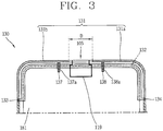
- FIG. 3 is a plan view illustrating an antenna module 130 according to a first embodiment of the present disclosure as a view illustrating the antenna module 130 in FIG. 2A .
- FIGS. 2B through 2D may be substantially analyzed as FIG. 3 though partially different from the mobile terminal illustrated in FIG. 2A , and thus FIG. 3 will be understood and described below as a plan view of FIGS. 2A through 2D .
- the antenna module 130 may include a first conductive member 131 connected to a feeding portion 137 and a grounding portion 138, a second conductive member 132 disposed to be separated from the first conductive member 131, a first connecting member 133 configured to connect the first conductive member 131 to the second conductive member 132 at a position adjacent to the feeding portion 137, and a second connecting member 134 configured to connect the first conductive member 131 to the second conductive member 132 at a position adjacent to the grounding portion 138.
- the feeding portion 137 and grounding portion 138 may be separated from each other by a predetermined distance along the formation direction of the first and the second conductive member 131, 132.
- first conductive member 131 and second conductive member 132 may operate as a radiator of the antenna module 130, and the first conductive member 131 and second conductive member 132 may operate as a radiator of a folded dipole antenna. Furthermore, the first conductive member 131 and second conductive member 132 may be formed with a metal pattern, and may be a microstrip, for an example.
- An input resistance of the folded dipole antenna is larger than that of a half-wave dipole antenna by about four times, and thus the radiation power and radiation resistance thereof increases when compared to those of a typical half-wave dipole antenna. Accordingly, matching to a feeding line having a large characteristic impedance may be facilitated, thereby implementing broadband characteristics.
- first conductive member 131 and second conductive member 132 may be disposed adjacent to the circuit board 181, and at least part of the second conductive member 132 may be disposed to overlap with the circuit board 181.
- a feeding portion As a portion of supplying a current to each member being operated as a radiator, a feeding portion according to an embodiment of the present disclosure may be formed with a combination of a balun, a shifter, a divider, an attenuator, an amplifier, and the like. It will be the same for all feeding portions 137, 237a, 237b which will be described below.
- a feeding method to the conductive member 131, 132 may not be limited in particular.
- the feeding portion 137 to the first conductive member 131 or second conductive member 132 may be electrically connected or the conductive member may be fed in an electro-magnetic feeding method.
- interference may occur between the first conductive member 131, 231 and the second conductive member 132, 232 in a small space, and thus feeding to the conductive member 131, 132, 231, 232 may be preferably provided with direct feeding due to a feeding line.
- the feeding line 137a may include at least one of a feeding plate, a clip for feeding and a feeding line.
- the feeding plate, clip for feeding or feeding line are electrically connected to one another to transfer a current (or voltage) fed through the feeding device to conductive members for transmitting and receiving wireless signals.
- feeding line may include a microstrip printed on a substrate.
- the first conductive member 131 may be divided into a first portion 131a and a second portion 131b, and the first portion 131a and second portion 131b are separated from each other by a predetermined distance (D) to form a slit 105, and the slit 105 is formed between the feeding portion 137 and the grounding portion 138.
- D predetermined distance
- the slit 105 is formed on the first conductive member 131, and it is to shorten the length of the first conductive member 131, thereby more easily implementing a frequency having a high frequency band.
- the slit 105 is sufficiently spaced apart not to cause electrical coupling between the first portion 131a and the second portion 131b. If electrical coupling occurs between the first portion 131a and second portion 131b, it may be difficult to implement a resonant frequency with a low or high frequency band, and thus the first portion 131a and second portion 131b should be spaced apart to the extent that coupling does not occur.
- FIG. 2A relates to a first embodiment of the present disclosure in which the first conductive member 131 forms a lateral appearance of the terminal body, and the second conductive member 132 is formed on the rear case 102.
- the first conductive member 131 may form part or all of a lateral appearance of the terminal body, and maintain the integrity of an appearance design when all of a lateral surface of the terminal body is formed.
- the first and the second connecting member 133, 134 is connected to the first and the second conductive member 131, 132 such that the antenna module 130 is electrically isolated from the remaining portion 102b (refer to FIG. 2B ) excluding the first conductive member 131.
- FIG. 2B illustrates a case where the first conductive member 131 forms part of a lateral appearance of the terminal body, and is separated from the remaining portion 102b by an insulating material 102a, wherein it is grounded to the circuit board 181 at one position of the remaining portion 102b.
- the remaining portion 102b may be a metal deco.
- the remaining portion 102b may form the rear case 102 along with the first conductive member 131 or second conductive member 132.
- the remaining portion 102b may be connected to the first conductive member 131 (second conductive member 132 when the first conductive member 131 is formed on the rear case 102 and the second conductive member 132 forms a lateral appearance of the terminal body) to form a lateral appearance of the terminal body.
- the remaining portion 102b may be formed in a loop shape connected to the first conductive member 131, and formed as the rear case 102 formed into an integral body by insert molding. It is similar to the other embodiments if it is not limited in particular.
- FIG. 2C relates to a first embodiment of the present disclosure, and illustrates a case where the formation positions of the first conductive member 131 and second conductive member 132 are changed with each other, contrary to the case of FIGS. 2A and 2B , and they are the same as in the case of FIGS. 2A and 2B excluding that the positions of the first conductive member 131 and second conductive member 132 are changed.
- the first conductive member 131 and second conductive member 132 may be formed anywhere on a lateral appearance of the terminal body or within the terminal body, and it is sufficient when the slit 105 is formed on either one of the first conductive member 131 and second conductive member 132, and spaced apart by a predetermined distance.
- FIG. 2D relates to a first embodiment of the present disclosure, and illustrates that the second conductive member 132, third connecting member 135 and sub-arm 136 are formed on the rear cover 103.
- the first conductive member 131 forms part or all of a lateral appearance of the terminal body
- the second conductive member 132 is mounted on an inner side of the rear cover 103.
- the sub-arm 136 performs a branch function for parasitic resonance.
- first conductive member 131 and second conductive member 132 may form part or all of a lateral appearance of the mobile terminal, and the first conductive member 131 or second conductive member 132, the third connecting member 135 and sub-arm 136 may be formed on the rear cover 103 or formed on the rear case 102.
- first conductive member 131 or second conductive member 132 may be formed on an inner surface or outer surface of the rear case 102, and may not be necessarily formed on the outermost even when forming a lateral surface of the terminal body.
- the first conductive member 131 may be formed on a lateral surface of the terminal body, but an injection-molded article may be formed on a lateral surface of the outermost, and the first conductive member 131 may be formed within the injection mold.
- first conductive member 131 and second conductive member 132 are spaced apart by a predetermined distance, and may not necessarily form an external appearance of the terminal body.
- the feeding portion 137 may feed the first conductive member 131 to form an antenna loop having various lengths. Due to such a configuration, it may be possible to implement a frequency having a low and a high frequency band.
- FIGS. 2A through 2D are only one example, and thus may be redundantly applied a different embodiment if it is not limited in particular. It is similar to a second embodiment.
- the first conductive member 231 in the second embodiment may form part of all of an lateral appearance of the terminal body, and the second conductive member 232 may be disposed within the terminal body.
- the circuit board 181 may be a flexible circuit board, and the board may be a dielectric substrate or semiconductor substrate, and the ground may be formed on either one surface of the substrate, and any one layer may be the ground when the substrate is a multi-layer substrate. Furthermore, the first and the second conductive member 131, 132 according to an embodiment of the present disclosure is cut along the circuit board 181 to correspond to the structure of the terminal body.
- FIG. 4 is a resonant path of a resonant frequency in a first embodiment of the present disclosure
- FIG. 4A illustrates a first resonant path (L11) capable of implementing a first resonant frequency (F11), wherein the first resonant path (L11) is formed by a current flowing through the first conductive member 131, second conductive member 132, first connecting member 133 and second connecting member 134.
- the first portion 131a and second portion 131b are formed to be spaced apart, and thus the resonant path may include a path connected to the feeding portion 137 and grounding portion 138. It is the same on all resonant paths in a first embodiment described below.
- a position 1318 at which the first connecting member 133 is connected to the first conductive member 131 varies between a portion 1315 connected to the feeding portion 137 and an end of the first conductive member 131 on the first conductive member 131.
- a position at which the first connecting member 133 is connected to the second conductive member 132 may not be limited in particular, but may be preferably connected to the nearest portion 1323 to the first conductive member 131. It is because the first connecting member 133 may be a screw, a C-clip, a pogo pin, an EMI sheet, or the like as will be described later.
- the first conductive member 131 may be connected to the second conductive member 132 by a conductive pattern, and in this case, the first connecting member 133 may not be formed at a recent contact point between the first conductive member 131 and second conductive member 132.
- FIGS. 2A through 2D illustrate a case where the third connecting member 135 is a conductive pattern.
- a position at which the second connecting member 134 is connected to the first conductive member 131 varies between a portion 1316 connected to the grounding portion 138 through a grounding line 138a on the first conductive member 131 and an end of the first conductive member 131.
- the frequency band may vary by varying the formation positions of the first connecting member 133 and second connecting member 134.
- the first connecting member 133 may be formed at an end of the first conductive member 131 and/or second conductive member 132, and formed at any one position of the middle portion thereof.
- a first through a fourth parasitic arm 1313, 1314, 1321, 1322 may be formed. In this manner, the first connecting member 133 and second connecting member 134 may be minutely moved to tune the frequency.
- the efficiency and impedance characteristics of frequency band may be determined by the first through the fourth parasitic arm 1313, 1314, 1321, 1322.
- the first through the fourth parasitic arm 1313, 1314, 1321, 1322 denote a portion passing through the first and the second connecting member 133, 134.
- FIG. 4B illustrates a second resonant path (L12) capable of implementing a second resonant frequency (F12), wherein the second resonant frequency (F12) is higher than the first resonant frequency (F11).
- the second resonant frequency (F12) is formed along the first conductive member 131, second conductive member 132, first connecting member 133 and third connecting member 135.
- the third connecting member 135 is formed to implement the second resonant path (L12).
- one end portion thereof may be connected to the first conductive member 131, and the other end portion thereof may further include the third connecting member 135 connected to the second conductive member 132.
- a position 1317 at which the third connecting member 135 is connected to the first conductive member 131 varies between a portion 1316 connected to the grounding portion 138 through a grounding line 138a and a portion 1319 connected to the second connecting member 134 on the first conductive member 131
- a position 1325 at which the third connecting member 135 is connected to the second conductive member 132 varies between a portion 1323 connected to the first connecting member 133 and a portion 1324 connected to the second connecting member 134 on the second conductive member 132.
- a resonant length thereof may be changed to change the resonant frequency.
- a slight change in position may be allowed to obtain a required resonant frequency.
- the second resonant path (L12) is formed with a path flowing between the feeding portion 137 and the grounding portion 138 due to the effect of the slit 105 formed on the first conductive member 131, similarly to the first resonant path (L11).
- the antenna module 130 is a type of folded dipole antenna, and thus the first conductive member 131 and second conductive member 132 may be formed with a predetermined length to resonate at a first and a second frequency, an antenna length of the resonance may be formed to have a length of about ⁇ /2 corresponding to a first and a second frequency. However, as will be described later, it has a length of about ⁇ /4 when operated as a monopole antenna.
- the first frequency is a low frequency
- the second frequency is a high frequency which is higher than the first frequency
- the first frequency may be a frequency band of about 700 through subject 1200 MHz which is a low frequency band
- the second frequency may be a frequency band of about 1710 through subject 27000 MHz which is a high frequency band.
- it may be also divided into a low frequency band of about 700 through 1000 MHz, a mid frequency band of 1700 through 2200 MHz, and a high frequency band of 2200 through 2700 MHz.
- a current fed to the first conductive member 131 is transferred to the second conductive member 132 through the first connecting member 133.
- a current transferred to the second conductive member 132 flows to the first conductive member 131 again through the second connecting member 1340, and then enters the ground of the circuit board 181 through the grounding portion 138.
- the antenna module 130 When the antenna module 130 is seen from a different point of view based on the flow of such a current, it may be simplified to a current flowing to the first conductive member 131 and second conductive member 132 in the same direction.
- the antenna module 130 of the present disclosure may function as a folded dipole antenna having a shape in which a folded portion is added to a half-wave dipole antenna, and the first conductive member 131 and second conductive member 132 may be electrically symmetrical. It is similar to a second embodiment which will be described later.
- a third resonant path may be formed on the first conductive member 131, but formed as a path for connecting the feeding portion 137 to the grounding portion 138 in the vicinity of the slit 105 of the first conductive member 131.
- the slit 105 may be formed on the first conductive member 131, and as illustrated in FIG. 4D , a fourth resonant path (L14) may be formed by a feeding line 137a connecting the feeding portion 137 to the first conductive member 131 and a path formed with an open end 1311 of the second portion 131b forming the slit 105 to implement a fourth resonant frequency (F14).
- L14 fourth resonant path
- a fifth resonant frequency may be implemented by a grounding line 138a connecting the grounding portion 138 to the first conductive member 131 and an open end 1312 of the first portion 131a forming the slit 105.
- the grounding line 138a may include at least one of a grounding plate, a clip for grounding and a grounding line as an electrical path connecting the grounding portion 138 and the first conductive member 131. It is the same for all grounding portions in the first and the second embodiment of the present disclosure.
- the sub-arm 136 may be formed on the first conductive member 131 to implement a higher resonant frequency.
- one end portion may be connected to the first conductive member 131, and the other end portion may include an open sub-arm 136.
- the formation position 1320 of one end portion of the sub-arm 136 is formed between a portion 1316 connected to the grounding portion 138 through the grounding line 138a and a portion 1317 connected to the third connecting member 135 on the first conductive member 131.
- a sixth resonant path (L16) formed from the grounding line 138a to an open end of the sub-arm 136 passing through the first conductive member 131 may be formed to implement a sixth resonant frequency (F16).
- one end portion of the sub-arm 127' may be ground-connected to the circuit board 181, and the other end portion thereof may be open. It will be described later.
- the slit 105 may be formed on the first conductive member 131 to facilitate the implementation of a high frequency band as well as a low frequency band.
- one end portion of the sub-arm 136 may not be necessarily limited to this.
- one end portion of the sub-arm 136 may vary between a portion 1317 connected to the third connecting member 135 and a portion 1319 connected to the second conductive member 132 on the first conductive member 131.
- a resonant path may be changed to change the resonant frequency.
- the fourth through the sixth resonant frequency (F14, F15, F16) is operated as a monopole antenna an end of which is open, and the antenna length may have a length of about ⁇ /4 corresponding to a resonant frequency.
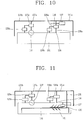
- FIG. 10 is a conceptual view illustrating part of an antenna module 130 according to a first embodiment of the present disclosure, and will be described below with reference to FIG. 10 .
- a first matching module 125a for impedance matching is disposed on the feeding line 137a connected to the feeding portion 137 to feed the first conductive member 131, and a first variable switch 125b for controlling a current flowing through the first portion 131a is connected to the first matching module 125a.
- the first variable switch 125b may be connected to the first matching module 125a in series or in parallel.
- a second matching module 126a for impedance matching is disposed on the grounding line 138a connected to the grounding portion 138 to ground the first conductive member 131, and a second variable switch 126b for controlling a current flowing through the first portion 131a is connected to the second matching module 126a in series or in parallel.
- a third variable switch 136 for controlling a current flowing through the sub-arm 136 may be formed on the sub-arm 136.
- variable switch may be formed on the third connecting member 135.
- a desired resonant frequency may be implemented by changing the formation position of the third connecting member 135, and there is a case where the variable switch may not be formed.
- the foregoing first matching module 125a and second matching module 126a may be formed with a combination of an inductor and a capacitor, and implemented with series or shunt elements.
- a reactance value which is an imaginary part of impedance may be changed.
- an inductor increases the reactance and a capacitor decreases the reactance, and thus the impedance at a specific frequency band may be changed.
- a resistance value which is a real part of impedance may be changed.
- the inductor increases the resistance value and the capacitor decreases the resistance value to change the impedance at a specific frequency band.
- FIG. 6 is a conceptual view illustrating a modified example of an antenna module 130 according to a first embodiment of the present disclosure, and illustrates a case where the positions of the first conductive member 131 and second conductive member 132 are changed with each other, contrary to the foregoing case.
- the lateral surface of the mobile terminal may be streamlined for a sleek look to provide an elegant appearance.
- An exploded perspective view of a mobile terminal associated therewith is illustrated in FIG. 2C .
- the slit 105 should be spaced apart to the extent that coupling does not occur.
- a portion formed with the slit 105 may be a problem, but an interface unit 119 such as a USB port may be formed at the portion formed with the slit 105, and thus the appearance is not greatly affected.
- an adjoining portion of the interface unit 119 is separated from the first portion 131a and second portion 131b, and thus a current does not flow.
- the slit is formed within the mobile terminal 100 and thus not exposed to the outside.
- FIG. 6 illustrates only a portion shown in FIG. 4A to be easily compared with FIG. 4A , and the matching modules 125a, 126a and variable switches 125b, 126b, 27) are not shown as illustrated in FIGS. 10 and 11 , but the addition of those configurations may not be limited in particular.
- the modified example illustrated in FIG. 6 is not shown in detail, the items illustrated in FIGS. 10 and 11 may be applicable as it is.
- a first matching module may be disposed at a portion connected to the feeding portion 137 and second portion 131b in FIG. 6
- a second matching module may be disposed at a portion connected to the grounding portion 138 and first portion 131a in FIG. 6
- a first and a second variable switch may be provided in the first and the second matching module, respectively.
- a third variable switch may be also provided in the sub-arm 136 illustrated in FIG. 6 .
- FIG. 11 is a conceptual view illustrating another modified example of an antenna module 130 according to a first embodiment of the present disclosure, and illustrates that the sub-arm 136' is ground-connected to the circuit board 181 which is the ground, and the variable switch 127' is formed on the sub-arm 136'.
- the sub-arm 136' and second conductive member 132 are formed to be separated from each other to generate electromagnetic coupling, thereby adding a resonant frequency band.
- at least part of the sub-arm 136' may be formed in parallel to the second conductive member 132 to further generate electromagnetic coupling.
- FIG. 12 is a view illustrating the type of variable switches according to an embodiment of the present disclosure, in which they are formed with various combinations of a capacitor and an inductor.
- the variable switch may have inductors with different sizes as illustrated in FIG. 12A , or have an inductor and a capacitor as illustrated in FIG. 12B , or have only one inductor as illustrated in FIG. 12C .
- an inductor and a variable capacitor are connected in series as illustrated in FIG. 12D , and have a variable capacitor as illustrated in FIG. 12E , and an inductor and a variable capacitor are connected in parallel as illustrated in FIG. 12F .
- variable inductor may be used, and a single pole double throw (SPDT) switch and a single pole triple throw (SP3T) switch may be also used.
- SPDT single pole double throw
- SP3T single pole triple throw
- FIG. 5 is a conceptual view and a partially enlarged view illustrating an antenna module 130 according to a first embodiment of the present invention, in which the first conductive member 131 in a first embodiment of the present disclosure may form a lateral appearance of the mobile terminal, and the second conductive member 132 may be disposed within the terminal body.
- FIG. 7 is a graph illustrating a reflection coefficient according to a frequency of an antenna module 130 according to a first embodiment of the present disclosure, and it is seen that the antenna module resonates at a first through a third resonant frequency (F11, F12, F13) in the vicinity of 700 MHz, 800 MHz and 1200 MHz, and resonates at a fourth through a sixth resonant frequency (F14, F15, F16) in the vicinity of 1900 MHz, 2200 MHz and 2700 MHz.
- F11, F12, F13 a third resonant frequency
- F14, F15, F16 sixth resonant frequency
- FIG. 8 is an enlarged view illustrating portion "A" shown in FIG. 1C
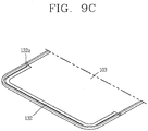
- FIG. 9A is a conceptual view illustrating in which only a first conductive member 131 is separated from FIG. 8
- FIGS. 9B and 9C are conceptual views in which only a rear cover 103 is separated from FIG. 8 .
- the first conductive member 131 is electrically connected to the second conductive member 132 through the first connecting member 133.
- a structure which will be described below may be similarly applicable to an electrical connecting structure between the first conductive member 131 and the second conductive member 132 through the second connecting member 134.
- the first connecting member 133 is mounted either one of the rear cover 103 and first conductive member 131, and allowed to electrically connect the first conductive member 131 to the second conductive member 132 through a contact with the other one.
- the second conductive member 132 and the first conductive member 131 may be electrically connected to each other due to the contact, and the contact may be securely maintained due to elastic deformation.
- a C-clip, a pogo pin or EMI sheet may be used for the first and the second connecting member 131, 132.
- the first connecting member 133 may be mounted at an inner side of the rear cover 103 or mounted on the rear case 102 as illustrated in FIG. 2D .
- FIGS. 8 , 9A through 9C illustrate that the second conductive member 132 is provided in the rear cover 103, and it may be configured such that the first connecting member 133 is mounted on the first conductive member 131 to be protruded from the first conductive member 131.
- the first connecting member 133 may be accommodated into the first conductive member 131 in such a manner that at least part 133a thereof is disposed to be protruded from the first conductive member 131.
- the first connecting member 133 may be coupled to an inner surface of the first conductive member 131 in such a manner that at least part thereof is disposed to be protruded from the first conductive member 131 or to cover an upper surface of the first conductive member 131.
- FIG. 9B it may be configured such that the first connecting member 133 protruded from either one of the rear cover 103 and first conductive member 131 to be inserted into the groove 103a formed on the other one.
- FIG. 9B is a perspective view in which an inner portion of the rear cover 103 is seen, and as illustrated in FIG. 9B , a groove 103a corresponding to the first connecting member 133 may be formed on the rear cover 103.
- the groove 103a is configured to accommodate the first connecting member 133.
- Part of the second conductive member 132 may be exposed to the outside through the groove 103a.
- the second conductive member 132 forms a bottom portion of the groove 103a.
- the second conductive member 132 may be formed to traverse the rear cover 103.
- the first connecting member 133 may be electrically connected to the second conductive member 132 even when the first connecting member 133 formed on the rear case 102 is slightly exposed to the outside.
- a method of connecting the first and the second conductive member131, 132 may not be limited.
- the extension portion 132a is formed as described above for more efficient contact.
- the first connecting member 133 may not only electrically connect the first conductive member 131 to the second conductive member 132 but also be inserted into the groove 103a such that that rear cover 103 is securely fixed to the rear case 102.
- the first conductive member 131 may be coupled to the second conductive member 132 using a screw (not shown) to further secure the first conductive member 131 and second conductive member 132.
- FIG. 13 is a conceptual view illustrating an antenna module 230 according to a second embodiment of the present disclosure, and will be described below with reference to FIG. 13 .
- the first conductive member 231 may form a lateral appearance of the terminal body, and the second conductive member 232 may be formed within the terminal body. It is similar to the drawings of FIGS. 2A through 2D , and thus the description thereof will be substituted by the earlier description of FIGS. 2A through 2D .
- block members 211, 212 are added to independently implement a high and a low band resonant frequency by two feeding portions 237a, 237b.
- two feeding portions 237a, 237b it will be described in more detail.
- An antenna module 230 may include a first conductive member 231 fed by a first feeding portion 237a, a second conductive member 232 disposed to be separated from the first conductive member 231, and fed by a second feeding portion 237b, a first connecting member 233 connected to one side of the first conductive member 231 and second conductive member 232, and a second connecting member 234 connected to one middle position between the first conductive member 231 and second conductive member 232.
- the first connecting member 233 is formed at a position adjacent to the first feeding portion 237a, and one end portion thereof is connected to the first conductive member 231, and the other end portion thereof is connected to the second conductive member 232, and a position of the one end portion varies between a portion 2312 connected to the first feeding portion 237a and an end of the first conductive member 231 on the first conductive member 231, and a position of the other end portion varies between a portion 2323 connected to the second feeding portion 237b and an end of the second conductive member 232 on the second conductive member 232.
- the second connecting member 234 varies between a position at which the second connecting member 234 is connected to the second conductive member 232 and an end of the second conductive member 232.
- the first and the second connecting member 233, 234 may vary a resonant frequency band according to the variation of the position, and though reference numerals are not designated herein, a parasitic arm may be formed at a portion in which the first connecting member 233 is connected to the first and the second conductive member 231, 232.
- the first connecting member 233 may be connected to an end of the first and the second conductive member 231, 232, and may be connected to one middle position thereof, and a parasitic arm may be formed when the first connecting member 233 is connected to a middle position between the first and the second conductive member 231, 232.
- the resonant frequency may be minutely tuned by the parasitic arm as in the first embodiment.
- one end portion thereof is connected to the first conductive member 231, and the other end portion thereof is connected to the second conductive member 232.
- the one end portion thereof varies between a portion 2312 connected to the first feeding portion 237a through a first feeding line 2371 and a portion 2311 connected to the first connecting member 233 through the first conductive member 231 on the first conductive member 231, and the other portion thereof varies between a portion 2323 at which the second feeding portion 237b is connected to the second conductive member 232 through a second feeding line 2372 and a portion 2321 at which the first connecting member 233 is connected to the second conductive member 232 on the second conductive member 232.
- first conductive member 231 and second conductive member 232 are open at a position adjacent to the 237b.
- the first feeding portion 237a and second feeding portion 237b may implement resonant frequencies at different band frequencies without interfering with each other.
- the first feeding portion 237a may feed the first conductive member 231 to implement a resonant frequency at a lower frequency band
- the second feeding portion 237b may feed the second conductive member 232 to implement a resonant frequency at a higher frequency band.
- an end portion of the first conductive member 231 and second conductive member 232 is open.
- an open end of the first conductive member 231 may form a lateral appearance of the terminal body.
- an open end of the first conductive member 231 may be formed into an integral body with a lateral surface of the terminal body.
- FIG. 14 illustrates a resonant path according to a second embodiment of the present disclosure, in which a first resonant path (L21) is formed by the first conductive member 231 to implement a first resonant frequency (F21).
- the first conductive member 231 and second conductive member 232 form a folded dipole antenna, and thus an input resistance of the folded dipole antenna is larger than that of a half-wave dipole antenna by about four times, and thus the radiation power and radiation resistance thereof increase four times compared to those of a half-wave dipole antenna. Accordingly, matching to a feeding line having a large characteristic impedance may be facilitated, thereby implementing broadband characteristics.
- first conductive member 231, second conductive member 232 and second connecting member 234 may implement a second resonant path (L22) to implement a second resonant frequency (F22).
- the first conductive member 231 is earthed to the ground through a grounding line 2381, and a second variable switch 226 is formed on the grounding line 2381, thereby forming a third resonant path (L23).
- a third resonant frequency (F23) may be implemented by the third resonant path (L23) that is formed as an open end of the first conductive member 231 starting from the grounding line 2381 and then passing through a portion 2314 at which the grounding line 2381 is connected to the first conductive member 231.
- a second embodiment of the present disclosure it is allowed to resonate even at a frequency band other than the first through the third resonant frequency (F21, F22, F23), and a configuration in which a resonant frequency implemented by the first feeding portion 237a and a resonant frequency implemented by the second feeding portion 237b do not electromagnetically affect each other is added.
- the conductive members 231, 232 are formed within a smaller space, the frequency band can be extended using interference between the conductive members 231, 232.
- a first block member 211 formed between a portion 2322 connected to the second connecting member 234 and a portion 2323 connected to the second feeding portion 237b through the second feeding line 2372 on the second conductive member 232 to block a current generated from the second feeding portion 237b from flowing to the first feeding portion 237a is added, and a second block member 212 formed on the second feeding line 237b connected to the second feeding portion 237b to feed the second conductive member 232 to block a current generated from the first feeding portion 237a from flowing to the second feeding portion 237b is further added.
- the frequency band can be independently implemented by the first block member 211 and second block member 212.
- a current may be blocked by the first block member 211 and second block member 212, thereby allowing a current due to the second feeding portion 237b to implement a fifth resonant frequency (F24) by a fourth resonant path (L24) formed up to an end of the first block member 211 and second conductive member 232.
- the second embodiment of the present disclosure forms the sub-arm 236, in which the sub-arm 236 is formed on the second conductive member 232, and one end portion thereof is formed between a portion 2323 connected to the second feeding portion 237b and an open end adjacent to the second feeding portion 237b among the open ends of the second conductive member 232, and the other end portion thereof is open.
- a fifth resonant frequency (L25) is formed due to the sub-arm 236 fed by the second feeding portion 237b.
- the fifth resonant frequency (L25) is formed on the second feeding line 2372 connected to the second conductive member 232 from the second feeding portion 237b, the second conductive member 232, and the sub-arm 236, thereby implementing a fifth resonant frequency (L25).
- the position of the sub-arm 236 may not be necessarily limited to the position.
- one end portion of the sub-arm 236 may vary between a portion 2323 connected to the second feeding portion 237b and the first block member 211 on the second conductive member 232.
- a resonant path may be changed to change the resonant frequency.
- a sixth resonant path may be formed by the first connecting member 233, second connecting member 234, first conductive member 231 and second conductive member 232, thereby implementing a sixth resonant frequency.
- FIG. 15 is a graph illustrating a reflection coefficient according to a frequency associated with a second embodiment of the present disclosure, and it is seen that the antenna module resonates at 700 MHz, 800 MHz, 1600 MHz, 1900 MHz, 2300 MHz and 2450 MHz.
- the result illustrates only one embodiment, and the present disclosure may not be necessarily limited to those resonant frequencies in interpreting the right scope of the present disclosure.
- matching modules may be disposed to tune each resonant frequency.
- a first matching module 225a may be formed on the first feeding line 2371 for feeding the first conductive member 231, and for the first matching module 225a, a first variable switch 225b for controlling a current flowing through the first conductive member 231 may be connected to the first matching module 225a in series or in parallel.
- the first variable switch 225b and second variable switch 226 may be formed with a combination of an inductor and a capacitor as illustrated in the foregoing drawing of FIG. 12 .
- a block member for blocking the flow of a current may include one or more lumped element.
- an inductor or capacitor may be used, and a conductive pattern may be formed on a substrate to operate as a capacitor and an inductor, respectively.
- the block member may block an antenna module from resonating at a specific frequency band. Furthermore, even when the antenna module resonates in actuality, the block member may block a signal due to resonance from being introduced to and radiated from the mobile terminal. For example, when the block frequency band of the block member is F1 or F2, the antenna module may be formed to block signals within F1 or F2 band.
- the block member 211, 212 is basically seen as a type of filter to block frequencies in a specific band, and the block member 211, 212 may be formed with a combination of an inductor and a capacitor in series or in parallel.
- the block member When the block member includes one or more inductors, it may block signals corresponding to frequencies higher than F1 in the block frequency band (F1 or F2), and when the block member includes one or more capacitors, it may block signals corresponding to frequencies lower than F1 in the block frequency band (F1 or F2). Furthermore, when the block member is combined with an inductor and a capacitor, it may block the antenna module 230 from resonating at a specific frequency band.
- the block member may include a capacitor, an inductor and a switching element, wherein the switching element may selectively switches the capacitor and inductor or connect the capacitor and inductor at the same time. Moreover, specific frequencies may be blocked with a combination including the inductor and/or capacitor, wherein the capacitor is a variable capacitor.
- the first block member 211 may be a type of low pass filter formed to include an inductor that passes only resonant frequencies lower than a specific frequency without passing resonant frequencies higher than the specific frequency
- the second block member 212 may be a type of high pass filter formed to include a capacitor that passes only resonant frequencies higher than a specific frequency without passing resonant frequencies lower than the specific frequency.
- first and the second block member 211, 212 are only required to block resonant frequencies at a specific frequency band, respectively, and may be a band pass filter for passing resonant frequencies having a predetermined bandwidth or a notch filter for blocking resonant frequencies at a specific band.
- the second block member 232 including a capacitor is formed on the second feeding line 2372, and the second block member 231 including an inductor is formed on the second conductive member 232, but it is disposed in a such a manner that resonant frequencies in a high frequency band are mainly implemented by the second feeding portion 237b and resonant frequencies in a low frequency band are mainly implemented by the first feeding portion 237a. Accordingly, when the first feeding portion 237a implements resonant frequencies in a high frequency band, the first block member 211 may include a capacitor to block frequencies in a low frequency band, and the second block member 212 may include an inductor to block frequencies in a high frequency band.
- the sub-arm 236 may be formed adjacent to the first conductive member 231 to be separated therefrom so as to generate electric coupling with the first conductive member 231.
- the first conductive member 231 and sub-arm 236 may be formed adjacent to each other in parallel.
- electrical coupling is generated between a current formed at an open end of the first conductive member 231 adjacent to the second feeding portion 237b to extend the frequency band and a current formed on the sub-arm 236 to form a third resonant path (L23).
- the flows of each current implementing a high frequency band and a low frequency band, respectively exert an effect on each other to form an additional resonant path (L23), thereby having an advantage in the aspect of space use.
- a high frequency band can be optimally designed.
- a mobile terminal having an antenna module 130, 230 in the foregoing first embodiment and second embodiment.
- a mobile terminal having the antenna module 130 according to the first embodiment is referred to as a third embodiment
- a mobile terminal having the antenna module 230 according to the second embodiment is referred to as a fourth embodiment.
- the antenna module 130 is formed on a body of the mobile terminal, and formed to operate at a first frequency and a second frequency.
- the first frequency may be frequencies in a low frequency band and the second frequency be frequencies in a high frequency band.
- the antenna module 130 may include the first and the second connecting member 133,134 connecting both ends of the first conductive member 131 and second conductive member 132 and the first conductive member 131 and second conductive member 132, respectively, and the first conductive member 231 is connected to the feeding portion 137 and grounding portion 138, and the slit 105 is formed on the first conductive member 131, wherein the slit 105 is formed between the feeding portion 137 and grounding portion 138.
- first conductive member 131 and second conductive member second conductive member 132 form a lateral appearance of the terminal body or is formed within the terminal body.
- the second conductive member 132 is disposed within the terminal body, and when the second conductive member 132 is disposed within the terminal body, the second conductive member 132 may form a lateral appearance of the terminal body.
- the first conductive member 131 or second conductive member 132 may form part or all of a lateral surface of the terminal body. If the first conductive member 131 or second conductive member 132 forms part of a lateral surface of the terminal body, an insulating material 102a may be formed to be separated from the remaining portion 102b of the lateral surface of the terminal body by a predetermined distance. Furthermore, when the remaining portion 102b of the lateral surface of the terminal body is made of a metal, the remaining portion 102b may be preferably earthed to the ground not to affect on the antenna module 130.
- first conductive member 131 or second conductive member 132 forms the entire lateral appearance of the terminal body
- first conductive member 131 and the remaining portion 102b may be separated by the first connecting member 133 and second connecting member 134, and thus an additional grounding line may not be required, and they seem to be formed into an integral body when seen from the outside. Accordingly, an end portion of the first conductive member 131 is shown as a dotted line in FIGS. 2A , 2C and 2D .
- the first conductive member 131, 231 or second conductive member 132, 232 may form a lateral appearance of the terminal body, and when forming a lateral appearance of the terminal body, an additional slit is not required if the material of the remaining portion 102b is a material different from the first conductive member 131, 231 and second conductive member 132,232, in particular, a polycarbonate material.
- a slit may be formed between the first or the second conductive member 131, 132, 231, 232 and the remaining portion 102b or should be grounded at one side of the first or the second conductive member 131, 132, 231, 232 as in the foregoing first embodiment and second embodiment.
- the first conductive member 131 and second conductive member 132 may be made on planes, and the planes, respectively, may be formed to be perpendicular to each other. In other words, as illustrated in FIGS. 2A through 2D , the first conductive member 131 and second conductive member 132 may be formed on planes, and made perpendicular to each other.
- the present disclosure may not be necessarily limited to this.
- the first conductive member 131 and second conductive member 132 may be disposed within the terminal body without forming a lateral appearance of the terminal body, and they may not be formed to be perpendicular to each other on at least part thereof.
- two planes of the first and the second conductive member 131, 132, 231, 232 may be formed in parallel to each other.
- the first conductive member 131 forms a lateral appearance of the terminal, it is formed along the shape of the mobile terminal, and thus at least part of the edge portion thereof may be formed with a curved surface.
- the second conductive member 132 may be formed in a non-uniform pattern, and it is to efficiently carry out impedance matching.
- the second conductive member 132 may include a step shape, thereby forming an area thereof to be different along the formation path of the second conductive member 132.
- the antenna module may further include the third connecting member 135 one end portion of which is connected to the second conductive member 132 and the other portion of which is connected to the first conductive member 131.
- a position 1317 at which the third connecting member 135 is connected to the first conductive member 131 varies a portion 1316 connected to the grounding portion 138 and a portion 1319 connected to the second connecting member 234 on the first conductive member 131, and a position at which the first connecting member 133 is connected to the second conductive member 132 varies between a portion 1323 connected to the first connecting member 133 and a portion 1324 connected to the second connecting member 134 on the second conductive member 132.
- a position 1325 at which the first connecting member 133 is connected to the first connecting member 133 may be preferably formed adjacent to the portion 1324 connected to the second connecting member 134 or the grounding portion 138.
- the antenna module may further include the sub-arm 236 one end portion of which is connected to the first conductive member 231, and the other end portion of which is open, wherein one end portion of the sub-arm 136 is formed between a portion 1316 connected to the grounding portion 138 through the grounding line 138a and a portion 1317 connected to the third connecting member 135 on the first conductive member 131.
- a mobile terminal according to a fourth embodiment may include a terminal body and an antenna module 230 formed to operate in a first frequency band and in a second frequency band different from the first frequency band.
- the antenna module 230 may include the first and the second conductive member 231, 232 fed by the first and the second feeding portion 237a, 237b, respectively, the first connecting member 233 connecting the first conductive member 231 to the second conductive member 232 at a position adjacent to the first feeding portion 237a, and the second connecting member 234 one end portion of which is connected to the first conductive member 231 and the other portion of which is connected to the second conductive member 232.
- the position of the one end portion of the second connecting member 234 varies between a portion 2313 connected to the first feeding portion 237a and a portion 2311 at which the first connecting member 233 is connected to the first conductive member 231, and the position of the other end portion varies between a portion 2323 at which the second feeding portion 237b is connected to the second conductive member 232 and a portion 2321 at which the first connecting member 233 is connected to the second conductive member 232.
- the antenna module may further include the first block member 211 formed between a portion 2322 connected to the second connecting member 234 and a portion 2323 connected to the 237b on the second conductive member 232 to block a current generated from the second feeding portion 237b from flowing to the first feeding portion 237a, and the second block member 212 formed on the second feeding line 2372 connected to the first feeding portion 237a to feed the second conductive member 232 so as to block a current generated from the first feeding portion 237a from flowing to the second feeding portion 237b.
- the first conductive member 231 in the fourth embodiment may form a lateral appearance of the terminal body, and the second conductive member 232 may be disposed within the terminal body.
- the first conductive member 231 may be formed within the terminal, and the second conductive member 232 may form a lateral appearance of a lateral surface of the terminal body.
- first conductive member 231 or second conductive member 232 forms a lateral appearance of the terminal body
- part or all of the lateral appearance of the terminal body may be formed, and separated from the remaining portion 102b (refer to FIG. 2 ) of the terminal body by a predetermined distance when forming part thereof, and preferably earthed to the ground not to allow the remaining portion 102b to affect on the antenna module 230.
- one side of a lateral surface of the terminal body may be electrically separated from the inside of the terminal body by the first connecting member 233.
- the first connecting member 133 and second connecting member 134 according to the first and the third embodiment of the present disclosure may be a simple fastening means such as a screw, a C-clip, a pogo pin, an EMI sheet or the like, and may not be necessarily limited in particular if it is an electrically connected means. It is similar to a case of the first connecting member 233 according to the second and the fourth embodiment.
- the second connecting member 234 according to the second and the fourth embodiment may be also a simple fastening means such as a screw, a C-clip, a pogo pin, an EMI sheet or the like, but preferably formed with a metal pattern due to the characteristic of connecting the first conductive member 231 to the second conductive member 232.
- the method of connecting the metal pattern to the first conductive member 231 and second conductive member 232 may be carried out using a simple fastening means such as a screw, a C-clip, a pogo pin, an EMI sheet or the like.
- An antenna module 130, 230 according to the first through the fourth embodiment of the present disclosure and a mobile terminal including the same may provide an excellent performance to a narrow bezel, and it is due to an effect of the second conductive member 132, 232.
- antenna efficiency may be enhanced as increasing a distance between a radiator which is the conductive member 131, 132, 231, 232 and a printed circuit board 181, 281 which is the ground. Accordingly, when having a narrow bezel, a distance between the conductive member 131, 132, 231, 232 and the printed circuit board 181, 281 is decreased, thereby reducing antenna efficiency.
- a current intensity that has been weaken by the current (11) flowing through the first conductive member 131 and the current (I3) flowing through the circuit board 181 is reinforced by an overlapping effect of the current (12) flowing through the second conductive member 232 and the current (13) flowing through the circuit board 181, and as a result, even in case of a mobile terminal having a narrow bezel, it may be possible to implement an antenna efficiency similar to that having a wide bezel.
- the foregoing present invention may be implemented as codes readable by a computer on a medium written by the program.
- the computer-readable media may include all kinds of recording devices in which data readable by a computer system is stored. Examples of the computer-readable media may include a hard disk drive (HDD), a solid state disk (SSD), a silicon disk drive (SDD), a ROM, a RAM, a CD-ROM, a magnetic tape, a floppy disk, and an optical data storage device, and the like, and also include a device implemented in the form of a carrier wave (for example, transmission via the Internet).
- the computer may include the controller 180 of the mobile terminal. Accordingly, the detailed description thereof should not be construed as restrictive in all aspects but considered as illustrative. The scope of the invention should be determined by reasonable interpretation of the appended claims.
Landscapes
- Engineering & Computer Science (AREA)
- Computer Networks & Wireless Communication (AREA)
- Telephone Set Structure (AREA)
- Support Of Aerials (AREA)
Applications Claiming Priority (1)
| Application Number | Priority Date | Filing Date | Title |
|---|---|---|---|
| KR1020140173074A KR20160067541A (ko) | 2014-12-04 | 2014-12-04 | 안테나 모듈 및 이를 이용한 이동 단말기 |
Publications (3)
| Publication Number | Publication Date |
|---|---|
| EP3029767A2 EP3029767A2 (en) | 2016-06-08 |
| EP3029767A3 EP3029767A3 (en) | 2016-08-10 |
| EP3029767B1 true EP3029767B1 (en) | 2019-10-16 |
Family
ID=53174758
Family Applications (1)
| Application Number | Title | Priority Date | Filing Date |
|---|---|---|---|
| EP15001330.8A Active EP3029767B1 (en) | 2014-12-04 | 2015-05-05 | Antenna module and mobile terminal using the same |
Country Status (5)
| Country | Link |
|---|---|
| US (1) | US9685694B2 (ko) |
| EP (1) | EP3029767B1 (ko) |
| JP (1) | JP6513478B2 (ko) |
| KR (1) | KR20160067541A (ko) |
| CN (1) | CN106207446A (ko) |
Families Citing this family (38)
| Publication number | Priority date | Publication date | Assignee | Title |
|---|---|---|---|---|
| CN105406196B (zh) * | 2015-10-26 | 2018-04-03 | 瑞声精密制造科技(常州)有限公司 | 天线模组及采用该天线模组的移动终端 |
| US10128574B2 (en) * | 2015-11-24 | 2018-11-13 | Aac Acoustic Technologies (Shenzhen) Co., Ltd | Antenna tuning assembly and mobile communication apparatus using same |
| WO2017090997A1 (ko) | 2015-11-27 | 2017-06-01 | 엘지전자 주식회사 | 이동 단말기 |
| WO2017101068A1 (zh) * | 2015-12-17 | 2017-06-22 | 华为技术有限公司 | 一种移动通讯终端 |
| TWI631768B (zh) * | 2016-06-20 | 2018-08-01 | 川益科技股份有限公司 | 通訊裝置及其天線組件 |
| KR102586130B1 (ko) * | 2016-09-08 | 2023-10-10 | 주식회사 뉴파워 프라즈마 | 복수의 와이어 패턴을 이용한 nfc 안테나 모듈 |
| KR102583716B1 (ko) * | 2016-09-12 | 2023-10-04 | 삼성전자주식회사 | 안테나 장치 및 그것을 포함하는 전자 장치 |
| US10511083B2 (en) | 2016-09-22 | 2019-12-17 | Apple Inc. | Antennas having symmetrical switching architecture |
| WO2018058300A1 (zh) * | 2016-09-27 | 2018-04-05 | 北京小米移动软件有限公司 | 终端壳体及终端 |
| WO2018075578A1 (en) * | 2016-10-21 | 2018-04-26 | Cavendish Kinetics, Inc | Multi-resonant antenna structure |
| US10879588B2 (en) * | 2016-12-27 | 2020-12-29 | Htc Corporation | Mobile device and manufacturing method thereof |
| DE102017131182A1 (de) | 2016-12-27 | 2018-06-28 | Htc Corporation | Mobile Vorrichtung und Herstellungsverfahren für diese |
| CN107069212B (zh) * | 2017-01-23 | 2021-02-23 | 瑞声科技(南京)有限公司 | 天线装置及应用该天线装置的移动终端 |
| CN110249482B (zh) * | 2017-01-26 | 2021-04-23 | Lg电子株式会社 | 移动终端 |
| WO2018139691A1 (ko) * | 2017-01-26 | 2018-08-02 | 엘지전자 주식회사 | 이동 단말기 |
| CN106848594B (zh) * | 2017-03-06 | 2019-10-11 | 北京小米移动软件有限公司 | 天线模块及电子设备 |
| KR102307730B1 (ko) * | 2017-04-10 | 2021-10-05 | 삼성전자주식회사 | 전자 장치의 하우징에 포함된 도전성 물질을 이용하는 안테나를 포함하는 전자 장치 |
| KR102393808B1 (ko) * | 2017-06-20 | 2022-05-04 | 삼성전자주식회사 | 안테나를 포함하는 전자 장치 |
| CN107317113A (zh) | 2017-06-27 | 2017-11-03 | 北京小米移动软件有限公司 | 天线模块及电子设备 |
| JP6925934B2 (ja) * | 2017-10-26 | 2021-08-25 | 京セラ株式会社 | 通信ユニット |
| EP3726818A4 (en) * | 2017-12-12 | 2021-07-28 | LG Electronics Inc. | ANTENNA DEVICE AND MOBILE TERMINAL WITH IT |
| JP7124097B2 (ja) * | 2018-03-20 | 2022-08-23 | ホアウェイ・テクノロジーズ・カンパニー・リミテッド | アンテナエクステンダ及びアンテナエクステンダを備えた電子デバイス |
| KR102523265B1 (ko) | 2018-03-28 | 2023-04-21 | 삼성전자주식회사 | 디스플레이 장치 |
| KR102121795B1 (ko) * | 2018-05-04 | 2020-06-11 | 주식회사 아모텍 | 안테나 모듈 |
| CN108832272B (zh) * | 2018-05-29 | 2020-08-21 | 北京小米移动软件有限公司 | 电子设备及其天线结构 |
| CN108832263B (zh) * | 2018-05-31 | 2021-04-27 | 北京小米移动软件有限公司 | 电子设备、调整电子设备中天线工作频段的方法 |
| CN110556620B (zh) * | 2018-06-01 | 2021-07-09 | 华为技术有限公司 | 天线及移动终端 |
| CN109193120B (zh) * | 2018-08-07 | 2021-02-23 | 瑞声科技(新加坡)有限公司 | 天线系统及移动终端 |
| KR102527564B1 (ko) | 2018-08-27 | 2023-05-03 | 삼성전자주식회사 | 급전 경로를 변경할 수 있는 회로를 포함하는 전자 장치 |
| CN109378586B (zh) * | 2018-11-28 | 2021-01-29 | 英业达科技有限公司 | 多馈入天线 |
| CN110011025B (zh) * | 2018-12-29 | 2021-03-26 | 瑞声科技(新加坡)有限公司 | 一种天线系统及移动终端 |
| CN209401843U (zh) * | 2019-01-31 | 2019-09-17 | 中磊电子(苏州)有限公司 | 通信装置 |
| CN111949070B (zh) * | 2019-05-14 | 2023-06-20 | 荣耀终端有限公司 | 一种电子设备 |
| EP3970233A4 (en) * | 2019-05-17 | 2023-05-31 | Aclara Technologies LLC | CIRCULAR POLARIZED MULTIBAND ANTENNA ARRANGEMENT |
| CN110941113B (zh) * | 2019-11-27 | 2023-08-25 | 上海天马微电子有限公司 | 显示装置及其制作方法 |
| CN112928445B (zh) | 2019-12-06 | 2023-01-10 | 北京小米移动软件有限公司 | 天线结构和电子设备 |
| EP4106102A4 (en) * | 2020-03-12 | 2023-09-13 | Guangdong Oppo Mobile Telecommunications Corp., Ltd. | ANTENNA AND ELECTRONIC DEVICE ASSEMBLY |
| CN115775973A (zh) * | 2021-09-07 | 2023-03-10 | 富泰京精密电子(烟台)有限公司 | 天线结构及具有该天线结构的无线通信装置 |
Family Cites Families (13)
| Publication number | Priority date | Publication date | Assignee | Title |
|---|---|---|---|---|
| JP2000156607A (ja) * | 1998-07-02 | 2000-06-06 | Matsushita Electric Ind Co Ltd | アンテナ装置及び通信機システム、デジタルテレビジョン放送受信装置 |
| US8542154B2 (en) * | 2009-07-02 | 2013-09-24 | Lg Electronics Inc. | Portable terminal |
| US9070969B2 (en) * | 2010-07-06 | 2015-06-30 | Apple Inc. | Tunable antenna systems |
| GB2484540B (en) | 2010-10-15 | 2014-01-29 | Microsoft Corp | A loop antenna for mobile handset and other applications |
| KR101801186B1 (ko) * | 2011-02-25 | 2017-11-24 | 엘지전자 주식회사 | 이동 단말기 |
| KR101224089B1 (ko) * | 2011-06-23 | 2013-01-21 | 엘지전자 주식회사 | 이동 단말기 |
| KR20130031000A (ko) | 2011-09-20 | 2013-03-28 | 삼성전자주식회사 | 휴대용 단말기의 안테나 장치 |
| JP2013214870A (ja) * | 2012-04-02 | 2013-10-17 | Sharp Corp | 無線端末、電力送電システム、近距離無線信号送受信システム |
| TWI489694B (zh) * | 2012-11-07 | 2015-06-21 | Askey Computer Corp | 迴圈式天線 |
| CN103117452B (zh) | 2013-02-07 | 2015-11-04 | 上海安费诺永亿通讯电子有限公司 | 一种新型lte终端天线 |
| KR101467196B1 (ko) * | 2013-03-29 | 2014-12-01 | 주식회사 팬택 | 전도성 테두리를 이용한 다중 대역 안테나를 포함하는 단말기 |
| US9276319B2 (en) | 2013-05-08 | 2016-03-01 | Apple Inc. | Electronic device antenna with multiple feeds for covering three communications bands |
| CN203503779U (zh) | 2013-07-25 | 2014-03-26 | 北京光宝移动电子电信部件有限公司 | 天线和手持通讯设备 |
-
2014
- 2014-12-04 KR KR1020140173074A patent/KR20160067541A/ko not_active Application Discontinuation
-
2015
- 2015-05-01 US US14/702,524 patent/US9685694B2/en active Active
- 2015-05-05 EP EP15001330.8A patent/EP3029767B1/en active Active
- 2015-05-19 CN CN201510257188.2A patent/CN106207446A/zh active Pending
- 2015-05-21 JP JP2015103472A patent/JP6513478B2/ja not_active Expired - Fee Related
Non-Patent Citations (1)
| Title |
|---|
| None * |
Also Published As
| Publication number | Publication date |
|---|---|
| JP2016111669A (ja) | 2016-06-20 |
| JP6513478B2 (ja) | 2019-05-15 |
| EP3029767A3 (en) | 2016-08-10 |
| KR20160067541A (ko) | 2016-06-14 |
| CN106207446A (zh) | 2016-12-07 |
| EP3029767A2 (en) | 2016-06-08 |
| US9685694B2 (en) | 2017-06-20 |
| US20160164168A1 (en) | 2016-06-09 |
Similar Documents
| Publication | Publication Date | Title |
|---|---|---|
| EP3029767B1 (en) | Antenna module and mobile terminal using the same | |
| US11088470B2 (en) | Antenna device and mobile terminal having the same | |
| US9722300B2 (en) | Antenna module and mobile terminal using the same | |
| US10361743B2 (en) | Mobile terminal | |
| EP2998821B1 (en) | Mobile terminal with integrated antennas | |
| KR101916241B1 (ko) | 휴대용 단말기의 안테나 장치 | |
| US10658733B2 (en) | Mobile terminal | |
| KR101604759B1 (ko) | 안테나 어셈블리 및 이를 갖는 이동 단말기 | |
| KR102186844B1 (ko) | 전자장치 | |
| EP2538490B1 (en) | Loop antenna for mobile terminal | |
| KR102192822B1 (ko) | 이동 단말기 | |
| KR101728800B1 (ko) | 이동 단말기용 안테나 | |
| US20210021018A1 (en) | Antenna device and mobile terminal comprising same | |
| KR20160084745A (ko) | 안테나 장치 및 이를 구비하는 이동 단말기 | |
| KR102243660B1 (ko) | 이동 단말기 | |
| KR20130053934A (ko) | 이동 단말기 | |
| KR101698853B1 (ko) | 안테나, 이를 포함하는 동글 및 이동 단말기 |
Legal Events
| Date | Code | Title | Description |
|---|---|---|---|
| PUAI | Public reference made under article 153(3) epc to a published international application that has entered the european phase |
Free format text: ORIGINAL CODE: 0009012 |
|
| AK | Designated contracting states |
Kind code of ref document: A2 Designated state(s): AL AT BE BG CH CY CZ DE DK EE ES FI FR GB GR HR HU IE IS IT LI LT LU LV MC MK MT NL NO PL PT RO RS SE SI SK SM TR |
|
| AX | Request for extension of the european patent |
Extension state: BA ME |
|
| PUAL | Search report despatched |
Free format text: ORIGINAL CODE: 0009013 |
|
| AK | Designated contracting states |
Kind code of ref document: A3 Designated state(s): AL AT BE BG CH CY CZ DE DK EE ES FI FR GB GR HR HU IE IS IT LI LT LU LV MC MK MT NL NO PL PT RO RS SE SI SK SM TR |
|
| AX | Request for extension of the european patent |
Extension state: BA ME |
|
| RIC1 | Information provided on ipc code assigned before grant |
Ipc: H01Q 7/00 20060101ALI20160705BHEP Ipc: H01Q 5/30 20150101ALI20160705BHEP Ipc: H01Q 9/26 20060101ALI20160705BHEP Ipc: H01Q 1/52 20060101ALI20160705BHEP Ipc: H01Q 1/24 20060101AFI20160705BHEP |
|
| STAA | Information on the status of an ep patent application or granted ep patent |
Free format text: STATUS: REQUEST FOR EXAMINATION WAS MADE |
|
| 17P | Request for examination filed |
Effective date: 20170116 |
|
| RBV | Designated contracting states (corrected) |
Designated state(s): AL AT BE BG CH CY CZ DE DK EE ES FI FR GB GR HR HU IE IS IT LI LT LU LV MC MK MT NL NO PL PT RO RS SE SI SK SM TR |
|
| STAA | Information on the status of an ep patent application or granted ep patent |
Free format text: STATUS: EXAMINATION IS IN PROGRESS |
|
| 17Q | First examination report despatched |
Effective date: 20181022 |
|
| GRAP | Despatch of communication of intention to grant a patent |
Free format text: ORIGINAL CODE: EPIDOSNIGR1 |
|
| STAA | Information on the status of an ep patent application or granted ep patent |
Free format text: STATUS: GRANT OF PATENT IS INTENDED |
|
| INTG | Intention to grant announced |
Effective date: 20190626 |
|
| GRAS | Grant fee paid |
Free format text: ORIGINAL CODE: EPIDOSNIGR3 |
|
| GRAA | (expected) grant |
Free format text: ORIGINAL CODE: 0009210 |
|
| STAA | Information on the status of an ep patent application or granted ep patent |
Free format text: STATUS: THE PATENT HAS BEEN GRANTED |
|
| AK | Designated contracting states |
Kind code of ref document: B1 Designated state(s): AL AT BE BG CH CY CZ DE DK EE ES FI FR GB GR HR HU IE IS IT LI LT LU LV MC MK MT NL NO PL PT RO RS SE SI SK SM TR |
|
| REG | Reference to a national code |
Ref country code: GB Ref legal event code: FG4D |
|
| REG | Reference to a national code |
Ref country code: CH Ref legal event code: EP |
|
| REG | Reference to a national code |
Ref country code: DE Ref legal event code: R096 Ref document number: 602015039762 Country of ref document: DE |
|
| REG | Reference to a national code |
Ref country code: IE Ref legal event code: FG4D |
|
| REG | Reference to a national code |
Ref country code: AT Ref legal event code: REF Ref document number: 1192191 Country of ref document: AT Kind code of ref document: T Effective date: 20191115 |
|
| REG | Reference to a national code |
Ref country code: NL Ref legal event code: MP Effective date: 20191016 |
|
| REG | Reference to a national code |
Ref country code: LT Ref legal event code: MG4D |
|
| REG | Reference to a national code |
Ref country code: AT Ref legal event code: MK05 Ref document number: 1192191 Country of ref document: AT Kind code of ref document: T Effective date: 20191016 |
|
| PG25 | Lapsed in a contracting state [announced via postgrant information from national office to epo] |
Ref country code: PL Free format text: LAPSE BECAUSE OF FAILURE TO SUBMIT A TRANSLATION OF THE DESCRIPTION OR TO PAY THE FEE WITHIN THE PRESCRIBED TIME-LIMIT Effective date: 20191016 Ref country code: NL Free format text: LAPSE BECAUSE OF FAILURE TO SUBMIT A TRANSLATION OF THE DESCRIPTION OR TO PAY THE FEE WITHIN THE PRESCRIBED TIME-LIMIT Effective date: 20191016 Ref country code: LT Free format text: LAPSE BECAUSE OF FAILURE TO SUBMIT A TRANSLATION OF THE DESCRIPTION OR TO PAY THE FEE WITHIN THE PRESCRIBED TIME-LIMIT Effective date: 20191016 Ref country code: BG Free format text: LAPSE BECAUSE OF FAILURE TO SUBMIT A TRANSLATION OF THE DESCRIPTION OR TO PAY THE FEE WITHIN THE PRESCRIBED TIME-LIMIT Effective date: 20200116 Ref country code: FI Free format text: LAPSE BECAUSE OF FAILURE TO SUBMIT A TRANSLATION OF THE DESCRIPTION OR TO PAY THE FEE WITHIN THE PRESCRIBED TIME-LIMIT Effective date: 20191016 Ref country code: AT Free format text: LAPSE BECAUSE OF FAILURE TO SUBMIT A TRANSLATION OF THE DESCRIPTION OR TO PAY THE FEE WITHIN THE PRESCRIBED TIME-LIMIT Effective date: 20191016 Ref country code: PT Free format text: LAPSE BECAUSE OF FAILURE TO SUBMIT A TRANSLATION OF THE DESCRIPTION OR TO PAY THE FEE WITHIN THE PRESCRIBED TIME-LIMIT Effective date: 20200217 Ref country code: LV Free format text: LAPSE BECAUSE OF FAILURE TO SUBMIT A TRANSLATION OF THE DESCRIPTION OR TO PAY THE FEE WITHIN THE PRESCRIBED TIME-LIMIT Effective date: 20191016 Ref country code: SE Free format text: LAPSE BECAUSE OF FAILURE TO SUBMIT A TRANSLATION OF THE DESCRIPTION OR TO PAY THE FEE WITHIN THE PRESCRIBED TIME-LIMIT Effective date: 20191016 Ref country code: GR Free format text: LAPSE BECAUSE OF FAILURE TO SUBMIT A TRANSLATION OF THE DESCRIPTION OR TO PAY THE FEE WITHIN THE PRESCRIBED TIME-LIMIT Effective date: 20200117 Ref country code: NO Free format text: LAPSE BECAUSE OF FAILURE TO SUBMIT A TRANSLATION OF THE DESCRIPTION OR TO PAY THE FEE WITHIN THE PRESCRIBED TIME-LIMIT Effective date: 20200116 |
|
| PG25 | Lapsed in a contracting state [announced via postgrant information from national office to epo] |
Ref country code: IS Free format text: LAPSE BECAUSE OF FAILURE TO SUBMIT A TRANSLATION OF THE DESCRIPTION OR TO PAY THE FEE WITHIN THE PRESCRIBED TIME-LIMIT Effective date: 20200224 Ref country code: HR Free format text: LAPSE BECAUSE OF FAILURE TO SUBMIT A TRANSLATION OF THE DESCRIPTION OR TO PAY THE FEE WITHIN THE PRESCRIBED TIME-LIMIT Effective date: 20191016 Ref country code: RS Free format text: LAPSE BECAUSE OF FAILURE TO SUBMIT A TRANSLATION OF THE DESCRIPTION OR TO PAY THE FEE WITHIN THE PRESCRIBED TIME-LIMIT Effective date: 20191016 |
|
| PG25 | Lapsed in a contracting state [announced via postgrant information from national office to epo] |
Ref country code: AL Free format text: LAPSE BECAUSE OF FAILURE TO SUBMIT A TRANSLATION OF THE DESCRIPTION OR TO PAY THE FEE WITHIN THE PRESCRIBED TIME-LIMIT Effective date: 20191016 |
|
| REG | Reference to a national code |
Ref country code: DE Ref legal event code: R097 Ref document number: 602015039762 Country of ref document: DE |
|
| PG2D | Information on lapse in contracting state deleted |
Ref country code: IS |
|
| PG25 | Lapsed in a contracting state [announced via postgrant information from national office to epo] |
Ref country code: CZ Free format text: LAPSE BECAUSE OF FAILURE TO SUBMIT A TRANSLATION OF THE DESCRIPTION OR TO PAY THE FEE WITHIN THE PRESCRIBED TIME-LIMIT Effective date: 20191016 Ref country code: RO Free format text: LAPSE BECAUSE OF FAILURE TO SUBMIT A TRANSLATION OF THE DESCRIPTION OR TO PAY THE FEE WITHIN THE PRESCRIBED TIME-LIMIT Effective date: 20191016 Ref country code: ES Free format text: LAPSE BECAUSE OF FAILURE TO SUBMIT A TRANSLATION OF THE DESCRIPTION OR TO PAY THE FEE WITHIN THE PRESCRIBED TIME-LIMIT Effective date: 20191016 Ref country code: EE Free format text: LAPSE BECAUSE OF FAILURE TO SUBMIT A TRANSLATION OF THE DESCRIPTION OR TO PAY THE FEE WITHIN THE PRESCRIBED TIME-LIMIT Effective date: 20191016 Ref country code: DK Free format text: LAPSE BECAUSE OF FAILURE TO SUBMIT A TRANSLATION OF THE DESCRIPTION OR TO PAY THE FEE WITHIN THE PRESCRIBED TIME-LIMIT Effective date: 20191016 Ref country code: IS Free format text: LAPSE BECAUSE OF FAILURE TO SUBMIT A TRANSLATION OF THE DESCRIPTION OR TO PAY THE FEE WITHIN THE PRESCRIBED TIME-LIMIT Effective date: 20200216 |
|
| PGFP | Annual fee paid to national office [announced via postgrant information from national office to epo] |
Ref country code: DE Payment date: 20200406 Year of fee payment: 6 Ref country code: FR Payment date: 20200408 Year of fee payment: 6 |
|
| PLBE | No opposition filed within time limit |
Free format text: ORIGINAL CODE: 0009261 |
|
| STAA | Information on the status of an ep patent application or granted ep patent |
Free format text: STATUS: NO OPPOSITION FILED WITHIN TIME LIMIT |
|
| PG25 | Lapsed in a contracting state [announced via postgrant information from national office to epo] |
Ref country code: SK Free format text: LAPSE BECAUSE OF FAILURE TO SUBMIT A TRANSLATION OF THE DESCRIPTION OR TO PAY THE FEE WITHIN THE PRESCRIBED TIME-LIMIT Effective date: 20191016 Ref country code: IT Free format text: LAPSE BECAUSE OF FAILURE TO SUBMIT A TRANSLATION OF THE DESCRIPTION OR TO PAY THE FEE WITHIN THE PRESCRIBED TIME-LIMIT Effective date: 20191016 Ref country code: SM Free format text: LAPSE BECAUSE OF FAILURE TO SUBMIT A TRANSLATION OF THE DESCRIPTION OR TO PAY THE FEE WITHIN THE PRESCRIBED TIME-LIMIT Effective date: 20191016 |
|
| PGFP | Annual fee paid to national office [announced via postgrant information from national office to epo] |
Ref country code: GB Payment date: 20200408 Year of fee payment: 6 |
|
| 26N | No opposition filed |
Effective date: 20200717 |
|
| PG25 | Lapsed in a contracting state [announced via postgrant information from national office to epo] |
Ref country code: SI Free format text: LAPSE BECAUSE OF FAILURE TO SUBMIT A TRANSLATION OF THE DESCRIPTION OR TO PAY THE FEE WITHIN THE PRESCRIBED TIME-LIMIT Effective date: 20191016 |
|
| PG25 | Lapsed in a contracting state [announced via postgrant information from national office to epo] |
Ref country code: MC Free format text: LAPSE BECAUSE OF FAILURE TO SUBMIT A TRANSLATION OF THE DESCRIPTION OR TO PAY THE FEE WITHIN THE PRESCRIBED TIME-LIMIT Effective date: 20191016 Ref country code: LI Free format text: LAPSE BECAUSE OF NON-PAYMENT OF DUE FEES Effective date: 20200531 Ref country code: CH Free format text: LAPSE BECAUSE OF NON-PAYMENT OF DUE FEES Effective date: 20200531 |
|
| REG | Reference to a national code |
Ref country code: BE Ref legal event code: MM Effective date: 20200531 |
|
| PG25 | Lapsed in a contracting state [announced via postgrant information from national office to epo] |
Ref country code: LU Free format text: LAPSE BECAUSE OF NON-PAYMENT OF DUE FEES Effective date: 20200505 |
|
| PG25 | Lapsed in a contracting state [announced via postgrant information from national office to epo] |
Ref country code: IE Free format text: LAPSE BECAUSE OF NON-PAYMENT OF DUE FEES Effective date: 20200505 |
|
| PG25 | Lapsed in a contracting state [announced via postgrant information from national office to epo] |
Ref country code: BE Free format text: LAPSE BECAUSE OF NON-PAYMENT OF DUE FEES Effective date: 20200531 |
|
| REG | Reference to a national code |
Ref country code: DE Ref legal event code: R119 Ref document number: 602015039762 Country of ref document: DE |
|
| GBPC | Gb: european patent ceased through non-payment of renewal fee |
Effective date: 20210505 |
|
| PG25 | Lapsed in a contracting state [announced via postgrant information from national office to epo] |
Ref country code: GB Free format text: LAPSE BECAUSE OF NON-PAYMENT OF DUE FEES Effective date: 20210505 Ref country code: DE Free format text: LAPSE BECAUSE OF NON-PAYMENT OF DUE FEES Effective date: 20211201 |
|
| PG25 | Lapsed in a contracting state [announced via postgrant information from national office to epo] |
Ref country code: TR Free format text: LAPSE BECAUSE OF FAILURE TO SUBMIT A TRANSLATION OF THE DESCRIPTION OR TO PAY THE FEE WITHIN THE PRESCRIBED TIME-LIMIT Effective date: 20191016 Ref country code: MT Free format text: LAPSE BECAUSE OF FAILURE TO SUBMIT A TRANSLATION OF THE DESCRIPTION OR TO PAY THE FEE WITHIN THE PRESCRIBED TIME-LIMIT Effective date: 20191016 Ref country code: FR Free format text: LAPSE BECAUSE OF NON-PAYMENT OF DUE FEES Effective date: 20210531 Ref country code: CY Free format text: LAPSE BECAUSE OF FAILURE TO SUBMIT A TRANSLATION OF THE DESCRIPTION OR TO PAY THE FEE WITHIN THE PRESCRIBED TIME-LIMIT Effective date: 20191016 |
|
| PG25 | Lapsed in a contracting state [announced via postgrant information from national office to epo] |
Ref country code: MK Free format text: LAPSE BECAUSE OF FAILURE TO SUBMIT A TRANSLATION OF THE DESCRIPTION OR TO PAY THE FEE WITHIN THE PRESCRIBED TIME-LIMIT Effective date: 20191016 |