EP3026696A1 - Package for semiconductor devices sensitive to mechanical and thermo-mechanical stresses, such as mems pressure sensors - Google Patents
Package for semiconductor devices sensitive to mechanical and thermo-mechanical stresses, such as mems pressure sensors Download PDFInfo
- Publication number
- EP3026696A1 EP3026696A1 EP15185529.3A EP15185529A EP3026696A1 EP 3026696 A1 EP3026696 A1 EP 3026696A1 EP 15185529 A EP15185529 A EP 15185529A EP 3026696 A1 EP3026696 A1 EP 3026696A1
- Authority
- EP
- European Patent Office
- Prior art keywords
- base region
- cap
- bonding wires
- contact terminals
- die
- Prior art date
- Legal status (The legal status is an assumption and is not a legal conclusion. Google has not performed a legal analysis and makes no representation as to the accuracy of the status listed.)
- Granted
Links
- 239000004065 semiconductor Substances 0.000 title claims abstract description 8
- 230000000930 thermomechanical effect Effects 0.000 title description 4
- 239000013013 elastic material Substances 0.000 claims abstract description 11
- 239000000463 material Substances 0.000 claims abstract description 8
- 239000002313 adhesive film Substances 0.000 claims description 16
- 238000013016 damping Methods 0.000 claims description 14
- 238000000034 method Methods 0.000 claims description 12
- 229920001296 polysiloxane Polymers 0.000 claims description 4
- 230000002093 peripheral effect Effects 0.000 claims description 3
- 238000000465 moulding Methods 0.000 claims 4
- 239000013536 elastomeric material Substances 0.000 claims 1
- 239000002585 base Substances 0.000 description 29
- RYGMFSIKBFXOCR-UHFFFAOYSA-N Copper Chemical compound [Cu] RYGMFSIKBFXOCR-UHFFFAOYSA-N 0.000 description 4
- 229910052802 copper Inorganic materials 0.000 description 4
- 239000010949 copper Substances 0.000 description 4
- 238000004806 packaging method and process Methods 0.000 description 4
- 230000001681 protective effect Effects 0.000 description 4
- 239000002390 adhesive tape Substances 0.000 description 3
- 229920005989 resin Polymers 0.000 description 3
- 239000011347 resin Substances 0.000 description 3
- 229910000679 solder Inorganic materials 0.000 description 3
- 239000000243 solution Substances 0.000 description 3
- 229910052782 aluminium Inorganic materials 0.000 description 2
- XAGFODPZIPBFFR-UHFFFAOYSA-N aluminium Chemical compound [Al] XAGFODPZIPBFFR-UHFFFAOYSA-N 0.000 description 2
- 230000005540 biological transmission Effects 0.000 description 2
- 238000005516 engineering process Methods 0.000 description 2
- 238000005530 etching Methods 0.000 description 2
- 238000004519 manufacturing process Methods 0.000 description 2
- 229910052751 metal Inorganic materials 0.000 description 2
- 239000002184 metal Substances 0.000 description 2
- 238000005476 soldering Methods 0.000 description 2
- 239000000758 substrate Substances 0.000 description 2
- 238000012360 testing method Methods 0.000 description 2
- NLXLAEXVIDQMFP-UHFFFAOYSA-N Ammonium chloride Substances [NH4+].[Cl-] NLXLAEXVIDQMFP-UHFFFAOYSA-N 0.000 description 1
- VHUUQVKOLVNVRT-UHFFFAOYSA-N Ammonium hydroxide Chemical compound [NH4+].[OH-] VHUUQVKOLVNVRT-UHFFFAOYSA-N 0.000 description 1
- IJGRMHOSHXDMSA-UHFFFAOYSA-N Atomic nitrogen Chemical compound N#N IJGRMHOSHXDMSA-UHFFFAOYSA-N 0.000 description 1
- 239000004642 Polyimide Substances 0.000 description 1
- 229910000831 Steel Inorganic materials 0.000 description 1
- 238000004378 air conditioning Methods 0.000 description 1
- 239000004411 aluminium Substances 0.000 description 1
- 235000011114 ammonium hydroxide Nutrition 0.000 description 1
- 239000003637 basic solution Substances 0.000 description 1
- 238000009530 blood pressure measurement Methods 0.000 description 1
- 238000001816 cooling Methods 0.000 description 1
- 230000032798 delamination Effects 0.000 description 1
- 229910001873 dinitrogen Inorganic materials 0.000 description 1
- 230000000694 effects Effects 0.000 description 1
- 239000003822 epoxy resin Substances 0.000 description 1
- 239000011152 fibreglass Substances 0.000 description 1
- 239000012530 fluid Substances 0.000 description 1
- 239000003292 glue Substances 0.000 description 1
- 229910052737 gold Inorganic materials 0.000 description 1
- 238000007689 inspection Methods 0.000 description 1
- 238000005259 measurement Methods 0.000 description 1
- 239000012528 membrane Substances 0.000 description 1
- 238000012986 modification Methods 0.000 description 1
- 230000004048 modification Effects 0.000 description 1
- 239000002991 molded plastic Substances 0.000 description 1
- 229910052759 nickel Inorganic materials 0.000 description 1
- 229910052763 palladium Inorganic materials 0.000 description 1
- 229920003223 poly(pyromellitimide-1,4-diphenyl ether) Polymers 0.000 description 1
- 229920000647 polyepoxide Polymers 0.000 description 1
- 229920001721 polyimide Polymers 0.000 description 1
- 238000012545 processing Methods 0.000 description 1
- 239000013464 silicone adhesive Substances 0.000 description 1
- 238000004088 simulation Methods 0.000 description 1
- 238000010561 standard procedure Methods 0.000 description 1
- 230000003068 static effect Effects 0.000 description 1
- 239000010959 steel Substances 0.000 description 1
- 229920001169 thermoplastic Polymers 0.000 description 1
- 239000004416 thermosoftening plastic Substances 0.000 description 1
Images


Classifications
-
- G—PHYSICS
- G01—MEASURING; TESTING
- G01L—MEASURING FORCE, STRESS, TORQUE, WORK, MECHANICAL POWER, MECHANICAL EFFICIENCY, OR FLUID PRESSURE
- G01L19/00—Details of, or accessories for, apparatus for measuring steady or quasi-steady pressure of a fluent medium insofar as such details or accessories are not special to particular types of pressure gauges
- G01L19/14—Housings
- G01L19/148—Details about the circuit board integration, e.g. integrated with the diaphragm surface or encapsulation
-
- B—PERFORMING OPERATIONS; TRANSPORTING
- B81—MICROSTRUCTURAL TECHNOLOGY
- B81B—MICROSTRUCTURAL DEVICES OR SYSTEMS, e.g. MICROMECHANICAL DEVICES
- B81B7/00—Microstructural systems; Auxiliary parts of microstructural devices or systems
- B81B7/0032—Packages or encapsulation
- B81B7/0045—Packages or encapsulation for reducing stress inside of the package structure
- B81B7/0048—Packages or encapsulation for reducing stress inside of the package structure between the MEMS die and the substrate
-
- B—PERFORMING OPERATIONS; TRANSPORTING
- B81—MICROSTRUCTURAL TECHNOLOGY
- B81B—MICROSTRUCTURAL DEVICES OR SYSTEMS, e.g. MICROMECHANICAL DEVICES
- B81B7/00—Microstructural systems; Auxiliary parts of microstructural devices or systems
- B81B7/0032—Packages or encapsulation
- B81B7/0058—Packages or encapsulation for protecting against damages due to external chemical or mechanical influences, e.g. shocks or vibrations
-
- B—PERFORMING OPERATIONS; TRANSPORTING
- B81—MICROSTRUCTURAL TECHNOLOGY
- B81C—PROCESSES OR APPARATUS SPECIALLY ADAPTED FOR THE MANUFACTURE OR TREATMENT OF MICROSTRUCTURAL DEVICES OR SYSTEMS
- B81C1/00—Manufacture or treatment of devices or systems in or on a substrate
- B81C1/00015—Manufacture or treatment of devices or systems in or on a substrate for manufacturing microsystems
- B81C1/00222—Integrating an electronic processing unit with a micromechanical structure
- B81C1/0023—Packaging together an electronic processing unit die and a micromechanical structure die
-
- B—PERFORMING OPERATIONS; TRANSPORTING
- B81—MICROSTRUCTURAL TECHNOLOGY
- B81C—PROCESSES OR APPARATUS SPECIALLY ADAPTED FOR THE MANUFACTURE OR TREATMENT OF MICROSTRUCTURAL DEVICES OR SYSTEMS
- B81C1/00—Manufacture or treatment of devices or systems in or on a substrate
- B81C1/00015—Manufacture or treatment of devices or systems in or on a substrate for manufacturing microsystems
- B81C1/00261—Processes for packaging MEMS devices
- B81C1/00325—Processes for packaging MEMS devices for reducing stress inside of the package structure
-
- H—ELECTRICITY
- H01—ELECTRIC ELEMENTS
- H01L—SEMICONDUCTOR DEVICES NOT COVERED BY CLASS H10
- H01L21/00—Processes or apparatus adapted for the manufacture or treatment of semiconductor or solid state devices or of parts thereof
- H01L21/02—Manufacture or treatment of semiconductor devices or of parts thereof
- H01L21/04—Manufacture or treatment of semiconductor devices or of parts thereof the devices having at least one potential-jump barrier or surface barrier, e.g. PN junction, depletion layer or carrier concentration layer
- H01L21/50—Assembly of semiconductor devices using processes or apparatus not provided for in a single one of the subgroups H01L21/06 - H01L21/326, e.g. sealing of a cap to a base of a container
-
- H—ELECTRICITY
- H01—ELECTRIC ELEMENTS
- H01L—SEMICONDUCTOR DEVICES NOT COVERED BY CLASS H10
- H01L23/00—Details of semiconductor or other solid state devices
- H01L23/02—Containers; Seals
- H01L23/04—Containers; Seals characterised by the shape of the container or parts, e.g. caps, walls
- H01L23/053—Containers; Seals characterised by the shape of the container or parts, e.g. caps, walls the container being a hollow construction and having an insulating or insulated base as a mounting for the semiconductor body
- H01L23/057—Containers; Seals characterised by the shape of the container or parts, e.g. caps, walls the container being a hollow construction and having an insulating or insulated base as a mounting for the semiconductor body the leads being parallel to the base
-
- B—PERFORMING OPERATIONS; TRANSPORTING
- B81—MICROSTRUCTURAL TECHNOLOGY
- B81B—MICROSTRUCTURAL DEVICES OR SYSTEMS, e.g. MICROMECHANICAL DEVICES
- B81B2201/00—Specific applications of microelectromechanical systems
- B81B2201/02—Sensors
- B81B2201/0264—Pressure sensors
-
- B—PERFORMING OPERATIONS; TRANSPORTING
- B81—MICROSTRUCTURAL TECHNOLOGY
- B81B—MICROSTRUCTURAL DEVICES OR SYSTEMS, e.g. MICROMECHANICAL DEVICES
- B81B2207/00—Microstructural systems or auxiliary parts thereof
- B81B2207/09—Packages
- B81B2207/091—Arrangements for connecting external electrical signals to mechanical structures inside the package
- B81B2207/092—Buried interconnects in the substrate or in the lid
-
- B—PERFORMING OPERATIONS; TRANSPORTING
- B81—MICROSTRUCTURAL TECHNOLOGY
- B81B—MICROSTRUCTURAL DEVICES OR SYSTEMS, e.g. MICROMECHANICAL DEVICES
- B81B2207/00—Microstructural systems or auxiliary parts thereof
- B81B2207/09—Packages
- B81B2207/091—Arrangements for connecting external electrical signals to mechanical structures inside the package
- B81B2207/094—Feed-through, via
- B81B2207/096—Feed-through, via through the substrate
-
- B—PERFORMING OPERATIONS; TRANSPORTING
- B81—MICROSTRUCTURAL TECHNOLOGY
- B81B—MICROSTRUCTURAL DEVICES OR SYSTEMS, e.g. MICROMECHANICAL DEVICES
- B81B2207/00—Microstructural systems or auxiliary parts thereof
- B81B2207/09—Packages
- B81B2207/091—Arrangements for connecting external electrical signals to mechanical structures inside the package
- B81B2207/097—Interconnects arranged on the substrate or the lid, and covered by the package seal
-
- B—PERFORMING OPERATIONS; TRANSPORTING
- B81—MICROSTRUCTURAL TECHNOLOGY
- B81C—PROCESSES OR APPARATUS SPECIALLY ADAPTED FOR THE MANUFACTURE OR TREATMENT OF MICROSTRUCTURAL DEVICES OR SYSTEMS
- B81C2203/00—Forming microstructural systems
- B81C2203/01—Packaging MEMS
- B81C2203/0109—Bonding an individual cap on the substrate
-
- H—ELECTRICITY
- H01—ELECTRIC ELEMENTS
- H01L—SEMICONDUCTOR DEVICES NOT COVERED BY CLASS H10
- H01L2224/00—Indexing scheme for arrangements for connecting or disconnecting semiconductor or solid-state bodies and methods related thereto as covered by H01L24/00
- H01L2224/01—Means for bonding being attached to, or being formed on, the surface to be connected, e.g. chip-to-package, die-attach, "first-level" interconnects; Manufacturing methods related thereto
- H01L2224/42—Wire connectors; Manufacturing methods related thereto
- H01L2224/47—Structure, shape, material or disposition of the wire connectors after the connecting process
- H01L2224/48—Structure, shape, material or disposition of the wire connectors after the connecting process of an individual wire connector
- H01L2224/4805—Shape
- H01L2224/4809—Loop shape
- H01L2224/48091—Arched
-
- H—ELECTRICITY
- H01—ELECTRIC ELEMENTS
- H01L—SEMICONDUCTOR DEVICES NOT COVERED BY CLASS H10
- H01L2224/00—Indexing scheme for arrangements for connecting or disconnecting semiconductor or solid-state bodies and methods related thereto as covered by H01L24/00
- H01L2224/73—Means for bonding being of different types provided for in two or more of groups H01L2224/10, H01L2224/18, H01L2224/26, H01L2224/34, H01L2224/42, H01L2224/50, H01L2224/63, H01L2224/71
- H01L2224/732—Location after the connecting process
- H01L2224/73251—Location after the connecting process on different surfaces
- H01L2224/73265—Layer and wire connectors
-
- H—ELECTRICITY
- H01—ELECTRIC ELEMENTS
- H01L—SEMICONDUCTOR DEVICES NOT COVERED BY CLASS H10
- H01L2224/00—Indexing scheme for arrangements for connecting or disconnecting semiconductor or solid-state bodies and methods related thereto as covered by H01L24/00
- H01L2224/80—Methods for connecting semiconductor or other solid state bodies using means for bonding being attached to, or being formed on, the surface to be connected
- H01L2224/85—Methods for connecting semiconductor or other solid state bodies using means for bonding being attached to, or being formed on, the surface to be connected using a wire connector
- H01L2224/85909—Post-treatment of the connector or wire bonding area
- H01L2224/8592—Applying permanent coating, e.g. protective coating
-
- H—ELECTRICITY
- H01—ELECTRIC ELEMENTS
- H01L—SEMICONDUCTOR DEVICES NOT COVERED BY CLASS H10
- H01L23/00—Details of semiconductor or other solid state devices
- H01L23/48—Arrangements for conducting electric current to or from the solid state body in operation, e.g. leads, terminal arrangements ; Selection of materials therefor
- H01L23/488—Arrangements for conducting electric current to or from the solid state body in operation, e.g. leads, terminal arrangements ; Selection of materials therefor consisting of soldered or bonded constructions
- H01L23/495—Lead-frames or other flat leads
- H01L23/49575—Assemblies of semiconductor devices on lead frames
-
- H—ELECTRICITY
- H01—ELECTRIC ELEMENTS
- H01L—SEMICONDUCTOR DEVICES NOT COVERED BY CLASS H10
- H01L23/00—Details of semiconductor or other solid state devices
- H01L23/48—Arrangements for conducting electric current to or from the solid state body in operation, e.g. leads, terminal arrangements ; Selection of materials therefor
- H01L23/488—Arrangements for conducting electric current to or from the solid state body in operation, e.g. leads, terminal arrangements ; Selection of materials therefor consisting of soldered or bonded constructions
- H01L23/498—Leads, i.e. metallisations or lead-frames on insulating substrates, e.g. chip carriers
- H01L23/49861—Lead-frames fixed on or encapsulated in insulating substrates
Abstract
Description
- The present invention relates to a package for semiconductor devices sensitive to mechanical and thermo-mechanical stresses, such as MEMS pressure sensors.
- As is known, semiconductor devices such as integrated circuits and MEMS devices are generally encapsulated in packages for their protection and handling. Hereinafter, reference is made to packages that allow surface mounting.
- Presently, the most used type of surface mounted packages for MEMS sensors is the so-called LGA (LAND grid array) package, which has a square grid of contacts on the underside of the package.
- However, the standard LGA package for MEMS pressure sensors is not compliant with automotive requirements where a solder inspection of the printed circuit board is provided for. Therefore, so-called quad-flat no-leads-single row (QFN-Sr), also called micro leadframe (MLF) and SON (small-outline no leads), packages are used, that is packages that allow surface mounting, and have one peripheral row of terminals on the bottom surface.
- In standard QFN technology, the leadframe is post-molded, and the empty spaces are filled using resins having a coefficient of thermal expansion (CTE) close to that of the metal leadframe, in order to avoid delamination. However, these resins have high elastic modulus and the package is quite stiff. As a consequence, mechanical and thermo-mechanical stresses are transmitted to the pressure sensor after soldering the package on PCB card, resulting in offsets and drifts. The reading of the sensor is thus negatively affected by noise due to stresses generated on the vehicle and transmitted to the sensor by the stiff package; or by stresses generated during the surface mounting process, due to solder connections cooling; by stresses generated during mounting on the vehicle, due to mechanical tolerance mismatch, or by stresses generated during the device life, due to cockpit temperature changes.
- In different packages, so called premolded QFN, it is possible to have a leadframe with a pre-molded plastic cavity. This solution solves the problem of avoiding stress transmission by the resin of the package but not by stresses transmitted by the copper leadframe.
- Therefore, standard QFN packages pre- or post-molded cannot be used for MEMS pressure sensors intended for automotive application.
- On the other hand, the use of low-modulus substrate LGA is not possible due to the risk of substrate warpage and poor ultrasonic transmission during ultrasonic wire bonding.
- Thus, an aim of the invention is to provide a package for semiconductor devices of the QFN type that overcomes the drawbacks of prior art solutions.
- According to the present invention, there are provided a device and a manufacturing process, as defined in
claims - In practice, instead of using a pre-molded rigid leadframe, the package has a base region of an elastic material, with a Young's modulus lower than 5 MPa, that is molded on the leadframe after attaching the die. In an embodiment, the die attach pad of the standard leadframe is removed, so to increase elasticity of the package. A damping structure may be provided, to protect the bonding wires and the dice in case of fall.
- For the understanding of the present invention, preferred embodiments are now described, purely as a non-limitative example, with reference to the enclosed drawings, wherein:
-
Figures 1-6 are cross-sections showing subsequent packaging steps according to an embodiment of the instant packaged device; -
Figure 7 shows the intermediate packaged device offig. 6 in a perspective view; -
Figure 8 is a cross-section taken along section plane VIII-VIII offig. 6 ; -
Figure 9 is a cross-section showing a packaging step following the step ofFig. 6 ; -
Figure 10 shows the intermediate packaged device offig. 9 in a perspective view; -
Figures 11-14 are cross-sections showing subsequent packaging steps following the step ofFig. 9 ; -
Figure 15 is a simulation of the deformation of the instant packaged device in case of fall; -
Figure 16 is a perspective view from the bottom of the cap of a different embodiment; and -
Figure 17 is a perspective top view of a packaged device having the cap ofFig. 16 . -
Figure 1 shows a supportingframe 1 for QFN (quad-flat no-leads) packages including adie pad 2 and a plurality ofterminals 3, attached onto anadhesive tape 4. The supportingframe 1 is a leadframe and may be of any suitable material, such as copper, aluminium and the like. In this embodiment, thedie pad 2 is not plated on the bottom, while theterminals 3 are plated on the bottom and lateral sides. E.g., theterminals 3 may be Ni, Pd, Au or the like plated, in a per se known manner for QFN packages. Theadhesive tape 4 may be a thermoplastic, standard one, attached to the backside of the supportingframe 1. - Then,
figure 2 , a firstadhesive film 5 is attached to a front surface of thedie pad 2 and afirst die 6 is placed on the firstadhesive film 5. The first die 6 is larger than the diepad 2. The firstadhesive film 5 may be a DAF (Die Attach Film), currently used in semiconductor industry; for example, it may be a known epoxy resin, laminated on the supportingframe 1 such as LE 5003 produced by Nitto Denko Corporation. The firstadhesive film 5 may be shaped, e.g., by standard cutting or singulation together with thefirst die 6, before they are placed onto theleadframe 1, with the firstadhesive film 5 attached on the bottom surface of the wafer including thefirst die 6. Thefirst die 6 may be an integrated circuit, such as an ASIC (Application Specific Integrated Circuit), including signal processing circuits. - Thereafter,
Fig. 3 , asecond die 11 having attached on the bottom a secondadhesive film 10 is placed on top of thefirst die 6. The secondadhesive film 10 may be a DAF, analogous to the firstadhesive film 5, placed and shaped in the same way. Thesecond die 11 may be a MEMS component such as a pressure sensor, having adiaphragm 12, shown schematically only infig. 3 . - Then the first and second
adhesive films -
Bonding wires 14 are then attached between theterminals 3, on one end, and to thefirst die 6 or thesecond die 11, on the other end,fig. 4 . Thebonding wires 14 may be standard copper ones, attached using known standard techniques suitable for the intended application. - Then,
fig. 5 , abase region 15 is formed. Thebase region 15 is an elastic material, e.g. a silicone adhesive having a quite low Young's modulus E < 5 MPa, for example lower than 2 MPa, which is applied in semi-fluid state, for example dispensed, so as to fill cavities of the supportingframe 1, between thedie pad 2 and theterminals 3. In the alternative, an elastomeric, non-silicone material having the indicated low Young's modulus and good adhesion to copper may be used. For example, DA 6503 manufactured by Down Corning Corporation may be used. Thebase region 15 has a higher thickness than the supportingframe 1, so as to cover theterminals 3, together with the ends of thebonding wires 14 attached to the terminals. In one embodiment, thebase region 15 has a thickness that is slightly higher than the thickness of the supportingframe 1, that is of thedie pad 2 and theterminals 3. For instance, in one embodiment thebase region 15 is the thickness of the supportingframe 1, plus 0.02 mm. - Since here the
first die 6 is larger than thedie pad 2 and thus covers the upper surface of the latter, thebase region 15 does not extend on top of thedie pad 2, but laterally surrounds the latter, together with at least the lower portion of the lateral surface of thefirst die 6. - According to
figs. 6-8 , adamping structure 16 is formed. In the considered embodiment, thedamping structure 16 includes twobumps 17 formed on the front surface of thefirst die 6, laterally to thesecond die 11. For example, thedamping structure 16 may be of the same silicone elastic material as thebase region 15 and thebumps 17 may extend each on a respective different side of thesecond die 11. However, thebumps 17 may be formed in a different position, as discussed later on, or be of different material, as long as they ensure the desired damping effect, as discussed below. - According to
figs. 9 and 10 , acap 20 is attached to thebase region 15, thus forming a packageddevice 50. Thecap 20 may be an aluminum or a glass reinforced plastic one, with ahole 21 to allow fluidic connection of the inside to the outside of thecap 20, thereby exposing thesecond die 11 to the outside environment. - Then, the
base region 15 is cured in static oven at a temperature of 150-170°C. - According to
fig. 11 , aprotective tape 22 is applied on the upper surface of thecap 20, so as to cover thehole 21. For example, theprotective tape 22 may be polyimide or Kapton® or any material resistant to an etching solution of the supportingframe 1, as discussed below. - According to
fig. 12 , then theadhesive tape 4 is removed, e.g. peeled off from the back of the packageddevice 50. - Then,
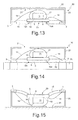
fig. 13 , the diepad 2 is etched, e.g. using a basic solution such as an ammonia solution. During etching, theterminals 3 are protected by being plated. Since thedie pad 2 is smaller than the firstadhesive film 5 and thefirst die 6, thebase region 15 is attached to the peripheral lower portion of thefirst die 6, partially through the firstadhesive film 5. In addition, as indicated above, theprotective tape 22 prevents the etchant from entering thecap 20 and from coming into contact with thedice device 50 is washed. Therefore, a package is obtained, formed by thecap 20 and thebase region 15, wherein thebase region 15 has acavity 23 extending under thedice annular portion 15A of thebase region 15 that is glued to and supports thefirst die 6. Thefirst die 6 is thus held only at the lower edge by the internalannular portion 15A of thebase region 15, to which it is firmly glued, partially with the interposition of the firstadhesive film 5. As a consequence, in this embodiment, the packageddevice 50 has an elastic, low modulus base formed bybase region 15, and no rigid metal pad region extends under thefirst die 6. - Finally,
fig. 14 , theprotective tape 22 is removed and the packageddevice 50 is bonded to a support 25, such as a printed circuit board PCB, e.g. using a solder paste (not shown). - Tests carried out by the Applicant have shown that the low
modulus base region 15 of the packageddevice 50 is very good in relieving all mechanical and thermo-mechanical stress generated during manufacturing, mounting and life of the device. In fact, thebase region 15 reliably prevents stresses generated during soldering the packageddevice 50 to the support 25 or while mounting the support 25 in place from being transferred to thesecond die 11. The same decoupling action is also ensured during operation of the packageddevice 50, since the packageddevice 50 is soldered on support 25 (SMT - surface mounted technology card), for example in case of stresses due to temperature variations. - In addition, the
base region 15 covers the ends of thebonding wires 14 welded on theterminals 3, thereby protecting them from moisture and mechanical stresses. - The
base region 15 also forms an attachment structure for thecap 20, thereby ensuring a very good tightness of the packageddevice 50. - The flexibility of the
base region 15 allows the use ofadhesive films - The damping
structure 16 offers a good protection to the packageddevice 50 also in case of fall. In fact, as shown infig. 15 , due to the quite high deformability of thebase region 15, the described packageddevice 50 has a higher flexibility with respect to pre-molded packages and thus a higher tendency to deformation in case of impacts and falls. However, in this situation, the dampingstructure 16 hits thecap 20 first and limits the movements of thedice base region 15 are also prevented bybumps 17. Thereby, thedice bonding wires 14 are not damaged. This is in particular important when thesecond die 11 is a MEMS pressure sensor having a suspended diaphragm 12 (Fig. 3 ). In particular, in tests carried out by the Applicant, it has been demonstrated that even in case of drop heights higher than 1 m against a rigid steel surface with thedevice 50 arranged upside down, thebumps 17 protect thedice device 50 remains operative and perfectly functioning, thereby complying the present norms in the automotive field in AEC-Q100-REVG May 14, 2007. The packageddevice 50 is thus reliably applicable in automotive field, for example to measure air flow (as a differential pressure device) in altimeter cockpits, or as an air flow measurement device based on differential pressure measurement, to set air conditioning flow in cockpits. - Finally, it is clear that numerous variations and modifications may be made to the described and illustrated device herein, all falling within the scope of the invention as defined in the attached claims.
- For example, the damping
structure 16 may have a different shape and/or be formed in a different position.Figs. 16 and 17 show an embodiment of a damping structure 16', where thebumps 17 are attached to aninterior face 20A of thecap 20, in a position intended to face thefirst die 6 after mounting thecap 20 to the base region 15 (as shown infig. 17 ). As an alternative, thebumps 17 may be arranged so as to face thebase region 15, laterally to thebonding wires 14, so as not to damage them when thebase region 15 deforms or bends during fall or drop. In some embodiments, thebumps 17 may be also be formed on thesecond die 11, on the die surface far from the sensing membrane area (diaphragm 12), after wire bonding, in case partially embedding the wire connections to the die. - In any case, the
bumps 17 have a height such that their distance from the cap 20 (if formed on thefirst die 6 or the base region 15) or from a facing surface (thefirst die 6 or thebase region 15, if formed on the cap 20) is lower than the distance of thebonding wires 14 from thecap 20, to protect them in case of device drop.
Claims (19)
- A surface mounting device (50) comprising at least one body (6) of semiconductor material and a package surrounding the body, the package including a base region (15) carrying the body, a cap (20) fixed to the base region and surrounding at a distance the body, contact terminals (3), and bonding wires (14) extending between the body (6) and the contact terminals (3), the bonding wires having first ends coupled to bond pads of the body (6) and second ends coupled to the contact terminals (3), the base region (15) covering the second ends of the bonding wires (14) and partially surrounding the contact terminals (3) and the lower part of the body, wherein the base region (15) has a Young's modulus lower than 5 MPa.
- A device according to claim 1, wherein the base region (15) is of an elastic or elastomeric material selected among silicone and non-silicone materials having a Young's modulus lower than 5 MPa, for example lower than 2 MPa.
- A device according to claim 1 or 2, wherein the base region (15) has a cavity (23) underlying the body (6) and an internal annular portion attached to a peripheral lower portion of the body.
- A device according to any of claims 1-3, wherein the base region (15) does not cover the upper part of the body (6) and the first ends of the bonding wires (14).
- A device according to any of claims 1-4, wherein the cap (20) is directly fixed to the base region (15).
- A device according to any of claims 1-5, further comprising a damping structure (16) extending between the cap (20) and the base region (15), the damping structure being configured to limit movement of the body (6) toward the cap.
- A device according to claim 6, wherein the damping structure (16) includes bumps (17) of an elastic material.
- A device according to any of claims 1-7, wherein the body comprises an integrated circuit die (6), a MEMS component (11), such as a pressure sensor, being mounted on the integrated circuit die (6).
- A device according to claim 8, wherein a die attach film (10) extends between the MEMS component (11) and the integrated circuit die (6).
- A device according to claim 8 or 9, wherein the device (50) further comprises bumps (17) of an elastic material extending on the sides of the MEMS component and having a height preventing the bonding wires (14) from hitting the cap (20) in case of drop of the device (50).
- A process for forming a surface mounting device, comprising:- attaching a body (6) of semiconductor material to a supporting frame (1) including contact terminals (3) separated by cavities;- connecting the body (6) to the contact terminals (3) through bonding wires (14) by bonding first ends of the bonding wires to bond pads of the body (6) and bonding second ends of the bonding wires to the contact terminals (3);- molding an elastic material having a Young's modulus lower than 5 MPa to form a base region (15) covering the second ends of the bonding wires (14) and partially surrounding the contact terminals (3) and the lower part of the body,; and- fixing a cap (20) to the base region (15) to form a package surrounding the body.
- A process according to claim 11, wherein molding an elastic material base region (15) comprises not covering the upper part of the body (6) and the first ends of the bonding wires (14) with the base region (15).
- A process according to claim 11 or 12, further comprising forming a damping structure (16) extending between the cap (20) and the base region (15) and limiting movements of the body (6) toward the cap (20).
- A process according to claim 13, wherein forming a damping structure (16) comprises dispensing elastic bumps (17) on the body (6) or the cap (20) prior to fixing the cap to the base region.
- A process according to any of claims 11-14, wherein attaching the body (6) to the supporting frame (1) comprises attaching the body to a die pad (2) of the supporting frame, the process further comprising:- after fixing the cap (20), removing the die pad (2) to form a cavity (23) in the base region (15) underlying the body (6) and exposing a back portion of the body.
- A process according to any of claims 11-15, wherein molding the base region (15) comprises dispensing and curing the elastic material.
- A process according to any of claims 11-16, wherein attaching the body (6) to the supporting frame (1) comprises applying a first adhesive film (5) between the body and the supporting frame.
- A process according to claim 17, further comprising, after attaching the body (6) to the supporting frame (1) and before molding an elastic material, attaching a MEMS component (11) onto the body (6) through a second adhesive film (19).
- A process according to claim 18, wherein the first and second adhesive films (5, 10) are die attach films.
Applications Claiming Priority (1)
| Application Number | Priority Date | Filing Date | Title |
|---|---|---|---|
| ITTO20140977 | 2014-11-26 |
Publications (2)
| Publication Number | Publication Date |
|---|---|
| EP3026696A1 true EP3026696A1 (en) | 2016-06-01 |
| EP3026696B1 EP3026696B1 (en) | 2021-03-03 |
Family
ID=52001009
Family Applications (1)
| Application Number | Title | Priority Date | Filing Date |
|---|---|---|---|
| EP15185529.3A Active EP3026696B1 (en) | 2014-11-26 | 2015-09-16 | Package for semiconductor devices sensitive to mechanical and thermo-mechanical stresses, such as mems pressure sensors |
Country Status (3)
| Country | Link |
|---|---|
| US (1) | US9841341B2 (en) |
| EP (1) | EP3026696B1 (en) |
| CN (2) | CN205257993U (en) |
Cited By (1)
| Publication number | Priority date | Publication date | Assignee | Title |
|---|---|---|---|---|
| WO2022026000A1 (en) * | 2020-07-30 | 2022-02-03 | Invensense, Inc. | Reducing delamination in a packaged integrated circuit |
Families Citing this family (8)
| Publication number | Priority date | Publication date | Assignee | Title |
|---|---|---|---|---|
| EP3026696B1 (en) | 2014-11-26 | 2021-03-03 | STMicroelectronics Srl | Package for semiconductor devices sensitive to mechanical and thermo-mechanical stresses, such as mems pressure sensors |
| US10278281B1 (en) * | 2015-10-30 | 2019-04-30 | Garmin International, Inc. | MEMS stress isolation and stabilization system |
| US9896330B2 (en) * | 2016-01-13 | 2018-02-20 | Texas Instruments Incorporated | Structure and method for packaging stress-sensitive micro-electro-mechanical system stacked onto electronic circuit chip |
| CN107539943A (en) * | 2016-06-23 | 2018-01-05 | 黄卫东 | The hybrid package structure and its method for packing of mems chip and IC chip |
| US10370244B2 (en) * | 2017-11-30 | 2019-08-06 | Infineon Technologies Ag | Deposition of protective material at wafer level in front end for early stage particle and moisture protection |
| US20190295914A1 (en) * | 2018-03-23 | 2019-09-26 | Advanced Semiconductor Engineering, Inc. | Semiconductor device package and a method of manufacturing the same |
| CN111217318A (en) | 2018-11-26 | 2020-06-02 | 罗伯特·博世有限公司 | Sensor and packaging assembly thereof |
| US20220221353A1 (en) * | 2021-01-12 | 2022-07-14 | Texas Instruments Incorporated | Semiconductor force sensors |
Citations (5)
| Publication number | Priority date | Publication date | Assignee | Title |
|---|---|---|---|---|
| US5173766A (en) * | 1990-06-25 | 1992-12-22 | Lsi Logic Corporation | Semiconductor device package and method of making such a package |
| US6309915B1 (en) * | 1998-02-05 | 2001-10-30 | Tessera, Inc. | Semiconductor chip package with expander ring and method of making same |
| US6460245B1 (en) * | 1996-03-07 | 2002-10-08 | Tessera, Inc. | Method of fabricating semiconductor chip assemblies |
| US20050056870A1 (en) * | 2002-12-19 | 2005-03-17 | Karpman Maurice S. | Stress sensitive microchip with premolded-type package |
| FR2906236A3 (en) * | 2006-09-22 | 2008-03-28 | Sigurdmicroelectronics Corp | Reinforced micro electromechanical system housing structure for e.g. computer field, has resin covering micro electromechanical system chip, control chip, wires and part of frame, and encapsulant covering resin, system chip and part |
Family Cites Families (6)
| Publication number | Priority date | Publication date | Assignee | Title |
|---|---|---|---|---|
| JP4397653B2 (en) | 2003-08-26 | 2010-01-13 | 日東電工株式会社 | Adhesive sheet for semiconductor device manufacturing |
| US8022554B2 (en) * | 2006-06-15 | 2011-09-20 | Sitime Corporation | Stacked die package for MEMS resonator system |
| ITTO20120854A1 (en) | 2012-09-28 | 2014-03-29 | Stmicroelectronics Malta Ltd | PERFORMED SURFACE MOUNTED CONTAINER FOR AN INTEGRATED SEMICONDUCTOR DEVICE, ITS ASSEMBLY AND MANUFACTURING PROCEDURE |
| US20140210019A1 (en) * | 2013-01-30 | 2014-07-31 | Invensense, Inc. | Low-cost package for integrated mems sensors |
| US8816492B1 (en) * | 2013-03-13 | 2014-08-26 | Qualtre, Inc. | Method and apparatus for isolating MEMS devices from external stimuli |
| EP3026696B1 (en) | 2014-11-26 | 2021-03-03 | STMicroelectronics Srl | Package for semiconductor devices sensitive to mechanical and thermo-mechanical stresses, such as mems pressure sensors |
-
2015
- 2015-09-16 EP EP15185529.3A patent/EP3026696B1/en active Active
- 2015-09-22 US US14/861,648 patent/US9841341B2/en active Active
- 2015-09-25 CN CN201520755154.1U patent/CN205257993U/en active Active
- 2015-09-25 CN CN201510624478.6A patent/CN105621343B/en active Active
Patent Citations (5)
| Publication number | Priority date | Publication date | Assignee | Title |
|---|---|---|---|---|
| US5173766A (en) * | 1990-06-25 | 1992-12-22 | Lsi Logic Corporation | Semiconductor device package and method of making such a package |
| US6460245B1 (en) * | 1996-03-07 | 2002-10-08 | Tessera, Inc. | Method of fabricating semiconductor chip assemblies |
| US6309915B1 (en) * | 1998-02-05 | 2001-10-30 | Tessera, Inc. | Semiconductor chip package with expander ring and method of making same |
| US20050056870A1 (en) * | 2002-12-19 | 2005-03-17 | Karpman Maurice S. | Stress sensitive microchip with premolded-type package |
| FR2906236A3 (en) * | 2006-09-22 | 2008-03-28 | Sigurdmicroelectronics Corp | Reinforced micro electromechanical system housing structure for e.g. computer field, has resin covering micro electromechanical system chip, control chip, wires and part of frame, and encapsulant covering resin, system chip and part |
Non-Patent Citations (1)
| Title |
|---|
| AEC-Q100-REVG, 14 May 2007 (2007-05-14) |
Cited By (3)
| Publication number | Priority date | Publication date | Assignee | Title |
|---|---|---|---|---|
| WO2022026000A1 (en) * | 2020-07-30 | 2022-02-03 | Invensense, Inc. | Reducing delamination in a packaged integrated circuit |
| US11584638B2 (en) | 2020-07-30 | 2023-02-21 | Invensense, Inc. | Reducing delamination in sensor package |
| TWI795761B (en) * | 2020-07-30 | 2023-03-11 | 美商伊凡聖斯股份有限公司 | Reducing delamination in sensor package and method thereof |
Also Published As
| Publication number | Publication date |
|---|---|
| CN105621343A (en) | 2016-06-01 |
| CN205257993U (en) | 2016-05-25 |
| CN105621343B (en) | 2018-05-11 |
| US9841341B2 (en) | 2017-12-12 |
| EP3026696B1 (en) | 2021-03-03 |
| US20160146692A1 (en) | 2016-05-26 |
Similar Documents
| Publication | Publication Date | Title |
|---|---|---|
| EP3026696B1 (en) | Package for semiconductor devices sensitive to mechanical and thermo-mechanical stresses, such as mems pressure sensors | |
| US7282786B2 (en) | Semiconductor package and process for making the same | |
| US7568390B2 (en) | Semiconductor acceleration sensor device and method for manufacturing the same | |
| US7571647B2 (en) | Package structure for an acceleration sensor | |
| US9656856B2 (en) | Method of lower profile MEMS package with stress isolations | |
| US20140374848A1 (en) | Semiconductor sensor device with metal lid | |
| US20120133042A1 (en) | Mounting structure of chip and module using the same | |
| US20170110416A1 (en) | Chip package having a protection piece compliantly attached on a chip sensing surface | |
| US9029999B2 (en) | Semiconductor sensor device with footed lid | |
| US10800651B2 (en) | Low stress integrated device packages | |
| US9297713B2 (en) | Pressure sensor device with through silicon via | |
| US9054089B2 (en) | Lead frame package having discharge holes and method of manufacturing the same | |
| US9890034B2 (en) | Cavity type pressure sensor device | |
| JP4925832B2 (en) | Method for mounting an optical sensor | |
| US20070257345A1 (en) | Package structure to reduce warpage | |
| US20150035130A1 (en) | Integrated Circuit with Stress Isolation | |
| US9099363B1 (en) | Substrate with corner cut-outs and semiconductor device assembled therewith | |
| JP6317956B2 (en) | Pressure sensor and method of manufacturing pressure sensor | |
| KR20110076539A (en) | Pressure sensor and manufacture method thereof | |
| KR101688077B1 (en) | Semiconductor package structure and manufacturing method thereof | |
| CN111033704B (en) | Integrated circuit package with stress directing material | |
| WO2011099356A1 (en) | Package component | |
| CN112885789A (en) | Flexible pneumatic pressure measuring device and manufacturing method thereof | |
| KR20080064798A (en) | Acceleration sensor | |
| KR20080074656A (en) | Semiconductor package |
Legal Events
| Date | Code | Title | Description |
|---|---|---|---|
| PUAI | Public reference made under article 153(3) epc to a published international application that has entered the european phase |
Free format text: ORIGINAL CODE: 0009012 |
|
| AK | Designated contracting states |
Kind code of ref document: A1 Designated state(s): AL AT BE BG CH CY CZ DE DK EE ES FI FR GB GR HR HU IE IS IT LI LT LU LV MC MK MT NL NO PL PT RO RS SE SI SK SM TR |
|
| AX | Request for extension of the european patent |
Extension state: BA ME |
|
| STAA | Information on the status of an ep patent application or granted ep patent |
Free format text: STATUS: REQUEST FOR EXAMINATION WAS MADE |
|
| 17P | Request for examination filed |
Effective date: 20161130 |
|
| RBV | Designated contracting states (corrected) |
Designated state(s): AL AT BE BG CH CY CZ DE DK EE ES FI FR GB GR HR HU IE IS IT LI LT LU LV MC MK MT NL NO PL PT RO RS SE SI SK SM TR |
|
| STAA | Information on the status of an ep patent application or granted ep patent |
Free format text: STATUS: EXAMINATION IS IN PROGRESS |
|
| 17Q | First examination report despatched |
Effective date: 20200226 |
|
| GRAP | Despatch of communication of intention to grant a patent |
Free format text: ORIGINAL CODE: EPIDOSNIGR1 |
|
| STAA | Information on the status of an ep patent application or granted ep patent |
Free format text: STATUS: GRANT OF PATENT IS INTENDED |
|
| INTG | Intention to grant announced |
Effective date: 20200921 |
|
| GRAS | Grant fee paid |
Free format text: ORIGINAL CODE: EPIDOSNIGR3 |
|
| STAA | Information on the status of an ep patent application or granted ep patent |
Free format text: STATUS: GRANT OF PATENT IS INTENDED |
|
| GRAA | (expected) grant |
Free format text: ORIGINAL CODE: 0009210 |
|
| STAA | Information on the status of an ep patent application or granted ep patent |
Free format text: STATUS: THE PATENT HAS BEEN GRANTED |
|
| AK | Designated contracting states |
Kind code of ref document: B1 Designated state(s): AL AT BE BG CH CY CZ DE DK EE ES FI FR GB GR HR HU IE IS IT LI LT LU LV MC MK MT NL NO PL PT RO RS SE SI SK SM TR |
|
| REG | Reference to a national code |
Ref country code: GB Ref legal event code: FG4D |
|
| REG | Reference to a national code |
Ref country code: AT Ref legal event code: REF Ref document number: 1368132 Country of ref document: AT Kind code of ref document: T Effective date: 20210315 Ref country code: CH Ref legal event code: EP |
|
| REG | Reference to a national code |
Ref country code: DE Ref legal event code: R096 Ref document number: 602015066264 Country of ref document: DE |
|
| REG | Reference to a national code |
Ref country code: IE Ref legal event code: FG4D |
|
| REG | Reference to a national code |
Ref country code: LT Ref legal event code: MG9D |
|
| PG25 | Lapsed in a contracting state [announced via postgrant information from national office to epo] |
Ref country code: LT Free format text: LAPSE BECAUSE OF FAILURE TO SUBMIT A TRANSLATION OF THE DESCRIPTION OR TO PAY THE FEE WITHIN THE PRESCRIBED TIME-LIMIT Effective date: 20210303 Ref country code: FI Free format text: LAPSE BECAUSE OF FAILURE TO SUBMIT A TRANSLATION OF THE DESCRIPTION OR TO PAY THE FEE WITHIN THE PRESCRIBED TIME-LIMIT Effective date: 20210303 Ref country code: HR Free format text: LAPSE BECAUSE OF FAILURE TO SUBMIT A TRANSLATION OF THE DESCRIPTION OR TO PAY THE FEE WITHIN THE PRESCRIBED TIME-LIMIT Effective date: 20210303 Ref country code: GR Free format text: LAPSE BECAUSE OF FAILURE TO SUBMIT A TRANSLATION OF THE DESCRIPTION OR TO PAY THE FEE WITHIN THE PRESCRIBED TIME-LIMIT Effective date: 20210604 Ref country code: NO Free format text: LAPSE BECAUSE OF FAILURE TO SUBMIT A TRANSLATION OF THE DESCRIPTION OR TO PAY THE FEE WITHIN THE PRESCRIBED TIME-LIMIT Effective date: 20210603 Ref country code: BG Free format text: LAPSE BECAUSE OF FAILURE TO SUBMIT A TRANSLATION OF THE DESCRIPTION OR TO PAY THE FEE WITHIN THE PRESCRIBED TIME-LIMIT Effective date: 20210603 |
|
| REG | Reference to a national code |
Ref country code: NL Ref legal event code: MP Effective date: 20210303 |
|
| REG | Reference to a national code |
Ref country code: AT Ref legal event code: MK05 Ref document number: 1368132 Country of ref document: AT Kind code of ref document: T Effective date: 20210303 |
|
| PG25 | Lapsed in a contracting state [announced via postgrant information from national office to epo] |
Ref country code: LV Free format text: LAPSE BECAUSE OF FAILURE TO SUBMIT A TRANSLATION OF THE DESCRIPTION OR TO PAY THE FEE WITHIN THE PRESCRIBED TIME-LIMIT Effective date: 20210303 Ref country code: RS Free format text: LAPSE BECAUSE OF FAILURE TO SUBMIT A TRANSLATION OF THE DESCRIPTION OR TO PAY THE FEE WITHIN THE PRESCRIBED TIME-LIMIT Effective date: 20210303 Ref country code: PL Free format text: LAPSE BECAUSE OF FAILURE TO SUBMIT A TRANSLATION OF THE DESCRIPTION OR TO PAY THE FEE WITHIN THE PRESCRIBED TIME-LIMIT Effective date: 20210303 Ref country code: SE Free format text: LAPSE BECAUSE OF FAILURE TO SUBMIT A TRANSLATION OF THE DESCRIPTION OR TO PAY THE FEE WITHIN THE PRESCRIBED TIME-LIMIT Effective date: 20210303 |
|
| PG25 | Lapsed in a contracting state [announced via postgrant information from national office to epo] |
Ref country code: NL Free format text: LAPSE BECAUSE OF FAILURE TO SUBMIT A TRANSLATION OF THE DESCRIPTION OR TO PAY THE FEE WITHIN THE PRESCRIBED TIME-LIMIT Effective date: 20210303 |
|
| PG25 | Lapsed in a contracting state [announced via postgrant information from national office to epo] |
Ref country code: SM Free format text: LAPSE BECAUSE OF FAILURE TO SUBMIT A TRANSLATION OF THE DESCRIPTION OR TO PAY THE FEE WITHIN THE PRESCRIBED TIME-LIMIT Effective date: 20210303 Ref country code: CZ Free format text: LAPSE BECAUSE OF FAILURE TO SUBMIT A TRANSLATION OF THE DESCRIPTION OR TO PAY THE FEE WITHIN THE PRESCRIBED TIME-LIMIT Effective date: 20210303 Ref country code: EE Free format text: LAPSE BECAUSE OF FAILURE TO SUBMIT A TRANSLATION OF THE DESCRIPTION OR TO PAY THE FEE WITHIN THE PRESCRIBED TIME-LIMIT Effective date: 20210303 Ref country code: AT Free format text: LAPSE BECAUSE OF FAILURE TO SUBMIT A TRANSLATION OF THE DESCRIPTION OR TO PAY THE FEE WITHIN THE PRESCRIBED TIME-LIMIT Effective date: 20210303 |
|
| PG25 | Lapsed in a contracting state [announced via postgrant information from national office to epo] |
Ref country code: IS Free format text: LAPSE BECAUSE OF FAILURE TO SUBMIT A TRANSLATION OF THE DESCRIPTION OR TO PAY THE FEE WITHIN THE PRESCRIBED TIME-LIMIT Effective date: 20210703 Ref country code: PT Free format text: LAPSE BECAUSE OF FAILURE TO SUBMIT A TRANSLATION OF THE DESCRIPTION OR TO PAY THE FEE WITHIN THE PRESCRIBED TIME-LIMIT Effective date: 20210705 Ref country code: ES Free format text: LAPSE BECAUSE OF FAILURE TO SUBMIT A TRANSLATION OF THE DESCRIPTION OR TO PAY THE FEE WITHIN THE PRESCRIBED TIME-LIMIT Effective date: 20210303 Ref country code: SK Free format text: LAPSE BECAUSE OF FAILURE TO SUBMIT A TRANSLATION OF THE DESCRIPTION OR TO PAY THE FEE WITHIN THE PRESCRIBED TIME-LIMIT Effective date: 20210303 Ref country code: RO Free format text: LAPSE BECAUSE OF FAILURE TO SUBMIT A TRANSLATION OF THE DESCRIPTION OR TO PAY THE FEE WITHIN THE PRESCRIBED TIME-LIMIT Effective date: 20210303 |
|
| REG | Reference to a national code |
Ref country code: DE Ref legal event code: R097 Ref document number: 602015066264 Country of ref document: DE |
|
| PLBE | No opposition filed within time limit |
Free format text: ORIGINAL CODE: 0009261 |
|
| STAA | Information on the status of an ep patent application or granted ep patent |
Free format text: STATUS: NO OPPOSITION FILED WITHIN TIME LIMIT |
|
| PG25 | Lapsed in a contracting state [announced via postgrant information from national office to epo] |
Ref country code: DK Free format text: LAPSE BECAUSE OF FAILURE TO SUBMIT A TRANSLATION OF THE DESCRIPTION OR TO PAY THE FEE WITHIN THE PRESCRIBED TIME-LIMIT Effective date: 20210303 Ref country code: AL Free format text: LAPSE BECAUSE OF FAILURE TO SUBMIT A TRANSLATION OF THE DESCRIPTION OR TO PAY THE FEE WITHIN THE PRESCRIBED TIME-LIMIT Effective date: 20210303 |
|
| 26N | No opposition filed |
Effective date: 20211206 |
|
| PG25 | Lapsed in a contracting state [announced via postgrant information from national office to epo] |
Ref country code: SI Free format text: LAPSE BECAUSE OF FAILURE TO SUBMIT A TRANSLATION OF THE DESCRIPTION OR TO PAY THE FEE WITHIN THE PRESCRIBED TIME-LIMIT Effective date: 20210303 |
|
| PG25 | Lapsed in a contracting state [announced via postgrant information from national office to epo] |
Ref country code: IT Free format text: LAPSE BECAUSE OF FAILURE TO SUBMIT A TRANSLATION OF THE DESCRIPTION OR TO PAY THE FEE WITHIN THE PRESCRIBED TIME-LIMIT Effective date: 20210303 |
|
| REG | Reference to a national code |
Ref country code: CH Ref legal event code: PL |
|
| REG | Reference to a national code |
Ref country code: BE Ref legal event code: MM Effective date: 20210930 |
|
| GBPC | Gb: european patent ceased through non-payment of renewal fee |
Effective date: 20210916 |
|
| PG25 | Lapsed in a contracting state [announced via postgrant information from national office to epo] |
Ref country code: IS Free format text: LAPSE BECAUSE OF FAILURE TO SUBMIT A TRANSLATION OF THE DESCRIPTION OR TO PAY THE FEE WITHIN THE PRESCRIBED TIME-LIMIT Effective date: 20210703 Ref country code: MC Free format text: LAPSE BECAUSE OF FAILURE TO SUBMIT A TRANSLATION OF THE DESCRIPTION OR TO PAY THE FEE WITHIN THE PRESCRIBED TIME-LIMIT Effective date: 20210303 |
|
| PG25 | Lapsed in a contracting state [announced via postgrant information from national office to epo] |
Ref country code: LU Free format text: LAPSE BECAUSE OF NON-PAYMENT OF DUE FEES Effective date: 20210916 Ref country code: IE Free format text: LAPSE BECAUSE OF NON-PAYMENT OF DUE FEES Effective date: 20210916 Ref country code: GB Free format text: LAPSE BECAUSE OF NON-PAYMENT OF DUE FEES Effective date: 20210916 Ref country code: FR Free format text: LAPSE BECAUSE OF NON-PAYMENT OF DUE FEES Effective date: 20210930 Ref country code: BE Free format text: LAPSE BECAUSE OF NON-PAYMENT OF DUE FEES Effective date: 20210930 |
|
| PG25 | Lapsed in a contracting state [announced via postgrant information from national office to epo] |
Ref country code: LI Free format text: LAPSE BECAUSE OF NON-PAYMENT OF DUE FEES Effective date: 20210930 Ref country code: CH Free format text: LAPSE BECAUSE OF NON-PAYMENT OF DUE FEES Effective date: 20210930 |
|
| REG | Reference to a national code |
Ref country code: DE Ref legal event code: R081 Ref document number: 602015066264 Country of ref document: DE Owner name: STMICROELECTRONICS INTERNATIONAL N.V., CH Free format text: FORMER OWNERS: STMICROELECTRONICS, INC., CALAMBA CITY, LAGUNA, PH; STMICROELECTRONICS S.R.L., AGRATE BRIANZA, MONZA E BRIANZA, IT |
|
| PG25 | Lapsed in a contracting state [announced via postgrant information from national office to epo] |
Ref country code: HU Free format text: LAPSE BECAUSE OF FAILURE TO SUBMIT A TRANSLATION OF THE DESCRIPTION OR TO PAY THE FEE WITHIN THE PRESCRIBED TIME-LIMIT; INVALID AB INITIO Effective date: 20150916 |
|
| PG25 | Lapsed in a contracting state [announced via postgrant information from national office to epo] |
Ref country code: CY Free format text: LAPSE BECAUSE OF FAILURE TO SUBMIT A TRANSLATION OF THE DESCRIPTION OR TO PAY THE FEE WITHIN THE PRESCRIBED TIME-LIMIT Effective date: 20210303 |
|
| PGFP | Annual fee paid to national office [announced via postgrant information from national office to epo] |
Ref country code: DE Payment date: 20230822 Year of fee payment: 9 |