EP3025192B1 - Electrochromic devices having improved structure for reducing current leakage across portions of the lower transparent conductor layer - Google Patents
Electrochromic devices having improved structure for reducing current leakage across portions of the lower transparent conductor layer Download PDFInfo
- Publication number
- EP3025192B1 EP3025192B1 EP14755454.7A EP14755454A EP3025192B1 EP 3025192 B1 EP3025192 B1 EP 3025192B1 EP 14755454 A EP14755454 A EP 14755454A EP 3025192 B1 EP3025192 B1 EP 3025192B1
- Authority
- EP
- European Patent Office
- Prior art keywords
- layer
- conductive layer
- transparent conductive
- lower transparent
- electrode
- Prior art date
- Legal status (The legal status is an assumption and is not a legal conclusion. Google has not performed a legal analysis and makes no representation as to the accuracy of the status listed.)
- Active
Links
- 239000004020 conductor Substances 0.000 title description 14
- 238000000034 method Methods 0.000 claims description 35
- 150000002500 ions Chemical class 0.000 claims description 32
- 239000010416 ion conductor Substances 0.000 claims description 29
- 238000000151 deposition Methods 0.000 claims description 23
- 238000005520 cutting process Methods 0.000 claims description 11
- USPVIMZDBBWXGM-UHFFFAOYSA-N nickel;oxotungsten Chemical compound [Ni].[W]=O USPVIMZDBBWXGM-UHFFFAOYSA-N 0.000 claims description 8
- 238000004891 communication Methods 0.000 claims description 4
- 238000002360 preparation method Methods 0.000 claims description 3
- 230000003287 optical effect Effects 0.000 description 20
- 239000000463 material Substances 0.000 description 18
- 229910052744 lithium Inorganic materials 0.000 description 14
- 239000010408 film Substances 0.000 description 13
- WHXSMMKQMYFTQS-UHFFFAOYSA-N Lithium Chemical compound [Li] WHXSMMKQMYFTQS-UHFFFAOYSA-N 0.000 description 12
- 239000000758 substrate Substances 0.000 description 12
- 238000004544 sputter deposition Methods 0.000 description 11
- 229910001416 lithium ion Inorganic materials 0.000 description 10
- 230000005012 migration Effects 0.000 description 10
- 238000013508 migration Methods 0.000 description 10
- 230000008569 process Effects 0.000 description 10
- HBBGRARXTFLTSG-UHFFFAOYSA-N Lithium ion Chemical compound [Li+] HBBGRARXTFLTSG-UHFFFAOYSA-N 0.000 description 9
- 230000008021 deposition Effects 0.000 description 9
- 238000000576 coating method Methods 0.000 description 7
- 239000011521 glass Substances 0.000 description 7
- 239000011248 coating agent Substances 0.000 description 5
- 238000010586 diagram Methods 0.000 description 5
- 238000012545 processing Methods 0.000 description 5
- 238000005546 reactive sputtering Methods 0.000 description 5
- 230000005540 biological transmission Effects 0.000 description 4
- 238000001755 magnetron sputter deposition Methods 0.000 description 4
- 238000004519 manufacturing process Methods 0.000 description 4
- 230000007704 transition Effects 0.000 description 4
- 230000000903 blocking effect Effects 0.000 description 3
- 238000005137 deposition process Methods 0.000 description 3
- 238000003780 insertion Methods 0.000 description 3
- 230000037431 insertion Effects 0.000 description 3
- -1 lithium aluminum fluoride Chemical compound 0.000 description 3
- 230000009467 reduction Effects 0.000 description 3
- VYPSYNLAJGMNEJ-UHFFFAOYSA-N Silicium dioxide Chemical compound O=[Si]=O VYPSYNLAJGMNEJ-UHFFFAOYSA-N 0.000 description 2
- 230000015572 biosynthetic process Effects 0.000 description 2
- 238000005229 chemical vapour deposition Methods 0.000 description 2
- 230000000295 complement effect Effects 0.000 description 2
- 238000009792 diffusion process Methods 0.000 description 2
- 230000000694 effects Effects 0.000 description 2
- 230000005684 electric field Effects 0.000 description 2
- 238000005530 etching Methods 0.000 description 2
- 238000001704 evaporation Methods 0.000 description 2
- 230000008020 evaporation Effects 0.000 description 2
- 238000010438 heat treatment Methods 0.000 description 2
- 238000009830 intercalation Methods 0.000 description 2
- 230000002687 intercalation Effects 0.000 description 2
- 238000000608 laser ablation Methods 0.000 description 2
- 238000005240 physical vapour deposition Methods 0.000 description 2
- 230000002441 reversible effect Effects 0.000 description 2
- 229910001415 sodium ion Inorganic materials 0.000 description 2
- 239000000126 substance Substances 0.000 description 2
- 239000010409 thin film Substances 0.000 description 2
- BPQQTUXANYXVAA-UHFFFAOYSA-N Orthosilicate Chemical compound [O-][Si]([O-])([O-])[O-] BPQQTUXANYXVAA-UHFFFAOYSA-N 0.000 description 1
- JFBZPFYRPYOZCQ-UHFFFAOYSA-N [Li].[Al] Chemical compound [Li].[Al] JFBZPFYRPYOZCQ-UHFFFAOYSA-N 0.000 description 1
- YJSAVIWBELEHDD-UHFFFAOYSA-N [Li].[Si]=O Chemical compound [Li].[Si]=O YJSAVIWBELEHDD-UHFFFAOYSA-N 0.000 description 1
- LFZYLAXEYRJERI-UHFFFAOYSA-N [Li].[Zr] Chemical compound [Li].[Zr] LFZYLAXEYRJERI-UHFFFAOYSA-N 0.000 description 1
- 238000005299 abrasion Methods 0.000 description 1
- 238000010521 absorption reaction Methods 0.000 description 1
- PGTAKMRAYVRICI-UHFFFAOYSA-N aluminum lithium borate Chemical compound B([O-])([O-])[O-].[Al+3].[Li+] PGTAKMRAYVRICI-UHFFFAOYSA-N 0.000 description 1
- 239000007844 bleaching agent Substances 0.000 description 1
- 230000015556 catabolic process Effects 0.000 description 1
- 229910010293 ceramic material Inorganic materials 0.000 description 1
- 230000008859 change Effects 0.000 description 1
- 238000003486 chemical etching Methods 0.000 description 1
- 238000004040 coloring Methods 0.000 description 1
- 239000002131 composite material Substances 0.000 description 1
- 230000001351 cycling effect Effects 0.000 description 1
- 238000000354 decomposition reaction Methods 0.000 description 1
- 230000007547 defect Effects 0.000 description 1
- 230000001419 dependent effect Effects 0.000 description 1
- 229910003460 diamond Inorganic materials 0.000 description 1
- 239000010432 diamond Substances 0.000 description 1
- 238000003618 dip coating Methods 0.000 description 1
- 239000000428 dust Substances 0.000 description 1
- 238000009760 electrical discharge machining Methods 0.000 description 1
- 239000006181 electrochemical material Substances 0.000 description 1
- 238000004070 electrodeposition Methods 0.000 description 1
- 239000003792 electrolyte Substances 0.000 description 1
- 238000006056 electrooxidation reaction Methods 0.000 description 1
- 238000000605 extraction Methods 0.000 description 1
- XGZVUEUWXADBQD-UHFFFAOYSA-L lithium carbonate Chemical compound [Li+].[Li+].[O-]C([O-])=O XGZVUEUWXADBQD-UHFFFAOYSA-L 0.000 description 1
- 229910052808 lithium carbonate Inorganic materials 0.000 description 1
- PAZHGORSDKKUPI-UHFFFAOYSA-N lithium metasilicate Chemical compound [Li+].[Li+].[O-][Si]([O-])=O PAZHGORSDKKUPI-UHFFFAOYSA-N 0.000 description 1
- GQYHUHYESMUTHG-UHFFFAOYSA-N lithium niobate Chemical compound [Li+].[O-][Nb](=O)=O GQYHUHYESMUTHG-UHFFFAOYSA-N 0.000 description 1
- IDBFBDSKYCUNPW-UHFFFAOYSA-N lithium nitride Chemical compound [Li]N([Li])[Li] IDBFBDSKYCUNPW-UHFFFAOYSA-N 0.000 description 1
- FUJCRWPEOMXPAD-UHFFFAOYSA-N lithium oxide Chemical compound [Li+].[Li+].[O-2] FUJCRWPEOMXPAD-UHFFFAOYSA-N 0.000 description 1
- 229910001947 lithium oxide Inorganic materials 0.000 description 1
- 229910052912 lithium silicate Inorganic materials 0.000 description 1
- 230000000873 masking effect Effects 0.000 description 1
- 229910052751 metal Inorganic materials 0.000 description 1
- 239000002184 metal Substances 0.000 description 1
- 239000000203 mixture Substances 0.000 description 1
- 238000012986 modification Methods 0.000 description 1
- 230000004048 modification Effects 0.000 description 1
- 230000003647 oxidation Effects 0.000 description 1
- 238000007254 oxidation reaction Methods 0.000 description 1
- BPUBBGLMJRNUCC-UHFFFAOYSA-N oxygen(2-);tantalum(5+) Chemical compound [O-2].[O-2].[O-2].[O-2].[O-2].[Ta+5].[Ta+5] BPUBBGLMJRNUCC-UHFFFAOYSA-N 0.000 description 1
- 238000000059 patterning Methods 0.000 description 1
- 230000008092 positive effect Effects 0.000 description 1
- 238000001552 radio frequency sputter deposition Methods 0.000 description 1
- 230000004044 response Effects 0.000 description 1
- 239000010979 ruby Substances 0.000 description 1
- 229910001750 ruby Inorganic materials 0.000 description 1
- 235000012239 silicon dioxide Nutrition 0.000 description 1
- 239000000377 silicon dioxide Substances 0.000 description 1
- LIVNPJMFVYWSIS-UHFFFAOYSA-N silicon monoxide Chemical class [Si-]#[O+] LIVNPJMFVYWSIS-UHFFFAOYSA-N 0.000 description 1
- 229910052814 silicon oxide Inorganic materials 0.000 description 1
- 238000003980 solgel method Methods 0.000 description 1
- 239000007784 solid electrolyte Substances 0.000 description 1
- 238000004528 spin coating Methods 0.000 description 1
- 238000005118 spray pyrolysis Methods 0.000 description 1
- 238000005507 spraying Methods 0.000 description 1
- 229910001220 stainless steel Inorganic materials 0.000 description 1
- 239000010935 stainless steel Substances 0.000 description 1
- 238000003860 storage Methods 0.000 description 1
- 229910001936 tantalum oxide Inorganic materials 0.000 description 1
- 238000007736 thin film deposition technique Methods 0.000 description 1
- 238000002834 transmittance Methods 0.000 description 1
- RIUWBIIVUYSTCN-UHFFFAOYSA-N trilithium borate Chemical compound [Li+].[Li+].[Li+].[O-]B([O-])[O-] RIUWBIIVUYSTCN-UHFFFAOYSA-N 0.000 description 1
- 238000013022 venting Methods 0.000 description 1
Images


Classifications
-
- G—PHYSICS
- G02—OPTICS
- G02F—OPTICAL DEVICES OR ARRANGEMENTS FOR THE CONTROL OF LIGHT BY MODIFICATION OF THE OPTICAL PROPERTIES OF THE MEDIA OF THE ELEMENTS INVOLVED THEREIN; NON-LINEAR OPTICS; FREQUENCY-CHANGING OF LIGHT; OPTICAL LOGIC ELEMENTS; OPTICAL ANALOGUE/DIGITAL CONVERTERS
- G02F1/00—Devices or arrangements for the control of the intensity, colour, phase, polarisation or direction of light arriving from an independent light source, e.g. switching, gating or modulating; Non-linear optics
- G02F1/01—Devices or arrangements for the control of the intensity, colour, phase, polarisation or direction of light arriving from an independent light source, e.g. switching, gating or modulating; Non-linear optics for the control of the intensity, phase, polarisation or colour
- G02F1/15—Devices or arrangements for the control of the intensity, colour, phase, polarisation or direction of light arriving from an independent light source, e.g. switching, gating or modulating; Non-linear optics for the control of the intensity, phase, polarisation or colour based on an electrochromic effect
- G02F1/153—Constructional details
- G02F1/155—Electrodes
-
- G—PHYSICS
- G02—OPTICS
- G02F—OPTICAL DEVICES OR ARRANGEMENTS FOR THE CONTROL OF LIGHT BY MODIFICATION OF THE OPTICAL PROPERTIES OF THE MEDIA OF THE ELEMENTS INVOLVED THEREIN; NON-LINEAR OPTICS; FREQUENCY-CHANGING OF LIGHT; OPTICAL LOGIC ELEMENTS; OPTICAL ANALOGUE/DIGITAL CONVERTERS
- G02F1/00—Devices or arrangements for the control of the intensity, colour, phase, polarisation or direction of light arriving from an independent light source, e.g. switching, gating or modulating; Non-linear optics
- G02F1/0009—Materials therefor
- G02F1/0018—Electro-optical materials
-
- G—PHYSICS
- G02—OPTICS
- G02F—OPTICAL DEVICES OR ARRANGEMENTS FOR THE CONTROL OF LIGHT BY MODIFICATION OF THE OPTICAL PROPERTIES OF THE MEDIA OF THE ELEMENTS INVOLVED THEREIN; NON-LINEAR OPTICS; FREQUENCY-CHANGING OF LIGHT; OPTICAL LOGIC ELEMENTS; OPTICAL ANALOGUE/DIGITAL CONVERTERS
- G02F1/00—Devices or arrangements for the control of the intensity, colour, phase, polarisation or direction of light arriving from an independent light source, e.g. switching, gating or modulating; Non-linear optics
- G02F1/01—Devices or arrangements for the control of the intensity, colour, phase, polarisation or direction of light arriving from an independent light source, e.g. switching, gating or modulating; Non-linear optics for the control of the intensity, phase, polarisation or colour
- G02F1/0102—Constructional details, not otherwise provided for in this subclass
- G02F1/0107—Gaskets, spacers or sealing of cells; Filling and closing of cells
-
- G—PHYSICS
- G02—OPTICS
- G02F—OPTICAL DEVICES OR ARRANGEMENTS FOR THE CONTROL OF LIGHT BY MODIFICATION OF THE OPTICAL PROPERTIES OF THE MEDIA OF THE ELEMENTS INVOLVED THEREIN; NON-LINEAR OPTICS; FREQUENCY-CHANGING OF LIGHT; OPTICAL LOGIC ELEMENTS; OPTICAL ANALOGUE/DIGITAL CONVERTERS
- G02F1/00—Devices or arrangements for the control of the intensity, colour, phase, polarisation or direction of light arriving from an independent light source, e.g. switching, gating or modulating; Non-linear optics
- G02F1/01—Devices or arrangements for the control of the intensity, colour, phase, polarisation or direction of light arriving from an independent light source, e.g. switching, gating or modulating; Non-linear optics for the control of the intensity, phase, polarisation or colour
- G02F1/13—Devices or arrangements for the control of the intensity, colour, phase, polarisation or direction of light arriving from an independent light source, e.g. switching, gating or modulating; Non-linear optics for the control of the intensity, phase, polarisation or colour based on liquid crystals, e.g. single liquid crystal display cells
- G02F1/133—Constructional arrangements; Operation of liquid crystal cells; Circuit arrangements
- G02F1/1333—Constructional arrangements; Manufacturing methods
- G02F1/133305—Flexible substrates, e.g. plastics, organic film
-
- G—PHYSICS
- G02—OPTICS
- G02F—OPTICAL DEVICES OR ARRANGEMENTS FOR THE CONTROL OF LIGHT BY MODIFICATION OF THE OPTICAL PROPERTIES OF THE MEDIA OF THE ELEMENTS INVOLVED THEREIN; NON-LINEAR OPTICS; FREQUENCY-CHANGING OF LIGHT; OPTICAL LOGIC ELEMENTS; OPTICAL ANALOGUE/DIGITAL CONVERTERS
- G02F1/00—Devices or arrangements for the control of the intensity, colour, phase, polarisation or direction of light arriving from an independent light source, e.g. switching, gating or modulating; Non-linear optics
- G02F1/01—Devices or arrangements for the control of the intensity, colour, phase, polarisation or direction of light arriving from an independent light source, e.g. switching, gating or modulating; Non-linear optics for the control of the intensity, phase, polarisation or colour
- G02F1/13—Devices or arrangements for the control of the intensity, colour, phase, polarisation or direction of light arriving from an independent light source, e.g. switching, gating or modulating; Non-linear optics for the control of the intensity, phase, polarisation or colour based on liquid crystals, e.g. single liquid crystal display cells
- G02F1/133—Constructional arrangements; Operation of liquid crystal cells; Circuit arrangements
- G02F1/1333—Constructional arrangements; Manufacturing methods
- G02F1/1339—Gaskets; Spacers; Sealing of cells
-
- G—PHYSICS
- G02—OPTICS
- G02F—OPTICAL DEVICES OR ARRANGEMENTS FOR THE CONTROL OF LIGHT BY MODIFICATION OF THE OPTICAL PROPERTIES OF THE MEDIA OF THE ELEMENTS INVOLVED THEREIN; NON-LINEAR OPTICS; FREQUENCY-CHANGING OF LIGHT; OPTICAL LOGIC ELEMENTS; OPTICAL ANALOGUE/DIGITAL CONVERTERS
- G02F1/00—Devices or arrangements for the control of the intensity, colour, phase, polarisation or direction of light arriving from an independent light source, e.g. switching, gating or modulating; Non-linear optics
- G02F1/01—Devices or arrangements for the control of the intensity, colour, phase, polarisation or direction of light arriving from an independent light source, e.g. switching, gating or modulating; Non-linear optics for the control of the intensity, phase, polarisation or colour
- G02F1/15—Devices or arrangements for the control of the intensity, colour, phase, polarisation or direction of light arriving from an independent light source, e.g. switching, gating or modulating; Non-linear optics for the control of the intensity, phase, polarisation or colour based on an electrochromic effect
- G02F1/1506—Devices or arrangements for the control of the intensity, colour, phase, polarisation or direction of light arriving from an independent light source, e.g. switching, gating or modulating; Non-linear optics for the control of the intensity, phase, polarisation or colour based on an electrochromic effect caused by electrodeposition, e.g. electrolytic deposition of an inorganic material on or close to an electrode
- G02F1/1508—Devices or arrangements for the control of the intensity, colour, phase, polarisation or direction of light arriving from an independent light source, e.g. switching, gating or modulating; Non-linear optics for the control of the intensity, phase, polarisation or colour based on an electrochromic effect caused by electrodeposition, e.g. electrolytic deposition of an inorganic material on or close to an electrode using a solid electrolyte
-
- G—PHYSICS
- G02—OPTICS
- G02F—OPTICAL DEVICES OR ARRANGEMENTS FOR THE CONTROL OF LIGHT BY MODIFICATION OF THE OPTICAL PROPERTIES OF THE MEDIA OF THE ELEMENTS INVOLVED THEREIN; NON-LINEAR OPTICS; FREQUENCY-CHANGING OF LIGHT; OPTICAL LOGIC ELEMENTS; OPTICAL ANALOGUE/DIGITAL CONVERTERS
- G02F1/00—Devices or arrangements for the control of the intensity, colour, phase, polarisation or direction of light arriving from an independent light source, e.g. switching, gating or modulating; Non-linear optics
- G02F1/01—Devices or arrangements for the control of the intensity, colour, phase, polarisation or direction of light arriving from an independent light source, e.g. switching, gating or modulating; Non-linear optics for the control of the intensity, phase, polarisation or colour
- G02F1/15—Devices or arrangements for the control of the intensity, colour, phase, polarisation or direction of light arriving from an independent light source, e.g. switching, gating or modulating; Non-linear optics for the control of the intensity, phase, polarisation or colour based on an electrochromic effect
- G02F1/153—Constructional details
- G02F1/1533—Constructional details structural features not otherwise provided for
-
- G—PHYSICS
- G02—OPTICS
- G02F—OPTICAL DEVICES OR ARRANGEMENTS FOR THE CONTROL OF LIGHT BY MODIFICATION OF THE OPTICAL PROPERTIES OF THE MEDIA OF THE ELEMENTS INVOLVED THEREIN; NON-LINEAR OPTICS; FREQUENCY-CHANGING OF LIGHT; OPTICAL LOGIC ELEMENTS; OPTICAL ANALOGUE/DIGITAL CONVERTERS
- G02F1/00—Devices or arrangements for the control of the intensity, colour, phase, polarisation or direction of light arriving from an independent light source, e.g. switching, gating or modulating; Non-linear optics
- G02F1/01—Devices or arrangements for the control of the intensity, colour, phase, polarisation or direction of light arriving from an independent light source, e.g. switching, gating or modulating; Non-linear optics for the control of the intensity, phase, polarisation or colour
- G02F1/15—Devices or arrangements for the control of the intensity, colour, phase, polarisation or direction of light arriving from an independent light source, e.g. switching, gating or modulating; Non-linear optics for the control of the intensity, phase, polarisation or colour based on an electrochromic effect
- G02F1/153—Constructional details
- G02F1/157—Structural association of cells with optical devices, e.g. reflectors or illuminating devices
-
- G—PHYSICS
- G02—OPTICS
- G02F—OPTICAL DEVICES OR ARRANGEMENTS FOR THE CONTROL OF LIGHT BY MODIFICATION OF THE OPTICAL PROPERTIES OF THE MEDIA OF THE ELEMENTS INVOLVED THEREIN; NON-LINEAR OPTICS; FREQUENCY-CHANGING OF LIGHT; OPTICAL LOGIC ELEMENTS; OPTICAL ANALOGUE/DIGITAL CONVERTERS
- G02F1/00—Devices or arrangements for the control of the intensity, colour, phase, polarisation or direction of light arriving from an independent light source, e.g. switching, gating or modulating; Non-linear optics
- G02F1/01—Devices or arrangements for the control of the intensity, colour, phase, polarisation or direction of light arriving from an independent light source, e.g. switching, gating or modulating; Non-linear optics for the control of the intensity, phase, polarisation or colour
- G02F1/15—Devices or arrangements for the control of the intensity, colour, phase, polarisation or direction of light arriving from an independent light source, e.g. switching, gating or modulating; Non-linear optics for the control of the intensity, phase, polarisation or colour based on an electrochromic effect
- G02F1/153—Constructional details
- G02F1/161—Gaskets; Spacers; Sealing of cells; Filling or closing of cells
-
- G—PHYSICS
- G02—OPTICS
- G02F—OPTICAL DEVICES OR ARRANGEMENTS FOR THE CONTROL OF LIGHT BY MODIFICATION OF THE OPTICAL PROPERTIES OF THE MEDIA OF THE ELEMENTS INVOLVED THEREIN; NON-LINEAR OPTICS; FREQUENCY-CHANGING OF LIGHT; OPTICAL LOGIC ELEMENTS; OPTICAL ANALOGUE/DIGITAL CONVERTERS
- G02F1/00—Devices or arrangements for the control of the intensity, colour, phase, polarisation or direction of light arriving from an independent light source, e.g. switching, gating or modulating; Non-linear optics
- G02F1/01—Devices or arrangements for the control of the intensity, colour, phase, polarisation or direction of light arriving from an independent light source, e.g. switching, gating or modulating; Non-linear optics for the control of the intensity, phase, polarisation or colour
- G02F1/15—Devices or arrangements for the control of the intensity, colour, phase, polarisation or direction of light arriving from an independent light source, e.g. switching, gating or modulating; Non-linear optics for the control of the intensity, phase, polarisation or colour based on an electrochromic effect
- G02F1/163—Operation of electrochromic cells, e.g. electrodeposition cells; Circuit arrangements therefor
-
- G—PHYSICS
- G02—OPTICS
- G02F—OPTICAL DEVICES OR ARRANGEMENTS FOR THE CONTROL OF LIGHT BY MODIFICATION OF THE OPTICAL PROPERTIES OF THE MEDIA OF THE ELEMENTS INVOLVED THEREIN; NON-LINEAR OPTICS; FREQUENCY-CHANGING OF LIGHT; OPTICAL LOGIC ELEMENTS; OPTICAL ANALOGUE/DIGITAL CONVERTERS
- G02F1/00—Devices or arrangements for the control of the intensity, colour, phase, polarisation or direction of light arriving from an independent light source, e.g. switching, gating or modulating; Non-linear optics
- G02F1/01—Devices or arrangements for the control of the intensity, colour, phase, polarisation or direction of light arriving from an independent light source, e.g. switching, gating or modulating; Non-linear optics for the control of the intensity, phase, polarisation or colour
- G02F1/15—Devices or arrangements for the control of the intensity, colour, phase, polarisation or direction of light arriving from an independent light source, e.g. switching, gating or modulating; Non-linear optics for the control of the intensity, phase, polarisation or colour based on an electrochromic effect
- G02F1/1514—Devices or arrangements for the control of the intensity, colour, phase, polarisation or direction of light arriving from an independent light source, e.g. switching, gating or modulating; Non-linear optics for the control of the intensity, phase, polarisation or colour based on an electrochromic effect characterised by the electrochromic material, e.g. by the electrodeposited material
- G02F2001/15145—Devices or arrangements for the control of the intensity, colour, phase, polarisation or direction of light arriving from an independent light source, e.g. switching, gating or modulating; Non-linear optics for the control of the intensity, phase, polarisation or colour based on an electrochromic effect characterised by the electrochromic material, e.g. by the electrodeposited material the electrochromic layer comprises a mixture of anodic and cathodic compounds
-
- G—PHYSICS
- G02—OPTICS
- G02F—OPTICAL DEVICES OR ARRANGEMENTS FOR THE CONTROL OF LIGHT BY MODIFICATION OF THE OPTICAL PROPERTIES OF THE MEDIA OF THE ELEMENTS INVOLVED THEREIN; NON-LINEAR OPTICS; FREQUENCY-CHANGING OF LIGHT; OPTICAL LOGIC ELEMENTS; OPTICAL ANALOGUE/DIGITAL CONVERTERS
- G02F1/00—Devices or arrangements for the control of the intensity, colour, phase, polarisation or direction of light arriving from an independent light source, e.g. switching, gating or modulating; Non-linear optics
- G02F1/01—Devices or arrangements for the control of the intensity, colour, phase, polarisation or direction of light arriving from an independent light source, e.g. switching, gating or modulating; Non-linear optics for the control of the intensity, phase, polarisation or colour
- G02F1/15—Devices or arrangements for the control of the intensity, colour, phase, polarisation or direction of light arriving from an independent light source, e.g. switching, gating or modulating; Non-linear optics for the control of the intensity, phase, polarisation or colour based on an electrochromic effect
- G02F1/153—Constructional details
- G02F1/155—Electrodes
- G02F2001/1555—Counter electrode
-
- G—PHYSICS
- G02—OPTICS
- G02F—OPTICAL DEVICES OR ARRANGEMENTS FOR THE CONTROL OF LIGHT BY MODIFICATION OF THE OPTICAL PROPERTIES OF THE MEDIA OF THE ELEMENTS INVOLVED THEREIN; NON-LINEAR OPTICS; FREQUENCY-CHANGING OF LIGHT; OPTICAL LOGIC ELEMENTS; OPTICAL ANALOGUE/DIGITAL CONVERTERS
- G02F1/00—Devices or arrangements for the control of the intensity, colour, phase, polarisation or direction of light arriving from an independent light source, e.g. switching, gating or modulating; Non-linear optics
- G02F1/01—Devices or arrangements for the control of the intensity, colour, phase, polarisation or direction of light arriving from an independent light source, e.g. switching, gating or modulating; Non-linear optics for the control of the intensity, phase, polarisation or colour
- G02F1/15—Devices or arrangements for the control of the intensity, colour, phase, polarisation or direction of light arriving from an independent light source, e.g. switching, gating or modulating; Non-linear optics for the control of the intensity, phase, polarisation or colour based on an electrochromic effect
- G02F2001/164—Devices or arrangements for the control of the intensity, colour, phase, polarisation or direction of light arriving from an independent light source, e.g. switching, gating or modulating; Non-linear optics for the control of the intensity, phase, polarisation or colour based on an electrochromic effect the electrolyte is made of polymers
-
- G—PHYSICS
- G02—OPTICS
- G02F—OPTICAL DEVICES OR ARRANGEMENTS FOR THE CONTROL OF LIGHT BY MODIFICATION OF THE OPTICAL PROPERTIES OF THE MEDIA OF THE ELEMENTS INVOLVED THEREIN; NON-LINEAR OPTICS; FREQUENCY-CHANGING OF LIGHT; OPTICAL LOGIC ELEMENTS; OPTICAL ANALOGUE/DIGITAL CONVERTERS
- G02F2203/00—Function characteristic
- G02F2203/01—Function characteristic transmissive
-
- G—PHYSICS
- G02—OPTICS
- G02F—OPTICAL DEVICES OR ARRANGEMENTS FOR THE CONTROL OF LIGHT BY MODIFICATION OF THE OPTICAL PROPERTIES OF THE MEDIA OF THE ELEMENTS INVOLVED THEREIN; NON-LINEAR OPTICS; FREQUENCY-CHANGING OF LIGHT; OPTICAL LOGIC ELEMENTS; OPTICAL ANALOGUE/DIGITAL CONVERTERS
- G02F2203/00—Function characteristic
- G02F2203/02—Function characteristic reflective
Definitions
- the present invention relates to electrochromic devices and more particularly relates to solid-state, inorganic thin film devices.
- Electrochromic materials and devices have been developed as an alternative to passive coating materials for light and heat management in building and vehicle windows.
- electrochromic devices employ materials capable of reversibly altering their optical properties following electrochemical oxidation and reduction in response to an applied potential.
- the optical modulation is the result of the simultaneous insertion and extraction of electrons and charge compensating ions in the electrochemical material lattice.
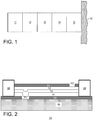
- FIG. 1 illustrates a typical five layer solid-state electrochromic device in cross-section having the five following superimposed layers: an electrochromic electrode layer (“EC") 14 which produces a change in absorption or reflection upon oxidation or reduction; an ion conductor layer (“IC”) 13 which functionally replaces an electrolyte, allowing the passage of ions while blocking electronic current; a counter electrode layer (“CE”) 12 which serves as a storage layer for ions when the device is in the bleached or clear state; and two transparent conductive layers (“TCLs”) 11 and 15 which serve to apply an electrical potential to the electrochromic device.
- EC electrochromic electrode layer
- IC ion conductor layer
- CE counter electrode layer
- TCLs transparent conductive layers
- FIG. 2 illustrates the electrochromic device of FIG. 1 , in cross-section, having power supplied from two conductive elements, such as busbars 18 and 19.
- the busbars are electrically isolated from one another. Conventionally, this is done by scribing the TCLs 11 and 15. As shown in FIG. 2 , the first (lower) TCL 15 is scribed at point P1, making the lower TCL 15 a discontinuous (i.e., physically separate) layer, and thereby preventing the busbars from shorting across the lower TCL 15.
- the width of the scribe at point P1 is typically on the order of 25 microns or wider, while the length varies based on the width the particular device being formed.
- the second (upper) TCL 11 is scribed at point P3, making the upper TCL 11 also discontinuous, and thereby preventing the busbars from being shorted together across the upper TCL 11.
- the P3 scribe is typically on the order to 25 microns or wider, while the length varies based on the width the particular device being formed.
- An intrinsic property of the EC layer 14 is that it becomes conductive when it transitions to a colored state.
- inserting electrons and charge compensating ions (such as lithium ions) into the EC material 14 leads to the material transitioning from an insulating state to a conductive state. This transition can happen upon the inserted (or "intercolated") electrons or charge compensating ions reaching a threshold concentration, whereupon the EC device transitions suddenly to a conductive state.
- insertion of the charge compensating ions will not occur above the P1 scribe itself, as no electric field is generated there due to the absence of the lower transparent conductive layer.
- charge compensating ions can migrate laterally (i.e ., sideways in FIG. 2 ) in the layer according to the usual laws of diffusion.
- a threshold concentration of charge compensating ions migrate laterally into a material, the material becomes conductive.
- the distance that the threshold concentration of charge compensating ions are capable of diffusing laterally will hereinafter be termed the "migration length.”
- a conductive region can form in the area of the P1 scribe.
- the two portions 15a and 15b of the lower TCL 15 may be conductively connected by the conductive region. For example, as shown in FIG.
- the portion of the EC layer 14 may be colored for a reasonable amount of time. During this time, lithium can diffuse laterally across the P1 scribe, converting the EC layer 14 in that area 17 from an insulating layer to a conducting layer. If the scribed channel between the two portions 15a and 15b of the lower TCL 15 is not wide enough, current may pass between these portions, thereby electrically shorting the busbars 18 and 19 together.
- the area 17 cannot simply be converted back from a conducting region to an insulating region, since clearing the electrochromic device 10 will not apply an electric field to that region of the device 10 in order for it to bleach ( i.e ., transition from a colored state to a non-colored state or a less colored state).
- the yield can be considered to be reduced every time a substrate or other workpiece is cycled between vacuum and atmosphere and vice versa. It is believed. that this may be caused by dust and debris from the coating process, which is inevitably present in sputtering and which may be 'blown' around during venting and pumpdown, finding its way onto the active layers, leading to potential defects in the film structure, such as short circuits or "shorts.”
- depositing all of the layers in one single continuous vacuum step i.e., one coating machine, would achieve a high yield.
- US 5,724,175 A discloses methods for manufacturing electrochromic devices using laser patterning techniques.
- WO 2013/090209 A1 discloses thin-film devices, for example electrochromic devices for windows, and methods of manufacturing.
- US 2011/0211247 A1 discloses electrochromic devices with low defectivity fabricated by depositing certain layered components of the electrochromic device in a single integrated deposition system.
- an electrochromic device including a lower transparent conductive layer.
- a first portion of the lower transparent conductive layer may be coupled to a first conductive element.
- a second portion, physically separate from the first portion, of the lower transparent conductive layer may be coupled to a second conductive element.
- the electrochromic device may also include an upper transparent conductive layer.
- a first portion of the upper transparent conductive layer may be coupled to the first conductive element.
- a second portion, physically separate from the first portion, of the upper transparent conductive layer may be coupled to the second conductive element.
- the electrochromic device may also include a first electrode layer comprising one of a counter electrode layer and an electrochromic layer.
- the first electrode layer may be between the lower transparent conductive layer and the upper transparent conductive layer, and may be in contact with each of the first portion and the second portion of the lower conductive layer.
- the electrochromic device may also include a second electrode layer comprising the other of the counter electrode layer and the electrochromic electrode layer.
- the second electrode layer may also be between the lower transparent conductive layer and the upper transparent conductive layer.
- the electrochromic device may further include an ion-conductor layer for conducting ions between and in communication with the first electrode layer and the second electrode layer.
- the ion-conductor extends continuously from the first conductive element to the second conductive element.
- the first portion and second portion of the lower transparent conductive layer are spaced apart more than the migration length, which is defined in greater detail herein.
- the first portion and second portion of the lower transparent conductive layer are spaced more than about 25 microns apart. In some embodiments, they may be spaced more than about 50 microns apart. In some embodiments, they may be spaced more than about 75 microns apart.
- the space between the first portion and second portion of the lower transparent conductive layer may be filled at least partially by the first electrode layer.
- the space between the first portion and second portion of the lower transparent conductive layer is filled at least partially by a third portion of the lower transparent conductive layer that is electrically isolated from each of the first portion and the second portion of the lower transparent conductive layer.
- the first portion and third portion of the lower transparent conductive layer may then spaced more than about 25 microns apart, and the second portion and third portion of the lower transparent conductive layer may also be spaced more than about 25 microns apart.
- the first portion and second portion of the lower transparent conductive layer may be spaced more than about 50 microns apart.
- the first portion and second portion of the lower transparent conductive layer may be spaced more than about 75 microns apart.
- the respective spaces between the first portion and third portion, and between the second portion and the third portion, of the lower transparent conductive layer may each be filled at least partially by the first electrode layer.
- the first conductive electrode layer may comprise a first portion coupled to the first conductive element and to the first portion of the lower transparent conductive layer, and a second portion, physically separate from the first portion, coupled to the second conductive element and to the second portion of the transparent conductive layer.
- the first portion and second portion of the lower transparent conductive layer may be spaced apart more than the first portion and second portion of the first electrode layer are spaced apart.
- the space between the first portion and second portion of the lower transparent conductive layer may be filled at least partially by the ion conductor layer.
- the space between the first portion and second portion of the first electrode layer is filled at least partially by the ion conductor layer.
- the counter electrode layer may comprise a mixed tungsten nickel oxide. In some further embodiments, the counter electrode layer may comprise lithium ions.
- Another aspect of the invention provides a method for the preparation of an electrochromic device according to claim 12.
- the method includes inter alia providing a first conductive layer, cutting the first conductive layer such that a first portion of the first conductive layer is electrically isolated from a second portion of the first conductive layer, depositing one of an electrochromic electrode layer and a counter electrode layer on said first conductive layer, thereby providing a first deposited electrode that is occupied by a charge compensating ion having a diffusion length that is shorter than the space between the first portion and second portion of the first conductive layer, depositing an ion-conductor layer on the first deposited electrode, such that said ion transparent layer is in communication with the first deposited electrode, depositing the other of the electrochromic electrode layer and said counter electrode layer on the ion-conductor layer, thereby providing a second deposited electrode, and depositing a second conductive layer on the second deposited electrode.
- the first deposited electrode may be deposited over the first and second portions of the first conductive layer, and the first and second portions may be spaced more than about 25 microns apart. In some embodiments, they may be spaced more than about 50 microns apart. In some embodiments, they may be spaced more than about 75 microns apart.
- the first deposited electrode may be deposited over the first and second portions of the first conductive layer such that the space between the first portion and second portion of the first conductive layer is filled at least partially by the first deposited electrode.
- the method further includes cutting the second portion of the first conductive layer such the first conductive layer is divided into three electrically isolated portions, one of the portions being a middle portion positioned between the other two outer portions.
- the space between the middle portion and each of the outer portions may be filled at least partially by the first electrode Layer.
- the first cutting step may be performed before the first electrode layer is deposited on the first conductive layer.
- the second cutting step may be performed after the first electrode layer is deposited on the first conductive layer such that first electrode layer comprises a first portion coupled to the first portion of the first conductive layer, and a second portion, physically separate from the first portion, coupled to the second portion of the first conductive layer, and such that the first portion and second portion of the first conductive layer are spaced apart more than the first portion and second portion of the first electrode layer are spaced apart.
- the space between the first portion and second portion of the first conductive layer may be filled at least partially by the ion conductor layer. In some embodiments, the space between the first portion and second portion of the first electrode layer may be filled at least partially by the ion conductor layer.
- One object of the present invention is to provide an electrochromic device having improved insulating film structure to reduce electronic leakage (e.g., between electrically isolated portions of a transparent conductor layer).
- the disclosed electrochromic devices are formed using a deposition process having either two or three coating processes with either one or two laser processing steps, respectively, between them (not including laser scribing processing steps that may be performed subsequent to the deposition process).
- the disclosed devices and processes therefore involve minimal vacuum cycling, thereby potentially increasing yield.
- Yet another objective of the present invention is to provide a method of preparing an electrochromic device comprising the improved insulating film structure.
- Yet another objective of the present invention is to provide a method of preparing an improved insulating film structure for use in electrochromic devices.
- FIG. 4 illustrates a portion of a solid-state electrochromic device 40, in cross-section, having an improved insulating film structure.
- the device 40 of FIG. 4 when complete, is similar to the solid-state device depicted in FIGS. 1 and 2 to the extent that each of the aforementioned EC, IC, CE, and upper TCL layers, 11-14 are also present in the device of FIG. 4 .
- the device of FIG. 4 when complete, differs from the device depicted in FIGS. 1 and 2 to the extent that the P1 scribe at location P1 is wider than the P1 scribe of FIGS. 1 and 2 .
- the Linewidth of the P1 scribe is greater than about 25 microns.
- the linewidth may be greater than about 50 microns, and in further examples, the linewidth may be greater than about 75 microns.
- the left and right portions of the lower transparent conductor layer, 45a and 45b respectively, are thus separated by a wide P1 scribe positioned at location P1 of the device.
- the resistance across location P1 would be infinite so as to electrically isolate the two portions 45a and 45b of the lower transparent conductor layer 45.
- increasing the linewidth of the scribe in turn increases the resistance at location P1 between the lower TCL portions 45a and 45b.
- the EC layer 44 of the device of FIG. 4 fills in the gap, either completely or partially, formed by the P1 scribe.
- the channel separating the lower TCL portions 45a and 45b is filled with materials that are not electrically conductive.
- the linewidth of the channel is chosen such that it is greater than the migration length of the lithium ions in the EC layer 44.
- the linewidth of the channel is chosen to be wider than the distance that the charge compensating ions in the EC layer 44 are capable of diffusing sideways. This ensures that a conductive path extending from one portion of the TCL 45a to the other portion 45b is not formed in the EC layer 44 when the electrochromic device 40 is held in a colored state for a significant amount of time.
- FIG. 5 illustrates a cross-section of a portion of yet another solid-state electrochromic device 50 also, when completed, having an insulating film structure also improved upon the structure of the device of FIGS. 1 and 2 .
- the device 50 of FIG. 5 is similar to the solid-state device 40 depicted in FIG. 4 to the extent that each of the aforementioned layers (i.e., layers 11-14 of FIG. 2 ) are formed on top of the lower TCL 55 of the portion of the device 50 shown in FIG. 5 .
- the device 50 of FIG. 5 differs from that of FIG. 4 to the extent that the device 50 of FIG.
- the lower TCL 55 includes a doublet, two isolated scribes in the lower TCL 55.
- the lower TCL 55 is divided into three sections: left section 55a which is electrically connected to a first busbar 58, right section 55c which is electrically connected to a second busbar 59, and middle section 55b which is electrically isolated from the left section 55a by a first scribe P1a, and is electrically isolated from the right section 55c by a second scribe P1b.
- the formation of the doublet depicted in FIG. 5 has the same effect as making a fully depleted line across the P1 location (i.e., fully cutting the middle section 55b out of the device 50).
- the EC layer 54 fills in the gaps, either completely or partially, formed by the P1a and P1b cuts.
- the channel separating the lower TCL left and middle sections 55a and 55b, as well as the channel separating the middle and right sections 55b and 55c, are each filled with materials that are not electrically conductive.
- the effective linewidth of the doublet is chosen such that it is greater than the migration length of the lithium ions occupying the EC layer 54. This ensures that a conductive path extending from the left section of the TCL 55a to the right section 55c is not formed in the EC layer 54 when the electrochromic device 50 is held in a colored state for a significant amount of time.
- each of the gaps may be very narrow ( e.g. , 10 microns wide, 5 microns wide, or even less) provided that each gap completely severs the lower TCL and that the distance between the left section 55a and right section 55c of the lower TCL is greater than the migration length of the conducting ions in the EC layer.
- the TCL portions may further be electrically isolated from one another by cutting the EC layer at location P1.
- FIG. 6 illustrates a cross-section of a portion of yet another solid-state electrochromic device 60 also, when completed, having an insulating film structure improved upon the structure of the device of FIGS. 1 and 2 .
- the device 60 of FIG. 6 is similar to the solid-state device 40 depicted in FIG. 4 to the extent that each of the aforementioned upper TCL, CE, and IC layers (i.e., layers 11-13 of FIG. 2 ) are formed on top of the lower TCL 65 of the portion of the device 60 shown in FIG. 6 .
- the device 60 of FIG. 6 differs from that of FIG.
- the EC layer 64 of device 60 is cut into portions 64a and 64b, each portion electrically isolated from the other, at location P1.
- the left portion 64a of the EC layer is electrically connected to the first busbar 68 and to the left portion of the lower TCL 65a.
- the right portion 64b of the EC layer is electrically connected to the second busbar 69 and the right portion of the upper TCL 65b.
- the cut separating the portions of the EC layer 64 is narrower (has a smaller linewidth) than the cut separating the portions of the lower TCL 65 underneath. Due to the additional cut through the EC layer 64, the channel between the left and right portions of the lower TCL 65 is filled only partially with the EC layer 64. The remainder of the channel is filled with the insulating IC layer 63.
- the cut separating the portions of the EC layer 64 may be narrower than the migration length of the conductive ions in the EC layer.
- the cut may be about 10 microns, about 5 microns, or even narrower. Effectively, there is no minimum for the width of this cut, so long as it fully severs the layer deposited underneath. This is because the second results in the formation of an EC layer / IC layer (or EC layer / CE layer) interface that functions essentially like a "blocking" contact between the separated portions of the lower TCL. This interface is believed to behave more like a diode than a resistance and is therefore much more effective at blocking migration of the conducting ions, even along a distance shorter than the migration length.
- composition or type of layers which are deposited may be varied in order to achieve the desired results without departing from the teachings of the present invention.
- FIG. 7 provides a flow diagram 700 that illustrates a process by which the device 40, a portion of which is shown in FIG. 4 , and device 50, a portion of which is shown in FIG. 5 , may be formed in their entirety.
- a lower transport conductive layer is deposited onto a substrate such that the lower transport conductive layer extends continuously from the first busbar to the second busbar.
- the materials comprising a conductor layer are deposited via sputtering onto a transparent substrate to form a first transparent conductor layer.
- the lower transport conductive layer is scribed or cut at location P1.
- the scribe may be accomplished using one of several different methods, including laser scribing, etching, mechanical abrading or other suitable removing processes known in the art ("cutting").
- the cutting may be performed in a variety of different ways and/or methods, such as by use of a suitable masking, scribing or etching processes that utilize one or more of a laser, a mechanical abrasion process involving, for example, use of a diamond, ruby or stainless steel tip, electrical discharge machining, or chemical etching.
- the linewidth of the cut may be significantly increased by performing multiple cuts one next to another.
- the linewidth may be effectively increased by performing two or more cuts spaced apart from each other such that the material remaining from the TCL between the two or more cuts is electrically isolated from both the first and second busbars of the device.
- an electrochromic (EC) electrode layer (also called the "first electrode” herein), is then deposited on the lower TCL such that the EC layer extends continuously from the first busbar to the second busbar.
- the first electrode is deposited via intermediate frequency reactive sputtering or DC sputtering techniques. In some embodiments, the first electrode layer is deposited on a heated lower transparent conductor layer.
- an ion conductor layer is then deposited on the electrochromic electrode layer such that the ion conductor layer extends continuously from the first busbar to the second busbar.
- the ion conductor layer may be comprised of a solid electrolyte capable of allowing ions to migrate through the layer.
- the ion conductor layer must have a sufficient ionic transport property to allow ions, preferably lithium ions, to migrate through. Any material may be used for an ion conductor provided it allows for the passage of ions from the CE layer to the EC layer.
- the ion conductor layer comprises a silicate-based structure.
- suitable ion conductors particularly adapted for lithium ion transmission include, but are not limited to, lithium silicate, lithium aluminum silicate, lithium aluminum borate, lithium borate, lithium zirconium silicate, lithium niobate, lithium borosilicate, lithium phosphosilicate, lithium nitride, lithium aluminum fluoride, and other such lithium-based ceramic materials, silicas, or silicon oxides.
- Other suitable ion-conducting materials can be used, such as silicon dioxide or tantalum oxide.
- the ion conductive layer has low or no electronic conductivity.
- the preferred ion conductor material is a lithium-silicon-oxide produced by either sputtering or a sol-gel process.
- the ion conductor layer is deposited by intermediate frequency reactive sputtering or DC sputtering techniques. In other preferred embodiments, the ion conductor layer is deposited by sol-gel thin film deposition techniques including dip coating, spin coating and spray coating. In yet other preferred embodiments, the ion conductor layer is deposited by sputtering or by sol-gel techniques. The procedures for depositing such layers by sputtering or sol-gel coating are known to those skilled in the art.
- a counter electrode (CE) layer (also called a "second electrode” layer herein), is then deposited on the ion conductor layer such that the CE layer extends continuously from the first busbar to the second busbar.
- the CE layer may be an anodic complementary CE layer, such as mixed tungsten-nickel oxides, and preferably substantially crystalline mixed tungsten-nickel oxides, as described in U.S. Patent No. 7,372,610 , the disclosure of which is hereby incorporated by reference in its entirety herein.
- Complementary CE layers may comprise a charge compensating ion, such as lithium.
- the charge compensating ion may be at least partially intercalated within the mixed tungsten-nickel oxide, and/or present as a film at least partially coating the surface of the CE layer.
- the charge compensating ion is capable of being reversibly transferred from the CE layer to the EC layer when an appropriate electrical potential is applied.
- the deposited film is reduced through the deposition of lithium.
- the deposition of the lithium is achieved through one of either wet chemical methods, sol-gel, chemical vapor deposition, physical vapor deposition, or non-reactive sputtering.
- the source of the lithium deposited on the tungsten-nickel oxide film is lithium metal deposited in vacuum using a non-reactive sputtering process.
- the amount of lithium deposited on the anodic mixed tungsten-nickel oxide film is carefully controlled such that an amount of lithium is added that allows for the greatest transmission of light through the CE layer, and hence the whole device.
- charge compensating ions such as protons (H), lithium ions (Li + ), or sodium ions (Na + ), are intercalated into the electrochromic device.
- the term "intercalation” means the reversible insertion of a molecule, atom or ion into the lattice of an electrochromic device layer.
- the charge compensating ion is lithium.
- the lithium ions are deposited by magnetron sputter deposition of atomic lithium from a metallic sputter target into the device, under vacuum processing conditions.
- a lithium oxide or lithium carbonate may be deposited in place of metallic lithium using any known means of deposition (e.g., sputtering, etc.).
- the intercalation step occurs after the deposition of one or both of the electrode layers.
- the amount of charge compensating ion deposited is carefully controlled such that an amount of charge compensating ion is added that maximizes the dynamic range, of the electrochromic device.
- an upper transparent conductive layer is deposited on the counter electrode layer by methods well known in the art and as described above in the deposition of the first transparent conductive layer.
- all of the layers comprising the electrochromic device are deposited via magnetron sputter deposition in the same vacuum processing chamber so as to increase device fabrication manufacturability, meaning that the yields are likely to be improved as a result of reduced handling, and the throughput is also likely to be increased as a result of fewer processing steps. Moreover, depositing all of the layers in the same chamber would result in a reduction in the number of shorts.
- the transparent conductor, EC, IC, and CE layers may be deposited by any technique known in the art including wet chemical methods, chemical vapor deposition, or physical vapor deposition.
- Preferred methods of deposition include sol-gel, spray pyrolysis, electrodeposition, metallo-organic decomposition, laser ablation, pulsed laser ablation, evaporation, e-beam assisted evaporation, sputtering, intermediate frequency reactive sputtering, RF sputtering, magnetron sputtering, DC sputtering, reactive DC magnetron sputtering and the like.
- the heat treatment process is believed to have a positive effect on the switching characteristics of the electrochromic device, as well as improving the conductivity and transparency of the second electrode layer (i.e., the electrode layer adjacent to the upper TCL).
- the heat treatment also is believed to have the effect of increasing the transmission of the lithiated CE layer.
- Flow diagram 800 illustrates a process by which the device 60, a portion of which is shown in FIG. 6 , may be formed in its entirety.
- the steps described in blocks 802-806, and 810-816 are respectively comparable to steps 702-714 described in connection with flow diagram 700 and are therefore not repeated here.
- Flow diagram 800 includes an additional step, block 808.
- the EC layer is scribed or cut at location P1, above the scribe in the lower transparent conductor layer underneath the EC layer.
- the EC layer scribe may have a narrower linewidth than the lower TC layer scribe, such that only a portion of the EC layer materials deposited at and occupying the channel between the lower TC layer portions at location P1 are scribed, while some of the EC layer materials remain deposited in the channel.
- the channel formed through the P1 cut is filled by the EC layer.
- the linewidth of the channel is chosen to exceed the migration length of the lithium ions (which, as described above, are intercalated into the device).
- the channel formed in the TCL is filled partly by the EC layer and partly by the IC layer above the EC layer.
- the IC layer does not become conductive when the device is held in a colored state.
- the channel formed at location P1 therefore cannot become completely conductive.
- the channel between the left and right portions 65a and 65b of the TCL (i.e., the linewidth of the first P1 scribe formed at block 804) of FIG. 6 need not necessarily be as wide as that of the channel formed between the left and right portions of the TCLs of either FIG. 4 or FIG. 5 in order to prevent shorting of the lower TCL.
- Each of the layers included in the devices 40, 50, and 60 may be formed using the materials and techniques described in U.S. Patent No. 8,004,744 , and concurrently pending application 13/786,934 , which is entitled "Laser Cuts to Reduce Electrical Leakage,” the disclosures of which are hereby incorporated by reference herein in their entirety.
- the layers of the devices may be formed sequentially, beginning with the bottom TCL and working upward to the upper TCL.
- one or more optical tuning layers may be deposited above the upper TCL, as described more fully in U.S. Patent No. 5,724,177 , the disclosure of which is hereby incorporated by reference in its entirety herein.
- optical tuning layers may be used in combination with conductive metal layers and preferably have a thickness between about 10 nm and about 50 nm, and more preferably between about 23 nm and about 40 nm.
- Preferred materials for forming optical tuning layers have an index of refraction which is greater than about 1.9, and more preferably between about 1.9 and about 2.8.
- the index of refraction and thickness of an optical tuning layer may be selected using the following method.
- the desired index of refraction may be determined by multiplying the index of refraction of the glass substrate by the index of refraction of the transparent conductive layer and taking the square root of the product.
- the thickness of optical tuning layer 61 is then determined by dividing the visible light wavelength (e.g., 540 nm) by the calculated index of refraction.
- the thickness of optical tuning layer is about 75 nm.
- the glass substrate has an index of refraction of 1.5
- the first optical tuning layer has an index of refraction of about 1.77 and a thickness of about 75 nm
- the lower transparent conductive oxide layer has an index of refraction of about 2.1 and a thickness of about 450 nm
- the electrochromic electrode layer has an index of refraction of about 2.1 and a thickness of about 400 nm
- the ion conducting layer has an index of refraction of about 1.5 and a thickness of about 200 nm
- the counter electrode layer has an index of refraction of about 2.0 and a thickness of about 200 nm
- the upper transparent conductive layer has an index of refraction of about 2.1 and a thickness of about 450 nm
- the second optical tuning layer has an index of refraction of about 1.77 and a thickness of about 75 nm.
- a glass superstrate and a laminate layer for adhering a glass superstrate to the optical tuning layer, each having an index of refraction of about 1.5
- the glass substrate has an index of refraction of about 1.5
- the first optical tuning layer has an index of refraction of about 2.1 and a thickness of about 20 nm
- the second adjacent optical tuning layer has an index of refraction of about 1.5 and a thickness of about 29 nm
- the lower transparent conductive layer has an index of refraction of about 2.1 and a thickness of about 450 nm
- the electrochromic electrode layer has an index of refraction of about 2.1 and a thickness of about 300 nm
- the ion conducting layer has an index of refraction of about 2.0 and a thickness of about 200 nm
- the counter electrode layer has an index of refraction of about 2.0 and a thickness of about 200 nm
- the upper transparent conductive layer has an index of refraction of about 2.1 and a thickness of about 450 nm
- the laminate layer has an index of refraction of about 1.5
- the glass superstrate has an index of refraction of about 1.5.
- the lower transparent conductive layer may be optically tuned by the use of two or more optical tuning layers selected so that the indices of refraction of the various layers gradually increase from the index of refraction of substrate to the index of refraction of the lower transparent conductive layer.
- the optical tuning layers may be two or more layers of monotonically increasing index of refraction.
- the first optical tuning layer will desirably have an index of refraction of about 1.62 ((1.5 2 ⁇ 1.9) 1/3 ), and the second optical tuning layer will desirably have an index of refraction of about 1.76 ((1.5 ⁇ 1.9 2 ) 1/3 ).
- the thicknesses of layers are desirably about 60 nm and 53 nm, respectively, as determined by optical modeling to achieve maximum transmission. Where desirable, a series of more than two adjacent optical tuning layers may be used to further enhance the optical tuning affect.
- the EC layer is deposited below the IC layer (s) (e.g ., closer to the substrate, closer to the lower TCL), and the CE layer is deposited above the IC layer(s) (e.g., closer to the upper TCL).
- the placement of the EC and CE layers may be switched, such that the CE layer is positioned below the IC layer(s) and the EC layer is positioned above the IC layers(s).
- the P1 scribe may cut through the CE layer instead of through the EC layer, and the P3 scribe may cut through the TCL closer to the EC layer.
- the electrochromic stack may be formed in the reverse order on the substrate.
- the bottom two or three formed layers depending on the embodiment (i.e., the transparent conductor layer adjacent to the substrate, the CE layer, and in some embodiments the IC layer adjacent to the CE layer), may be cut at location P1.
- each of the above embodiments illustrates an electrochromic structure between only two busbars
- each of the busbars may be electrically separated from each other by forming the electrochromic structures as described above. Forming of each of the electrochromic structures may be performed simultaneously or sequentially, and the layers formed between each pair of busbars may be scribed in any of the manners described above.
- the embodiments described above and illustrated in the figures are not limited to rectangular shaped electrochromic devices. Rather, the descriptions and figures are meant only to depict cross-sectional views of an electrochromic device and are not meant to limit the shape of such a device in any manner.
- the electrochromic device may be formed in shapes other than rectangles (e.g., circles, etc.).
- the electrochromic device may be shaped three-dimensionally ( e.g., convex, concave, etc.).
Description
- The present invention relates to electrochromic devices and more particularly relates to solid-state, inorganic thin film devices.
- Electrochromic materials and devices have been developed as an alternative to passive coating materials for light and heat management in building and vehicle windows. In contrast to passive coating materials, electrochromic devices employ materials capable of reversibly altering their optical properties following electrochemical oxidation and reduction in response to an applied potential. The optical modulation is the result of the simultaneous insertion and extraction of electrons and charge compensating ions in the electrochemical material lattice.
- In general, electrochromic devices ("EC devices") have a composite structure through which the transmittance of light can be modulated.
FIG. 1 illustrates a typical five layer solid-state electrochromic device in cross-section having the five following superimposed layers: an electrochromic electrode layer ("EC") 14 which produces a change in absorption or reflection upon oxidation or reduction; an ion conductor layer ("IC") 13 which functionally replaces an electrolyte, allowing the passage of ions while blocking electronic current; a counter electrode layer ("CE") 12 which serves as a storage layer for ions when the device is in the bleached or clear state; and two transparent conductive layers ("TCLs") 11 and 15 which serve to apply an electrical potential to the electrochromic device. Each of the aforementioned layers is typically applied sequentially on asubstrate 16. Such devices typically suffer from intrinsic electronic leakage (between the electrochromic stack layers) and electronic breakdown. - Typically, electrical power is distributed to the electrochromic device through busbars.
FIG. 2 illustrates the electrochromic device ofFIG. 1 , in cross-section, having power supplied from two conductive elements, such asbusbars FIG. 2 , the first (lower)TCL 15 is scribed at point P1, making the lower TCL 15 a discontinuous (i.e., physically separate) layer, and thereby preventing the busbars from shorting across thelower TCL 15. The width of the scribe at point P1 is typically on the order of 25 microns or wider, while the length varies based on the width the particular device being formed. Similarly, the second (upper)TCL 11 is scribed at point P3, making theupper TCL 11 also discontinuous, and thereby preventing the busbars from being shorted together across theupper TCL 11. Similar to the dimensions of the P1 scribe, the P3 scribe is typically on the order to 25 microns or wider, while the length varies based on the width the particular device being formed. - An intrinsic property of the
EC layer 14 is that it becomes conductive when it transitions to a colored state. In other words, inserting electrons and charge compensating ions (such as lithium ions) into theEC material 14 leads to the material transitioning from an insulating state to a conductive state. This transition can happen upon the inserted (or "intercolated") electrons or charge compensating ions reaching a threshold concentration, whereupon the EC device transitions suddenly to a conductive state. Under ideal operation of the EC device, insertion of the charge compensating ions will not occur above the P1 scribe itself, as no electric field is generated there due to the absence of the lower transparent conductive layer. However, it is possible that charge compensating ions can migrate laterally (i.e., sideways inFIG. 2 ) in the layer according to the usual laws of diffusion. Moreover, when a threshold concentration of charge compensating ions migrate laterally into a material, the material becomes conductive. The distance that the threshold concentration of charge compensating ions are capable of diffusing laterally will hereinafter be termed the "migration length." Should the migration length meet or exceed the P1 scribe width, a conductive region can form in the area of the P1 scribe. Furthermore, if the conductive region extends across the full width of the P1 scribe, the two portions 15a and 15b of thelower TCL 15 may be conductively connected by the conductive region. For example, as shown inFIG. 3 , the portion of theEC layer 14 may be colored for a reasonable amount of time. During this time, lithium can diffuse laterally across the P1 scribe, converting theEC layer 14 in thatarea 17 from an insulating layer to a conducting layer. If the scribed channel between the two portions 15a and 15b of thelower TCL 15 is not wide enough, current may pass between these portions, thereby electrically shorting thebusbars area 17 cannot simply be converted back from a conducting region to an insulating region, since clearing theelectrochromic device 10 will not apply an electric field to that region of thedevice 10 in order for it to bleach (i.e., transition from a colored state to a non-colored state or a less colored state). - Furthermore, in order to produce electrochromic devices in a more cost effective manner, it is necessary to modify the deposition process to provide for higher yields and to be more amenable to mass production. In general, the yield can be considered to be reduced every time a substrate or other workpiece is cycled between vacuum and atmosphere and vice versa. It is believed. that this may be caused by dust and debris from the coating process, which is inevitably present in sputtering and which may be 'blown' around during venting and pumpdown, finding its way onto the active layers, leading to potential defects in the film structure, such as short circuits or "shorts." Thus, depositing all of the layers in one single continuous vacuum step, i.e., one coating machine, would achieve a high yield. However, to produce the structure shown in
FIG 3 , depositing all the layers in a single vacuum step would require including a Laser scribe (or cut of some type) between the deposition of the lower transparent conductor and the deposition of the second transparent conductor in the same vacuum system. Such cutting processes are very difficult in a vacuum system. For instance, with regard to laser scribing, it is necessary to maintain an extremely tight focus for the laser. Such focus is very difficult to achieve efficiently with the mechanical tolerances present in typical commercial sputtering systems. - It is desirable to reduce the amount of electronic leakage between the portions of the transparent conducting layers of the electrochromic device while maintaining as high a yield as possible (e.g., conducting as few scribing steps during the cutting process as possible).
-
US 5,724,175 A discloses methods for manufacturing electrochromic devices using laser patterning techniques. -
WO 2013/090209 A1 discloses thin-film devices, for example electrochromic devices for windows, and methods of manufacturing. -
US 2011/0211247 A1 discloses electrochromic devices with low defectivity fabricated by depositing certain layered components of the electrochromic device in a single integrated deposition system. - Subject matter of the present invention is an electrochromic device as defined in claim 1, and a method for the preparation of an electrochromic device as defined in
claim 12. The dependent claims relate to particular embodiments thereof. - One aspect of the disclosure provides an electrochromic device including a lower transparent conductive layer. A first portion of the lower transparent conductive layer may be coupled to a first conductive element. A second portion, physically separate from the first portion, of the lower transparent conductive layer may be coupled to a second conductive element. The electrochromic device may also include an upper transparent conductive layer. A first portion of the upper transparent conductive layer may be coupled to the first conductive element. A second portion, physically separate from the first portion, of the upper transparent conductive layer may be coupled to the second conductive element.
- The electrochromic device may also include a first electrode layer comprising one of a counter electrode layer and an electrochromic layer. The first electrode layer may be between the lower transparent conductive layer and the upper transparent conductive layer, and may be in contact with each of the first portion and the second portion of the lower conductive layer. The electrochromic device may also include a second electrode layer comprising the other of the counter electrode layer and the electrochromic electrode layer. The second electrode layer may also be between the lower transparent conductive layer and the upper transparent conductive layer.
- The electrochromic device may further include an ion-conductor layer for conducting ions between and in communication with the first electrode layer and the second electrode layer. The ion-conductor extends continuously from the first conductive element to the second conductive element.
- The first portion and second portion of the lower transparent conductive layer are spaced apart more than the migration length, which is defined in greater detail herein. In other words, the first portion and second portion of the lower transparent conductive layer are spaced more than about 25 microns apart. In some embodiments, they may be spaced more than about 50 microns apart. In some embodiments, they may be spaced more than about 75 microns apart.
- In some embodiments, the space between the first portion and second portion of the lower transparent conductive layer may be filled at least partially by the first electrode layer. According to the present disclosure, the space between the first portion and second portion of the lower transparent conductive layer is filled at least partially by a third portion of the lower transparent conductive layer that is electrically isolated from each of the first portion and the second portion of the lower transparent conductive layer. The first portion and third portion of the lower transparent conductive layer may then spaced more than about 25 microns apart, and the second portion and third portion of the lower transparent conductive layer may also be spaced more than about 25 microns apart. Thus, the first portion and second portion of the lower transparent conductive layer may be spaced more than about 50 microns apart. In some embodiments, the first portion and second portion of the lower transparent conductive layer may be spaced more than about 75 microns apart. The respective spaces between the first portion and third portion, and between the second portion and the third portion, of the lower transparent conductive layer may each be filled at least partially by the first electrode layer.
- In some embodiments, the first conductive electrode layer may comprise a first portion coupled to the first conductive element and to the first portion of the lower transparent conductive layer, and a second portion, physically separate from the first portion, coupled to the second conductive element and to the second portion of the transparent conductive layer. The first portion and second portion of the lower transparent conductive layer may be spaced apart more than the first portion and second portion of the first electrode layer are spaced apart. The space between the first portion and second portion of the lower transparent conductive layer may be filled at least partially by the ion conductor layer. The space between the first portion and second portion of the first electrode layer is filled at least partially by the ion conductor layer.
- In some of the above embodiments, the counter electrode layer may comprise a mixed tungsten nickel oxide. In some further embodiments, the counter electrode layer may comprise lithium ions.
- Another aspect of the invention provides a method for the preparation of an electrochromic device according to
claim 12. The method includes inter alia providing a first conductive layer, cutting the first conductive layer such that a first portion of the first conductive layer is electrically isolated from a second portion of the first conductive layer, depositing one of an electrochromic electrode layer and a counter electrode layer on said first conductive layer, thereby providing a first deposited electrode that is occupied by a charge compensating ion having a diffusion length that is shorter than the space between the first portion and second portion of the first conductive layer, depositing an ion-conductor layer on the first deposited electrode, such that said ion transparent layer is in communication with the first deposited electrode, depositing the other of the electrochromic electrode layer and said counter electrode layer on the ion-conductor layer, thereby providing a second deposited electrode, and depositing a second conductive layer on the second deposited electrode. - The first deposited electrode may be deposited over the first and second portions of the first conductive layer, and the first and second portions may be spaced more than about 25 microns apart. In some embodiments, they may be spaced more than about 50 microns apart. In some embodiments, they may be spaced more than about 75 microns apart.
- The first deposited electrode may be deposited over the first and second portions of the first conductive layer such that the space between the first portion and second portion of the first conductive layer is filled at least partially by the first deposited electrode.
- According to the present disclosure, the method further includes cutting the second portion of the first conductive layer such the first conductive layer is divided into three electrically isolated portions, one of the portions being a middle portion positioned between the other two outer portions. The space between the middle portion and each of the outer portions may be filled at least partially by the first electrode Layer.
- The first cutting step may be performed before the first electrode layer is deposited on the first conductive layer. The second cutting step may be performed after the first electrode layer is deposited on the first conductive layer such that first electrode layer comprises a first portion coupled to the first portion of the first conductive layer, and a second portion, physically separate from the first portion, coupled to the second portion of the first conductive layer, and such that the first portion and second portion of the first conductive layer are spaced apart more than the first portion and second portion of the first electrode layer are spaced apart. The space between the first portion and second portion of the first conductive layer may be filled at least partially by the ion conductor layer. In some embodiments, the space between the first portion and second portion of the first electrode layer may be filled at least partially by the ion conductor layer.
-
-
FIG. 1 is a schematic cross-section of a typical electrochromic device. -
FIG. 2 is another schematic cross-section of a typical electrochromic device. -
FIG. 3 is the schematic cross-section ofFIG. 2 showing a close-up of a portion of the electrochromic device. -
FIG. 4 is a schematic cross-section of part of an electrochromic device having an improved structure. -
FIG. 5 is a schematic cross-section of part of an electrochromic device having an improved structure in accordance with the current invention. -
FIG. 6 is a schematic cross-section of part of another electrochromic device having an improved structure. -
FIG. 7 is a flow chart depicting a process for forming an electrochromic device. -
FIG. 8 is a flow chart depicting a process for forming an electrochromic device. - One object of the present invention is to provide an electrochromic device having improved insulating film structure to reduce electronic leakage (e.g., between electrically isolated portions of a transparent conductor layer). The disclosed electrochromic devices are formed using a deposition process having either two or three coating processes with either one or two laser processing steps, respectively, between them (not including laser scribing processing steps that may be performed subsequent to the deposition process). The disclosed devices and processes therefore involve minimal vacuum cycling, thereby potentially increasing yield. These and other objectives are realized by means of an electrochromic device utilizing a transparent conductor layer having a wider, or effectively wider, channel width at location P1.
- Yet another objective of the present invention is to provide a method of preparing an electrochromic device comprising the improved insulating film structure.
- Yet another objective of the present invention is to provide a method of preparing an improved insulating film structure for use in electrochromic devices.
-
FIG. 4 illustrates a portion of a solid-state electrochromic device 40, in cross-section, having an improved insulating film structure. Thedevice 40 ofFIG. 4 , when complete, is similar to the solid-state device depicted inFIGS. 1 and 2 to the extent that each of the aforementioned EC, IC, CE, and upper TCL layers, 11-14 are also present in the device ofFIG. 4 . The device ofFIG. 4 , when complete, differs from the device depicted inFIGS. 1 and 2 to the extent that the P1 scribe at location P1 is wider than the P1 scribe ofFIGS. 1 and 2 . For example, the Linewidth of the P1 scribe is greater than about 25 microns. In some examples, the linewidth may be greater than about 50 microns, and in further examples, the linewidth may be greater than about 75 microns. The left and right portions of the lower transparent conductor layer, 45a and 45b respectively, are thus separated by a wide P1 scribe positioned at location P1 of the device. - Ideally, the resistance across location P1 would be infinite so as to electrically isolate the two portions 45a and 45b of the lower transparent conductor layer 45. Practically speaking, the resistance R may be calculated using the formula below:

where C is the conductivity of the EC layer, W is the linewidth of the scribe, and A is the area of the scribe, which is the scribe length (which is determined by the width of the device measured parallel to the scribe) multiplied by the thickness of the EC film. As is evident from the formula, increasing the linewidth of the scribe in turn increases the resistance at location P1 between the lower TCL portions 45a and 45b. - Similar to the structure of the device of
FIG. 2 , theEC layer 44 of the device ofFIG. 4 , fills in the gap, either completely or partially, formed by the P1 scribe. As such, the channel separating the lower TCL portions 45a and 45b is filled with materials that are not electrically conductive. Specifically, the linewidth of the channel is chosen such that it is greater than the migration length of the lithium ions in theEC layer 44. In other words, the linewidth of the channel is chosen to be wider than the distance that the charge compensating ions in theEC layer 44 are capable of diffusing sideways. This ensures that a conductive path extending from one portion of the TCL 45a to the other portion 45b is not formed in theEC layer 44 when theelectrochromic device 40 is held in a colored state for a significant amount of time. - In some embodiments, the effective linewidth of location P1 may be increased without increasing the number of cuts made in the lower TCL. For example,
FIG. 5 illustrates a cross-section of a portion of yet another solid-state electrochromic device 50 also, when completed, having an insulating film structure also improved upon the structure of the device ofFIGS. 1 and 2 . Thedevice 50 ofFIG. 5 is similar to the solid-state device 40 depicted inFIG. 4 to the extent that each of the aforementioned layers (i.e., layers 11-14 ofFIG. 2 ) are formed on top of the lower TCL 55 of the portion of thedevice 50 shown inFIG. 5 . Thedevice 50 ofFIG. 5 differs from that ofFIG. 4 to the extent that thedevice 50 ofFIG. 5 includes a doublet, two isolated scribes in the lower TCL 55. In thedevice 50 ofFIG. 5 , the lower TCL 55 is divided into three sections: left section 55a which is electrically connected to afirst busbar 58, right section 55c which is electrically connected to asecond busbar 59, and middle section 55b which is electrically isolated from the left section 55a by a first scribe P1a, and is electrically isolated from the right section 55c by a second scribe P1b. The formation of the doublet depicted inFIG. 5 has the same effect as making a fully depleted line across the P1 location (i.e., fully cutting the middle section 55b out of the device 50). - Again, the
EC layer 54 fills in the gaps, either completely or partially, formed by the P1a and P1b cuts. As such, the channel separating the lower TCL left and middle sections 55a and 55b, as well as the channel separating the middle and right sections 55b and 55c, are each filled with materials that are not electrically conductive. Specifically, the effective linewidth of the doublet is chosen such that it is greater than the migration length of the lithium ions occupying theEC layer 54. This ensures that a conductive path extending from the left section of the TCL 55a to the right section 55c is not formed in theEC layer 54 when theelectrochromic device 50 is held in a colored state for a significant amount of time. - In the example of
FIG. 5 , each of the gaps may be very narrow (e.g., 10 microns wide, 5 microns wide, or even less) provided that each gap completely severs the lower TCL and that the distance between the left section 55a and right section 55c of the lower TCL is greater than the migration length of the conducting ions in the EC layer. Practically speaking, it is believed to be aesthetically desirable to keep this distance relatively short so as to minimize the non-coloring area of theEC device 50 and maintain a more visually pleasing appearance when the device is in a darkened state. - In some embodiments, the TCL portions may further be electrically isolated from one another by cutting the EC layer at location P1. For example,
FIG. 6 illustrates a cross-section of a portion of yet another solid-state electrochromic device 60 also, when completed, having an insulating film structure improved upon the structure of the device ofFIGS. 1 and 2 . Thedevice 60 ofFIG. 6 is similar to the solid-state device 40 depicted inFIG. 4 to the extent that each of the aforementioned upper TCL, CE, and IC layers (i.e., layers 11-13 ofFIG. 2 ) are formed on top of the lower TCL 65 of the portion of thedevice 60 shown inFIG. 6 . Thedevice 60 ofFIG. 6 differs from that ofFIG. 4 to the extent that the EC layer 64 ofdevice 60 is cut intoportions 64a and 64b, each portion electrically isolated from the other, at location P1. The left portion 64a of the EC layer is electrically connected to thefirst busbar 68 and to the left portion of the lower TCL 65a. Theright portion 64b of the EC layer is electrically connected to thesecond busbar 69 and the right portion of the upper TCL 65b. The cut separating the portions of the EC layer 64 is narrower (has a smaller linewidth) than the cut separating the portions of the lower TCL 65 underneath. Due to the additional cut through the EC layer 64, the channel between the left and right portions of the lower TCL 65 is filled only partially with the EC layer 64. The remainder of the channel is filled with the insulatingIC layer 63. - The cut separating the portions of the EC layer 64 may be narrower than the migration length of the conductive ions in the EC layer. For example, the cut may be about 10 microns, about 5 microns, or even narrower. Effectively, there is no minimum for the width of this cut, so long as it fully severs the layer deposited underneath. This is because the second results in the formation of an EC layer / IC layer (or EC layer / CE layer) interface that functions essentially like a "blocking" contact between the separated portions of the lower TCL. This interface is believed to behave more like a diode than a resistance and is therefore much more effective at blocking migration of the conducting ions, even along a distance shorter than the migration length.
- Also provided are methods of fabricating an electrochromic device having an improved yield and increased performance as described herein. The composition or type of layers which are deposited may be varied in order to achieve the desired results without departing from the teachings of the present invention.
-
FIG. 7 provides a flow diagram 700 that illustrates a process by which thedevice 40, a portion of which is shown inFIG. 4 , anddevice 50, a portion of which is shown inFIG. 5 , may be formed in their entirety. Atblock 702, a lower transport conductive layer is deposited onto a substrate such that the lower transport conductive layer extends continuously from the first busbar to the second busbar. In a preferred embodiment, the materials comprising a conductor layer are deposited via sputtering onto a transparent substrate to form a first transparent conductor layer. - At
block 704, the lower transport conductive layer is scribed or cut at location P1. The scribe may be accomplished using one of several different methods, including laser scribing, etching, mechanical abrading or other suitable removing processes known in the art ("cutting"). - The cutting may be performed in a variety of different ways and/or methods, such as by use of a suitable masking, scribing or etching processes that utilize one or more of a laser, a mechanical abrasion process involving, for example, use of a diamond, ruby or stainless steel tip, electrical discharge machining, or chemical etching.
- In the example of
FIG. 4 , the linewidth of the cut may be significantly increased by performing multiple cuts one next to another. In the example ofFIG. 5 , the linewidth may be effectively increased by performing two or more cuts spaced apart from each other such that the material remaining from the TCL between the two or more cuts is electrically isolated from both the first and second busbars of the device. - At
block 706, an electrochromic (EC) electrode layer (also called the "first electrode" herein), is then deposited on the lower TCL such that the EC layer extends continuously from the first busbar to the second busbar. - In preferred embodiments, the first electrode is deposited via intermediate frequency reactive sputtering or DC sputtering techniques. In some embodiments, the first electrode layer is deposited on a heated lower transparent conductor layer.
- At
block 708, an ion conductor layer is then deposited on the electrochromic electrode layer such that the ion conductor layer extends continuously from the first busbar to the second busbar. As described inU.S. Patent Nos. 7,372,610 and7,593,154 , the disclosures of which are hereby incorporated by reference in its entirety herein, the ion conductor layer may be comprised of a solid electrolyte capable of allowing ions to migrate through the layer. The ion conductor layer must have a sufficient ionic transport property to allow ions, preferably lithium ions, to migrate through. Any material may be used for an ion conductor provided it allows for the passage of ions from the CE layer to the EC layer. In some embodiments, the ion conductor layer comprises a silicate-based structure. In other embodiments, suitable ion conductors particularly adapted for lithium ion transmission include, but are not limited to, lithium silicate, lithium aluminum silicate, lithium aluminum borate, lithium borate, lithium zirconium silicate, lithium niobate, lithium borosilicate, lithium phosphosilicate, lithium nitride, lithium aluminum fluoride, and other such lithium-based ceramic materials, silicas, or silicon oxides. Other suitable ion-conducting materials can be used, such as silicon dioxide or tantalum oxide. Preferably, the ion conductive layer has low or no electronic conductivity. The preferred ion conductor material is a lithium-silicon-oxide produced by either sputtering or a sol-gel process. - In some preferred embodiments, the ion conductor layer is deposited by intermediate frequency reactive sputtering or DC sputtering techniques. In other preferred embodiments, the ion conductor layer is deposited by sol-gel thin film deposition techniques including dip coating, spin coating and spray coating. In yet other preferred embodiments, the ion conductor layer is deposited by sputtering or by sol-gel techniques. The procedures for depositing such layers by sputtering or sol-gel coating are known to those skilled in the art.
- At
block 710, a counter electrode (CE) layer (also called a "second electrode" layer herein), is then deposited on the ion conductor layer such that the CE layer extends continuously from the first busbar to the second busbar. The CE layer may be an anodic complementary CE layer, such as mixed tungsten-nickel oxides, and preferably substantially crystalline mixed tungsten-nickel oxides, as described inU.S. Patent No. 7,372,610 , the disclosure of which is hereby incorporated by reference in its entirety herein. Complementary CE layers may comprise a charge compensating ion, such as lithium. The charge compensating ion may be at least partially intercalated within the mixed tungsten-nickel oxide, and/or present as a film at least partially coating the surface of the CE layer. The charge compensating ion is capable of being reversibly transferred from the CE layer to the EC layer when an appropriate electrical potential is applied. - In some embodiments where a mixed tungsten-nickel oxide film is deposited, the deposited film is reduced through the deposition of lithium. The deposition of the lithium is achieved through one of either wet chemical methods, sol-gel, chemical vapor deposition, physical vapor deposition, or non-reactive sputtering. In a preferred embodiment, the source of the lithium deposited on the tungsten-nickel oxide film is lithium metal deposited in vacuum using a non-reactive sputtering process. In one embodiment, the amount of lithium deposited on the anodic mixed tungsten-nickel oxide film is carefully controlled such that an amount of lithium is added that allows for the greatest transmission of light through the CE layer, and hence the whole device.
- Returning to the flow diagram 700 of
FIG. 7 , atblock 712, charge compensating ions such as protons (H), lithium ions (Li+), or sodium ions (Na+), are intercalated into the electrochromic device. As used herein, the term "intercalation" means the reversible insertion of a molecule, atom or ion into the lattice of an electrochromic device layer. In preferred embodiments of the current invention, the charge compensating ion is lithium. In some examples, the lithium ions are deposited by magnetron sputter deposition of atomic lithium from a metallic sputter target into the device, under vacuum processing conditions. In other examples, a lithium oxide or lithium carbonate may be deposited in place of metallic lithium using any known means of deposition (e.g., sputtering, etc.). Typically, the intercalation step occurs after the deposition of one or both of the electrode layers. The amount of charge compensating ion deposited is carefully controlled such that an amount of charge compensating ion is added that maximizes the dynamic range, of the electrochromic device. - Lastly, at
block 714, an upper transparent conductive layer is deposited on the counter electrode layer by methods well known in the art and as described above in the deposition of the first transparent conductive layer. - In some embodiments, all of the layers comprising the electrochromic device are deposited via magnetron sputter deposition in the same vacuum processing chamber so as to increase device fabrication manufacturability, meaning that the yields are likely to be improved as a result of reduced handling, and the throughput is also likely to be increased as a result of fewer processing steps. Moreover, depositing all of the layers in the same chamber would result in a reduction in the number of shorts.
- The transparent conductor, EC, IC, and CE layers may be deposited by any technique known in the art including wet chemical methods, chemical vapor deposition, or physical vapor deposition. Preferred methods of deposition include sol-gel, spray pyrolysis, electrodeposition, metallo-organic decomposition, laser ablation, pulsed laser ablation, evaporation, e-beam assisted evaporation, sputtering, intermediate frequency reactive sputtering, RF sputtering, magnetron sputtering, DC sputtering, reactive DC magnetron sputtering and the like.
- The heat treatment process is believed to have a positive effect on the switching characteristics of the electrochromic device, as well as improving the conductivity and transparency of the second electrode layer (i.e., the electrode layer adjacent to the upper TCL). The heat treatment also is believed to have the effect of increasing the transmission of the lithiated CE layer.
- Flow diagram 800 illustrates a process by which the
device 60, a portion of which is shown inFIG. 6 , may be formed in its entirety. The steps described in blocks 802-806, and 810-816 are respectively comparable to steps 702-714 described in connection with flow diagram 700 and are therefore not repeated here. Flow diagram 800 includes an additional step, block 808. Atblock 808, the EC layer is scribed or cut at location P1, above the scribe in the lower transparent conductor layer underneath the EC layer. The EC layer scribe may have a narrower linewidth than the lower TC layer scribe, such that only a portion of the EC layer materials deposited at and occupying the channel between the lower TC layer portions at location P1 are scribed, while some of the EC layer materials remain deposited in the channel. - Thus, in the examples of
FIG. 4 andFIG. 5 , the forming of which is illustrated by steps 702-706 offlow chart 700, the channel formed through the P1 cut is filled by the EC layer. To prevent a conductive path spanning the width of the channel from forming in the EC layer when the device is held in a colored state for a significant period of time, the linewidth of the channel is chosen to exceed the migration length of the lithium ions (which, as described above, are intercalated into the device). By contrast, in the example ofFIG. 6 , the forming of which is illustrated by steps 802-810 offlow chart 800, the channel formed in the TCL is filled partly by the EC layer and partly by the IC layer above the EC layer. Unlike the EC layer, the IC layer does not become conductive when the device is held in a colored state. The channel formed at location P1 therefore cannot become completely conductive. As a result, the channel between the left and right portions 65a and 65b of the TCL (i.e., the linewidth of the first P1 scribe formed at block 804) ofFIG. 6 need not necessarily be as wide as that of the channel formed between the left and right portions of the TCLs of eitherFIG. 4 orFIG. 5 in order to prevent shorting of the lower TCL. - Each of the layers included in the
devices U.S. Patent No. 8,004,744 , and concurrently pendingapplication 13/786,934 - In some embodiments, one or more optical tuning layers may be deposited above the upper TCL, as described more fully in
U.S. Patent No. 5,724,177 , the disclosure of which is hereby incorporated by reference in its entirety herein. For instance, optical tuning layers may be used in combination with conductive metal layers and preferably have a thickness between about 10 nm and about 50 nm, and more preferably between about 23 nm and about 40 nm. Preferred materials for forming optical tuning layers have an index of refraction which is greater than about 1.9, and more preferably between about 1.9 and about 2.8. In some embodiments, the index of refraction and thickness of an optical tuning layer may be selected using the following method. The desired index of refraction may be determined by multiplying the index of refraction of the glass substrate by the index of refraction of the transparent conductive layer and taking the square root of the product. The thickness of optical tuning layer 61 is then determined by dividing the visible light wavelength (e.g., 540 nm) by the calculated index of refraction. Preferably, the thickness of optical tuning layer is about 75 nm. - In one example, the glass substrate has an index of refraction of 1.5, the first optical tuning layer has an index of refraction of about 1.77 and a thickness of about 75 nm, the lower transparent conductive oxide layer has an index of refraction of about 2.1 and a thickness of about 450 nm, the electrochromic electrode layer has an index of refraction of about 2.1 and a thickness of about 400 nm, the ion conducting layer has an index of refraction of about 1.5 and a thickness of about 200 nm, the counter electrode layer has an index of refraction of about 2.0 and a thickness of about 200 nm, the upper transparent conductive layer has an index of refraction of about 2.1 and a thickness of about 450 nm, and the second optical tuning layer has an index of refraction of about 1.77 and a thickness of about 75 nm. A glass superstrate and a laminate layer for adhering a glass superstrate to the optical tuning layer, each having an index of refraction of about 1.5,may also be provided.
- In another example, the glass substrate has an index of refraction of about 1.5, the first optical tuning layer has an index of refraction of about 2.1 and a thickness of about 20 nm, the second adjacent optical tuning layer has an index of refraction of about 1.5 and a thickness of about 29 nm, the lower transparent conductive layer has an index of refraction of about 2.1 and a thickness of about 450 nm, the electrochromic electrode layer has an index of refraction of about 2.1 and a thickness of about 300 nm, the ion conducting layer has an index of refraction of about 2.0 and a thickness of about 200 nm, the counter electrode layer has an index of refraction of about 2.0 and a thickness of about 200 nm, the upper transparent conductive layer has an index of refraction of about 2.1 and a thickness of about 450 nm, the laminate layer has an index of refraction of about 1.5, and the glass superstrate has an index of refraction of about 1.5.
- In some further examples, the lower transparent conductive layer may be optically tuned by the use of two or more optical tuning layers selected so that the indices of refraction of the various layers gradually increase from the index of refraction of substrate to the index of refraction of the lower transparent conductive layer. In that regard, the optical tuning layers may be two or more layers of monotonically increasing index of refraction. For example, for a device including a glass substrate having an index of refraction of about 1.5 and a lower transparent conductive layer having an index of refraction of about 1.9, the first optical tuning layer will desirably have an index of refraction of about 1.62 ((1.52×1.9)1/3), and the second optical tuning layer will desirably have an index of refraction of about 1.76 ((1.5×1.92)1/3). The thicknesses of layers are desirably about 60 nm and 53 nm, respectively, as determined by optical modeling to achieve maximum transmission. Where desirable, a series of more than two adjacent optical tuning layers may be used to further enhance the optical tuning affect.
- In each of the above described embodiments, the EC layer is deposited below the IC layer (s) (e.g., closer to the substrate, closer to the lower TCL), and the CE layer is deposited above the IC layer(s) (e.g., closer to the upper TCL). In other embodiments of the disclosure, the placement of the EC and CE layers may be switched, such that the CE layer is positioned below the IC layer(s) and the EC layer is positioned above the IC layers(s). In such embodiments, the P1 scribe may cut through the CE layer instead of through the EC layer, and the P3 scribe may cut through the TCL closer to the EC layer. Similarly, regarding the above described methods, the electrochromic stack may be formed in the reverse order on the substrate. Thus, the bottom two or three formed layers, depending on the embodiment (i.e., the transparent conductor layer adjacent to the substrate, the CE layer, and in some embodiments the IC layer adjacent to the CE layer), may be cut at location P1.
- Although each of the above embodiments illustrates an electrochromic structure between only two busbars, it will be understood that the above disclosure similarly applies to devices having more than two busbars as well. In such devices, each of the busbars may be electrically separated from each other by forming the electrochromic structures as described above. Forming of each of the electrochromic structures may be performed simultaneously or sequentially, and the layers formed between each pair of busbars may be scribed in any of the manners described above.
- Lastly, the embodiments described above and illustrated in the figures are not limited to rectangular shaped electrochromic devices. Rather, the descriptions and figures are meant only to depict cross-sectional views of an electrochromic device and are not meant to limit the shape of such a device in any manner. For example, the electrochromic device may be formed in shapes other than rectangles (e.g., circles, etc.). For further example, the electrochromic device may be shaped three-dimensionally (e.g., convex, concave, etc.).
- Although the invention herein has been described with reference to particular embodiments, it is to be understood that these embodiments are merely illustrative of the principles and applications of the present invention. It is therefore to be understood that numerous modifications may be made to the illustrative embodiments and that other arrangements may be devised without departing from the
scope of the present invention as defined by the appended claims.
Claims (12)
- An electrochromic device (10) comprising:a lower transparent conductive layer (15), a first portion (15a, 55a) of said lower transparent conductive layer (15) coupled to a first conductive element (18) and a second portion (15b, 55c), physically separate from the first portion (15a, 55a), of said lower transparent conductive layer (15) coupled to a second conductive element (19);an upper transparent conductive layer (11), a first portion of said upper transparent conductive layer (11) coupled to the first conductive element (18) and a second portion, physically separate from the first portion, of said upper transparent conductive layer (11) coupled to the second conductive element (19);a first electrode layer (14) comprising one of a counter electrode layer and an electrochromic layer, between said lower transparent conductive layer (10) and said upper transparent conductive layer (11) and in contact with each of the first portion (15a, 55a) and the second portion (15b, 55c) of said lower transparent conductive layer (15);a second electrode layer (12) comprising the other of the counter electrode layer and the electrochromic electrode layer, between said lower transparent conductive layer (10) and said upper transparent conductive layer (11); andan ion-conductor layer (13) for conducting ions between and in communication with said first electrode layer (14) and said second electrode layer (12), wherein the ion-conductor (13) extends continuously from the first conductive element (18) to the second conductive element (19),wherein the first portion (15a, 55a) and second portion (15b, 55c) of the lower transparent conductive layer (15) are spaced apart more than about 25 microns, and wherein the space between the first portion (55a) and second portion (55c) of the lower transparent conductive layer is filled at least partially by a third portion (55b) of the lower transparent conductive layer that is electrically isolated from each of the first portion (55a) and the second portion (55c) of the lower transparent conductive layer.
- The device (10) of claim 1, wherein the first portion (15a, 55a) and second portion (15b, 55c) of the lower transparent conductive layer (15) are spaced more than about 50 microns apart.
- The device (10) of claim 1, wherein the first portion (15a, 55a) and second portion (15b, 55c) of the lower transparent conductive layer (15) are spaced more than about 75 microns apart.
- The (10) device of claim 1, wherein the space between the first portion (15a, 55a) and second portion (15b, 55c) of the lower transparent conductive layer (15) is filled at least partially by the first electrode layer (14).
- The device (50) of claim 1, wherein the first portion (55a) and third portion of the lower transparent conductive layer are spaced more than about 25 microns apart, and the second portion (55c) and third portion of the lower transparent conductive layer are spaced more than about 25 microns apart.
- The device (50) of claim 1, wherein the respective spaces between the first portion (55a) and third portion (55b), and between the second portion (55c) and the third portion (55b), of the lower transparent conductive layer are each filled at least partially by the first electrode layer (54).
- The device (60) of claim 1, wherein the first electrode layer comprises a first portion coupled to the first conductive element (68) and to the first portion (65a) of the lower transparent conductive layer, and a second portion (64b), physically separate from the first portion, coupled to the second conductive element (69) and to the second portion (65b) of the transparent conductive layer,
wherein the first portion (65a) and second portion (65b) of the lower transparent conductive layer are spaced apart more than the first portion and second portion (64b) of the first electrode layer are spaced apart. - The device (60) of claim 7, wherein the first portion (65a) and second portion (65b) of the lower transparent conductive layer are spaced more than about 50 microns apart.
- The device (60) of claim 7, wherein the space between the first portion (65a) and second portion (65b) of the lower transparent conductive layer is filled at least partially by the ion conductor layer (63).
- The device (60) of claim 9, wherein the space between the first portion and second portion (64b) of the first electrode layer is filled at least partially by the ion conductor layer (63).
- The device (10) of claim 1, wherein the counter electrode layer comprises a mixed tungsten nickel oxide.
- A method for the preparation of an electrochromic device (10) comprising:depositing a first conductive layer (15);cutting the first conductive layer (15) such that a first portion (15a, 55a) of the first conductive layer (15) is electrically isolated from a second portion (15b, 55c) of the first conductive layer (15), wherein the first portion (15a, 55a) and second portion (15b, 55c) of the first conductive layer (15) are spaced more than about 25 microns apart;depositing one of an electrochromic electrode layer and a counter electrode layer on said first conductive layer (15) and within the space between the first portion (15a, 55a) and the second portion (15b, 55c) of the first conductive electrode layer (15), thereby providing a first deposited electrode (14) that is occupied by a charge compensating ion;depositing an ion-conductor layer (13) on said first deposited electrode (14), such that said ion-conductor layer (13) is in communication with said first deposited electrode (14) and such that the ion conductor layer (13) extends continuously from a first busbar (18) to a second busbar (19);depositing the other of said electrochromic electrode layer and said counter electrode layer on said ion-conductor layer (13), thereby providing a second deposited electrode (12); anddepositing a second conductive layer (11) on said second deposited electrode (12), wherein the space between the first portion (55a) and second portion (55c) of the lower transparent conductive layer is filled at least partially by a third portion (55b) of the lower transparent conductive layer that is electrically isolated from each of the first portion (55a) and the second portion (55c) of the lower transparent conductive layer.
Applications Claiming Priority (2)
| Application Number | Priority Date | Filing Date | Title |
|---|---|---|---|
| US13/950,791 US9152001B2 (en) | 2013-07-25 | 2013-07-25 | Electrochromic devices having improved structure for reducing current leakage across lower transparent conductor layers |
| PCT/US2014/047955 WO2015013487A1 (en) | 2013-07-25 | 2014-07-24 | Electrochromic devices having improved structure for reducing current leakage across portions of the lower transparent conductor layer |
Publications (2)
| Publication Number | Publication Date |
|---|---|
| EP3025192A1 EP3025192A1 (en) | 2016-06-01 |
| EP3025192B1 true EP3025192B1 (en) | 2019-06-26 |
Family
ID=51398861
Family Applications (1)
| Application Number | Title | Priority Date | Filing Date |
|---|---|---|---|
| EP14755454.7A Active EP3025192B1 (en) | 2013-07-25 | 2014-07-24 | Electrochromic devices having improved structure for reducing current leakage across portions of the lower transparent conductor layer |
Country Status (5)
| Country | Link |
|---|---|
| US (1) | US9152001B2 (en) |
| EP (1) | EP3025192B1 (en) |
| JP (1) | JP6392346B2 (en) |
| CN (1) | CN105408814B (en) |
| WO (1) | WO2015013487A1 (en) |
Families Citing this family (5)
| Publication number | Priority date | Publication date | Assignee | Title |
|---|---|---|---|---|
| CN107045243B (en) * | 2016-02-06 | 2020-11-13 | 合肥威迪变色玻璃有限公司 | Electrochromic structure and forming method thereof |
| WO2017133105A1 (en) | 2016-02-06 | 2017-08-10 | 无锡威迪变色玻璃有限公司 | Electrochromic structure and method of forming same |
| CN105607375B (en) * | 2016-02-29 | 2018-12-25 | 中国建筑材料科学研究总院 | The electrochromic device and preparation method thereof of high flux screening Solid inorganic electrochromic material |
| WO2018157057A1 (en) * | 2017-02-27 | 2018-08-30 | Sage Electrochromics, Inc. | Electrical device including a substrate and a transparent conductive layer and a process of forming the same |
| TWI634221B (en) * | 2017-09-01 | 2018-09-01 | 行政院原子能委員會核能硏究所 | Method for manufacturing electrochemical device |
Citations (1)
| Publication number | Priority date | Publication date | Assignee | Title |
|---|---|---|---|---|
| US20110211247A1 (en) * | 2009-03-31 | 2011-09-01 | Soladigm, Inc. | Fabrication of low defectivity electrochromic devices |
Family Cites Families (24)
| Publication number | Priority date | Publication date | Assignee | Title |
|---|---|---|---|---|
| US5724177A (en) | 1991-09-04 | 1998-03-03 | Sun Active Glass Electrochromics, Inc. | Electrochromic devices and methods |
| US5321544A (en) | 1991-09-04 | 1994-06-14 | Sun Active Glass Electrochromics, Inc. | Electrochromic structures and methods |
| US5404244A (en) | 1992-04-10 | 1995-04-04 | Sun Active Glass Electrochromics, Inc. | Electrochromic structures and methods |
| US5370775A (en) | 1992-04-10 | 1994-12-06 | Sun Active Glass Electrochromics, Inc. | Formation of chemically reduced electrode layers |
| ES2186676T3 (en) | 1992-04-10 | 2003-05-16 | Sun Active Glass Electrochrom | ELECTROCHROMES STRUCTURES AND PROCEDURES. |
| US5532869A (en) * | 1994-04-29 | 1996-07-02 | Tufts University | Transparent, electrically-conductive, ion-blocking layer for electrochromic windows |
| US5724175A (en) | 1997-01-02 | 1998-03-03 | Optical Coating Laboratory, Inc. | Electrochromic device manufacturing process |
| JPH11194372A (en) * | 1997-12-26 | 1999-07-21 | Murakami Corp | Aspherical ec mirror |
| ES2164029B1 (en) * | 2000-07-07 | 2003-05-16 | Fico Mirrors Sa | ELECTROCHROMICAL DEVICE AND CORRESPONDING APPLICATIONS. |
| FR2833107B1 (en) | 2001-12-05 | 2004-02-20 | Saint Gobain | ELECTRODE OF ELECTROCHEMICAL / ELECTROCOMMANDABLE DEVICES |
| CN100462830C (en) | 2003-01-31 | 2009-02-18 | 内拉有限公司 | Electrochromic display device |
| DE10333764B3 (en) | 2003-07-23 | 2004-12-30 | Outokumpu Oy | Charging fine, directly-reduced iron particles into arc furnace, passes stream of bulk material from downcomer through orifice plate, to enter furnace largely undisturbed |
| KR20060053111A (en) * | 2004-11-11 | 2006-05-19 | 주식회사 엘지화학 | Electrochromic mirror or window displaying information |
| US7372610B2 (en) | 2005-02-23 | 2008-05-13 | Sage Electrochromics, Inc. | Electrochromic devices and methods |
| US7593154B2 (en) | 2005-10-11 | 2009-09-22 | Sage Electrochromics, Inc. | Electrochromic devices having improved ion conducting layers |
| US7749907B2 (en) | 2006-08-25 | 2010-07-06 | Semiconductor Energy Laboratory Co., Ltd. | Method for manufacturing semiconductor device |
| US8148259B2 (en) | 2006-08-30 | 2012-04-03 | Semiconductor Energy Laboratory Co., Ltd. | Method for manufacturing semiconductor device |
| JP5205042B2 (en) | 2006-12-20 | 2013-06-05 | 株式会社半導体エネルギー研究所 | Method for manufacturing semiconductor device |
| FR2944610B1 (en) * | 2009-04-16 | 2011-06-24 | Saint Gobain | ELECTROCHROME DEVICE HAVING CONTROLLED TRANSPARENCY |
| US8493646B2 (en) * | 2010-04-22 | 2013-07-23 | Sage Electrochromics, Inc. | Series connected electrochromic devices |
| US8228587B2 (en) * | 2010-04-22 | 2012-07-24 | Sage Electrochromics, Inc. | Series connected electrochromic devices |
| FR2962818B1 (en) | 2010-07-13 | 2013-03-08 | Saint Gobain | ELECTROCHEMICAL DEVICE HAVING ELECTRO - CONTROLLABLE OPTICAL AND / OR ENERGY TRANSMISSION PROPERTIES. |
| CA2859023C (en) | 2011-12-12 | 2023-08-22 | View, Inc. | Thin-film devices and fabrication |
| US9013778B2 (en) * | 2013-03-06 | 2015-04-21 | Sage Electrochromics, Inc. | Laser cuts to reduce electrical leakage |
-
2013
- 2013-07-25 US US13/950,791 patent/US9152001B2/en active Active
-
2014
- 2014-07-24 JP JP2016530048A patent/JP6392346B2/en active Active
- 2014-07-24 CN CN201480041440.XA patent/CN105408814B/en active Active
- 2014-07-24 WO PCT/US2014/047955 patent/WO2015013487A1/en active Application Filing
- 2014-07-24 EP EP14755454.7A patent/EP3025192B1/en active Active
Patent Citations (1)
| Publication number | Priority date | Publication date | Assignee | Title |
|---|---|---|---|---|
| US20110211247A1 (en) * | 2009-03-31 | 2011-09-01 | Soladigm, Inc. | Fabrication of low defectivity electrochromic devices |
Also Published As
| Publication number | Publication date |
|---|---|
| CN105408814A (en) | 2016-03-16 |
| JP6392346B2 (en) | 2018-09-19 |
| JP2016525719A (en) | 2016-08-25 |
| US9152001B2 (en) | 2015-10-06 |
| US20150029573A1 (en) | 2015-01-29 |
| EP3025192A1 (en) | 2016-06-01 |
| CN105408814B (en) | 2019-08-09 |
| WO2015013487A1 (en) | 2015-01-29 |
Similar Documents
| Publication | Publication Date | Title |
|---|---|---|
| US9013778B2 (en) | Laser cuts to reduce electrical leakage | |
| US9482921B2 (en) | Electrochromic device | |
| EP3025192B1 (en) | Electrochromic devices having improved structure for reducing current leakage across portions of the lower transparent conductor layer | |
| JP7256871B2 (en) | Electroactive device and method | |
| TWI628499B (en) | Electrochromic devices and method and apparatus for fabricating the same | |
| JP7381171B2 (en) | Electrochromic device containing tungsten titanium molybdenum oxide as electrochromic material | |
| US7593154B2 (en) | Electrochromic devices having improved ion conducting layers | |
| KR101862200B1 (en) | Electrochromic glass system, smart windows glass system using the electrochromic glass system and production method of smart windows glass system | |
| US20220057686A1 (en) | Methods for producing lower electrical isolation in electrochromic films | |
| EP2294479A2 (en) | Method for manufacturing electrochromic devices | |
| CN107045243B (en) | Electrochromic structure and forming method thereof | |
| TWI550331B (en) | Method for fabricating an all-solid-state electrochromic device | |
| WO2017133104A1 (en) | Electrochromic structure and method of forming same |
Legal Events
| Date | Code | Title | Description |
|---|---|---|---|
| PUAI | Public reference made under article 153(3) epc to a published international application that has entered the european phase |
Free format text: ORIGINAL CODE: 0009012 |
|
| 17P | Request for examination filed |
Effective date: 20160211 |
|
| AK | Designated contracting states |
Kind code of ref document: A1 Designated state(s): AL AT BE BG CH CY CZ DE DK EE ES FI FR GB GR HR HU IE IS IT LI LT LU LV MC MK MT NL NO PL PT RO RS SE SI SK SM TR |
|
| AX | Request for extension of the european patent |
Extension state: BA ME |
|
| DAX | Request for extension of the european patent (deleted) | ||
| STAA | Information on the status of an ep patent application or granted ep patent |
Free format text: STATUS: EXAMINATION IS IN PROGRESS |
|
| 17Q | First examination report despatched |
Effective date: 20170306 |
|
| GRAP | Despatch of communication of intention to grant a patent |
Free format text: ORIGINAL CODE: EPIDOSNIGR1 |
|
| STAA | Information on the status of an ep patent application or granted ep patent |
Free format text: STATUS: GRANT OF PATENT IS INTENDED |
|
| INTG | Intention to grant announced |
Effective date: 20190206 |
|
| GRAS | Grant fee paid |
Free format text: ORIGINAL CODE: EPIDOSNIGR3 |
|
| GRAA | (expected) grant |
Free format text: ORIGINAL CODE: 0009210 |
|
| STAA | Information on the status of an ep patent application or granted ep patent |
Free format text: STATUS: THE PATENT HAS BEEN GRANTED |
|
| AK | Designated contracting states |
Kind code of ref document: B1 Designated state(s): AL AT BE BG CH CY CZ DE DK EE ES FI FR GB GR HR HU IE IS IT LI LT LU LV MC MK MT NL NO PL PT RO RS SE SI SK SM TR |
|
| REG | Reference to a national code |
Ref country code: GB Ref legal event code: FG4D |
|
| REG | Reference to a national code |
Ref country code: CH Ref legal event code: EP |
|
| REG | Reference to a national code |
Ref country code: AT Ref legal event code: REF Ref document number: 1148982 Country of ref document: AT Kind code of ref document: T Effective date: 20190715 |
|
| REG | Reference to a national code |
Ref country code: DE Ref legal event code: R096 Ref document number: 602014049097 Country of ref document: DE |
|
| REG | Reference to a national code |
Ref country code: IE Ref legal event code: FG4D Ref country code: NL Ref legal event code: FP |
|
| PG25 | Lapsed in a contracting state [announced via postgrant information from national office to epo] |
Ref country code: FI Free format text: LAPSE BECAUSE OF FAILURE TO SUBMIT A TRANSLATION OF THE DESCRIPTION OR TO PAY THE FEE WITHIN THE PRESCRIBED TIME-LIMIT Effective date: 20190626 Ref country code: NO Free format text: LAPSE BECAUSE OF FAILURE TO SUBMIT A TRANSLATION OF THE DESCRIPTION OR TO PAY THE FEE WITHIN THE PRESCRIBED TIME-LIMIT Effective date: 20190926 Ref country code: LT Free format text: LAPSE BECAUSE OF FAILURE TO SUBMIT A TRANSLATION OF THE DESCRIPTION OR TO PAY THE FEE WITHIN THE PRESCRIBED TIME-LIMIT Effective date: 20190626 Ref country code: HR Free format text: LAPSE BECAUSE OF FAILURE TO SUBMIT A TRANSLATION OF THE DESCRIPTION OR TO PAY THE FEE WITHIN THE PRESCRIBED TIME-LIMIT Effective date: 20190626 Ref country code: SE Free format text: LAPSE BECAUSE OF FAILURE TO SUBMIT A TRANSLATION OF THE DESCRIPTION OR TO PAY THE FEE WITHIN THE PRESCRIBED TIME-LIMIT Effective date: 20190626 Ref country code: AL Free format text: LAPSE BECAUSE OF FAILURE TO SUBMIT A TRANSLATION OF THE DESCRIPTION OR TO PAY THE FEE WITHIN THE PRESCRIBED TIME-LIMIT Effective date: 20190626 |
|
| REG | Reference to a national code |
Ref country code: LT Ref legal event code: MG4D |
|
| PG25 | Lapsed in a contracting state [announced via postgrant information from national office to epo] |
Ref country code: LV Free format text: LAPSE BECAUSE OF FAILURE TO SUBMIT A TRANSLATION OF THE DESCRIPTION OR TO PAY THE FEE WITHIN THE PRESCRIBED TIME-LIMIT Effective date: 20190626 Ref country code: GR Free format text: LAPSE BECAUSE OF FAILURE TO SUBMIT A TRANSLATION OF THE DESCRIPTION OR TO PAY THE FEE WITHIN THE PRESCRIBED TIME-LIMIT Effective date: 20190927 Ref country code: RS Free format text: LAPSE BECAUSE OF FAILURE TO SUBMIT A TRANSLATION OF THE DESCRIPTION OR TO PAY THE FEE WITHIN THE PRESCRIBED TIME-LIMIT Effective date: 20190626 Ref country code: BG Free format text: LAPSE BECAUSE OF FAILURE TO SUBMIT A TRANSLATION OF THE DESCRIPTION OR TO PAY THE FEE WITHIN THE PRESCRIBED TIME-LIMIT Effective date: 20190926 |
|
| REG | Reference to a national code |
Ref country code: AT Ref legal event code: MK05 Ref document number: 1148982 Country of ref document: AT Kind code of ref document: T Effective date: 20190626 |
|
| PG25 | Lapsed in a contracting state [announced via postgrant information from national office to epo] |
Ref country code: SK Free format text: LAPSE BECAUSE OF FAILURE TO SUBMIT A TRANSLATION OF THE DESCRIPTION OR TO PAY THE FEE WITHIN THE PRESCRIBED TIME-LIMIT Effective date: 20190626 Ref country code: CZ Free format text: LAPSE BECAUSE OF FAILURE TO SUBMIT A TRANSLATION OF THE DESCRIPTION OR TO PAY THE FEE WITHIN THE PRESCRIBED TIME-LIMIT Effective date: 20190626 Ref country code: RO Free format text: LAPSE BECAUSE OF FAILURE TO SUBMIT A TRANSLATION OF THE DESCRIPTION OR TO PAY THE FEE WITHIN THE PRESCRIBED TIME-LIMIT Effective date: 20190626 Ref country code: PT Free format text: LAPSE BECAUSE OF FAILURE TO SUBMIT A TRANSLATION OF THE DESCRIPTION OR TO PAY THE FEE WITHIN THE PRESCRIBED TIME-LIMIT Effective date: 20191028 Ref country code: AT Free format text: LAPSE BECAUSE OF FAILURE TO SUBMIT A TRANSLATION OF THE DESCRIPTION OR TO PAY THE FEE WITHIN THE PRESCRIBED TIME-LIMIT Effective date: 20190626 Ref country code: EE Free format text: LAPSE BECAUSE OF FAILURE TO SUBMIT A TRANSLATION OF THE DESCRIPTION OR TO PAY THE FEE WITHIN THE PRESCRIBED TIME-LIMIT Effective date: 20190626 |
|
| PG25 | Lapsed in a contracting state [announced via postgrant information from national office to epo] |
Ref country code: IT Free format text: LAPSE BECAUSE OF FAILURE TO SUBMIT A TRANSLATION OF THE DESCRIPTION OR TO PAY THE FEE WITHIN THE PRESCRIBED TIME-LIMIT Effective date: 20190626 Ref country code: SM Free format text: LAPSE BECAUSE OF FAILURE TO SUBMIT A TRANSLATION OF THE DESCRIPTION OR TO PAY THE FEE WITHIN THE PRESCRIBED TIME-LIMIT Effective date: 20190626 Ref country code: ES Free format text: LAPSE BECAUSE OF FAILURE TO SUBMIT A TRANSLATION OF THE DESCRIPTION OR TO PAY THE FEE WITHIN THE PRESCRIBED TIME-LIMIT Effective date: 20190626 Ref country code: IS Free format text: LAPSE BECAUSE OF FAILURE TO SUBMIT A TRANSLATION OF THE DESCRIPTION OR TO PAY THE FEE WITHIN THE PRESCRIBED TIME-LIMIT Effective date: 20191026 |
|
| PG25 | Lapsed in a contracting state [announced via postgrant information from national office to epo] |
Ref country code: MC Free format text: LAPSE BECAUSE OF FAILURE TO SUBMIT A TRANSLATION OF THE DESCRIPTION OR TO PAY THE FEE WITHIN THE PRESCRIBED TIME-LIMIT Effective date: 20190626 Ref country code: TR Free format text: LAPSE BECAUSE OF FAILURE TO SUBMIT A TRANSLATION OF THE DESCRIPTION OR TO PAY THE FEE WITHIN THE PRESCRIBED TIME-LIMIT Effective date: 20190626 |
|
| PG25 | Lapsed in a contracting state [announced via postgrant information from national office to epo] |
Ref country code: PL Free format text: LAPSE BECAUSE OF FAILURE TO SUBMIT A TRANSLATION OF THE DESCRIPTION OR TO PAY THE FEE WITHIN THE PRESCRIBED TIME-LIMIT Effective date: 20190626 Ref country code: DK Free format text: LAPSE BECAUSE OF FAILURE TO SUBMIT A TRANSLATION OF THE DESCRIPTION OR TO PAY THE FEE WITHIN THE PRESCRIBED TIME-LIMIT Effective date: 20190626 |
|
| PG25 | Lapsed in a contracting state [announced via postgrant information from national office to epo] |
Ref country code: IS Free format text: LAPSE BECAUSE OF FAILURE TO SUBMIT A TRANSLATION OF THE DESCRIPTION OR TO PAY THE FEE WITHIN THE PRESCRIBED TIME-LIMIT Effective date: 20200224 Ref country code: LU Free format text: LAPSE BECAUSE OF NON-PAYMENT OF DUE FEES Effective date: 20190724 |
|
| REG | Reference to a national code |
Ref country code: DE Ref legal event code: R097 Ref document number: 602014049097 Country of ref document: DE |
|
| PLBE | No opposition filed within time limit |
Free format text: ORIGINAL CODE: 0009261 |
|
| STAA | Information on the status of an ep patent application or granted ep patent |
Free format text: STATUS: NO OPPOSITION FILED WITHIN TIME LIMIT |
|
| PG2D | Information on lapse in contracting state deleted |
Ref country code: IS |
|
| PG25 | Lapsed in a contracting state [announced via postgrant information from national office to epo] |
Ref country code: IE Free format text: LAPSE BECAUSE OF NON-PAYMENT OF DUE FEES Effective date: 20190724 |
|
| 26N | No opposition filed |
Effective date: 20200603 |
|
| PG25 | Lapsed in a contracting state [announced via postgrant information from national office to epo] |
Ref country code: SI Free format text: LAPSE BECAUSE OF FAILURE TO SUBMIT A TRANSLATION OF THE DESCRIPTION OR TO PAY THE FEE WITHIN THE PRESCRIBED TIME-LIMIT Effective date: 20190626 |
|
| PG25 | Lapsed in a contracting state [announced via postgrant information from national office to epo] |
Ref country code: CY Free format text: LAPSE BECAUSE OF FAILURE TO SUBMIT A TRANSLATION OF THE DESCRIPTION OR TO PAY THE FEE WITHIN THE PRESCRIBED TIME-LIMIT Effective date: 20190626 |
|
| PG25 | Lapsed in a contracting state [announced via postgrant information from national office to epo] |
Ref country code: MT Free format text: LAPSE BECAUSE OF FAILURE TO SUBMIT A TRANSLATION OF THE DESCRIPTION OR TO PAY THE FEE WITHIN THE PRESCRIBED TIME-LIMIT Effective date: 20190626 Ref country code: HU Free format text: LAPSE BECAUSE OF FAILURE TO SUBMIT A TRANSLATION OF THE DESCRIPTION OR TO PAY THE FEE WITHIN THE PRESCRIBED TIME-LIMIT; INVALID AB INITIO Effective date: 20140724 |
|
| PG25 | Lapsed in a contracting state [announced via postgrant information from national office to epo] |
Ref country code: MK Free format text: LAPSE BECAUSE OF FAILURE TO SUBMIT A TRANSLATION OF THE DESCRIPTION OR TO PAY THE FEE WITHIN THE PRESCRIBED TIME-LIMIT Effective date: 20190626 |
|
| PGFP | Annual fee paid to national office [announced via postgrant information from national office to epo] |
Ref country code: NL Payment date: 20220621 Year of fee payment: 9 |
|
| PGFP | Annual fee paid to national office [announced via postgrant information from national office to epo] |
Ref country code: BE Payment date: 20220621 Year of fee payment: 9 |
|
| P01 | Opt-out of the competence of the unified patent court (upc) registered |
Effective date: 20230530 |
|
| PGFP | Annual fee paid to national office [announced via postgrant information from national office to epo] |
Ref country code: GB Payment date: 20230620 Year of fee payment: 10 Ref country code: CH Payment date: 20230801 Year of fee payment: 10 |
|
| PGFP | Annual fee paid to national office [announced via postgrant information from national office to epo] |
Ref country code: FR Payment date: 20230724 Year of fee payment: 10 Ref country code: DE Payment date: 20230620 Year of fee payment: 10 |
|
| REG | Reference to a national code |
Ref country code: DE Ref legal event code: R082 Ref document number: 602014049097 Country of ref document: DE Representative=s name: KRAUS & LEDERER PARTGMBB, DE |
|
| REG | Reference to a national code |
Ref country code: NL Ref legal event code: MM Effective date: 20230801 |