EP3024048A1 - Organic light emitting dipslay device - Google Patents
Organic light emitting dipslay device Download PDFInfo
- Publication number
- EP3024048A1 EP3024048A1 EP15187585.3A EP15187585A EP3024048A1 EP 3024048 A1 EP3024048 A1 EP 3024048A1 EP 15187585 A EP15187585 A EP 15187585A EP 3024048 A1 EP3024048 A1 EP 3024048A1
- Authority
- EP
- European Patent Office
- Prior art keywords
- pixel
- sub
- light emitting
- region
- transparent
- Prior art date
- Legal status (The legal status is an assumption and is not a legal conclusion. Google has not performed a legal analysis and makes no representation as to the accuracy of the status listed.)
- Withdrawn
Links
Images








Classifications
-
- H—ELECTRICITY
- H10—SEMICONDUCTOR DEVICES; ELECTRIC SOLID-STATE DEVICES NOT OTHERWISE PROVIDED FOR
- H10K—ORGANIC ELECTRIC SOLID-STATE DEVICES
- H10K59/00—Integrated devices, or assemblies of multiple devices, comprising at least one organic light-emitting element covered by group H10K50/00
- H10K59/30—Devices specially adapted for multicolour light emission
- H10K59/35—Devices specially adapted for multicolour light emission comprising red-green-blue [RGB] subpixels
-
- H—ELECTRICITY
- H10—SEMICONDUCTOR DEVICES; ELECTRIC SOLID-STATE DEVICES NOT OTHERWISE PROVIDED FOR
- H10K—ORGANIC ELECTRIC SOLID-STATE DEVICES
- H10K59/00—Integrated devices, or assemblies of multiple devices, comprising at least one organic light-emitting element covered by group H10K50/00
- H10K59/80—Constructional details
- H10K59/805—Electrodes
- H10K59/8052—Cathodes
- H10K59/80522—Cathodes combined with auxiliary electrodes
-
- H—ELECTRICITY
- H10—SEMICONDUCTOR DEVICES; ELECTRIC SOLID-STATE DEVICES NOT OTHERWISE PROVIDED FOR
- H10K—ORGANIC ELECTRIC SOLID-STATE DEVICES
- H10K50/00—Organic light-emitting devices
- H10K50/80—Constructional details
- H10K50/805—Electrodes
-
- H—ELECTRICITY
- H10—SEMICONDUCTOR DEVICES; ELECTRIC SOLID-STATE DEVICES NOT OTHERWISE PROVIDED FOR
- H10K—ORGANIC ELECTRIC SOLID-STATE DEVICES
- H10K50/00—Organic light-emitting devices
- H10K50/80—Constructional details
- H10K50/805—Electrodes
- H10K50/82—Cathodes
- H10K50/822—Cathodes characterised by their shape
-
- H—ELECTRICITY
- H10—SEMICONDUCTOR DEVICES; ELECTRIC SOLID-STATE DEVICES NOT OTHERWISE PROVIDED FOR
- H10K—ORGANIC ELECTRIC SOLID-STATE DEVICES
- H10K50/00—Organic light-emitting devices
- H10K50/80—Constructional details
- H10K50/805—Electrodes
- H10K50/82—Cathodes
- H10K50/824—Cathodes combined with auxiliary electrodes
-
- H—ELECTRICITY
- H10—SEMICONDUCTOR DEVICES; ELECTRIC SOLID-STATE DEVICES NOT OTHERWISE PROVIDED FOR
- H10K—ORGANIC ELECTRIC SOLID-STATE DEVICES
- H10K50/00—Organic light-emitting devices
- H10K50/80—Constructional details
- H10K50/805—Electrodes
- H10K50/82—Cathodes
- H10K50/828—Transparent cathodes, e.g. comprising thin metal layers
-
- H—ELECTRICITY
- H10—SEMICONDUCTOR DEVICES; ELECTRIC SOLID-STATE DEVICES NOT OTHERWISE PROVIDED FOR
- H10K—ORGANIC ELECTRIC SOLID-STATE DEVICES
- H10K59/00—Integrated devices, or assemblies of multiple devices, comprising at least one organic light-emitting element covered by group H10K50/00
- H10K59/10—OLED displays
- H10K59/12—Active-matrix OLED [AMOLED] displays
- H10K59/121—Active-matrix OLED [AMOLED] displays characterised by the geometry or disposition of pixel elements
-
- H—ELECTRICITY
- H10—SEMICONDUCTOR DEVICES; ELECTRIC SOLID-STATE DEVICES NOT OTHERWISE PROVIDED FOR
- H10K—ORGANIC ELECTRIC SOLID-STATE DEVICES
- H10K59/00—Integrated devices, or assemblies of multiple devices, comprising at least one organic light-emitting element covered by group H10K50/00
- H10K59/10—OLED displays
- H10K59/12—Active-matrix OLED [AMOLED] displays
- H10K59/124—Insulating layers formed between TFT elements and OLED elements
-
- H—ELECTRICITY
- H10—SEMICONDUCTOR DEVICES; ELECTRIC SOLID-STATE DEVICES NOT OTHERWISE PROVIDED FOR
- H10K—ORGANIC ELECTRIC SOLID-STATE DEVICES
- H10K59/00—Integrated devices, or assemblies of multiple devices, comprising at least one organic light-emitting element covered by group H10K50/00
- H10K59/30—Devices specially adapted for multicolour light emission
- H10K59/35—Devices specially adapted for multicolour light emission comprising red-green-blue [RGB] subpixels
- H10K59/351—Devices specially adapted for multicolour light emission comprising red-green-blue [RGB] subpixels comprising more than three subpixels, e.g. red-green-blue-white [RGBW]
-
- H—ELECTRICITY
- H10—SEMICONDUCTOR DEVICES; ELECTRIC SOLID-STATE DEVICES NOT OTHERWISE PROVIDED FOR
- H10K—ORGANIC ELECTRIC SOLID-STATE DEVICES
- H10K59/00—Integrated devices, or assemblies of multiple devices, comprising at least one organic light-emitting element covered by group H10K50/00
- H10K59/30—Devices specially adapted for multicolour light emission
- H10K59/35—Devices specially adapted for multicolour light emission comprising red-green-blue [RGB] subpixels
- H10K59/353—Devices specially adapted for multicolour light emission comprising red-green-blue [RGB] subpixels characterised by the geometrical arrangement of the RGB subpixels
-
- H—ELECTRICITY
- H10—SEMICONDUCTOR DEVICES; ELECTRIC SOLID-STATE DEVICES NOT OTHERWISE PROVIDED FOR
- H10K—ORGANIC ELECTRIC SOLID-STATE DEVICES
- H10K59/00—Integrated devices, or assemblies of multiple devices, comprising at least one organic light-emitting element covered by group H10K50/00
- H10K59/80—Constructional details
- H10K59/805—Electrodes
- H10K59/8052—Cathodes
- H10K59/80521—Cathodes characterised by their shape
-
- H—ELECTRICITY
- H10—SEMICONDUCTOR DEVICES; ELECTRIC SOLID-STATE DEVICES NOT OTHERWISE PROVIDED FOR
- H10K—ORGANIC ELECTRIC SOLID-STATE DEVICES
- H10K59/00—Integrated devices, or assemblies of multiple devices, comprising at least one organic light-emitting element covered by group H10K50/00
- H10K59/80—Constructional details
- H10K59/805—Electrodes
- H10K59/8052—Cathodes
- H10K59/80524—Transparent cathodes, e.g. comprising thin metal layers
Definitions
- Exemplary embodiments relate generally to organic light emitting display devices. More particularly, exemplary relate to organic light emitting display devices including a pixel region and a transparent region.
- a flat panel display (FPD) device is widely used as a display device of an electronic device because the FPD device is lightweight and thin compared to cathode-ray tube (CRT) display devices.
- Typical examples of the FPD device are a liquid crystal display (LCD) device and an organic light emitting display (OLED) device.
- the OLED device Compared to the LCD device, the OLED device has many advantages such as a higher luminance and a wider viewing angle.
- the OLED device can be made thinner because the OLED device does not require a backlight.
- electrons and holes are injected into an organic thin layer through a cathode and an anode, and then recombined in the organic thin layer to generate excitons, thereby a light of a certain wavelength can be emitted.
- a transparent OLED device that is capable of transmitting an image of an object (or target) that is located in the rear (or at the back) of the OLED device by including a transparent region and a pixel region.
- a transmissivity of a light incident into the transparent region may be decreased by a cathode electrode located in the transparent region.
- an IR drop i.e., voltage drop
- a definition e.g., visibility
- a uniform luminance is not provided in the conventional OLED device because of the IR drop.
- Exemplary embodiments provide an organic light emitting display device including a relatively thick upper electrode in a pixel region.
- An exemplary embodiment discloses an organic light emitting display device that includes a substrate extending along a first direction, the substrate comprising a pixel region having a plurality of pixels and a transparent region that is located adjacent to the pixel region, a lower electrode disposed on the substrate in the pixel region, the lower electrode extending along the first direction, a light emitting layer disposed on the lower electrode, the light emitting layer extending along the first direction, and an upper electrode disposed on the light emitting layer in the pixel region, the upper electrode extending along the first direction.
- the upper electrode exposes the transparent region.
- an organic light emitting display device as set out in claim 1.
- Preferred features are set out in claims 2 to 15.
- an element or layer When an element or layer is referred to as being “on,” “connected to,” or “coupled to” another element or layer, it may be directly on, connected to, or coupled to the other element or layer or intervening elements or layers may be present. When, however, an element or layer is referred to as being “directly on,” “directly connected to,” or “directly coupled to” another element or layer, there are no intervening elements or layers present.
- X, Y, and Z and "at least one selected from the group consisting of X, Y, and Z” may be construed as X only, Y only, Z only, or any combination of two or more of X, Y, and Z, such as, for instance, XYZ, XYY, YZ, and ZZ.
- XYZ XYY
- YZ YZ
- ZZ ZZ
- first, second, etc. may be used herein to describe various elements, components, regions, layers, and/or sections, these elements, components, regions, layers, and/or sections should not be limited by these terms. These terms are used to distinguish one element, component, region, layer, and/or section from another element, component, region, layer, and/or section. Thus, a first element, component, region, layer, and/or section discussed below could be termed a second element, component, region, layer, and/or section without departing from the teachings of the present disclosure.
- Spatially relative terms such as “beneath,” “below,” “lower,” “above,” “upper,” and the like, may be used herein for descriptive purposes, and, thereby, to describe one element or feature's relationship to another element(s) or feature(s) as illustrated in the drawings.
- Spatially relative terms are intended to encompass different orientations of an apparatus in use, operation, and/or manufacture in addition to the orientation depicted in the drawings. For example, if the apparatus in the drawings is turned over, elements described as “below” or “beneath” other elements or features would then be oriented “above” the other elements or features.
- the exemplary term “below” can encompass both an orientation of above and below.
- the apparatus may be otherwise oriented (e.g., rotated 90 degrees or at other orientations), and, as such, the spatially relative descriptors used herein interpreted accordingly.
- exemplary embodiments are described herein with reference to sectional illustrations that are schematic illustrations of idealized exemplary embodiments and/or intermediate structures. As such, variations from the shapes of the illustrations as a result, for example, of manufacturing techniques and/or tolerances, are to be expected. Thus, exemplary embodiments disclosed herein should not be construed as limited to the particular illustrated shapes of regions, but are to include deviations in shapes that result from, for instance, manufacturing. For example, an implanted region illustrated as a rectangle will, typically, have rounded or curved features and/or a gradient of implant concentration at its edges rather than a binary change from implanted to non-implanted region.
- a buried region formed by implantation may result in some implantation in the region between the buried region and the surface through which the implantation takes place.
- the regions illustrated in the drawings are schematic in nature and their shapes are not intended to illustrate the actual shape of a region of a device and are not intended to be limiting.
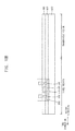
- FIG. 1 is a plan view illustrating an organic light emitting display device according to an exemplary embodiment.
- an organic light emitting display (OLED) device 100 may include a pixel region I and a transparent region II.
- a first sub-pixel 315, a second sub-pixel 320, and a third sub-pixel 325 may be located in the pixel region I, and a transparent window 370 may be located in the transparent region II.
- the first sub-pixel 315 may be a pixel emitting a red color and may extend along a first direction.
- the second sub-pixel 320 may be a pixel emitting a green color and may be disposed substantially parallel to the first sub-pixel 315.
- the third sub-pixel 325 may be a pixel emitting a blue color and may be disposed substantially parallel to the first sub-pixel 315 and the second sub-pixel 320.
- the first, second, and third sub-pixels 315, 320, and 325 may be located at the same level on a substrate.
- the first, second, and third sub-pixels 315, 320, and 325 may extend along the first direction because the first, second, and third sub-pixels 315, 320, and 325 are manufactured through a Small Mask Scanning (SMS) method.
- SMS Small Mask Scanning
- the transparent window 370 may transmit an external light.
- common lines i.e., data lines, scan lines, power supply lines, etc.
- insulating layers i.e., a pixel defining layer, a protection layer, etc.
- a pixel defining layer 310 may surround the first, second, and third sub-pixels 315, 320, and 325 and the transparent window 370.
- an upper electrode 330 of the OLED device 100 may be disposed on the first, second, and third sub-pixels 315, 320, and 325 in the pixel region I.
- the upper electrode 330 may extend along the first direction. In this case, the upper electrode 330 is not located in the transparent region II. Thus, the upper electrode 330 may expose the transparent region II.
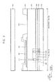
- FIG. 2 is a cross sectional view illustrating an organic light emitting display device taken along line III-III' of FIG. 1 .
- an organic light emitting display (OLED) device 100 may include a substrate 110, a first insulating layer 150, a second insulating layer 190, a third insulating layer 270, a driving transistor 250, a lower electrode 290, a pixel defining layer 310, a light emitting layer of first sub-pixel 315 (equally applicable to the light emitting layers of the other sub-pixels 320 and 325), an upper electrode 330, a transparent window 370, and an encapsulation substrate 350.
- the driving transistor 250 may include an active layer 130, a gate electrode 170, a source electrode 210, and a drain electrode 230.
- the OLED device 100 may include a pixel region I and a transparent region II.
- the driving transistor 250, the lower electrode 290, the light emitting layer of first sub-pixel 315, and the upper electrode 330 may be located in the pixel region I.
- the transparent window 370 may be located in the transparent region II.
- a display image may be displayed in the pixel region I.
- An image of an object that is located in the rear of the OLED device 100 may be transmitted in the transparent region II. Because the OLED device 100 has the transparent region II, the OLED device 100 may serve as a transparent display device.
- the substrate 110 may include transparent materials.
- the substrate 110 may include quartz, synthetic quartz, calcium fluoride, fluoride-doping quartz, a soda lime glass, and a non-alkali glass.
- the substrate 110 may include any other suitable material.
- the substrate 110 may include a flexible transparent resin substrate.
- the flexible transparent resin substrate for the substrate 110 may include a polyimide substrate.
- the polyimide substrate may include a first polyimide layer, a barrier film layer, and a second polyimide layer.
- the polyimide substrate may be formed on a rigid glass substrate to help support the formation of an upper structure (e.g., the driving transistor 250, the lower electrode 290, the light emitting layer of first sub-pixel 315, and the upper electrode 330).
- the substrate 110 may have a structure that includes the first polyimide layer, the barrier film layer, and the second polyimide layer stacked on a glass substrate.
- the upper structure may be disposed on the insulation layer.
- the glass substrate may be removed. It may be difficult to directly form the upper structure on the polyimide substrate because the polyimide substrate is thin and flexible.
- the upper structure is formed on a rigid glass substrate, and then the polyimide substrate may serve as the substrate 110 after the removal of the glass substrate. Because the OLED device 100 includes the pixel region I and the transparent region II, the substrate 110 may also include the pixel region I and the transparent region II.
- the buffer layer (not shown) may be disposed on the substrate 110.
- the buffer layer may extend from the pixel region I into the transparent region II.
- the buffer layer may prevent the diffusion of metal atoms and/or impurities from the substrate 110.
- the buffer layer may control a rate of heat transfer in a crystallization process for forming an active layer 130, thereby obtaining a substantially uniform active layer 130.
- the buffer layer may improve surface flatness of the substrate 110 when a surface of the substrate 110 is relatively irregular.
- the buffer layer may include at least one of silicon nitride and silicon oxide.
- the buffer layer may include any other suitable material.
- at least two buffer layers may be provided on the substrate 110.
- the buffer layer is not disposed on the substrate 110.
- the driving transistor 250 may include the active layer 130, the gate electrode 170, the source electrode 210, and the drain electrode 230.
- the active layer 130 may be disposed on the substrate 110.
- the active layer 130 may include at least one of an oxide semiconductor, an inorganic semiconductor (i.e., amorphous silicon, polysilicon, etc.), and an organic semiconductor.
- the active layer 130 may include any other suitable material.
- the first insulating layer 150 may be disposed on the active layer 130.
- the first insulating layer 150 may cover the active layer 130 in the pixel region I, and may extend into the transparent region II. Thus, the first insulating layer 150 may be entirely disposed in the pixel region I and the transparent region II of the substrate 110.
- the first insulating layer 150 may include at least one of a silicon compound and a metal oxide.
- the first insulating layer 150 may include any other suitable material.
- the gate electrode 170 may be disposed on the first insulating layer 150 directly over the active layer 130, which is located under the first insulating layer 150.
- the gate electrode 170 may include at least one of metal, metal alloy, metal nitride, conductive metal oxide, and transparent conductive materials.
- the gate electrode 170 may include any other suitable material.
- the second insulating layer 190 may be disposed on the gate electrode 170.
- the second insulating layer 190 may cover the gate electrode 170 in the pixel region I and may extend into the transparent region II.
- the second insulating layer 190 may be entirely disposed in the pixel region I and the transparent region II of the substrate 110.
- the second insulating layer 190 may include at least one of a silicon compound and a metal oxide.
- the second insulating layer 190 may include any other suitable material.
- the source electrode 210 and the drain electrode 230 may be disposed on the second insulating layer 190.
- the source electrode 210 may contact a first side of the active layer 130 by removing a portion of the first and second insulating layer 150 and 190.
- the drain electrode 230 may contact a second side of the active layer 130 by removing a second portion of the first and second insulating layer 150 and 190.
- Each of the source electrode 210 and the drain electrode 230 may include at least one of metal, metal alloy, metal nitride, conductive metal oxide, and transparent conductive materials.
- the source electrode 210 and the drain electrode 230 may include any other suitable material.
- the third insulating layer 270 may be disposed on the source electrode 210 and the drain electrode 230.
- the third insulating layer 270 may cover the source electrode 210 and the drain electrode 230 in the pixel region I, and may extend into the transparent region II.
- the third insulating layer 270 may be entirely disposed in the pixel region I and the transparent region II of the substrate 110.
- the third insulating layer 270 may include at least one of a silicon compound and a metal oxide.
- the third insulating layer 270 may include any other suitable material.
- the lower electrode 290 may be disposed on the third insulating layer 270.
- the lower electrode 290 may contact the source electrode 210 by removing a portion of the third insulating layer 270.
- the lower electrode 290 may include at least one of metal, metal alloy, metal nitride, conductive metal oxide, and transparent conductive materials.
- the pixel defining layer 310 may be disposed the on third insulating layer 270 to expose a portion of the lower electrode 290.
- the pixel defining layer 310 may include at least one of organic materials and inorganic materials.
- the pixel defining layer 310 may include a first opening and a second opening.
- the first opening of the pixel defining layer 310 may expose a portion of the lower electrode 290.
- the light emitting layer of first sub-pixel 315 may be disposed on the exposed lower electrode 290.
- the second opening of the pixel defining layer 310 may expose a portion of the third insulating layer 270.
- the second opening may be the transparent window 370.
- the second opening is not disposed on the third insulating layer 270, and the transparent region II may be the transparent window 370.
- the pixel defining layer 310 may have a plan upper surface in the transparent region II.
- the light emitting layer of first sub-pixel 315 may be disposed on the exposed lower electrode 290.
- the light emitting layer of first sub-pixel 315 may be formed using light emitting materials capable of generating different colors of light (e.g., a red color of light, a blue color of light, and a green color of light) according to the first, second, and third sub-pixels 315, 320, and 325 illustrated in FIG. 1 .
- the light emitting layer of first sub-pixel 315 illustrated in FIG. 2 may be formed using the light emitting material capable of generating the red color of light.
- the upper electrode 330 may be disposed on the pixel defining layer 310 and the light emitting layer of first sub-pixel 315 in the pixel region I.
- the upper electrode 330 is not located in the transparent region II.
- the upper electrode 330 may expose the transparent region II.
- the upper electrode 330 may be shared by the first, second, and third sub-pixels 315, 320, and 325 (shown in FIG. 1 ).
- the upper electrode 330 may be relatively thick.
- a thickness of the upper electrode 330 may be over about 10 nm (100 ⁇ , angstrom). In this case, a light transmissivity of the upper electrode 330 may be below about 50%.
- the upper electrode 330 may include at least one of metal, metal alloy, metal nitride, conductive metal oxide, and a transparent conductive material.
- the upper electrode 330 may include at least one of aluminum (Al), aluminum alloy, aluminum nitride (AlNx), silver (Ag), silver alloy, tungsten (W), tungsten nitride (WNx), copper (Cu), copper alloy, nickel (Ni), chrome (Cr), chrome nitride (CrNx), molybdenum (Mo), molybdenum alloy, magnesium (Mg), magnesium alloy, magnesium-silver (Mg-Ag) alloy, titanium (Ti), titanium nitride (TiNx), platinum (Pt), tantalum (Ta), tantalum nitride (TaNx), neodymium (Nd), scandium (Sc), strontium ruthenium oxide (SRO), zinc oxide (ZnOx), aluminum zinc oxide (AZO), indium tin oxide
- the upper electrode 330 may use any other suitable material as well.
- the upper electrode 330 may include magnesium-silver (Mg-Ag) alloy.
- the OLED device 100 includes the relatively thick upper electrode 330, resulting in a reduced generation of IR drop (i.e., voltage drop) in the OLED device 100. Accordingly, a uniform luminance may be provided in the OLED device 100.
- the transmissivity of the OLED device 100 may be increased.
- a definition (e.g., visibility) of an image of an object that is located in the rear (e.g., at the back) of the OLED device 100 may be increased.
- the encapsulation substrate 350 may be disposed on the upper electrode 330, pixel defining layer 310, and the transparent window 370.
- the encapsulation substrate 350 and the substrate 110 may include substantially the same materials.
- the encapsulation substrate 350 may include at least one of quartz, synthetic quartz, calcium fluoride, fluoride-doping quartz, soda lime glass, and non-alkali glass.
- the encapsulation substrate 350 may include any other suitable material.
- the encapsulation substrate 350 may include at least one of a transparent inorganic material and a flexible plastic.
- the encapsulation substrate 350 may include a flexible transparent resin substrate.
- the encapsulation substrate 350 may include a stacked structure where at least one organic layer and at least one inorganic layer are alternately stacked.
- the first insulating layer 150, the second insulating layer 190, and the third insulating layer 270 have the same materials, and the substrate 110, the encapsulation substrate 350, the first insulating layer 150, the second insulating layer 190, and the third insulating layer 270 have a same (or similar) refractive index, a light incident into the transparent region II is not refracted by the interfaces of the substrate 110, the encapsulation substrate 350, the first insulating layer 150, the second insulating layer 190, and the third insulating layer 270. Accordingly, the transmissivity of the OLED device 100 may be increased, and the definition of the image may be improved.
- the OLED device 100 includes the relatively thick upper electrode 330, which may only be located in the pixel region I. Accordingly, the OLED device 100 may serve as a transparent display device with improved transmissivity. In addition, because the upper electrode 330 is not located in the transparent region II, the OLED device 100 may have increased transmissivity. The OLED device 100 may have an increased definition of the image of the object that is located in the rear of the OLED device 100. Further, when the first insulating layer 150, the second insulating layer 190, and the third insulating layer 270 include the same materials, the OLED device 100 may have a decrease in contact interfaces capable of reflecting a light. Thus, the resulting OLED 100 may have an increased transmissivity and definition of the image of the object that is located in the rear of the OLED device 100.
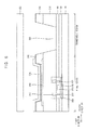
- FIG. 3 is a cross sectional view illustrating an organic light emitting display device according to an exemplary embodiment.
- An organic light emitting display device illustrated in FIG. 3 may have a configuration substantially similar the organic light emitting display device 100 described with reference to FIG. 2 except for a shape of transparent window 375.
- FIG. 3 detailed descriptions for elements that are substantially similar to the elements described with reference to FIG. 2 will be omitted for brevity.
- an organic light emitting display (OLED) device may include at least one of a substrate 110, a first insulating layer 150, a second insulating layer 190, a third insulating layer 270, a driving transistor 250, a lower electrode 290, a pixel defining layer 310, a light emitting layer of first sub-pixel 315, an upper electrode 330, a transparent window 375, and an encapsulation substrate 350.
- the driving transistor 250 may include an active layer 130, a gate electrode 170, a source electrode 210, and a drain electrode 230.
- the OLED device may include a pixel region I and a transparent region II.
- the driving transistor 250, the lower electrode 290, the light emitting layer of first sub-pixel 315, and the upper electrode 330 may be located in the pixel region I.
- the transparent window 375 may be located in the transparent region II.
- a display image may be displayed in the pixel region I.
- An image of an object that is located in the rear of the OLED device may be transmitted in the transparent region II. Accordingly, the OLED device having the transparent region II may serve as a transparent display device.
- the pixel defining layer 310 may be disposed on the third insulating layer 270 to expose a portion of the lower electrode 290.
- the pixel defining layer 310 may include at least one of organic materials and inorganic materials.
- the pixel defining layer 310 may include a first opening and a second opening.
- the first opening of the pixel defining layer 310 may expose a portion of the lower electrode 290.
- the light emitting layer of first sub-pixel 315 may be disposed on the exposed lower electrode 290.
- the second opening of the pixel defining layer 310 may expose a portion of the third insulating layer 270.
- the second opening of the pixel defining layer 310 may extend through the third insulating layer 270, the second insulating 190, and the first insulating layer.
- the second opening may be the transparent window 375.
- the transparent window 375 may be formed by removing a portion of the first insulating layer 150, a portion of the second insulating layer 190, a portion of the third insulating layer 270, and a portion of the pixel defining layer 310.
- portions of the insulating layers are not located in the transparent region II. In other words, the insulating layers may expose the transparent region II. In an alternate embodiment, at least one insulating layer may be located in the entire transparent region II.
- the OLED device may have an increased definition of an image of an object that is located in the rear of the OLED device.
- FIG. 4 is a plan view illustrating an organic light emitting display device according to an exemplary embodiment.
- An organic light emitting display device 300 illustrated in FIG. 4 may have a configuration substantially similar to an organic light emitting display device 100 described with reference to FIG. 1 except for an auxiliary electrode 340.
- FIG. 4 detailed descriptions for elements that are substantially similar to the elements described with reference to FIG. 1 will be omitted for brevity.
- an organic light emitting display (OLED) device 300 may include a pixel region I and a transparent region II.
- a first sub-pixel; 315, a second sub-pixel 320, and a third sub-pixel325 may be located in a pixel region I and a transparent window 380 may be located in the transparent region II.
- an auxiliary electrode 340 may be entirely located on the substrate 110 in the pixel region I and the transparent region II.
- the first sub-pixel 315 may be a pixel emitting a red color and may extend along a first direction.
- the second sub-pixel 320 may be a pixel emitting a green color and may be disposed substantially parallel to the first sub-pixel 315.
- the third sub-pixel 325 may be a pixel emitting a blue color and may be disposed substantially parallel to the first sub-pixel 315 and the second sub-pixel 320.
- the first, second, and third sub-pixels 315, 320, and 325 may be located at the same level on a substrate.
- the first, second, and third sub-pixels 315, 320, and 325 may extend along the first direction because the first, second, and third sub-pixels 315, 320, and 325 are manufactured through an SMS method.
- the transparent window 380 may transmit an external light.
- common lines and insulating layers may be disposed in a portion that surrounds the first, second, and third sub-pixels 315, 320, and 325 and the transparent window 380.
- a pixel defining layer 310 may surround the first, second, and third sub-pixels 315, 320, and 325 and the transparent window 380.
- an upper electrode 335 of the OLED device 300 may be disposed on the first, second, and third sub-pixels 315, 320, and 325 in the pixel region I and may extend along the first direction.
- the upper electrode 335 is not located in the transparent region II.
- the upper electrode 335 may expose the transparent region II.
- the auxiliary electrode 340 may be interposed between the upper electrode 335 and the first, second, and third sub-pixels 315, 320, and 325 and may extend along the first direction.
- the auxiliary electrode 340 may be located in the transparent region II.
- the auxiliary electrode 340 may be disposed in the same chamber as the first, second, and third sub-pixels 315, 320, and 325 after the first, second, and third sub-pixels 315, 320, and 325 are disposed. Then, an upper electrode 335 may be obtained through a Fine Metal Mask (FMM) method.
- FMM Fine Metal Mask
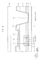
- FIG. 5 is a cross sectional view illustrating an organic light emitting display device taken along a line IV-IV' of FIG. 4 .
- An organic light emitting display device 300 illustrated in FIG. 5 may have a configuration substantially similar to organic light emitting display device 100 described with reference to FIG. 2 except for an auxiliary electrode 340.
- FIG. 5 detailed descriptions for elements, which are substantially to the elements described with reference to FIG. 2 , will be omitted for brevity.
- an organic light emitting display (OLED) device 300 may include a substrate 110, a first insulating layer 150, a second insulating layer 190, a third insulating layer 270, a driving transistor 250, a lower electrode 290, a pixel defining layer 310, a light emitting layer of first sub-pixel 315, an upper electrode 335, an auxiliary electrode 340, a transparent window 380, and an encapsulation substrate 350.
- the driving transistor 250 may include an active layer 130, a gate electrode 170, a source electrode 210, and a drain electrode 230.
- the OLED device 300 may include a pixel region I and a transparent region II.
- the driving transistor 250, the lower electrode 290, the light emitting layer of first sub-pixel 315, and the upper electrode 335 may be located in the pixel region I.
- the transparent window 380 may be located in the transparent region II.
- the auxiliary electrode 340 may be entirely located on the substrate 110 in the pixel region I and the transparent region II. For example, a display image may be displayed in the pixel region I. An image of an object that is located in the rear of the OLED device 300 may be transmitted in the transparent region II. Because the OLED device 300 has the transparent region II, the OLED device 300 may serve as a transparent display device.
- the pixel defining layer 310 may be disposed on the third insulating layer 270 to expose a portion of the lower electrode 290.
- the pixel defining layer 310 may include at least one of organic materials and inorganic materials.
- the pixel defining layer 310 may include a first opening and a second opening.
- the first opening of the pixel defining layer 310 may expose a portion of the lower electrode 290.
- the light emitting layer of first sub-pixel 315 may be disposed on the exposed lower electrode 290.
- the second opening of the pixel defining layer 310 may expose a portion of the third insulating layer 270.
- the second opening may be the transparent window 380.
- the light emitting layer of first sub-pixel 315 may be disposed on the exposed lower electrode 290.
- the light emitting layer of first sub-pixel 315 may be formed using light emitting materials capable of generating different colors of light (e.g., a red color of light, a blue color of light, and a green color of light) according to the first, second, and third sub-pixels 315, 320, and 325 illustrated in FIG. 1 .
- the light emitting layer of first sub-pixel 315 illustrated in FIG. 5 may be formed using the light emitting material capable of generating the red color of light.
- the auxiliary electrode 340 may be disposed on the pixel defining layer 310, the light emitting layer of first sub-pixel 315, and a portion of the third insulating layer 270.
- the auxiliary electrode 340 may cover the pixel defining layer 310 and the light emitting layer of first sub-pixel 315 and may extend into the transparent region II in a second direction that is substantially perpendicular to the first direction.
- the auxiliary electrode 340 may be located in the transparent region II.
- the auxiliary electrode 340 may be shared by the first, second, and third sub-pixels 315, 320, and 325. Compared to the upper electrode 335, the auxiliary electrode 340 may be relatively thin.
- a thickness of the auxiliary electrode 340 may be below about 7.5 nm (75 ⁇ , angstrom). In this case, a light transmissivity of the auxiliary electrode 340 may be over about 50%.
- the auxiliary electrode 340 may include at least one of metal, metal alloy, metal nitride, conductive metal oxide, and a transparent conductive material.
- the auxiliary electrode 340 may include at least one of aluminum (Al), aluminum alloy, aluminum nitride (AlNx), silver (Ag), silver alloy, tungsten (W), tungsten nitride (WNx), copper (Cu), copper alloy, nickel (Ni), chrome (Cr), chrome nitride (CrNx), molybdenum (Mo), molybdenum alloy, magnesium (Mg), magnesium alloy, magnesium-silver (Mg-Ag) alloy, titanium (Ti), titanium nitride (TiNx), platinum (Pt), tantalum (Ta), tantalum nitride (TaNx), neodymium (Nd), scandium (Sc), strontium ruthenium oxide (SRO), zinc oxide (ZnOx), aluminum zinc oxide (AZO), indium tin oxide (ITO), stannum oxide (SnOx), indium oxide (InOx), indium tin oxide (ITO), gallium oxide
- the upper electrode 335 may be disposed on the auxiliary electrode 340 in the pixel region I.
- the upper electrode 335 may electrically contact the auxiliary electrode 340.
- the upper electrode 335 is not located in the transparent region II. That is, the upper electrode 335 may expose the transparent region II.
- the upper electrode 335 may be shared by the first through third sub-pixels 315, 320, and 325.
- the upper electrode 335 may have a relatively thick thickness.
- a thickness of the upper electrode 335 may be over about 100 um.
- a light transmissivity of the upper electrode 335 may be below about 50%.
- the upper electrode 335 may include at least one of metal, metal alloy, metal nitride, conductive metal oxide, and a transparent conductive material.
- the upper electrode 335 may include at least one of aluminum (Al), aluminum alloy, aluminum nitride (AlNx), silver (Ag), silver alloy, tungsten (W), tungsten nitride (WNx), copper (Cu), copper alloy, nickel (Ni), chrome (Cr), chrome nitride (CrNx), molybdenum (Mo), molybdenum alloy, magnesium (Mg), magnesium alloy, magnesium-silver (Mg-Ag) alloy, titanium (Ti), titanium nitride (TiNx), platinum (Pt), tantalum (Ta), tantalum nitride (TaNx), neodymium (Nd), scandium (Sc), strontium ruthenium oxide (SRO), zinc oxide (ZnOx), aluminum zinc oxide (AZO), indium tin oxide
- the upper electrode 335 may include Mg-Ag alloy.
- the OLED device 300 includes the relatively thick upper electrode 335 and the auxiliary electrode 340, resulting in a reduced generation of an IR drop in the OLED device 300.
- a uniform luminance may be provided in the OLED device 300.
- the relatively thin auxiliary electrode 340 is located in the transparent region II, the transmissivity of the OLED device 300 is not significantly decreased.
- FIG. 6 is a cross sectional view illustrating an organic light emitting display device according to an exemplary embodiment.
- An organic light emitting display device illustrated in FIG. 6 may have a configuration substantially similar to organic light emitting display device 300 described with reference to FIG. 5 except for a shape of an auxiliary electrode 345 and a transparent window 385.
- FIG. 6 detailed descriptions for elements that are substantially similar to the elements described with reference to FIG. 5 will be omitted for brevity.
- an organic light emitting display (OLED) device may include a substrate 110, a first insulating layer 150, a second insulating layer 190, a third insulating layer 270, a driving transistor 250, a lower electrode 290, a pixel defining layer 310, a light emitting layer of first sub-pixel 315, an upper electrode 335, an auxiliary electrode 345, a transparent window 385, and an encapsulation substrate 350.
- the driving transistor 250 may include an active layer 130, a gate electrode 170, a source electrode 210, and a drain electrode 230.
- the OLED device may include a pixel region I and a transparent region II.
- the driving transistor 250, the lower electrode 290, the light emitting layer of first sub-pixel 315, and the upper electrode 335 may be located in the pixel region I.
- the transparent window 385 may be located in the transparent region II.
- the auxiliary electrode 345 may be entirely located on the substrate 110 in the pixel region I.
- a display image may be displayed in the pixel region I.
- An image of an object that is located in the rear of the OLED device may be transmitted in the transparent region II. Accordingly, the OLED device having the transparent region II may serve as a transparent display device.
- the pixel defining layer 310 may be disposed on the third insulating layer 270 to expose a portion of the lower electrode 290.
- the pixel defining layer 310 may include at least one of organic material and inorganic materials.
- the pixel defining layer 310 may include a first opening and a second opening.
- the first opening of the pixel defining layer 310 may expose a portion of the lower electrode 290.
- the light emitting layer of first sub-pixel 315 may be disposed on the exposed lower electrode 290.
- the second opening of the pixel defining layer 310 may expose a portion of the third insulating layer 270.
- the second opening may also extend through the third insulating layer 270 exposing a portion of the second insulating layer 190.
- the second opening may be the transparent window 385.
- the transparent window 385 may be formed by removing a portion of the auxiliary electrode 345, a portion of the third insulating layer 270, and a portion of the pixel defining layer 310.
- portions of the third insulating layer 270, the pixel defining layer 310, and the auxiliary electrode 345 is not located in the transparent region II.
- at least one insulating layer and/or at least one electrode may be located in the entire transparent region II.
- a transmissivity of the transparent region II may further be substantially increased.
- the OLED device has the auxiliary electrode 345, resulting in a reduction of the generation of an IR drop in the OLED device.
- the OLED device may have an increased definition of an image of an object that is located in the rear of the OLED device.
- FIG. 7 is a cross sectional view illustrating an organic light emitting display device according to an exemplary embodiment.
- An organic light emitting display device illustrated in FIG. 7 may have a configuration substantially similar to organic light emitting display device 300 described with reference to FIG. 5 except for a shape of an upper electrode 355, an auxiliary electrode 360, and a transparent window 390.
- FIG. 7 detailed descriptions for elements that are substantially similar to the elements described with reference to FIG. 5 will be omitted for brevity.
- an organic light emitting display (OLED) device may include a substrate 110, a first insulating layer 150, a second insulating layer 190, a third insulating layer 270, a driving transistor 250, a lower electrode 290, a pixel defining layer 310, a light emitting layer of first sub-pixel 315, an upper electrode 355, an auxiliary electrode 360, a transparent window 390, and an encapsulation substrate 350.
- the driving transistor 250 may include an active layer 130, a gate electrode 170, a source electrode 210, and a drain electrode 230.
- the OLED device may include a pixel region I and a transparent region II.
- the driving transistor 250, the lower electrode 290, the light emitting layer of first sub-pixel 315, and the upper electrode 355 may be located in the pixel region I.
- the transparent window 390 may be located in the transparent region II.
- a display image may be displayed in the pixel region I.
- An image of an object that is located in the rear of the OLED device may be transmitted in the transparent region II. Accordingly the OLED device having the transparent region II may serve as a transparent display device.
- the pixel defining layer 310 may be disposed on the third insulating layer 270 to expose a portion of the lower electrode 290.
- the pixel defining layer 310 may include a first opening and a second opening.
- the first opening of the pixel defining layer 310 may expose a portion of the lower electrode 290.
- the light emitting layer of first sub-pixel 315 may be disposed on the exposed lower electrode 290.
- the second opening of the pixel defining layer 310 may expose a portion of the third insulating layer 270.
- the second opening may be the transparent window 390.
- the pixel defining layer 310 may include at least one of organic materials and inorganic materials.
- the upper electrode 355 may be disposed on the pixel defining layer 310 and light emitting layer of first sub-pixel 315 in the pixel region I.
- the upper electrode 355 is not located in the transparent region II.
- the upper electrode 355 may expose the transparent region II.
- the upper electrode 355 may be relatively thick.
- a thickness of the upper electrode 355 may be over about 10 nm (100 ⁇ , angstrom).
- a light transmissivity of the upper electrode 355 may be below about 50%.
- the upper electrode 355 may include at least one of metal, metal alloy, metal nitride, conductive metal oxide, and a transparent conductive material.
- the upper electrode 355 may include at least one of aluminum (Al), aluminum alloy, aluminum nitride (AlNx), silver (Ag), silver alloy, tungsten (W), tungsten nitride (WNx), copper (Cu), copper alloy, nickel (Ni), chrome (Cr), chrome nitride (CrNx), molybdenum (Mo), molybdenum alloy, magnesium (Mg), magnesium alloy, magnesium-silver (Mg-Ag) alloy, titanium (Ti), titanium nitride (TiNx), platinum (Pt), tantalum (Ta), tantalum nitride (TaNx), neodymium (Nd), scandium (Sc), strontium ruthenium oxide (SRO), zinc oxide (ZnOx), aluminum zinc oxide (AZO), indium tin oxide (ITO), stannum oxide (SnOx), indium oxide (InOx), indium tin oxide (ITO), gallium oxide (Ga
- the auxiliary electrode 360 may be disposed on the upper electrode 355 and a portion of pixel defining layer 310.
- the auxiliary electrode 360 may cover the upper electrode 355 and a portion of the pixel defining layer 310.
- a portion of auxiliary electrode 360 is not located in the transparent region II.
- the auxiliary electrode 360 may expose the transparent region II.
- the auxiliary electrode 360 may be relatively thin.
- a thickness of the auxiliary electrode 360 may be below about 7.5 nm (75 ⁇ , angstrom).
- a light transmissivity of the auxiliary electrode 360 may be over about 50%.
- the auxiliary electrode 360 may include at least one of metal, metal alloy, metal nitride, conductive metal oxide, and a transparent conductive material.
- the auxiliary electrode 360 may include at least one of aluminum (Al), aluminum alloy, aluminum nitride (AlNx), silver (Ag), silver alloy, tungsten (W), tungsten nitride (WNx), copper (Cu), copper alloy, nickel (Ni), chrome (Cr), chrome nitride (CrNx), molybdenum (Mo), molybdenum alloy, magnesium (Mg), magnesium alloy, magnesium-silver (Mg-Ag) alloy, titanium (Ti), titanium nitride (TiNx), platinum (Pt), tantalum (Ta), tantalum nitride (TaNx), neodymium (Nd), scandium (Sc), strontium ruthenium oxide (SRO), zinc oxide (ZnOx), aluminum zinc oxide (AZO), indium tin oxide
- the OLED device of the exemplary embodiment includes the relatively thick upper electrode 355 and the relatively thin auxiliary electrode 360, resulting in a reduction of the generation of an IR in the OLED device.
- the auxiliary electrode 360 is not located in a portion of the transparent region II, a transmissivity of the transparent region II may further be substantially increased.
- an OLED device may have an increased definition of an image of an object that is located in the rear of the OLED device.
- FIG. 8 is a cross sectional view illustrating an organic light emitting display device according to an exemplary embodiment.
- An organic light emitting display device illustrated in FIG. 8 may have a configuration substantially similar to an organic light emitting display device described with reference to FIG. 7 except for a shape of an auxiliary electrode 365 and a transparent window 395.
- FIG. 8 detailed descriptions for elements, which are substantially the same as or similar to the elements described with reference to FIG. 7 , will be omitted.
- an organic light emitting display (OLED) device may include a substrate 110, a first insulating layer 150, a second insulating layer 190, a third insulating layer 270, a driving transistor 250, a lower electrode 290, a pixel defining layer 310, a light emitting layer of first sub-pixel 315, an upper electrode 355, an auxiliary electrode 365, a transparent window 395, and an encapsulation substrate 350.
- the driving transistor 250 may include an active layer 130, a gate electrode 170, a source electrode 210, and a drain electrode 230.
- the OLED device may include a pixel region I and a transparent region II.
- the driving transistor 250, the lower electrode 290, the light emitting layer of first sub-pixel 315, and the upper electrode 355 may be located in the pixel region I.
- the transparent window 395 may be located in the transparent region II.
- the auxiliary electrode 365 may be entirely located on the substrate 110 in the pixel region I. For example, a display image may be displayed in the pixel region I. An image of an object that is located in the rear of the OLED device may be transmitted in the transparent region II. Accordingly, the OLED device having the transparent region II may serve as a transparent display device.
- the pixel defining layer 310 may be disposed on a portion of the third insulating layer 270 and a portion of the lower electrode 290.
- the pixel defining layer 310 may include a first opening and a second opening.
- the first opening of the pixel defining layer 310 may be located on a portion of the lower electrode 290 disposed on the third insulating layer 270.
- the light emitting layer of first sub-pixel 315 may be disposed in the first opening on the lower electrode 290.
- the second opening of the pixel defining layer 310 may be located in the transparent region II.
- the second opening may be the transparent window 395.
- the pixel defining layer 310 may include at least one of organic materials and inorganic materials.
- the transparent window 395 may be formed by removing a portion of the first insulating layer 150, a portion of the second insulating layer 190, a portion of the third insulating layer 270, and a portion of the pixel defining layer 310.
- portions of the insulating layers, 150, 190, and 270 are not located in the transparent region II.
- the insulating layers 150, 190, and 270 may expose the transparent region II.
- the OLED device may result in a substantially increased transmissivity of the transparent region II.
- at least one insulating layer may be located in the entire transparent region II.
- the upper electrode 355 may be disposed on the pixel defining layer 310 and light emitting layer of first sub-pixel 315 in the pixel region I.
- the upper electrode 355 is not located in the transparent region II. In other words, the upper electrode 355 may expose the transparent region II.
- the upper electrode 355 may be relatively thick. A thickness of the upper electrode 355 may be over about 10 nm (100 ⁇ , angstrom). For example, a light transmissivity of the upper electrode 355 may be below about 50%.
- the upper electrode 355 may include at least one of metal, metal alloy, metal nitride, conductive metal oxide, and a transparent conductive material.
- the upper electrode 355 may also include any other suitable material. In an exemplary embodiment, the upper electrode 355 may include Mg-Ag alloy.
- the auxiliary electrode 365 may be disposed on a portion of the pixel defining layer 310 and a portion of the substrate 110. In other words, the auxiliary electrode 365 may be entirely located on the substrate 110 in the pixel region I and the transparent region II. Compared to the upper electrode 355, the auxiliary electrode 365 may be relatively thin. A thickness of the auxiliary electrode 365 may be below about 7.5 nm (75 ⁇ , angstrom). For example, a light transmissivity of the auxiliary electrode 365 may be over about 50%.
- the auxiliary electrode 365 may include at least one of metal, metal alloy, metal nitride, conductive metal oxide, and a transparent conductive material.
- the auxiliary electrode 365 may include at least one of aluminum (Al), aluminum alloy, aluminum nitride (AlNx), silver (Ag), silver alloy, tungsten (W), tungsten nitride (WNx), copper (Cu), copper alloy, nickel (Ni), chrome (Cr), chrome nitride (CrNx), molybdenum (Mo), molybdenum alloy, magnesium (Mg), magnesium alloy, magnesium-silver (Mg-Ag) alloy, titanium (Ti), titanium nitride (TiNx), platinum (Pt), tantalum (Ta), tantalum nitride (TaNx), neodymium (Nd), scandium (Sc), strontium ruthenium oxide (SRO), zinc oxide (ZnOx), aluminum zinc oxide (AZO), indium tin oxide (ITO), stannum oxide (SnOx), indium oxide (InOx), indium tin oxide (ITO), gallium oxide (G
- the OLED device has the auxiliary electrode 365 that is entirely disposed on the substrate 110 in the pixel region I and the transparent region II, the OLED device may have a reduction in the generation of an IR drop.
- the auxiliary electrode 365 is relatively thin and is located in the transparent region II, the OLED device may not suffer from a significant decrease in the transmissivity of the OLED device.
- FIG. 9 is a plan view illustrating an organic light emitting display device according to an exemplary embodiment.
- An organic light emitting display device illustrated in FIG. 9 may have a configuration substantially similar to an organic light emitting display device 300 described with reference to FIG. 4 except for a fourth sub-pixel.
- FIG. 9 detailed descriptions for elements that are substantially similar to the elements described with reference to FIG. 4 will be omitted for brevity.
- an organic light emitting display (OLED) device may include a pixel region I and a transparent region II.
- a first sub-pixel 315, a second sub-pixel 320, a third sub-pixel 325, and a fourth sub-pixel 327 may be located in a pixel region I.
- a transparent window 380 may be located in the transparent region II.
- an auxiliary electrode 340 may be entirely located on the substrate 110 in the pixel region I and the transparent region II.
- the first sub-pixel 315 may be a pixel emitting a red color and may extend along a first direction.
- the second sub-pixel 320 may be a pixel emitting a green color and may be disposed substantially parallel to the first sub-pixel 315.
- the third sub-pixel 325 may be a pixel emitting a blue color and may be disposed substantially parallel to the first sub-pixel 315 and the second sub-pixel 320.
- the fourth sub-pixel 327 may be a pixel emitting a white color and may be disposed substantially parallel to the first, second, and third sub-pixels 315, 320, and 325.
- the first, second, third, and fourth sub-pixels 315, 320, 325, and 327 may be located at the same level on a substrate.
- the first, second, third, and fourth sub-pixels 315, 320, 325, and 327 may extend along the first direction because the first, second, third, and fourth sub-pixels 315, 320, 325, and 327 are manufactured through an SMS method.
- the transparent window 380 may transmit an external light in the transparent region II.
- common lines and insulating layers may be disposed in a portion that surrounds the first, second, third, and fourth sub-pixels 315, 320, 325, and 327 and the transparent window 380.
- a pixel defining layer 310 may surround the first, second, third, and fourth sub-pixels 315, 320, 325, and 327 and the transparent window 380.
- the upper electrode 335 may be disposed on the first, second, third, and fourth sub-pixels 315, 320, 325, and 327 in the pixel region I and may extend along the first direction.
- the upper electrode 335 is not located in the transparent region II.
- the upper electrode 335 may expose the transparent region II.
- the auxiliary electrode 340 may be disposed between the upper electrode 335 and the first, second, third, and fourth sub-pixels 315, 320, 325, and 327 and may extend along the first direction and second direction. In other words, the auxiliary electrode 340 may be located in the pixel region I and the transparent region II.
- the auxiliary electrode 340 may be disposed directly on the upper electrode 335 (instead of between the upper electrode 335 and the first, second, third, and fourth sub-pixels 315, 320, 325, and 327) and may extend along the first direction and the second direction.
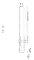
- FIGS. 10A , 10B , 10C , 10D , 10E , and 10F are cross sectional views illustrating a method of manufacturing an organic light emitting display device according to an exemplary embodiment.
- an active layer 830 may be formed in a pixel region I of a substrate 810.
- the substrate 810 may be formed using at least one of quartz, synthetic quartz, calcium fluoride, fluoride-doping quartz, a soda lime glass, and a non-alkali glass.
- the substrate 810 may also be formed using any other suitable material.
- a buffer layer may be formed on the substrate 810.
- the buffer layer may be entirely formed from the pixel region I into the transparent region II any may cover the entire pixel region I and transparent region II.
- the buffer layer may prevent the diffusion of metal atoms and/or impurities from the substrate 810 into other layers and components of the OLED device (e.g., the active layer 830).
- the active layer 830 may be formed on the substrate 810 in the pixel region I.
- the active layer 830 may be formed using at least one of an oxide semiconductor, an inorganic semiconductor, and an organic semiconductor.
- the active layer 830 may include any other suitable material.
- a first insulating layer 850 may be formed on the substrate 810.
- the first insulating layer 850 may cover the active layer 830 and may extend from the transparent region II.
- the first insulating layer 850 may be entirely formed on the substrate 810 in the pixel region I and the transparent region II.
- the first insulating layer 850 may be formed using at least one of a silicon compound and a metal oxide.
- a gate electrode 870 may be formed on the first insulating layer 850 over the active layer 830, which is located under the first insulating layer 850.
- the gate electrode 870 may be formed using at least one of metal, metal alloy, metal nitride, conductive metal oxide, and transparent conductive materials.
- the gate electrode 870 may also be
- a second insulating layer 890 may be formed on the gate electrode 870.
- the second insulating layer 890 may cover the gate electrode 870 and may extend from the transparent region II.
- the second insulating layer 890 may be entirely formed on the substrate 810 in the pixel region I and the transparent region II.
- the second insulating layer 890 may be formed using at least one of a silicon compound and a metal oxide.
- the second insulating layer 890 may be form of any other suitable material.
- a source electrode 910 and a drain electrode 930 may be formed on the second insulating layer 890.
- the source electrode 910 may contact a first side of the active layer 830 by removing a first portion of the first and second insulating layers 850 and 890 and the drain electrode 930 may contact a second side of the active layer 830 by removing a second portion of the first and second insulating layers 850 and 890.
- Each of the source electrode 910 and the drain electrode 930 may be formed using at least one of metal, metal alloy, metal nitride, conductive metal oxide, and transparent conductive materials.
- Each of the source electrode 90 and the drain electrode 930 may be formed using any other suitable material.
- a driving transistor 950 having the source electrode 910, the drain electrode 930, the gate electrode 870, and the active layer 830 may be formed.
- a lower electrode 990 may be formed on a third insulating layer 970.
- the lower electrode 990 may contact the source electrode 910 by removing a portion of the third insulating layer 970.
- the lower electrode 990 may be formed using at least one of metal, metal alloy, metal nitride, conductive metal oxide, and transparent conductive materials.
- the lower electrode 990 may be formed using any other suitable material.
- the pixel defining layer 1010 may be formed on a portion of third insulating layer 970 and a portion of the lower electrode 990.
- the pixel defining layer 1010 may include a first opening.
- the first opening of the pixel defining layer 1010 may be in the pixel region I exposing a portion of the lower electrode 990 and formed on the third insulating layer 970 and a portion of the lower electrode 990.
- the pixel defining layer 1010 may be formed using at least one of organic materials and inorganic materials.
- a light emitting layer 1015 may be formed in the first opening of the pixel defining layer 1010.
- the light emitting layer 1015 may be formed on the lower electrode 990.
- the light emitting layer 1015 may be formed using at least one of light emitting materials capable of generating different colors of light.
- the light emitting layer 1015 may be formed through an SMS method.
- the light emitting layer 1015 may extend along the first direction.
- An auxiliary electrode 1080 may be formed on the pixel defining layer 1010 and light emitting layer 1015.
- the auxiliary electrode 1080 may cover the pixel defining layer 1010 and the light emitting layer 1015 and extend along the first direction and a second direction (e.g., a direction from the pixel region I into the transparent region II) that is substantially perpendicular to the first direction.
- the auxiliary electrode 1080 may be formed through the SMS method. Because the auxiliary electrode 1080 is formed through the SMS method, the auxiliary electrode 1080 may be formed in the same chamber as the light emitting layer 1015 but may be formed after the light emitting layer 1015. Accordingly, manufacturing cost and time may be relatively reduced.
- the auxiliary electrode 1080 may be relatively thin. For example, a thickness of the auxiliary electrode 1080 may be formed below about 7.5 nm (75 ⁇ , angstrom). A light transmissivity of the auxiliary electrode 1080 may be over about 50%. The auxiliary electrode 1080 may be entirely formed in the pixel region I and the transparent region II.
- the auxiliary electrode 1080 may include at least one of metal, metal alloy, metal nitride, conductive metal oxide, and a transparent conductive material.
- the auxiliary electrode 1080 may be formed using at least one of aluminum (Al), aluminum alloy, aluminum nitride (AlNx), silver (Ag), silver alloy, tungsten (W), tungsten nitride (WNx), copper (Cu), copper alloy, nickel (Ni), chrome (Cr), chrome nitride (CrNx), molybdenum (Mo), molybdenum alloy, magnesium (Mg), magnesium alloy, magnesium-silver (Mg-Ag) alloy, titanium (Ti), titanium nitride (TiNx), platinum (Pt), tantalum (Ta), tantalum nitride (TaNx), neodymium (Nd), scandium (Sc), strontium ruthenium oxide (SRO), zinc oxide (ZnOx), aluminum zinc oxide (AZO), indium tin oxide (ITO), stannum oxide (SnOx), indium oxide (InOx), indium tin oxide (ITO), gallium gall
- the upper electrode 1075 may be formed on the auxiliary electrode 1080 in the pixel region I.
- the upper electrode 1075 may electrically contact the auxiliary electrode 1080.
- the upper electrode 1075 is not located in the transparent region II.
- the upper electrode 1075 may expose the transparent region II.
- the upper electrode 1075 may cover a portion of the auxiliary electrode 1080.
- the upper electrode 1075 may be formed through an FMM method. Because the upper electrode 1075 is formed through the FMM method, the upper electrode 1075 may be formed using a different chamber than the auxiliary electrode 1080 and may be formed after the auxiliary electrode 1080.
- the upper electrode 1075 may be relatively thick. For example, a thickness of the upper electrode 1075 may be formed over about 10 nm (100 ⁇ , angstrom). A light transmissivity of the upper electrode 1075 may be below about 50%.
- the upper electrode 1075 may be formed using at least one of metal, metal alloy, metal nitride, conductive metal oxide, and a transparent conductive material.
- the upper electrode 1075 may include at least one of aluminum (Al), aluminum alloy, aluminum nitride (AlNx), silver (Ag), silver alloy, tungsten (W), tungsten nitride (WNx), copper (Cu), copper alloy, nickel (Ni), chrome (Cr), chrome nitride (CrNx), molybdenum (Mo), molybdenum alloy, magnesium (Mg), magnesium alloy, magnesium-silver (Mg-Ag) alloy, titanium (Ti), titanium nitride (TiNx), platinum (Pt), tantalum (Ta), tantalum nitride (TaNx), neodymium (Nd), scandium (Sc), strontium ruthenium oxide (SRO), zinc oxide (ZnOx), aluminum zinc oxide (AZO), indium tin oxide (ITO), stannum oxide (SnOx), indium oxide (InOx), indium tin oxide (ITO), gallium oxide (Ga
- a second opening of the pixel defining layer 1010 may be located in the transparent region II.
- the second opening may be the transparent window 1070.
- the transparent window 1070 may be formed by removing a portion of the auxiliary electrode 1080, a portion of the first insulating layer 850, a portion of the second insulating layer 890, a portion of the third insulating layer 970, and a portion of the pixel defining layer 1010.
- An encapsulation substrate 1050 may be formed on the upper electrode 1075, the auxiliary electrode 1080, and the transparent window 1070.
- the encapsulation substrate 1050 and the substrate 810 may include substantially the same materials.
- the encapsulation substrate 1050 and the substrate 810 may be formed using at least one of quartz, synthetic quartz, calcium fluoride, fluoride-doping quartz, soda lime glass, and non-alkali glass.
- the encapsulation substrate 1050 and the substrate 810 may be formed using any other suitable material.
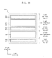
- FIG. 11 is a plan view illustrating an organic light emitting display device according to an exemplary embodiment.
- An organic light emitting display device 400 illustrated in FIG. 11 may have a configuration substantially similar to organic light emitting display device 100 described with reference to FIG. 1 .
- FIG. 11 detailed descriptions for elements that are substantially similar to the elements described with reference to FIG. 1 will be omitted for brevity.
- an organic light emitting display (OLED) device 400 may include a pixel region I and a transparent region II.
- the pixel region I may be a non-uniform by having separate sub-pixel regions.
- the transparent region II may be non-uniform by having separate sub-transparent regions.
- the sub-pixel regions of pixel region I may be separated from one another by sub-transparent regions of the transparent region II and vice versa.
- the pixel region I may include a first sub-pixel region V, a second sub-pixel region VI, and a third sub-pixel region VII.
- the transparent region II may include a first sub-transparent region VIII and a second sub-transparent region IX.
- a first sub-pixel 415, a second sub-pixel 420, and a third sub-pixel 425 may be located in the first, second, and third sub-pixel regions V, VI, and VII, respectively.
- the first transparent window 470 and the second transparent 475 may be located in the first and second sub-transparent regions VIII and IX, respectively.
- the first sub-pixel 415 may be a pixel emitting a red color and may extend along a first direction.
- the second sub-pixel 420 may be a pixel emitting a green color and may be disposed substantially parallel to the first sub-pixel 415.
- the third sub-pixel 425 may be a pixel emitting a blue color and may be disposed substantially parallel to the first sub-pixel 415 and the second sub-pixel 420.
- the first, second, and third sub-pixels 415, 420, and 425 may be located at the same level on a substrate.
- the first, second, and third sub-pixels 415, 420, and 425 may extend along the first direction because the first, second, and third sub-pixels 415, 420, and 425 are manufactured through an SMS method.
- the first and second transparent windows 470 and 475 may transmit an external light in the transparent region II (i.e., first sub-transparent region VIII and second sub-transparent region IX, respectively).
- common lines and insulating layers may be disposed in a portion that surrounds the first, second, and third sub-pixels 415, 420, and 425 and the first and second transparent windows 470 and 475.
- a pixel defining layer 410 may surround the first, second, and third sub-pixels 415, 420, and 425 and the first and second transparent windows 470 and 475.
- the OLED device 400 may include a plurality of upper electrodes 430, 435, and 440.
- the upper electrode 430 may be disposed on the first sub-pixel 415 in the first sub-pixel region V and may extend along the first direction.
- the upper electrode 435 may be disposed on the second sub-pixel 420 in the second sub-pixel region VI and may extend along the first direction.
- the upper electrode 440 may be disposed on the third sub-pixel 425 in the third sub-pixel region VII and may extend along the first direction.
- the upper electrodes 430, 435, and 440 are not located in the first and second sub-transparent regions VIII and IX.
- the upper electrodes 430, 435, and 440 may expose the first and second sub-transparent regions VIII and IX.
- the first sub-transparent region VIII may be located between the first sub-pixel region V and the second sub-pixel region VI.
- the first transparent window 470 may be interposed between the first sub-pixel 415 and the second sub-pixel 420.
- the second sub-transparent region IX may be located between the second sub-pixel region VI and the third sub-pixel region VII.
- the second transparent window 475 may be interposed between the second sub-pixel 420 and the third sub-pixel 425.
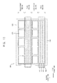
- FIG. 12 is a plan view illustrating an organic light emitting display device according to an exemplary embodiment.
- An organic light emitting display device 500 illustrated in FIG. 12 may have a configuration substantially similar to organic light emitting display device 400 described with reference to FIG. 11 except for an auxiliary electrode 510.
- FIG. 12 detailed descriptions for elements that are substantially similar to the elements described with reference to FIG. 11 will be omitted for brevity.
- an organic light emitting display (OLED) device 500 may include a pixel region I and a transparent region II.
- the pixel region I may be non-uniform by having separate sub-pixel regions.
- the transparent region II may be non-uniform by having separate sub-transparent regions.
- the sub-pixel regions of pixel region I may be separated from one another by sub-transparent regions of the transparent region II and vice versa.
- the pixel region I may include a first sub-pixel region V, a second sub-pixel region VI, and a third sub-pixel region VII.
- the transparent region II may include a first sub-transparent region VIII and a second sub-transparent region IX.
- a first sub-pixel 415, a second sub-pixel 420, and a third sub-pixel 425 may be located in the first, second, and third sub-pixel regions V, VI, and VII, respectively.
- a first transparent window 470 and a second transparent window 475 may be located in the first and second sub-transparent regions VIII and IX, respectively.
- the first sub-pixel 415 may be a pixel emitting a red color and may extend along a first direction.
- the second sub-pixel 420 may be a pixel emitting a green color and may be disposed substantially parallel to the first sub-pixel 415.
- the third sub-pixel 425 may be a pixel emitting a blue color and may be disposed in substantially parallel to the first sub-pixel 415 and the second sub-pixel 420.
- the first, second, and third sub-pixels 415, 420, and 425 may be located at the same level on a substrate.
- the first, second, and third sub-pixels 415, 420, and 425 may extend along the first direction because the first, second, and third sub-pixels 415, 420, and 425 are manufactured through an SMS method.
- the first and second transparent windows 470 and 475 may transmit an external light in the transparent region II.
- common lines and insulating layers may be disposed in a portion that surrounds the first, second, and third sub-pixels 415, 420, and 425 and the first and second transparent windows 470 and 475.
- a pixel defining layer 410 may surround the first, second, and third sub-pixels 415, 420, and 425 and the first and second transparent windows 470 and 475.
- the OLED device 400 may include a plurality of upper electrodes 430, 435, and 440.
- the upper electrode 430 may be disposed on the first sub-pixel 415 in the first sub-pixel region V and may extend along the first direction.
- the upper electrode 435 may be disposed on the second sub-pixel 420 in the second sub-pixel region VI and may extend along the first direction.
- the upper electrode 440 may be disposed on the third sub-pixel 425 in the third sub-pixel region VII and may extend along the first direction.
- the upper electrodes 430, 435, and 440 are not located in the first and second sub-transparent regions VIII and IX.
- the upper electrodes 430, 435, and 440 may expose the first and second sub-transparent regions VIII and IX.
- the first sub-transparent region VIII may be located between the first sub-pixel region V and the second sub-pixel region VI.
- the first transparent window 470 may be interposed between the first sub-pixel 415 and the second sub-pixel 420.
- the second sub-transparent region IX may be located between the second sub-pixel region VI and the third sub-pixel region VII.
- the second transparent window 475 may be interposed between the second sub-pixel 420 and the third sub-pixel 425.
- an auxiliary electrode 510 may be interposed between the upper electrodes 430, 435, and 440 and the first, second, and third sub-pixels 415, 420, and 425.
- the auxiliary electrode 510 may extend along the first direction and the second direction.
- the auxiliary electrode 510 may be located in the transparent region II as well as the pixel region I.
- the auxiliary electrode 510 may be disposed in the same chamber as the first, second, and third sub-pixels 415, 420, and 425 but are disposed after the first, second, and third sub-pixels 415, 420, and 425. Then, the upper electrodes 430, 435, and 440 may be disposed through the FMM method. In an alternate embodiment, the auxiliary electrode 510 may be disposed on the upper electrodes 430, 435, and 440.
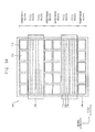
- FIG. 13 is a plan view illustrating an organic light emitting display device according to an exemplary embodiment.
- An organic light emitting display device 600 illustrated in FIG. 13 may have a configuration substantially similar to organic light emitting display device 300 described with reference to FIG. 4 .
- FIG. 13 detailed descriptions for elements that are substantially similar to the elements described with reference to FIG. 4 will be omitted for brevity.
- an organic light emitting display (OLED) device 600 may include a plurality of pixel regions I and a plurality of transparent regions II.
- a first sub-pixel 615, a second sub-pixel 620, and a third sub-pixel 625 may be located in the plurality of pixel regions I.
- Transparent windows 670 may be located in the plurality of transparent regions II.
- the pixel regions I and the transparent regions II may be repeatedly arranged in a first direction and alternately arranged in a second direction.
- one pixel region I or one transparent region II may be repeatedly arranged in a first direction.
- the repeatedly arranged pixel regions I and the repeatedly arranged transparent regions II may be alternately arranged in the second direction that is substantially perpendicular to the first direction.
- an auxiliary electrode 640 may be entirely located on the substrate in the pixel regions I and the transparent regions II.
- the first sub-pixel 615 may be a pixel emitting a red color and may extend along a first direction.
- the second sub-pixel 620 may be a pixel emitting a green color and may be disposed in substantially parallel to the first sub-pixel 615.
- the third sub-pixel 625 may be a pixel emitting a blue color and may be disposed in substantially parallel to the first sub-pixel 615 and the second sub-pixel 620.
- the first, second, and third sub-pixels 615, 620, and 625 may be located at the same level on a substrate.
- the first, second, and third sub-pixels 615, 620, and 625 may extend along the first direction because the first, second, and third sub-pixels 615, 620, and 625 are manufactured through an SMS method.
- the transparent windows 670 may transmit an external light.
- common lines and insulating layers may be disposed in a portion that surrounds the first, second, and third sub-pixels 615, 620, and 625 and the transparent windows 670.
- a pixel defining layer 610 may surround the first, second, and third sub-pixels 615, 620, and 625 and the transparent windows 670.
- an upper electrode 630 may be disposed on the first, second, and third sub-pixels 615, 620, and 625 in the pixel region I and may extend along the first direction.
- the upper electrode 630 is not located in the transparent region II.
- the upper electrode 630 may expose the transparent regions II.
- the auxiliary electrode 640 may be interposed between the upper electrode 630 and the first, second, and third sub-pixels 615, 620, and 625 and may be entirely disposed on the pixel defining layer 610.
- the auxiliary electrode 640 may be located in the transparent region II as well as the pixel region I.
- the auxiliary electrode 640 may be disposed in the same chamber as the first, second, and third sub-pixels 615, 620, and 625 but after the first, second, and third sub-pixels 615, 620, and 625..
- an upper electrode 630 may be disposed through an FMM method.
- FIG. 14 is a plan view illustrating an organic light emitting display device according to an exemplary embodiment.
- An organic light emitting display device 700 illustrated in FIG. 14 may have a configuration substantially similar to organic light emitting display device 300 described with reference to FIG. 4 .
- FIG. 14 detailed descriptions for elements that are substantially similar to elements described with reference to FIG. 4 will be omitted for brevity.
- an organic light emitting display (OLED) device 700 may include a plurality of pixel regions I and a plurality of transparent regions II.
- a first sub-pixel 715, a second sub-pixel 720, and a third sub-pixel 725 may be located in the pixel regions I.
- Transparent windows 770 may be located in the transparent regions II.
- At least two pixel regions I and at least two transparent regions II may be repeatedly arranged in a first direction and alternately arranged in a second direction. For example, the at least two adjacent pixel regions I in the second direction and the at least two adjacent transparent regions II in the second direction may be repeatedly arranged in a first direction.
- the repeatedly arranged pixel regions I in the first direction and the repeatedly arranged transparent regions II in the first direction may be alternately arranged in the second direction in pairs.
- two pixel regions I are adjacent to each other in the second direction forming a pixel region I pair and two transparent regions II are also adjacent to each other in the second direction forming a transparent region II pair.
- the pixel region I pair is alternately arranged with the transparent region II pair in the second direction.
- the first direction is substantially perpendicular to the second direction.
- an auxiliary electrode 740 may be entirely located on the substrate in the pixel regions I and the transparent regions II of the OLED device 700.
- the first sub-pixel 715 may be a pixel emitting a red color and may extend along a first direction.
- the second sub-pixel 720 may be a pixel emitting a green color and may be disposed substantially parallel to the first sub-pixel 715.
- the third sub-pixel 725 may be a pixel emitting a blue color and may be disposed substantially parallel to the first sub-pixel 715 and the second sub-pixel 720.
- the first, second, and third sub-pixels 715, 720, and 725 may be located at the same level on a substrate.
- the first, second, and third sub-pixels 715, 720, and 725 may extend along the first direction because the first, second, and third sub-pixels 715, 720, and 725 are manufactured through an SMS method.
- the transparent windows 770 may transmit an external light.
- common lines and insulating layers may be disposed in a portion that surrounds the first, second, and third sub-pixels 715, 720, and 725 and the transparent windows 770.
- a pixel defining layer 710 may surround the first, second, and third sub-pixels 715, 720, and 725 and the transparent windows 770.
- an upper electrode 730 may be disposed on the first, second, and third sub-pixels 715, 720, and 725 in the pixel region I and may extend along the first direction.
- the upper electrode 730 may extend across two adjacent pixel regions I.
- the upper electrode 730 is not located in a transparent region II.
- the upper electrode 730 may expose a transparent region II.
- the auxiliary electrode 740 may be interposed between the upper electrode 730 and the first, second, and third sub-pixels 715, 720, and 725 and may be entirely disposed on the pixel defining layer 710.
- the auxiliary electrode 740 may be located in the pixel regions I and transparent regions II.
- the auxiliary electrode 740 may be disposed in the same chamber as the first, second, and third sub-pixels 715, 720, and 725 but after the first, second, and third sub-pixels 715, 720, and 725. Then, an upper electrode 730 may be disposed through an FMM method.
- An organic light emitting display device includes a relatively thick upper electrode in a pixel region resulting in an increased definition of an image of an object transmitted through a transparent region.
- the organic light emitting display device may have a reduced IR drop phenomenon compared to organic light emitting display devices without an auxiliary electrode.
- embodiments of the invention can provide an organic light emitting display device, comprising: a substrate extending along a first direction, the substrate comprising a pixel region having a plurality of pixels and a transparent region that is located adjacent to the pixel region; a lower electrode disposed over the substrate in the pixel region, the lower electrode extending along the first direction; a light emitting layer disposed over the lower electrode, the light emitting layer extending along the first direction; and an upper electrode disposed over the light emitting layer in the pixel region, the upper electrode extending along the first direction, wherein the upper electrode is arranged to expose the transparent region.
- the upper electrode is located in the pixel region and not in the transparent region.
- the upper electrode may be relatively thick and may have a thickness of greater than or equal to 10 nm.
- auxiliary electrode disposed over the upper electrode.
- the auxiliary electrode may be relatively thin and may have a thickness of less than or equal to 7.5 nm.
- the auxiliary electrode extends from the pixel region into the transparent region along a second direction that is substantially perpendicular to the first direction. Hence, in such embodiments, the auxiliary electrode is located in the pixel region and in the transparent region.
- the auxiliary electrode is disposed in the pixel region and the auxiliary electrode exposes the transparent region.
- the auxiliary electrode is located in the pixel region and not in the transparent region.
- the pixel region comprises a number of sub-pixel regions. In some embodiments, these sub-pixel regions can be arranged adjacent to each other, with the transparent region adjacent sub-pixel regions. In such embodiments, the upper electrode may be shared for the sub-pixel regions.
- the sub-pixel regions can be arranged with sub-transparent regions therebetween.
- the upper electrode may be located above the sub-pixel regions.
- the present invention may be applied to various display devices including an organic light emitting display device.
- the present invention may be applied to vehicle-display device, a ship-display device, an aircraft-display device, portable communication devices, display devices for display or for information transfer, a medical-display device, etc.
Landscapes
- Physics & Mathematics (AREA)
- Optics & Photonics (AREA)
- Engineering & Computer Science (AREA)
- Microelectronics & Electronic Packaging (AREA)
- Geometry (AREA)
- Electroluminescent Light Sources (AREA)
Abstract
Description
- Exemplary embodiments relate generally to organic light emitting display devices. More particularly, exemplary relate to organic light emitting display devices including a pixel region and a transparent region.
- A flat panel display (FPD) device is widely used as a display device of an electronic device because the FPD device is lightweight and thin compared to cathode-ray tube (CRT) display devices. Typical examples of the FPD device are a liquid crystal display (LCD) device and an organic light emitting display (OLED) device. Compared to the LCD device, the OLED device has many advantages such as a higher luminance and a wider viewing angle. In addition, the OLED device can be made thinner because the OLED device does not require a backlight. In the OLED device, electrons and holes are injected into an organic thin layer through a cathode and an anode, and then recombined in the organic thin layer to generate excitons, thereby a light of a certain wavelength can be emitted.
- Recently, a transparent OLED device has been developed that is capable of transmitting an image of an object (or target) that is located in the rear (or at the back) of the OLED device by including a transparent region and a pixel region. In this case, a transmissivity of a light incident into the transparent region may be decreased by a cathode electrode located in the transparent region. In addition, an IR drop (i.e., voltage drop) may be generated because the cathode electrode is made relatively thin. Thus, a definition (e.g., visibility) of the image of the object that is located in the rear of a conventional OLED device may be reduced due to the decrease of the transmissivity, and a uniform luminance is not provided in the conventional OLED device because of the IR drop.
- The above information disclosed in this Background section is only for enhancement of understanding of the background of the inventive concept, and, therefore, it may contain information that does not form the prior art that is already known in this country to a person of ordinary skill in the art.
- Exemplary embodiments provide an organic light emitting display device including a relatively thick upper electrode in a pixel region.
- Additional aspects will be set forth in the detailed description which follows, and, in part, will be apparent from the disclosure, or may be learned by practice of the inventive concept.
- An exemplary embodiment discloses an organic light emitting display device that includes a substrate extending along a first direction, the substrate comprising a pixel region having a plurality of pixels and a transparent region that is located adjacent to the pixel region, a lower electrode disposed on the substrate in the pixel region, the lower electrode extending along the first direction, a light emitting layer disposed on the lower electrode, the light emitting layer extending along the first direction, and an upper electrode disposed on the light emitting layer in the pixel region, the upper electrode extending along the first direction. The upper electrode exposes the transparent region.
- According to an aspect of the invention, there is provided an organic light emitting display device as set out in claim 1. Preferred features are set out in
claims 2 to 15. - The foregoing general description and the following detailed description are exemplary and explanatory and are intended to provide further explanation of the claimed subject matter.
- The accompanying drawings, which are included to provide a further understanding of the inventive concept, and are incorporated in and constitute a part of this specification, illustrate exemplary embodiments of the inventive concept, and, together with the description, serve to explain principles of the inventive concept.
-
FIG. 1 is a plan view illustrating an organic light emitting display device according to an exemplary embodiment. -
FIG. 2 is a cross sectional view illustrating an organic light emitting display device taken along line III-III' ofFIG. 1 . -
FIG. 3 is a cross sectional view illustrating an organic light emitting display device according to an exemplary embodiment. -
FIG. 4 is a plan view illustrating an organic light emitting display device according to an exemplary embodiment. -
FIG. 5 is a cross sectional view illustrating an organic light emitting display device taken along line IV-IV' ofFIG. 4 . -
FIG. 6 is a cross sectional view illustrating an organic light emitting display device according to an exemplary embodiment. -
FIG. 7 is a cross sectional view illustrating an organic light emitting display device according to an exemplary embodiment. -
FIG. 8 is a cross sectional view illustrating an organic light emitting display device according to an exemplary embodiment. -
FIG. 9 is a plan view illustrating an organic light emitting display device according to an exemplary embodiment. -
FIGS. 10A ,10B ,10C ,10D ,10E , and10F are cross sectional views illustrating a method of manufacturing an organic light emitting display device according to an exemplary embodiment. -
FIG. 11 is a plan view illustrating an organic light emitting display device in according to an exemplary embodiment. -
FIG. 12 is a plan view illustrating an organic light emitting display device according to an exemplary embodiment. -
FIG. 13 is a plan view illustrating an organic light emitting display device according to an exemplary embodiment. -
FIG. 14 is a plan view illustrating an organic light emitting display device according to an embodiment. - In the following description, for the purposes of explanation, numerous specific details are set forth in order to provide a thorough understanding of various exemplary embodiments. It is apparent, however, that various exemplary embodiments may be practiced without these specific details or with one or more equivalent arrangements. In other instances, well-known structures and devices are shown in block diagram form in order to avoid unnecessarily obscuring various exemplary embodiments.
- In the accompanying figures, the size and relative sizes of layers, films, panels, regions, etc., may be exaggerated for clarity and descriptive purposes. Also, like reference numerals denote like elements.
- When an element or layer is referred to as being "on," "connected to," or "coupled to" another element or layer, it may be directly on, connected to, or coupled to the other element or layer or intervening elements or layers may be present. When, however, an element or layer is referred to as being "directly on," "directly connected to," or "directly coupled to" another element or layer, there are no intervening elements or layers present. For the purposes of this disclosure, "at least one of X, Y, and Z" and "at least one selected from the group consisting of X, Y, and Z" may be construed as X only, Y only, Z only, or any combination of two or more of X, Y, and Z, such as, for instance, XYZ, XYY, YZ, and ZZ. Like numbers refer to like elements throughout. As used herein, the term "and/or" includes any and all combinations of one or more of the associated listed items.
- Although the terms first, second, etc. may be used herein to describe various elements, components, regions, layers, and/or sections, these elements, components, regions, layers, and/or sections should not be limited by these terms. These terms are used to distinguish one element, component, region, layer, and/or section from another element, component, region, layer, and/or section. Thus, a first element, component, region, layer, and/or section discussed below could be termed a second element, component, region, layer, and/or section without departing from the teachings of the present disclosure.
- Spatially relative terms, such as "beneath," "below," "lower," "above," "upper," and the like, may be used herein for descriptive purposes, and, thereby, to describe one element or feature's relationship to another element(s) or feature(s) as illustrated in the drawings. Spatially relative terms are intended to encompass different orientations of an apparatus in use, operation, and/or manufacture in addition to the orientation depicted in the drawings. For example, if the apparatus in the drawings is turned over, elements described as "below" or "beneath" other elements or features would then be oriented "above" the other elements or features. Thus, the exemplary term "below" can encompass both an orientation of above and below. Furthermore, the apparatus may be otherwise oriented (e.g., rotated 90 degrees or at other orientations), and, as such, the spatially relative descriptors used herein interpreted accordingly.
- The terminology used herein is for the purpose of describing particular embodiments and is not intended to be limiting. As used herein, the singular forms, "a," "an," and "the" are intended to include the plural forms as well, unless the context clearly indicates otherwise. Moreover, the terms "comprises," "comprising," "includes," and/or "including," when used in this specification, specify the presence of stated features, integers, steps, operations, elements, components, and/or groups thereof, but do not preclude the presence or addition of one or more other features, integers, steps, operations, elements, components, and/or groups thereof.
- Various exemplary embodiments are described herein with reference to sectional illustrations that are schematic illustrations of idealized exemplary embodiments and/or intermediate structures. As such, variations from the shapes of the illustrations as a result, for example, of manufacturing techniques and/or tolerances, are to be expected. Thus, exemplary embodiments disclosed herein should not be construed as limited to the particular illustrated shapes of regions, but are to include deviations in shapes that result from, for instance, manufacturing. For example, an implanted region illustrated as a rectangle will, typically, have rounded or curved features and/or a gradient of implant concentration at its edges rather than a binary change from implanted to non-implanted region. Likewise, a buried region formed by implantation may result in some implantation in the region between the buried region and the surface through which the implantation takes place. Thus, the regions illustrated in the drawings are schematic in nature and their shapes are not intended to illustrate the actual shape of a region of a device and are not intended to be limiting.
- Unless otherwise defined, all terms (including technical and scientific terms) used herein have the same meaning as commonly understood by one of ordinary skill in the art to which this disclosure is a part. Terms, such as those defined in commonly used dictionaries, should be interpreted as having a meaning that is consistent with their meaning in the context of the relevant art and will not be interpreted in an idealized or overly formal sense, unless expressly so defined herein.
- Hereinafter, exemplary embodiments will be explained in detail with reference to the accompanying drawings.
-
FIG. 1 is a plan view illustrating an organic light emitting display device according to an exemplary embodiment. - Referring to
FIG. 1 , an organic light emitting display (OLED)device 100 may include a pixel region I and a transparent region II. Afirst sub-pixel 315, asecond sub-pixel 320, and athird sub-pixel 325 may be located in the pixel region I, and atransparent window 370 may be located in the transparent region II. - In the pixel region I, the
first sub-pixel 315 may be a pixel emitting a red color and may extend along a first direction. Thesecond sub-pixel 320 may be a pixel emitting a green color and may be disposed substantially parallel to thefirst sub-pixel 315. Thethird sub-pixel 325 may be a pixel emitting a blue color and may be disposed substantially parallel to thefirst sub-pixel 315 and thesecond sub-pixel 320. The first, second, and third sub-pixels 315, 320, and 325 may be located at the same level on a substrate. For example, the first, second, and third sub-pixels 315, 320, and 325 may extend along the first direction because the first, second, and third sub-pixels 315, 320, and 325 are manufactured through a Small Mask Scanning (SMS) method. - In the transparent region II, the
transparent window 370 may transmit an external light. Here, common lines (i.e., data lines, scan lines, power supply lines, etc.) and insulating layers (i.e., a pixel defining layer, a protection layer, etc.) may be disposed in a portion (e.g., a dead space) that surrounds the first, second, and third sub-pixels 315, 320, and 325 and thetransparent window 370. For example, apixel defining layer 310 may surround the first, second, and third sub-pixels 315, 320, and 325 and thetransparent window 370. - In an exemplary embodiment, an
upper electrode 330 of theOLED device 100 may be disposed on the first, second, and third sub-pixels 315, 320, and 325 in the pixel region I. Theupper electrode 330 may extend along the first direction. In this case, theupper electrode 330 is not located in the transparent region II. Thus, theupper electrode 330 may expose the transparent region II. -
FIG. 2 is a cross sectional view illustrating an organic light emitting display device taken along line III-III' ofFIG. 1 . - Referring to
FIG. 2 , an organic light emitting display (OLED)device 100 may include asubstrate 110, a first insulatinglayer 150, a second insulatinglayer 190, a thirdinsulating layer 270, a drivingtransistor 250, alower electrode 290, apixel defining layer 310, a light emitting layer of first sub-pixel 315 (equally applicable to the light emitting layers of theother sub-pixels 320 and 325), anupper electrode 330, atransparent window 370, and anencapsulation substrate 350. Here, the drivingtransistor 250 may include anactive layer 130, agate electrode 170, asource electrode 210, and adrain electrode 230. - As described above, the
OLED device 100 may include a pixel region I and a transparent region II. The drivingtransistor 250, thelower electrode 290, the light emitting layer offirst sub-pixel 315, and theupper electrode 330 may be located in the pixel region I. In addition, thetransparent window 370 may be located in the transparent region II. For example, a display image may be displayed in the pixel region I. An image of an object that is located in the rear of theOLED device 100 may be transmitted in the transparent region II. Because theOLED device 100 has the transparent region II, theOLED device 100 may serve as a transparent display device. - The
substrate 110 may include transparent materials. For example, thesubstrate 110 may include quartz, synthetic quartz, calcium fluoride, fluoride-doping quartz, a soda lime glass, and a non-alkali glass. Thesubstrate 110 may include any other suitable material. In an alternative embodiment, thesubstrate 110 may include a flexible transparent resin substrate. Here, the flexible transparent resin substrate for thesubstrate 110 may include a polyimide substrate. For example, the polyimide substrate may include a first polyimide layer, a barrier film layer, and a second polyimide layer. When the polyimide substrate is thin and flexible, the polyimide substrate may be formed on a rigid glass substrate to help support the formation of an upper structure (e.g., the drivingtransistor 250, thelower electrode 290, the light emitting layer offirst sub-pixel 315, and the upper electrode 330). Thus, in an exemplary embodiment, thesubstrate 110 may have a structure that includes the first polyimide layer, the barrier film layer, and the second polyimide layer stacked on a glass substrate. Here, after an insulation layer is disposed on the second polyimide layer, the upper structure may be disposed on the insulation layer. After the upper structure is formed on the insulation layer, the glass substrate may be removed. It may be difficult to directly form the upper structure on the polyimide substrate because the polyimide substrate is thin and flexible. Accordingly, the upper structure is formed on a rigid glass substrate, and then the polyimide substrate may serve as thesubstrate 110 after the removal of the glass substrate. Because theOLED device 100 includes the pixel region I and the transparent region II, thesubstrate 110 may also include the pixel region I and the transparent region II. - Referring to again
FIG. 2 , the buffer layer (not shown) may be disposed on thesubstrate 110. The buffer layer may extend from the pixel region I into the transparent region II. The buffer layer may prevent the diffusion of metal atoms and/or impurities from thesubstrate 110. Additionally, the buffer layer may control a rate of heat transfer in a crystallization process for forming anactive layer 130, thereby obtaining a substantially uniformactive layer 130. Furthermore, the buffer layer may improve surface flatness of thesubstrate 110 when a surface of thesubstrate 110 is relatively irregular. For example, the buffer layer may include at least one of silicon nitride and silicon oxide. The buffer layer may include any other suitable material. In an exemplary embodiment, according to a type of thesubstrate 110, at least two buffer layers may be provided on thesubstrate 110. In another exemplary embodiment the buffer layer is not disposed on thesubstrate 110. - The driving
transistor 250 may include theactive layer 130, thegate electrode 170, thesource electrode 210, and thedrain electrode 230. In an exemplary embodiment, theactive layer 130 may be disposed on thesubstrate 110. Theactive layer 130 may include at least one of an oxide semiconductor, an inorganic semiconductor (i.e., amorphous silicon, polysilicon, etc.), and an organic semiconductor. Theactive layer 130 may include any other suitable material. - The first insulating
layer 150 may be disposed on theactive layer 130. The first insulatinglayer 150 may cover theactive layer 130 in the pixel region I, and may extend into the transparent region II. Thus, the first insulatinglayer 150 may be entirely disposed in the pixel region I and the transparent region II of thesubstrate 110. The first insulatinglayer 150 may include at least one of a silicon compound and a metal oxide. The first insulatinglayer 150 may include any other suitable material. - The
gate electrode 170 may be disposed on the first insulatinglayer 150 directly over theactive layer 130, which is located under the first insulatinglayer 150. Thegate electrode 170 may include at least one of metal, metal alloy, metal nitride, conductive metal oxide, and transparent conductive materials. Thegate electrode 170 may include any other suitable material. - The second
insulating layer 190 may be disposed on thegate electrode 170. The secondinsulating layer 190 may cover thegate electrode 170 in the pixel region I and may extend into the transparent region II. Thus, the second insulatinglayer 190 may be entirely disposed in the pixel region I and the transparent region II of thesubstrate 110. The secondinsulating layer 190 may include at least one of a silicon compound and a metal oxide. The secondinsulating layer 190 may include any other suitable material. - The
source electrode 210 and thedrain electrode 230 may be disposed on the second insulatinglayer 190. Thesource electrode 210 may contact a first side of theactive layer 130 by removing a portion of the first and second insulatinglayer drain electrode 230 may contact a second side of theactive layer 130 by removing a second portion of the first and second insulatinglayer source electrode 210 and thedrain electrode 230 may include at least one of metal, metal alloy, metal nitride, conductive metal oxide, and transparent conductive materials. Thesource electrode 210 and thedrain electrode 230 may include any other suitable material. - The third
insulating layer 270 may be disposed on thesource electrode 210 and thedrain electrode 230. The thirdinsulating layer 270 may cover thesource electrode 210 and thedrain electrode 230 in the pixel region I, and may extend into the transparent region II. Thus, the third insulatinglayer 270 may be entirely disposed in the pixel region I and the transparent region II of thesubstrate 110. The thirdinsulating layer 270 may include at least one of a silicon compound and a metal oxide. The thirdinsulating layer 270 may include any other suitable material. - As illustrated in
FIG. 2 , thelower electrode 290 may be disposed on the third insulatinglayer 270. Thelower electrode 290 may contact thesource electrode 210 by removing a portion of the third insulatinglayer 270. Thelower electrode 290 may include at least one of metal, metal alloy, metal nitride, conductive metal oxide, and transparent conductive materials. - The
pixel defining layer 310 may be disposed the on third insulatinglayer 270 to expose a portion of thelower electrode 290. Thepixel defining layer 310 may include at least one of organic materials and inorganic materials. In this case, thepixel defining layer 310 may include a first opening and a second opening. In the pixel region I, the first opening of thepixel defining layer 310 may expose a portion of thelower electrode 290. The light emitting layer offirst sub-pixel 315 may be disposed on the exposedlower electrode 290. In addition, in the transparent region II, the second opening of thepixel defining layer 310 may expose a portion of the third insulatinglayer 270. The second opening may be thetransparent window 370. In an alternate embodiment, the second opening is not disposed on the third insulatinglayer 270, and the transparent region II may be thetransparent window 370. Thus, thepixel defining layer 310 may have a plan upper surface in the transparent region II. - The light emitting layer of
first sub-pixel 315 may be disposed on the exposedlower electrode 290. The light emitting layer offirst sub-pixel 315 may be formed using light emitting materials capable of generating different colors of light (e.g., a red color of light, a blue color of light, and a green color of light) according to the first, second, and third sub-pixels 315, 320, and 325 illustrated inFIG. 1 . For example, the light emitting layer offirst sub-pixel 315 illustrated inFIG. 2 may be formed using the light emitting material capable of generating the red color of light. - The
upper electrode 330 may be disposed on thepixel defining layer 310 and the light emitting layer offirst sub-pixel 315 in the pixel region I. Theupper electrode 330 is not located in the transparent region II. Thus, theupper electrode 330 may expose the transparent region II. Theupper electrode 330 may be shared by the first, second, and third sub-pixels 315, 320, and 325 (shown inFIG. 1 ). In an exemplary embodiment, theupper electrode 330 may be relatively thick. For example, a thickness of theupper electrode 330 may be over about 10 nm (100 Å, angstrom). In this case, a light transmissivity of theupper electrode 330 may be below about 50%. Theupper electrode 330 may include at least one of metal, metal alloy, metal nitride, conductive metal oxide, and a transparent conductive material. For example, theupper electrode 330 may include at least one of aluminum (Al), aluminum alloy, aluminum nitride (AlNx), silver (Ag), silver alloy, tungsten (W), tungsten nitride (WNx), copper (Cu), copper alloy, nickel (Ni), chrome (Cr), chrome nitride (CrNx), molybdenum (Mo), molybdenum alloy, magnesium (Mg), magnesium alloy, magnesium-silver (Mg-Ag) alloy, titanium (Ti), titanium nitride (TiNx), platinum (Pt), tantalum (Ta), tantalum nitride (TaNx), neodymium (Nd), scandium (Sc), strontium ruthenium oxide (SRO), zinc oxide (ZnOx), aluminum zinc oxide (AZO), indium tin oxide (ITO), stannum oxide (SnOx), indium oxide (InOx), indium tin oxide (ITO), gallium oxide (GaOx), gallium zinc oxide (GZO), and indium zinc oxide (IZO). Theupper electrode 330 may use any other suitable material as well. In an exemplary embodiment, theupper electrode 330 may include magnesium-silver (Mg-Ag) alloy. Compared to a conventional OLED device, theOLED device 100 includes the relatively thickupper electrode 330, resulting in a reduced generation of IR drop (i.e., voltage drop) in theOLED device 100. Accordingly, a uniform luminance may be provided in theOLED device 100. In addition, because theupper electrode 330 is not located in the transparent region II, the transmissivity of theOLED device 100 may be increased. A definition (e.g., visibility) of an image of an object that is located in the rear (e.g., at the back) of theOLED device 100 may be increased. - The
encapsulation substrate 350 may be disposed on theupper electrode 330,pixel defining layer 310, and thetransparent window 370. Theencapsulation substrate 350 and thesubstrate 110 may include substantially the same materials. For example, theencapsulation substrate 350 may include at least one of quartz, synthetic quartz, calcium fluoride, fluoride-doping quartz, soda lime glass, and non-alkali glass. Theencapsulation substrate 350 may include any other suitable material. In an exemplary embodiment, theencapsulation substrate 350 may include at least one of a transparent inorganic material and a flexible plastic. For example, theencapsulation substrate 350 may include a flexible transparent resin substrate. In this case, to increase flexibility of theOLED device 100, theencapsulation substrate 350 may include a stacked structure where at least one organic layer and at least one inorganic layer are alternately stacked. In an alternate embodiment, when the first insulatinglayer 150, the second insulatinglayer 190, and the third insulatinglayer 270 have the same materials, and thesubstrate 110, theencapsulation substrate 350, the first insulatinglayer 150, the second insulatinglayer 190, and the third insulatinglayer 270 have a same (or similar) refractive index, a light incident into the transparent region II is not refracted by the interfaces of thesubstrate 110, theencapsulation substrate 350, the first insulatinglayer 150, the second insulatinglayer 190, and the third insulatinglayer 270. Accordingly, the transmissivity of theOLED device 100 may be increased, and the definition of the image may be improved. - The
OLED device 100 according to exemplary embodiments includes the relatively thickupper electrode 330, which may only be located in the pixel region I. Accordingly, theOLED device 100 may serve as a transparent display device with improved transmissivity. In addition, because theupper electrode 330 is not located in the transparent region II, theOLED device 100 may have increased transmissivity. TheOLED device 100 may have an increased definition of the image of the object that is located in the rear of theOLED device 100. Further, when the first insulatinglayer 150, the second insulatinglayer 190, and the third insulatinglayer 270 include the same materials, theOLED device 100 may have a decrease in contact interfaces capable of reflecting a light. Thus, the resultingOLED 100 may have an increased transmissivity and definition of the image of the object that is located in the rear of theOLED device 100. -
FIG. 3 is a cross sectional view illustrating an organic light emitting display device according to an exemplary embodiment. An organic light emitting display device illustrated inFIG. 3 may have a configuration substantially similar the organic light emittingdisplay device 100 described with reference toFIG. 2 except for a shape oftransparent window 375. InFIG. 3 , detailed descriptions for elements that are substantially similar to the elements described with reference toFIG. 2 will be omitted for brevity. - Referring to
FIG. 3 , an organic light emitting display (OLED) device may include at least one of asubstrate 110, a first insulatinglayer 150, a second insulatinglayer 190, a thirdinsulating layer 270, a drivingtransistor 250, alower electrode 290, apixel defining layer 310, a light emitting layer offirst sub-pixel 315, anupper electrode 330, atransparent window 375, and anencapsulation substrate 350. Here, the drivingtransistor 250 may include anactive layer 130, agate electrode 170, asource electrode 210, and adrain electrode 230. In an exemplary embodiment, the OLED device may include a pixel region I and a transparent region II. The drivingtransistor 250, thelower electrode 290, the light emitting layer offirst sub-pixel 315, and theupper electrode 330 may be located in the pixel region I. In addition, thetransparent window 375 may be located in the transparent region II. For example, a display image may be displayed in the pixel region I. An image of an object that is located in the rear of the OLED device may be transmitted in the transparent region II. Accordingly, the OLED device having the transparent region II may serve as a transparent display device. - The
pixel defining layer 310 may be disposed on the third insulatinglayer 270 to expose a portion of thelower electrode 290. Thepixel defining layer 310 may include at least one of organic materials and inorganic materials. In this case, thepixel defining layer 310 may include a first opening and a second opening. In the pixel region I, the first opening of thepixel defining layer 310 may expose a portion of thelower electrode 290. The light emitting layer offirst sub-pixel 315 may be disposed on the exposedlower electrode 290. In addition, in the transparent region II, the second opening of thepixel defining layer 310 may expose a portion of the third insulatinglayer 270. The second opening of thepixel defining layer 310 may extend through the third insulatinglayer 270, the second insulating 190, and the first insulating layer. The second opening may be thetransparent window 375. In an exemplary embodiment, thetransparent window 375 may be formed by removing a portion of the first insulatinglayer 150, a portion of the second insulatinglayer 190, a portion of the third insulatinglayer 270, and a portion of thepixel defining layer 310. In an exemplary embodiment, portions of the insulating layers are not located in the transparent region II. In other words, the insulating layers may expose the transparent region II. In an alternate embodiment, at least one insulating layer may be located in the entire transparent region II. Accordingly, when the insulating layers are not located in the second opening, a transmissivity of the transparent region II may be substantially increased. Because the refraction and reflection of a light is prevented in an interlayer of the insulating layers, the OLED device may have an increased definition of an image of an object that is located in the rear of the OLED device. -
FIG. 4 is a plan view illustrating an organic light emitting display device according to an exemplary embodiment. An organic light emittingdisplay device 300 illustrated inFIG. 4 may have a configuration substantially similar to an organic light emittingdisplay device 100 described with reference toFIG. 1 except for anauxiliary electrode 340. InFIG. 4 , detailed descriptions for elements that are substantially similar to the elements described with reference toFIG. 1 will be omitted for brevity. - Referring to
FIG. 4 , an organic light emitting display (OLED)device 300 may include a pixel region I and a transparent region II. A first sub-pixel; 315, asecond sub-pixel 320, and a third sub-pixel325 may be located in a pixel region I and atransparent window 380 may be located in the transparent region II. In addition, anauxiliary electrode 340 may be entirely located on thesubstrate 110 in the pixel region I and the transparent region II. - In the pixel region I, the
first sub-pixel 315 may be a pixel emitting a red color and may extend along a first direction. Thesecond sub-pixel 320 may be a pixel emitting a green color and may be disposed substantially parallel to thefirst sub-pixel 315. Thethird sub-pixel 325 may be a pixel emitting a blue color and may be disposed substantially parallel to thefirst sub-pixel 315 and thesecond sub-pixel 320. The first, second, and third sub-pixels 315, 320, and 325 may be located at the same level on a substrate. For example, the first, second, and third sub-pixels 315, 320, and 325 may extend along the first direction because the first, second, and third sub-pixels 315, 320, and 325 are manufactured through an SMS method. - In the transparent region II, the
transparent window 380 may transmit an external light. Here, common lines and insulating layers may be disposed in a portion that surrounds the first, second, and third sub-pixels 315, 320, and 325 and thetransparent window 380. For example, apixel defining layer 310 may surround the first, second, and third sub-pixels 315, 320, and 325 and thetransparent window 380. - In an exemplary embodiment, an
upper electrode 335 of theOLED device 300 may be disposed on the first, second, and third sub-pixels 315, 320, and 325 in the pixel region I and may extend along the first direction. Here, theupper electrode 335 is not located in the transparent region II. Thus, theupper electrode 335 may expose the transparent region II. In addition, theauxiliary electrode 340 may be interposed between theupper electrode 335 and the first, second, and third sub-pixels 315, 320, and 325 and may extend along the first direction. Thus, theauxiliary electrode 340 may be located in the transparent region II. In an exemplary embodiment, because the first, second, and third sub-pixels 315, 320, and 325 and theauxiliary electrode 340 are disposed through the SMS method, theauxiliary electrode 340 may be disposed in the same chamber as the first, second, and third sub-pixels 315, 320, and 325 after the first, second, and third sub-pixels 315, 320, and 325 are disposed. Then, anupper electrode 335 may be obtained through a Fine Metal Mask (FMM) method. -
FIG. 5 is a cross sectional view illustrating an organic light emitting display device taken along a line IV-IV' ofFIG. 4 . An organic light emittingdisplay device 300 illustrated inFIG. 5 may have a configuration substantially similar to organic light emittingdisplay device 100 described with reference toFIG. 2 except for anauxiliary electrode 340. InFIG. 5 , detailed descriptions for elements, which are substantially to the elements described with reference toFIG. 2 , will be omitted for brevity. - Referring to
FIG. 5 , an organic light emitting display (OLED)device 300 may include asubstrate 110, a first insulatinglayer 150, a second insulatinglayer 190, a thirdinsulating layer 270, a drivingtransistor 250, alower electrode 290, apixel defining layer 310, a light emitting layer offirst sub-pixel 315, anupper electrode 335, anauxiliary electrode 340, atransparent window 380, and anencapsulation substrate 350. Here, the drivingtransistor 250 may include anactive layer 130, agate electrode 170, asource electrode 210, and adrain electrode 230. - As described above, the
OLED device 300 may include a pixel region I and a transparent region II. The drivingtransistor 250, thelower electrode 290, the light emitting layer offirst sub-pixel 315, and theupper electrode 335 may be located in the pixel region I. Thetransparent window 380 may be located in the transparent region II. In addition, theauxiliary electrode 340 may be entirely located on thesubstrate 110 in the pixel region I and the transparent region II. For example, a display image may be displayed in the pixel region I. An image of an object that is located in the rear of theOLED device 300 may be transmitted in the transparent region II. Because theOLED device 300 has the transparent region II, theOLED device 300 may serve as a transparent display device. - The
pixel defining layer 310 may be disposed on the third insulatinglayer 270 to expose a portion of thelower electrode 290. Thepixel defining layer 310 may include at least one of organic materials and inorganic materials. In this case, thepixel defining layer 310 may include a first opening and a second opening. In the pixel region I, the first opening of thepixel defining layer 310 may expose a portion of thelower electrode 290. The light emitting layer offirst sub-pixel 315 may be disposed on the exposedlower electrode 290. In addition, in the transparent region II, the second opening of thepixel defining layer 310 may expose a portion of the third insulatinglayer 270. The second opening may be thetransparent window 380. - The light emitting layer of
first sub-pixel 315 may be disposed on the exposedlower electrode 290. The light emitting layer offirst sub-pixel 315 may be formed using light emitting materials capable of generating different colors of light (e.g., a red color of light, a blue color of light, and a green color of light) according to the first, second, and third sub-pixels 315, 320, and 325 illustrated inFIG. 1 . For example, the light emitting layer offirst sub-pixel 315 illustrated inFIG. 5 may be formed using the light emitting material capable of generating the red color of light. - The
auxiliary electrode 340 may be disposed on thepixel defining layer 310, the light emitting layer offirst sub-pixel 315, and a portion of the third insulatinglayer 270. Theauxiliary electrode 340 may cover thepixel defining layer 310 and the light emitting layer offirst sub-pixel 315 and may extend into the transparent region II in a second direction that is substantially perpendicular to the first direction. Thus, theauxiliary electrode 340 may be located in the transparent region II. Theauxiliary electrode 340 may be shared by the first, second, and third sub-pixels 315, 320, and 325. Compared to theupper electrode 335, theauxiliary electrode 340 may be relatively thin. For example, a thickness of theauxiliary electrode 340 may be below about 7.5 nm (75 Å, angstrom). In this case, a light transmissivity of theauxiliary electrode 340 may be over about 50%. Theauxiliary electrode 340 may include at least one of metal, metal alloy, metal nitride, conductive metal oxide, and a transparent conductive material. For example, theauxiliary electrode 340 may include at least one of aluminum (Al), aluminum alloy, aluminum nitride (AlNx), silver (Ag), silver alloy, tungsten (W), tungsten nitride (WNx), copper (Cu), copper alloy, nickel (Ni), chrome (Cr), chrome nitride (CrNx), molybdenum (Mo), molybdenum alloy, magnesium (Mg), magnesium alloy, magnesium-silver (Mg-Ag) alloy, titanium (Ti), titanium nitride (TiNx), platinum (Pt), tantalum (Ta), tantalum nitride (TaNx), neodymium (Nd), scandium (Sc), strontium ruthenium oxide (SRO), zinc oxide (ZnOx), aluminum zinc oxide (AZO), indium tin oxide (ITO), stannum oxide (SnOx), indium oxide (InOx), indium tin oxide (ITO), gallium oxide (GaOx), gallium zinc oxide (GZO), and indium zinc oxide (IZO). Theauxiliary electrode 340 may use any other suitable material as well. - The
upper electrode 335 may be disposed on theauxiliary electrode 340 in the pixel region I. Here, theupper electrode 335 may electrically contact theauxiliary electrode 340. Theupper electrode 335 is not located in the transparent region II. That is, theupper electrode 335 may expose the transparent region II. Theupper electrode 335 may be shared by the first through third sub-pixels 315, 320, and 325. Compared to theauxiliary electrode 340, theupper electrode 335 may have a relatively thick thickness. For example, a thickness of theupper electrode 335 may be over about 100 um. Here, a light transmissivity of theupper electrode 335 may be below about 50%. Theupper electrode 335 may include at least one of metal, metal alloy, metal nitride, conductive metal oxide, and a transparent conductive material. Theupper electrode 335 may include at least one of aluminum (Al), aluminum alloy, aluminum nitride (AlNx), silver (Ag), silver alloy, tungsten (W), tungsten nitride (WNx), copper (Cu), copper alloy, nickel (Ni), chrome (Cr), chrome nitride (CrNx), molybdenum (Mo), molybdenum alloy, magnesium (Mg), magnesium alloy, magnesium-silver (Mg-Ag) alloy, titanium (Ti), titanium nitride (TiNx), platinum (Pt), tantalum (Ta), tantalum nitride (TaNx), neodymium (Nd), scandium (Sc), strontium ruthenium oxide (SRO), zinc oxide (ZnOx), aluminum zinc oxide (AZO), indium tin oxide (ITO), stannum oxide (SnOx), indium oxide (InOx), indium tin oxide (ITO), gallium oxide (GaOx), gallium zinc oxide (GZO), and indium zinc oxide (IZO). In an exemplary embodiment, theupper electrode 335 may include Mg-Ag alloy. Compared to a conventional OLED device, theOLED device 300 includes the relatively thickupper electrode 335 and theauxiliary electrode 340, resulting in a reduced generation of an IR drop in theOLED device 300. - Accordingly, a uniform luminance may be provided in the
OLED device 300. In addition, because the relatively thinauxiliary electrode 340 is located in the transparent region II, the transmissivity of theOLED device 300 is not significantly decreased. -
FIG. 6 is a cross sectional view illustrating an organic light emitting display device according to an exemplary embodiment. An organic light emitting display device illustrated inFIG. 6 may have a configuration substantially similar to organic light emittingdisplay device 300 described with reference toFIG. 5 except for a shape of anauxiliary electrode 345 and atransparent window 385. InFIG. 6 , detailed descriptions for elements that are substantially similar to the elements described with reference toFIG. 5 will be omitted for brevity. - Referring to
FIG. 6 , an organic light emitting display (OLED) device may include asubstrate 110, a first insulatinglayer 150, a second insulatinglayer 190, a thirdinsulating layer 270, a drivingtransistor 250, alower electrode 290, apixel defining layer 310, a light emitting layer offirst sub-pixel 315, anupper electrode 335, anauxiliary electrode 345, atransparent window 385, and anencapsulation substrate 350. Here, the drivingtransistor 250 may include anactive layer 130, agate electrode 170, asource electrode 210, and adrain electrode 230. In an exemplary embodiment, the OLED device may include a pixel region I and a transparent region II. The drivingtransistor 250, thelower electrode 290, the light emitting layer offirst sub-pixel 315, and theupper electrode 335 may be located in the pixel region I. Thetransparent window 385 may be located in the transparent region II. In addition, theauxiliary electrode 345 may be entirely located on thesubstrate 110 in the pixel region I. For example, a display image may be displayed in the pixel region I. An image of an object that is located in the rear of the OLED device may be transmitted in the transparent region II. Accordingly, the OLED device having the transparent region II may serve as a transparent display device. - The
pixel defining layer 310 may be disposed on the third insulatinglayer 270 to expose a portion of thelower electrode 290. Thepixel defining layer 310 may include at least one of organic material and inorganic materials. In this case, thepixel defining layer 310 may include a first opening and a second opening. In the pixel region I, the first opening of thepixel defining layer 310 may expose a portion of thelower electrode 290. The light emitting layer offirst sub-pixel 315 may be disposed on the exposedlower electrode 290. In addition, in the transparent region II, the second opening of thepixel defining layer 310 may expose a portion of the third insulatinglayer 270. The second opening may also extend through the third insulatinglayer 270 exposing a portion of the second insulatinglayer 190. The second opening may be thetransparent window 385. In an exemplary embodiment, thetransparent window 385 may be formed by removing a portion of theauxiliary electrode 345, a portion of the third insulatinglayer 270, and a portion of thepixel defining layer 310. In an exemplary embodiment, portions of the third insulatinglayer 270, thepixel defining layer 310, and theauxiliary electrode 345 is not located in the transparent region II. In an alternative embodiment, at least one insulating layer and/or at least one electrode may be located in the entire transparent region II. Accordingly, when the insulating layers and the electrodes are not located in the second opening, a transmissivity of the transparent region II may further be substantially increased. The OLED device has theauxiliary electrode 345, resulting in a reduction of the generation of an IR drop in the OLED device. In addition, because the refraction and reflection of a light is prevented in an interlayer of the insulating layers and the electrode, the OLED device may have an increased definition of an image of an object that is located in the rear of the OLED device. -
FIG. 7 is a cross sectional view illustrating an organic light emitting display device according to an exemplary embodiment. An organic light emitting display device illustrated inFIG. 7 may have a configuration substantially similar to organic light emittingdisplay device 300 described with reference toFIG. 5 except for a shape of anupper electrode 355, anauxiliary electrode 360, and atransparent window 390. InFIG. 7 , detailed descriptions for elements that are substantially similar to the elements described with reference toFIG. 5 will be omitted for brevity. - Referring to
FIG. 7 , an organic light emitting display (OLED) device may include asubstrate 110, a first insulatinglayer 150, a second insulatinglayer 190, a thirdinsulating layer 270, a drivingtransistor 250, alower electrode 290, apixel defining layer 310, a light emitting layer offirst sub-pixel 315, anupper electrode 355, anauxiliary electrode 360, atransparent window 390, and anencapsulation substrate 350. Here, the drivingtransistor 250 may include anactive layer 130, agate electrode 170, asource electrode 210, and adrain electrode 230. - As described above, the OLED device may include a pixel region I and a transparent region II. The driving
transistor 250, thelower electrode 290, the light emitting layer offirst sub-pixel 315, and theupper electrode 355 may be located in the pixel region I. Thetransparent window 390 may be located in the transparent region II. For example, a display image may be displayed in the pixel region I. An image of an object that is located in the rear of the OLED device may be transmitted in the transparent region II. Accordingly the OLED device having the transparent region II may serve as a transparent display device. - The
pixel defining layer 310 may be disposed on the third insulatinglayer 270 to expose a portion of thelower electrode 290. Thepixel defining layer 310 may include a first opening and a second opening. In the pixel region I, the first opening of thepixel defining layer 310 may expose a portion of thelower electrode 290. The light emitting layer offirst sub-pixel 315 may be disposed on the exposedlower electrode 290. In addition, in the transparent region II, the second opening of thepixel defining layer 310 may expose a portion of the third insulatinglayer 270. The second opening may be thetransparent window 390. Thepixel defining layer 310 may include at least one of organic materials and inorganic materials. - The
upper electrode 355 may be disposed on thepixel defining layer 310 and light emitting layer offirst sub-pixel 315 in the pixel region I. Theupper electrode 355 is not located in the transparent region II. Thus, theupper electrode 355 may expose the transparent region II. In an exemplary embodiment, theupper electrode 355 may be relatively thick. For example, a thickness of theupper electrode 355 may be over about 10 nm (100 Å, angstrom). Here, a light transmissivity of theupper electrode 355 may be below about 50%. Theupper electrode 355 may include at least one of metal, metal alloy, metal nitride, conductive metal oxide, and a transparent conductive material. Theupper electrode 355 may include at least one of aluminum (Al), aluminum alloy, aluminum nitride (AlNx), silver (Ag), silver alloy, tungsten (W), tungsten nitride (WNx), copper (Cu), copper alloy, nickel (Ni), chrome (Cr), chrome nitride (CrNx), molybdenum (Mo), molybdenum alloy, magnesium (Mg), magnesium alloy, magnesium-silver (Mg-Ag) alloy, titanium (Ti), titanium nitride (TiNx), platinum (Pt), tantalum (Ta), tantalum nitride (TaNx), neodymium (Nd), scandium (Sc), strontium ruthenium oxide (SRO), zinc oxide (ZnOx), aluminum zinc oxide (AZO), indium tin oxide (ITO), stannum oxide (SnOx), indium oxide (InOx), indium tin oxide (ITO), gallium oxide (GaOx), gallium zinc oxide (GZO), and indium zinc oxide (IZO). Theupper electrode 355 may include any other suitable material. In an exemplary embodiment, theupper electrode 355 may include Mg-Ag alloy. - The
auxiliary electrode 360 may be disposed on theupper electrode 355 and a portion ofpixel defining layer 310. Theauxiliary electrode 360 may cover theupper electrode 355 and a portion of thepixel defining layer 310. Thus, a portion ofauxiliary electrode 360 is not located in the transparent region II. In other words, theauxiliary electrode 360 may expose the transparent region II. Compared to theupper electrode 355, theauxiliary electrode 360 may be relatively thin. For example, a thickness of theauxiliary electrode 360 may be below about 7.5 nm (75 Å, angstrom). In this case, a light transmissivity of theauxiliary electrode 360 may be over about 50%. Theauxiliary electrode 360 may include at least one of metal, metal alloy, metal nitride, conductive metal oxide, and a transparent conductive material. Theauxiliary electrode 360 may include at least one of aluminum (Al), aluminum alloy, aluminum nitride (AlNx), silver (Ag), silver alloy, tungsten (W), tungsten nitride (WNx), copper (Cu), copper alloy, nickel (Ni), chrome (Cr), chrome nitride (CrNx), molybdenum (Mo), molybdenum alloy, magnesium (Mg), magnesium alloy, magnesium-silver (Mg-Ag) alloy, titanium (Ti), titanium nitride (TiNx), platinum (Pt), tantalum (Ta), tantalum nitride (TaNx), neodymium (Nd), scandium (Sc), strontium ruthenium oxide (SRO), zinc oxide (ZnOx), aluminum zinc oxide (AZO), indium tin oxide (ITO), stannum oxide (SnOx), indium oxide (InOx), indium tin oxide (ITO), gallium oxide (GaOx), gallium zinc oxide (GZO), and indium zinc oxide (IZO) Theauxiliary electrode 360 may include any other suitable material as well. - Compared to a conventional OLED device, the OLED device of the exemplary embodiment includes the relatively thick
upper electrode 355 and the relatively thinauxiliary electrode 360, resulting in a reduction of the generation of an IR in the OLED device. In addition, because theauxiliary electrode 360 is not located in a portion of the transparent region II, a transmissivity of the transparent region II may further be substantially increased. Thus, an OLED device may have an increased definition of an image of an object that is located in the rear of the OLED device. -
FIG. 8 is a cross sectional view illustrating an organic light emitting display device according to an exemplary embodiment. An organic light emitting display device illustrated inFIG. 8 may have a configuration substantially similar to an organic light emitting display device described with reference toFIG. 7 except for a shape of anauxiliary electrode 365 and atransparent window 395. InFIG. 8 , detailed descriptions for elements, which are substantially the same as or similar to the elements described with reference toFIG. 7 , will be omitted. - Referring to
FIG. 8 , an organic light emitting display (OLED) device may include asubstrate 110, a first insulatinglayer 150, a second insulatinglayer 190, a thirdinsulating layer 270, a drivingtransistor 250, alower electrode 290, apixel defining layer 310, a light emitting layer offirst sub-pixel 315, anupper electrode 355, anauxiliary electrode 365, atransparent window 395, and anencapsulation substrate 350. Here, the drivingtransistor 250 may include anactive layer 130, agate electrode 170, asource electrode 210, and adrain electrode 230. In an exemplary embodiment, the OLED device may include a pixel region I and a transparent region II. The drivingtransistor 250, thelower electrode 290, the light emitting layer offirst sub-pixel 315, and theupper electrode 355 may be located in the pixel region I. Thetransparent window 395 may be located in the transparent region II. In addition, theauxiliary electrode 365 may be entirely located on thesubstrate 110 in the pixel region I. For example, a display image may be displayed in the pixel region I. An image of an object that is located in the rear of the OLED device may be transmitted in the transparent region II. Accordingly, the OLED device having the transparent region II may serve as a transparent display device. - The
pixel defining layer 310 may be disposed on a portion of the third insulatinglayer 270 and a portion of thelower electrode 290. Thepixel defining layer 310 may include a first opening and a second opening. In the pixel region I, the first opening of thepixel defining layer 310 may be located on a portion of thelower electrode 290 disposed on the third insulatinglayer 270. The light emitting layer offirst sub-pixel 315 may be disposed in the first opening on thelower electrode 290. In addition, the second opening of thepixel defining layer 310 may be located in the transparent region II. The second opening may be thetransparent window 395. Thepixel defining layer 310 may include at least one of organic materials and inorganic materials. In an exemplary embodiment, thetransparent window 395 may be formed by removing a portion of the first insulatinglayer 150, a portion of the second insulatinglayer 190, a portion of the third insulatinglayer 270, and a portion of thepixel defining layer 310. In an exemplary embodiment, portions of the insulating layers, 150, 190, and 270 are not located in the transparent region II. In other words, the insulatinglayers - The
upper electrode 355 may be disposed on thepixel defining layer 310 and light emitting layer offirst sub-pixel 315 in the pixel region I. Theupper electrode 355 is not located in the transparent region II. In other words, theupper electrode 355 may expose the transparent region II. Theupper electrode 355 may be relatively thick. A thickness of theupper electrode 355 may be over about 10 nm (100 Å, angstrom). For example, a light transmissivity of theupper electrode 355 may be below about 50%. Theupper electrode 355 may include at least one of metal, metal alloy, metal nitride, conductive metal oxide, and a transparent conductive material. Theupper electrode 355 may also include any other suitable material. In an exemplary embodiment, theupper electrode 355 may include Mg-Ag alloy. - The
auxiliary electrode 365 may be disposed on a portion of thepixel defining layer 310 and a portion of thesubstrate 110. In other words, theauxiliary electrode 365 may be entirely located on thesubstrate 110 in the pixel region I and the transparent region II. Compared to theupper electrode 355, theauxiliary electrode 365 may be relatively thin. A thickness of theauxiliary electrode 365 may be below about 7.5 nm (75 Å, angstrom). For example, a light transmissivity of theauxiliary electrode 365 may be over about 50%. Theauxiliary electrode 365 may include at least one of metal, metal alloy, metal nitride, conductive metal oxide, and a transparent conductive material. Theauxiliary electrode 365 may include at least one of aluminum (Al), aluminum alloy, aluminum nitride (AlNx), silver (Ag), silver alloy, tungsten (W), tungsten nitride (WNx), copper (Cu), copper alloy, nickel (Ni), chrome (Cr), chrome nitride (CrNx), molybdenum (Mo), molybdenum alloy, magnesium (Mg), magnesium alloy, magnesium-silver (Mg-Ag) alloy, titanium (Ti), titanium nitride (TiNx), platinum (Pt), tantalum (Ta), tantalum nitride (TaNx), neodymium (Nd), scandium (Sc), strontium ruthenium oxide (SRO), zinc oxide (ZnOx), aluminum zinc oxide (AZO), indium tin oxide (ITO), stannum oxide (SnOx), indium oxide (InOx), indium tin oxide (ITO), gallium oxide (GaOx), gallium zinc oxide (GZO), and indium zinc oxide (IZO). Theauxiliary electrode 365 may include any other suitable material. - Because the OLED device has the
auxiliary electrode 365 that is entirely disposed on thesubstrate 110 in the pixel region I and the transparent region II, the OLED device may have a reduction in the generation of an IR drop. In addition, because theauxiliary electrode 365 is relatively thin and is located in the transparent region II, the OLED device may not suffer from a significant decrease in the transmissivity of the OLED device. -
FIG. 9 is a plan view illustrating an organic light emitting display device according to an exemplary embodiment. An organic light emitting display device illustrated inFIG. 9 may have a configuration substantially similar to an organic light emittingdisplay device 300 described with reference toFIG. 4 except for a fourth sub-pixel. InFIG. 9 , detailed descriptions for elements that are substantially similar to the elements described with reference toFIG. 4 will be omitted for brevity. - Referring to
FIG. 9 , an organic light emitting display (OLED) device may include a pixel region I and a transparent region II. Afirst sub-pixel 315, asecond sub-pixel 320, athird sub-pixel 325, and afourth sub-pixel 327 may be located in a pixel region I. Atransparent window 380 may be located in the transparent region II. In addition, anauxiliary electrode 340 may be entirely located on thesubstrate 110 in the pixel region I and the transparent region II. In an exemplary embodiment, thefirst sub-pixel 315 may be a pixel emitting a red color and may extend along a first direction. Thesecond sub-pixel 320 may be a pixel emitting a green color and may be disposed substantially parallel to thefirst sub-pixel 315. Thethird sub-pixel 325 may be a pixel emitting a blue color and may be disposed substantially parallel to thefirst sub-pixel 315 and thesecond sub-pixel 320. Thefourth sub-pixel 327 may be a pixel emitting a white color and may be disposed substantially parallel to the first, second, and third sub-pixels 315, 320, and 325. The first, second, third, andfourth sub-pixels fourth sub-pixels fourth sub-pixels transparent window 380 may transmit an external light in the transparent region II. Here, common lines and insulating layers may be disposed in a portion that surrounds the first, second, third, andfourth sub-pixels transparent window 380. For example, apixel defining layer 310 may surround the first, second, third, andfourth sub-pixels transparent window 380. In an exemplary embodiment, theupper electrode 335 may be disposed on the first, second, third, andfourth sub-pixels upper electrode 335 is not located in the transparent region II. In other words, theupper electrode 335 may expose the transparent region II. In addition, theauxiliary electrode 340 may be disposed between theupper electrode 335 and the first, second, third, andfourth sub-pixels auxiliary electrode 340 may be located in the pixel region I and the transparent region II. In an alternate embodiment, theauxiliary electrode 340 may be disposed directly on the upper electrode 335 (instead of between theupper electrode 335 and the first, second, third, andfourth sub-pixels -
FIGS. 10A ,10B ,10C ,10D ,10E , and10F are cross sectional views illustrating a method of manufacturing an organic light emitting display device according to an exemplary embodiment. - Referring to
FIG. 10A , anactive layer 830 may be formed in a pixel region I of asubstrate 810. Thesubstrate 810 may be formed using at least one of quartz, synthetic quartz, calcium fluoride, fluoride-doping quartz, a soda lime glass, and a non-alkali glass. Thesubstrate 810 may also be formed using any other suitable material. In an alternate embodiment, a buffer layer may be formed on thesubstrate 810. The buffer layer may be entirely formed from the pixel region I into the transparent region II any may cover the entire pixel region I and transparent region II. The buffer layer may prevent the diffusion of metal atoms and/or impurities from thesubstrate 810 into other layers and components of the OLED device (e.g., the active layer 830). Theactive layer 830 may be formed on thesubstrate 810 in the pixel region I. Theactive layer 830 may be formed using at least one of an oxide semiconductor, an inorganic semiconductor, and an organic semiconductor. Theactive layer 830 may include any other suitable material. A first insulatinglayer 850 may be formed on thesubstrate 810. The first insulatinglayer 850 may cover theactive layer 830 and may extend from the transparent region II. The first insulatinglayer 850 may be entirely formed on thesubstrate 810 in the pixel region I and the transparent region II. The first insulatinglayer 850 may be formed using at least one of a silicon compound and a metal oxide. Agate electrode 870 may be formed on the first insulatinglayer 850 over theactive layer 830, which is located under the first insulatinglayer 850. Thegate electrode 870 may be formed using at least one of metal, metal alloy, metal nitride, conductive metal oxide, and transparent conductive materials. Thegate electrode 870 may also be any other suitable material. - Referring to
FIG. 10B , a second insulatinglayer 890 may be formed on thegate electrode 870. The secondinsulating layer 890 may cover thegate electrode 870 and may extend from the transparent region II. The secondinsulating layer 890 may be entirely formed on thesubstrate 810 in the pixel region I and the transparent region II. The secondinsulating layer 890 may be formed using at least one of a silicon compound and a metal oxide. The secondinsulating layer 890 may be form of any other suitable material. Asource electrode 910 and adrain electrode 930 may be formed on the second insulatinglayer 890. Thesource electrode 910 may contact a first side of theactive layer 830 by removing a first portion of the first and second insulatinglayers drain electrode 930 may contact a second side of theactive layer 830 by removing a second portion of the first and second insulatinglayers source electrode 910 and thedrain electrode 930 may be formed using at least one of metal, metal alloy, metal nitride, conductive metal oxide, and transparent conductive materials. Each of the source electrode 90 and thedrain electrode 930 may be formed using any other suitable material. As described, a drivingtransistor 950 having thesource electrode 910, thedrain electrode 930, thegate electrode 870, and theactive layer 830 may be formed. - Referring to
FIG. 10C , alower electrode 990 may be formed on a thirdinsulating layer 970. Thelower electrode 990 may contact thesource electrode 910 by removing a portion of the third insulatinglayer 970. Thelower electrode 990 may be formed using at least one of metal, metal alloy, metal nitride, conductive metal oxide, and transparent conductive materials. Thelower electrode 990 may be formed using any other suitable material. - The
pixel defining layer 1010 may be formed on a portion of thirdinsulating layer 970 and a portion of thelower electrode 990. Thepixel defining layer 1010 may include a first opening. The first opening of thepixel defining layer 1010 may be in the pixel region I exposing a portion of thelower electrode 990 and formed on the third insulatinglayer 970 and a portion of thelower electrode 990. Thepixel defining layer 1010 may be formed using at least one of organic materials and inorganic materials. - Referring to
FIG. 10D , alight emitting layer 1015 may be formed in the first opening of thepixel defining layer 1010. Thelight emitting layer 1015 may be formed on thelower electrode 990. Thelight emitting layer 1015 may be formed using at least one of light emitting materials capable of generating different colors of light. For example, thelight emitting layer 1015 may be formed through an SMS method. Thus, thelight emitting layer 1015 may extend along the first direction. Anauxiliary electrode 1080 may be formed on thepixel defining layer 1010 and light emittinglayer 1015. Theauxiliary electrode 1080 may cover thepixel defining layer 1010 and thelight emitting layer 1015 and extend along the first direction and a second direction (e.g., a direction from the pixel region I into the transparent region II) that is substantially perpendicular to the first direction. Theauxiliary electrode 1080 may be formed through the SMS method. Because theauxiliary electrode 1080 is formed through the SMS method, theauxiliary electrode 1080 may be formed in the same chamber as thelight emitting layer 1015 but may be formed after thelight emitting layer 1015. Accordingly, manufacturing cost and time may be relatively reduced. - The
auxiliary electrode 1080 may be relatively thin. For example, a thickness of theauxiliary electrode 1080 may be formed below about 7.5 nm (75 Å, angstrom). A light transmissivity of theauxiliary electrode 1080 may be over about 50%. Theauxiliary electrode 1080 may be entirely formed in the pixel region I and the transparent region II. Theauxiliary electrode 1080 may include at least one of metal, metal alloy, metal nitride, conductive metal oxide, and a transparent conductive material. For example, theauxiliary electrode 1080 may be formed using at least one of aluminum (Al), aluminum alloy, aluminum nitride (AlNx), silver (Ag), silver alloy, tungsten (W), tungsten nitride (WNx), copper (Cu), copper alloy, nickel (Ni), chrome (Cr), chrome nitride (CrNx), molybdenum (Mo), molybdenum alloy, magnesium (Mg), magnesium alloy, magnesium-silver (Mg-Ag) alloy, titanium (Ti), titanium nitride (TiNx), platinum (Pt), tantalum (Ta), tantalum nitride (TaNx), neodymium (Nd), scandium (Sc), strontium ruthenium oxide (SRO), zinc oxide (ZnOx), aluminum zinc oxide (AZO), indium tin oxide (ITO), stannum oxide (SnOx), indium oxide (InOx), indium tin oxide (ITO), gallium oxide (GaOx), gallium zinc oxide (GZO), and indium zinc oxide (IZO). Theauxiliary electrode 1080 may be formed using any other suitable material. - Referring to
FIG. 10E , theupper electrode 1075 may be formed on theauxiliary electrode 1080 in the pixel region I. Here, theupper electrode 1075 may electrically contact theauxiliary electrode 1080. Theupper electrode 1075 is not located in the transparent region II. Thus, theupper electrode 1075 may expose the transparent region II. Theupper electrode 1075 may cover a portion of theauxiliary electrode 1080. Theupper electrode 1075 may be formed through an FMM method. Because theupper electrode 1075 is formed through the FMM method, theupper electrode 1075 may be formed using a different chamber than theauxiliary electrode 1080 and may be formed after theauxiliary electrode 1080. - Compared to the
auxiliary electrode 1080, theupper electrode 1075 may be relatively thick. For example, a thickness of theupper electrode 1075 may be formed over about 10 nm (100 Å, angstrom). A light transmissivity of theupper electrode 1075 may be below about 50%. Theupper electrode 1075 may be formed using at least one of metal, metal alloy, metal nitride, conductive metal oxide, and a transparent conductive material. Theupper electrode 1075 may include at least one of aluminum (Al), aluminum alloy, aluminum nitride (AlNx), silver (Ag), silver alloy, tungsten (W), tungsten nitride (WNx), copper (Cu), copper alloy, nickel (Ni), chrome (Cr), chrome nitride (CrNx), molybdenum (Mo), molybdenum alloy, magnesium (Mg), magnesium alloy, magnesium-silver (Mg-Ag) alloy, titanium (Ti), titanium nitride (TiNx), platinum (Pt), tantalum (Ta), tantalum nitride (TaNx), neodymium (Nd), scandium (Sc), strontium ruthenium oxide (SRO), zinc oxide (ZnOx), aluminum zinc oxide (AZO), indium tin oxide (ITO), stannum oxide (SnOx), indium oxide (InOx), indium tin oxide (ITO), gallium oxide (GaOx), gallium zinc oxide (GZO), and indium zinc oxide (IZO). Theupper electrode 1075 may be formed using any other suitable material. In an exemplary embodiment, theupper electrode 1075 may be formed using Mg-Ag alloy. - Referring to
FIG. 10F , a second opening of thepixel defining layer 1010 may be located in the transparent region II. The second opening may be thetransparent window 1070. In an exemplary embodiment, thetransparent window 1070 may be formed by removing a portion of theauxiliary electrode 1080, a portion of the first insulatinglayer 850, a portion of the second insulatinglayer 890, a portion of the third insulatinglayer 970, and a portion of thepixel defining layer 1010. Anencapsulation substrate 1050 may be formed on theupper electrode 1075, theauxiliary electrode 1080, and thetransparent window 1070. Theencapsulation substrate 1050 and thesubstrate 810 may include substantially the same materials. For example, theencapsulation substrate 1050 and thesubstrate 810 may be formed using at least one of quartz, synthetic quartz, calcium fluoride, fluoride-doping quartz, soda lime glass, and non-alkali glass. Theencapsulation substrate 1050 and thesubstrate 810 may be formed using any other suitable material. -
FIG. 11 is a plan view illustrating an organic light emitting display device according to an exemplary embodiment. An organic light emittingdisplay device 400 illustrated inFIG. 11 may have a configuration substantially similar to organic light emittingdisplay device 100 described with reference toFIG. 1 . InFIG. 11 , detailed descriptions for elements that are substantially similar to the elements described with reference toFIG. 1 will be omitted for brevity. - Referring to
FIG. 11 , an organic light emitting display (OLED)device 400 may include a pixel region I and a transparent region II. The pixel region I may be a non-uniform by having separate sub-pixel regions. Similarly, the transparent region II may be non-uniform by having separate sub-transparent regions. In an exemplary embodiment, the sub-pixel regions of pixel region I may be separated from one another by sub-transparent regions of the transparent region II and vice versa. The pixel region I may include a first sub-pixel region V, a second sub-pixel region VI, and a third sub-pixel region VII. The transparent region II may include a first sub-transparent region VIII and a second sub-transparent region IX. Afirst sub-pixel 415, asecond sub-pixel 420, and athird sub-pixel 425 may be located in the first, second, and third sub-pixel regions V, VI, and VII, respectively. The firsttransparent window 470 and the second transparent 475 may be located in the first and second sub-transparent regions VIII and IX, respectively. In an exemplary embodiment, thefirst sub-pixel 415 may be a pixel emitting a red color and may extend along a first direction. Thesecond sub-pixel 420 may be a pixel emitting a green color and may be disposed substantially parallel to thefirst sub-pixel 415. Thethird sub-pixel 425 may be a pixel emitting a blue color and may be disposed substantially parallel to thefirst sub-pixel 415 and thesecond sub-pixel 420. The first, second, and third sub-pixels 415, 420, and 425 may be located at the same level on a substrate. In particular, the first, second, and third sub-pixels 415, 420, and 425 may extend along the first direction because the first, second, and third sub-pixels 415, 420, and 425 are manufactured through an SMS method. The first and secondtransparent windows transparent windows pixel defining layer 410 may surround the first, second, and third sub-pixels 415, 420, and 425 and the first and secondtransparent windows - In an exemplary embodiment, the
OLED device 400 may include a plurality ofupper electrodes upper electrode 430 may be disposed on thefirst sub-pixel 415 in the first sub-pixel region V and may extend along the first direction. Theupper electrode 435 may be disposed on thesecond sub-pixel 420 in the second sub-pixel region VI and may extend along the first direction. Theupper electrode 440 may be disposed on thethird sub-pixel 425 in the third sub-pixel region VII and may extend along the first direction. Here, theupper electrodes upper electrodes transparent window 470 may be interposed between thefirst sub-pixel 415 and thesecond sub-pixel 420. In a similar manner, the second sub-transparent region IX may be located between the second sub-pixel region VI and the third sub-pixel region VII. Thus, the secondtransparent window 475 may be interposed between thesecond sub-pixel 420 and thethird sub-pixel 425. -
FIG. 12 is a plan view illustrating an organic light emitting display device according to an exemplary embodiment. An organic light emittingdisplay device 500 illustrated inFIG. 12 may have a configuration substantially similar to organic light emittingdisplay device 400 described with reference toFIG. 11 except for anauxiliary electrode 510. InFIG. 12 , detailed descriptions for elements that are substantially similar to the elements described with reference toFIG. 11 will be omitted for brevity. - Referring to
FIG. 12 , an organic light emitting display (OLED)device 500 may include a pixel region I and a transparent region II. The pixel region I may be non-uniform by having separate sub-pixel regions. Similarly, the transparent region II may be non-uniform by having separate sub-transparent regions. In an exemplary embodiment, the sub-pixel regions of pixel region I may be separated from one another by sub-transparent regions of the transparent region II and vice versa. The pixel region I may include a first sub-pixel region V, a second sub-pixel region VI, and a third sub-pixel region VII. The transparent region II may include a first sub-transparent region VIII and a second sub-transparent region IX. Afirst sub-pixel 415, asecond sub-pixel 420, and athird sub-pixel 425 may be located in the first, second, and third sub-pixel regions V, VI, and VII, respectively. A firsttransparent window 470 and a secondtransparent window 475 may be located in the first and second sub-transparent regions VIII and IX, respectively. In an exemplary embodiment, thefirst sub-pixel 415 may be a pixel emitting a red color and may extend along a first direction. Thesecond sub-pixel 420 may be a pixel emitting a green color and may be disposed substantially parallel to thefirst sub-pixel 415. Thethird sub-pixel 425 may be a pixel emitting a blue color and may be disposed in substantially parallel to thefirst sub-pixel 415 and thesecond sub-pixel 420. The first, second, and third sub-pixels 415, 420, and 425 may be located at the same level on a substrate. In particular, the first, second, and third sub-pixels 415, 420, and 425 may extend along the first direction because the first, second, and third sub-pixels 415, 420, and 425 are manufactured through an SMS method. The first and secondtransparent windows transparent windows pixel defining layer 410 may surround the first, second, and third sub-pixels 415, 420, and 425 and the first and secondtransparent windows - In an exemplary embodiment, the
OLED device 400 may include a plurality ofupper electrodes upper electrode 430 may be disposed on thefirst sub-pixel 415 in the first sub-pixel region V and may extend along the first direction. Theupper electrode 435 may be disposed on thesecond sub-pixel 420 in the second sub-pixel region VI and may extend along the first direction. Theupper electrode 440 may be disposed on thethird sub-pixel 425 in the third sub-pixel region VII and may extend along the first direction. Here, theupper electrodes upper electrodes transparent window 470 may be interposed between thefirst sub-pixel 415 and thesecond sub-pixel 420. In a similar manner, the second sub-transparent region IX may be located between the second sub-pixel region VI and the third sub-pixel region VII. Thus, the secondtransparent window 475 may be interposed between thesecond sub-pixel 420 and thethird sub-pixel 425. Furthermore, anauxiliary electrode 510 may be interposed between theupper electrodes auxiliary electrode 510 may be located in the transparent region II as well as the pixel region I. In an exemplary embodiment, because the first, second, and third sub-pixels 415, 420, and 425 and theauxiliary electrode 510 are disposed through the SMS method, theauxiliary electrode 510 may be disposed in the same chamber as the first, second, and third sub-pixels 415, 420, and 425 but are disposed after the first, second, and third sub-pixels 415, 420, and 425. Then, theupper electrodes auxiliary electrode 510 may be disposed on theupper electrodes -
FIG. 13 is a plan view illustrating an organic light emitting display device according to an exemplary embodiment. An organic light emitting display device 600 illustrated inFIG. 13 may have a configuration substantially similar to organic light emittingdisplay device 300 described with reference toFIG. 4 . InFIG. 13 , detailed descriptions for elements that are substantially similar to the elements described with reference toFIG. 4 will be omitted for brevity. - Referring to
FIG. 13 , an organic light emitting display (OLED) device 600 may include a plurality of pixel regions I and a plurality of transparent regions II. Afirst sub-pixel 615, asecond sub-pixel 620, and athird sub-pixel 625 may be located in the plurality of pixel regions I.Transparent windows 670 may be located in the plurality of transparent regions II. The pixel regions I and the transparent regions II may be repeatedly arranged in a first direction and alternately arranged in a second direction. For example, one pixel region I or one transparent region II may be repeatedly arranged in a first direction. The repeatedly arranged pixel regions I and the repeatedly arranged transparent regions II may be alternately arranged in the second direction that is substantially perpendicular to the first direction. In an exemplary embodiment, anauxiliary electrode 640 may be entirely located on the substrate in the pixel regions I and the transparent regions II. - In an exemplary embodiment, the
first sub-pixel 615 may be a pixel emitting a red color and may extend along a first direction. Thesecond sub-pixel 620 may be a pixel emitting a green color and may be disposed in substantially parallel to thefirst sub-pixel 615. Thethird sub-pixel 625 may be a pixel emitting a blue color and may be disposed in substantially parallel to thefirst sub-pixel 615 and thesecond sub-pixel 620. The first, second, and third sub-pixels 615, 620, and 625 may be located at the same level on a substrate. In particular, the first, second, and third sub-pixels 615, 620, and 625 may extend along the first direction because the first, second, and third sub-pixels 615, 620, and 625 are manufactured through an SMS method. - In an exemplary embodiment, the
transparent windows 670 may transmit an external light. Here, common lines and insulating layers may be disposed in a portion that surrounds the first, second, and third sub-pixels 615, 620, and 625 and thetransparent windows 670. For example, apixel defining layer 610 may surround the first, second, and third sub-pixels 615, 620, and 625 and thetransparent windows 670. In an exemplary embodiment, anupper electrode 630 may be disposed on the first, second, and third sub-pixels 615, 620, and 625 in the pixel region I and may extend along the first direction. Here, theupper electrode 630 is not located in the transparent region II. Thus, theupper electrode 630 may expose the transparent regions II. In addition, theauxiliary electrode 640 may be interposed between theupper electrode 630 and the first, second, and third sub-pixels 615, 620, and 625 and may be entirely disposed on thepixel defining layer 610. Thus, theauxiliary electrode 640 may be located in the transparent region II as well as the pixel region I. In an exemplary embodiment, because the first, second, and third sub-pixels 615, 620, and 625 and theauxiliary electrode 640 are disposed through the SMS method, theauxiliary electrode 640 may be disposed in the same chamber as the first, second, and third sub-pixels 615, 620, and 625 but after the first, second, and third sub-pixels 615, 620, and 625.. Then, anupper electrode 630 may be disposed through an FMM method. -
FIG. 14 is a plan view illustrating an organic light emitting display device according to an exemplary embodiment. - An organic light emitting
display device 700 illustrated inFIG. 14 may have a configuration substantially similar to organic light emittingdisplay device 300 described with reference toFIG. 4 . InFIG. 14 , detailed descriptions for elements that are substantially similar to elements described with reference toFIG. 4 will be omitted for brevity. - Referring to
FIG. 14 , an organic light emitting display (OLED)device 700 may include a plurality of pixel regions I and a plurality of transparent regions II. Afirst sub-pixel 715, asecond sub-pixel 720, and athird sub-pixel 725 may be located in the pixel regions I.Transparent windows 770 may be located in the transparent regions II. At least two pixel regions I and at least two transparent regions II may be repeatedly arranged in a first direction and alternately arranged in a second direction. For example, the at least two adjacent pixel regions I in the second direction and the at least two adjacent transparent regions II in the second direction may be repeatedly arranged in a first direction. The repeatedly arranged pixel regions I in the first direction and the repeatedly arranged transparent regions II in the first direction may be alternately arranged in the second direction in pairs. In other words, two pixel regions I are adjacent to each other in the second direction forming a pixel region I pair and two transparent regions II are also adjacent to each other in the second direction forming a transparent region II pair. The pixel region I pair is alternately arranged with the transparent region II pair in the second direction. In an embodiment the first direction is substantially perpendicular to the second direction. - In an exemplary embodiment, an
auxiliary electrode 740 may be entirely located on the substrate in the pixel regions I and the transparent regions II of theOLED device 700. Thefirst sub-pixel 715 may be a pixel emitting a red color and may extend along a first direction. Thesecond sub-pixel 720 may be a pixel emitting a green color and may be disposed substantially parallel to thefirst sub-pixel 715. Thethird sub-pixel 725 may be a pixel emitting a blue color and may be disposed substantially parallel to thefirst sub-pixel 715 and thesecond sub-pixel 720. The first, second, and third sub-pixels 715, 720, and 725 may be located at the same level on a substrate. In particular, the first, second, and third sub-pixels 715, 720, and 725 may extend along the first direction because the first, second, and third sub-pixels 715, 720, and 725 are manufactured through an SMS method. Thetransparent windows 770 may transmit an external light. Here, common lines and insulating layers may be disposed in a portion that surrounds the first, second, and third sub-pixels 715, 720, and 725 and thetransparent windows 770. For example, apixel defining layer 710 may surround the first, second, and third sub-pixels 715, 720, and 725 and thetransparent windows 770. In an exemplary embodiment, anupper electrode 730 may be disposed on the first, second, and third sub-pixels 715, 720, and 725 in the pixel region I and may extend along the first direction. Theupper electrode 730 may extend across two adjacent pixel regions I. Here, theupper electrode 730 is not located in a transparent region II. Thus, theupper electrode 730 may expose a transparent region II. In addition, theauxiliary electrode 740 may be interposed between theupper electrode 730 and the first, second, and third sub-pixels 715, 720, and 725 and may be entirely disposed on thepixel defining layer 710. Thus, theauxiliary electrode 740 may be located in the pixel regions I and transparent regions II. In an exemplary embodiment, because the first, second, and third sub-pixels 715, 720, and 725 and theauxiliary electrode 740 are disposed through the SMS method, theauxiliary electrode 740 may be disposed in the same chamber as the first, second, and third sub-pixels 715, 720, and 725 but after the first, second, and third sub-pixels 715, 720, and 725. Then, anupper electrode 730 may be disposed through an FMM method. - An organic light emitting display device according to an exemplary embodiment includes a relatively thick upper electrode in a pixel region resulting in an increased definition of an image of an object transmitted through a transparent region. In addition, because an organic light emitting display device has an auxiliary electrode, the organic light emitting display device may have a reduced IR drop phenomenon compared to organic light emitting display devices without an auxiliary electrode.
- As discussed, embodiments of the invention can provide an organic light emitting display device, comprising: a substrate extending along a first direction, the substrate comprising a pixel region having a plurality of pixels and a transparent region that is located adjacent to the pixel region; a lower electrode disposed over the substrate in the pixel region, the lower electrode extending along the first direction; a light emitting layer disposed over the lower electrode, the light emitting layer extending along the first direction; and an upper electrode disposed over the light emitting layer in the pixel region, the upper electrode extending along the first direction, wherein the upper electrode is arranged to expose the transparent region. Hence, the upper electrode is located in the pixel region and not in the transparent region.
- The upper electrode may be relatively thick and may have a thickness of greater than or equal to 10 nm.
- In some embodiments, there is an auxiliary electrode disposed over the upper electrode. The auxiliary electrode may be relatively thin and may have a thickness of less than or equal to 7.5 nm.
- In some embodiments, the auxiliary electrode extends from the pixel region into the transparent region along a second direction that is substantially perpendicular to the first direction. Hence, in such embodiments, the auxiliary electrode is located in the pixel region and in the transparent region.
- In some embodiments, the auxiliary electrode is disposed in the pixel region and the auxiliary electrode exposes the transparent region. Hence, in such embodiments, the auxiliary electrode is located in the pixel region and not in the transparent region.
- In some embodiments, the pixel region comprises a number of sub-pixel regions. In some embodiments, these sub-pixel regions can be arranged adjacent to each other, with the transparent region adjacent sub-pixel regions. In such embodiments, the upper electrode may be shared for the sub-pixel regions.
- In other embodiments, the sub-pixel regions can be arranged with sub-transparent regions therebetween. In such embodiments, the upper electrode may be located above the sub-pixel regions.
- The present invention may be applied to various display devices including an organic light emitting display device. For example, the present invention may be applied to vehicle-display device, a ship-display device, an aircraft-display device, portable communication devices, display devices for display or for information transfer, a medical-display device, etc.
- Although certain exemplary embodiments and implementations have been described herein, other embodiments and modifications will be apparent from this description. Accordingly, the inventive concept is not limited to such embodiments, but rather to the broader scope of the presented claims and various obvious modifications and equivalent arrangements.
Claims (15)
- An organic light emitting display device, comprising:a substrate extending along a first direction, the substrate comprising a pixel region having a plurality of pixels and a transparent region that is located adjacent to the pixel region;a lower electrode disposed over the substrate in the pixel region, the lower electrode extending along the first direction;a light emitting layer disposed over the lower electrode, the light emitting layer extending along the first direction; andan upper electrode disposed over the light emitting layer in the pixel region, the upper electrode extending along the first direction,wherein the upper electrode is arranged to expose the transparent region.
- The organic light emitting display device of claim 1, wherein the upper electrode has a thickness of greater than or equal to 10 nm.
- The organic light emitting display device of claim 1 or 2, further comprising:an auxiliary electrode disposed over the upper electrode, optionally wherein the auxiliary electrode has a thickness of less than or equal to 7.5 nm.
- The organic light emitting display device of claim 3, wherein the auxiliary electrode extends from the pixel region into the transparent region along a second direction that is substantially perpendicular to the first direction
- The organic light emitting display device of claim 3, wherein the auxiliary electrode is disposed in the pixel region and the auxiliary electrode is arranged to expose the transparent region.
- The organic light emitting display device of any one of claims 3 to 5, wherein a thickness of the upper electrode is greater than a thickness of the auxiliary electrode, and the upper electrode and the auxiliary electrode are electrically connected.
- The organic light emitting display device of any one of claims 1 to 6, wherein the pixel region comprises:a first sub-pixel region extending along the first direction, the first sub-pixel region comprising a red sub-pixel;a second sub-pixel region located at the same level as the red sub-pixel, the second sub pixel region comprising a green sub-pixel; anda third sub-pixel region located at the same level as the red and green sub-pixels, the second sub-pixel region comprising a blue sub-pixel.
- The organic light emitting display device of claim 7, wherein the first, second, and third sub-pixel regions are disposed adjacent to each other, and the upper electrode is located in the first, second, and third sub-pixel regions.
- The organic light emitting display device of claim 7, wherein the transparent region comprises:a first sub-transparent region located between the first sub-pixel region and the second sub pixel-region; anda second sub-transparent region located between the second sub-pixel region and the third sub-pixel region,wherein the upper electrode is arranged to expose the first and second sub-transparent regions.
- The organic light emitting display device of any one of claims 7 to 9, further comprising:a fourth sub-pixel region located at the same level as the red, green and blue sub-pixels, the fourth sub-pixel comprising a white sub-pixel.
- The organic light emitting display device of any one of claims 1 to 10, further comprising:an insulating layer disposed on the substrate;optionally wherein the insulating layer exposes the transparent region of the substrate;optionally wherein the insulating layer comprises a pixel defining layer disposed on the substrate and surrounding the light emitting layer.
- The organic light emitting display device of claim 11 when dependent on claim 3, wherein the auxiliary electrode is disposed on the light emitting layer.
- The organic light emitting display device of any one of claims 1 to 12, wherein the pixel region and the transparent region are repeatedly arranged in the first direction, and the repeatedly arranged pixel regions and the repeatedly arranged transparent regions are alternately arranged in a second direction that is substantially perpendicular to the first direction.
- The organic light emitting display device of any one of claims 1 to 12, wherein:two pixel regions are adjacent to one another in the second direction,two transparent regions are adjacent to one another in the second direction, andthe two adjacent pixel regions and the two adjacent transparent regions are repeatedly arranged in the first direction.
- The organic light emitting display device of any one of claims 1 to 12, wherein:two pixel regions are adjacent to one another in the second direction forming a pixel region pair,two transparent regions are adjacent to one another in the second direction forming a transparent region pair, andthe pixel region pair and the transparent region pair are alternately arranged in the second direction.
Applications Claiming Priority (1)
| Application Number | Priority Date | Filing Date | Title |
|---|---|---|---|
| KR1020140160608A KR102290785B1 (en) | 2014-11-18 | 2014-11-18 | Organic light emitting display device |
Publications (1)
| Publication Number | Publication Date |
|---|---|
| EP3024048A1 true EP3024048A1 (en) | 2016-05-25 |
Family
ID=54251371
Family Applications (1)
| Application Number | Title | Priority Date | Filing Date |
|---|---|---|---|
| EP15187585.3A Withdrawn EP3024048A1 (en) | 2014-11-18 | 2015-09-30 | Organic light emitting dipslay device |
Country Status (4)
| Country | Link |
|---|---|
| US (1) | US9711751B2 (en) |
| EP (1) | EP3024048A1 (en) |
| KR (1) | KR102290785B1 (en) |
| CN (1) | CN105609531B (en) |
Cited By (1)
| Publication number | Priority date | Publication date | Assignee | Title |
|---|---|---|---|---|
| EP3916790A4 (en) * | 2019-02-01 | 2022-03-23 | Guangdong Oppo Mobile Telecommunications Corp., Ltd. | ELECTRONIC DEVICE, PIXEL STRUCTURE AND DISPLAY DEVICE |
Families Citing this family (37)
| Publication number | Priority date | Publication date | Assignee | Title |
|---|---|---|---|---|
| KR20160099979A (en) | 2015-02-13 | 2016-08-23 | 삼성디스플레이 주식회사 | Organic light emitting display device and method of manufacturing an organic light emitting display device |
| KR102503052B1 (en) | 2015-02-13 | 2023-02-24 | 삼성디스플레이 주식회사 | Organic light emitting display device |
| US10270033B2 (en) | 2015-10-26 | 2019-04-23 | Oti Lumionics Inc. | Method for patterning a coating on a surface and device including a patterned coating |
| KR102501656B1 (en) * | 2016-05-31 | 2023-02-21 | 삼성디스플레이 주식회사 | Display Device |
| KR102670056B1 (en) * | 2016-11-18 | 2024-05-30 | 삼성디스플레이 주식회사 | Display apparatus and method of manufacturing the same |
| CN110301053B (en) | 2016-12-02 | 2024-05-10 | Oti照明公司 | Device comprising a conductive coating disposed over an emission region and method thereof |
| CN116583131A (en) | 2017-04-26 | 2023-08-11 | Oti照明公司 | Method for patterning a coating on a surface and apparatus comprising the patterned coating |
| JP7264488B2 (en) | 2017-05-17 | 2023-04-25 | オーティーアイ ルミオニクス インコーポレーテッド | Methods and devices containing conductive coatings for selectively depositing conductive coatings over patterned coatings |
| KR102378879B1 (en) * | 2017-08-28 | 2022-03-24 | 엘지디스플레이 주식회사 | Flexible color filter substrate and flexible light emitting display apparatus comprising the same |
| CN107579102B (en) * | 2017-08-31 | 2020-07-07 | 上海天马微电子有限公司 | Display panel and display device |
| CN107863371B (en) * | 2017-10-19 | 2021-01-08 | 上海天马微电子有限公司 | Display panel and display device |
| US11751415B2 (en) | 2018-02-02 | 2023-09-05 | Oti Lumionics Inc. | Materials for forming a nucleation-inhibiting coating and devices incorporating same |
| CN110224003B (en) * | 2018-03-01 | 2023-06-09 | 天马日本株式会社 | Display device |
| JP7320851B2 (en) | 2018-05-07 | 2023-08-04 | オーティーアイ ルミオニクス インコーポレーテッド | Methods for providing auxiliary electrodes and devices containing auxiliary electrodes |
| JP2022508040A (en) | 2018-11-23 | 2022-01-19 | オーティーアイ ルミオニクス インコーポレーテッド | Optoelectronic device containing light transmission region |
| KR102778472B1 (en) * | 2019-02-08 | 2025-03-12 | 삼성디스플레이 주식회사 | Display apparatus and the manufacturing method thereof |
| JP7390739B2 (en) | 2019-03-07 | 2023-12-04 | オーティーアイ ルミオニクス インコーポレーテッド | Materials for forming nucleation-inhibiting coatings and devices incorporating the same |
| CN111755617B (en) * | 2019-03-28 | 2023-08-15 | 宁波舜宇光电信息有限公司 | Under-screen camera shooting assembly and corresponding terminal equipment |
| WO2020199087A1 (en) * | 2019-04-01 | 2020-10-08 | 深圳市柔宇科技有限公司 | Oled display panel and method for preparing same |
| KR102831863B1 (en) | 2019-04-18 | 2025-07-10 | 오티아이 루미오닉스 인크. | Material for forming a nucleation-inhibiting coating and device comprising the same |
| JP2020181695A (en) * | 2019-04-25 | 2020-11-05 | 大日本印刷株式会社 | Organic electroluminescence display device and manufacturing method for the same, and evaporation mask set |
| JP7576337B2 (en) | 2019-05-08 | 2024-11-01 | オーティーアイ ルミオニクス インコーポレーテッド | Materials for forming nucleation-inhibiting coatings and devices incorporating same - Patents.com |
| KR102662726B1 (en) | 2019-06-19 | 2024-05-02 | 삼성디스플레이 주식회사 | Organic light emitting diode display device and manufacturing method thereof |
| US11832473B2 (en) | 2019-06-26 | 2023-11-28 | Oti Lumionics Inc. | Optoelectronic device including light transmissive regions, with light diffraction characteristics |
| CN114097102B (en) | 2019-06-26 | 2023-11-03 | Oti照明公司 | Optoelectronic device comprising a light transmissive region having light diffraction features |
| US11527596B2 (en) * | 2019-07-24 | 2022-12-13 | Tianma Japan, Ltd. | Display device |
| CN110571224B (en) * | 2019-08-05 | 2021-12-28 | 深圳市华星光电半导体显示技术有限公司 | Display device and method for manufacturing the same |
| CN114342068A (en) | 2019-08-09 | 2022-04-12 | Oti照明公司 | Optoelectronic device comprising auxiliary electrodes and partitions |
| KR20260036028A (en) | 2019-12-24 | 2026-03-13 | 오티아이 루미오닉스 인크. | A light emitting device including a capping layer and a method for manufacturing the same |
| WO2022123431A1 (en) | 2020-12-07 | 2022-06-16 | Oti Lumionics Inc. | Patterning a conductive deposited layer using a nucleation inhibiting coating and an underlying metallic coating |
| KR20220093874A (en) * | 2020-12-28 | 2022-07-05 | 엘지디스플레이 주식회사 | Transparent Display Device |
| CN115191037B (en) * | 2021-02-07 | 2023-12-05 | 京东方科技集团股份有限公司 | Display substrate, display panel and display device |
| CN113629207B (en) * | 2021-07-20 | 2023-04-07 | 武汉华星光电半导体显示技术有限公司 | Display panel and display device |
| CN113972341B (en) * | 2021-10-21 | 2023-04-28 | 京东方科技集团股份有限公司 | Transparent display substrate, manufacturing method thereof and display device |
| CN115472759B (en) * | 2022-08-31 | 2024-02-20 | 惠科股份有限公司 | Display panel, display device and display panel preparation method |
| CN116322124A (en) * | 2023-01-05 | 2023-06-23 | 合肥鑫晟光电科技有限公司 | A transparent display panel and display device |
| CN119032423A (en) * | 2023-03-24 | 2024-11-26 | 京东方科技集团股份有限公司 | Transparent display panel and display device |
Citations (5)
| Publication number | Priority date | Publication date | Assignee | Title |
|---|---|---|---|---|
| US20110220922A1 (en) * | 2010-03-15 | 2011-09-15 | Jung-Yeon Kim | Organic light emitting display device and method of manufacturing the same |
| US20120080680A1 (en) * | 2010-10-04 | 2012-04-05 | Jun-Ho Choi | Organic light emitting display device |
| US20130113843A1 (en) * | 2011-11-04 | 2013-05-09 | Semiconductor Energy Laboratory Co., Ltd. | Display device and driving method thereof |
| US20140225815A1 (en) * | 2013-02-12 | 2014-08-14 | Samsung Display Co., Ltd. | Organic light emitting display device |
| US20150200236A1 (en) * | 2014-01-13 | 2015-07-16 | Samsung Display Co., Ltd. | Organic light-emitting display apparatus and method of manufacturing the same |
Family Cites Families (19)
| Publication number | Priority date | Publication date | Assignee | Title |
|---|---|---|---|---|
| US6559594B2 (en) * | 2000-02-03 | 2003-05-06 | Semiconductor Energy Laboratory Co., Ltd. | Light-emitting device |
| SG126714A1 (en) * | 2002-01-24 | 2006-11-29 | Semiconductor Energy Lab | Light emitting device and method of manufacturing the same |
| KR100504472B1 (en) * | 2002-09-05 | 2005-08-04 | 엘지전자 주식회사 | organic electroluminescence device and fabricating method for the same |
| KR101577832B1 (en) | 2009-08-21 | 2015-12-15 | 엘지디스플레이 주식회사 | Organic electroluminescence display device and shadow mask |
| EP2473009B1 (en) | 2009-08-27 | 2017-10-25 | Kaneka Corporation | Integrated organic light emitting device |
| KR101084195B1 (en) * | 2010-02-19 | 2011-11-17 | 삼성모바일디스플레이주식회사 | Organic light emitting display |
| KR101097338B1 (en) | 2010-03-05 | 2011-12-21 | 삼성모바일디스플레이주식회사 | Organic light emitting display |
| KR101156440B1 (en) * | 2010-03-09 | 2012-06-18 | 삼성모바일디스플레이주식회사 | Organic light emitting display |
| KR101146984B1 (en) * | 2010-03-09 | 2012-05-22 | 삼성모바일디스플레이주식회사 | Organic light emitting display device |
| US9287339B2 (en) * | 2010-10-28 | 2016-03-15 | Samsung Display Co., Ltd. | Organic light emitting display device and method of manufacturing the same |
| KR101397110B1 (en) * | 2010-10-28 | 2014-05-19 | 삼성디스플레이 주식회사 | Organic light emitting display device and manufacturing method thereof |
| KR101685019B1 (en) * | 2011-01-04 | 2016-12-12 | 삼성디스플레이 주식회사 | Organic light emitting diode display |
| KR101407587B1 (en) * | 2011-06-02 | 2014-06-13 | 삼성디스플레이 주식회사 | Organic light emitting display device and manufacturing method thereof |
| KR101931176B1 (en) * | 2012-06-11 | 2018-12-21 | 삼성디스플레이 주식회사 | Organic light emitting display device and manufacturing method thereof |
| US9385340B2 (en) | 2012-10-19 | 2016-07-05 | Universal Display Corporation | Transparent display and illumination device |
| KR102020805B1 (en) * | 2012-12-28 | 2019-09-11 | 엘지디스플레이 주식회사 | Transparent organic light emitting display device and method for manufacturing the same |
| KR102023896B1 (en) * | 2013-02-15 | 2019-09-24 | 삼성디스플레이 주식회사 | Display substrate andmethod of manufacturing the same |
| KR102236381B1 (en) * | 2014-07-18 | 2021-04-06 | 삼성디스플레이 주식회사 | Organic light emitting display device and method of manufacturing an organic light emitting display device |
| CN104157675A (en) * | 2014-08-05 | 2014-11-19 | 京东方科技集团股份有限公司 | OLED (Organic Light Emitting Diode) display device and manufacturing method thereof as well as display device |
-
2014
- 2014-11-18 KR KR1020140160608A patent/KR102290785B1/en active Active
-
2015
- 2015-09-30 EP EP15187585.3A patent/EP3024048A1/en not_active Withdrawn
- 2015-10-12 US US14/880,475 patent/US9711751B2/en active Active
- 2015-11-18 CN CN201510795458.5A patent/CN105609531B/en active Active
Patent Citations (5)
| Publication number | Priority date | Publication date | Assignee | Title |
|---|---|---|---|---|
| US20110220922A1 (en) * | 2010-03-15 | 2011-09-15 | Jung-Yeon Kim | Organic light emitting display device and method of manufacturing the same |
| US20120080680A1 (en) * | 2010-10-04 | 2012-04-05 | Jun-Ho Choi | Organic light emitting display device |
| US20130113843A1 (en) * | 2011-11-04 | 2013-05-09 | Semiconductor Energy Laboratory Co., Ltd. | Display device and driving method thereof |
| US20140225815A1 (en) * | 2013-02-12 | 2014-08-14 | Samsung Display Co., Ltd. | Organic light emitting display device |
| US20150200236A1 (en) * | 2014-01-13 | 2015-07-16 | Samsung Display Co., Ltd. | Organic light-emitting display apparatus and method of manufacturing the same |
Cited By (1)
| Publication number | Priority date | Publication date | Assignee | Title |
|---|---|---|---|---|
| EP3916790A4 (en) * | 2019-02-01 | 2022-03-23 | Guangdong Oppo Mobile Telecommunications Corp., Ltd. | ELECTRONIC DEVICE, PIXEL STRUCTURE AND DISPLAY DEVICE |
Also Published As
| Publication number | Publication date |
|---|---|
| KR102290785B1 (en) | 2021-08-19 |
| CN105609531B (en) | 2021-08-27 |
| CN105609531A (en) | 2016-05-25 |
| US20160141339A1 (en) | 2016-05-19 |
| US9711751B2 (en) | 2017-07-18 |
| KR20160059501A (en) | 2016-05-27 |
Similar Documents
| Publication | Publication Date | Title |
|---|---|---|
| US9711751B2 (en) | Organic light emitting display device | |
| US9978824B2 (en) | Organic light emitting display device | |
| US11024826B2 (en) | Display substrate | |
| US9899632B2 (en) | Display panel and organic light emitting display device having a display panel | |
| US12402504B2 (en) | Organic light emitting display device including transparent region and manufacturing method thereof | |
| US9620577B2 (en) | Organic light emitting display device and method of manufacturing the same | |
| EP3038179A1 (en) | Organic light emitting display device and method of manufacturing the same | |
| US9761838B2 (en) | Display device having a conductive line with at least one opening | |
| CN106981499B (en) | Organic light emitting diode display device | |
| US10211264B2 (en) | Organic light emitting display device having a color filter on thin film transistor structure and method of manufacturing the same | |
| US9660010B2 (en) | Organic light emitting display device | |
| US9806295B2 (en) | Display panel and organic light emitting display device | |
| CN106997894A (en) | Organic Light Emitting Display Device | |
| KR20190091395A (en) | Organic light emitting display device | |
| US9991473B2 (en) | Organic light emitting display device | |
| CN106098725A (en) | Organic light-emitting display device |
Legal Events
| Date | Code | Title | Description |
|---|---|---|---|
| AK | Designated contracting states |
Kind code of ref document: A1 Designated state(s): AL AT BE BG CH CY CZ DE DK EE ES FI FR GB GR HR HU IE IS IT LI LT LU LV MC MK MT NL NO PL PT RO RS SE SI SK SM TR |
|
| AX | Request for extension of the european patent |
Extension state: BA ME |
|
| PUAI | Public reference made under article 153(3) epc to a published international application that has entered the european phase |
Free format text: ORIGINAL CODE: 0009012 |
|
| STAA | Information on the status of an ep patent application or granted ep patent |
Free format text: STATUS: REQUEST FOR EXAMINATION WAS MADE |
|
| 17P | Request for examination filed |
Effective date: 20161125 |
|
| RBV | Designated contracting states (corrected) |
Designated state(s): AL AT BE BG CH CY CZ DE DK EE ES FI FR GB GR HR HU IE IS IT LI LT LU LV MC MK MT NL NO PL PT RO RS SE SI SK SM TR |
|
| STAA | Information on the status of an ep patent application or granted ep patent |
Free format text: STATUS: THE APPLICATION HAS BEEN WITHDRAWN |
|
| 18W | Application withdrawn |
Effective date: 20190718 |