EP3021571A1 - Capteur d'images cmos à conversion analogique-numérique de type sigma-delta - Google Patents
Capteur d'images cmos à conversion analogique-numérique de type sigma-delta Download PDFInfo
- Publication number
- EP3021571A1 EP3021571A1 EP15192628.4A EP15192628A EP3021571A1 EP 3021571 A1 EP3021571 A1 EP 3021571A1 EP 15192628 A EP15192628 A EP 15192628A EP 3021571 A1 EP3021571 A1 EP 3021571A1
- Authority
- EP
- European Patent Office
- Prior art keywords
- pixel
- sensor
- pixels
- sigma
- analog
- Prior art date
- Legal status (The legal status is an assumption and is not a legal conclusion. Google has not performed a legal analysis and makes no representation as to the accuracy of the status listed.)
- Granted
Links
Images


Classifications
-
- H—ELECTRICITY
- H10—SEMICONDUCTOR DEVICES; ELECTRIC SOLID-STATE DEVICES NOT OTHERWISE PROVIDED FOR
- H10F—INORGANIC SEMICONDUCTOR DEVICES SENSITIVE TO INFRARED RADIATION, LIGHT, ELECTROMAGNETIC RADIATION OF SHORTER WAVELENGTH OR CORPUSCULAR RADIATION
- H10F39/00—Integrated devices, or assemblies of multiple devices, comprising at least one element covered by group H10F30/00, e.g. radiation detectors comprising photodiode arrays
- H10F39/10—Integrated devices
- H10F39/12—Image sensors
- H10F39/18—Complementary metal-oxide-semiconductor [CMOS] image sensors; Photodiode array image sensors
-
- H—ELECTRICITY
- H03—ELECTRONIC CIRCUITRY
- H03M—CODING; DECODING; CODE CONVERSION IN GENERAL
- H03M3/00—Conversion of analogue values to or from differential modulation
- H03M3/30—Delta-sigma modulation
- H03M3/39—Structural details of delta-sigma modulators, e.g. incremental delta-sigma modulators
- H03M3/392—Arrangements for selecting among plural operation modes, e.g. for multi-standard operation
- H03M3/394—Arrangements for selecting among plural operation modes, e.g. for multi-standard operation among different orders of the loop filter
-
- H—ELECTRICITY
- H04—ELECTRIC COMMUNICATION TECHNIQUE
- H04N—PICTORIAL COMMUNICATION, e.g. TELEVISION
- H04N25/00—Circuitry of solid-state image sensors [SSIS]; Control thereof
- H04N25/70—SSIS architectures; Circuits associated therewith
- H04N25/76—Addressed sensors, e.g. MOS or CMOS sensors
- H04N25/77—Pixel circuitry, e.g. memories, A/D converters, pixel amplifiers, shared circuits or shared components
- H04N25/772—Pixel circuitry, e.g. memories, A/D converters, pixel amplifiers, shared circuits or shared components comprising A/D, V/T, V/F, I/T or I/F converters
-
- H—ELECTRICITY
- H10—SEMICONDUCTOR DEVICES; ELECTRIC SOLID-STATE DEVICES NOT OTHERWISE PROVIDED FOR
- H10F—INORGANIC SEMICONDUCTOR DEVICES SENSITIVE TO INFRARED RADIATION, LIGHT, ELECTROMAGNETIC RADIATION OF SHORTER WAVELENGTH OR CORPUSCULAR RADIATION
- H10F39/00—Integrated devices, or assemblies of multiple devices, comprising at least one element covered by group H10F30/00, e.g. radiation detectors comprising photodiode arrays
- H10F39/80—Constructional details of image sensors
- H10F39/803—Pixels having integrated switching, control, storage or amplification elements
- H10F39/8037—Pixels having integrated switching, control, storage or amplification elements the integrated elements comprising a transistor
-
- H—ELECTRICITY
- H10—SEMICONDUCTOR DEVICES; ELECTRIC SOLID-STATE DEVICES NOT OTHERWISE PROVIDED FOR
- H10F—INORGANIC SEMICONDUCTOR DEVICES SENSITIVE TO INFRARED RADIATION, LIGHT, ELECTROMAGNETIC RADIATION OF SHORTER WAVELENGTH OR CORPUSCULAR RADIATION
- H10F39/00—Integrated devices, or assemblies of multiple devices, comprising at least one element covered by group H10F30/00, e.g. radiation detectors comprising photodiode arrays
- H10F39/80—Constructional details of image sensors
- H10F39/811—Interconnections
-
- H—ELECTRICITY
- H03—ELECTRONIC CIRCUITRY
- H03M—CODING; DECODING; CODE CONVERSION IN GENERAL
- H03M3/00—Conversion of analogue values to or from differential modulation
- H03M3/30—Delta-sigma modulation
- H03M3/458—Analogue/digital converters using delta-sigma modulation as an intermediate step
Definitions
- the present application relates to the field of electronic circuits in general, and more particularly relates to the field of CMOS image sensors.
- a CMOS image sensor comprises a plurality of identical or similar elementary cells or pixels arranged in a matrix according to rows and columns.
- Each pixel comprises a photodetector, for example a reverse-biased photodiode whose junction capacitance is discharged by a photocurrent according to a received light intensity.
- Each pixel further comprises a read circuit adapted to provide an output signal representative of the light intensity received by the photodetector.
- each pixel provides, via its read circuit, an analog output signal, for example a voltage or a current. This signal is then digitized outside the pixel by an analog-to-digital conversion circuit.
- the analog-to-digital conversion circuit can be common to several pixels of the sensor. For example, in the case where the pixels are read line by line, that is to say in the case where all the pixels of the same line are read simultaneously and where the pixels of distinct lines are read sequentially, the sensor may comprise an analog-digital conversion circuit per column of pixels.
- CMOS image sensor architectures have already been proposed in which each pixel comprises all or part of a sigma-delta type analog-digital converter. Examples of such architectures are described in the articles " Pixel-level A / D conversion: comparison of two load packets counting techniques ", by A. Peizerat et al., Hereinafter referred to as Item A, and" Low-Power, High Dynamic Range CMOS Image Sensor Employing Pixel-level Oversampling ". Analog-to-Digital Conversion ", hereinafter referred to as Article B, the respective contents of which are considered to be an integral part of this description.
- Such a converter typically comprises a sigma-delta modulator receiving an analog input signal to be digitized and providing, at a relatively high frequency, a series of low resolution intermediate digital samples (typically binary samples) representative of the input signal. .
- the output of the sigma-delta modulator is connected to a digital filter and decimation circuit, which receives the intermediate digital samples provided by the modulator, and provides high-resolution digital samples (higher than the resolution of the modulator output samples) representative of the input analog signal at a frequency lower than the supply frequency of the intermediate samples by the sigma-delta modulator.
- the number of low-resolution samples used to produce a high-resolution digital output value is generally referred to as the OSR (Over Sampling Ratio).
- a first-order sigma-delta modulator comprises an analog integrator, typically a capacitor, and, at the output of the integrator, a low-resolution analog-to-digital converter, typically a 1-bit comparator.
- the analog input signal of the modulator (the signal to be digitized) is applied to the input of the integrator, the output of the low-resolution analog-digital converter forming the output of the sigma-delta modulator.
- the output of the low-resolution analog-to-digital converter is further connected to the input of the integrator via a feedback loop having a low-resolution digital-to-analog converter. More particularly, the analog signal provided by the feedback loop is subtracted from the input analog signal at the integrator, so that the integrator integrates a signal representative of the quantization error of the low-level analog-to-digital converter. resolution.
- Sigma-delta type analog-digital converters can be used for various reasons, and in particular because they have a relatively small footprint and power consumption, and are robust to the non-idealities of the components.
- sigma-delta converters extend the dynamic range of pixels.
- each pixel comprises an asynchronous order 1 sigma-delta modulator, the integrator of which consists of a capacitance discharged by a photocurrent produced by the photodiode of the pixel.
- the low-resolution analog-to-digital converter is constituted by a comparator comparing the voltage across the integration capacitor to a reference voltage, and providing a binary output signal representative of the result of this comparison.
- the output of the comparator is the digital output of the modulator.
- the output of the driver comparator furthermore a charge injection circuit which forms the feedback loop of the modulator.
- the output of the comparator controls the injection of positive charges into the integration capacity, so as to recharge this capacity at a voltage higher than the reference voltage.
- Two types of feedback circuits are proposed in clause A, namely a circuit providing voltage feedback (the integrating capacitance is reset to a predetermined voltage level), and a feedback circuit (a predetermined loads is injected into the integration capability).
- the output of the comparator is connected to an asynchronous counter external to the sigma-delta modulator (digital filter circuit), which counts the number of times that the voltage of the integration capacitor passes under the reference voltage during a period of integration. of the pixel.
- each pixel comprises only part of a sigma-delta modulator of order 1, the other part of the modulator being common to several pixels of the sensor. More particularly, in the article B, each pixel comprises an integrator, formed by the junction capacitance of the photodiode of the pixel, and a feedback circuit for resetting the photodiode of the pixel in charge, that is to say for injecting a predetermined amount of charge in the photodiode.
- the low-resolution analog-to-digital converter a 1-bit comparator, is external to the pixel, and is shared by several pixels of the sensor.
- the pixels are selectable in line-by-line reading, and the sensor comprises a 1-bit current comparator per column of pixels.
- the analog output of the integrator is connected to the input of the comparator via a transistor mounted in a current source (the gate of this transistor being connected to the voltage output of the integrator), a selection transistor, and a conductive output path of the pixel, common to all the pixels of the column.
- a control node of the feedback circuit is connected to the digital output (binary) of the comparator via a conductive track common to all the pixels of the column.
- the charge injection circuit forms the low-resolution digital-to-analog converter of the sigma-delta modulator feedback loop.
- the sensor further comprises a pixel column filter circuit, downstream of the 1-bit comparator of the column.
- the sigma-delta modulators have synchronous operation, i.e., the low-resolution analog-to-digital converter is driven by a clock signal, the binary output of the low-resolution converter being capable of changing state only on a pulse or edge of the clock signal.
- a disadvantage of the architecture described in clause B is that the output signals of the pixels are analog signals (currents), and are therefore relatively unreliable to parasitic disturbances.
- an embodiment provides a CMOS image sensor comprising a plurality of pixels each comprising: a photodiode; a sigma-delta modulator of order p, with p integer greater than or equal to 1, adapted to provide a binary digital signal representative of the illumination level of the photodiode; and a configurable link circuit for connecting the sigma-delta modulator of the pixel to a sigma-delta modulator of another pixel, such that the modulators of the two pixels together form a sigma-delta modulator of higher order than p.
- the pixels are distributed in groups of q pixels, with q integer greater than or equal to 2, the pixels of the same group being interconnected and the pixel linking circuits of the same group can be configured to connect the modulators of order p of the pixels of the group so that these modulators together form a sigma-delta modulator of order q * p.
- the p-order sigma-delta modulator of the pixel comprises an analog integrator comprising the photodiode of the pixel.
- the p-order sigma-delta modulator comprises an analog-digital converter of an analog output signal of the analog integrator of the pixel.
- the analog-digital converter comprises a comparator comparing said output signal with a reference signal.
- the p-order sigma-delta modulator comprises a feedback circuit connecting an output node of the analog-to-digital converter to a node of the analog integrator of the pixel.
- the feedback circuit is adapted to inject a predetermined amount of charge into the analog integrator of the pixel.
- the charges are of opposite sign to that of the photogenerated charges accumulated in the photodiode of the pixel.
- the feedback circuit comprises first, second and third P-channel MOS transistors in series between the node of the analog integrator of the pixel, and an application node of a first signal. control.
- control gates of the second and third P-channel MOS transistors are respectively connected to first and second polarization potentials.
- control gate of the first P-channel MOS transistor is connected to an application node of a second control signal and to said output node of the analog-to-digital converter via of a logic gate.
- the link circuit is adapted to inject, on a node of the analog integrator of the pixel, a quantity of charges representative of an output signal of the analog integrator of another pixel of the sensor.
- the link circuit comprises first, second and third N-channel MOS transistors in series between the output node of the analog integrator of the pixel and an application node of a third control signal.
- control gates of the second and third N-channel MOS transistors are respectively connected to a third polarization potential and to a node of an analog integrator of another pixel of the sensor.
- the figure 1 is a partial electrical diagram of an example of a CMOS image sensor.
- the sensor of the figure 1 comprises a plurality of identical or similar pixels.
- the sensor of the figure 1 comprises M * N pixels P m, n arranged in matrix according to M rows and N columns, with M and N integers greater than 1, m integer ranging from 1 to M, and n integer ranging from 1 to N.
- M * N pixels P m, n arranged in matrix according to M rows and N columns, with M and N integers greater than 1, m integer ranging from 1 to M, and n integer ranging from 1 to N.
- M * N pixels P m, n arranged in matrix according to M rows and N columns, with M and N integers greater than 1, m integer ranging from 1 to M, and n integer ranging from 1 to N.
- M * N pixels P m, n arranged in matrix according to M rows and N columns, with M and N integers greater than 1, m integer ranging from 1 to M, and
- the pixel P m, n includes a photodiode 100 reverse biased, the anode of which is connected to an application node to a reference potential GND, for example ground, and whose cathode is connected to a node K accumulation of photogenerated charges.
- the pixel P m, n further comprises a comparator 102 with two analog inputs and a binary output. An input (+) of the comparator 102 is connected to the node K, and the other input (-) of the comparator 102 is connected to an application node of a reference voltage V ref .
- the comparator 102 comprises for example an operational amplifier mounted as a voltage comparator, an inverting input of which is connected to the application node of the reference potential V ref , and a non-inverting input of which is connected to the node K.
- the output of the comparator is connected to a binary data input D of a flip-flop 104.
- the flip-flop 104 of the pixel P m, n further comprises an application input of a clk clock signal, and an output of binary data Q.
- the operation of the circuit 104 is such that, at each rising edge or at each falling edge of the clk clock signal, the bit data present on the input D of the flip-flop 104 is copied back to its Q output.
- pixel P m, n further comprises a positive charge injection circuit 106 on the accumulation node K of the photodiode 100.
- the circuit 106 comprises three P-channel MOS transistors 111, 113 and 115 connected in series between the node K and a knot applying a binary control signal ⁇ 1, for example a voltage. More particularly, in this example, the transistor 111 has a first conduction node connected to the node K and a second conduction node connected to a first conduction node of the transistor 113, the transistor 113 has a second conduction node connected at a first conduction node of the transistor 115, and the transistor 115 has a second conduction node connected to the application node of the voltage ⁇ 1.
- the transistor 115 has its control gate connected to an application node of a fixed bias voltage V b1
- the transistor 113 has its control gate connected to an application node of a fixed bias voltage V b2
- the circuit 106 further comprises an OR logic gate 117 having two inputs and an output, the output of which is connected to the control gate of the transistor 111, and whose inputs are respectively connected to the Q output of the flip-flop 104 and to a application node of a control bit signal ⁇ 2, for example a voltage.
- each pixel P m, n of the sensor comprises a synchrone order 1 sigma-delta modulator, whose integrator is formed by the capacity of the photodiode 100 of the pixel.
- the comparator 102 and the flip-flop 104 form the low-resolution analog-to-digital conversion circuit (1-bit) of the modulator.
- the circuit 106 or feedback circuit forms the feedback loop of the modulator.
- the pixel P m, n further comprises a selection switch RS, for example a MOS transistor, connecting the Q output of the flip-flop 104, that is to say the output of the sigma-delta modulator, to a conductive track of CL output n common to all the pixels of the n-rank column of the sensor.
- a selection switch RS for example a MOS transistor
- the pixels of the sensor of the figure 1 can be activated in line-by-line reading, that is to say in particular that all the selection switches RS of the pixels P m, n of the same line have their control nodes connected to the same application node of a control signal V RSm , the control nodes of the RS selection switches of distinct line pixels being connected to separate control signal application nodes.
- the senor may comprise a digital filtering circuit (not shown), for example a digital counter, per column of pixels of the sensor.
- a digital filtering circuit for example a digital counter, per column of pixels of the sensor.
- the conductor track n output CL of the column is connected to an input of the digital filter of the column circuit.
- the figure 2 is a chronogram representing the evolution of the analog voltage V pix on the accumulation node K of a pixel P m, n of the sensor of the figure 1 , during a phase of acquisition of a high-resolution digital value representative of the level of illumination of the pixel (or output value of the pixel).
- the illumination of the pixel is assumed to be constant throughout the duration of the acquisition phase.
- S OSR denotes the oversampling period of the sigma-delta converter, that is to say the period between two successive binary readings of the same pixel of the sensor.
- the period T OSR is approximately equal to 1/50/1024 ⁇ 19.5 ⁇ s.
- the period of the clock signal clk is equal to T OSR .
- the photodiode has been reset, for example by means of the charge injection circuit 106 or by means of a specific reset circuit of the pixel (not shown). ), and the voltage V pix is at a positive value high V max . The voltage V pix then decreases at a speed representative of the luminous intensity received by the pixel.
- the binary output value of the comparator 102 is stored in the flip-flop 104.
- This value is at a first state, corresponding for example to the binary value '0', if, at the clock edge, the voltage V pix is lower than the reference voltage V ref , and is at a second state, corresponding for example to the binary value '1', if, during from the clock edge, the voltage V pix is greater than the voltage V ref .
- the output value of the flip-flop 104 is read via the output conductive track CL n of the pixel.
- the feedback circuit 106 is controlled to inject the node K a quantity of predetermined positive charges Q DAC .
- the voltage V pix is incremented by a value equal to Q DAC / C PD , where C PD denotes the capacitance of the node K, or the capacitance of the photodiode 100.
- the output value of the flip-flop 104 indicates that the voltage V pix is greater than the reference voltage V ref , the feedback circuit 106 does not inject charges into the photodiode.
- the OSR binary digital values read during the acquisition phase are integrated in the digital filter circuit coupled to the pixel P m, n , so as to produce a high-resolution digital output value of the pixel.
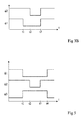
- the Figures 3A and 3B are timing diagrams illustrating in more detail an example of a control method of the sensor of the figure 1 .
- the sensor pixels are read line by line at low-resolution (1-bit), the set of lines being scanned OSR times so as to provide OSR images of 1-bit per pixel.
- a final high-resolution image is reconstructed by the digital filtering circuits, from the OSR binary images.
- the integration phases of all the pixels of the sensor start simultaneously, and the low-resolution quantization steps of the integrated signal (via the converter digital analogue formed by the comparator 102 and the flip-flop 104), the digital-to-analog conversion of the low-resolution signal (via the circuit 106), and the subtraction of the feedback signal to the integrated signal (via the circuit 106) are performed simultaneously for all the pixels of the sensor.
- FIG. 3A represents the evolution, as a function of time, of the clock signal clk (common to all the pixels of the sensor), and of the control signals V RS1 , V RS2 , V RS3 ,..., V RSM , respectively applied on the control knots of the selection switches RS of the pixels of the M rows of the sensor.
- Each period of the clock signal clk, of duration T OSR, which corresponds to an acquisition phase of a binary image (for example between two successive rising edges of the clock signal CLK) is divided into M successive periods T RD1 , T RD2 , T RD3 , ..., T RDM , for example equal to T OSR / M.
- T RDm one of the pixel lines of the sensor is activated in reading, by the closing of the selection switches RS of the pixels of the line (signal V RSm of the line in the high state in this example), the selection switches RS of the pixels of the other lines of the sensor being kept open.
- the binary output values of the N pixels of the line are read simultaneously, via the conductive tracks CL n , by the filter circuits coupled to the tracks CL n .
- a digital-to-analog conversion phase of the output signal of the flip-flop 104, and of feedback of the analog signal resulting in the integrator formed by the photodiode is implemented simultaneously in all the pixels of the sensor, via the respective circuits 106 of the pixels.
- This phase which we will be referred to below as the feedback phase, is detailed in figure 3B .
- the figure 3B illustrates more particularly the evolution, as a function of time, of the control signals ⁇ 1 and ⁇ 2 (common to all the pixels of the sensor) of the circuits 106 of the pixels of the sensor.
- the signal ⁇ 2 is first set high, resulting in the transistor 111 being non-conducting. .
- the signal ⁇ 1 is also set high, which causes the accumulation of positive charges under the gate of the PMOS transistor 113.
- the signal ⁇ 1 is set low, the signal ⁇ 2 is kept high, which results in a quantity of positive charges Q DAC ⁇ C [0114] W 113 * L 113 * (V b1 -V b2 ), isolated from the signal application node ⁇ 1, remains trapped under the gate of transistor 113, where C ox113 , W 113 and L 113 respectively denote the defined capacity per unit area by the gate oxide of transistor 113, the gate width of transistor 113, and the gate length of transistor 113.
- the signal ⁇ 2 is set low, the signal ⁇ 1 being kept low.
- the transistor 111 is turned on, which causes the transfer, on the node K, of the load packet Q DAC stored in the gate of the transistor 113.
- the output of the flip-flop 104 is in the high state (V pix > v ref )
- the transistor 111 remains off, and no charge is injected into the photodiode by the circuit 106.
- the signals ⁇ 1 and ⁇ 2 are reset, so as to recharge the feedback circuit 106 with a view to the next feedback phase.
- An advantage of the sensor described in connection with Figures 1, 2, 3A and 3B is that, because of the synchronous nature of the rolling shutter type of reading, the digital filtering circuits of the digital analog converters can be deported outside the pixels, and shared by several pixels of the sensor. In addition, the output signals of the pixels are digital signals, and are therefore relatively robust to parasitic disturbances and technological non-idealities.
- an asynchronous architecture can be provided in which the output of the comparator 102 is connected to the transistor 111 by an intermediate circuit making it possible to generate a voltage pulse when the voltage V pix of the node K goes below the reference voltage V ref.
- the flip-flop 104 is no longer on the feedback path of the modulator, and may be an asynchronous flip-flop.
- This rocker makes it possible to store the event, if it occurred during a period T OSR , to be read synchronously during a reading of type "rolling shutter" (the rocker being then reset at the end of each period T OSR ).
- An example of this intermediate circuit for load-asynchronous reset is presented in the aforementioned article A.
- a sigma-delta modulator of order p, with p integer greater than 1, differs from a first-order sigma-delta modulator essentially in that it comprises not just one but p analog integrators, generally connected in series with one another. upstream of the low-resolution analog-to-digital converter.
- the feedback signal of the modulator can be fed back either to the input of the first integrator only, or to the input of the first integrator and to the input of one or more of the following integrators, possibly with different weighting coefficients.
- the replacement of a modulator of order 1 by a modulator of order 2 makes it possible to reduce the OSR by a factor of about 10 , without decreasing the signal-to-noise ratio.
- an OSR of about 100 would be sufficient, which would make it possible to reduce by approximately a factor of 10 the scanning frequency of the sensor in an architecture of the type described in relation to the Figures 1, 2, 3A and 3B .
- the sigma-delta modulators are all the more cumbersome that their order is high, especially because of the increase in the number of analog integrators they comprise.
- the integration of a high order sigma-delta modulator within a pixel of an image sensor can therefore be problematic.
- the figure 4 is a partial circuit diagram of an example of an embodiment of a CMOS image sensor.
- the sensor of the figure 4 includes a plurality of identical pixels or the like, for example arrayed in rows and columns.
- the pixels are interconnected in pairs.
- MxN pixels P m, n where M * N is an even number.
- This sensor has M * N / 2 groups of two interconnected pixels.
- the pixels of the same group are preferably neighbors.
- the pixels of the same group are preferably arranged so that they can be read simultaneously.
- the pixels can be activated in line-by-line reading, and the pixels of the same group of interconnected pixels are pixels that are neighbors of the same pixel line (in this example, the number N of columns of pixels of the sensor is even).
- the pixels P m, n and P m, n + 1 of the same group of interconnected pixels, belonging to the same line of row m of the sensor and to neighboring columns of ranks n and n + 1 have been represented on the figure 4 .
- each pixel of the sensor of the figure 4 substantially comprises the same elements as a sensor pixel of the figure 1 , namely a photodiode 100, a comparator 102, a synchronous storage circuit 104, a feedback circuit 106, and a selection switch RS, arranged in substantially the same manner as in the example of FIG. figure 1 .
- a photodiode 100 a photodiode 100
- a comparator 102 a synchronous storage circuit 104
- a feedback circuit 106 a selection switch RS
- Each pixel of the sensor of the figure 4 further comprises a configurable link circuit 401 for connecting the first-order sigma-delta modulator of the pixel to the first-order sigma-delta modulator of the other pixel of the same group of interconnected pixels so as to form a 2.
- the link circuit 401 comprises three N-channel MOS transistors 411, 413 and 415 connected in series between the node K of the pixel and an application node of a signal of FIG. binary command ⁇ 3, for example a voltage.
- transistor 411 has a first conduction node connected to node K of the pixel and a second a conduction node connected to a first conduction node of the transistor 413
- the transistor 413 has a second conduction node connected to a first conduction node of the transistor 415
- the transistor 415 has a second conduction node connected to the application node of the voltage ⁇ 3.
- the transistor 415 has its control gate connected to the node K of the other pixel of the same group of interconnected pixels.
- Transistor 413 has its control gate connected to an application node of a fixed bias voltage V b3 .
- the circuit 401 further comprises an AND gate 417 with two inputs and an output.
- the output of the gate 417 is connected to the control gate of the transistor 411, a first input of the gate 417 is connected to an application node of a binary control signal ⁇ 2 complementary signal ⁇ 2 (the first input of the gate 417 is for example connected to the application node of the control signal ⁇ 2 via an inverter not shown), and the second input of the gate 417 is connected to a application node of a configuration binary signal, for example a voltage.
- the binary configuration signals of the first and second pixels of the same group of interconnected pixels are controllable independently of one another, and are respectively designated by the references m B for a first pixel of the group (the pixel P m, n in the example shown) and m A for the other pixel of the group (the pixel P m, n + 1 in the example shown).
- the logic signals of configuration m A and m B are common to all the interconnected pixel groups of the sensor.
- the bias voltages V b1 , V b2 and V b3 are common to all the pixels of the sensor, and the control signals ⁇ 1, ⁇ 2 and ⁇ 3, as well as the clock signal clk, are common. to all the pixels of the sensor.
- the transistors 411 of the link circuits 401 of the pixels P m, n and P m, n + 1 are non-conducting, and the sigma-delta modulators of 1 order of pixels P m, n and P m, n + 1 are thus isolated from the other.
- the first-order sigma-delta modulators of the first and second pixels of the group operate independently.
- the sensor can then operate identically or similarly to what has been described in connection with the Figures 1, 2, 3A and 3B .
- the transistor 411 of the link circuit 401 of the pixel P m, n is kept blocked whatever the state of the signal of command ⁇ 2.
- the transistor 411 of the link circuit of the pixel P m, n + 1 can be turned on via the control signal ⁇ 2 .
- the link circuit 401 of the pixel P m, n + 1 then makes it possible to inject, in the integrator of the sigma-delta modulator of order 1 of the pixel P m, n + 1 , that is to say on the node K of the pixel P m, n + 1 , a signal representative of the quantization error of the modulator of order 1 of the pixel P m, n .
- the first-order sigma-delta modulators of the pixels P m, n and P m, n + 1 then together form a sigma-delta modulator of order 2.
- Such a second-order sigma-delta modulator constituted by putting in series two first-order modulators each comprising an analog integrator, a low-resolution analog-digital converter, and a feedback loop, is generally called a MASH modulator.
- MASH modulator Multi Stage Noise Shaping
- Multi-stage noise shaping modulator The operating principle of sigma-delta modulators of the MASH type is for example described in the article " Sturdy MASH ⁇ - ⁇ modulator "by Maghari et al. (ELECTRONICS LETTERS 26th October 2006 Vol.42 No.22 ), the content of which is considered an integral part of this description.
- a first first-order modulator receives the analog signal to be digitized on its analog input
- the second first-order modulator receives on its analog input a signal representative of the quantization error of the first modulator of order 1.
- each of the order 1 modulators provides a train of OSR bits output of its low-resolution analog-digital converter, the two bitstreams being recombined into a single bit OSR train by a digital recombination circuit, then digitally integrated by a digital filtering circuit generating, from the recombined bit stream, a high-resolution digital value representative of the modulator input analog signal upstream.
- the topologies of the MASH type are available regardless of the order of the elementary modulators connected in series, and regardless of the number of elementary modulators connected in series.
- each modulator of the series association of elementary modulators receives on its analog input a signal representative of the quantization error of the preceding modulator.
- One advantage of sigma-delta modulators of the MASH type is that they make it possible to obtain high modulation orders, by avoiding the problems usually encountered (notably problems of instability) in the production of traditional sigma-delta modulators. high order (with several analog integrators in series but only one analog-to-digital converter and one feedback loop).
- the first order modulator of the pixel P m, n is the upstream modulator of the MASH structure.
- each of the first-order modulators of the pixels P m, n and P m, n + 1 provides a bit stream via the output track CL n , respectively CL n + 1 , of the pixel.
- the two bitstreams can be recombined in a single bit stream via a recombination circuit, not shown, for example arranged at the foot of the column.
- the recombined bitstream is then provided to a digital filter circuit adapted to produce a high-resolution digital output value representative of the illumination levels received by the pixels P m, n and P m, n + 1 , weighted by different coefficients. More particularly, for the group comprising the pixels P m, n and P m, n + 1 , a high resolution digital output value representative of the signal ⁇ I (P m, n ) + ⁇ I (P m, n + 1 ) is obtained.
- I (P m, n ) and I (P m, n + 1 ) respectively denote the luminous intensity received by the pixel P m, n and the luminous intensity received by the pixel P m, n + 1 , and where ⁇ and ⁇ are distinct weighting coefficients, with ⁇ > ⁇ (the level of illumination received by the group's upstream pixel is preponderant compared to the level of illumination received by the group's downstream pixel in the value output of the 2nd order sigma-delta converter).
- the recombination circuits and the digital filter circuits have not been described, the described embodiments being compatible with the usual recombination and digital filtering circuits used in existing sigma-delta converters.
- the operation is similar to what has just been described, with the difference that the sigma-delta modulator of order 1 of the pixel P m, n + 1 is upstream of the first-order sigma-delta modulator of the pixel P m, n in the MASH structure.
- the high-resolution digital output value of the sigma-delta converter is then representative of the signal ⁇ I (P m, n + 1 ) + ⁇ I (P m, n ).
- a first acquisition phase of a partial digital image of size M * N / 2 can be provided, during which the configuration signals m A and m B are respectively in the high state and in the low state. .
- a high resolution digital output value representative of the signal ⁇ I (P1) + ⁇ I (P2) is acquired.
- a second phase of acquisition of a partial digital image of size M * N / 2 can then be implemented, in which the configuration signals m A and m B are respectively in the low state and in the high state (that is to say that, in each group of pixels, the upstream pixel and the downstream pixel are inverted).
- each of the first and second acquisition phases of a partial image of size M * N / 2 includes successive OSR scans of the M lines of the sensor.
- the acquisition of a complete image comprises 2 * OSR successive sweeps of the M lines of the sensor.
- the transition from a first-order sigma-delta modulator to a second-order sigma-delta modulator makes it possible to reduce the OSR by a significant factor, for example by a factor of 10 , without decreasing the signal-to-noise ratio at the output of the analog-to-digital converter.
- the scanning frequency of the sensor lines can be reduced by a factor of 5 with respect to a sensor having the same number of lines but performing a sigma-delta analog-to-digital conversion of order 1, for example a sensor of the type described in connection with the figure 1 .
- These orders of magnitude are of course illustrative and in no way limiting.
- each point of the image of size M * N / 2 has a value representative of both the illumination of the first pixel of the corresponding group of interconnected pixels, and the illumination of the second pixel of the group of pixels. interconnected. This allows for example to increase by a factor of 2 the rate of acquisition of images.
- control method of the sensor of the figure 4 corresponds to a first phase of acquiring a partial image of size M * N / 2, the sensor being configured to perform a sigma-delta analog-digital conversion.
- the configuration signals m A and m B are respectively in the high state and in the low state.
- An identical or similar control method may, however, be implemented during the acquisition phase of the second part of the image (the configuration signals m A and m B then being respectively in the low state and at the high state).
- the sensor pixels are read line by line at low resolution (1-bit), the set of lines being scanned OSR times so as to provide, for each group of interconnected sensor pixels, two trains of OSR bits.
- the two trains of OSR bits are recombined by a not shown recombination circuit, in a single train of OSR bits representative of both the photocurrent generated in the photodiode of the upstream pixel of the group (the pixel P m, n in the example shown) and the photocurrent generated in the photodiode of the pixel of the downstream group (the pixel P m, n + 1 in this example).
- a high resolution digital output value of the group comprising the pixels P m, n and P m, n + 1 is produced, from this recombined bitstream, by the digital filter circuits (not shown).
- the integration phases of all the pixels of the sensor start simultaneously, and the low-resolution quantization phases of the analog signals, as well as the feedback phases (including the transfer of the quantization error of the modulator of order 1 upstream in the analog integrator of the modulator of order 1 downstream), are carried out simultaneously in all groups of pixels of the sensor.
- each period of the clock signal clk of duration T OSR (for example between two successive rising edges of the clock signal clk), is divided into M successive periods T RD1 , T RD2 , T RD3 , ..., T RDM , for example equal to T OSR / M.
- T RDm one of the pixel lines of the sensor is activated in reading, by the closing of the selection switches RS of the pixels of the line (signal V RSm of the line in the high state in this example), the selection switches RS of the pixels of the other lines of the sensor being kept open.
- the binary output values of the N pixels of the line are read simultaneously, via the conductive tracks CL n , by the filter circuits coupled to the tracks CL n .
- a phase which will be called hereinafter feedback phase, is implemented simultaneously in all groups of interconnected pixels of the sensor.
- the output signal of the low-resolution analog-to-digital converter of the pixel i.e., the output signal of flip-flop 104 of the pixel
- the output signal of flip-flop 104 of the pixel is converted into an analog signal and subtracted from the integrated signal by the pixel photodiode (via the circuit 106 of the pixel).
- a signal representative of the signal integrated in the photodiode of the group's upstream pixel (the pixel P m, n in this example) is injected into the photodiode of the group's downstream pixel (the pixel P m , n + 1 in this example), via the link circuit 401 of the downstream pixel.
- the figure 5 is a chronogram illustrating in more detail the progress of the feedback phase.
- the figure 5 schematically represents the evolution, as a function of time, of the control signals ⁇ 1, ⁇ 2 and ⁇ 3 (common to all the pixels of the sensor) of the circuits 106 and 401 of the pixels of the sensor, during the feedback phase.
- the signals ⁇ 1 and ⁇ 2 are set high, and the signal ⁇ 3 is set low.
- the transistors 111 and 411 are in the off state.
- positive charges (holes) accumulate under the gate of the transistor 113
- negative charges (electrons) accumulate under the gate of the NMOS transistor 413.
- the signals ⁇ 1 and ⁇ 3 are respectively set low and high, the signal ⁇ 2 being kept high.
- a quantity of positive charges Q DAC ⁇ C ox113 * W 113 * L 113 * (V b1 -V b2 ), isolated from the application node of the signal ⁇ 1 remains trapped under the gate of transistor 113.
- a quantity of negative charges Q A proportional to U pixB -U b3 (approximately equal to C ox413 * W 413 * L 413 * (V pixB -V b3 ), where C ox413 , W 413 and L 413 respectively denote the surface capacity defined by the gate oxide of transistor 413, the gate width of the transistor 413, and the gate length of the transistor 413, and where V pixB designates the potential of the node K of the downstream pixel, that is to say of the pixel P m, n + 1 in this example), isolated from the node for applying the signal ⁇ 3, remains trapped under the gate of the transistor 413.
- a quantity of negative charges Q B proportional to V pixA -V b3 (approximately equal to C ox413 * W 413 * L 413 *, where V pixA denotes the potential of the node K of the upstream pixel, that is to say the pixel P m, n in this example ), isolated from the application node of the signal ⁇ 3, remains trapped under the gate of the transistor 413.
- the signal ⁇ 2 is set low, the signals ⁇ 1 and ⁇ 3 are maintained respectively in the low state and in the high state.
- the transistor 111 of the pixel is turned on, which causes the transfer, on the node K of the pixel of the charge packet Q DAC stored under the gate of the transistor 113 of the pixel.
- the transistor 111 remains non-conducting, and no charge is injected into the photodiode by the circuit 106.
- the transistor 411 of the downstream pixel of the modulator sigma-delta modulator 2 (the pixel P m, n + 1 in the example shown) is turned on, which causes the transfer, on the node K the downstream pixel, the amount of negative charges stored under the gate of transistor 413 of this pixel (proportional to the signal integrated in the photodiode of the upstream pixel, representative of the quantization error of the first-order modulator of the upstream pixel).
- the transistor 411 of the upstream pixel of the modulator of order 2 (the pixel P m, n in this example) remains blocked, and no charge is injected into the photodiode of this pixel via the circuit 401 of this pixel.
- the signal ⁇ 2 is again set high so as to isolate, in each pixel of the sensor, the charge injection circuits. 106 and 401 of the pixel node K.
- the signals ⁇ 1 and ⁇ 3 can be reset respectively to the high state and the low state, so as to recharge the circuits 106 and 401 in order to the next phase of feedback.
- the coefficients of the modulator of order 2 can be fixed by the size of the transistors 113 and 413 of the charge injection circuits 106 and 401.
- the transistors 113 and 413 can have separate charge storage capacities.
- the charge storage capacity of the transistor 413 can be chosen relatively high, so that, during the feedback phase, the amount of negative charges injected into the photodiode 100 of the downstream pixel of the modulator of order 2, by the link circuit 401 of this pixel is preponderant in front of the amount of photogenerated charges in the photodiode of this pixel at each period T OSR .
- the embodiment of the figure 4 has the advantage of enabling, without significantly increasing the size and the complexity of the pixels of the sensor, to significantly reduce the scanning frequency of the pixels with respect to a sensor of the type described in connection with the figure 1 (with identical image acquisition time, identical quantization resolutions, and identical quantization noise levels).
- each pixel comprises a first-order sigma-delta modulator, the pixels being interconnected in groups of two pixels, the modulators of the pixels of the same group being connectable to form a modulator of order 2. More generally, according to an aspect of the embodiments described, each pixel comprises a modulator of order p equal to or greater than 1, and the pixels are interconnected in groups of q pixels, with q equal to or greater than 2, the pixels of the same group being be connected to form a modulator of order p * q.
- the described embodiments are not limited to the particular examples of feedback circuits 106 and link 401 described in connection with the figure 4 .
- those skilled in the art will be able to adapt the described embodiments to replace the feedback circuits 106 and link 401 described in connection with the figure 4 by other circuits, for example circuits adapted to recharge in voltage, respectively discharge in current, the node K of the pixel.
- the embodiments described are not limited to the particular case described above in which, in each pixel of the sensor, the analog integrator of the sigma-delta modulator of the pixel comprises the photodiode of the pixel.
- the analog integrator of the sigma-delta modulator of the pixel comprises the photodiode of the pixel.
- one or more specific additional capabilities may be provided in each pixel to form the analog integrator of the sigma-delta modulator of the pixel.
- low-resolution analog-to-digital converter comprising a comparator 102 and a flip-flop 104 connected at the output of the comparator 102.
- low-resolution analog-to-digital converter can be constituted by a 1-bit comparator directly driven by a clock signal, or, more generally, by any other suitable low-resolution analog-to-digital conversion circuit.
Landscapes
- Engineering & Computer Science (AREA)
- Theoretical Computer Science (AREA)
- Multimedia (AREA)
- Signal Processing (AREA)
- Analogue/Digital Conversion (AREA)
- Compression, Expansion, Code Conversion, And Decoders (AREA)
- Transforming Light Signals Into Electric Signals (AREA)
Abstract
Description
- La présente demande concerne le domaine des circuits électroniques de façon générale, et vise plus particulièrement le domaine des capteurs d'images CMOS.
- De façon classique, un capteur d'images CMOS comprend une pluralité de cellules élémentaires ou pixels identiques ou similaires agencés en matrice selon des lignes et des colonnes. Chaque pixel comprend un photodétecteur, par exemple une photodiode polarisée en inverse dont la capacité de jonction est déchargée par un photocourant en fonction d'une intensité lumineuse reçue. Chaque pixel comprend en outre un circuit de lecture adapté à fournir un signal de sortie représentatif de l'intensité lumineuse reçue par le photodétecteur. Traditionnellement, chaque pixel fournit, via son circuit de lecture, un signal de sortie analogique, par exemple une tension ou un courant. Ce signal est ensuite numérisé à l'extérieur du pixel par un circuit de conversion analogique-numérique. Le circuit de conversion analogique-numérique peut être commun à plusieurs pixels du capteur. Par exemple, dans le cas où les pixels sont lus ligne par ligne, c'est-à-dire dans le cas où tous les pixels d'une même ligne sont lus simultanément et où les pixels de lignes distinctes sont lus séquentiellement, le capteur peut comprendre un circuit de conversion analogique-numérique par colonne de pixels.
- On a déjà proposé des architectures de capteurs d'images CMOS dans lesquelles chaque pixel comprend tout ou partie d'un convertisseur analogique-numérique de type sigma-delta. Des exemples de telles architectures sont décrites dans les articles "Pixel-level A/D conversion: comparison of two charge packets counting techniques", de A. Peizerat et al., ci-après appelé article A, et "Low-Power, High Dynamic Range CMOS Image Sensor Employing Pixel-level Oversampling ΣΔ Analog-to-Digital Conversion", ci-après appelé article B, dont les contenus respectifs sont considérés comme faisant partie intégrante de la présente description.
- Rappelons d'abord la structure générale d'un convertisseur analogique-numérique de type sigma-delta. Un tel convertisseur comprend typiquement un modulateur sigma-delta recevant un signal analogique d'entrée à numériser et fournissant, à une fréquence relativement élevée, une suite d'échantillons numériques intermédiaires à basse résolution (typiquement des échantillons binaires) représentatifs du signal d'entrée. La sortie du modulateur sigma-delta est reliée à un circuit de filtrage numérique et de décimation, qui reçoit les échantillons numériques intermédiaires fournis par le modulateur, et fournit des échantillons numériques haute-résolution (supérieure à la résolution des échantillons de sortie du modulateur) représentatifs du signal analogique d'entrée, à une fréquence inférieure à la fréquence de fourniture des échantillons intermédiaires par le modulateur sigma-delta. Le nombre d'échantillons basse-résolution utilisés pour produire une valeur numérique de sortie haute-résolution est généralement désigné par l'acronyme OSR, de l'anglais "Over Sampling Ratio" (taux de sur-échantillonnage).
- De façon classique, un modulateur sigma-delta d'ordre 1 comprend un intégrateur analogique, typiquement une capacité, et, en sortie de l'intégrateur, un convertisseur analogique-numérique basse-résolution, typiquement un comparateur 1-bit. Le signal analogique d'entrée du modulateur (le signal à numériser) est appliqué en entrée de l'intégrateur, la sortie du convertisseur analogique-numérique basse-résolution formant la sortie du modulateur sigma-delta. La sortie du convertisseur analogique-numérique basse résolution est en outre reliée à l'entrée de l'intégrateur par l'intermédiaire d'une boucle de rétroaction comportant un convertisseur numérique-analogique basse-résolution. Plus particulièrement, le signal analogique fourni par la boucle de rétroaction est soustrait au signal analogique d'entrée au niveau de l'intégrateur, de façon que l'intégrateur intègre un signal représentatif de l'erreur de quantification du convertisseur analogique-numérique basse-résolution.
- Les convertisseurs analogique-numérique de type sigma-delta peuvent être utilisés pour diverses raisons, et notamment parce qu'ils présentent un encombrement et une consommation électrique relativement faibles, et sont robustes aux non-idéalités des composants. De plus, dans le domaine des capteurs d'images, les convertisseurs sigma-delta permettent d'étendre la plage dynamique des pixels.
- Dans l'article A susmentionné, chaque pixel comprend un modulateur sigma-delta d'ordre 1 asynchrone, dont l'intégrateur est constitué par une capacité déchargée par un photocourant produit par la photodiode du pixel. Le convertisseur analogique-numérique basse-résolution est constitué par un comparateur comparant la tension aux bornes de la capacité d'intégration à une tension de référence, et fournissant un signal de sortie binaire représentatif du résultat de cette comparaison. La sortie du comparateur constitue la sortie numérique du modulateur. La sortie du comparateur pilote de plus un circuit d'injection de charges qui forme la boucle de rétroaction du modulateur. Plus particulièrement, chaque fois que la tension aux bornes de la capacité d'intégration passe sous la tension de référence, la sortie du comparateur commande l'injection de charges positives dans la capacité d'intégration, de façon à recharger cette capacité à une tension supérieure à la tension de référence. Deux types de circuits de rétroaction sont proposés dans l'article A, à savoir un circuit réalisant une rétroaction en tension (la capacité d'intégration est réinitialisée à un niveau de tension prédéterminé), et un circuit réalisant une rétroaction en charges (une quantité de charges prédéterminée est injectée dans la capacité d'intégration). La sortie du comparateur est reliée à un compteur asynchrone externe au modulateur sigma-delta (circuit de filtrage numérique), qui compte le nombre de fois que la tension de la capacité d'intégration passe sous la tension de référence pendant une période d'intégration du pixel.
- Dans une architecture du type décrit dans l'article A, du fait de la nature asynchrone du modulateur sigma-delta, il est en pratique nécessaire que chaque pixel comporte son propre circuit de filtrage numérique, ce qui pose problème du fait de l'encombrement relativement important des compteurs numériques.
- Dans l'article B susmentionné, chaque pixel comprend une partie seulement d'un modulateur sigma-delta d'ordre 1, l'autre partie du modulateur étant commune à plusieurs pixels du capteur. Plus particulièrement, dans l'article B, chaque pixel comprend un intégrateur, formé par la capacité de jonction de la photodiode du pixel, et un circuit de rétroaction pour réinitialiser en charges la photodiode du pixel, c'est-à-dire pour injecter une quantité de charges prédéterminée dans la photodiode. Le convertisseur analogique-numérique basse-résolution, un comparateur 1-bit, est externe au pixel, et est partagé par plusieurs pixels du capteur. Plus particulièrement, dans l'article B, les pixels sont sélectionnables en lecture ligne par ligne, et le capteur comprend un comparateur de courant 1-bit par colonne de pixels. Dans chaque pixel, la sortie analogique de l'intégrateur est reliée à l'entrée du comparateur par l'intermédiaire d'un transistor monté en source de courant (la grille de ce transistor étant connectée à la sortie en tension de l'intégrateur), d'un transistor de sélection, et d'une piste conductrice de sortie du pixel, commune à tous les pixels de la colonne. De plus, dans chaque pixel, un noeud de commande du circuit de rétroaction est relié à la sortie numérique (binaire) du comparateur par l'intermédiaire d'une piste conductrice commune à tous les pixels de la colonne. Le circuit d'injection de charges forme le convertisseur numérique-analogique basse-résolution de la boucle de rétroaction du modulateur sigma-delta. Le capteur comprend en outre un circuit de filtrage par colonne de pixels, en aval du comparateur 1-bit de la colonne.
- Dans l'article B, les modulateurs sigma-delta ont un fonctionnement synchrone, c'est-à-dire que le convertisseur analogique-numérique basse-résolution est piloté par un signal d'horloge, la sortie binaire du convertisseur basse-résolution étant apte à changer d'état uniquement sur une impulsion ou un front du signal d'horloge.
- Un inconvénient de l'architecture décrite dans l'article B est que les signaux de sortie des pixels sont des signaux analogiques (courants), et sont donc relativement peu robustes aux perturbations parasites.
- Par ailleurs, un autre inconvénient de l'architecture décrite dans l'article B est que la cadence de lecture des données de sortie des pixels est relativement élevée. A titre d'exemple illustratif, pour produire des échantillons numériques de sortie sur 10-bits avec un rapport signal sur bruit satisfaisant, il convient de prévoir un OSR de l'ordre de 210 = 1024 (c'est-à-dire 1024 lectures par pixel). Dans le cas d'un capteur de 500 lignes dans lequel les pixels sont lus ligne par ligne, et pour une fréquence d'acquisition de 50 images par seconde, la fréquence de balayage des lignes est alors de l'ordre de f = 50 * 500 * 210 = 25,6 MHz. Une telle fréquence de lecture entraine une consommation électrique relativement élevée, et peut conduire à des erreurs de lecture, notamment dans le cas d'une architecture du type décrit dans l'article B, dans laquelle les signaux de sortie des pixels sont des signaux analogiques.
- Il serait souhaitable de pouvoir disposer d'un capteur d'images CMOS à conversion analogique-numérique sigma-delta, ce capteur palliant tout ou partie des inconvénients des capteurs existants.
- Ainsi, un mode de réalisation prévoit un capteur d'images CMOS comportant une pluralité de pixels comprenant chacun : une photodiode ; un modulateur sigma-delta d'ordre p, avec p entier supérieur ou égal à 1, adapté à fournir un signal numérique binaire représentatif du niveau d'éclairement de la photodiode ; et un circuit configurable de liaison permettant de relier le modulateur sigma-delta du pixel à un modulateur sigma-delta d'un autre pixel, de façon que les modulateurs des deux pixels forment ensemble un modulateur sigma-delta d'ordre supérieur à p.
- Selon un mode de réalisation, les pixels sont répartis par groupes de q pixels, avec q entier supérieur ou égal à 2, les pixels d'un même groupe étant interconnectés et les circuits de liaison des pixels d'un même groupe pouvant être configurés pour relier les modulateurs d'ordre p des pixels du groupe de façon que ces modulateurs forment ensemble un modulateur sigma-delta d'ordre q*p.
- Selon un mode de réalisation, dans chaque pixel, le modulateur sigma-delta d'ordre p du pixel comprend un intégrateur analogique comportant la photodiode du pixel.
- Selon un mode de réalisation, dans chaque pixel, le modulateur sigma-delta d'ordre p comprend un convertisseur analogique-numérique d'un signal analogique de sortie de l'intégrateur analogique du pixel.
- Selon un mode de réalisation, dans chaque pixel, le convertisseur analogique-numérique comprend un comparateur comparant ledit signal de sortie à un signal de référence.
- Selon un mode de réalisation, dans chaque pixel, le modulateur sigma-delta d'ordre p comprend un circuit de rétroaction reliant un noeud de sortie du convertisseur analogique-numérique à un noeud de l'intégrateur analogique du pixel.
- Selon un mode de réalisation, dans chaque pixel, le circuit de rétroaction est adapté à injecter une quantité de charges prédéterminée dans l'intégrateur analogique du pixel.
- Selon un mode de réalisation, les charges sont de signe opposé à celui des charges photogénérées accumulées dans la photodiode du pixel.
- Selon un mode de réalisation, dans chaque pixel, le circuit de rétroaction comprend des premier, deuxième et troisième transistors MOS à canal P en série entre le noeud de l'intégrateur analogique du pixel, et un noeud d'application d'un premier signal de commande.
- Selon un mode de réalisation, dans chaque pixel, les grilles de commande des deuxième et troisième transistors MOS à canal P sont reliées respectivement à des premier et deuxième potentiels de polarisation.
- Selon un mode de réalisation, dans chaque pixel, la grille de commande du premier transistor MOS à canal P est reliée à un noeud d'application d'un deuxième signal de commande et audit noeud de sortie du convertisseur analogique-numérique par l'intermédiaire d'une porte logique.
- Selon un mode de réalisation, dans chaque pixel, le circuit de liaison est adapté à injecter, sur un noeud de l'intégrateur analogique du pixel, une quantité de charges représentative d'un signal de sortie de l'intégrateur analogique d'un autre pixel du capteur.
- Selon un mode de réalisation, dans chaque pixel, le circuit de liaison comprend des premier, deuxième et troisième transistors MOS à canal N en série entre le noeud de sortie de l'intégrateur analogique du pixel et un noeud d'application d'un troisième signal de commande.
- Selon un mode de réalisation, dans chaque pixel, les grilles de commande des deuxième et troisième transistors MOS à canal N sont reliées respectivement à un troisième potentiel de polarisation et à un noeud d'un intégrateur analogique d'un autre pixel du capteur.
- Ces caractéristiques et avantages, ainsi que d'autres, seront exposés en détail dans la description suivante de modes de réalisation particuliers faite à titre non limitatif en relation avec les figures jointes parmi lesquelles :
- la
figure 1 est un schéma électrique partiel d'un exemple d'un capteur d'images CMOS ; - la
figure 2 est un chronogramme représentant l'évolution d'une tension analogique aux bornes d'une photodiode d'un pixel du capteur de lafigure 1 ; - les
figures 3A et3B sont des chronogrammes illustrant un exemple de procédé de commande du capteur de lafigure 1 ; - la
figure 4 est un schéma électrique partiel d'un exemple d'un mode de réalisation d'un capteur d'images CMOS ; et - la
figure 5 est un chronogramme illustrant un exemple de procédé de commande du capteur de lafigure 4 . - Par souci de clarté, de mêmes éléments ont été désignés par de mêmes références aux différentes figures et, de plus, les divers chronogrammes ne sont pas tracés à l'échelle. On notera par ailleurs que dans la présente description, lorsque des architectures de pixels ou de capteurs d'images sont décrites, on utilise le terme "connecté" pour désigner une liaison électrique directe, sans composant électronique intermédiaire, par exemple au moyen d'une piste conductrice, et le terme "couplé" ou le terme "relié", pour désigner une liaison électrique directe ou via un ou plusieurs composants intermédiaires, par exemple via un ou plusieurs transistors MOS.
- La
figure 1 est un schéma électrique partiel d'un exemple d'un capteur d'images CMOS. Le capteur de lafigure 1 comprend une pluralité de pixels identiques ou similaires. A titre d'exemple, le capteur de lafigure 1 comprend M*N pixels Pm,n agencés en matrice selon M lignes et N colonnes, avec M et N entiers supérieurs à 1, m entier allant de 1 à M, et n entier allant de 1 à N. Sur lafigure 1 , par souci de simplification, seul un pixel Pm,n du capteur a été représenté. - Le pixel Pm,n comprend une photodiode 100 polarisée en inverse, dont l'anode est connectée à un noeud d'application d'un potentiel de référence GND, par exemple la masse, et dont la cathode est connectée à un noeud K d'accumulation de charges photogénérées. Le pixel Pm,n comprend en outre un comparateur 102 à deux entrées analogiques et une sortie binaire. Une entrée (+) du comparateur 102 est connectée au noeud K, et l'autre entrée (-) du comparateur 102 est connectée à un noeud d'application d'une tension de référence Vref. Le comparateur 102 comprend par exemple un amplificateur opérationnel monté en comparateur de tension, dont une entrée inverseuse est reliée au noeud d'application du potentiel de référence Vref, et dont une entrée non inverseuse est reliée au noeud K. La sortie du comparateur est reliée à une entrée de données binaires D d'une bascule 104. Dans l'exemple représenté, la bascule 104 du pixel Pm,n comprend en outre une entrée d'application d'un signal d'horloge clk, et une sortie de données binaires Q. Le fonctionnement du circuit 104 est tel que, à chaque front montant ou à chaque front descendant du signal d'horloge clk, la donnée binaire présente sur l'entrée D de la bascule 104 est recopiée sur sa sortie Q. Le pixel Pm,n comprend en outre un circuit 106 d'injection de charges positives sur le noeud d'accumulation K de la photodiode 100. Le circuit 106 comprend trois transistors MOS à canal P 111, 113 et 115 connectés en série entre le noeud K et un noeud d'application d'un signal de commande binaire Φ1, par exemple une tension. Plus particulièrement, dans cet exemple, le transistor 111 a un premier noeud de conduction connecté au noeud K et un deuxième noeud de conduction connecté à un premier noeud de conduction du transistor 113, le transistor 113 a un deuxième noeud de conduction connecté à un premier noeud de conduction du transistor 115, et le transistor 115 a un deuxième noeud de conduction connecté au noeud d'application de la tension Φ1. Le transistor 115 a sa grille de commande reliée à un noeud d'application d'une tension de polarisation fixe Vb1, et le transistor 113 a sa grille de commande reliée à un noeud d'application d'une tension de polarisation fixe Vb2. Le circuit 106 comprend en outre une porte logique OU 117 à deux entrées et une sortie, dont la sortie est reliée à la grille de commande du transistor 111, et dont les entrées sont reliées respectivement à la sortie Q de la bascule 104 et à un noeud d'application d'un signal binaire de commande Φ2, par exemple une tension.
- Ainsi, dans l'exemple de la
figure 1 , chaque pixel Pm,n du capteur comprend un modulateur sigma-delta d'ordre 1 synchrone, dont l'intégrateur est formé par la capacité de la photodiode 100 du pixel. Le comparateur 102 et la bascule 104 forment le circuit de conversion analogique-numérique basse-résolution (1-bit) du modulateur. Le circuit 106 ou circuit de rétroaction forme la boucle de rétroaction du modulateur. - Le pixel Pm,n comprend en outre un interrupteur de sélection RS, par exemple un transistor MOS, reliant la sortie Q de la bascule 104, c'est-à-dire la sortie du modulateur sigma-delta, à une piste conductrice de sortie CLn commune à tous les pixels de la colonne de rang n du capteur.
- Dans cet exemple, les pixels du capteur de la
figure 1 sont activables en lecture ligne par ligne, c'est-à-dire notamment que tous les interrupteurs de sélection RS des pixels Pm,n d'une même ligne ont leurs noeuds de commande reliés à un même noeud d'application d'un signal de commande VRSm, les noeuds de commande des interrupteurs de sélection RS de pixels de lignes distinctes étant reliés à des noeuds d'application de signaux de commande distincts. - Dans l'exemple de la
figure 1 , le capteur peut comporter un circuit de filtrage numérique (non représenté), par exemple un compteur numérique, par colonne de pixels du capteur. A titre d'exemple, dans chaque colonne de pixels du capteur, la piste conductrice de sortie CLn de la colonne est reliée à une entrée du circuit de filtrage numérique de la colonne. - La
figure 2 est un chronogramme représentant l'évolution de la tension analogique Vpix sur le noeud d'accumulation K d'un pixel Pm,n du capteur de lafigure 1 , lors d'une phase d'acquisition d'une valeur numérique haute-résolution représentative du niveau d'éclairement du pixel (ou valeur de sortie du pixel). Dans cet exemple, l'éclairement du pixel est supposé constant pendant toute la durée de la phase d'acquisition. - On désigne ci-après par TOSR la période de sur-échantillonnage du convertisseur sigma-delta, c'est-à-dire la période entre deux lectures binaires successives d'un même pixel du capteur. A titre d'exemple illustratif, dans le cas susmentionné d'un capteur ayant une cadence d'acquisition de 50 images par seconde, et pour une conversion sigma-delta effectuée avec un OSR égal à 1024, la période TOSR est approximativement égale à 1/50/1024 ≈ 19,5 µs. Dans cet exemple, la période du signal d'horloge clk est égale à TOSR.
- A un instant t0 de début de la phase d'acquisition, la photodiode a été réinitialisée, par exemple par l'intermédiaire du circuit d'injection de charges 106 ou par l'intermédiaire d'un circuit spécifique de réinitialisation du pixel (non représenté), et la tension Vpix est à une valeur positive haute Vmax. La tension Vpix décroit ensuite à une vitesse représentative de l'intensité lumineuse reçue par le pixel.
- Après l'instant t0, à chaque période du signal d'horloge clk, par exemple à chaque front montant ou à chaque front descendant du signal clk, la valeur de sortie binaire du comparateur 102 est mémorisée dans la bascule 104. Cette valeur est à un premier état, correspondant par exemple à la valeur binaire '0', si, lors du front d'horloge, la tension Vpix est inférieure à la tension de référence Vref, et est à un deuxième état, correspondant par exemple à la valeur binaire '1', si, lors du front d'horloge, la tension Vpix est supérieure à la tension Vref.
- Avant la période d'horloge suivante, la valeur de sortie de la bascule 104 est lue via la piste conductrice de sortie CLn du pixel. De plus, avant la période d'horloge suivante, si la valeur de sortie de la bascule 104 indique que la tension Vpix est inférieure à la tension Vref, le circuit de rétroaction 106 est commandé pour injecter sur le noeud K une quantité de charges positives prédéterminée QDAC. Dans ce cas, la tension Vpix est incrémentée d'une valeur égale à QDAC/CPD, où CPD désigne la capacité du noeud K, ou capacité de la photodiode 100. Si en revanche la valeur de sortie de la bascule 104 indique que la tension Vpix est supérieure à la tension de référence Vref, le circuit de rétroaction 106 n'injecte pas de charges dans la photodiode.
- Les étapes susmentionnées de mémorisation et lecture de la valeur binaire de sortie du comparateur 102, et, selon la valeur mémorisée, d'injection ou non d'un paquet de charges QDAC dans la photodiode 100, sont répétées périodiquement OSR fois, à la fréquence du signal d'horloge clk (égale à 1/TOSR).
- Les OSR valeurs numériques binaires lues pendant la phase d'acquisition sont intégrées dans le circuit de filtrage numérique couplé au pixel Pm,n, de façon à produire une valeur de sortie numérique haute-résolution du pixel.
- Les
figures 3A et3B sont des chronogrammes illustrant plus en détail un exemple de procédé de commande du capteur de lafigure 1 . - Dans cet exemple, les pixels du capteur sont lus ligne par ligne à basse-résolution (1-bit), l'ensemble des lignes étant balayé OSR fois de façon à fournir OSR images de 1-bit par pixel. Une image finale haute-résolution est reconstruite par les circuits de filtrage numérique, à partir des OSR images binaires. Dans cet exemple, les phases d'intégration de tous les pixels du capteur débutent simultanément, et les étapes de quantification basse-résolution du signal intégré (via le convertisseur analogique numérique formé par le comparateur 102 et la bascule 104), de conversion numérique-analogique du signal basse-résolution (via le circuit 106), et de soustraction du signal de rétroaction au signal intégré (via le circuit 106), sont réalisées simultanément pour tous les pixels du capteur.
- A chaque période TOSR, toutes les lignes du capteur sont lues successivement selon un mode de lecture par balayage généralement désigné dans la technique par les termes anglo-saxons "rolling shutter" (ou lecture à obturation déroulante).
- Ceci est illustré par la
figure 3A qui représente l'évolution, en fonction du temps, du signal d'horloge clk (commun à tous les pixels du capteur), et des signaux de commandes VRS1, VRS2, VRS3, ..., VRSM, respectivement appliqués sur les noeuds de commande des interrupteurs de sélection RS des pixels des M lignes du capteur. - Comme cela apparaît sur la
figure 3A , chaque période du signal d'horloge clk, de durée TOSR, qui correspond à une phase d'acquisition d'une image binaire (par exemple entre deux fronts montants successifs du signal d'horloge clk), est divisée en M périodes successives TRD1, TRD2, TRD3, ... , TRDM, par exemple égales à TOSR/M. A chaque période TRDm, l'une des lignes de pixels du capteur est activée en lecture, par la fermeture des interrupteurs de sélection RS des pixels de la ligne (signal VRSm de la ligne à l'état haut dans cet exemple), les interrupteurs de sélection RS des pixels des autres lignes du capteur étant maintenus ouverts. Les valeurs binaires de sortie des N pixels de la ligne sont lues simultanément, via les pistes conductrices CLn, par les circuits de filtrage couplés aux pistes CLn. - Par ailleurs, à chaque période TOSR, par exemple pendant la période TRD1 de lecture de la première ligne de pixels du capteur, une phase de conversion numérique-analogique du signal de sortie de la bascule 104, et de réinjection du signal analogique résultant dans l'intégrateur formé par la photodiode, est mise en oeuvre simultanément dans tous les pixels du capteur, via les circuits 106 respectifs des pixels. Cette phase, que l'on appellera ci-après phase de rétroaction, est détaillée en
figure 3B . - La
figure 3B illustre plus particulièrement l'évolution, en fonction du temps, des signaux de commande φ1 et φ2 (communs à tous les pixels du capteur) des circuits 106 des pixels du capteur. - Dans l'exemple représenté, lors d'une phase de pré-charge préalable à la phase de rétroaction proprement dite, le signal φ2 est d'abord mis à l'état haut, d'où il résulte que le transistor 111 est non passant. Pendant la phase de pré-charge, le signal φ1 est aussi mis à l'état haut, ce qui entraine l'accumulation de charges positives sous la grille du transistor PMOS 113.
- A un instant t1 de début de la phase de rétroaction, le signal φ1 est mis à l'état bas, le signal φ2 étant maintenu à l'état haut, d'où il résulte qu'une quantité de charges positives QDAC ≈ Cox113*W113*L113*(Vb1-Vb2), isolée du noeud d'application du signal φ1, reste piégée sous la grille du transistor 113, où Cox113, W113 et L113 désignent respectivement la capacité surfacique définie par l'oxyde de grille du transistor 113, la largeur de grille du transistor 113, et la longueur de grille du transistor 113.
- A un instant t2 postérieur à l'instant t1, le signal φ2 est mis à l'état bas, le signal φ1 étant maintenu à l'état bas. Il en résulte que, si la sortie de la bascule 104 est à l'état bas (Vpix < Vref), le transistor 111 est rendu passant, ce qui provoque le transfert, sur le noeud K, du paquet de charges QDAC stocké sous la grille du transistor 113. Si en revanche la sortie de la bascule 104 est à l'état haut (Vpix > vref), le transistor 111 reste non passant, et aucune charge n'est injectée dans la photodiode par le circuit 106.
- A un instant t3 postérieur à l'instant t2, marquant la fin de la phase de rétroaction, les signaux φ1 et φ2 sont remis à l'état haut, de façon à recharger le circuit de rétroaction 106 en vue de la prochaine phase de rétroaction.
- Un avantage du capteur décrit en relation avec les
figures 1, 2, 3A et3B est que, du fait de la nature synchrone de la lecture de type "rolling shutter", les circuits de filtrage numérique des convertisseurs analogiques numérique peuvent être déportés à l'extérieur des pixels, et partagés par plusieurs pixels du capteur. De plus, les signaux de sortie des pixels sont des signaux numériques, et sont donc relativement robustes aux perturbations parasites et aux non-idéalités technologiques. - A titre de variante, on peut prévoir une architecture asynchrone dans laquelle la sortie du comparateur 102 est reliée au transistor 111 par un circuit intermédiaire permettant de générer une impulsion de tension lorsque la tension Vpix du noeud K passe sous la tension de référence Vref. Dans ce cas, la bascule 104 n'est plus sur le chemin de contre-réaction du modulateur, et peut être une bascule asynchrone. Cette bascule permet de stocker l'évènement, s'il a eu lieu lors d'une période TOSR, pour être lue de manière synchrone lors d'une lecture de type "rolling shutter" (la bascule étant alors réinitialisée à la fin de chaque période TOSR). Un exemple de ce circuit intermédiaire pour une réinitialisation asynchrone en charge est présenté dans l'article A susmentionné.
- Un problème qui peut se poser dans l'architecture décrite en relation avec les
figures 1, 2, 3A et3B , est que la fréquence de balayage de la matrice de pixels lors de la lecture des données de sortie binaires des pixels, de l'ordre de M/TOSR, est relativement élevée, ce qui entraine une consommation électrique relativement importante, et peut, dans certains cas, conduire à des erreurs de lecture. - Pour diminuer la fréquence de lecture des pixels, il faudrait pouvoir diminuer l'OSR, c'est-à-dire le nombre d'images binaires utilisées pour générer une image finale haute-résolution. Pour pouvoir diminuer l'OSR sans augmenter significativement le bruit contenu dans l'image finale, on peut prévoir, dans chaque pixel du capteur de la
figure 1 , de remplacer le modulateur sigma-delta d'ordre 1 par un modulateur sigma-delta d'ordre supérieur à 1, par exemple un modulateur sigma-delta d'ordre 2. - Un modulateur sigma-delta d'ordre p, avec p entier supérieur à 1, diffère d'un modulateur sigma-delta d'ordre 1 essentiellement en ce qu'il comprend non pas un seul mais p intégrateurs analogiques, généralement reliés en série en amont du convertisseur analogique-numérique basse-résolution. Le signal de rétroaction du modulateur peut être réinjecté soit en entrée du premier intégrateur seulement, soit en entrée du premier intégrateur et en entrée d'un ou plusieurs des intégrateurs suivants, avec éventuellement des coefficients de pondération différents.
- En augmentant l'ordre du modulateur sigma-delta, il est possible, à résolutions de quantification identiques et à niveaux de bruit de quantification identiques, de diminuer de façon significative l'OSR du convertisseur sigma-delta. A titre d'exemple illustratif, dans le cas susmentionné d'une quantification sur 10 bits, le remplacement d'un modulateur d'ordre 1 par un modulateur d'ordre 2 permet de réduire l'OSR d'un facteur environ égal à 10, sans diminuer le rapport signal sur bruit. Ainsi, pour obtenir un rapport signal sur bruit satisfaisant avec un convertisseur sigma-delta d'ordre 2, un OSR environ égal à 100 serait suffisant, ce qui permettrait de diminuer d'un facteur environ égal à 10 la fréquence de balayage du capteur dans une architecture du type décrit en relation avec les
figures 1, 2, 3A et3B . - Toutefois, les modulateurs sigma-delta sont d'autant plus encombrants que leur ordre est élevé, notamment du fait de l'augmentation du nombre d'intégrateurs analogiques qu'ils comportent. L'intégration d'un modulateur sigma-delta d'ordre élevé au sein d'un pixel d'un capteur d'images peut donc poser problème.
- La
figure 4 est un schéma électrique partiel d'un exemple d'un mode de réalisation d'un capteur d'images CMOS. Le capteur de lafigure 4 comprend une pluralité de pixels identiques ou similaires, par exemple disposés en matrice selon des lignes et des colonnes. Dans le capteur de lafigure 4 , comme cela sera expliqué plus en détail ci-après, les pixels sont interconnectés deux à deux. Dans cet exemple, on considère un capteur comportant une matrice de MxN pixels Pm,n, où M*N est un nombre pair. Ce capteur comporte M*N/2 groupes de deux pixels interconnectés. Les pixels d'un même groupe sont de préférence voisins. En outre, les pixels d'un même groupe sont de préférence agencés de façon à pouvoir être lus simultanément. Dans cet exemple, les pixels sont activables en lecture ligne par ligne, et les pixels d'un même groupe de pixels interconnectés sont des pixels voisins d'une même ligne de pixels (dans cet exemple, le nombre N de colonnes de pixels du capteur est pair). Par souci de simplification, seuls deux pixels Pm,n et Pm,n+1 d'un même groupe de pixels interconnectés, appartenant à une même ligne de rang m du capteur et à des colonnes voisines de rangs n et n+1, ont été représentés sur lafigure 4 . - Dans cet exemple, chaque pixel du capteur de la
figure 4 comprend sensiblement les mêmes éléments qu'un pixel du capteur de lafigure 1 , à savoir une photodiode 100, un comparateur 102, un circuit de mémorisation synchrone 104, un circuit de rétroaction 106, et un interrupteur de sélection RS, agencés sensiblement de la même manière que dans l'exemple de lafigure 1 . Ces éléments ne seront pas détaillés à nouveau ci-après. - Chaque pixel du capteur de la
figure 4 comprend en outre un circuit configurable de liaison 401, permettant de relier le modulateur sigma-delta d'ordre 1 du pixel au modulateur sigma-delta d'ordre 1 de l'autre pixel du même groupe de pixels interconnectés, de façon à former un modulateur sigma-delta d'ordre 2. Dans cet exemple, le circuit de liaison 401 comprend trois transistors MOS à canal N 411, 413 et 415 connectés en série entre le noeud K du pixel et un noeud d'application d'un signal de commande binaire Φ3, par exemple une tension. Plus particulièrement, dans cet exemple, le transistor 411 a un premier noeud de conduction connecté au noeud K du pixel et un deuxième noeud de conduction connecté à un premier noeud de conduction du transistor 413, le transistor 413 a un deuxième noeud de conduction connecté à un premier noeud de conduction du transistor 415, et le transistor 415 a un deuxième noeud de conduction connecté au noeud d'application de la tension Φ3. Dans chaque pixel, le transistor 415 a sa grille de commande reliée au noeud K de l'autre pixel du même groupe de pixels interconnectés. Le transistor 413 a sa grille de commande reliée à un noeud d'application d'une tension de polarisation fixe Vb3. Dans cet exemple, le circuit 401 comprend en outre une porte logique ET 417 à deux entrées et une sortie. La sortie de la porte 417 est reliée à la grille de commande du transistor 411, une première entrée de la porte 417 est reliée à un noeud d'application d'un signal de commande binaireΦ2 complémentaire du signal Φ2 (la première entrée de la porte 417 est par exemple reliée au noeud d'application du signal de commande Φ2 par l'intermédiaire d'un inverseur non représenté), et la deuxième entrée de la porte 417 est reliée à un noeud d'application d'un signal binaire de configuration, par exemple une tension. Les signaux binaires de configuration des premier et deuxième pixels d'un même groupe de pixels interconnectés sont commandables indépendamment l'un de l'autre, et sont respectivement désignés par les références mB pour un premier pixel du groupe (le pixel Pm,n dans l'exemple représenté) et mA pour l'autre pixel du groupe (le pixel Pm,n+1 dans l'exemple représenté). A titre d'exemple, les signaux logiques de configuration mA et mB sont communs à tous les groupes de pixels interconnectés du capteur. Par ailleurs, dans cet exemple, les tensions de polarisation Vb1, Vb2 et Vb3 sont communes à tous les pixels du capteur, et les signaux de commande Φ1, Φ2 et Φ3, ainsi que le signal d'horloge clk, sont communs à tous les pixels du capteur. - Lorsque les signaux de configuration mA et mB sont à l'état bas, les transistors 411 des circuits de liaison 401 des pixels Pm,n et Pm,n+1 sont non passants, et les modulateurs sigma-delta d'ordre 1 des pixels Pm,n et Pm,n+1 sont donc isolés l'un de l'autre. En d'autres termes, dans chaque groupe de pixels interconnectés, les modulateurs sigma-delta d'ordre 1 des premier et deuxième pixels du groupe fonctionnent de manière indépendante. Le capteur peut alors fonctionner de façon identique ou similaire à ce qui a été décrit en relation avec les
figures 1, 2, 3A et3B . - Lorsque les signaux de configuration mA et mB sont respectivement à l'état haut et à l'état bas, le transistor 411 du circuit de liaison 401 du pixel Pm,n est maintenu bloqué quel que soit l'état du signal de commande Φ2. En revanche, le transistor 411 du circuit de liaison du pixel Pm,n+1 peut être rendu passant par l'intermédiaire du signal de commande
Φ2 . Le circuit de liaison 401 du pixel Pm,n+1 permet alors d'injecter, dans l'intégrateur du modulateur sigma-delta d'ordre 1 du pixel Pm,n+1, c'est-à-dire sur le noeud K du pixel Pm,n+1, un signal représentatif de l'erreur de quantification du modulateur d'ordre 1 du pixel Pm,n. Les modulateurs sigma-delta d'ordre 1 des pixels Pm,n et Pm,n+1 forment alors ensemble un modulateur sigma-delta d'ordre 2. - Un tel modulateur sigma-delta d'ordre 2, constitué par la mise en série de deux modulateurs d'ordre 1 comprenant chacun un intégrateur analogique, un convertisseur analogique-numérique basse résolution, et une boucle de rétroaction, est généralement appelé modulateur MASH (de l'anglais "Multi Stage Noise Shaping" - modulateur à mise en forme du bruit multi-étage). Le principe de fonctionnement des modulateurs sigma-delta de type MASH est par exemple décrit dans l'article "Sturdy MASH Δ-Σ modulator" de Maghari et al. (ELECTRONICS LETTERS 26th October 2006 Vol.42 No.22), dont le contenu est considéré comme faisant partie intégrante de la présente description. Dans un tel modulateur, un premier modulateur d'ordre 1, ou modulateur amont, reçoit le signal analogique à numériser sur son entrée analogique, et le deuxième modulateur d'ordre 1, ou modulateur aval, reçoit sur son entrée analogique un signal représentatif de l'erreur de quantification du premier modulateur d'ordre 1. Lors d'une phase d'acquisition d'une valeur numérique haute-résolution représentative d'un signal analogique d'entrée, chacun des modulateurs d'ordre 1 fournit un train de OSR bits en sortie de son convertisseur analogique-numérique basse résolution, les deux trains de bits étant recombinés en un seul train de OSR bits par un circuit numérique de recombinaison, puis intégré numériquement par un circuit de filtrage numérique générant, à partir du train de bits recombiné, une valeur numérique haute-résolution représentative du signal analogique d'entrée du modulateur amont. Plus généralement, les topologies de type MASH se déclinent quel que soit l'ordre des modulateurs élémentaires reliés en série, et quel que soit le nombre de modulateurs élémentaires reliés en série. Les modulateurs élémentaires sont alors reliés de façon que chaque modulateur de l'association en série de modulateurs élémentaires, à l'exception du premier modulateur élémentaire, reçoive sur son entrée analogique, un signal représentatif de l'erreur de quantification du modulateur précédent. Un avantage des modulateurs sigma-delta de type MASH est qu'ils permettent d'obtenir des ordres de modulation élevés, en s'affranchissant des problèmes usuellement rencontrés (notamment des problèmes d'instabilité) dans la réalisation de modulateurs sigma-delta traditionnels d'ordre élevés (comportant plusieurs intégrateurs analogiques en série mais un seul convertisseur analogique-numérique et une seule boucle de rétroaction).
- Dans l'exemple de la
figure 4 , lorsque les signaux de configuration mA et mB sont respectivement à l'état haut et à l'état bas, le modulateur d'ordre 1 du pixel Pm,n est le modulateur amont de la structure MASH. Lors d'une phase d'acquisition d'une valeur de sortie numérique haute-résolution du groupe comprenant les pixels Pm,n et Pm,n+1, chacun des modulateurs d'ordre 1 des pixels Pm,n et Pm,n+1 fournit un train de bits via la piste de sortie CLn, respectivement CLn+1, du pixel. Les deux trains de bits peuvent être recombinés en un seul train de bits via un circuit de recombinaison, non représenté, par exemple disposé en pied de colonne. Le train de bits recombiné est alors fourni à un circuit de filtrage numérique adapté à produire une valeur de sortie numérique haute-résolution représentative des niveaux d'éclairement reçus par les pixels Pm,n et Pm,n+1, pondérés par des coefficients différents. Plus particulièrement, on obtient, pour le groupe comportant les pixels Pm,n et Pm,n+1, une valeur numérique de sortie haute résolution représentative du signal αI(Pm,n)+βI(Pm,n+1), où I(Pm,n) et I(Pm,n+1) désignent respectivement l'intensité lumineuse reçue par le pixel Pm,n et l'intensité lumineuse reçue par le pixel Pm,n+1, et où α et β sont des coefficients de pondération distincts, avec α>β (le niveau d'éclairement reçu par le pixel amont du groupe est en effet prépondérant par rapport au niveau d'éclairement reçu par le pixel aval du groupe dans la valeur de sortie du convertisseur sigma-delta d'ordre 2). Dans la présente description, les circuits de recombinaison et les circuits de filtrage numérique n'ont pas été décrits, les modes de réalisation décrits étant compatibles avec les circuits usuels de recombinaison et de filtrage numérique, utilisés dans les convertisseurs sigma-delta existants. - Lorsque les signaux de configuration mA et mB sont respectivement à l'état bas et à l'état haut, le fonctionnement est similaire à ce qui vient d'être décrit, à la différence près que le modulateur sigma-delta d'ordre 1 du pixel Pm,n+1 est en amont du modulateur sigma-delta d'ordre 1 du pixel Pm,n dans la structure MASH. La valeur de sortie numérique haute-résolution du convertisseur sigma-delta est alors représentative du signal αI(Pm,n+1)+βI(Pm,n).
- Ainsi, pour acquérir une image complète via le capteur de la
figure 4 , on peut prévoir une première phase d'acquisition d'une image numérique partielle de taille M*N/2, au cours de laquelle les signaux de configuration mA et mB sont respectivement à l'état haut et à l'état bas. Lors de cette première phase d'acquisition, pour chaque groupe de deux pixels interconnectés P1 et P2 du capteur, une valeur de sortie numérique haute résolution représentative du signal αI(P1)+βI(P2) est acquise. Une deuxième phase d'acquisition d'une image numérique partielle de taille M*N/2 peut ensuite être mise en oeuvre, au cours de laquelle les signaux de configuration mA et mB sont respectivement à l'état bas et à l'état haut (c'est-à-dire que, dans chaque groupe de pixels, le pixel amont et le pixel aval sont intervertis). Lors de cette deuxième phase d'acquisition, pour chaque groupe de pixels interconnectés du capteur, une valeur de sortie numérique haute résolution représentative du signal αI(P2)+βI(P1) est acquise. On obtient alors, pour chaque groupe de pixels interconnectés, un système de deux équations à deux inconnues, permettant de déterminer une valeur numérique haute résolution représentative du niveau d'éclairement I(P1) du premier pixel du groupe, et une valeur numérique haute résolution représentative du niveau d'éclairement I(P2) du deuxième pixel du groupe. Ainsi, les deux images partielles acquises peuvent être combinées pour former une image numérique complète, de taille M*N. - Dans l'exemple de la
figure 4 , lorsque le capteur est configuré pour réaliser une conversion analogique-numérique sigma-delta d'ordre 2, chacune des première et deuxième phases d'acquisition d'une image partielle de taille M*N/2 comprend OSR balayages successifs des M lignes du capteur. Ainsi, l'acquisition d'une image complète comprend 2*OSR balayages successifs des M lignes du capteur. Toutefois, comme indiqué ci-dessus, le passage d'un modulateur sigma-delta d'ordre 1 à un modulateur sigma-delta d'ordre 2 permet de réduire l'OSR d'un facteur significatif, par exemple d'un facteur 10, sans diminuer le rapport signal sur bruit en sortie du convertisseur analogique-numérique. Ainsi, dans le capteur de lafigure 4 , pour une durée d'acquisition d'image donnée, la fréquence de balayage des lignes du capteur peut être réduite d'un facteur 5 par rapport à un capteur présentant le même nombre de lignes mais réalisant une conversion analogique-numérique sigma-delta d'ordre 1, par exemple un capteur du type décrit en relation avec lafigure 1 . Ces ordres de grandeur sont bien entendu illustratifs et nullement limitatifs. - A titre de variante, dans certaines applications pour lesquelles la pleine résolution du capteur n'est pas indispensable, on peut prévoir une seule phase d'acquisition d'une image partielle de taille M*N/2, au cours de laquelle le capteur est configuré pour réaliser une conversion analogique-numérique sigma-delta d'ordre 2 (mA et mB étant respectivement à l'état haut et à l'état bas, ou à l'état bas et à l'état haut). Dans ce cas, chaque point de l'image de taille M*N/2 a une valeur représentative à la fois de l'éclairement du premier pixel du groupe de pixels interconnectés correspondant, et de l'éclairement du deuxième pixel du groupe de pixels interconnectés correspondant. Ceci permet par exemple d'augmenter d'un facteur 2 la cadence d'acquisition des images.
- Un exemple de procédé de commande du capteur de la
figure 4 va maintenant être détaillé. Plus particulièrement, l'exemple de procédé de commande détaillé ci-après correspond à une première phase d'acquisition d'une image partielle de taille M*N/2, le capteur étant configuré pour réaliser une conversion analogique-numérique sigma-delta d'ordre 2. A titre d'exemple, on considère le cas où les signaux de configuration mA et mB sont respectivement à l'état haut et à l'état bas. Un procédé de commande identique ou similaire pourra toutefois être mis en oeuvre lors de la phase d'acquisition de la deuxième partie de l'image (les signaux de configuration mA et mB étant alors respectivement à l'état bas et à l'état haut). - Lors de la phase d'acquisition de la première partie d'image, les pixels du capteur sont lus ligne par ligne à basse-résolution (1-bit), l'ensemble des lignes étant balayé OSR fois de façon à fournir, pour chaque groupe de pixels interconnectés du capteur, deux trains de OSR bits. Dans chaque groupe de pixels, les deux trains de OSR bits sont recombinés par un circuit de recombinaison non représenté, en un seul train de OSR bits représentatif à la fois du photocourant généré dans la photodiode du pixel amont du groupe (le pixel Pm,n dans l'exemple représenté) et du photocourant généré dans la photodiode du pixel aval du groupe (le pixel Pm,n+1 dans cet exemple). Une valeur de sortie numérique haute résolution du groupe comportant les pixels Pm,n et Pm,n+1 est produite, à partir de ce train de bits recombiné, par les circuits de filtrage numérique (non représentés).
- Dans cet exemple, les phases d'intégration de tous les pixels du capteur débutent simultanément, et les phases de quantification basse-résolution des signaux analogiques, ainsi que les phases de rétroaction (incluant le transfert de l'erreur de quantification du modulateur d'ordre 1 amont dans l'intégrateur analogique du modulateur d'ordre 1 aval), sont réalisées simultanément dans tous les groupes de pixels du capteur.
- A chaque période TOSR, toutes les lignes du capteur sont lues successivement selon un mode de lecture par balayage généralement désigné dans la technique par les termes anglo-saxons "rolling shutter" (ou lecture à obturation déroulante), de façon identique ou similaire à ce qui a été décrit en relation avec la
figure 3A . - Comme dans l'exemple de la
figure 3A , chaque période du signal d'horloge clk, de durée TOSR (par exemple entre deux fronts montants successifs du signal d'horloge clk), est divisée en M périodes successives TRD1, TRD2, TRD3, ... , TRDM, par exemple égales à TOSR/M. A chaque période TRDm, l'une des lignes de pixels du capteur est activée en lecture, par la fermeture des interrupteurs de sélection RS des pixels de la ligne (signal VRSm de la ligne à l'état haut dans cet exemple), les interrupteurs de sélection RS des pixels des autres lignes du capteur étant maintenus ouverts. Les valeurs binaires de sortie des N pixels de la ligne sont lues simultanément, via les pistes conductrices CLn, par les circuits de filtrage couplés aux pistes CLn. - Par ailleurs, à chaque période TOSR, par exemple pendant la période TRD1 de lecture de la première ligne de pixels du capteur, une phase, que l'on appellera ci-après phase de rétroaction, est mise en oeuvre simultanément dans tous les groupes de pixels interconnectés du capteur. Au cours de la phase de rétroaction, dans chacun des pixels du groupe de pixels interconnectés, le signal de sortie du convertisseur analogique-numérique basse résolution du pixel (c'est-à-dire le signal de sortie de la bascule 104 du pixel) est converti en un signal analogique et soustrait au signal intégré par la photodiode du pixel (via le circuit 106 du pixel). De plus, lors de cette phase de rétroaction, un signal représentatif du signal intégré dans la photodiode du pixel amont du groupe (le pixel Pm,n dans cet exemple) est injecté dans la photodiode du pixel aval du groupe (le pixel Pm,n+1 dans cet exemple), via le circuit de liaison 401 du pixel aval.
- La
figure 5 est un chronogramme illustrant plus en détail le déroulement de la phase de rétroaction. Plus particulièrement, lafigure 5 représente schématiquement l'évolution, en fonction du temps, des signaux de commande φ1, φ2 et φ3 (communs à tous les pixels du capteur) des circuits 106 et 401 des pixels du capteur, pendant la phase de rétroaction. - Dans l'exemple représenté, lors d'une phase de pré-charge préalable à la phase de rétroaction proprement dite, les signaux φ1 et φ2 sont mis à l'état haut, et le signal φ3 est mis à l'état bas. Il en résulte que, dans tous les pixels du capteur, les transistors 111 et 411 sont à l'état non passant. Ainsi, dans tous les pixels du capteur, des charges positives (trous) s'accumulent sous la grille du transistor 113, et des charges négatives (électrons) s'accumulent sous la grille du transistor NMOS 413.
- A un instant t1 de début de la phase de rétroaction, les signaux φ1 et φ3 sont respectivement mis à l'état bas et à l'état haut, le signal φ2 étant maintenu à l'état haut. Il en résulte que, dans tous les pixels du capteur, une quantité de charges positives QDAC ≈ Cox113*W113*L113*(Vb1-Vb2), isolée du noeud d'application du signal φ1, reste piégée sous la grille du transistor 113. De plus, dans chaque groupe de pixels interconnectés du capteur, dans le pixel amont du modulateur sigma-delta d'ordre 2 (le pixel Pm,n dans cet exemple), une quantité de charges négatives QA proportionnelle à UpixB-Ub3 (approximativement égale à Cox413*W413*L413*(VpixB-Vb3), où Cox413, W413 et L413 désignent respectivement la capacité surfacique définie par l'oxyde de grille du transistor 413, la largeur de grille du transistor 413, et la longueur de grille du transistor 413, et où VpixB désigne le potentiel du noeud K du pixel aval, c'est-à-dire du pixel Pm,n+1 dans cet exemple), isolée du noeud d'application du signal φ3, reste piégée sous la grille du transistor 413. En outre, dans le pixel aval du modulateur d'ordre 2 (le pixel Pm,n+1 dans cet exemple), une quantité de charges négatives QB proportionnelle à VpixA-Vb3 (approximativement égale à Cox413*W413*L413*, où VpixA désigne le potentiel du noeud K du pixel amont, c'est-à-dire du pixel Pm,n dans cet exemple), isolée du noeud d'application du signal φ3, reste piégée sous la grille du transistor 413.
- A un instant t2 postérieur à l'instant t1, le signal φ2 est mis à l'état bas, les signaux φ1 et φ3 étant maintenus respectivement à l'état bas et à l'état haut. Il en résulte que, dans chaque pixel du capteur, si la sortie de la bascule 104 du pixel est à l'état bas (Vpix < Vref), le transistor 111 du pixel est rendu passant, ce qui provoque le transfert, sur le noeud K du pixel, du paquet de charges QDAC stocké sous la grille du transistor 113 du pixel. Si en revanche la sortie de la bascule 104 est à l'état haut (Vpix > Vref), le transistor 111 reste non passant, et aucune charge n'est injectée dans la photodiode par le circuit 106. De plus, dans chaque groupe de pixels du capteur, le transistor 411 du pixel aval du modulateur sigma-delta d'ordre 2 (le pixel Pm,n+1 dans l'exemple représenté) est rendu passant, ce qui provoque le transfert, sur le noeud K du pixel aval, de la quantité de charges négatives stockée sous la grille du transistor 413 de ce pixel (proportionnelle au signal intégré dans la photodiode du pixel amont, représentatif de l'erreur de quantification du modulateur d'ordre 1 du pixel amont). Le signal de configuration mB étant à l'état bas, le transistor 411 du pixel amont du modulateur d'ordre 2 (le pixel Pm,n dans cet exemple) reste bloqué, et aucune charge n'est injectée dans la photodiode de ce pixel via le circuit 401 de ce pixel.
- A un instant t3 postérieur à l'instant t2, marquant la fin de la phase de rétroaction, le signal φ2 est à nouveau mis à l'état haut de façon à isoler, dans chaque pixel du capteur, les circuits d'injection de charges 106 et 401 du noeud K du pixel. A l'instant t3 ou à un instant t4 postérieur à l'instant t3, les signaux φ1 et φ3 peuvent être remis respectivement à l'état haut et à l'état bas, de façon à recharger les circuits 106 et 401 en vue de la prochaine phase de rétroaction.
- On notera que dans l'exemple de la
figure 4 , les coefficients du modulateur d'ordre 2 peuvent être fixés par la taille des transistors 113 et 413 des circuits d'injection de charges 106 et 401. Ainsi, les transistors 113 et 413 peuvent avoir des capacités de stockage de charges distinctes. En particulier, la capacité de stockage de charges du transistor 413 peut être choisie relativement élevée, de façon que, lors de la phase de rétroaction, la quantité de charges négatives injectée dans la photodiode 100 du pixel aval du modulateur d'ordre 2, par le circuit de liaison 401 de ce pixel, soit prépondérante devant la quantité de charges photogénérées dans la photodiode de ce pixel à chaque période TOSR. - Outre les avantages déjà décrits en relation avec les
figures 1, 2, 3A et3B , le mode de réalisation de lafigure 4 présente l'avantage de permettre, sans augmenter significativement l'encombrement et la complexité des pixels du capteur, de réduire de façon significative la fréquence de balayage des pixels par rapport à un capteur du type décrit en relation avec lafigure 1 (à temps d'acquisition d'image identiques, à résolutions de quantification identiques, et à niveaux de bruit de quantification identiques). - Des modes de réalisation particuliers ont été décrits. Diverses variantes et modifications apparaîtront à l'homme de l'art.
- En particulier, les modes de réalisation décrits ne se limitent pas à l'exemple particulier de la
figure 4 dans lequel chaque pixel comprend un modulateur sigma-delta d'ordre 1, les pixels étant interconnectés par groupes de deux pixels, les modulateurs des pixels d'un même groupe pouvant être reliés pour former un modulateur d'ordre 2. Plus généralement, selon un aspect des modes de réalisation décrits, chaque pixel comprend un modulateur d'ordre p égal ou supérieur à 1, et les pixels sont interconnectés par groupes de q pixels, avec q égal ou supérieur à 2, les pixels d'un même groupe pouvant être reliés pour former un modulateur d'ordre p*q. - De plus, les modes de réalisation décrits ne se limitent pas aux exemples particuliers de circuits de rétroaction 106 et de liaison 401 décrits en relation avec la
figure 4 . En particulier, l'homme du métier saura adapter les modes de réalisation décrits pour remplacer les circuits de rétroaction 106 et de liaison 401 décrits en relation avec lafigure 4 par d'autres circuits, par exemple des circuits adaptés à recharger en tension, respectivement décharger en courant, le noeud K du pixel. - De plus, les modes de réalisation décrits ne se limitent pas au cas particulier décrit ci-dessus dans lequel, dans chaque pixel du capteur, l'intégrateur analogique du modulateur sigma-delta du pixel comprend la photodiode du pixel. A titre de variante, une ou plusieurs capacités supplémentaires spécifiques peuvent être prévues dans chaque pixel pour former l'intégrateur analogique du modulateur sigma-delta du pixel.
- En outre, les modes de réalisation décrits ne se limitent pas à l'exemple particulier de convertisseur analogique-numérique basse résolution décrit ci-dessus, comportant un comparateur 102 et une bascule 104 connectée en sortie du comparateur 102. A titre de variante, le convertisseur analogique-numérique basse-résolution peut être constitué par un comparateur 1-bit directement piloté par un signal d'horloge, ou, plus généralement, par tout autre circuit de conversion analogique-numérique basse-résolution adapté.
Claims (14)
- Capteur d'images CMOS comportant une pluralité de pixels (Pm,n) comprenant chacun :une photodiode (100) ;un modulateur sigma-delta d'ordre p, avec p entier supérieur ou égal à 1, adapté à fournir un signal numérique binaire représentatif du niveau d'éclairement de la photodiode ; etun circuit configurable de liaison (401) permettant de relier le modulateur sigma-delta du pixel (Pm,n) à un modulateur sigma-delta d'un autre pixel, de façon que les modulateurs des deux pixels forment ensemble un modulateur sigma-delta d'ordre supérieur à p.
- Capteur selon la revendication 1, dans lequel les pixels (Pm,n) sont répartis par groupes de q pixels, avec q entier supérieur ou égal à 2, les pixels d'un même groupe étant interconnectés et les circuits de liaison (401) des pixels d'un même groupe pouvant être configurés pour relier les modulateurs d'ordre p des pixels du groupe de façon que ces modulateurs forment ensemble un modulateur sigma-delta d'ordre q*p.
- Capteur selon la revendication 1 ou 2, dans lequel dans chaque pixel (Pm,n), le modulateur sigma-delta d'ordre p du pixel comprend un intégrateur analogique comportant la photodiode (100) du pixel.
- Capteur selon la revendication 3, dans lequel, dans chaque pixel (Pm,n), le modulateur sigma-delta d'ordre p comprend un convertisseur analogique-numérique (102, 104) d'un signal analogique de sortie (Vpix) de l'intégrateur analogique du pixel.
- Capteur selon la revendication 4, dans lequel, dans chaque pixel (Pm,n), le convertisseur analogique-numérique comprend un comparateur (102) comparant ledit signal de sortie (Vpix) à un signal de référence (Vref).
- Capteur selon la revendication 4 ou 5, dans lequel, dans chaque pixel (Pm,n), le modulateur sigma-delta d'ordre p comprend un circuit (106) de rétroaction reliant un noeud (Q) de sortie du convertisseur analogique-numérique (102, 104) à un noeud (K) de l'intégrateur analogique du pixel.
- Capteur selon la revendication 6, dans lequel, dans chaque pixel (Pm,n), le circuit de rétroaction (106) est adapté à injecter une quantité de charges (QDAC) prédéterminée dans l'intégrateur analogique du pixel.
- Capteur selon la revendication 7, dans lequel lesdites charges (QDAC) sont de signe opposé à celui des charges photogénérées accumulées dans la photodiode (101) du pixel.
- Capteur selon l'une quelconque des revendications 6 à 8, dans lequel, dans chaque pixel (Pm,n), le circuit de rétroaction (106) comprend des premier (111), deuxième (113) et troisième (115) transistors MOS à canal P en série entre le noeud (K) de l'intégrateur analogique du pixel, et un noeud d'application d'un premier signal de commande (φ1).
- Capteur selon la revendication 9, dans lequel, dans chaque pixel (Pm,n), les grilles de commande des deuxième (113) et troisième (115) transistors MOS à canal P sont reliées respectivement à des premier (Vb2) et deuxième (Vb1) potentiels de polarisation.
- Capteur selon la revendication 9 ou 10, dans lequel, dans chaque pixel (Pm,n), la grille de commande du premier (111) transistor MOS à canal P est reliée à un noeud d'application d'un deuxième signal de commande (φ2) et audit noeud (Q) de sortie du convertisseur analogique-numérique (102, 104) par l'intermédiaire d'une porte logique (117).
- Capteur selon l'une quelconque des revendications 3 à 11, dans lequel, dans chaque pixel (Pm,n), le circuit de liaison (401) est adapté à injecter, sur un noeud (K) de l'intégrateur analogique du pixel, une quantité de charges (QA, QB) représentative d'un signal de sortie de l'intégrateur analogique d'un autre pixel (Pm,n+1) du capteur.
- Capteur selon la revendication 12, dans lequel, dans chaque pixel (Pm,n), le circuit de liaison comprend des premier (411), deuxième (413) et troisième (415) transistors MOS à canal N en série entre le noeud (K) de sortie de l'intégrateur analogique du pixel et un noeud d'application d'un troisième signal de commande (φ3).
- Capteur selon la revendication 13, dans lequel, dans chaque pixel (Pm,n), les grilles de commande des deuxième (413) et troisième (415) transistors MOS à canal N sont reliées respectivement à un troisième potentiel de polarisation (Vb3) et à un noeud (K) d'un intégrateur analogique d'un autre pixel (Pm,n+1) du capteur.
Applications Claiming Priority (1)
| Application Number | Priority Date | Filing Date | Title |
|---|---|---|---|
| FR1460948A FR3028702A1 (fr) | 2014-11-13 | 2014-11-13 | Capteur d'images cmos a conversion analogique-numerique de type sigma-delta |
Publications (2)
| Publication Number | Publication Date |
|---|---|
| EP3021571A1 true EP3021571A1 (fr) | 2016-05-18 |
| EP3021571B1 EP3021571B1 (fr) | 2016-11-09 |
Family
ID=52392032
Family Applications (1)
| Application Number | Title | Priority Date | Filing Date |
|---|---|---|---|
| EP15192628.4A Not-in-force EP3021571B1 (fr) | 2014-11-13 | 2015-11-02 | Capteur d'images cmos à conversion analogique-numérique de type sigma-delta |
Country Status (3)
| Country | Link |
|---|---|
| US (1) | US9553124B2 (fr) |
| EP (1) | EP3021571B1 (fr) |
| FR (1) | FR3028702A1 (fr) |
Cited By (1)
| Publication number | Priority date | Publication date | Assignee | Title |
|---|---|---|---|---|
| US20180035036A1 (en) * | 2016-07-29 | 2018-02-01 | Alcatel-Lucent Usa Inc. | Single-aperture multi-sensor lensless compressive image acquisition |
Families Citing this family (9)
| Publication number | Priority date | Publication date | Assignee | Title |
|---|---|---|---|---|
| JP6384795B2 (ja) * | 2013-02-21 | 2018-09-05 | パナソニックIpマネジメント株式会社 | 固体撮像装置 |
| JP6701001B2 (ja) * | 2016-06-22 | 2020-05-27 | キヤノン株式会社 | 撮像装置及びその制御方法、プログラム、記憶媒体 |
| KR102597604B1 (ko) | 2016-10-19 | 2023-11-10 | 삼성전자주식회사 | 아날로그-디지털 변환기 및 이를 포함하는 이미지 센서 |
| US10839771B2 (en) * | 2016-12-22 | 2020-11-17 | Intel Corporation | Display driver |
| KR101933009B1 (ko) * | 2017-01-03 | 2019-03-15 | 아주대학교산학협력단 | 광-디지털 변환기 |
| US10498322B1 (en) * | 2019-02-13 | 2019-12-03 | Omnivision Technologies, Inc. | Comparator output circuitry for single slope analog to digital converter |
| CN112097902B (zh) * | 2019-12-03 | 2023-08-11 | 义明科技股份有限公司 | 光传感器及其感测方法 |
| US11821731B2 (en) * | 2020-08-19 | 2023-11-21 | Invensense, Inc. | Minimizing a delay of a capacitance-to-voltage converter of a gyroscope by including such converter within a bandpass sigma-delta analog-to-digital converter of the gyroscope |
| CN115550581A (zh) * | 2022-09-30 | 2022-12-30 | 合肥海图微电子有限公司 | 一种像素列读出电路及图像传感器 |
Citations (3)
| Publication number | Priority date | Publication date | Assignee | Title |
|---|---|---|---|---|
| US5886659A (en) * | 1996-08-21 | 1999-03-23 | California Institute Of Technology | On-focal-plane analog-to-digital conversion for current-mode imaging devices |
| US7466255B1 (en) * | 2005-11-17 | 2008-12-16 | University Of Rochester | Multiplexed-input-separated Σ-Δ analog-to-digital converter for pixel-level analog-to-digital conversion utilizing a feedback DAC separation |
| US20100177213A1 (en) * | 2009-01-13 | 2010-07-15 | Samsung Electronics Co., Ltd. | Integrator, delta-sigma modulator, analog-to-digital converter and applications thereof |
Family Cites Families (9)
| Publication number | Priority date | Publication date | Assignee | Title |
|---|---|---|---|---|
| US5191032A (en) * | 1990-11-30 | 1993-03-02 | Nippon Paint Co., Ltd. | Heterofunctional macromer compound, its preparation and polymer derived therefrom |
| US5151046A (en) * | 1991-09-27 | 1992-09-29 | Amp Incorporated | Electrical terminal which has overstress protection |
| US5248971A (en) * | 1992-05-19 | 1993-09-28 | Mandl William J | Method and apparatus for multiplexed oversampled analog to digital modulation |
| US5461425A (en) * | 1994-02-15 | 1995-10-24 | Stanford University | CMOS image sensor with pixel level A/D conversion |
| AU8024700A (en) * | 1999-10-21 | 2001-04-30 | William J. Mandl | System for digitally driving addressable pixel matrix |
| KR101528828B1 (ko) * | 2008-05-27 | 2015-06-16 | 삼성전자주식회사 | 데시메이션 필터, 아날로그 디지털 변환기, 및 이를포함하는 이미지 센서 |
| KR101543645B1 (ko) * | 2009-02-13 | 2015-08-11 | 삼성전자주식회사 | 투 패스 시그마-델타 아날로그-디지털 변환기 및 이를 포함하는 이미지 센서 |
| US9019139B2 (en) * | 2012-05-24 | 2015-04-28 | Forza Silicon | Analog to digital converter with built-in data compression based on shot noise of image sensor |
| US9264643B1 (en) * | 2012-12-29 | 2016-02-16 | Rambus, Inc. | Methods and circuitries for pixel sampling |
-
2014
- 2014-11-13 FR FR1460948A patent/FR3028702A1/fr active Pending
-
2015
- 2015-11-02 EP EP15192628.4A patent/EP3021571B1/fr not_active Not-in-force
- 2015-11-12 US US14/939,852 patent/US9553124B2/en not_active Expired - Fee Related
Patent Citations (3)
| Publication number | Priority date | Publication date | Assignee | Title |
|---|---|---|---|---|
| US5886659A (en) * | 1996-08-21 | 1999-03-23 | California Institute Of Technology | On-focal-plane analog-to-digital conversion for current-mode imaging devices |
| US7466255B1 (en) * | 2005-11-17 | 2008-12-16 | University Of Rochester | Multiplexed-input-separated Σ-Δ analog-to-digital converter for pixel-level analog-to-digital conversion utilizing a feedback DAC separation |
| US20100177213A1 (en) * | 2009-01-13 | 2010-07-15 | Samsung Electronics Co., Ltd. | Integrator, delta-sigma modulator, analog-to-digital converter and applications thereof |
Non-Patent Citations (4)
| Title |
|---|
| DE A. PEIZERAT, PIXEL-LEVEL A/D CONVERSION: COMPARISON OF TWO CHARGE PACKETS COUNTING TECHNIQUES |
| JOHANNES UHLIG ET AL: "A low-power continuous-time incremental 2nd-order-MASH [Sigma][Delta]-modulator for a CMOS imager", ELECTRONICS, CIRCUITS, AND SYSTEMS, 2009. ICECS 2009. 16TH IEEE INTERNATIONAL CONFERENCE ON, IEEE, PISCATAWAY, NJ, USA, 13 December 2009 (2009-12-13), pages 33 - 36, XP031626346, ISBN: 978-1-4244-5090-9 * |
| MAGHARI ET AL.: "Sturdy MASH 0-E modulator", ELECTRONICS LETTERS, vol. 42, no. 22, 26 October 2006 (2006-10-26), XP006027654, DOI: doi:10.1049/el:20062718 |
| SILVA P M ET AL: "Sigma-delta A/D converter for CMOS image sensors", MICROELECTRONICS (ICM), 2009 INTERNATIONAL CONFERENCE ON, IEEE, PISCATAWAY, NJ, USA, 19 December 2009 (2009-12-19), pages 94 - 97, XP031631820, ISBN: 978-1-4244-5814-1 * |
Cited By (2)
| Publication number | Priority date | Publication date | Assignee | Title |
|---|---|---|---|---|
| US20180035036A1 (en) * | 2016-07-29 | 2018-02-01 | Alcatel-Lucent Usa Inc. | Single-aperture multi-sensor lensless compressive image acquisition |
| US10462377B2 (en) * | 2016-07-29 | 2019-10-29 | Nokia Of America Corporation | Single-aperture multi-sensor lensless compressive image acquisition |
Also Published As
| Publication number | Publication date |
|---|---|
| FR3028702A1 (fr) | 2016-05-20 |
| EP3021571B1 (fr) | 2016-11-09 |
| US20160141327A1 (en) | 2016-05-19 |
| US9553124B2 (en) | 2017-01-24 |
Similar Documents
| Publication | Publication Date | Title |
|---|---|---|
| EP3021571B1 (fr) | Capteur d'images cmos à conversion analogique-numérique de type sigma-delta | |
| US8605173B2 (en) | Differential column ADC architectures for CMOS image sensor applications | |
| TWI495341B (zh) | Solid state camera device | |
| US20120039548A1 (en) | Frame-wise calibration of column-parallel adcs for image sensor array applications | |
| FR2783355A1 (fr) | Capteurs d'images cmos comportant des transistors de sortie communs et son procede de commande | |
| US5886659A (en) | On-focal-plane analog-to-digital conversion for current-mode imaging devices | |
| EP1265291A1 (fr) | Capteur d'image CMOS et procédé permettant d'opérer un capteur d'image CMOS avec une dynamique accrue | |
| EP3295665B1 (fr) | Circuit de lecture d'un capteur à matrice de pixels avec conversion analogique - numérique à haute cadence d'acquisition, et capteur d'images comprenant un tel circuit | |
| FR2911737A1 (fr) | Procede pour numeriser une grandeur analogique, dispositif de numerisation mettant en oeuvre ce procede et detecteur de rayonnements electromagnetiques integrant un tel dispositif | |
| EP3122035B1 (fr) | Capteur d'image a pixels actifs avec fonctionnement en mode d'obturateur global, soustraction du bruit de reinitialisation et lecture non destructive | |
| JP7125384B2 (ja) | アナログ-デジタル変換器、固体撮像素子、及び、電子機器 | |
| EP2503775A1 (fr) | Capteur d'image a double temps d'intégration et sélection conditionnelle | |
| EP3386186B1 (fr) | Capteur d'images | |
| EP2350918B1 (fr) | Processeur de signal comportant un résidu analogique | |
| EP3319311B1 (fr) | Capteur d'images synchrone à codage temporel | |
| WO2008034677A1 (fr) | Capteur d'image lineaire cmos a fonctionnement de type transfert de charges | |
| US7501611B2 (en) | Photo detector apparatus | |
| EP1900194B1 (fr) | Dispositif microelectronique capteur d'image a convertisseur analogique/numerique asynchrone | |
| EP2372917B1 (fr) | Dispositif de conversion analogique-numérique parallele et detecteur d'imagerie comportant un tel dispositif | |
| EP2327160B1 (fr) | Compteur analogique et imageur incorporant un tel compteur | |
| EP4216564B1 (fr) | Calibration d'un pixel numérique iwr d'imageur | |
| EP0749234B1 (fr) | Capteur d'image à semi-conducteur à transformation intégrée d'histogramme de pixels | |
| EP2486724B1 (fr) | Procédé pour la réduction du bruit dans le signal d'image d'un dispositif photosensible | |
| FR3144457A1 (fr) | Convertisseur numérique vers analogique | |
| WO2024156940A1 (fr) | Calibration d'un pixel numérique iwr d'imageur |
Legal Events
| Date | Code | Title | Description |
|---|---|---|---|
| PUAI | Public reference made under article 153(3) epc to a published international application that has entered the european phase |
Free format text: ORIGINAL CODE: 0009012 |
|
| AK | Designated contracting states |
Kind code of ref document: A1 Designated state(s): AL AT BE BG CH CY CZ DE DK EE ES FI FR GB GR HR HU IE IS IT LI LT LU LV MC MK MT NL NO PL PT RO RS SE SI SK SM TR |
|
| AX | Request for extension of the european patent |
Extension state: BA ME |
|
| RIN1 | Information on inventor provided before grant (corrected) |
Inventor name: VERDANT, ARNAUD |
|
| 17P | Request for examination filed |
Effective date: 20160531 |
|
| RBV | Designated contracting states (corrected) |
Designated state(s): AL AT BE BG CH CY CZ DE DK EE ES FI FR GB GR HR HU IE IS IT LI LT LU LV MC MK MT NL NO PL PT RO RS SE SI SK SM TR |
|
| GRAP | Despatch of communication of intention to grant a patent |
Free format text: ORIGINAL CODE: EPIDOSNIGR1 |
|
| INTG | Intention to grant announced |
Effective date: 20160722 |
|
| RIN1 | Information on inventor provided before grant (corrected) |
Inventor name: VERDANT, ARNAUD |
|
| GRAS | Grant fee paid |
Free format text: ORIGINAL CODE: EPIDOSNIGR3 |
|
| GRAA | (expected) grant |
Free format text: ORIGINAL CODE: 0009210 |
|
| AK | Designated contracting states |
Kind code of ref document: B1 Designated state(s): AL AT BE BG CH CY CZ DE DK EE ES FI FR GB GR HR HU IE IS IT LI LT LU LV MC MK MT NL NO PL PT RO RS SE SI SK SM TR |
|
| REG | Reference to a national code |
Ref country code: GB Ref legal event code: FG4D Free format text: NOT ENGLISH |
|
| REG | Reference to a national code |
Ref country code: AT Ref legal event code: REF Ref document number: 844855 Country of ref document: AT Kind code of ref document: T Effective date: 20161115 Ref country code: CH Ref legal event code: EP |
|
| REG | Reference to a national code |
Ref country code: DE Ref legal event code: R082 Ref document number: 602015000685 Country of ref document: DE |
|
| REG | Reference to a national code |
Ref country code: IE Ref legal event code: FG4D Free format text: LANGUAGE OF EP DOCUMENT: FRENCH |
|
| REG | Reference to a national code |
Ref country code: DE Ref legal event code: R096 Ref document number: 602015000685 Country of ref document: DE |
|
| PG25 | Lapsed in a contracting state [announced via postgrant information from national office to epo] |
Ref country code: LV Free format text: LAPSE BECAUSE OF FAILURE TO SUBMIT A TRANSLATION OF THE DESCRIPTION OR TO PAY THE FEE WITHIN THE PRESCRIBED TIME-LIMIT Effective date: 20161109 |
|
| REG | Reference to a national code |
Ref country code: LT Ref legal event code: MG4D |
|
| REG | Reference to a national code |
Ref country code: NL Ref legal event code: MP Effective date: 20161109 |
|
| REG | Reference to a national code |
Ref country code: AT Ref legal event code: MK05 Ref document number: 844855 Country of ref document: AT Kind code of ref document: T Effective date: 20161109 |
|
| PG25 | Lapsed in a contracting state [announced via postgrant information from national office to epo] |
Ref country code: LT Free format text: LAPSE BECAUSE OF FAILURE TO SUBMIT A TRANSLATION OF THE DESCRIPTION OR TO PAY THE FEE WITHIN THE PRESCRIBED TIME-LIMIT Effective date: 20161109 Ref country code: NL Free format text: LAPSE BECAUSE OF FAILURE TO SUBMIT A TRANSLATION OF THE DESCRIPTION OR TO PAY THE FEE WITHIN THE PRESCRIBED TIME-LIMIT Effective date: 20161109 Ref country code: NO Free format text: LAPSE BECAUSE OF FAILURE TO SUBMIT A TRANSLATION OF THE DESCRIPTION OR TO PAY THE FEE WITHIN THE PRESCRIBED TIME-LIMIT Effective date: 20170209 Ref country code: SE Free format text: LAPSE BECAUSE OF FAILURE TO SUBMIT A TRANSLATION OF THE DESCRIPTION OR TO PAY THE FEE WITHIN THE PRESCRIBED TIME-LIMIT Effective date: 20161109 Ref country code: GR Free format text: LAPSE BECAUSE OF FAILURE TO SUBMIT A TRANSLATION OF THE DESCRIPTION OR TO PAY THE FEE WITHIN THE PRESCRIBED TIME-LIMIT Effective date: 20170210 |
|
| PG25 | Lapsed in a contracting state [announced via postgrant information from national office to epo] |
Ref country code: IS Free format text: LAPSE BECAUSE OF FAILURE TO SUBMIT A TRANSLATION OF THE DESCRIPTION OR TO PAY THE FEE WITHIN THE PRESCRIBED TIME-LIMIT Effective date: 20170309 Ref country code: RS Free format text: LAPSE BECAUSE OF FAILURE TO SUBMIT A TRANSLATION OF THE DESCRIPTION OR TO PAY THE FEE WITHIN THE PRESCRIBED TIME-LIMIT Effective date: 20161109 Ref country code: PL Free format text: LAPSE BECAUSE OF FAILURE TO SUBMIT A TRANSLATION OF THE DESCRIPTION OR TO PAY THE FEE WITHIN THE PRESCRIBED TIME-LIMIT Effective date: 20161109 Ref country code: HR Free format text: LAPSE BECAUSE OF FAILURE TO SUBMIT A TRANSLATION OF THE DESCRIPTION OR TO PAY THE FEE WITHIN THE PRESCRIBED TIME-LIMIT Effective date: 20161109 Ref country code: PT Free format text: LAPSE BECAUSE OF FAILURE TO SUBMIT A TRANSLATION OF THE DESCRIPTION OR TO PAY THE FEE WITHIN THE PRESCRIBED TIME-LIMIT Effective date: 20170309 Ref country code: ES Free format text: LAPSE BECAUSE OF FAILURE TO SUBMIT A TRANSLATION OF THE DESCRIPTION OR TO PAY THE FEE WITHIN THE PRESCRIBED TIME-LIMIT Effective date: 20161109 Ref country code: FI Free format text: LAPSE BECAUSE OF FAILURE TO SUBMIT A TRANSLATION OF THE DESCRIPTION OR TO PAY THE FEE WITHIN THE PRESCRIBED TIME-LIMIT Effective date: 20161109 Ref country code: AT Free format text: LAPSE BECAUSE OF FAILURE TO SUBMIT A TRANSLATION OF THE DESCRIPTION OR TO PAY THE FEE WITHIN THE PRESCRIBED TIME-LIMIT Effective date: 20161109 |
|
| PG25 | Lapsed in a contracting state [announced via postgrant information from national office to epo] |
Ref country code: CZ Free format text: LAPSE BECAUSE OF FAILURE TO SUBMIT A TRANSLATION OF THE DESCRIPTION OR TO PAY THE FEE WITHIN THE PRESCRIBED TIME-LIMIT Effective date: 20161109 Ref country code: RO Free format text: LAPSE BECAUSE OF FAILURE TO SUBMIT A TRANSLATION OF THE DESCRIPTION OR TO PAY THE FEE WITHIN THE PRESCRIBED TIME-LIMIT Effective date: 20161109 Ref country code: SK Free format text: LAPSE BECAUSE OF FAILURE TO SUBMIT A TRANSLATION OF THE DESCRIPTION OR TO PAY THE FEE WITHIN THE PRESCRIBED TIME-LIMIT Effective date: 20161109 Ref country code: DK Free format text: LAPSE BECAUSE OF FAILURE TO SUBMIT A TRANSLATION OF THE DESCRIPTION OR TO PAY THE FEE WITHIN THE PRESCRIBED TIME-LIMIT Effective date: 20161109 Ref country code: EE Free format text: LAPSE BECAUSE OF FAILURE TO SUBMIT A TRANSLATION OF THE DESCRIPTION OR TO PAY THE FEE WITHIN THE PRESCRIBED TIME-LIMIT Effective date: 20161109 |
|
| REG | Reference to a national code |
Ref country code: DE Ref legal event code: R097 Ref document number: 602015000685 Country of ref document: DE |
|
| PG25 | Lapsed in a contracting state [announced via postgrant information from national office to epo] |
Ref country code: SM Free format text: LAPSE BECAUSE OF FAILURE TO SUBMIT A TRANSLATION OF THE DESCRIPTION OR TO PAY THE FEE WITHIN THE PRESCRIBED TIME-LIMIT Effective date: 20161109 Ref country code: IT Free format text: LAPSE BECAUSE OF FAILURE TO SUBMIT A TRANSLATION OF THE DESCRIPTION OR TO PAY THE FEE WITHIN THE PRESCRIBED TIME-LIMIT Effective date: 20161109 Ref country code: BG Free format text: LAPSE BECAUSE OF FAILURE TO SUBMIT A TRANSLATION OF THE DESCRIPTION OR TO PAY THE FEE WITHIN THE PRESCRIBED TIME-LIMIT Effective date: 20170209 |
|
| PLBE | No opposition filed within time limit |
Free format text: ORIGINAL CODE: 0009261 |
|
| STAA | Information on the status of an ep patent application or granted ep patent |
Free format text: STATUS: NO OPPOSITION FILED WITHIN TIME LIMIT |
|
| 26N | No opposition filed |
Effective date: 20170810 |
|
| PG25 | Lapsed in a contracting state [announced via postgrant information from national office to epo] |
Ref country code: SI Free format text: LAPSE BECAUSE OF FAILURE TO SUBMIT A TRANSLATION OF THE DESCRIPTION OR TO PAY THE FEE WITHIN THE PRESCRIBED TIME-LIMIT Effective date: 20161109 |
|
| REG | Reference to a national code |
Ref country code: FR Ref legal event code: PLFP Year of fee payment: 3 |
|
| PG25 | Lapsed in a contracting state [announced via postgrant information from national office to epo] |
Ref country code: MC Free format text: LAPSE BECAUSE OF FAILURE TO SUBMIT A TRANSLATION OF THE DESCRIPTION OR TO PAY THE FEE WITHIN THE PRESCRIBED TIME-LIMIT Effective date: 20161109 |
|
| PG25 | Lapsed in a contracting state [announced via postgrant information from national office to epo] |
Ref country code: LU Free format text: LAPSE BECAUSE OF NON-PAYMENT OF DUE FEES Effective date: 20171102 |
|
| REG | Reference to a national code |
Ref country code: BE Ref legal event code: MM Effective date: 20171130 |
|
| REG | Reference to a national code |
Ref country code: IE Ref legal event code: MM4A |
|
| PG25 | Lapsed in a contracting state [announced via postgrant information from national office to epo] |
Ref country code: MT Free format text: LAPSE BECAUSE OF FAILURE TO SUBMIT A TRANSLATION OF THE DESCRIPTION OR TO PAY THE FEE WITHIN THE PRESCRIBED TIME-LIMIT Effective date: 20161109 |
|
| PG25 | Lapsed in a contracting state [announced via postgrant information from national office to epo] |
Ref country code: IE Free format text: LAPSE BECAUSE OF NON-PAYMENT OF DUE FEES Effective date: 20171102 |
|
| PG25 | Lapsed in a contracting state [announced via postgrant information from national office to epo] |
Ref country code: BE Free format text: LAPSE BECAUSE OF NON-PAYMENT OF DUE FEES Effective date: 20171130 |
|
| PG25 | Lapsed in a contracting state [announced via postgrant information from national office to epo] |
Ref country code: HU Free format text: LAPSE BECAUSE OF FAILURE TO SUBMIT A TRANSLATION OF THE DESCRIPTION OR TO PAY THE FEE WITHIN THE PRESCRIBED TIME-LIMIT; INVALID AB INITIO Effective date: 20151102 |
|
| REG | Reference to a national code |
Ref country code: CH Ref legal event code: PL |
|
| PG25 | Lapsed in a contracting state [announced via postgrant information from national office to epo] |
Ref country code: CH Free format text: LAPSE BECAUSE OF NON-PAYMENT OF DUE FEES Effective date: 20181130 Ref country code: LI Free format text: LAPSE BECAUSE OF NON-PAYMENT OF DUE FEES Effective date: 20181130 |
|
| PG25 | Lapsed in a contracting state [announced via postgrant information from national office to epo] |
Ref country code: CY Free format text: LAPSE BECAUSE OF FAILURE TO SUBMIT A TRANSLATION OF THE DESCRIPTION OR TO PAY THE FEE WITHIN THE PRESCRIBED TIME-LIMIT Effective date: 20161109 |
|
| PG25 | Lapsed in a contracting state [announced via postgrant information from national office to epo] |
Ref country code: MK Free format text: LAPSE BECAUSE OF FAILURE TO SUBMIT A TRANSLATION OF THE DESCRIPTION OR TO PAY THE FEE WITHIN THE PRESCRIBED TIME-LIMIT Effective date: 20161109 |
|
| PGFP | Annual fee paid to national office [announced via postgrant information from national office to epo] |
Ref country code: DE Payment date: 20191115 Year of fee payment: 5 |
|
| PGFP | Annual fee paid to national office [announced via postgrant information from national office to epo] |
Ref country code: FR Payment date: 20191129 Year of fee payment: 5 |
|
| PG25 | Lapsed in a contracting state [announced via postgrant information from national office to epo] |
Ref country code: TR Free format text: LAPSE BECAUSE OF FAILURE TO SUBMIT A TRANSLATION OF THE DESCRIPTION OR TO PAY THE FEE WITHIN THE PRESCRIBED TIME-LIMIT Effective date: 20161109 |
|
| PG25 | Lapsed in a contracting state [announced via postgrant information from national office to epo] |
Ref country code: AL Free format text: LAPSE BECAUSE OF FAILURE TO SUBMIT A TRANSLATION OF THE DESCRIPTION OR TO PAY THE FEE WITHIN THE PRESCRIBED TIME-LIMIT Effective date: 20161109 |
|
| GBPC | Gb: european patent ceased through non-payment of renewal fee |
Effective date: 20191102 |
|
| PG25 | Lapsed in a contracting state [announced via postgrant information from national office to epo] |
Ref country code: GB Free format text: LAPSE BECAUSE OF NON-PAYMENT OF DUE FEES Effective date: 20191102 |
|
| REG | Reference to a national code |
Ref country code: DE Ref legal event code: R119 Ref document number: 602015000685 Country of ref document: DE |
|
| PG25 | Lapsed in a contracting state [announced via postgrant information from national office to epo] |
Ref country code: FR Free format text: LAPSE BECAUSE OF NON-PAYMENT OF DUE FEES Effective date: 20201130 |
|
| PG25 | Lapsed in a contracting state [announced via postgrant information from national office to epo] |
Ref country code: DE Free format text: LAPSE BECAUSE OF NON-PAYMENT OF DUE FEES Effective date: 20210601 |