EP3018525A1 - Narrow bezel flat panel display - Google Patents
Narrow bezel flat panel display Download PDFInfo
- Publication number
- EP3018525A1 EP3018525A1 EP15193460.1A EP15193460A EP3018525A1 EP 3018525 A1 EP3018525 A1 EP 3018525A1 EP 15193460 A EP15193460 A EP 15193460A EP 3018525 A1 EP3018525 A1 EP 3018525A1
- Authority
- EP
- European Patent Office
- Prior art keywords
- trench
- layer
- flat panel
- disposed
- display area
- Prior art date
- Legal status (The legal status is an assumption and is not a legal conclusion. Google has not performed a legal analysis and makes no representation as to the accuracy of the status listed.)
- Granted
Links
Images




Classifications
-
- H—ELECTRICITY
- H10—SEMICONDUCTOR DEVICES; ELECTRIC SOLID-STATE DEVICES NOT OTHERWISE PROVIDED FOR
- H10D—INORGANIC ELECTRIC SEMICONDUCTOR DEVICES
- H10D86/00—Integrated devices formed in or on insulating or conducting substrates, e.g. formed in silicon-on-insulator [SOI] substrates or on stainless steel or glass substrates
- H10D86/40—Integrated devices formed in or on insulating or conducting substrates, e.g. formed in silicon-on-insulator [SOI] substrates or on stainless steel or glass substrates characterised by multiple TFTs
- H10D86/60—Integrated devices formed in or on insulating or conducting substrates, e.g. formed in silicon-on-insulator [SOI] substrates or on stainless steel or glass substrates characterised by multiple TFTs wherein the TFTs are in active matrices
-
- G—PHYSICS
- G02—OPTICS
- G02F—OPTICAL DEVICES OR ARRANGEMENTS FOR THE CONTROL OF LIGHT BY MODIFICATION OF THE OPTICAL PROPERTIES OF THE MEDIA OF THE ELEMENTS INVOLVED THEREIN; NON-LINEAR OPTICS; FREQUENCY-CHANGING OF LIGHT; OPTICAL LOGIC ELEMENTS; OPTICAL ANALOGUE/DIGITAL CONVERTERS
- G02F1/00—Devices or arrangements for the control of the intensity, colour, phase, polarisation or direction of light arriving from an independent light source, e.g. switching, gating or modulating; Non-linear optics
- G02F1/01—Devices or arrangements for the control of the intensity, colour, phase, polarisation or direction of light arriving from an independent light source, e.g. switching, gating or modulating; Non-linear optics for the control of the intensity, phase, polarisation or colour
- G02F1/13—Devices or arrangements for the control of the intensity, colour, phase, polarisation or direction of light arriving from an independent light source, e.g. switching, gating or modulating; Non-linear optics for the control of the intensity, phase, polarisation or colour based on liquid crystals, e.g. single liquid crystal display cells
- G02F1/133—Constructional arrangements; Operation of liquid crystal cells; Circuit arrangements
- G02F1/1333—Constructional arrangements; Manufacturing methods
- G02F1/133345—Insulating layers
-
- G—PHYSICS
- G02—OPTICS
- G02F—OPTICAL DEVICES OR ARRANGEMENTS FOR THE CONTROL OF LIGHT BY MODIFICATION OF THE OPTICAL PROPERTIES OF THE MEDIA OF THE ELEMENTS INVOLVED THEREIN; NON-LINEAR OPTICS; FREQUENCY-CHANGING OF LIGHT; OPTICAL LOGIC ELEMENTS; OPTICAL ANALOGUE/DIGITAL CONVERTERS
- G02F1/00—Devices or arrangements for the control of the intensity, colour, phase, polarisation or direction of light arriving from an independent light source, e.g. switching, gating or modulating; Non-linear optics
- G02F1/01—Devices or arrangements for the control of the intensity, colour, phase, polarisation or direction of light arriving from an independent light source, e.g. switching, gating or modulating; Non-linear optics for the control of the intensity, phase, polarisation or colour
- G02F1/13—Devices or arrangements for the control of the intensity, colour, phase, polarisation or direction of light arriving from an independent light source, e.g. switching, gating or modulating; Non-linear optics for the control of the intensity, phase, polarisation or colour based on liquid crystals, e.g. single liquid crystal display cells
- G02F1/133—Constructional arrangements; Operation of liquid crystal cells; Circuit arrangements
- G02F1/1333—Constructional arrangements; Manufacturing methods
- G02F1/1337—Surface-induced orientation of the liquid crystal molecules, e.g. by alignment layers
-
- G—PHYSICS
- G02—OPTICS
- G02F—OPTICAL DEVICES OR ARRANGEMENTS FOR THE CONTROL OF LIGHT BY MODIFICATION OF THE OPTICAL PROPERTIES OF THE MEDIA OF THE ELEMENTS INVOLVED THEREIN; NON-LINEAR OPTICS; FREQUENCY-CHANGING OF LIGHT; OPTICAL LOGIC ELEMENTS; OPTICAL ANALOGUE/DIGITAL CONVERTERS
- G02F1/00—Devices or arrangements for the control of the intensity, colour, phase, polarisation or direction of light arriving from an independent light source, e.g. switching, gating or modulating; Non-linear optics
- G02F1/01—Devices or arrangements for the control of the intensity, colour, phase, polarisation or direction of light arriving from an independent light source, e.g. switching, gating or modulating; Non-linear optics for the control of the intensity, phase, polarisation or colour
- G02F1/13—Devices or arrangements for the control of the intensity, colour, phase, polarisation or direction of light arriving from an independent light source, e.g. switching, gating or modulating; Non-linear optics for the control of the intensity, phase, polarisation or colour based on liquid crystals, e.g. single liquid crystal display cells
- G02F1/133—Constructional arrangements; Operation of liquid crystal cells; Circuit arrangements
- G02F1/1333—Constructional arrangements; Manufacturing methods
- G02F1/1339—Gaskets; Spacers; Sealing of cells
-
- G—PHYSICS
- G02—OPTICS
- G02F—OPTICAL DEVICES OR ARRANGEMENTS FOR THE CONTROL OF LIGHT BY MODIFICATION OF THE OPTICAL PROPERTIES OF THE MEDIA OF THE ELEMENTS INVOLVED THEREIN; NON-LINEAR OPTICS; FREQUENCY-CHANGING OF LIGHT; OPTICAL LOGIC ELEMENTS; OPTICAL ANALOGUE/DIGITAL CONVERTERS
- G02F1/00—Devices or arrangements for the control of the intensity, colour, phase, polarisation or direction of light arriving from an independent light source, e.g. switching, gating or modulating; Non-linear optics
- G02F1/01—Devices or arrangements for the control of the intensity, colour, phase, polarisation or direction of light arriving from an independent light source, e.g. switching, gating or modulating; Non-linear optics for the control of the intensity, phase, polarisation or colour
- G02F1/13—Devices or arrangements for the control of the intensity, colour, phase, polarisation or direction of light arriving from an independent light source, e.g. switching, gating or modulating; Non-linear optics for the control of the intensity, phase, polarisation or colour based on liquid crystals, e.g. single liquid crystal display cells
- G02F1/133—Constructional arrangements; Operation of liquid crystal cells; Circuit arrangements
- G02F1/1333—Constructional arrangements; Manufacturing methods
- G02F1/1345—Conductors connecting electrodes to cell terminals
- G02F1/13454—Drivers integrated on the active matrix substrate
-
- H—ELECTRICITY
- H10—SEMICONDUCTOR DEVICES; ELECTRIC SOLID-STATE DEVICES NOT OTHERWISE PROVIDED FOR
- H10D—INORGANIC ELECTRIC SEMICONDUCTOR DEVICES
- H10D86/00—Integrated devices formed in or on insulating or conducting substrates, e.g. formed in silicon-on-insulator [SOI] substrates or on stainless steel or glass substrates
- H10D86/40—Integrated devices formed in or on insulating or conducting substrates, e.g. formed in silicon-on-insulator [SOI] substrates or on stainless steel or glass substrates characterised by multiple TFTs
- H10D86/451—Integrated devices formed in or on insulating or conducting substrates, e.g. formed in silicon-on-insulator [SOI] substrates or on stainless steel or glass substrates characterised by multiple TFTs characterised by the compositions or shapes of the interlayer dielectrics
-
- G—PHYSICS
- G02—OPTICS
- G02F—OPTICAL DEVICES OR ARRANGEMENTS FOR THE CONTROL OF LIGHT BY MODIFICATION OF THE OPTICAL PROPERTIES OF THE MEDIA OF THE ELEMENTS INVOLVED THEREIN; NON-LINEAR OPTICS; FREQUENCY-CHANGING OF LIGHT; OPTICAL LOGIC ELEMENTS; OPTICAL ANALOGUE/DIGITAL CONVERTERS
- G02F1/00—Devices or arrangements for the control of the intensity, colour, phase, polarisation or direction of light arriving from an independent light source, e.g. switching, gating or modulating; Non-linear optics
- G02F1/01—Devices or arrangements for the control of the intensity, colour, phase, polarisation or direction of light arriving from an independent light source, e.g. switching, gating or modulating; Non-linear optics for the control of the intensity, phase, polarisation or colour
- G02F1/13—Devices or arrangements for the control of the intensity, colour, phase, polarisation or direction of light arriving from an independent light source, e.g. switching, gating or modulating; Non-linear optics for the control of the intensity, phase, polarisation or colour based on liquid crystals, e.g. single liquid crystal display cells
- G02F1/133—Constructional arrangements; Operation of liquid crystal cells; Circuit arrangements
- G02F1/1333—Constructional arrangements; Manufacturing methods
- G02F1/133357—Planarisation layers
-
- G—PHYSICS
- G02—OPTICS
- G02F—OPTICAL DEVICES OR ARRANGEMENTS FOR THE CONTROL OF LIGHT BY MODIFICATION OF THE OPTICAL PROPERTIES OF THE MEDIA OF THE ELEMENTS INVOLVED THEREIN; NON-LINEAR OPTICS; FREQUENCY-CHANGING OF LIGHT; OPTICAL LOGIC ELEMENTS; OPTICAL ANALOGUE/DIGITAL CONVERTERS
- G02F2202/00—Materials and properties
- G02F2202/28—Adhesive materials or arrangements
Definitions
- the present disclosure relates to a flat panel display with a narrow bezel structure.
- the present disclosure relates to a narrow bezel flat panel display in which the area for sealing material (or "sealant") is minimized by enhancing the attaching/adhering force of the sealant disposed between the upper substrate and the lower substrate.
- a liquid crystal display device represents video data by controlling the light transitivity of the liquid crystal layer using electric fields. According to the direction of the electric field, the LCD can be classified in two major types: one is a vertical electric field type and the other is a horizontal electric field type.
- a common electrode formed on an upper substrate and a pixel electrode formed on a lower substrate face each other for forming an electric field perpendicular to the substrate face.
- a twisted nematic (TN) liquid crystal layer disposed between the upper substrate and the lower substrate is driven by the vertical electric field.
- the vertical electric field type LCD has a higher aperture ratio than the horizontal electric field type, but it has a narrower view angle of about 90 degrees.
- the horizontal electric field type LCD For the horizontal electric field type LCD, a common electrode and a pixel electrode are formed on the same substrate in parallel. A liquid crystal layer disposed between an upper substrate and a lower substrate is driven in In-Plane-Switching (IPS) mode by an electric field parallel to the substrate face.
- IPS In-Plane-Switching
- the horizontal electric field type LCD has a wider view angle of over 170 degrees and a faster response speed than the vertical electric field type LCD.
- the horizontal electric field type LCD may have a lower aperture ratio and transitivity ratio of the back light because there is no electric field over the electrodes, so that the liquid crystals disposed over the electrodes are not driven.
- the liquid crystal layer is inserted between these surface-joined substrates.
- Each of the pixel areas defined in the thin film transistor substrate and each of the pixel areas defined in the color filter substrate are correspondingly aligned to each other, as these two substrates are joined.
- the color filters may be formed on the thin film transistor substrate.
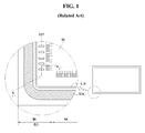
- FIG. 1 is a plane view illustrating the structure of a flat panel liquid crystal display according to related art.
- FIG. 2 is a cross-sectional view illustrating the structure of the liquid crystal display of FIG. 1 by cutting along the line I-I' according to the related art.
- the horizontal electric field type liquid crystal display in which the color filters are formed on the thin film transistor substrate includes a lower panel LP on which are disposed a plurality of pixel areas, each having one thin film transistor and one color filter in a matrix manner, an upper panel UP on which a plurality of black column spacers are disposed between the pixel areas, and a liquid crystal layer LC inserted between the lower panel LP and the upper panel UP.
- the lower panel includes a lower substrate SL made of a transparent material such as the glasses.
- the lower substrate SL has a display area AA occupying at least most of the middle portions for representing the video data, and a non-display area NA surrounding the display area AA.
- the non-display area may also be referred to as the bezel area BZ.
- a plurality of the pixel areas are disposed in a matrix manner.
- a thin film transistor T, a pixel electrode PXL connected to the thin film transistor T, and a color filter CF representing color are allocated in each pixel area.
- the thin film transistor T is disposed at one corner of the pixel area defined in a matrix manner on the lower substrate SL.
- a first passivation layer PAS is deposited on the thin film transistor T for protecting it.
- the color filter CF is formed to cover at least most of the pixel area.
- a red color filter CFR, a green color filter CFG, and a blue color filter CFB may be alternatively disposed on three pixel areas disposed in a serial manner.
- FIG. 2 shows the red and green color filters as examples with the (R) and (G) labels indicated.
- a second passivation layer PAC is deposited on the color filter CF.
- the pixel electrode PXL connecting to the thin film transistor T is formed within the pixel area on the second passivation layer PAC.
- the pixel electrode PXL has a comb structure with a plurality of segments arrayed in parallel. Further, a common electrode COM formed as having a plurality of segments is disposed in parallel with the segments of the pixel electrode PXL one-by-one.
- the upper panel UP includes an upper substrate SU made of a transparent material, such as glass.
- the display area AA and the non-display area NA are defined on one surface of the upper substrate SU, similarly to the lower substrate SL.
- a black column spacer BCS is formed on the whole area of the non-display area NA.
- the black column spacers BCS may be disposed in the display area AA at the area corresponding to the border area between the pixel areas defined on the lower substrate SL.
- the black column spacers BCS are disposed between the color filters CF.
- a gate driver element GIP may be formed in the non-display area NA of the lower panel LP for driving the display element formed in the display area AA. Furthermore, a ground line LIN may be disposed at the outside of the gate driver element GIP.
- the gate driver element GIP has a plurality of thin film transistors. For protecting these thin film transistors of the gate driver element GIP, the black column spacer BCS is usually formed to cover the whole area of the non-display area NA of the upper panel UP.
- the surface of the upper panel UP on which the black column spacers BCS are disposed, and the surface of the lower panel on which the display elements are disposed are joined as facing each other so that the liquid crystal display is completed.
- the column spacer CS maintains an even cell gap between the upper substrate SU and the lower substrate SL. Further, the column spacer CS may provide the black matrix function between the color filters CF, as shown in FIG. 2 .
- the color filter CF is formed on the lower substrate SL with the thin film transistor T as mentioned above, the color filter CF is formed within the pixel areas defined on the lower substrate SL, such that the color filter CF can be just aligned with the pixel area. Further, on the upper panel UP, as only the black column spacer BCS and/or the column spacer CS are formed, the manufacturing process for the upper panel UP may be simplified.
- a sealing material SEAL may be disposed along the circumference along the non-display area NA of the lower panel LP. Further, the liquid crystal layer LC may be disposed within the display area AA of the lower panel LP. After that, the upper panel UP is aligned over the lower panel LP, and then is attached to the lower panel LP. The upper panel UP and the lower panel LP can be bonded to each other by the sealing material SEAL by applying an attaching force, thermal energy, and/or light energy.
- the alignment layers are disposed on each inner upper layer of the lower panel LP and the upper panel UP.
- a lower alignment layer LPI is disposed on the uppermost layer of the lower panel LP.
- An upper alignment layer UPI is disposed on the uppermost layer of the upper panel UP.
- the sealing material SEAL is inserted between the lower alignment layer LPI and the upper alignment layer UPI for adhering the lower panel LP and the upper panel UP.
- the area for disposing the sealing material SEAL must be minimized so that the sealing material SEAL should be disposed on the alignment layers LPI and UPI.
- the sealing material SEAL has a low adhesive property with respect to the alignment layers LPI and UPI, it may cause breaking at the attached portions of the liquid crystal display.
- the sealing material SEAL can be disposed as being apart from the alignment layers LPI and UPI.
- the sealing material SEAL should be disposed on the alignment layers LPI and UPI. Therefore, there is a desire to develop a liquid crystal display having a structure for enhancing the adhesiveness between the sealing material and the alignment layer.
- the present disclosure is directed to a narrow bezel flat panel display that substantially obviates one or more of the problems due to limitations and disadvantages of the related art.
- An object of the present disclosure is to provide a flat panel display having a narrow bezel structure. Another objective of the present disclosure is to provide a narrow bezel structure flat panel display in which the sealing material overlaps with the area for alignment layers, wherein the adhesive property is enhanced between the upper and lower panel. Yet another objective of the present disclosure is to provide an alignment layer that may selectively not cover a portion where the sealing material is disposed.
- the idea of the present invention is to provide a narrow bezel structure flat panel display in which the adhesive property is enhanced between the upper and lower panel by forming at least one trench at an insulating layer where the sealing material is disposed. Since the adhesive strength between the sealing material and the insulating layer, e.g. a planar layer and/or passivation layer, is stronger than that between the sealing material and the alignment layer, an attachment force between the lower and upper panel can be increased.
- a flat panel display including: a lower panel defining a display area and a non-display area, a driver element and a line within the non-display area, a planar layer covering the lower panel, at least one (first) trench at the planar layer over the driver element and the line, a lower alignment layer on an upper surface of the planar layer and a lower surface of the (first) trench, the lower alignment layer exposing a portion of the upper surface of the planar layer at the (first) trench, and a sealant at the (first) trench.
- a flat panel display including: a lower panel defining a display area and a non-display area, a driver element and a line within the non-display area, a planar layer covering the lower panel, at least one trench at the planar layer over the driver element and the line, a passivation layer on an upper surface of the planar layer and the side wall of the trench, a lower alignment layer on an upper surface of the passivation layer and on a lower surface of the trench, the lower alignment layer exposing a portion of the upper surface of the passivation layer at the trench, and a sealant at the first trench.
- a flat panel display including: a panel, a thin film transistor and a line on the panel, an insulating layer covering the thin film transistor and the line, an alignment layer covering the insulating layer, at least one ridge and at least one furrow at the insulating layer on the line, the ridge and the furrow preventing the alignment layer from remaining on the ridge, and a sealant on the alignment layer contacting the insulating layer at the ridge and the furrow.
- a flat panel display comprising: an upper panel and a lower panel having a display area for displaying an image and a non-display area; the lower panel including a first insulating layer and a lower alignment layer disposed on the first insulating layer; at least one trench formed in the insulating layer in the non-display area of the lower panel; wherein the lower alignment layer exposes at least a portion of a side wall of the trench; and a sealant disposed in the non-display area for attaching the lower panel and the upper panel, the sealant filling the trench.
- the non-display area (or bezel area) may surround the display area.
- a liquid crystal layer may be filled between the upper panel and the lower panel, i.e. in the display area.
- the lower alignment layer exposes further at least a portion of the insulating layer adjacent to the trench.
- the exposed portion of the insulating layer is located between two trenches.
- the lower panel includes at least one driver element, e.g. a gate driver element, and at least one line, e.g. a ground line, within the non-display area.
- the sealant may disposed in the non-display area overlapping with the driver element and/or line.
- the at least one trench includes a trench formed overlapping with at least one of the driver element and the line.
- the at least one trench includes a trench formed at a portion of the non-display area between the line and an outer edge of the lower panel.
- the at least one trench includes a first trench formed as a blind hole in the insulating layer with a predetermined depth smaller than a thickness of the insulating layer.
- the trench may penetrate through the insulating layer.
- the lower panel may include a lower substrate and the trench may expose a portion of the lower substrate through the insulating layer.
- the insulating layer includes a planar layer.
- the insulating layer includes a planar layer and a passivation layer on the planar layer.
- the at least one trench includes a trench penetrating through the passivation layer and at least a portion of the planar layer.
- the trench has a tapered shape having a bottom surface (or lower surface) and side walls.
- a taper angle of the trench between at least one of the side walls and the bottom surface is preferably at least 50 degrees. That is, an opening angle in the trench may be defined as an angle adjacent to the taper angle within the trench, the sum of the opening angle and the taper angle being 180 degrees. The opening angle may be obtuse, preferably less than 130 degrees and/or larger than 90 degrees.
- the flat panel display is one of a liquid crystal display, an in-plane switching type liquid crystal display or a fringe-field switching type liquid crystal panel.
- the at least one trench includes a trench extending along a circumference of the lower panel, i.e. a trench surrounding the display area.
- an upper surface of the insulating layer adjacent to the trench has a convex shape.
- the lower surface of the (first) trench is sunk down from the upper surface of the planar layer with a predetermined depth smaller than a thickness of the planar layer.
- the (first) trench may include a side wall connected to the lower surface of the (first) trench.
- the sealant may contact the side wall of the (first) trench and/or an exposed portion of the upper surface of the planar layer or of the passivation layer.
- a taper angle between the side wall and the lower surface may be at least 50 degrees.
- another (second) trench may be provided exposing some of an upper surface of the lower panel at a circumference of the driver element and the line.
- the lower alignment layer exposes a lower surface of the second trench and some upper surface of the planar layer at the second trench.
- the second trench may include a side wall connected to the lower surface of the second trench.
- the sealant may directly contact the exposed upper surface of the planar layer and the side wall.
- FIG. 3 is a plane view illustrating a structure of a flat panel liquid crystal display according to the present disclosure.
- FIG. 4 is a cross-sectional view illustrating a structure of the in-plane switching type flat panel liquid crystal display by cutting along the line II-II' in FIG. 3 according to the present disclosure.
- IPS in-plane switching
- the IPS-type liquid crystal display has a pixel electrode and a common electrode disposed on the same level layer and arrayed in a parallel manner at a predetermined distance from one another.
- One of the main features of the first embodiment is the narrow bezel structure in which the force for attaching the lower panel and the upper panel is enhanced.
- a feature of the liquid crystal display according to the first embodiment is that the sealant SEAL overlaps the gate driver element GIP and the ground line LIN, as shown in FIG. 3 , so that the bezel area BZ is minimized.
- the in-plane switching type liquid crystal display may include a lower panel LP including a plurality of pixel areas, disposed in a matrix manner and having a thin film transistor T and a color filter CF, an upper panel UP having a column spacer CS which may be made of black resin material and disposed between the pixel areas, and a liquid crystal layer LC inserted between the lower panel LP and the upper panel UP.
- the lower panel LP may include a lower substrate SL made of a transparent material, such as glass, and display elements formed on the lower substrate SL.
- the lower substrate SL may have a display area AA occupying the middle portions of the lower substrate SL for representing the video data, and a non-display area NA surrounding the display area AA.
- the non-display area may also be referred to as the bezel area BZ.
- the display area AA a plurality of pixel areas are defined in a matrix manner. In each pixel area, a thin film transistor T, a pixel electrode PXL connected to the thin film transistor T, and a color filter CF for representing color may be allocated.
- the thin film transistor T may be formed at one corner of the pixel area defined on the lower substrate SL.
- a passivation layer PAS may be deposited on the thin film transistor T for protecting the thin film transistor T.
- the color filter CF may be formed as covering at least most of the pixel area on the passivation layer PAS.
- a red color filter CFR, a green color filter CFG and a blue color filter CFB may be alternatively disposed on three pixel areas disposed in a serial manner.
- FIG. 3 shows the red and green color filters as examples with the (R) and (G) labels indicated.
- a planar layer PAC may be deposited on the color filter CF.
- the pixel electrode PXL connecting to the thin film transistor T may be formed within the pixel area on the planar layer PAC.
- the pixel electrode PXL has a comb structure in which a plurality of segments is arrayed in parallel.
- a common electrode COM formed as having a plurality of segments is disposed in parallel with the segments of the pixel electrode PXL, one-by-one.
- a lower alignment layer LPI may be disposed as the uppermost layer of the lower panel LP to cover the whole surface of the lower substrate SL.
- the upper panel UP may include an upper substrate SU made of a transparent material, such as glass.
- the display area AA and the non-display area NA are defined on one surface of the upper substrate SU, similarly to the lower substrate SL.
- a black column spacer BCS may be formed on the whole area of the non-display area NA.
- the column spacers CS may be disposed at the area corresponding to the border area between the pixel areas defined on the lower substrate SL.
- the column spacers CS may be disposed between the color filters CF.
- the black column spacer BCS disposed in the non-display area NA and the column spacer CS disposed in the display area AA may be made of the same material, such as a black resin.
- a gate driver element GIP may be formed in the non-display area NA of the lower panel LP for driving the display element formed in the display area AA. Furthermore, a ground line LIN may be disposed at the outside of the gate driver element GIP.
- the gate driver element GIP may have a plurality of thin film transistors. These thin film transistors may be very sensitive to light incident from outside, e.g., ambient light. For protecting these thin film transistors of the gate driver element GIP from the light, embodiments may include the black column spacer BCS covering the whole area of the non-display area NA of the upper panel UP.
- the surface of the upper panel UP on which the column spacers CS are disposed and the surface of the lower panel on which the display elements are disposed are joined to face each other, with the liquid crystal layer LC in between so that the liquid crystal display is completed.
- the column spacer CS may maintain an even cell gap between the upper substrate SU and the lower substrate SL. Further, the column spacer CS may provide the black matrix function between the color filters CF, as shown in FIG. 4 .
- an upper alignment layer UPI may be disposed as the uppermost layer of the upper panel UP to cover the whole surface of the upper substrate SU. That is, in a flat panel display including the lower panel LP and upper panel UP with the liquid crystal layer LC in between, lower and upper alignment layers LPI and UPI may be disposed in contact with the liquid crystal layer LC.
- the sealant SEAL disposed at the non-display area NA the upper panel UP and the lower panel LP may be attached and/or joined to each other.
- the sealant SEAL preferably overlaps the gate driver element GIP and the ground line LIN. As the result, the bezel area BZ can be minimized.
- the attaching force between the sealant SEAL and the alignment layers LPI and UPI may be remarkably lower than the attaching force between the sealant SEAL and another layer, e.g., the planar layer PAC, or the lower substrate LS. This can cause a problem for attaching or joining the upper panel UP and the lower panel LP.
- embodiments of the present disclosure may include a liquid crystal display having a structure in which the lower alignment layer LPI is partially or selectively not disposed on some area of the lower panel LP where the sealant SEAL is disposed. That is, the lower alignment layer LPI may expose other layers of the lower panel LP.
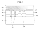
- FIG. 5 is an enlarged cross-sectional view illustrating an attaching structure where the sealant is disposed in FIG. 4 .
- the first trench TR1 has a predetermined depth, which is preferably less than a thickness of the planar layer PAC.
- the first trench TR1 may include a first lower surface LS1, and first side walls SW1 connected to the first lower surface LS1and upper surfaces US1 of the planar layer PAC adjacent to the first trench TR1.
- the first side walls SW1 connect or link the upper surface US1 and the first lower surface LS1 of the first trench TR1.
- the lower alignment layer LPI is not disposed on the upper surfaces US1 of the planar layer PAC next to the first trench TR1. Instead, the lower alignment layer LPI is disposed only on the first lower surface LS1 of the first trench TR1.
- embodiments may include that the first trench TR1 has a tapered shape in direction of the first lower surface LS1.
- a taper angle ( ⁇ ) of the first trench TR1 is at least 50 degrees. That is, the taper or slant angle between the first lower surface LS1 and one of the first side walls SW1 is preferably at least 50 degrees.
- an opening angle of the first trench TR1 formed between the first lower surface LS1 and one of the first side walls SW 1 is preferably an obtuse angle, i.e. preferably more than 90 degrees and less than 130 degrees, the opening angle being defined by the sum of the opening angle and the taper angle being 180 degrees.
- Embodiments may include that the taper angle is larger than 55 degrees.
- the upper surface US1 adjacent to the first trench TR1 may have a convex profile, e.g. the height is slightly lowered from the middle portion to the side portion.
- an upper surface US1 adjacent to the first trench TR1 may be sloped towards the first side wall SW1 of the adjacent first trench TR1.
- a second trench TR2 may be formed in a portion of the planar layer PAC surrounding the gate driver element GIP and the ground line LIN. That is, the ground line LIN may be disposed at the circumference of the lower panel LP and the second trench TR1 may be disposed between an outer edge of the lower panel LP and the ground line LIN.
- the second trench TR2 may be formed to expose the upper surface of the lower substrate SL.
- the second trench TR2 may expose a passivation layer PAS on which the planar layer PAC is formed.
- the second trench TR2 may include a second lower surface LS2 (which is the exposed surface of the lower substrate SL or of the passivation layer PAS), and second side walls SW2 connected to the second lower surface LS2 and upper surfaces US2 of the planar layer PAC adjacent to the second trench TR2, thus linking the upper surfaces US2 next to the second trench TR2and the second lower surface LS2.
- the second trench TR2 may be formed by patterning the planar layer PAC and the passivation layer PAS until exposing the upper surface of the lower substrate SL
- the taper angle of the second trench TR2 is preferably larger than the taper angle ( ⁇ ) of the first trench TR1.
- the upper surface US2 next to the second trench TR2 may also have the convex profile, e.g.
- the height is slightly lowered from the middle portion to the side portion.
- the lower alignment layer LPI may not remain on the second upper surface US2 of the second trench TR2. Most or all of the material of the alignment layer LPI may flow into the second trench TR2.
- upper surfaces US1 or US2 of the planar layer PAC between two of the trenches TR1 or TR2 remain exposed by the alignment layer LPI.
- the lower alignment layer LPI may not be disposed and these portions of planar layer PAC may be exposed.
- the sealant SEAL may directly contact some upper surfaces of the planar layer PAC, especially next to where the trenches are formed.
- the sealant SEAL may directly contact with the side walls of the trenches TR1, TR2.
- FIGs. 6A to 6C are cross-sectional views illustrating a method for manufacturing the thin film transistor substrate for an in-plane switching type liquid crystal display according to the present disclosure.
- a lower substrate SL for the thin film transistor substrate is prepared.
- the thin film transistor T may be formed on the lower substrate SL, and the passivation layer PAS may be deposited to cover the thin film transistor T.
- the color filter CF may be formed within the pixel area on the passivation layer PAS.
- the planar layer PAC may be disposed on the lower substrate SL having the color filter CF to cover the whole surface of the lower substrate SL.
- the drain electrode of the thin film transistor T may be exposed, forming the pixel contact hole at the planar layer PAC.
- the transparent conductive layer IT may be deposited on the planar layer PAC.
- the photoresist PR may be coated on the transparent conductive layer IT.
- the photoresist PR may be patterned to have the same shape of the pixel electrode PXL and the common electrode COM.
- Embodiments may use the half-tone mask for patterning the photoresist PR.
- the half-tone area HT may be defined on the area where the first trench TR1 is formed
- the open area (or "white-tone area") WT may be defined on the area where the second trench TR2 is formed.
- some depth of the second trench TR2 may be patterned at the open area WT. That is, the second trench TR2 may not be fully patterned but may be partially patterned having a predetermined depth. After that, the patterning for etching the remaining depth for the second trench TR2 may be conducted along with patterning the first trench TR1.
- the photoresist PR may be thinned using an ashing process.
- the ashing process may be performed until the photoresist PR on the half-tone area is removed.
- the first trench TR1 may be formed by etching the transparent conductive layer IT and the planar layer PAC exposed by the photoresist PR.
- the remaining depth of the second trench TR2 may be etched to expose the upper surface of the lower substrate SL.
- embodiments may include that the dry etching process is applied. Using the dry etching process, it is possible to ensure that the taper angle of the first trench TR1 is at least 50 degrees.
- the side portions of the planar layer PAC between the trenches may be more etched than the middle portions, so that the upper surface next to the trench has the convex profile, such that the height is slightly lowered from the middle portion to the side portion, as shown in FIG. 6B .
- the transparent conductive layer IT may be patterned to form the pixel electrode PXL and the common electrode COM.
- the transparent conductive layer IT on the non-display area may be removed.
- the lower alignment layer LPI may be disposed on the whole surface of the lower panel LP having the first trench TR1 and the second trench TR2. That is, the lower alignment layer LPI may be disposed on the planar layer PAC.
- the lower alignment layer LPI may not remain on the upper surface of the planar layer PAC next to where the first trench TR1 and the second trench TR2 are located. Instead, the material of the lower alignment layer LPI may flow into the inner space of the first trench TR1 and the second trench TR2, as shown in FIG. 6C .
- the sealant SEAL may directly contact the planar layer PAC. Therefore, it is possible to ensure sufficient attaching or joining force of the sealant SEAL.
- the pixel electrode and the common electrode are disposed in different level layers, and they overlap each other with an insulating layer.
- One of the pixel or common electrodes has the surface type electrode and the other one has a plurality of segments parallel to each other with a predetermined distance.
- the general FFS type liquid crystal display according to the second embodiment of the present disclosure has similarities to the related art, description of similar features may be omitted.
- FIG. 7 is a cross-sectional view illustrating a structure of a fringe field switching type flat panel liquid crystal display by cutting along the line II-II' in FIG. 3 according to the present disclosure.
- the fringe field switching type liquid crystal display may include a lower panel LP including a plurality of pixel areas disposed in a matrix manner and having a thin film transistor T and a color filter CF, an upper panel UP having a column spacer CS disposed between the pixel areas, and a liquid crystal layer LC between the lower panel LP and the upper panel UP.
- the lower panel LP may include a lower substrate SL made of a transparent material, such as glass, and display elements formed on the lower substrate SL.
- the lower substrate SL has a display area AA occupying a middle portion of the lower substrate SL for representing the video data, and a non-display area NA surrounding the display area AA.
- a plurality of pixel areas are defined in a matrix manner.
- a thin film transistor T, a pixel electrode PXL connected to the thin film transistor T, and a color filter CF for representing color are allocated.
- the thin film transistor T may be formed at one corner of the pixel area defined on the lower substrate SL.
- a first passivation layer PAS1 may be deposited on the thin film transistor T for protecting the thin film transistor T.
- the color filter CF may cover at least most of the pixel area on the first passivation layer PAS1.
- a red color filter CFR, a green color filter CFG and a blue color filter CFB may be alternatively disposed on three pixel areas in a serial manner.
- a planar layer PAC is deposited on the color filter CF.
- the common electrode COM having a size and a shape corresponding to those of the color filter CF may be formed within the pixel area on the planar layer PAC. All common electrodes COM disposed in each pixel area may be connected to each other by the common line. Otherwise, the common electrode COM may have a shape covering the whole upper surface of the planar layer PAC, except for some portions, such as the contact holes.
- a second passivation layer PAS2 may be deposited on the whole surface of the lower substrate SL having the common electrode COM.
- the pixel electrode PXL connecting to the thin film transistor T may be formed on the second passivation layer PAS2.
- the pixel electrode PXL has a comb structure with a plurality of segments arrayed in parallel. Further, the segments of the pixel electrode PXL overlap with the common electrode COM on the second passivation layer PAS2.
- a lower alignment layer LPI may be disposed at the uppermost layer of the lower panel LP to cover the whole surface of the lower substrate SL.
- the upper panel UP may include an upper substrate SU made of a transparent material, such as glass.
- the display area AA and the non-display area NA on one surface of the upper substrate SU may be defined like the lower substrate SL.
- a black column spacer BCS may be formed on the whole area of the non-display area NA.
- the column spacers CS may be disposed in the display area AA at the area corresponding to the border area between the pixel areas defined on the lower substrate SL.
- Embodiments may include that the column spacers CS are disposed between the color filters CF.
- the black column spacer BCS disposed in the non-display area NA and the column spacer CS disposed in the display area AA may be made of the same material, such as a black resin material.
- a gate driver element GIP may be formed for driving the display element formed in the display area AA.
- a ground line LIN may be disposed at the outside of the gate driver element GIP.
- the gate driver element GIP may have a plurality of thin film transistors. These thin film transistors may be very sensitive to light incident from outside, e.g., ambient light.
- the black column spacer BCS can be formed to cover the whole area of the non-display area NA of the upper panel UP.
- an upper alignment layer UPI may be disposed at the uppermost layer of the upper panel UP to cover the whole surface of the upper substrate SU.
- the surface of the upper panel UP on which the column spacers CS are disposed and the surface of the lower panel on which the display elements are disposed may be joined to face each other, with the liquid crystal layer LC, so that the liquid crystal display may be completed.
- the column spacer CS may maintain an even cell gap between the upper substrate SU and the lower substrate SL. Further, the column spacer CS may provide the black matrix function between the color filters CF.
- the upper panel UP and the lower panel LP may be attached and/or joined to each other.
- the sealant SEAL may overlap the gate driver element GIP and/or the ground line LIN. As the result, the bezel area BZ can be minimized.
- the attaching force between the sealant SEAL and the alignment layers LPI and UPI may be remarkably lower than the attaching force between the sealant SEAL and another layer, e.g., the planar layer PAC. This can cause a problem for attaching and/or joining the upper panel UP and the lower panel LP.
- the present disclosure provides a liquid crystal display having a structure in which the lower alignment layer LPI is partially or selectively not disposed on some area of the lower panel LP where the sealant SEAL is disposed.
- the portions at which the sealant is disposed in the lower substrate of the FFS type liquid crystal display according to the second embodiment of the present disclosure will be explained.
- FIG. 8 is an enlarged cross-sectional view illustrating an attaching structure where the sealant is disposed in FIG. 7 .
- the trench TR may be formed to penetrate the second passivation layer PAS2 and to sink into the planar layer PAC with a predetermined depth.
- the second trench penetrating the planar layer PAC is not discussed because it was previously described for the first embodiment. However, if required, the second trench may also be formed in the second embodiment.
- the trench TR may have a predetermined depth, preferably less than a sum of the thickness of the second passivation layer PAS2 and the thickness of the planar layer PAC.
- the trench TR may include a lower surface LS, and side walls SW connected to and linking the lower surface LS and an upper surface US of the second passivation layer PAS2 next to the trench TR.
- the lower alignment layer LPI may not remain on the upper surface US next to the trench TR. Instead, the lower alignment layer LPI may be disposed on the lower surface LS.
- embodiments may include that the taper angle ( ⁇ °) of the trench TR is at least 50 degrees. That is, the slant angle between the lower surface LS and the side wall SW is at least 50 degrees. Embodiments may include that the taper angle is larger than 55 degree.
- the lower alignment layer LPI may not remain on the upper surface US of the second passivation layer PAS2. Most or all of the material of the alignment layer LPI may flow into the trench T1.
- upper surfaces US of the second passivation layer PAS2 between two of the trenches TR remain exposed by the alignment layer LPI.
- the lower alignment layer LPI may not be disposed and some upper surfaces of the second passivation layer PAS2 may be exposed.
- the sealant SEAL may directly contact with some upper surfaces of the second passivation layer PAS2, especially next to where the trenches TR are formed.
- the sealant SEAL may directly contact the side walls of the trenches TR. Therefore, the narrow bezel structure according to the present disclosure can provide greater attaching and/or joining forces between the upper panel UP and the lower panel LP than the related art.
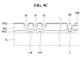
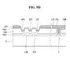
- FIGs. 9A to 9D are cross-sectional views illustrating a method for manufacturing the thin film transistor substrate for a fringe field switching type liquid crystal display according to the present disclosure.
- a lower substrate SL for the thin film transistor substrate is prepared.
- the thin film transistor T may be formed and the first passivation layer PAS1 may be deposited to cover the thin film transistor T.
- the color filter CF may be formed within the pixel area on the passivation layer PAS1.
- the planar layer PAC may be disposed on the lower substrate SL having the color filter CF to cover the whole surface of the lower substrate SL.
- the pixel contact hole PH may be formed by patterning the planar layer PAC.
- the trench TR may be formed, having a predetermined depth, at the planar layer PAC covering the gate driver element GIP and the ground line LIN.
- inventions may use the half-tone mask. Later, by further patterning the first passivation layer PAS1 using the pixel contact hole PH, the pixel contact hole PH may be completed to expose the drain electrode of the thin film transistor T.
- the common electrode COM may be formed on the planar layer PAC having the trench TR and the pixel contact hole PH.
- the second passivation layer PAS2 may be deposited on the whole surface of the lower substrate SL, as shown in FIG. 9B .
- the pixel contact hole PH may be completed to expose the drain electrode of the thin film transistor T.
- the trench TR may be completed.
- the trench TR formed by patterning the planar layer PAC may have a relatively shallow depth, and the side wall SW of the trench TR may have a gentle slope because of the half-tone mask.
- the lower alignment layer LPI may not remain on the upper surface US of the second passivation layer PAS2 adjacent to the trench TR.
- the trench TR may also be etched to complete the trench TR during the process of etching the second passivation layer PAS2 for completing the pixel contact hole PH.
- the transparent conductive layer IT may be deposited on the second passivation layer PAS2, and then the pixel electrode PXL may be formed by patterning the transparent conductive layer IT.
- the lower alignment layer LPI may be disposed on the whole surface of the lower substrate SL having the trench TR and the pixel electrode PXL.
- the lower alignment layer LPI may be disposed on the surface of the second passivation layer PAS2.
- the lower alignment layer LPI may not be disposed on the second passivation layer PAS2 adjacent to where the trenches TR are formed. Instead, the lower alignment layer LPI may flow into the inner space of the trenches TR, as shown in FIG. 9D .
- the sealant SEAL may directly contact the second passivation layer PAS2. Therefore, it is possible to ensure sufficient attaching or joining force of the sealant SEAL.
- the upper panel UP may be attached on the lower panel LP. As such, the liquid crystal display may be complete.
- the first and the second embodiments provide a joining structure for ensuring the enhanced attaching force between those two substrates.
- the alignment layers are not disposed at the area where the sealant is disposed, sufficient attaching or joining force can be ensured.
- the area where the sealant is disposed is the bezel area.
- the bezel area may be too narrow, so that it may be impossible to dispose the alignment layer, except for the sealant area.
- trenches may be formed at the sealant area, so that even though the alignment layers are disposed as covering the bezel area, at least most of the alignment layers may flow into the inner space of the trenches.
- the alignment layers are partially or selectively not disposed at the trench areas.
- the sealant can be attached to other layers having better attaching or joining force than the alignment layers.
- the bezel area includes the gate driver elements and lines, such as a ground line. In that case, it may be preferable that the trenches are formed to not expose or penetrate the passivation layer or planar layer protecting the gate driver elements and lines.
- the taper angle of the side wall of the trench may be less than 30 degrees. In that case, the alignment layers may remain on the upper surface of the trenches. In example embodiments of the present disclosure, the side wall of the trenches may have a taper angle of at least 50 degrees, so that the alignment layers may flow into the trench from the upper surface of the trench.
- example embodiments include that the depth of the trench has a predetermined depth such that the alignment layer may effectively flow into the inner space of the trench.
- the predetermined depth of the trenches There are many possibilities for the predetermined depth of the trenches.
- the second passivation layer is further disposed on the planar layer as in the second embodiment, when the trench is formed at the planar layer and then the second passivation layer is deposited, the taper angle of the side wall of the trenches may be gentle and the depth of the trench may be shallow. In that case, the trench may not work properly. To prevent this problem, some portions of the second passivation layer over the trench may be further etched so that sufficient depth and the taper angle of the trenches can be ensured.
- each trench may be formed next to or over the gate driver elements GIP or the lines, such as the ground line LIN, along the circumference of the substrate.
- Each trench may have a long half-tunnel shape along the lines. Otherwise, a plurality of short trenches may be disposed along the lines. Also, the axes of the plurality of trenches may be perpendicular to the lines.
- the cross-sectional shape of each trench may be the well shape having a profile corresponding to any one of circle, ellipse, rectangular, and so on.
- a ridge and the furrow pattern may be formed at the insulating layer (e.g., "planar layer” and/or “passivation layer”) where the sealant is disposed. That is, more than one trench may be formed in parallel to each other. Thus, a ridge is formed between two trenches, i.e. between two furrows.
- the alignment material may flow into the furrow portions, such that the alignment material may not be disposed on the ridge portions. Then, disposing the sealant where the ridge and the furrow are formed, the sealant may directly contact the ridge portions where the alignment layer is not disposed and the side walls of the trenches or the furrows.
- the sealant may contact other layers than the alignment layer having a worse adhesive property than the other layers.
- the sealant may contact at least one of the insulating layers, such as the planar layer and the passivation layer, and/or the lower substrate having a better adhesive properly than the alignment layer. As a result, it may be possible to ensure a superior adhesive property of the sealant to the substrate.
Landscapes
- Physics & Mathematics (AREA)
- Nonlinear Science (AREA)
- Mathematical Physics (AREA)
- Chemical & Material Sciences (AREA)
- Crystallography & Structural Chemistry (AREA)
- General Physics & Mathematics (AREA)
- Optics & Photonics (AREA)
- Liquid Crystal (AREA)
- Spectroscopy & Molecular Physics (AREA)
- Devices For Indicating Variable Information By Combining Individual Elements (AREA)
Abstract
Description
- This application claims the benefit of
Korean Patent Application No. 10-2014-0154649, filed on November 7, 2014 - The present disclosure relates to a flat panel display with a narrow bezel structure. In particular, the present disclosure relates to a narrow bezel flat panel display in which the area for sealing material (or "sealant") is minimized by enhancing the attaching/adhering force of the sealant disposed between the upper substrate and the lower substrate.
- A liquid crystal display device (LCD) represents video data by controlling the light transitivity of the liquid crystal layer using electric fields. According to the direction of the electric field, the LCD can be classified in two major types: one is a vertical electric field type and the other is a horizontal electric field type.
- For the vertical electric field type LCD, a common electrode formed on an upper substrate and a pixel electrode formed on a lower substrate face each other for forming an electric field perpendicular to the substrate face. A twisted nematic (TN) liquid crystal layer disposed between the upper substrate and the lower substrate is driven by the vertical electric field. The vertical electric field type LCD has a higher aperture ratio than the horizontal electric field type, but it has a narrower view angle of about 90 degrees.
- For the horizontal electric field type LCD, a common electrode and a pixel electrode are formed on the same substrate in parallel. A liquid crystal layer disposed between an upper substrate and a lower substrate is driven in In-Plane-Switching (IPS) mode by an electric field parallel to the substrate face. The horizontal electric field type LCD has a wider view angle of over 170 degrees and a faster response speed than the vertical electric field type LCD. However, the horizontal electric field type LCD may have a lower aperture ratio and transitivity ratio of the back light because there is no electric field over the electrodes, so that the liquid crystals disposed over the electrodes are not driven.
- For most liquid crystal displays, after surface-joining the thin film transistor substrate having a plurality of thin film transistors disposed in a matrix manner and the color filter substrate having a plurality of color filters, the liquid crystal layer is inserted between these surface-joined substrates. Each of the pixel areas defined in the thin film transistor substrate and each of the pixel areas defined in the color filter substrate are correspondingly aligned to each other, as these two substrates are joined. In order to reduce the aligning margin in the joining process, in some cases, the color filters may be formed on the thin film transistor substrate.
-
FIG. 1 is a plane view illustrating the structure of a flat panel liquid crystal display according to related art.FIG. 2 is a cross-sectional view illustrating the structure of the liquid crystal display ofFIG. 1 by cutting along the line I-I' according to the related art. - With reference to
FIGs. 1 and2 , the horizontal electric field type liquid crystal display in which the color filters are formed on the thin film transistor substrate includes a lower panel LP on which are disposed a plurality of pixel areas, each having one thin film transistor and one color filter in a matrix manner, an upper panel UP on which a plurality of black column spacers are disposed between the pixel areas, and a liquid crystal layer LC inserted between the lower panel LP and the upper panel UP. - The lower panel includes a lower substrate SL made of a transparent material such as the glasses. The lower substrate SL has a display area AA occupying at least most of the middle portions for representing the video data, and a non-display area NA surrounding the display area AA. The non-display area may also be referred to as the bezel area BZ. In the display area AA, a plurality of the pixel areas are disposed in a matrix manner. A thin film transistor T, a pixel electrode PXL connected to the thin film transistor T, and a color filter CF representing color are allocated in each pixel area.
- In detail, the thin film transistor T is disposed at one corner of the pixel area defined in a matrix manner on the lower substrate SL. A first passivation layer PAS is deposited on the thin film transistor T for protecting it. On the first passivation layer PAS, the color filter CF is formed to cover at least most of the pixel area. For example, a red color filter CFR, a green color filter CFG, and a blue color filter CFB may be alternatively disposed on three pixel areas disposed in a serial manner.
FIG. 2 shows the red and green color filters as examples with the (R) and (G) labels indicated. - A second passivation layer PAC is deposited on the color filter CF. The pixel electrode PXL connecting to the thin film transistor T is formed within the pixel area on the second passivation layer PAC. For the horizontal electric field type liquid crystal display, the pixel electrode PXL has a comb structure with a plurality of segments arrayed in parallel. Further, a common electrode COM formed as having a plurality of segments is disposed in parallel with the segments of the pixel electrode PXL one-by-one.
- In addition, the upper panel UP includes an upper substrate SU made of a transparent material, such as glass. The display area AA and the non-display area NA are defined on one surface of the upper substrate SU, similarly to the lower substrate SL. A black column spacer BCS is formed on the whole area of the non-display area NA. Further, the black column spacers BCS may be disposed in the display area AA at the area corresponding to the border area between the pixel areas defined on the lower substrate SL. Usually, the black column spacers BCS are disposed between the color filters CF.
- A gate driver element GIP may be formed in the non-display area NA of the lower panel LP for driving the display element formed in the display area AA. Furthermore, a ground line LIN may be disposed at the outside of the gate driver element GIP. The gate driver element GIP has a plurality of thin film transistors. For protecting these thin film transistors of the gate driver element GIP, the black column spacer BCS is usually formed to cover the whole area of the non-display area NA of the upper panel UP.
- After that, with the liquid crystal layer LC, the surface of the upper panel UP on which the black column spacers BCS are disposed, and the surface of the lower panel on which the display elements are disposed are joined as facing each other so that the liquid crystal display is completed. The column spacer CS maintains an even cell gap between the upper substrate SU and the lower substrate SL. Further, the column spacer CS may provide the black matrix function between the color filters CF, as shown in
FIG. 2 . - In the case that the color filter CF is formed on the lower substrate SL with the thin film transistor T as mentioned above, the color filter CF is formed within the pixel areas defined on the lower substrate SL, such that the color filter CF can be just aligned with the pixel area. Further, on the upper panel UP, as only the black column spacer BCS and/or the column spacer CS are formed, the manufacturing process for the upper panel UP may be simplified.
- For example, in order to join the upper panel UP and the lower panel LP, a sealing material SEAL may be disposed along the circumference along the non-display area NA of the lower panel LP. Further, the liquid crystal layer LC may be disposed within the display area AA of the lower panel LP. After that, the upper panel UP is aligned over the lower panel LP, and then is attached to the lower panel LP. The upper panel UP and the lower panel LP can be bonded to each other by the sealing material SEAL by applying an attaching force, thermal energy, and/or light energy.
- For the liquid crystal display, the alignment layers are disposed on each inner upper layer of the lower panel LP and the upper panel UP. A lower alignment layer LPI is disposed on the uppermost layer of the lower panel LP. An upper alignment layer UPI is disposed on the uppermost layer of the upper panel UP. The sealing material SEAL is inserted between the lower alignment layer LPI and the upper alignment layer UPI for adhering the lower panel LP and the upper panel UP.
- In the case that the bezel area BZ is minimized, the area for disposing the sealing material SEAL must be minimized so that the sealing material SEAL should be disposed on the alignment layers LPI and UPI. As the sealing material SEAL has a low adhesive property with respect to the alignment layers LPI and UPI, it may cause breaking at the attached portions of the liquid crystal display. In the cases that the bezel area is relatively wide, the sealing material SEAL can be disposed as being apart from the alignment layers LPI and UPI. However, for the narrow bezel structure, the sealing material SEAL should be disposed on the alignment layers LPI and UPI. Therefore, there is a desire to develop a liquid crystal display having a structure for enhancing the adhesiveness between the sealing material and the alignment layer.
- Accordingly, the present disclosure is directed to a narrow bezel flat panel display that substantially obviates one or more of the problems due to limitations and disadvantages of the related art.
- An object of the present disclosure is to provide a flat panel display having a narrow bezel structure. Another objective of the present disclosure is to provide a narrow bezel structure flat panel display in which the sealing material overlaps with the area for alignment layers, wherein the adhesive property is enhanced between the upper and lower panel. Yet another objective of the present disclosure is to provide an alignment layer that may selectively not cover a portion where the sealing material is disposed. The idea of the present invention is to provide a narrow bezel structure flat panel display in which the adhesive property is enhanced between the upper and lower panel by forming at least one trench at an insulating layer where the sealing material is disposed. Since the adhesive strength between the sealing material and the insulating layer, e.g. a planar layer and/or passivation layer, is stronger than that between the sealing material and the alignment layer, an attachment force between the lower and upper panel can be increased.
- Additional features and advantages will be set forth in the description which follows, and in part will be apparent from the description, or may be learned by practice of the invention. The objectives and other advantages of the invention will be realized and attained by the structure particularly pointed out in the written description and claims hereof as well as the appended drawings.
- The objects are solved by the features of the independent claims. According to one example, there is provided a flat panel display, including: a lower panel defining a display area and a non-display area, a driver element and a line within the non-display area, a planar layer covering the lower panel, at least one (first) trench at the planar layer over the driver element and the line, a lower alignment layer on an upper surface of the planar layer and a lower surface of the (first) trench, the lower alignment layer exposing a portion of the upper surface of the planar layer at the (first) trench, and a sealant at the (first) trench.
- In another example, there is provided a flat panel display, including: a lower panel defining a display area and a non-display area, a driver element and a line within the non-display area, a planar layer covering the lower panel, at least one trench at the planar layer over the driver element and the line, a passivation layer on an upper surface of the planar layer and the side wall of the trench, a lower alignment layer on an upper surface of the passivation layer and on a lower surface of the trench, the lower alignment layer exposing a portion of the upper surface of the passivation layer at the trench, and a sealant at the first trench.
- In another example, there is provided a flat panel display, including: a panel, a thin film transistor and a line on the panel, an insulating layer covering the thin film transistor and the line, an alignment layer covering the insulating layer, at least one ridge and at least one furrow at the insulating layer on the line, the ridge and the furrow preventing the alignment layer from remaining on the ridge, and a sealant on the alignment layer contacting the insulating layer at the ridge and the furrow.
- In another example, there is provided a flat panel display, comprising: an upper panel and a lower panel having a display area for displaying an image and a non-display area; the lower panel including a first insulating layer and a lower alignment layer disposed on the first insulating layer; at least one trench formed in the insulating layer in the non-display area of the lower panel; wherein the lower alignment layer exposes at least a portion of a side wall of the trench; and a sealant disposed in the non-display area for attaching the lower panel and the upper panel, the sealant filling the trench. The non-display area (or bezel area) may surround the display area. A liquid crystal layer may be filled between the upper panel and the lower panel, i.e. in the display area.
- Preferably, for one of these examples, the lower alignment layer exposes further at least a portion of the insulating layer adjacent to the trench. Preferably, the exposed portion of the insulating layer is located between two trenches. Preferably, the lower panel includes at least one driver element, e.g. a gate driver element, and at least one line, e.g. a ground line, within the non-display area. The sealant may disposed in the non-display area overlapping with the driver element and/or line. Preferably, the at least one trench includes a trench formed overlapping with at least one of the driver element and the line. Preferably, the at least one trench includes a trench formed at a portion of the non-display area between the line and an outer edge of the lower panel. Preferably, the at least one trench includes a first trench formed as a blind hole in the insulating layer with a predetermined depth smaller than a thickness of the insulating layer. Also, the trench may penetrate through the insulating layer. For instance, the lower panel may include a lower substrate and the trench may expose a portion of the lower substrate through the insulating layer. Preferably, the insulating layer includes a planar layer. Preferably, the insulating layer includes a planar layer and a passivation layer on the planar layer. Preferably, the at least one trench includes a trench penetrating through the passivation layer and at least a portion of the planar layer. Preferably, the trench has a tapered shape having a bottom surface (or lower surface) and side walls. A taper angle of the trench between at least one of the side walls and the bottom surface is preferably at least 50 degrees. That is, an opening angle in the trench may be defined as an angle adjacent to the taper angle within the trench, the sum of the opening angle and the taper angle being 180 degrees. The opening angle may be obtuse, preferably less than 130 degrees and/or larger than 90 degrees. Preferably, the flat panel display is one of a liquid crystal display, an in-plane switching type liquid crystal display or a fringe-field switching type liquid crystal panel. Preferably, the at least one trench includes a trench extending along a circumference of the lower panel, i.e. a trench surrounding the display area. Preferably, an upper surface of the insulating layer adjacent to the trench has a convex shape.
- Further, preferably, for one of these examples, the lower surface of the (first) trench is sunk down from the upper surface of the planar layer with a predetermined depth smaller than a thickness of the planar layer. The (first) trench may include a side wall connected to the lower surface of the (first) trench. The sealant may contact the side wall of the (first) trench and/or an exposed portion of the upper surface of the planar layer or of the passivation layer. A taper angle between the side wall and the lower surface may be at least 50 degrees. Further, another (second) trench may be provided exposing some of an upper surface of the lower panel at a circumference of the driver element and the line. Preferably, the lower alignment layer exposes a lower surface of the second trench and some upper surface of the planar layer at the second trench. The second trench may include a side wall connected to the lower surface of the second trench. The sealant may directly contact the exposed upper surface of the planar layer and the side wall.
- Other systems, methods, features and advantages will be, or will become, apparent to one with skill in the art upon examination of the following figures and detailed description. It is intended that all such additional systems, methods, features and advantages be included within this description, be within the scope of the present disclosure, and be protected by the following claims. Nothing in this section should be taken as a limitation on those claims. Further aspects and advantages are discussed below in conjunction with the embodiments. It is to be understood that both the foregoing general description and the following detailed description of the present disclosure are examples and explanatory, and are intended to provide further explanation of the disclosure as claimed.
- The accompanying drawings, which are included to provide a further understanding of the invention and are incorporated in and constitute a part of this specification, illustrate implementations of the invention and together with the description serve to explain the principles of the invention.
-
FIG. 1 is a plane view illustrating the structure of a flat panel liquid crystal display according to related art. -
FIG. 2 is a cross-sectional view illustrating the structure of the liquid crystal display ofFIG. 1 by cutting along the line I-I' according to the related art. -
FIG. 3 is a plane view illustrating a structure of a flat panel liquid crystal display according to the present disclosure. -
FIG. 4 is a cross-sectional view illustrating a structure of the in-plane switching type flat panel liquid crystal display by cutting along the line II-II' inFIG. 3 according to the present disclosure. -
FIG. 5 is an enlarged cross-sectional view illustrating an attaching structure where the sealant is disposed inFIG. 4 . -
FIGs. 6A to 6C are cross-sectional views illustrating a method for manufacturing the thin film transistor substrate for an in-plane switching type liquid crystal display according to the present disclosure. -
FIG. 7 is a cross-sectional view illustrating a structure of a fringe field switching type liquid crystal display, one of flat panel display, by cutting along the line II-II' inFIG. 3 according to the present disclosure. -
FIG. 8 is an enlarged cross-sectional view illustrating an attaching structure where the sealant is disposed inFIG. 7 . -
FIGs. 9A to 9D are the cross-sectional views illustrating a method for manufacturing the thin film transistor substrate for a fringe field switching type liquid crystal display according to the present disclosure. - Throughout the drawings and the detailed description, unless otherwise described, the same drawing reference numerals should be understood to refer to the same elements, features, and structures. The relative size and depiction of these elements may be exaggerated for clarity, illustration, and convenience.
- Reference will now be made in detail to embodiments of the present invention, examples of which are illustrated in the accompanying drawings. In the following description, when a detailed description of well-known functions or configurations related to this document is determined to unnecessarily cloud a gist of the invention, the detailed description thereof will be omitted. The progression of processing steps and/or operations described is an example; however, the sequence of steps and/or operations is not limited to that set forth herein and may be changed as is known in the art, with the exception of steps and/or operations necessarily occurring in a certain order. Like reference numerals designate like elements throughout. Names of the respective elements used in the following explanations are selected only for convenience of writing the specification and may be thus different from those used in actual products.
- In the description of embodiments, when a structure is described as being positioned "on or above" or "under or below" another structure, this description should be construed as including a case in which the structures contact each other as well as a case in which a third structure is disposed therebetween.
- A first embodiment of the present disclosure will be explained with reference to
FIGs. 3 and4 .FIG. 3 is a plane view illustrating a structure of a flat panel liquid crystal display according to the present disclosure.FIG. 4 is a cross-sectional view illustrating a structure of the in-plane switching type flat panel liquid crystal display by cutting along the line II-II' inFIG. 3 according to the present disclosure. - For an in-plane switching (IPS) type liquid crystal display, an example of which being a flat panel display according to the first embodiment of the present disclosure, many elements may be very similar to those of the related art. The IPS-type liquid crystal display has a pixel electrode and a common electrode disposed on the same level layer and arrayed in a parallel manner at a predetermined distance from one another. One of the main features of the first embodiment is the narrow bezel structure in which the force for attaching the lower panel and the upper panel is enhanced. For example, in the plane view, a feature of the liquid crystal display according to the first embodiment is that the sealant SEAL overlaps the gate driver element GIP and the ground line LIN, as shown in
FIG. 3 , so that the bezel area BZ is minimized. - In detail, as shown in
FIGs. 3 and4 , the in-plane switching type liquid crystal display according to the first embodiment of the present disclosure may include a lower panel LP including a plurality of pixel areas, disposed in a matrix manner and having a thin film transistor T and a color filter CF, an upper panel UP having a column spacer CS which may be made of black resin material and disposed between the pixel areas, and a liquid crystal layer LC inserted between the lower panel LP and the upper panel UP. - The lower panel LP may include a lower substrate SL made of a transparent material, such as glass, and display elements formed on the lower substrate SL. The lower substrate SL may have a display area AA occupying the middle portions of the lower substrate SL for representing the video data, and a non-display area NA surrounding the display area AA. The non-display area may also be referred to as the bezel area BZ. In the display area AA, a plurality of pixel areas are defined in a matrix manner. In each pixel area, a thin film transistor T, a pixel electrode PXL connected to the thin film transistor T, and a color filter CF for representing color may be allocated.
- The thin film transistor T may be formed at one corner of the pixel area defined on the lower substrate SL. A passivation layer PAS may be deposited on the thin film transistor T for protecting the thin film transistor T. The color filter CF may be formed as covering at least most of the pixel area on the passivation layer PAS. For example, a red color filter CFR, a green color filter CFG and a blue color filter CFB may be alternatively disposed on three pixel areas disposed in a serial manner.
FIG. 3 shows the red and green color filters as examples with the (R) and (G) labels indicated. - A planar layer PAC may be deposited on the color filter CF. The pixel electrode PXL connecting to the thin film transistor T may be formed within the pixel area on the planar layer PAC. For the horizontal electric field type liquid crystal display, the pixel electrode PXL has a comb structure in which a plurality of segments is arrayed in parallel. Further, a common electrode COM formed as having a plurality of segments is disposed in parallel with the segments of the pixel electrode PXL, one-by-one. Furthermore, a lower alignment layer LPI may be disposed as the uppermost layer of the lower panel LP to cover the whole surface of the lower substrate SL.
- In addition, the upper panel UP may include an upper substrate SU made of a transparent material, such as glass. The display area AA and the non-display area NA are defined on one surface of the upper substrate SU, similarly to the lower substrate SL. A black column spacer BCS may be formed on the whole area of the non-display area NA. Further, in the display area AA, the column spacers CS may be disposed at the area corresponding to the border area between the pixel areas defined on the lower substrate SL. In one embodiment, the column spacers CS may be disposed between the color filters CF. The black column spacer BCS disposed in the non-display area NA and the column spacer CS disposed in the display area AA may be made of the same material, such as a black resin.
- A gate driver element GIP may be formed in the non-display area NA of the lower panel LP for driving the display element formed in the display area AA. Furthermore, a ground line LIN may be disposed at the outside of the gate driver element GIP. The gate driver element GIP may have a plurality of thin film transistors. These thin film transistors may be very sensitive to light incident from outside, e.g., ambient light. For protecting these thin film transistors of the gate driver element GIP from the light, embodiments may include the black column spacer BCS covering the whole area of the non-display area NA of the upper panel UP.
- After that, the surface of the upper panel UP on which the column spacers CS are disposed and the surface of the lower panel on which the display elements are disposed are joined to face each other, with the liquid crystal layer LC in between so that the liquid crystal display is completed. The column spacer CS may maintain an even cell gap between the upper substrate SU and the lower substrate SL. Further, the column spacer CS may provide the black matrix function between the color filters CF, as shown in
FIG. 4 . In addition, an upper alignment layer UPI may be disposed as the uppermost layer of the upper panel UP to cover the whole surface of the upper substrate SU. That is, in a flat panel display including the lower panel LP and upper panel UP with the liquid crystal layer LC in between, lower and upper alignment layers LPI and UPI may be disposed in contact with the liquid crystal layer LC. - Using the sealant SEAL disposed at the non-display area NA, the upper panel UP and the lower panel LP may be attached and/or joined to each other. To provide the narrow bezel structure, the sealant SEAL preferably overlaps the gate driver element GIP and the ground line LIN. As the result, the bezel area BZ can be minimized.
- In the case that the sealant SEAL is disposed on the lower and upper alignment layers LPI and UPI, the attaching force between the sealant SEAL and the alignment layers LPI and UPI may be remarkably lower than the attaching force between the sealant SEAL and another layer, e.g., the planar layer PAC, or the lower substrate LS. This can cause a problem for attaching or joining the upper panel UP and the lower panel LP.
- To solve this problem, embodiments of the present disclosure may include a liquid crystal display having a structure in which the lower alignment layer LPI is partially or selectively not disposed on some area of the lower panel LP where the sealant SEAL is disposed. That is, the lower alignment layer LPI may expose other layers of the lower panel LP. Hereinafter, the portions at which the sealant is disposed in the lower substrate of the IPS type liquid crystal display according to the first embodiment of the present disclosure will be explained with reference to
FIGs. 4-5 .FIG. 5 is an enlarged cross-sectional view illustrating an attaching structure where the sealant is disposed inFIG. 4 . - At some portions of the planar layer PAC over the gate driver element GIP and the ground line LIN, at least one first trench TR1 (
FIG. 4 ) may be formed by etching at least some thickness of the planar layer PAC, e.g. by removing at least a part of the planar layer PAC in a portion in the non-display area. - The first trench TR1 has a predetermined depth, which is preferably less than a thickness of the planar layer PAC. The first trench TR1 may include a first lower surface LS1, and first side walls SW1 connected to the first lower surface LS1and upper surfaces US1 of the planar layer PAC adjacent to the first trench TR1. Thus, the first side walls SW1 connect or link the upper surface US1 and the first lower surface LS1 of the first trench TR1. When forming the lower alignment layer LPI on the planar layer PAC having at least one first trench TR1, the lower alignment layer LPI is not disposed on the upper surfaces US1 of the planar layer PAC next to the first trench TR1. Instead, the lower alignment layer LPI is disposed only on the first lower surface LS1 of the first trench TR1.
- In order to not selectively dispose the lower alignment layer LPI on the upper surface US1, embodiments may include that the first trench TR1 has a tapered shape in direction of the first lower surface LS1. A taper angle (θ) of the first trench TR1 is at least 50 degrees. That is, the taper or slant angle between the first lower surface LS1 and one of the first side walls SW1 is preferably at least 50 degrees. Thus, an opening angle of the first trench TR1 formed between the first lower surface LS1 and one of the first
side walls SW 1 is preferably an obtuse angle, i.e. preferably more than 90 degrees and less than 130 degrees, the opening angle being defined by the sum of the opening angle and the taper angle being 180 degrees. Embodiments may include that the taper angle is larger than 55 degrees. Further, the upper surface US1 adjacent to the first trench TR1 may have a convex profile, e.g. the height is slightly lowered from the middle portion to the side portion. In other words, an upper surface US1 adjacent to the first trench TR1 may be sloped towards the first side wall SW1 of the adjacent first trench TR1. With these structures, in forming the lower alignment layer LPI on the lower substrate SL, the lower alignment layer LPI may not remain on the upper surfaces US1 next to the first trench TR1. Most or all of a material of the alignment layer LPI may flow into the first trench TR1. - In addition, in a portion of the planar layer PAC surrounding the gate driver element GIP and the ground line LIN, a second trench TR2 may be formed. That is, the ground line LIN may be disposed at the circumference of the lower panel LP and the second trench TR1 may be disposed between an outer edge of the lower panel LP and the ground line LIN. The second trench TR2 may be formed to expose the upper surface of the lower substrate SL. Alternatively, the second trench TR2 may expose a passivation layer PAS on which the planar layer PAC is formed. For example, the second trench TR2 may include a second lower surface LS2 (which is the exposed surface of the lower substrate SL or of the passivation layer PAS), and second side walls SW2 connected to the second lower surface LS2 and upper surfaces US2 of the planar layer PAC adjacent to the second trench TR2, thus linking the upper surfaces US2 next to the second trench TR2and the second lower surface LS2. As the second trench TR2 may be formed by patterning the planar layer PAC and the passivation layer PAS until exposing the upper surface of the lower substrate SL, the taper angle of the second trench TR2 is preferably larger than the taper angle (θ) of the first trench TR1. Further, the upper surface US2 next to the second trench TR2 may also have the convex profile, e.g. the height is slightly lowered from the middle portion to the side portion. With these structures, in forming the lower alignment layer LPI on the lower substrate SL, the lower alignment layer LPI may not remain on the second upper surface US2 of the second trench TR2. Most or all of the material of the alignment layer LPI may flow into the second trench TR2. In particular, in case of several first or second trenches in parallel (see
Fig. 4 ), upper surfaces US1 or US2 of the planar layer PAC between two of the trenches TR1 or TR2 remain exposed by the alignment layer LPI. - Consequently, on some portions of the planar layer PAC adjacent to the first trench TR1 and/or the second trench TR2, the lower alignment layer LPI may not be disposed and these portions of planar layer PAC may be exposed. As shown in
FIG. 5 , by disposing the sealant SEAL on these structures, the sealant SEAL may directly contact some upper surfaces of the planar layer PAC, especially next to where the trenches are formed. In addition, as the sealant SEAL fills into the trenches, the sealant SEAL may directly contact with the side walls of the trenches TR1, TR2. Hence, not only a contact area for the sealant within the bezel area is increased, but also contact between the sealant and other layers except the alignment layer is provided. Therefore, the narrow bezel structure according to the present disclosure can provide greater attaching and/or joining forces between the upper panel UP and the lower panel LP than the related art. - Hereinafter, the method for manufacturing the thin film transistor substrate for the liquid crystal display according to the first embodiment of the present disclosure will be explained with reference to
FIGs. 6A to 6C. FIGs. 6A to 6C are cross-sectional views illustrating a method for manufacturing the thin film transistor substrate for an in-plane switching type liquid crystal display according to the present disclosure. - As shown in
FIG. 6A , a lower substrate SL for the thin film transistor substrate is prepared. The thin film transistor T may be formed on the lower substrate SL, and the passivation layer PAS may be deposited to cover the thin film transistor T. The color filter CF may be formed within the pixel area on the passivation layer PAS. The planar layer PAC may be disposed on the lower substrate SL having the color filter CF to cover the whole surface of the lower substrate SL. The drain electrode of the thin film transistor T may be exposed, forming the pixel contact hole at the planar layer PAC. The transparent conductive layer IT may be deposited on the planar layer PAC. The photoresist PR may be coated on the transparent conductive layer IT. Using the exposure process and development process, the photoresist PR may be patterned to have the same shape of the pixel electrode PXL and the common electrode COM. Embodiments may use the half-tone mask for patterning the photoresist PR. For example, the half-tone area HT may be defined on the area where the first trench TR1 is formed, and the open area (or "white-tone area") WT may be defined on the area where the second trench TR2 is formed. At first, some depth of the second trench TR2 may be patterned at the open area WT. That is, the second trench TR2 may not be fully patterned but may be partially patterned having a predetermined depth. After that, the patterning for etching the remaining depth for the second trench TR2 may be conducted along with patterning the first trench TR1. - The photoresist PR may be thinned using an ashing process. For example, the ashing process may be performed until the photoresist PR on the half-tone area is removed. After that, using the remaining photoresist PR as the mask, the first trench TR1 may be formed by etching the transparent conductive layer IT and the planar layer PAC exposed by the photoresist PR. At the same time, the remaining depth of the second trench TR2 may be etched to expose the upper surface of the lower substrate SL. For example, embodiments may include that the dry etching process is applied. Using the dry etching process, it is possible to ensure that the taper angle of the first trench TR1 is at least 50 degrees. During the etching process, the side portions of the planar layer PAC between the trenches may be more etched than the middle portions, so that the upper surface next to the trench has the convex profile, such that the height is slightly lowered from the middle portion to the side portion, as shown in
FIG. 6B . - All of the remaining photoresist PR may be removed. Using a further mask process, the transparent conductive layer IT may be patterned to form the pixel electrode PXL and the common electrode COM. By this mask process, the transparent conductive layer IT on the non-display area may be removed. After that, the lower alignment layer LPI may be disposed on the whole surface of the lower panel LP having the first trench TR1 and the second trench TR2. That is, the lower alignment layer LPI may be disposed on the planar layer PAC. However, the lower alignment layer LPI may not remain on the upper surface of the planar layer PAC next to where the first trench TR1 and the second trench TR2 are located. Instead, the material of the lower alignment layer LPI may flow into the inner space of the first trench TR1 and the second trench TR2, as shown in
FIG. 6C . - As the lower alignment layer LPI may not be formed on the planar layer PAC in the area near which the trenches TR1 and/or TR2 are formed, the sealant SEAL may directly contact the planar layer PAC. Therefore, it is possible to ensure sufficient attaching or joining force of the sealant SEAL. After disposing the sealant SEAL on the surface of the non-display area NA where the first trench TR1 and/or the second trench TR2 are formed, and disposing the liquid crystal layer LC within the display area AA, the upper panel UP may be attached on the lower panel LP. As such, the liquid crystal display may be complete.
- In the first embodiment above, a structure for enhancing the joining and/or attaching force in the in-plane switching type liquid crystal display was explained. Hereinafter, a structure for enhancing the joining/attaching force in the fringe field switching (FFS) type liquid crystal display will be explained. For the FFS type, as the common electrode and the pixel electrode are disposed in different level layers, the cross-sectional structure is more complicated than that of the IPS type.
- In the second embodiment, the detailed structure applied with the idea of the present disclosure to the FFS type liquid crystal display will be explained. One feature of the FFS type is that the pixel electrode and the common electrode are disposed in different level layers, and they overlap each other with an insulating layer. One of the pixel or common electrodes has the surface type electrode and the other one has a plurality of segments parallel to each other with a predetermined distance. As the general FFS type liquid crystal display according to the second embodiment of the present disclosure has similarities to the related art, description of similar features may be omitted.
- Further, as one of the features in the second embodiment is at the non-display area NA, there will also be reference to
FIG. 3 , which is an example of the first embodiment.FIG. 7 is a cross-sectional view illustrating a structure of a fringe field switching type flat panel liquid crystal display by cutting along the line II-II' inFIG. 3 according to the present disclosure. - The fringe field switching type liquid crystal display according to the second embodiment of the present disclosure may include a lower panel LP including a plurality of pixel areas disposed in a matrix manner and having a thin film transistor T and a color filter CF, an upper panel UP having a column spacer CS disposed between the pixel areas, and a liquid crystal layer LC between the lower panel LP and the upper panel UP.
- The lower panel LP may include a lower substrate SL made of a transparent material, such as glass, and display elements formed on the lower substrate SL. The lower substrate SL has a display area AA occupying a middle portion of the lower substrate SL for representing the video data, and a non-display area NA surrounding the display area AA. In the display area AA, a plurality of pixel areas are defined in a matrix manner. In each pixel area, a thin film transistor T, a pixel electrode PXL connected to the thin film transistor T, and a color filter CF for representing color are allocated.
- The thin film transistor T may be formed at one corner of the pixel area defined on the lower substrate SL. A first passivation layer PAS1 may be deposited on the thin film transistor T for protecting the thin film transistor T. The color filter CF may cover at least most of the pixel area on the first passivation layer PAS1. For example, a red color filter CFR, a green color filter CFG and a blue color filter CFB may be alternatively disposed on three pixel areas in a serial manner.
- A planar layer PAC is deposited on the color filter CF. The common electrode COM having a size and a shape corresponding to those of the color filter CF may be formed within the pixel area on the planar layer PAC. All common electrodes COM disposed in each pixel area may be connected to each other by the common line. Otherwise, the common electrode COM may have a shape covering the whole upper surface of the planar layer PAC, except for some portions, such as the contact holes.
- A second passivation layer PAS2 may be deposited on the whole surface of the lower substrate SL having the common electrode COM. The pixel electrode PXL connecting to the thin film transistor T may be formed on the second passivation layer PAS2. For the FFS type liquid crystal display, the pixel electrode PXL has a comb structure with a plurality of segments arrayed in parallel. Further, the segments of the pixel electrode PXL overlap with the common electrode COM on the second passivation layer PAS2. Further, a lower alignment layer LPI may be disposed at the uppermost layer of the lower panel LP to cover the whole surface of the lower substrate SL.
- In addition, the upper panel UP may include an upper substrate SU made of a transparent material, such as glass. The display area AA and the non-display area NA on one surface of the upper substrate SU may be defined like the lower substrate SL. A black column spacer BCS may be formed on the whole area of the non-display area NA. Further, the column spacers CS may be disposed in the display area AA at the area corresponding to the border area between the pixel areas defined on the lower substrate SL. Embodiments may include that the column spacers CS are disposed between the color filters CF. The black column spacer BCS disposed in the non-display area NA and the column spacer CS disposed in the display area AA may be made of the same material, such as a black resin material.
- In the non-display area NA of the lower panel LP, a gate driver element GIP may be formed for driving the display element formed in the display area AA. Further, a ground line LIN may be disposed at the outside of the gate driver element GIP. The gate driver element GIP may have a plurality of thin film transistors. These thin film transistors may be very sensitive to light incident from outside, e.g., ambient light. For protecting these thin film transistors of the gate driver element GIP from the light, the black column spacer BCS can be formed to cover the whole area of the non-display area NA of the upper panel UP. Further, an upper alignment layer UPI may be disposed at the uppermost layer of the upper panel UP to cover the whole surface of the upper substrate SU.
- After that, the surface of the upper panel UP on which the column spacers CS are disposed and the surface of the lower panel on which the display elements are disposed may be joined to face each other, with the liquid crystal layer LC, so that the liquid crystal display may be completed. The column spacer CS may maintain an even cell gap between the upper substrate SU and the lower substrate SL. Further, the column spacer CS may provide the black matrix function between the color filters CF.
- Using the sealant SEAL disposed at the non-display area NA, the upper panel UP and the lower panel LP may be attached and/or joined to each other. For example, in order to provide the narrow bezel structure, the sealant SEAL may overlap the gate driver element GIP and/or the ground line LIN. As the result, the bezel area BZ can be minimized.
- In the case that the sealant SEAL is disposed on the lower and upper alignment layers LPI and UPI, the attaching force between the sealant SEAL and the alignment layers LPI and UPI may be remarkably lower than the attaching force between the sealant SEAL and another layer, e.g., the planar layer PAC. This can cause a problem for attaching and/or joining the upper panel UP and the lower panel LP.
- To solve this problem, the present disclosure provides a liquid crystal display having a structure in which the lower alignment layer LPI is partially or selectively not disposed on some area of the lower panel LP where the sealant SEAL is disposed. Hereinafter, with reference to
FIGs. 7-8 , the portions at which the sealant is disposed in the lower substrate of the FFS type liquid crystal display according to the second embodiment of the present disclosure will be explained.FIG. 8 is an enlarged cross-sectional view illustrating an attaching structure where the sealant is disposed inFIG. 7 . - At some portions of the second passivation layer PAS2 and the planar layer PAC over or next to the gate driver element GIP and the ground line LIN, at least one trench TR may be formed, e.g. by etching the second passivation layer PAS2 to expose the planar layer PAC, and preferably also some thickness of the planar layer PAC. For example, in the second embodiment, the trench TR may be formed to penetrate the second passivation layer PAS2 and to sink into the planar layer PAC with a predetermined depth. For convenience, in the second embodiment, the second trench penetrating the planar layer PAC is not discussed because it was previously described for the first embodiment. However, if required, the second trench may also be formed in the second embodiment.
- The trench TR may have a predetermined depth, preferably less than a sum of the thickness of the second passivation layer PAS2 and the thickness of the planar layer PAC. The trench TR may include a lower surface LS, and side walls SW connected to and linking the lower surface LS and an upper surface US of the second passivation layer PAS2 next to the trench TR. In forming the lower alignment layer LPI on the second passivation layer PAS2 and the planar layer PAC having the trench TR, the lower alignment layer LPI may not remain on the upper surface US next to the trench TR. Instead, the lower alignment layer LPI may be disposed on the lower surface LS.
- In order to not selectively dispose the lower alignment layer LPI on the upper surface US, embodiments may include that the taper angle (θ°) of the trench TR is at least 50 degrees. That is, the slant angle between the lower surface LS and the side wall SW is at least 50 degrees. Embodiments may include that the taper angle is larger than 55 degree. With these structures, in forming the lower alignment layer LPI on the lower substrate SL, the lower alignment layer LPI may not remain on the upper surface US of the second passivation layer PAS2. Most or all of the material of the alignment layer LPI may flow into the trench T1. In particular, in case of several (first or second) trenches TR in parallel (see
Fig. 7 or8 ), upper surfaces US of the second passivation layer PAS2 between two of the trenches TR remain exposed by the alignment layer LPI. - Consequently, on some portions of the second passivation layer PAS2 and the planar layer PAC where the trench TR is formed, the lower alignment layer LPI may not be disposed and some upper surfaces of the second passivation layer PAS2 may be exposed. As shown in
FIG. 8 , by disposing the sealant SEAL on these structures, the sealant SEAL may directly contact with some upper surfaces of the second passivation layer PAS2, especially next to where the trenches TR are formed. In addition, as the sealant SEAL fills into the inner spaces of the trenches TR, the sealant SEAL may directly contact the side walls of the trenches TR. Therefore, the narrow bezel structure according to the present disclosure can provide greater attaching and/or joining forces between the upper panel UP and the lower panel LP than the related art. - Hereinafter, with reference to
FIGs. 9A to 9D , the method for manufacturing the thin film transistor substrate for the liquid crystal display according to the second embodiment of the present disclosure will be explained.FIGs. 9A to 9D are cross-sectional views illustrating a method for manufacturing the thin film transistor substrate for a fringe field switching type liquid crystal display according to the present disclosure. - As shown in
FIG. 9A , a lower substrate SL for the thin film transistor substrate is prepared. On the lower substrate SL, the thin film transistor T may be formed and the first passivation layer PAS1 may be deposited to cover the thin film transistor T. The color filter CF may be formed within the pixel area on the passivation layer PAS1. The planar layer PAC may be disposed on the lower substrate SL having the color filter CF to cover the whole surface of the lower substrate SL. The pixel contact hole PH may be formed by patterning the planar layer PAC. The trench TR may be formed, having a predetermined depth, at the planar layer PAC covering the gate driver element GIP and the ground line LIN. The depth of the trench TR and the depth of the pixel contact hole PH are different from each other. Therefore, embodiments may use the half-tone mask. Later, by further patterning the first passivation layer PAS1 using the pixel contact hole PH, the pixel contact hole PH may be completed to expose the drain electrode of the thin film transistor T. - The common electrode COM may be formed on the planar layer PAC having the trench TR and the pixel contact hole PH. The second passivation layer PAS2 may be deposited on the whole surface of the lower substrate SL, as shown in
FIG. 9B . - By patterning the second passivation layer PAS2 and the first passivation layer PAS1, the pixel contact hole PH may be completed to expose the drain electrode of the thin film transistor T. Here, by etching the second passivation layer PAS2 and some depth of the planar layer PAC, the trench TR may be completed. The trench TR formed by patterning the planar layer PAC may have a relatively shallow depth, and the side wall SW of the trench TR may have a gentle slope because of the half-tone mask. When disposing the lower alignment layer LPI under this structure, the lower alignment layer LPI may not remain on the upper surface US of the second passivation layer PAS2 adjacent to the trench TR. In order that the trench TR has sufficient depth and taper angle, the trench TR may also be etched to complete the trench TR during the process of etching the second passivation layer PAS2 for completing the pixel contact hole PH.
- The transparent conductive layer IT may be deposited on the second passivation layer PAS2, and then the pixel electrode PXL may be formed by patterning the transparent conductive layer IT. After that, the lower alignment layer LPI may be disposed on the whole surface of the lower substrate SL having the trench TR and the pixel electrode PXL. As the result, the lower alignment layer LPI may be disposed on the surface of the second passivation layer PAS2. However, the lower alignment layer LPI may not be disposed on the second passivation layer PAS2 adjacent to where the trenches TR are formed. Instead, the lower alignment layer LPI may flow into the inner space of the trenches TR, as shown in
FIG. 9D . - As the lower alignment layer LPI may not be disposed on the second passivation layer PAS2 in the area in which the trenches are formed, the sealant SEAL may directly contact the second passivation layer PAS2. Therefore, it is possible to ensure sufficient attaching or joining force of the sealant SEAL. After disposing the sealant SEAL on the surface of the non-display area NA where the trenches TR are formed, and disposing the liquid crystal layer LC within the display area AA, the upper panel UP may be attached on the lower panel LP. As such, the liquid crystal display may be complete.
- In the flat panel display in which the alignment layers are disposed as the uppermost layers and two substrates are joined to form the flat panel display according to the present disclosure, the first and the second embodiments provide a joining structure for ensuring the enhanced attaching force between those two substrates. In a case in which the alignment layers are not disposed at the area where the sealant is disposed, sufficient attaching or joining force can be ensured. The area where the sealant is disposed is the bezel area. For the narrow bezel structure, the bezel area may be too narrow, so that it may be impossible to dispose the alignment layer, except for the sealant area.
- According to embodiments of the present disclosure, trenches may be formed at the sealant area, so that even though the alignment layers are disposed as covering the bezel area, at least most of the alignment layers may flow into the inner space of the trenches. The alignment layers are partially or selectively not disposed at the trench areas. The sealant can be attached to other layers having better attaching or joining force than the alignment layers. Especially, for the narrow bezel structure, the bezel area includes the gate driver elements and lines, such as a ground line. In that case, it may be preferable that the trenches are formed to not expose or penetrate the passivation layer or planar layer protecting the gate driver elements and lines.
- In a case in which the trenches are formed as the passivation layer and/or the planar layer are not penetrated, the taper angle of the side wall of the trench may be less than 30 degrees. In that case, the alignment layers may remain on the upper surface of the trenches. In example embodiments of the present disclosure, the side wall of the trenches may have a taper angle of at least 50 degrees, so that the alignment layers may flow into the trench from the upper surface of the trench.
- Further, example embodiments include that the depth of the trench has a predetermined depth such that the alignment layer may effectively flow into the inner space of the trench. There are many possibilities for the predetermined depth of the trenches. In a case in which the second passivation layer is further disposed on the planar layer as in the second embodiment, when the trench is formed at the planar layer and then the second passivation layer is deposited, the taper angle of the side wall of the trenches may be gentle and the depth of the trench may be shallow. In that case, the trench may not work properly. To prevent this problem, some portions of the second passivation layer over the trench may be further etched so that sufficient depth and the taper angle of the trenches can be ensured.
- In addition, each trench may be formed next to or over the gate driver elements GIP or the lines, such as the ground line LIN, along the circumference of the substrate. Each trench may have a long half-tunnel shape along the lines. Otherwise, a plurality of short trenches may be disposed along the lines. Also, the axes of the plurality of trenches may be perpendicular to the lines. The cross-sectional shape of each trench may be the well shape having a profile corresponding to any one of circle, ellipse, rectangular, and so on.
- In another example embodiment of the present disclosure, a ridge and the furrow pattern may be formed at the insulating layer (e.g., "planar layer" and/or "passivation layer") where the sealant is disposed. That is, more than one trench may be formed in parallel to each other. Thus, a ridge is formed between two trenches, i.e. between two furrows. In forming the alignment layer on the insulating layer, the alignment material may flow into the furrow portions, such that the alignment material may not be disposed on the ridge portions. Then, disposing the sealant where the ridge and the furrow are formed, the sealant may directly contact the ridge portions where the alignment layer is not disposed and the side walls of the trenches or the furrows. That is, the sealant may contact other layers than the alignment layer having a worse adhesive property than the other layers. For instance, the sealant may contact at least one of the insulating layers, such as the planar layer and the passivation layer, and/or the lower substrate having a better adhesive properly than the alignment layer. As a result, it may be possible to ensure a superior adhesive property of the sealant to the substrate.
- It will be apparent to those skilled in the art that various modifications and variations can be made in the present invention without departing from the scope of the invention. Thus, it is intended that embodiments of the present invention cover the modifications and variations of this invention provided they come within the scope of the appended claims and their equivalents.
Claims (15)
- A flat panel display, comprising:an upper panel and a lower panel having a display area for displaying an image and a non-display area;the lower panel including a first insulating layer and a lower alignment layer disposed on the first insulating layer;at least one trench formed in the insulating layer in the non-display area of the lower panel;wherein the lower alignment layer exposes at least a portion of a side wall of the trench; anda sealant disposed in the non-display area for attaching the lower panel and the upper panel, the sealant filling the trench.
- The flat panel display of claim 1, wherein the lower alignment layer exposes further at least a portion of the insulating layer adjacent to the trench.
- The flat panel display of claim 2, wherein the exposed portion of the insulating layer is located between two trenches.
- The flat panel display according to any one of the preceding claims, wherein the lower panel includes at least one driver element and at least one line within the non-display area.
- The flat panel display of claim 4, wherein the at least one trench includes a trench formed overlapping with at least one of the driver element and the line.
- The flat panel display of claim 4 or 5, wherein the at least one trench includes a trench formed at a portion of the non-display area between the line and an outer edge of the lower panel.
- The flat panel display according to any one of the preceding claims, wherein the at least one trench includes a first trench formed as a blind hole in the insulating layer with a predetermined depth smaller than a thickness of the insulating layer.
- The flat panel display according to any one of the preceding claims, wherein the lower panel includes a lower substrate and the at least one trench includes a second trench exposing a portion of the lower substrate.
- The flat panel display according to any one of the preceding claims, wherein the insulating layer includes a planar layer.
- The flat panel display according to any one of the preceding claims, wherein the insulating layer includes a planar layer and a passivation layer on the planar layer.
- The flat panel display of claim 10, wherein the at least one trench includes a trench penetrating through the passivation layer and at least a portion of the planar layer.
- The flat panel display according to any one of the preceding claims, wherein the trench has a tapered shape having a bottom surface and side walls, and a taper angle between the side wall and the bottom surface in the trench is at least 50 degrees.
- The flat panel display according to any one of the preceding claims, wherein the flat panel display is one of a liquid crystal display, an in-plane switching type liquid crystal display or a fringe-field switching type liquid crystal panel.
- The flat panel display according to any one of the preceding claims, wherein the at least one trench includes a trench extending along a circumference of the lower panel.
- The flat panel display according to any one of the preceding claims, wherein an upper surface of the insulating layer adjacent to the trench has a convex shape.
Applications Claiming Priority (1)
| Application Number | Priority Date | Filing Date | Title |
|---|---|---|---|
| KR1020140154649A KR102045034B1 (en) | 2014-11-07 | 2014-11-07 | Narrow Bezel Flat Panel Display |
Publications (2)
| Publication Number | Publication Date |
|---|---|
| EP3018525A1 true EP3018525A1 (en) | 2016-05-11 |
| EP3018525B1 EP3018525B1 (en) | 2018-04-25 |
Family
ID=54476854
Family Applications (1)
| Application Number | Title | Priority Date | Filing Date |
|---|---|---|---|
| EP15193460.1A Active EP3018525B1 (en) | 2014-11-07 | 2015-11-06 | Narrow bezel flat panel display |
Country Status (4)
| Country | Link |
|---|---|
| US (1) | US9570478B2 (en) |
| EP (1) | EP3018525B1 (en) |
| KR (1) | KR102045034B1 (en) |
| CN (1) | CN105589264B (en) |
Cited By (2)
| Publication number | Priority date | Publication date | Assignee | Title |
|---|---|---|---|---|
| EP3812832A1 (en) * | 2019-10-23 | 2021-04-28 | InnoLux Corporation | Electronic device |
| TWI730903B (en) * | 2020-09-23 | 2021-06-11 | 友達光電股份有限公司 | Display panel |
Families Citing this family (24)
| Publication number | Priority date | Publication date | Assignee | Title |
|---|---|---|---|---|
| CN105137665A (en) * | 2015-09-30 | 2015-12-09 | 京东方科技集团股份有限公司 | Display substrate, preparation method thereof, and display device |
| JP6616897B2 (en) * | 2016-06-28 | 2019-12-04 | シャープ株式会社 | Display panel |
| KR102597230B1 (en) * | 2016-10-31 | 2023-11-01 | 엘지디스플레이 주식회사 | Liquid crystal display panel |
| KR102773125B1 (en) * | 2016-11-09 | 2025-02-26 | 삼성디스플레이 주식회사 | Liquid crystal display device |
| US11079886B2 (en) * | 2017-03-10 | 2021-08-03 | Sharp Kabushiki Kaisha | Display substrate and display device |
| US11150502B2 (en) * | 2017-03-10 | 2021-10-19 | Sharp Kabushiki Kaisha | Display substrate and display device |
| JP2018185473A (en) * | 2017-04-27 | 2018-11-22 | 株式会社ジャパンディスプレイ | Display device |
| CN106918954A (en) * | 2017-05-10 | 2017-07-04 | 京东方科技集团股份有限公司 | A kind of orientation membrane preparation method, display base plate and display panel |
| WO2019004051A1 (en) * | 2017-06-28 | 2019-01-03 | シャープ株式会社 | Display device substrate and display device |
| JP2019078789A (en) * | 2017-10-20 | 2019-05-23 | シャープ株式会社 | Substrate for display device and display device |
| CN109830181A (en) * | 2017-11-23 | 2019-05-31 | 群创光电股份有限公司 | Display device |
| CN109407411A (en) * | 2018-11-20 | 2019-03-01 | 深圳市华星光电技术有限公司 | Alignment film coating method and liquid crystal display panel |
| TWI683159B (en) * | 2018-11-20 | 2020-01-21 | 友達光電股份有限公司 | Display panel |
| CN111308752B (en) | 2018-12-11 | 2023-04-07 | 群创光电股份有限公司 | Display device |
| WO2021072675A1 (en) * | 2019-10-16 | 2021-04-22 | Boe Technology Group Co., Ltd. | Method of encapsulating display substrate and counter substrate, encapsulated display panel, display apparatus, and counter substrate |
| CN110967877A (en) * | 2019-12-20 | 2020-04-07 | Tcl华星光电技术有限公司 | Display panel |
| CN113568225A (en) * | 2021-07-09 | 2021-10-29 | 西安中科微星光电科技有限公司 | Liquid crystal light valve module packaging structure |
| CN113867025B (en) * | 2021-09-23 | 2024-01-23 | 武汉华星光电技术有限公司 | Display panel and mobile terminal |
| CN114227018B (en) * | 2022-01-11 | 2026-03-17 | 福建华佳彩有限公司 | A structure and method for efficient cutting of display panels suitable for irregularly shaped screens |
| CN116719191A (en) * | 2022-01-25 | 2023-09-08 | 厦门天马微电子有限公司 | Array substrate and display panel |
| CN114994988B (en) | 2022-05-30 | 2023-08-08 | 合肥鑫晟光电科技有限公司 | Display substrate and display device |
| CN115561935A (en) * | 2022-09-05 | 2023-01-03 | 武汉华星光电技术有限公司 | Display panel and display device |
| KR20240065840A (en) * | 2022-11-07 | 2024-05-14 | 삼성전자주식회사 | Semiconductor package |
| CN116613178A (en) * | 2023-06-30 | 2023-08-18 | 天马新型显示技术研究院(厦门)有限公司 | Display panel and display device |
Citations (2)
| Publication number | Priority date | Publication date | Assignee | Title |
|---|---|---|---|---|
| WO2013175709A1 (en) * | 2012-05-25 | 2013-11-28 | シャープ株式会社 | Liquid crystal display device |
| US20140320789A1 (en) * | 2013-04-29 | 2014-10-30 | Lg Display Co., Ltd. | Liquid crystal display device and manufacturing method thereof |
Family Cites Families (9)
| Publication number | Priority date | Publication date | Assignee | Title |
|---|---|---|---|---|
| JP2002341357A (en) * | 2001-05-14 | 2002-11-27 | Matsushita Electric Ind Co Ltd | Manufacturing method and manufacturing apparatus for liquid crystal display device |
| KR100865284B1 (en) * | 2001-10-31 | 2008-10-27 | 엘지디스플레이 주식회사 | Sealing structure of liquid crystal panel |
| US7538488B2 (en) * | 2004-02-14 | 2009-05-26 | Samsung Mobile Display Co., Ltd. | Flat panel display |
| KR101100892B1 (en) * | 2004-08-27 | 2012-01-02 | 삼성전자주식회사 | Display device |
| KR101073404B1 (en) * | 2008-06-25 | 2011-10-17 | 엘지디스플레이 주식회사 | Liquid crystal display panel and method of fabricating the same |
| JP2010091896A (en) * | 2008-10-10 | 2010-04-22 | Hitachi Displays Ltd | Liquid crystal display device |
| TWI471661B (en) * | 2011-06-29 | 2015-02-01 | Innolux Corp | System for display images |
| KR101848827B1 (en) * | 2011-08-04 | 2018-04-17 | 엘지디스플레이 주식회사 | Liquid crystal display device |
| KR102126381B1 (en) * | 2013-10-14 | 2020-06-25 | 삼성디스플레이 주식회사 | Display apparutus |
-
2014
- 2014-11-07 KR KR1020140154649A patent/KR102045034B1/en active Active
-
2015
- 2015-11-06 EP EP15193460.1A patent/EP3018525B1/en active Active
- 2015-11-06 US US14/934,242 patent/US9570478B2/en active Active
- 2015-11-09 CN CN201510754089.5A patent/CN105589264B/en active Active
Patent Citations (2)
| Publication number | Priority date | Publication date | Assignee | Title |
|---|---|---|---|---|
| WO2013175709A1 (en) * | 2012-05-25 | 2013-11-28 | シャープ株式会社 | Liquid crystal display device |
| US20140320789A1 (en) * | 2013-04-29 | 2014-10-30 | Lg Display Co., Ltd. | Liquid crystal display device and manufacturing method thereof |
Cited By (3)
| Publication number | Priority date | Publication date | Assignee | Title |
|---|---|---|---|---|
| EP3812832A1 (en) * | 2019-10-23 | 2021-04-28 | InnoLux Corporation | Electronic device |
| US11347113B2 (en) | 2019-10-23 | 2022-05-31 | Innolux Corporation | Electronic device |
| TWI730903B (en) * | 2020-09-23 | 2021-06-11 | 友達光電股份有限公司 | Display panel |
Also Published As
| Publication number | Publication date |
|---|---|
| US20160133653A1 (en) | 2016-05-12 |
| EP3018525B1 (en) | 2018-04-25 |
| US9570478B2 (en) | 2017-02-14 |
| CN105589264A (en) | 2016-05-18 |
| KR102045034B1 (en) | 2019-11-15 |
| KR20160055353A (en) | 2016-05-18 |
| CN105589264B (en) | 2019-03-08 |
Similar Documents
| Publication | Publication Date | Title |
|---|---|---|
| EP3018525B1 (en) | Narrow bezel flat panel display | |
| KR101192770B1 (en) | Liquid Crystal Display Panel and Method of Fabricating the same | |
| KR101984269B1 (en) | Liquid crystal display device and manufacturing method thereof | |
| CN103543561B (en) | Liquid crystal display device | |
| CN105404059B (en) | Liquid crystal display device and motherboard | |
| KR102672348B1 (en) | Narrow bezel display device | |
| JP5080435B2 (en) | Array substrate for liquid crystal display device and manufacturing method thereof | |
| US10197842B2 (en) | Liquid crystal display device | |
| CN103676333A (en) | Color filter substrate and liquid crystal display device including same | |
| CN102073181B (en) | Display base plate, its manufacture method and there is the display device of this display base plate | |
| CN110867453B (en) | Semiconductor device, display device, and method for manufacturing semiconductor device | |
| US20100014043A1 (en) | Liquid crystal display element | |
| KR102112093B1 (en) | Narrow Bezel Flat Panel Display | |
| KR20050001942A (en) | Mother glass substrate for liquid crystal display device | |
| CN110308596B (en) | Display device | |
| EP3316033B1 (en) | Thin film transistor substrate having color filter | |
| KR20160010114A (en) | Display device and manufacturing method of the same | |
| KR20130027189A (en) | Liquid crystal display and method for manufacturing the same | |
| KR102420997B1 (en) | Display device | |
| CN107367860B (en) | LCD assembly | |
| KR20150084566A (en) | Display apparatus and fabrication method thereof | |
| KR20180062572A (en) | Narrow bezel panel display | |
| KR102263995B1 (en) | Substrate for liquid crystal display panel, manufacturing method thereof, liquid crystal display panel comprising the same | |
| KR102168718B1 (en) | Narrow Bezel Flat Panel Display | |
| WO2012144433A1 (en) | Method for manufacturing display device, method for manufacturing liquid crystal display device, and liquid crystal display device |
Legal Events
| Date | Code | Title | Description |
|---|---|---|---|
| PUAI | Public reference made under article 153(3) epc to a published international application that has entered the european phase |
Free format text: ORIGINAL CODE: 0009012 |
|
| AK | Designated contracting states |
Kind code of ref document: A1 Designated state(s): AL AT BE BG CH CY CZ DE DK EE ES FI FR GB GR HR HU IE IS IT LI LT LU LV MC MK MT NL NO PL PT RO RS SE SI SK SM TR |
|
| AX | Request for extension of the european patent |
Extension state: BA ME |
|
| 17P | Request for examination filed |
Effective date: 20160727 |
|
| RBV | Designated contracting states (corrected) |
Designated state(s): AL AT BE BG CH CY CZ DE DK EE ES FI FR GB GR HR HU IE IS IT LI LT LU LV MC MK MT NL NO PL PT RO RS SE SI SK SM TR |
|
| 17Q | First examination report despatched |
Effective date: 20161222 |
|
| RIC1 | Information provided on ipc code assigned before grant |
Ipc: G02F 1/1345 20060101ALI20170808BHEP Ipc: G02F 1/1333 20060101ALN20170808BHEP Ipc: G02F 1/1339 20060101AFI20170808BHEP |
|
| RIC1 | Information provided on ipc code assigned before grant |
Ipc: G02F 1/1339 20060101AFI20170811BHEP Ipc: G02F 1/1345 20060101ALI20170811BHEP Ipc: G02F 1/1333 20060101ALN20170811BHEP |
|
| GRAP | Despatch of communication of intention to grant a patent |
Free format text: ORIGINAL CODE: EPIDOSNIGR1 |
|
| RIC1 | Information provided on ipc code assigned before grant |
Ipc: G02F 1/1339 20060101AFI20170925BHEP Ipc: G02F 1/1345 20060101ALI20170925BHEP Ipc: G02F 1/1333 20060101ALN20170925BHEP |
|
| RIC1 | Information provided on ipc code assigned before grant |
Ipc: G02F 1/1339 20060101AFI20171009BHEP Ipc: G02F 1/1345 20060101ALI20171009BHEP Ipc: G02F 1/1333 20060101ALN20171009BHEP |
|
| INTG | Intention to grant announced |
Effective date: 20171026 |
|
| GRAJ | Information related to disapproval of communication of intention to grant by the applicant or resumption of examination proceedings by the epo deleted |
Free format text: ORIGINAL CODE: EPIDOSDIGR1 |
|
| GRAR | Information related to intention to grant a patent recorded |
Free format text: ORIGINAL CODE: EPIDOSNIGR71 |
|
| GRAS | Grant fee paid |
Free format text: ORIGINAL CODE: EPIDOSNIGR3 |
|
| GRAA | (expected) grant |
Free format text: ORIGINAL CODE: 0009210 |
|
| INTC | Intention to grant announced (deleted) | ||
| RIC1 | Information provided on ipc code assigned before grant |
Ipc: G02F 1/1345 20060101ALI20180226BHEP Ipc: G02F 1/1339 20060101AFI20180226BHEP Ipc: G02F 1/1333 20060101ALN20180226BHEP |
|
| INTG | Intention to grant announced |
Effective date: 20180315 |
|
| AK | Designated contracting states |
Kind code of ref document: B1 Designated state(s): AL AT BE BG CH CY CZ DE DK EE ES FI FR GB GR HR HU IE IS IT LI LT LU LV MC MK MT NL NO PL PT RO RS SE SI SK SM TR |
|
| REG | Reference to a national code |
Ref country code: GB Ref legal event code: FG4D |
|
| REG | Reference to a national code |
Ref country code: CH Ref legal event code: EP |
|
| REG | Reference to a national code |
Ref country code: AT Ref legal event code: REF Ref document number: 993529 Country of ref document: AT Kind code of ref document: T Effective date: 20180515 |
|
| REG | Reference to a national code |
Ref country code: IE Ref legal event code: FG4D |
|
| REG | Reference to a national code |
Ref country code: DE Ref legal event code: R096 Ref document number: 602015010357 Country of ref document: DE |
|
| REG | Reference to a national code |
Ref country code: NL Ref legal event code: MP Effective date: 20180425 |
|
| REG | Reference to a national code |
Ref country code: LT Ref legal event code: MG4D |
|
| PG25 | Lapsed in a contracting state [announced via postgrant information from national office to epo] |
Ref country code: NL Free format text: LAPSE BECAUSE OF FAILURE TO SUBMIT A TRANSLATION OF THE DESCRIPTION OR TO PAY THE FEE WITHIN THE PRESCRIBED TIME-LIMIT Effective date: 20180425 |
|
| PG25 | Lapsed in a contracting state [announced via postgrant information from national office to epo] |
Ref country code: NO Free format text: LAPSE BECAUSE OF FAILURE TO SUBMIT A TRANSLATION OF THE DESCRIPTION OR TO PAY THE FEE WITHIN THE PRESCRIBED TIME-LIMIT Effective date: 20180725 Ref country code: ES Free format text: LAPSE BECAUSE OF FAILURE TO SUBMIT A TRANSLATION OF THE DESCRIPTION OR TO PAY THE FEE WITHIN THE PRESCRIBED TIME-LIMIT Effective date: 20180425 Ref country code: LT Free format text: LAPSE BECAUSE OF FAILURE TO SUBMIT A TRANSLATION OF THE DESCRIPTION OR TO PAY THE FEE WITHIN THE PRESCRIBED TIME-LIMIT Effective date: 20180425 Ref country code: SE Free format text: LAPSE BECAUSE OF FAILURE TO SUBMIT A TRANSLATION OF THE DESCRIPTION OR TO PAY THE FEE WITHIN THE PRESCRIBED TIME-LIMIT Effective date: 20180425 Ref country code: PL Free format text: LAPSE BECAUSE OF FAILURE TO SUBMIT A TRANSLATION OF THE DESCRIPTION OR TO PAY THE FEE WITHIN THE PRESCRIBED TIME-LIMIT Effective date: 20180425 Ref country code: BG Free format text: LAPSE BECAUSE OF FAILURE TO SUBMIT A TRANSLATION OF THE DESCRIPTION OR TO PAY THE FEE WITHIN THE PRESCRIBED TIME-LIMIT Effective date: 20180725 Ref country code: FI Free format text: LAPSE BECAUSE OF FAILURE TO SUBMIT A TRANSLATION OF THE DESCRIPTION OR TO PAY THE FEE WITHIN THE PRESCRIBED TIME-LIMIT Effective date: 20180425 |
|
| PG25 | Lapsed in a contracting state [announced via postgrant information from national office to epo] |
Ref country code: HR Free format text: LAPSE BECAUSE OF FAILURE TO SUBMIT A TRANSLATION OF THE DESCRIPTION OR TO PAY THE FEE WITHIN THE PRESCRIBED TIME-LIMIT Effective date: 20180425 Ref country code: LV Free format text: LAPSE BECAUSE OF FAILURE TO SUBMIT A TRANSLATION OF THE DESCRIPTION OR TO PAY THE FEE WITHIN THE PRESCRIBED TIME-LIMIT Effective date: 20180425 Ref country code: RS Free format text: LAPSE BECAUSE OF FAILURE TO SUBMIT A TRANSLATION OF THE DESCRIPTION OR TO PAY THE FEE WITHIN THE PRESCRIBED TIME-LIMIT Effective date: 20180425 Ref country code: GR Free format text: LAPSE BECAUSE OF FAILURE TO SUBMIT A TRANSLATION OF THE DESCRIPTION OR TO PAY THE FEE WITHIN THE PRESCRIBED TIME-LIMIT Effective date: 20180726 |
|
| REG | Reference to a national code |
Ref country code: AT Ref legal event code: MK05 Ref document number: 993529 Country of ref document: AT Kind code of ref document: T Effective date: 20180425 |
|
| PG25 | Lapsed in a contracting state [announced via postgrant information from national office to epo] |
Ref country code: PT Free format text: LAPSE BECAUSE OF FAILURE TO SUBMIT A TRANSLATION OF THE DESCRIPTION OR TO PAY THE FEE WITHIN THE PRESCRIBED TIME-LIMIT Effective date: 20180827 |
|
| REG | Reference to a national code |
Ref country code: DE Ref legal event code: R097 Ref document number: 602015010357 Country of ref document: DE |
|
| PG25 | Lapsed in a contracting state [announced via postgrant information from national office to epo] |
Ref country code: EE Free format text: LAPSE BECAUSE OF FAILURE TO SUBMIT A TRANSLATION OF THE DESCRIPTION OR TO PAY THE FEE WITHIN THE PRESCRIBED TIME-LIMIT Effective date: 20180425 Ref country code: DK Free format text: LAPSE BECAUSE OF FAILURE TO SUBMIT A TRANSLATION OF THE DESCRIPTION OR TO PAY THE FEE WITHIN THE PRESCRIBED TIME-LIMIT Effective date: 20180425 Ref country code: SK Free format text: LAPSE BECAUSE OF FAILURE TO SUBMIT A TRANSLATION OF THE DESCRIPTION OR TO PAY THE FEE WITHIN THE PRESCRIBED TIME-LIMIT Effective date: 20180425 Ref country code: RO Free format text: LAPSE BECAUSE OF FAILURE TO SUBMIT A TRANSLATION OF THE DESCRIPTION OR TO PAY THE FEE WITHIN THE PRESCRIBED TIME-LIMIT Effective date: 20180425 Ref country code: CZ Free format text: LAPSE BECAUSE OF FAILURE TO SUBMIT A TRANSLATION OF THE DESCRIPTION OR TO PAY THE FEE WITHIN THE PRESCRIBED TIME-LIMIT Effective date: 20180425 Ref country code: AT Free format text: LAPSE BECAUSE OF FAILURE TO SUBMIT A TRANSLATION OF THE DESCRIPTION OR TO PAY THE FEE WITHIN THE PRESCRIBED TIME-LIMIT Effective date: 20180425 |
|
| PG25 | Lapsed in a contracting state [announced via postgrant information from national office to epo] |
Ref country code: SM Free format text: LAPSE BECAUSE OF FAILURE TO SUBMIT A TRANSLATION OF THE DESCRIPTION OR TO PAY THE FEE WITHIN THE PRESCRIBED TIME-LIMIT Effective date: 20180425 Ref country code: IT Free format text: LAPSE BECAUSE OF FAILURE TO SUBMIT A TRANSLATION OF THE DESCRIPTION OR TO PAY THE FEE WITHIN THE PRESCRIBED TIME-LIMIT Effective date: 20180425 |
|
| PLBE | No opposition filed within time limit |
Free format text: ORIGINAL CODE: 0009261 |
|
| STAA | Information on the status of an ep patent application or granted ep patent |
Free format text: STATUS: NO OPPOSITION FILED WITHIN TIME LIMIT |
|
| 26N | No opposition filed |
Effective date: 20190128 |
|
| PG25 | Lapsed in a contracting state [announced via postgrant information from national office to epo] |
Ref country code: SI Free format text: LAPSE BECAUSE OF FAILURE TO SUBMIT A TRANSLATION OF THE DESCRIPTION OR TO PAY THE FEE WITHIN THE PRESCRIBED TIME-LIMIT Effective date: 20180425 |
|
| REG | Reference to a national code |
Ref country code: CH Ref legal event code: PL |
|
| PG25 | Lapsed in a contracting state [announced via postgrant information from national office to epo] |
Ref country code: LU Free format text: LAPSE BECAUSE OF NON-PAYMENT OF DUE FEES Effective date: 20181106 Ref country code: MC Free format text: LAPSE BECAUSE OF FAILURE TO SUBMIT A TRANSLATION OF THE DESCRIPTION OR TO PAY THE FEE WITHIN THE PRESCRIBED TIME-LIMIT Effective date: 20180425 |
|
| REG | Reference to a national code |
Ref country code: BE Ref legal event code: MM Effective date: 20181130 |
|
| REG | Reference to a national code |
Ref country code: IE Ref legal event code: MM4A |
|
| PG25 | Lapsed in a contracting state [announced via postgrant information from national office to epo] |
Ref country code: LI Free format text: LAPSE BECAUSE OF NON-PAYMENT OF DUE FEES Effective date: 20181130 Ref country code: CH Free format text: LAPSE BECAUSE OF NON-PAYMENT OF DUE FEES Effective date: 20181130 |
|
| PG25 | Lapsed in a contracting state [announced via postgrant information from national office to epo] |
Ref country code: IE Free format text: LAPSE BECAUSE OF NON-PAYMENT OF DUE FEES Effective date: 20181106 Ref country code: FR Free format text: LAPSE BECAUSE OF NON-PAYMENT OF DUE FEES Effective date: 20181130 |
|
| PG25 | Lapsed in a contracting state [announced via postgrant information from national office to epo] |
Ref country code: BE Free format text: LAPSE BECAUSE OF NON-PAYMENT OF DUE FEES Effective date: 20181130 Ref country code: AL Free format text: LAPSE BECAUSE OF FAILURE TO SUBMIT A TRANSLATION OF THE DESCRIPTION OR TO PAY THE FEE WITHIN THE PRESCRIBED TIME-LIMIT Effective date: 20180425 |
|
| PG25 | Lapsed in a contracting state [announced via postgrant information from national office to epo] |
Ref country code: MT Free format text: LAPSE BECAUSE OF NON-PAYMENT OF DUE FEES Effective date: 20181106 |
|
| PG25 | Lapsed in a contracting state [announced via postgrant information from national office to epo] |
Ref country code: TR Free format text: LAPSE BECAUSE OF FAILURE TO SUBMIT A TRANSLATION OF THE DESCRIPTION OR TO PAY THE FEE WITHIN THE PRESCRIBED TIME-LIMIT Effective date: 20180425 |
|
| PG25 | Lapsed in a contracting state [announced via postgrant information from national office to epo] |
Ref country code: MK Free format text: LAPSE BECAUSE OF NON-PAYMENT OF DUE FEES Effective date: 20180425 Ref country code: CY Free format text: LAPSE BECAUSE OF FAILURE TO SUBMIT A TRANSLATION OF THE DESCRIPTION OR TO PAY THE FEE WITHIN THE PRESCRIBED TIME-LIMIT Effective date: 20180425 Ref country code: HU Free format text: LAPSE BECAUSE OF FAILURE TO SUBMIT A TRANSLATION OF THE DESCRIPTION OR TO PAY THE FEE WITHIN THE PRESCRIBED TIME-LIMIT; INVALID AB INITIO Effective date: 20151106 |
|
| PG25 | Lapsed in a contracting state [announced via postgrant information from national office to epo] |
Ref country code: IS Free format text: LAPSE BECAUSE OF FAILURE TO SUBMIT A TRANSLATION OF THE DESCRIPTION OR TO PAY THE FEE WITHIN THE PRESCRIBED TIME-LIMIT Effective date: 20180825 |
|
| REG | Reference to a national code |
Ref country code: DE Ref legal event code: R082 Ref document number: 602015010357 Country of ref document: DE Representative=s name: TER MEER STEINMEISTER & PARTNER PATENTANWAELTE, DE |
|
| PGFP | Annual fee paid to national office [announced via postgrant information from national office to epo] |
Ref country code: GB Payment date: 20250922 Year of fee payment: 11 |
|
| PGFP | Annual fee paid to national office [announced via postgrant information from national office to epo] |
Ref country code: DE Payment date: 20250922 Year of fee payment: 11 |