EP3016152B1 - Light emitting diode package and light emitting apparatus including the package - Google Patents
Light emitting diode package and light emitting apparatus including the package Download PDFInfo
- Publication number
- EP3016152B1 EP3016152B1 EP15189020.9A EP15189020A EP3016152B1 EP 3016152 B1 EP3016152 B1 EP 3016152B1 EP 15189020 A EP15189020 A EP 15189020A EP 3016152 B1 EP3016152 B1 EP 3016152B1
- Authority
- EP
- European Patent Office
- Prior art keywords
- layer
- light emitting
- layers
- contact
- semiconductor layer
- Prior art date
- Legal status (The legal status is an assumption and is not a legal conclusion. Google has not performed a legal analysis and makes no representation as to the accuracy of the status listed.)
- Active
Links
- 238000009413 insulation Methods 0.000 claims description 92
- 239000004065 semiconductor Substances 0.000 claims description 86
- 239000000758 substrate Substances 0.000 claims description 41
- 239000000463 material Substances 0.000 claims description 31
- 229910052751 metal Inorganic materials 0.000 claims description 26
- 239000002184 metal Substances 0.000 claims description 26
- VYPSYNLAJGMNEJ-UHFFFAOYSA-N Silicium dioxide Chemical compound O=[Si]=O VYPSYNLAJGMNEJ-UHFFFAOYSA-N 0.000 claims description 14
- GWEVSGVZZGPLCZ-UHFFFAOYSA-N Titan oxide Chemical compound O=[Ti]=O GWEVSGVZZGPLCZ-UHFFFAOYSA-N 0.000 claims description 12
- MCMNRKCIXSYSNV-UHFFFAOYSA-N Zirconium dioxide Chemical compound O=[Zr]=O MCMNRKCIXSYSNV-UHFFFAOYSA-N 0.000 claims description 8
- 229910052681 coesite Inorganic materials 0.000 claims description 7
- 229910052906 cristobalite Inorganic materials 0.000 claims description 7
- 239000000377 silicon dioxide Substances 0.000 claims description 7
- 229910052682 stishovite Inorganic materials 0.000 claims description 7
- 229910052905 tridymite Inorganic materials 0.000 claims description 7
- 229910052594 sapphire Inorganic materials 0.000 claims description 6
- 239000010980 sapphire Substances 0.000 claims description 6
- 238000000869 ion-assisted deposition Methods 0.000 claims description 5
- 229910052581 Si3N4 Inorganic materials 0.000 claims description 4
- 229910001635 magnesium fluoride Inorganic materials 0.000 claims description 4
- PNEYBMLMFCGWSK-UHFFFAOYSA-N aluminium oxide Inorganic materials [O-2].[O-2].[O-2].[Al+3].[Al+3] PNEYBMLMFCGWSK-UHFFFAOYSA-N 0.000 claims 1
- 229910052593 corundum Inorganic materials 0.000 claims 1
- 229910001845 yogo sapphire Inorganic materials 0.000 claims 1
- 239000010410 layer Substances 0.000 description 300
- 229910000679 solder Inorganic materials 0.000 description 13
- 230000000052 comparative effect Effects 0.000 description 9
- 229910052709 silver Inorganic materials 0.000 description 9
- BQCADISMDOOEFD-UHFFFAOYSA-N Silver Chemical compound [Ag] BQCADISMDOOEFD-UHFFFAOYSA-N 0.000 description 8
- 239000004332 silver Substances 0.000 description 8
- 239000002019 doping agent Substances 0.000 description 7
- 239000002356 single layer Substances 0.000 description 7
- XLOMVQKBTHCTTD-UHFFFAOYSA-N Zinc monoxide Chemical compound [Zn]=O XLOMVQKBTHCTTD-UHFFFAOYSA-N 0.000 description 6
- 230000003287 optical effect Effects 0.000 description 6
- 229910052782 aluminium Inorganic materials 0.000 description 5
- 230000004888 barrier function Effects 0.000 description 5
- 229910052791 calcium Inorganic materials 0.000 description 5
- 229910052733 gallium Inorganic materials 0.000 description 5
- 150000004767 nitrides Chemical class 0.000 description 5
- 229910052710 silicon Inorganic materials 0.000 description 5
- 229910052712 strontium Inorganic materials 0.000 description 5
- -1 Al2O3 Inorganic materials 0.000 description 4
- 150000001875 compounds Chemical class 0.000 description 4
- 230000006378 damage Effects 0.000 description 4
- 239000010931 gold Substances 0.000 description 4
- 229910052738 indium Inorganic materials 0.000 description 4
- 238000000034 method Methods 0.000 description 4
- 230000008569 process Effects 0.000 description 4
- 239000000126 substance Substances 0.000 description 4
- 229910002704 AlGaN Inorganic materials 0.000 description 3
- UCKMPCXJQFINFW-UHFFFAOYSA-N Sulphide Chemical compound [S-2] UCKMPCXJQFINFW-UHFFFAOYSA-N 0.000 description 3
- 239000004020 conductor Substances 0.000 description 3
- 239000012212 insulator Substances 0.000 description 3
- VRIVJOXICYMTAG-IYEMJOQQSA-L iron(ii) gluconate Chemical compound [Fe+2].OC[C@@H](O)[C@@H](O)[C@H](O)[C@@H](O)C([O-])=O.OC[C@@H](O)[C@@H](O)[C@H](O)[C@@H](O)C([O-])=O VRIVJOXICYMTAG-IYEMJOQQSA-L 0.000 description 3
- 238000000465 moulding Methods 0.000 description 3
- 229910052760 oxygen Inorganic materials 0.000 description 3
- 239000011787 zinc oxide Substances 0.000 description 3
- 229910000980 Aluminium gallium arsenide Inorganic materials 0.000 description 2
- GYHNNYVSQQEPJS-UHFFFAOYSA-N Gallium Chemical compound [Ga] GYHNNYVSQQEPJS-UHFFFAOYSA-N 0.000 description 2
- 229910001218 Gallium arsenide Inorganic materials 0.000 description 2
- 229910000530 Gallium indium arsenide Inorganic materials 0.000 description 2
- BPQQTUXANYXVAA-UHFFFAOYSA-N Orthosilicate Chemical compound [O-][Si]([O-])([O-])[O-] BPQQTUXANYXVAA-UHFFFAOYSA-N 0.000 description 2
- 229910019897 RuOx Inorganic materials 0.000 description 2
- 229910003564 SiAlON Inorganic materials 0.000 description 2
- 229910052771 Terbium Inorganic materials 0.000 description 2
- 229910052788 barium Inorganic materials 0.000 description 2
- 230000008859 change Effects 0.000 description 2
- JAONJTDQXUSBGG-UHFFFAOYSA-N dialuminum;dizinc;oxygen(2-) Chemical compound [O-2].[O-2].[O-2].[O-2].[O-2].[Al+3].[Al+3].[Zn+2].[Zn+2] JAONJTDQXUSBGG-UHFFFAOYSA-N 0.000 description 2
- 230000000694 effects Effects 0.000 description 2
- 229920006336 epoxy molding compound Polymers 0.000 description 2
- 229910052737 gold Inorganic materials 0.000 description 2
- APFVFJFRJDLVQX-UHFFFAOYSA-N indium atom Chemical compound [In] APFVFJFRJDLVQX-UHFFFAOYSA-N 0.000 description 2
- 229910052749 magnesium Inorganic materials 0.000 description 2
- 230000005012 migration Effects 0.000 description 2
- 238000013508 migration Methods 0.000 description 2
- 229910052757 nitrogen Inorganic materials 0.000 description 2
- 230000035515 penetration Effects 0.000 description 2
- 238000000623 plasma-assisted chemical vapour deposition Methods 0.000 description 2
- SKRWFPLZQAAQSU-UHFFFAOYSA-N stibanylidynetin;hydrate Chemical compound O.[Sn].[Sb] SKRWFPLZQAAQSU-UHFFFAOYSA-N 0.000 description 2
- 229910052725 zinc Inorganic materials 0.000 description 2
- 239000011701 zinc Substances 0.000 description 2
- 101150091203 Acot1 gene Proteins 0.000 description 1
- 102100025854 Acyl-coenzyme A thioesterase 1 Human genes 0.000 description 1
- 229910052693 Europium Inorganic materials 0.000 description 1
- 229910052688 Gadolinium Inorganic materials 0.000 description 1
- 229910052765 Lutetium Inorganic materials 0.000 description 1
- 229910052772 Samarium Inorganic materials 0.000 description 1
- XUIMIQQOPSSXEZ-UHFFFAOYSA-N Silicon Chemical compound [Si] XUIMIQQOPSSXEZ-UHFFFAOYSA-N 0.000 description 1
- 229910052769 Ytterbium Inorganic materials 0.000 description 1
- DZLPZFLXRVRDAE-UHFFFAOYSA-N [O--].[O--].[O--].[O--].[Al+3].[Zn++].[In+3] Chemical compound [O--].[O--].[O--].[O--].[Al+3].[Zn++].[In+3] DZLPZFLXRVRDAE-UHFFFAOYSA-N 0.000 description 1
- 230000005540 biological transmission Effects 0.000 description 1
- 230000000903 blocking effect Effects 0.000 description 1
- 239000000470 constituent Substances 0.000 description 1
- 239000011162 core material Substances 0.000 description 1
- 238000000151 deposition Methods 0.000 description 1
- 230000008021 deposition Effects 0.000 description 1
- 238000002845 discoloration Methods 0.000 description 1
- 238000009826 distribution Methods 0.000 description 1
- 239000012772 electrical insulation material Substances 0.000 description 1
- 230000005611 electricity Effects 0.000 description 1
- 239000007772 electrode material Substances 0.000 description 1
- YZZNJYQZJKSEER-UHFFFAOYSA-N gallium tin Chemical compound [Ga].[Sn] YZZNJYQZJKSEER-UHFFFAOYSA-N 0.000 description 1
- QZQVBEXLDFYHSR-UHFFFAOYSA-N gallium(III) oxide Inorganic materials O=[Ga]O[Ga]=O QZQVBEXLDFYHSR-UHFFFAOYSA-N 0.000 description 1
- 229910052732 germanium Inorganic materials 0.000 description 1
- PCHJSUWPFVWCPO-UHFFFAOYSA-N gold Chemical compound [Au] PCHJSUWPFVWCPO-UHFFFAOYSA-N 0.000 description 1
- AMGQUBHHOARCQH-UHFFFAOYSA-N indium;oxotin Chemical compound [In].[Sn]=O AMGQUBHHOARCQH-UHFFFAOYSA-N 0.000 description 1
- HRHKULZDDYWVBE-UHFFFAOYSA-N indium;oxozinc;tin Chemical compound [In].[Sn].[Zn]=O HRHKULZDDYWVBE-UHFFFAOYSA-N 0.000 description 1
- 239000012774 insulation material Substances 0.000 description 1
- 229910052741 iridium Inorganic materials 0.000 description 1
- 229910052742 iron Inorganic materials 0.000 description 1
- 229910052746 lanthanum Inorganic materials 0.000 description 1
- 238000004519 manufacturing process Methods 0.000 description 1
- QSHDDOUJBYECFT-UHFFFAOYSA-N mercury Chemical compound [Hg] QSHDDOUJBYECFT-UHFFFAOYSA-N 0.000 description 1
- 229910052753 mercury Inorganic materials 0.000 description 1
- 239000007769 metal material Substances 0.000 description 1
- 229910052759 nickel Inorganic materials 0.000 description 1
- 239000012811 non-conductive material Substances 0.000 description 1
- TWNQGVIAIRXVLR-UHFFFAOYSA-N oxo(oxoalumanyloxy)alumane Chemical compound O=[Al]O[Al]=O TWNQGVIAIRXVLR-UHFFFAOYSA-N 0.000 description 1
- 229910052763 palladium Inorganic materials 0.000 description 1
- 230000000149 penetrating effect Effects 0.000 description 1
- 229910052697 platinum Inorganic materials 0.000 description 1
- BASFCYQUMIYNBI-UHFFFAOYSA-N platinum Substances [Pt] BASFCYQUMIYNBI-UHFFFAOYSA-N 0.000 description 1
- 239000002096 quantum dot Substances 0.000 description 1
- 229910052706 scandium Inorganic materials 0.000 description 1
- 229910052711 selenium Inorganic materials 0.000 description 1
- 239000010703 silicon Substances 0.000 description 1
- 229910052717 sulfur Inorganic materials 0.000 description 1
- 229910052718 tin Inorganic materials 0.000 description 1
- 229910001887 tin oxide Inorganic materials 0.000 description 1
- 230000007704 transition Effects 0.000 description 1
- 229910052727 yttrium Inorganic materials 0.000 description 1
- YVTHLONGBIQYBO-UHFFFAOYSA-N zinc indium(3+) oxygen(2-) Chemical compound [O--].[Zn++].[In+3] YVTHLONGBIQYBO-UHFFFAOYSA-N 0.000 description 1
Images


Classifications
-
- H—ELECTRICITY
- H01—ELECTRIC ELEMENTS
- H01L—SEMICONDUCTOR DEVICES NOT COVERED BY CLASS H10
- H01L33/00—Semiconductor devices having potential barriers specially adapted for light emission; Processes or apparatus specially adapted for the manufacture or treatment thereof or of parts thereof; Details thereof
- H01L33/36—Semiconductor devices having potential barriers specially adapted for light emission; Processes or apparatus specially adapted for the manufacture or treatment thereof or of parts thereof; Details thereof characterised by the electrodes
- H01L33/40—Materials therefor
- H01L33/405—Reflective materials
-
- H—ELECTRICITY
- H01—ELECTRIC ELEMENTS
- H01L—SEMICONDUCTOR DEVICES NOT COVERED BY CLASS H10
- H01L33/00—Semiconductor devices having potential barriers specially adapted for light emission; Processes or apparatus specially adapted for the manufacture or treatment thereof or of parts thereof; Details thereof
- H01L33/48—Semiconductor devices having potential barriers specially adapted for light emission; Processes or apparatus specially adapted for the manufacture or treatment thereof or of parts thereof; Details thereof characterised by the semiconductor body packages
- H01L33/483—Containers
- H01L33/486—Containers adapted for surface mounting
-
- H—ELECTRICITY
- H01—ELECTRIC ELEMENTS
- H01L—SEMICONDUCTOR DEVICES NOT COVERED BY CLASS H10
- H01L33/00—Semiconductor devices having potential barriers specially adapted for light emission; Processes or apparatus specially adapted for the manufacture or treatment thereof or of parts thereof; Details thereof
- H01L33/48—Semiconductor devices having potential barriers specially adapted for light emission; Processes or apparatus specially adapted for the manufacture or treatment thereof or of parts thereof; Details thereof characterised by the semiconductor body packages
- H01L33/62—Arrangements for conducting electric current to or from the semiconductor body, e.g. lead-frames, wire-bonds or solder balls
-
- H—ELECTRICITY
- H01—ELECTRIC ELEMENTS
- H01L—SEMICONDUCTOR DEVICES NOT COVERED BY CLASS H10
- H01L33/00—Semiconductor devices having potential barriers specially adapted for light emission; Processes or apparatus specially adapted for the manufacture or treatment thereof or of parts thereof; Details thereof
- H01L33/36—Semiconductor devices having potential barriers specially adapted for light emission; Processes or apparatus specially adapted for the manufacture or treatment thereof or of parts thereof; Details thereof characterised by the electrodes
- H01L33/38—Semiconductor devices having potential barriers specially adapted for light emission; Processes or apparatus specially adapted for the manufacture or treatment thereof or of parts thereof; Details thereof characterised by the electrodes with a particular shape
- H01L33/382—Semiconductor devices having potential barriers specially adapted for light emission; Processes or apparatus specially adapted for the manufacture or treatment thereof or of parts thereof; Details thereof characterised by the electrodes with a particular shape the electrode extending partially in or entirely through the semiconductor body
-
- H—ELECTRICITY
- H01—ELECTRIC ELEMENTS
- H01L—SEMICONDUCTOR DEVICES NOT COVERED BY CLASS H10
- H01L33/00—Semiconductor devices having potential barriers specially adapted for light emission; Processes or apparatus specially adapted for the manufacture or treatment thereof or of parts thereof; Details thereof
- H01L33/02—Semiconductor devices having potential barriers specially adapted for light emission; Processes or apparatus specially adapted for the manufacture or treatment thereof or of parts thereof; Details thereof characterised by the semiconductor bodies
- H01L33/10—Semiconductor devices having potential barriers specially adapted for light emission; Processes or apparatus specially adapted for the manufacture or treatment thereof or of parts thereof; Details thereof characterised by the semiconductor bodies with a light reflecting structure, e.g. semiconductor Bragg reflector
-
- H—ELECTRICITY
- H01—ELECTRIC ELEMENTS
- H01L—SEMICONDUCTOR DEVICES NOT COVERED BY CLASS H10
- H01L33/00—Semiconductor devices having potential barriers specially adapted for light emission; Processes or apparatus specially adapted for the manufacture or treatment thereof or of parts thereof; Details thereof
- H01L33/36—Semiconductor devices having potential barriers specially adapted for light emission; Processes or apparatus specially adapted for the manufacture or treatment thereof or of parts thereof; Details thereof characterised by the electrodes
- H01L33/38—Semiconductor devices having potential barriers specially adapted for light emission; Processes or apparatus specially adapted for the manufacture or treatment thereof or of parts thereof; Details thereof characterised by the electrodes with a particular shape
-
- H—ELECTRICITY
- H01—ELECTRIC ELEMENTS
- H01L—SEMICONDUCTOR DEVICES NOT COVERED BY CLASS H10
- H01L33/00—Semiconductor devices having potential barriers specially adapted for light emission; Processes or apparatus specially adapted for the manufacture or treatment thereof or of parts thereof; Details thereof
- H01L33/36—Semiconductor devices having potential barriers specially adapted for light emission; Processes or apparatus specially adapted for the manufacture or treatment thereof or of parts thereof; Details thereof characterised by the electrodes
- H01L33/40—Materials therefor
- H01L33/42—Transparent materials
-
- H—ELECTRICITY
- H01—ELECTRIC ELEMENTS
- H01L—SEMICONDUCTOR DEVICES NOT COVERED BY CLASS H10
- H01L33/00—Semiconductor devices having potential barriers specially adapted for light emission; Processes or apparatus specially adapted for the manufacture or treatment thereof or of parts thereof; Details thereof
- H01L33/44—Semiconductor devices having potential barriers specially adapted for light emission; Processes or apparatus specially adapted for the manufacture or treatment thereof or of parts thereof; Details thereof characterised by the coatings, e.g. passivation layer or anti-reflective coating
- H01L33/46—Reflective coating, e.g. dielectric Bragg reflector
-
- H—ELECTRICITY
- H01—ELECTRIC ELEMENTS
- H01L—SEMICONDUCTOR DEVICES NOT COVERED BY CLASS H10
- H01L33/00—Semiconductor devices having potential barriers specially adapted for light emission; Processes or apparatus specially adapted for the manufacture or treatment thereof or of parts thereof; Details thereof
- H01L33/48—Semiconductor devices having potential barriers specially adapted for light emission; Processes or apparatus specially adapted for the manufacture or treatment thereof or of parts thereof; Details thereof characterised by the semiconductor body packages
- H01L33/58—Optical field-shaping elements
- H01L33/60—Reflective elements
-
- H—ELECTRICITY
- H01—ELECTRIC ELEMENTS
- H01L—SEMICONDUCTOR DEVICES NOT COVERED BY CLASS H10
- H01L2224/00—Indexing scheme for arrangements for connecting or disconnecting semiconductor or solid-state bodies and methods related thereto as covered by H01L24/00
- H01L2224/01—Means for bonding being attached to, or being formed on, the surface to be connected, e.g. chip-to-package, die-attach, "first-level" interconnects; Manufacturing methods related thereto
- H01L2224/10—Bump connectors; Manufacturing methods related thereto
- H01L2224/15—Structure, shape, material or disposition of the bump connectors after the connecting process
- H01L2224/16—Structure, shape, material or disposition of the bump connectors after the connecting process of an individual bump connector
- H01L2224/161—Disposition
- H01L2224/16151—Disposition the bump connector connecting between a semiconductor or solid-state body and an item not being a semiconductor or solid-state body, e.g. chip-to-substrate, chip-to-passive
- H01L2224/16221—Disposition the bump connector connecting between a semiconductor or solid-state body and an item not being a semiconductor or solid-state body, e.g. chip-to-substrate, chip-to-passive the body and the item being stacked
- H01L2224/16245—Disposition the bump connector connecting between a semiconductor or solid-state body and an item not being a semiconductor or solid-state body, e.g. chip-to-substrate, chip-to-passive the body and the item being stacked the item being metallic
-
- H—ELECTRICITY
- H01—ELECTRIC ELEMENTS
- H01L—SEMICONDUCTOR DEVICES NOT COVERED BY CLASS H10
- H01L2924/00—Indexing scheme for arrangements or methods for connecting or disconnecting semiconductor or solid-state bodies as covered by H01L24/00
- H01L2924/15—Details of package parts other than the semiconductor or other solid state devices to be connected
- H01L2924/181—Encapsulation
Definitions
- Embodiments relate to a light emitting diode package and a light emitting apparatus including the package.
- LEDs Light Emitting Diodes
- LEDs are semiconductor devices that convert electricity into light using characteristics of compound semiconductors so as to enable transmission/reception of signals, or that are used as a light source.
- Group III-V nitride semiconductors are in the spotlight as core materials of light emitting devices such as, for example, LEDs or Laser Diodes (LDs) due to physical and chemical characteristics thereof.
- LEDs LEDs
- LDs Laser Diodes
- the LEDs do not include environmentally harmful materials such as mercury (Hg) that are used in conventional lighting appliances such as, for example, fluorescent lamps and incandescent bulbs, and thus are very eco-friendly, and have several advantages such as, for example, long lifespan and low power consumption.
- conventional light sources are being rapidly replaced with LEDs.
- a conventional light emitting device package is configured such that several layers having different coefficients of thermal expansion are stacked one above another. The difference in coefficients of thermal expansion may lead to the destruction of the light emitting device package.
- the present invention relates to a light emitting diode package according to claim 1 and an apparatus according to claim 11.
- Embodiments as disclosed provide a light emitting diode package, which may achieve enhanced adhesion, may prevent the destruction of respective layers due to stress caused by the difference between the coefficients of thermal expansion of the different layers, and may have increased reflectance and improved reliability, and a light emitting apparatus including the package.
- a light emitting diode package includes a substrate, a light emitting structure disposed under the substrate, the light emitting structure including a first conductivity type (in the following, the term “conductive” may be used instead of “conductivity type”) semiconductor layer, an active layer, and a second conductive semiconductor layer, a first electrode configured to penetrate the second conductive semiconductor layer and the active layer, so as to come into contact with the first conductive semiconductor layer, a contact layer configured to come into contact with the second conductive semiconductor layer, a first insulation layer disposed between the second conductive semiconductor layer and the first electrode and between the active layer and the first electrode, the first insulation layer being provided for capping of a side portion and an upper portion of the contact layer, and a second electrode configured to penetrate the first insulation layer, so as to come into contact with the contact layer.
- the contact layer comprises a reflective material.
- the contact layer includes a reflective layer and a transparent electrode disposed between the reflective layer and the second conductive semiconductor layer.
- the reflective layer comprises silver (Ag).
- the first electrode may include a metal layer configured to penetrate the second conductive semiconductor layer and the active layer, so as to come into contact with the first conductive semiconductor layer, and a bonding pad configured to come into contact with the metal layer.
- the light emitting device package may further include a second insulation layer disposed to enclose the first insulation layer and the metal layer, and the second electrode may penetrate the first and second insulation layers and the metal layer, so as to come into contact with the contact layer.
- the first insulation layer includes at least two layers.
- the first insulation layer may have a multilayer structure including the at least two layers repeatedly disposed.
- the at least two layers are formed of materials having different coefficients of thermal expansion.
- Each of the at least two layers may comprise at least one of SiO 2 , TiO 2 , ZrO 2 , Si 3 N 4 , Al 2 O 3 , and MgF 2 .
- a difference between a first coefficient of thermal expansion of the substrate and an average value of coefficients of volumetric thermal expansion of the at least two layers may be ⁇ 3 x 10 -6 K or more.
- a difference between a first coefficient of thermal expansion of the substrate and an average value of coefficients of volumetric thermal expansion of the at least two layers may be ⁇ 4 x 10 -6 K or less.
- the substrate may comprise sapphire, and a difference between a first coefficient of thermal expansion of the substrate and an average value of coefficients of volumetric thermal expansion of the at least two layers may be within a range from ⁇ 2.5 x 10 -6 K to ⁇ 12.5 x 10 -6 K.
- the substrate may comprise sapphire, and a difference between a first coefficient of thermal expansion of the substrate and an average value of coefficients of volumetric thermal expansion of the at least two layers may be ⁇ 5 x 10 -6 K or less.
- a difference between an average value of coefficients of volumetric thermal expansion of the substrate and the light emitting structure and an average value of coefficients of volumetric thermal expansion of the at least two layers may be within a range from ⁇ 3 x 10 -6 K to ⁇ 4 x 10 -6 K.
- the at least two layers may have different thicknesses.
- the first insulation layer may include a distributed bragg reflector.
- the light emitting device package may further include first and second lead frames electrically isolated from each other, a first solder disposed between the first electrode and the first lead frame, and a second solder disposed between the second electrode and the second lead frame.
- the first insulation layer may have a thickness within a range from 0.5 ⁇ m to 10 ⁇ m.
- a light emitting apparatus includes the light emitting device package according to claim 1.
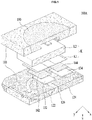
- FIG. 1 is a perspective view of a light emitting device package 100A according to an embodiment
- FIG. 2 is a sectional view of the light emitting device package 100A illustrated in FIG. 1 . That is, FIG. 2 corresponds to a cross sectional view of the light emitting device package 100A illustrated in FIG. 1 , which is taken in the direction of the z-axis and is viewed from the positive direction of the x-axis.
- the light emitting device package 100A illustrated in FIG. 1 may include a package body 110, first and second lead frames 122 and 124, an insulator 126, first and second solders 132 and 134, first and second pads 142 and 144, a light emitting device K, and a molding member 190.
- the package body 110 may define a cavity C.
- the package body 110 may define the cavity C along with the first and second lead frames 122 and 124. That is, the cavity C may be defined by a side surface 112 of the package body 110 and upper surfaces 122A and 124A of the first and second lead frames 122 and 124.
- the embodiment is not limited thereto.
- the cavity C may be defined only by the package body 110, unlike the illustration of FIGs. 1 and 2 .
- a barrier wall (not illustrated) may be disposed on the flat upper surface of the package body 110, and the cavity may be defined by the barrier wall and the upper surface of the package body 110.
- the package body 110 may be formed of, for example, an Epoxy Molding Compound (EMC), the embodiment is not limited to the material of the package body 110.
- EMC Epoxy Molding Compound
- the first and second lead frames 122 and 124 may be spaced apart from each other in the y-axis, which is perpendicular to the thickness direction of a light emitting structure 170.
- Each of the first and second lead frames 122 and 124 may be formed of a conductive material, for example, a metal, and the embodiment is not limited to the kinds of materials of the respective first and second lead frames 122 and 124.
- the insulator 126 may be located between the first and second lead frames 122 and 124, in order to electrically isolate the first and second lead frames 122 and 124 from each other.
- the first and second lead frames 122 and 124 may constitute a portion of the package body 110.
- the first and second lead frames 122 and 124 forming the package body 110 may be electrically isolated from each other by the insulator 126.
- the first solder 132 may be located between the first lead frame 122 and the first pad 142 so as to electrically connect the two 122 and 142 to each other.
- the second solder 134 may be located between the second lead frame 124 and the second pad 144 so as to electrically connect the two 124 and 144 to each other.
- Each of the first and second solders 132 and 134 may be solder paste or solder balls.
- the first and second solders 132 and 134 may eliminate the necessity of wires by electrically connecting first and second conductive semiconductor layers 172 and 176 of the light emitting device K to the first and second lead frames 122 and 124 respectively via the first and second pads 142 and 144.
- the first and second conductive semiconductor layers 172 and 176 may be connected respectively to the first and second lead frames 122 and 124 using wires.
- the light emitting device K may be placed inside the cavity C.
- the light emitting device K may be divided into a lower portion K1 and an upper portion K2.
- the lower portion K1 of the light emitting device K may include first insulation layers 152, 154 and 156, a first contact layer 162, and a second contact layer 164, and the upper portion K2 of the light emitting device K may include the light emitting structure 170 and a substrate 180A.
- the light emitting structure 170 may be displaced under the substrate 180A.
- the substrate 180A may comprise a conductive material or nonconductive material.
- the substrate 180A may comprise at least one of sapphire (Al 2 O 3 ), GaN, SiC, ZnO, GaP, InP, Ga 2 O 3 , GaAs, or Si, although the embodiment is not limited to the material of the substrate 180A.
- a buffer layer (or a transition layer)(not illustrated) may be further disposed between the two 180A and 170.
- the buffer layer may comprise at least one material selected from the group consisting of Al, In, N, and Ga, without being limited thereto.
- the buffer layer may have a single layer or multi-layer structure.
- the light emitting structure 170 may include a first conductive semiconductor layer 172, an active layer 174, and a second conductive semiconductor layer 176.
- the light emitting structure 170 may be disposed between the substrate 180A and the first and second lead frames 122 and 124.
- the first conductive semiconductor layer 172, the active layer 174, and the second conductive semiconductor layer 176 may be stacked one above another in sequence in the direction from the substrate 180A toward the first and second lead frames 122 and 124, i.e. in the positive direction of the +z-axis.
- the first conductive semiconductor layer 172 may be implemented in, for example, group III-V or II-VI compound semiconductors doped with a first conductive dopant.
- the first conductive dopant may be an n-type dopant, and comprise Si, Ge, Sn, Se, or Te, without being limited thereto.
- the first conductive semiconductor layer 172 may be disposed under the substrate 180A, and may comprise a semiconductor material having a composition of Al x In y Ga (i-x-y) N (0 ⁇ x ⁇ 1, 0 ⁇ y ⁇ 1, 0 ⁇ x+y ⁇ 1).
- the first conductive semiconductor layer 172 may comprise any one or more materials selected from among GaN, InN, AlN, InGaN, AlGaN, InAlGaN, AlInN, AlGaAs, InGaAs, AlInGaAs, GaP, AlGaP, InGaP, AlInGaP, and InP.
- the active layer 174 is disposed between the first conductive semiconductor layer 172 and the second conductive semiconductor layer 176.
- the active layer 124 is a layer in which electrons (or holes) injected through the first conductive semiconductor layer 172 and holes (or electrons) injected through the second conductive semiconductor layer 176 meet each other to emit light having energy determined by an inherent energy band of a constituent material of the active layer 174.
- the active layer 174 may be formed into at least one structure selected from among a single-well structure, a multi-well structure, a single-quantum well structure, a multi-quantum well structure, a quantum dot structure, and a quantum wire structure.
- the active layer 174 may include a well layer and a barrier layer having a pair structure of any one or more of InGaN/GaN, InGaN/InGaN, GaN/AlGaN, InAlGaN/GaN, GaAs(InGaAs)/AlGaAs, and GaP(InGaP)/AlGaP, without being limited thereto.
- the well layer may be formed of a material having lower band gap energy than the band gap energy of the barrier layer.
- a conductive clad layer may be formed above and/or under the active layer 174.
- the conductive clad layer may be formed of semiconductors having higher band gap energy than the band gap energy of the barrier layer of the active layer 174.
- the conductive clad layer may include GaN, AlGaN, InAlGaN, or a super lattice structure.
- the conductive clad layer may be doped with an n-type or p-type dopant.
- the active layer 174 may emit ultraviolet light having a specific wavelength band.
- the ultraviolet light wavelength band may be within a range from 100 nm to 400 nm.
- the active layer 174 may emit light having a wavelength band within a range from 100 nm to 280 nm.
- the embodiment is not limited to the wavelength band of light emitted from the active layer 174.
- the second conductive semiconductor layer 176 may be disposed under the active layer 174 and may be formed of a semiconductor compound.
- the second conductive semiconductor layer 176 may be formed of, for example, group III-V or II-VI compound semiconductors.
- the second conductive semiconductor layer 176 may comprise a semiconductor material having a composition of In x Al y Ga 1-x-y N (0 ⁇ x ⁇ 1, 0 ⁇ y ⁇ 1, 0 ⁇ x+y ⁇ 1).
- the second conductive semiconductor layer 176 may be doped with a second conductive dopant.
- the second conductive dopant may be a p-type dopant and may include, for example, Mg, Zn, Ca, Sr, or Ba.
- the first conductive semiconductor layer 172 may be an n-type semiconductor layer, and the second conductive semiconductor layer 176 may be a p-type semiconductor layer.
- the first conductive semiconductor layer 172 may be a p-type semiconductor layer, and the second conductive semiconductor layer 176 may be an n-type semiconductor layer.
- the light emitting structure 170 may be implemented in any one structure selected from among an n-p junction structure, a p-n junction structure, an n-p-n junction structure, and a p-n-p junction structure.
- the light emitting device package 100A illustrated in FIGs. 1 and 2 has a flip chip bonding structure, and therefore light emitted from the active layer 174 may be emitted through the first contact layer 162, the first conductive semiconductor layer 172, and the substrate 180A.
- the first contact layer 162, the first conductive semiconductor layer 172, and the substrate 180A may be formed of a light transmissive material.
- the second conductive semiconductor layer 176 and the second contact layer 164 may be formed of a transmissive or non-transmissive material, or a reflective material, the embodiment may not be limited to a specific material. The material of each of the first and second contact layers 162 and 164 will be described below in detail.
- the first contact layer 162 may be disposed between the first conductive semiconductor layer 172 and the first pad 142, so as to electrically connect the first conductive semiconductor layer 172 and the first pad 142 to each other.
- the first contact layer 162 may comprise an ohmic contact material, and serve as an ohmic layer. Thus, a separate ohmic layer (not illustrated) may be unnecessary, or a separate ohmic layer may be disposed above or under the first contact layer 162.
- the second contact layer 164 may be disposed between the second conductive semiconductor layer 176 and the second pad 144, so as to electrically connect the second conductive semiconductor layer 176 and the second pad 144 to each other. To this end, as illustrated, the second contact layer 164 may come into contact with the second conductive semiconductor layer 176.
- Each of the first and second contact layers 162 and 164 may reflect or transmit light emitted from the active layer 174, rather than absorbing the light, and may be formed of any material that is capable of growing in good quality on the first and second conductive semiconductor layers 172 and 176.
- each of the first and second contact layers 162 and 164 may be formed of a metal, and may be formed of Ag, Ni, Al, Rh, Pd, Ir, Ru, Mg, Zn, Pt, Au, Hf, and selective combinations thereof.
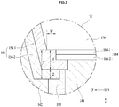
- FIG. 3 is an enlarged sectional view of portion 'A' illustrated in FIG. 2 .
- the second contact layer 164 may comprise a reflective material.
- the second contact layer 164 may include a transparent electrode 164-1 and a reflective layer 164-2.
- the reflective layer 164-2 may be formed of a reflective material such as silver (Ag).
- the transparent electrode 164-1 may be disposed between the reflective layer 164-2 and the second conductive semiconductor layer 176, and the reflective layer 164-2 may be disposed under the transparent electrode 164-1.
- the transparent electrode 164-1 may be a Transparent Conductive Oxide (TCO) film.
- the transparent electrode 164-1 may comprise at least one of Indium Tin Oxide (ITO), Indium Zinc Oxide (IZO), Indium Zinc Tin Oxide (IZTO), Indium Aluminum Zinc Oxide (IAZO), Indium Gallium Zinc Oxide (IGZO), Indium Gallium Tin Oxide (IGTO), Aluminum Zinc Oxide (AZO), Antimony Tin Oxide (ATO), Gallium Zinc Oxide (GZO), IrOx, RuOx, RuOx/ITO, Ni/IrOx/Au, or Ni/IrOx/Au/ITO, and is not limited to these materials.
- ITO Indium Tin Oxide
- IZO Indium Zinc Oxide
- IZTO Indium Zinc Tin Oxide
- IAZO Indium Aluminum Zinc Oxide
- IGZO Indium Gallium Zinc Oxide
- IGTO Indium Gallium Tin Oxide
- ATO Antimony Tin Oxide
- GZO Gallium Zinc Oxide
- the second contact layer 164 may have ohmic characteristics and may comprise a material for ohmic contact with the second conductive semiconductor layer 176.
- a separate ohmic layer (not illustrated) may not be formed.
- the first pad 142 may be disposed between the first solder 132 and the first conductive semiconductor layer 172, so as to electrically connect the first solder 132 and the first conductive semiconductor layer 172 to each other.
- the first pad 142 may be implemented in the form of a penetration electrode that penetrates the second conductive semiconductor layer 176 and the active layer 174 so as to be electrically connected to the first conductive semiconductor layer 172, the embodiment is not limited thereto. That is, in another embodiment, although not illustrated, the first pad 142 may bypass the second conductive semiconductor layer 176 and the active layer 174 to thereby be electrically connected to the first conductive semiconductor layer 172. As such, the first pad 142 may serve as a first electrode.
- the second pad 144 may be disposed between the second solder 134 and the second conductive semiconductor layer 176, so as to electrically connect the second solder 134 and the second conductive semiconductor layer 176 to each other.
- the second pad 144 may be implemented in the form of a penetration electrode that penetrates the first insulation layers 154 and 156 so as to come into contact with the second contact layer 164, the embodiment is not limited thereto. That is, in another embodiment, the second pad 144 may be connected to the second contact layer 164 without penetrating the first insulation layers 154 and 156. As such, the second pad 144 may serve as a second electrode.
- Each of the first and second pads 142 and 144 may comprise an electrode material.
- the first insulation layers 152 and 154 may be disposed between the second conductive semiconductor layer 176 and the first pad 142, so as to electrically insulate the second conductive semiconductor layer 176 and the first pad 142 from each other.
- the first insulation layers 152 and 154 may be disposed between the active layer 174 and the first pad 142, so as to electrically insulate the active layer 174 and the first pad 142 from each other.
- the first insulation layer 152 may be located for the capping of the side portion and the upper portion of the second contact layer 164.
- each of the first insulation layers 152, 154, and 156 takes, in accordance with the invention, the form of a multi-layer structure including at least two layers.
- the first insulation layer 154 includes two layers such as a first-first insulation layer 154-1 and a first-second insulation layer 154-2.
- each of the first insulation layers 152, 154 and 156 may be configured such that multiple layers including at least two layers are repeated.
- the first insulation layer 154 may be configured such that the first-first insulation layer 154-1 and the first-second insulation layer 154-2 are repeatedly stacked one above another.
- the at least two layers constituting each of the first insulation layers 152, 154 and 156 are formed of materials having different coefficients of thermal expansion (CTE).
- CTE coefficients of thermal expansion
- Each of the at least two layers constituting each of the first insulation layers 152, 154 and 156 may comprise at least one of SiO 2 , TiO 2 , ZrO 2 , Si 3 N 4 , Al 2 O 3 , or MgF 2 .
- the coefficient of thermal expansion (CTE) of SiO 2 , TiO 2 , ZrO 2 , Si 3 N 4 , Al 2 O 3 , and MgF 2 may respectively be 0.55 x 10 -6 /K, 9 x 10 -6 /K, 8.5 x 10 -6 /K, 2.5 x 10 -6 /K, 7.5 x 10 -6 /K, and 10 to 15 x 10 -6 /K.
- the first average value the difference between the average value of the coefficients of cubic(or, volumetric) thermal expansion CTE AVE (hereinafter referred to as the "first average value") of the at least two layers constituting each of the first insulation layers 152, 154 and 156 and a first coefficient of thermal expansion of the substrate 180A is less than ⁇ 3 x 10 -6 /K or greater than ⁇ 9 x 10 -6 /K, there is a likelihood that there is sufficient residual stress to destroy the first insulation layers 152, 154 and 156.
- the difference between the first coefficient of thermal expansion of the substrate 180A and the first average value is within a range from ⁇ 3 x 10 -6 /K to ⁇ 9 x 10 - 6 /K, and for example, ⁇ 4 x 10 -6 /K or less, the embodiment is not limited thereto.
- the difference between the first coefficient of thermal expansion of the substrate 180A and the first average value is within a range from ⁇ 2.5 x 10 -6 /K to ⁇ 12.5 x 10 -6 /K, and for example, ⁇ 5 x 10 -6 /K or less.
- CTE AVG V 1 V 1 + V 2 ⁇ CTE 1 + V 2 V 1 + V 2 ⁇ CTE 2
- V1 is the volume of the first material
- V2 is the volume of the second material
- CTE1 is the CTE of the first material
- CTE2 is the CTE of the second material.
- the difference between the first average value and the average value of the coefficient of cubic thermal expansion of the upper portion K2 of the light emitting device K (hereinafter referred to as the "second average value") is within a range from ⁇ 3 x 10 -6 /K to ⁇ 9 x 10 -6 /K, and for example, ⁇ 4 x 10 -6 /K or less, although the embodiment is not limited thereto.
- the difference between the coefficients of thermal expansion (or, average values) between the case (hereinafter referred to as a "Comparative Example") where the first insulation layers 152, 154 and 156 are replaced with a single layer and the case (hereinafter respectively referred to as a "First Example” and a “Second Example”) where each of the first insulation layers 152, 154 and 156 has a multilayer structure as in the embodiment may be as in the following Table 1.
- each of CTE and CTE AVG is 10 -6 /K
- the values 3.9 and 5.5 of the first insulation layers 152, 154 and 156 in First Example and Second Example represent first average values CTE AVG .
- the first average value may be adjusted by varying the first and second thicknesses t1 and t2 of, for example, the layers 154-1 and 154-2 constituting the first insulation layer 154.
- the volume of the first-first insulation layer 154-1 and the volume of the first-second insulation layer 154-2 may vary according to the first and second thicknesses t1 and t2, assuming that the sizes of planes parallel to the x-axis and the y-axis are the same as each other.
- the at least two layers constituting each of the first insulation layers 152, 154 and 156 may have different thicknesses.
- the first thickness t1 of the first-first insulation layer 154-1 and the second thickness t2 of the first-second insulation layer 154-2 may be different from each other.
- the width W of the first-first insulation layer 154-1 overlapping the top of the second conductive semiconductor layer 176 in the z-axis, i.e. in the vertical direction may be approximately 3 ⁇ m in consideration of a process margin, the embodiment is not limited thereto.
- the first insulation layers 152, 154 and 156 may be implemented into a Distributed Bragg Reflector (DBR).
- DBR Distributed Bragg Reflector
- the DBR may perform an insulation function, and may perform a reflection function.
- the DBR may be configured in a manner such that a first layer and a second layer, which have different indices of refraction, are alternately stacked one above another at least once.
- the DBR may be an electrical insulation material.
- the first layer may include a first dielectric layer such as TiO 2
- the second layer may include a second dielectric layer such as SiO 2 .
- the DBR may take the form of a stack of at least one pair of TiO 2 /SiO 2 layers.
- Each of the first layer and the second layer may have a thickness of ⁇ /4, and ⁇ may be the wavelength of light generated in a light emitting cell.
- the total thickness (e.g., T) of each of the first insulation layers 152, 154 and 156 may not perform an insulation function.
- the total thickness (e.g., T) of each of the first insulation layers 152, 154 and 156 may be greater than 10 ⁇ m, this may cause difficulties with regard to manufacturing processes. Accordingly, the total thickness (e.g., T) of each of the first insulation layers 152, 154 and 156 may be within a range from 0.5 ⁇ m to 10 ⁇ m, and for example, may be within a range from 1 ⁇ m to 3 ⁇ m.
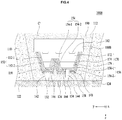
- FIG. 4 is a sectional view of a light emitting device package 100B according to another embodiment
- FIG. 5 is a local plan view of the light emitting device package 100B illustrated in FIG. 4
- FIG. 5 is a plan view of the light emitting device package 100B viewed in the +z-axis after deposition of metal layers 146 and 148.
- FIG. 6 is an enlarged plan view of portion 'B' illustrated in FIG. 5 .
- reference numeral 140 designates the first or second pad 142 or 144
- reference numeral 150 designates the first insulation layers 152, 154 and 156
- reference character "H” designates the metal layer 146 that penetrates the second conductive semiconductor layer 176, the active layer 174, and a portion of the first conductive semiconductor layer 172.
- the first insulation layers 150; 152, 154 and 156, the second contact layer 164, the metal layers 146 and 148, and a second insulation layer 158 may correspond to the lower portion K1 of the light emitting device K illustrated in FIG. 1
- the substrate 180B and the light emitting structure 170 may correspond to the upper portion K2 of the light emitting device K illustrated in FIG. 1
- the light emitting device package 100B is illustrated as not including the first contact layer 162 illustrated in FIG. 2 , in another embodiment, the light emitting device package 100B may include the first contact layer 162 disposed in the shape illustrated in FIG. 2 .
- a first electrode of the light emitting device package 100B illustrated in FIG. 4 may include the metal layers 146 and 148 and the bonding pad 142.
- the metal layer 146 may penetrate the second conductive semiconductor layer 176, the active layer 174, and a portion of the first conductive semiconductor layer 172, so as to be electrically connected to the first conductive semiconductor layer 172.
- the metal layers 146 and 148 may be electrically isolated from the second conductive semiconductor layer 176 and the active layer 174 by the first insulation layers 152, 154 and 156.
- the light emitting device package 100B illustrated in FIG. 4 may further include the second insulation layer 158.
- the second insulation layer 158 may be disposed to enclose the first insulation layers 152, 154 and 156 and the metal layer 146.
- the bonding pad 142 may penetrate the second insulation layer 158 to thereby be electrically connected to (or electrically come into contact with) the metal layer 146
- the second pad 144 corresponding to a second electrode may penetrate the first and second insulation layers 154, 156 and 158 and the metal layers 146 and 148 to thereby be electrically connected to (or electrically come into contact with) the second contact layer 164.
- the bonding pad 142 and the second pad 144 in FIG. 4 are described using the same reference numerals as the first and second pads 142 and 144 illustrated in FIGs. 1 and 2 .
- the bonding pad 142 illustrated in FIG. 4 is the same as the first pad 142 illustrated in FIGs. 1 and 2 except that the bonding pad 142 is electrically connected to the first conductive semiconductor layer 172 via the metal layer 146.
- the second pad 144 illustrated in FIG. 4 is the same as the second pad 144 illustrated in FIGs. 1 and 2 except that the second pad 144 penetrates the first insulation layers 154 and 156, the second insulation layer 158 and the metal layers 146 and 148 to thereby be electrically connected to the second contact layer 164.
- the substrate 180B illustrated in FIG. 4 may include a pattern 182 unlike the substrate 180A illustrated in FIG. 2 .
- the pattern 182 may have any of various cross-sectional shapes so as to assist light emitted from the active layer 174 in escaping from the light emitting device package 100B.
- the substrate 180B may be a Patterned Sapphire Substrate (PSS).
- PSS Patterned Sapphire Substrate
- the substrate 180A illustrated in FIG. 2 may also have the pattern 182.
- the light emitting device package 100B illustrated in FIGs. 4 and 5 is the same as the light emitting device package 100A illustrated in FIGs. 1 and 2 except for the above-described differences, and thus has been described using the same reference numerals, and a repeated description of the same configurations is omitted.
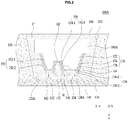
- FIG. 7 is a planar photograph of a light emitting device package according to a comparative embodiment.
- the first insulation layers 152, 154 and 156 illustrated in the light emitting device packages 100A and 100B according to the embodiments illustrated in FIGs. 1 , 2 , 4 and 5 are replaced with a single layer.
- the first insulation layer in the form of a single layer may be destroyed by residual stress after a flip-chip bonding process. The destruction of the first insulation layer 152, 154, or 156 may cause the second conductive semiconductor layer 176 to be exposed as illustrated in FIG. 7 .
- each of the first insulation layers 152, 154 and 156 has a low coefficient of thermal expansion
- the second contact layer 164 and the second pad 144 disposed above and under the first insulation layers 152, 154 and 156, respectively have high coefficients of thermal expansion.
- the coefficient of thermal expansion of the second contact layer 164 and the second pad 144 which are formed of a metal such as gold (Au) generally has a relatively high value of 14.16 x 10 -6 K, whereas the first insulation layers 152, 154 and 156, which have the form of a single layer formed of an insulation material such as SiO 2 , have a relatively low coefficient of thermal expansion, for example, 0.5 x 10 -6 /K.
- each of the first insulation layers 152, 154 and 156 of the light emitting device packages 100A and 100B according to the embodiments has a multilayer structure including at least two layers
- each of the first insulation layers 152, 154 and 156 may have a higher coefficient of thermal expansion than the insulation layer having a single layer structure according to the comparative embodiment, thereby being free from destruction due to residual stress after a flip-chip bonding process.
- the reflectance in a region at which the second contact layer 164 is not present may be enhanced by the DBR because the DBR can reflect light.
- the above-described second contact layer 164 illustrated in FIG. 3 includes the transparent electrode 164-1 formed of ITO and the reflective layer 164-2 formed of silver (Ag), silver (Ag) has good reflectance, but poor adhesion.
- peeling of the metal e.g., silver (Ag)
- the metal may occur at the interface between the ITO 164-1 and the reflective layer 164-2 illustrated in FIG. 3 due to the difference in coefficient of thermal expansion.
- the first insulation layers 150; 152, 154 and 156 may be manufactured using, for example, Plasma Enhanced Chemical Vapor Deposition (PECVD) so as to enable the capping of the second contact layer 164, thereby improving the poor adhesion of silver so that the metal may be prevented from peeling.
- PECVD Plasma Enhanced Chemical Vapor Deposition
- the high density characteristics of the IAD thin layer may prevent the migration of silver (Ag) from the reflective layer 164-2 and improve the adhesion at the interface between the light emitting structure 170 and the first insulation layers 152, 154 and 156.
- the first insulation layers 150; 152, 154 and 156 have a multilayer structure, as exemplarily illustrated in FIG. 3 , even if a crack is generated at a stepped corner portion of the second contact layer 164, the first insulation layers 150; 152, 154 and 156 have a multilayer structure, thereby effectively preventing negative effects due to the crack.
- the molding member 190 of the light emitting device packages 100A and 100B may enclose and protect the light emitting device K.
- the molding member 190 may be formed of, for example, silicon (Si) and contain phosphors, thus being capable of changing the wavelength of light emitted from the light emitting device K.
- the phosphors may include phosphors selected from among YAG-based, TAG-based, silicate-based, sulfide-based, and nitride-based wavelength change materials which may change light generated from the light emitting device K into white light, the embodiment is not limited to the kinds of phosphors.
- the YGA-based and TAG-based phosphors may be selected from among (Y, Tb, Lu, Sc, La, Gd, Sm)3(Al, Ga, In, Si, Fe)5(O, S)12:Ce, and the silicate-based phosphors may be selected from among (Sr, Ba, Ca, Mg)2SiO4:(Eu, F, Cl).
- the sulfide-based phosphors may be selected from among (Ca, Sr)S:Eu, (Sr, Ca, Ba)(Al, Ga)2S4:Eu
- the nitride-based phosphors may be selected from among (Sr, Ca, Si, Al, O)N:Eu (e.g., CaAlSiN4:Eu ⁇ -SiAlON:Eu) or Ca- ⁇ SiAlON:Eu-based (Cax, My)(Si, Al)12(O, N)16 (here, M is at least one of Eu, Tb, Yb, or Er, 0.05 ⁇ (x+y) ⁇ 0.3, 0.02 ⁇ x ⁇ 0.27, and 0.03 ⁇ y ⁇ 0.3).
- Red phosphors may be nitride-based phosphors including N(e.g., CaAISiN3:Eu).
- the nitride-based red phosphors have higher reliability in resistance to external environments such as, for example, heat and moisture and lower discoloration risk than sulfide-based phosphors.
- the embodiment is not limited thereto. That is, in another embodiment, the present invention may also be applied to a light emitting device package having a vertical bonding structure.
- an array of a plurality of light emitting device packages may be disposed on a board, and optical members such as, for example, a light guide plate, a prism sheet, and a diffuser sheet may be disposed in an optical path of the light emitting device packages.
- optical members such as, for example, a light guide plate, a prism sheet, and a diffuser sheet may be disposed in an optical path of the light emitting device packages.
- the light emitting device packages, the board, and the optical members may function as a backlight unit.
- the light emitting device package according to the embodiment may be included in a light emitting apparatus such as, for example, a display apparatus, an indicator apparatus, and a lighting apparatus.
- the display apparatus may include a bottom cover, a reflective plate disposed on the bottom cover, a light emitting module configured to emit light, a light guide plate disposed in front of the reflective plate to forwardly guide light emitted from the light emitting module, optical sheets including prism sheets disposed in front of the light guide plate, a display panel disposed in front of the optical sheets, an image signal output circuit connected to the display panel to supply an image signal to the display panel, and a color filter disposed in front of the display panel.
- the bottom cover, the reflective plate, the light emitting module, the light guide plate, and the optical sheets may constitute a backlight unit.
- the lighting apparatus may include a light source module which includes a board and the light emitting device package according to the embodiment, a radiator configured to radiate heat of the light source module, and a power supply unit configured to process or convert an electrical signal from an external source so as to supply the same to the light source module.
- the lighting apparatus may include a lamp, a headlamp, or a streetlight.
- the headlamp may include a light emitting module which includes the light emitting device packages arranged on a board, a reflector configured to reflect light, emitted from the light source module, in a given direction, for example, forwardly, a lens configured to forwardly refract light reflected by the reflector, and a shade configured to achieve a light distribution pattern selected by a designer by blocking or reflecting some of light, reflected by the reflector and directed to the lens.
- a light emitting module which includes the light emitting device packages arranged on a board, a reflector configured to reflect light, emitted from the light source module, in a given direction, for example, forwardly, a lens configured to forwardly refract light reflected by the reflector, and a shade configured to achieve a light distribution pattern selected by a designer by blocking or reflecting some of light, reflected by the reflector and directed to the lens.
- a light emitting device package is capable of preventing a first insulation layer from being destroyed by residual stress after flip chip bonding by reducing the difference in coefficient of thermal expansion between a substrate and the first insulation layer.
- the light emitting device is capable of preventing the peeling of metal at the interface between a reflective layer and a transparent electrode included in a second contact layer and preventing the migration of metal included in the reflective layer.
- the light emitting device is capable of increasing the adhesion between a light emitting structure and the first insulation layer and, thanks to the reflective layer included in the second contact layer, increasing reflectance in a region in which the reflection of light would otherwise be impossible.
- the light emitting device is capable of effectively preventing negative effects even if a crack is generated at a stepped corner portion of the second contact layer.
Landscapes
- Engineering & Computer Science (AREA)
- Microelectronics & Electronic Packaging (AREA)
- Manufacturing & Machinery (AREA)
- Computer Hardware Design (AREA)
- Power Engineering (AREA)
- Led Devices (AREA)
- Led Device Packages (AREA)
Description
- Embodiments relate to a light emitting diode package and a light emitting apparatus including the package.
- Light Emitting Diodes (LEDs) are semiconductor devices that convert electricity into light using characteristics of compound semiconductors so as to enable transmission/reception of signals, or that are used as a light source.
- Group III-V nitride semiconductors are in the spotlight as core materials of light emitting devices such as, for example, LEDs or Laser Diodes (LDs) due to physical and chemical characteristics thereof.
- The LEDs do not include environmentally harmful materials such as mercury (Hg) that are used in conventional lighting appliances such as, for example, fluorescent lamps and incandescent bulbs, and thus are very eco-friendly, and have several advantages such as, for example, long lifespan and low power consumption. As such, conventional light sources are being rapidly replaced with LEDs. Meanwhile, a conventional light emitting device package is configured such that several layers having different coefficients of thermal expansion are stacked one above another. The difference in coefficients of thermal expansion may lead to the destruction of the light emitting device package.
- Examples of light emitting device packages and light emitting apparatuses according to the prior art are known from
US 2012/074441 . - The present invention relates to a light emitting diode package according to claim 1 and an apparatus according to claim 11.
- Embodiments as disclosed provide a light emitting diode package, which may achieve enhanced adhesion, may prevent the destruction of respective layers due to stress caused by the difference between the coefficients of thermal expansion of the different layers, and may have increased reflectance and improved reliability, and a light emitting apparatus including the package.
- In one embodiment, a light emitting diode package includes a substrate, a light emitting structure disposed under the substrate, the light emitting structure including a first conductivity type (in the following, the term "conductive" may be used instead of "conductivity type") semiconductor layer, an active layer, and a second conductive semiconductor layer, a first electrode configured to penetrate the second conductive semiconductor layer and the active layer, so as to come into contact with the first conductive semiconductor layer, a contact layer configured to come into contact with the second conductive semiconductor layer, a first insulation layer disposed between the second conductive semiconductor layer and the first electrode and between the active layer and the first electrode, the first insulation layer being provided for capping of a side portion and an upper portion of the contact layer, and a second electrode configured to penetrate the first insulation layer, so as to come into contact with the contact layer. According to the invention, the contact layer comprises a reflective material. The contact layer includes a reflective layer and a transparent electrode disposed between the reflective layer and the second conductive semiconductor layer. The reflective layer comprises silver (Ag).
- For example, the first electrode may include a metal layer configured to penetrate the second conductive semiconductor layer and the active layer, so as to come into contact with the first conductive semiconductor layer, and a bonding pad configured to come into contact with the metal layer. The light emitting device package may further include a second insulation layer disposed to enclose the first insulation layer and the metal layer, and the second electrode may penetrate the first and second insulation layers and the metal layer, so as to come into contact with the contact layer.
- According to the invention, the first insulation layer includes at least two layers. The first insulation layer may have a multilayer structure including the at least two layers repeatedly disposed. The at least two layers are formed of materials having different coefficients of thermal expansion. Each of the at least two layers may comprise at least one of SiO2, TiO2, ZrO2, Si3N4, Al2O3, and MgF2.
- For example, a difference between a first coefficient of thermal expansion of the substrate and an average value of coefficients of volumetric thermal expansion of the at least two layers may be ±3 x 10⁻⁶K or more. In addition, a difference between a first coefficient of thermal expansion of the substrate and an average value of coefficients of volumetric thermal expansion of the at least two layers may be ±4 x 10⁻⁶K or less.
- Alternatively, for example, the substrate may comprise sapphire, and a difference between a first coefficient of thermal expansion of the substrate and an average value of coefficients of volumetric thermal expansion of the at least two layers may be within a range from ±2.5 x 10⁻⁶K to ±12.5 x 10⁻⁶K.
- For example, the substrate may comprise sapphire, and a difference between a first coefficient of thermal expansion of the substrate and an average value of coefficients of volumetric thermal expansion of the at least two layers may be ±5 x 10⁻⁶K or less.
- For example, a difference between an average value of coefficients of volumetric thermal expansion of the substrate and the light emitting structure and an average value of coefficients of volumetric thermal expansion of the at least two layers may be within a range from ±3 x 10⁻⁶K to ±4 x 10⁻⁶K.
- For example, the at least two layers may have different thicknesses.
- For example, the first insulation layer may include a distributed bragg reflector.
- For example, the light emitting device package may further include first and second lead frames electrically isolated from each other, a first solder disposed between the first electrode and the first lead frame, and a second solder disposed between the second electrode and the second lead frame.
- For example, the first insulation layer may have a thickness within a range from 0.5µm to 10µm.
- In another embodiment, a light emitting apparatus includes the light emitting device package according to claim 1.
- Arrangements and embodiments may be described in detail with reference to the following drawings in which like reference numerals refer to like elements and wherein:
-
FIG. 1 is a perspective view of a light emitting device package according to an embodiment; -
FIG. 2 is a cross sectional view of the light emitting device package illustrated inFIG. 1 ; -
FIG. 3 is an enlarged sectional view of portion 'A' illustrated inFIG. 2 ; -
FIG. 4 is a sectional view of a light emitting device package according to another embodiment; -
FIG. 5 is a local plan view of the light emitting device package illustrated inFIG. 4 ; -
FIG. 6 is an enlarged plan view of portion 'B' illustrated inFIG. 5 ; and -
FIG. 7 is a planar photograph of a light emitting device package according to a comparative embodiment. - Hereinafter, exemplary embodiments will be described in detail with reference to the accompanying drawings to aid in understanding of the embodiments. However, the embodiments may be altered in various ways, and the scope of the embodiments should not be construed as limited to the following description. The embodiments are intended to provide those skilled in the art with more complete explanation.
- In addition, the relative terms "first", "second", "upper", "lower" and the like in the description and in the claims may be used to distinguish between any one substance or element and other substances or elements and not necessarily for describing any physical or logical relationship between the substances or elements or a particular order.
-
FIG. 1 is a perspective view of a lightemitting device package 100A according to an embodiment, andFIG. 2 is a sectional view of the lightemitting device package 100A illustrated inFIG. 1 . That is,FIG. 2 corresponds to a cross sectional view of the lightemitting device package 100A illustrated inFIG. 1 , which is taken in the direction of the z-axis and is viewed from the positive direction of the x-axis. - The light
emitting device package 100A illustrated inFIG. 1 may include apackage body 110, first andsecond lead frames insulator 126, first andsecond solders second pads molding member 190. - The
package body 110 may define a cavity C. For example, as exemplarily illustrated inFIGs. 1 and2 , thepackage body 110 may define the cavity C along with the first andsecond lead frames side surface 112 of thepackage body 110 andupper surfaces second lead frames package body 110, unlike the illustration ofFIGs. 1 and2 . Alternatively, a barrier wall (not illustrated) may be disposed on the flat upper surface of thepackage body 110, and the cavity may be defined by the barrier wall and the upper surface of thepackage body 110. Although thepackage body 110 may be formed of, for example, an Epoxy Molding Compound (EMC), the embodiment is not limited to the material of thepackage body 110. - The first and
second lead frames light emitting structure 170. Each of the first andsecond lead frames second lead frames insulator 126 may be located between the first andsecond lead frames second lead frames - In addition, when the
package body 110 is formed of a conductive material, for example, a metal material, the first andsecond lead frames package body 110. In this case, the first andsecond lead frames package body 110 may be electrically isolated from each other by theinsulator 126. - The
first solder 132 may be located between thefirst lead frame 122 and thefirst pad 142 so as to electrically connect the two 122 and 142 to each other. Thesecond solder 134 may be located between thesecond lead frame 124 and thesecond pad 144 so as to electrically connect the two 124 and 144 to each other. Each of the first andsecond solders - As described above, the first and
second solders conductive semiconductor layers second lead frames second pads - Meanwhile, the light emitting device K may be placed inside the cavity C. The light emitting device K may be divided into a lower portion K1 and an upper portion K2. The lower portion K1 of the light emitting device K may include first insulation layers 152, 154 and 156, a
first contact layer 162, and asecond contact layer 164, and the upper portion K2 of the light emitting device K may include thelight emitting structure 170 and asubstrate 180A. - The
light emitting structure 170 may be displaced under thesubstrate 180A. Thesubstrate 180A may comprise a conductive material or nonconductive material. For example, thesubstrate 180A may comprise at least one of sapphire (Al2O3), GaN, SiC, ZnO, GaP, InP, Ga2O3, GaAs, or Si, although the embodiment is not limited to the material of thesubstrate 180A. - In order to improve the difference in Coefficient of Thermal Expansion (CTE) and the lattice mismatch between the
substrate 180A and thelight emitting structure 170, a buffer layer (or a transition layer)(not illustrated) may be further disposed between the two 180A and 170. The buffer layer, for example, may comprise at least one material selected from the group consisting of Al, In, N, and Ga, without being limited thereto. In addition, the buffer layer may have a single layer or multi-layer structure. - The
light emitting structure 170 may include a firstconductive semiconductor layer 172, anactive layer 174, and a secondconductive semiconductor layer 176. Thelight emitting structure 170 may be disposed between thesubstrate 180A and the first and second lead frames 122 and 124. The firstconductive semiconductor layer 172, theactive layer 174, and the secondconductive semiconductor layer 176 may be stacked one above another in sequence in the direction from thesubstrate 180A toward the first and second lead frames 122 and 124, i.e. in the positive direction of the +z-axis. - The first
conductive semiconductor layer 172 may be implemented in, for example, group III-V or II-VI compound semiconductors doped with a first conductive dopant. When the firstconductive semiconductor layer 172 is an n-type semiconductor layer, the first conductive dopant may be an n-type dopant, and comprise Si, Ge, Sn, Se, or Te, without being limited thereto. - For example, the first
conductive semiconductor layer 172 may be disposed under thesubstrate 180A, and may comprise a semiconductor material having a composition of AlxInyGa(i-x-y)N (0≤x≤1, 0≤y≤1, 0≤x+y≤1). The firstconductive semiconductor layer 172 may comprise any one or more materials selected from among GaN, InN, AlN, InGaN, AlGaN, InAlGaN, AlInN, AlGaAs, InGaAs, AlInGaAs, GaP, AlGaP, InGaP, AlInGaP, and InP. - The
active layer 174 is disposed between the firstconductive semiconductor layer 172 and the secondconductive semiconductor layer 176. Theactive layer 124 is a layer in which electrons (or holes) injected through the firstconductive semiconductor layer 172 and holes (or electrons) injected through the secondconductive semiconductor layer 176 meet each other to emit light having energy determined by an inherent energy band of a constituent material of theactive layer 174. Theactive layer 174 may be formed into at least one structure selected from among a single-well structure, a multi-well structure, a single-quantum well structure, a multi-quantum well structure, a quantum dot structure, and a quantum wire structure. - The
active layer 174 may include a well layer and a barrier layer having a pair structure of any one or more of InGaN/GaN, InGaN/InGaN, GaN/AlGaN, InAlGaN/GaN, GaAs(InGaAs)/AlGaAs, and GaP(InGaP)/AlGaP, without being limited thereto. The well layer may be formed of a material having lower band gap energy than the band gap energy of the barrier layer. - A conductive clad layer (not illustrated) may be formed above and/or under the
active layer 174. The conductive clad layer may be formed of semiconductors having higher band gap energy than the band gap energy of the barrier layer of theactive layer 174. For example, the conductive clad layer may include GaN, AlGaN, InAlGaN, or a super lattice structure. In addition, the conductive clad layer may be doped with an n-type or p-type dopant. - In some embodiments, the
active layer 174 may emit ultraviolet light having a specific wavelength band. Here, the ultraviolet light wavelength band may be within a range from 100 nm to 400 nm. In particular, theactive layer 174 may emit light having a wavelength band within a range from 100 nm to 280 nm. However, the embodiment is not limited to the wavelength band of light emitted from theactive layer 174. - The second
conductive semiconductor layer 176 may be disposed under theactive layer 174 and may be formed of a semiconductor compound. The secondconductive semiconductor layer 176 may be formed of, for example, group III-V or II-VI compound semiconductors. For example, the secondconductive semiconductor layer 176 may comprise a semiconductor material having a composition of InxAlyGa1-x-yN (0≤x≤1, 0≤y≤1, 0≤x+y≤1). The secondconductive semiconductor layer 176 may be doped with a second conductive dopant. When the secondconductive semiconductor layer 176 is a p-type semiconductor layer, the second conductive dopant may be a p-type dopant and may include, for example, Mg, Zn, Ca, Sr, or Ba. - The first
conductive semiconductor layer 172 may be an n-type semiconductor layer, and the secondconductive semiconductor layer 176 may be a p-type semiconductor layer. Alternatively, the firstconductive semiconductor layer 172 may be a p-type semiconductor layer, and the secondconductive semiconductor layer 176 may be an n-type semiconductor layer. - The
light emitting structure 170 may be implemented in any one structure selected from among an n-p junction structure, a p-n junction structure, an n-p-n junction structure, and a p-n-p junction structure. - Since the light emitting
device package 100A illustrated inFIGs. 1 and2 has a flip chip bonding structure, and therefore light emitted from theactive layer 174 may be emitted through thefirst contact layer 162, the firstconductive semiconductor layer 172, and thesubstrate 180A. To this end, thefirst contact layer 162, the firstconductive semiconductor layer 172, and thesubstrate 180A may be formed of a light transmissive material. At this time, although the secondconductive semiconductor layer 176 and thesecond contact layer 164 may be formed of a transmissive or non-transmissive material, or a reflective material, the embodiment may not be limited to a specific material. The material of each of the first and second contact layers 162 and 164 will be described below in detail. - The
first contact layer 162 may be disposed between the firstconductive semiconductor layer 172 and thefirst pad 142, so as to electrically connect the firstconductive semiconductor layer 172 and thefirst pad 142 to each other. Thefirst contact layer 162 may comprise an ohmic contact material, and serve as an ohmic layer. Thus, a separate ohmic layer (not illustrated) may be unnecessary, or a separate ohmic layer may be disposed above or under thefirst contact layer 162. - The
second contact layer 164 may be disposed between the secondconductive semiconductor layer 176 and thesecond pad 144, so as to electrically connect the secondconductive semiconductor layer 176 and thesecond pad 144 to each other. To this end, as illustrated, thesecond contact layer 164 may come into contact with the secondconductive semiconductor layer 176. - Each of the first and second contact layers 162 and 164 may reflect or transmit light emitted from the
active layer 174, rather than absorbing the light, and may be formed of any material that is capable of growing in good quality on the first and second conductive semiconductor layers 172 and 176. For example, each of the first and second contact layers 162 and 164 may be formed of a metal, and may be formed of Ag, Ni, Al, Rh, Pd, Ir, Ru, Mg, Zn, Pt, Au, Hf, and selective combinations thereof. -
FIG. 3 is an enlarged sectional view of portion 'A' illustrated inFIG. 2 . - The
second contact layer 164 may comprise a reflective material. For example, referring toFIG. 3 , thesecond contact layer 164 may include a transparent electrode 164-1 and a reflective layer 164-2. - The reflective layer 164-2 may be formed of a reflective material such as silver (Ag).
- The transparent electrode 164-1 may be disposed between the reflective layer 164-2 and the second
conductive semiconductor layer 176, and the reflective layer 164-2 may be disposed under the transparent electrode 164-1. The transparent electrode 164-1 may be a Transparent Conductive Oxide (TCO) film. For example, the transparent electrode 164-1 may comprise at least one of Indium Tin Oxide (ITO), Indium Zinc Oxide (IZO), Indium Zinc Tin Oxide (IZTO), Indium Aluminum Zinc Oxide (IAZO), Indium Gallium Zinc Oxide (IGZO), Indium Gallium Tin Oxide (IGTO), Aluminum Zinc Oxide (AZO), Antimony Tin Oxide (ATO), Gallium Zinc Oxide (GZO), IrOx, RuOx, RuOx/ITO, Ni/IrOx/Au, or Ni/IrOx/Au/ITO, and is not limited to these materials. - The
second contact layer 164 may have ohmic characteristics and may comprise a material for ohmic contact with the secondconductive semiconductor layer 176. When thesecond contact layer 164 serves as an ohmic layer, a separate ohmic layer (not illustrated) may not be formed. - Meanwhile, the
first pad 142 may be disposed between thefirst solder 132 and the firstconductive semiconductor layer 172, so as to electrically connect thefirst solder 132 and the firstconductive semiconductor layer 172 to each other. As exemplarily illustrated inFIGs. 1 and2 , although thefirst pad 142 may be implemented in the form of a penetration electrode that penetrates the secondconductive semiconductor layer 176 and theactive layer 174 so as to be electrically connected to the firstconductive semiconductor layer 172, the embodiment is not limited thereto. That is, in another embodiment, although not illustrated, thefirst pad 142 may bypass the secondconductive semiconductor layer 176 and theactive layer 174 to thereby be electrically connected to the firstconductive semiconductor layer 172. As such, thefirst pad 142 may serve as a first electrode. - The
second pad 144 may be disposed between thesecond solder 134 and the secondconductive semiconductor layer 176, so as to electrically connect thesecond solder 134 and the secondconductive semiconductor layer 176 to each other. At this time, although thesecond pad 144 may be implemented in the form of a penetration electrode that penetrates the first insulation layers 154 and 156 so as to come into contact with thesecond contact layer 164, the embodiment is not limited thereto. That is, in another embodiment, thesecond pad 144 may be connected to thesecond contact layer 164 without penetrating the first insulation layers 154 and 156. As such, thesecond pad 144 may serve as a second electrode. - Each of the first and
second pads - Meanwhile, the first insulation layers 152 and 154 may be disposed between the second
conductive semiconductor layer 176 and thefirst pad 142, so as to electrically insulate the secondconductive semiconductor layer 176 and thefirst pad 142 from each other. In addition, the first insulation layers 152 and 154 may be disposed between theactive layer 174 and thefirst pad 142, so as to electrically insulate theactive layer 174 and thefirst pad 142 from each other. At this time, thefirst insulation layer 152 may be located for the capping of the side portion and the upper portion of thesecond contact layer 164. - According to the embodiment, each of the first insulation layers 152, 154, and 156 takes, in accordance with the invention, the form of a multi-layer structure including at least two layers. According to the invention, as exemplarily illustrated in
FIG. 3 , thefirst insulation layer 154 includes two layers such as a first-first insulation layer 154-1 and a first-second insulation layer 154-2. - Alternatively, each of the first insulation layers 152, 154 and 156 may be configured such that multiple layers including at least two layers are repeated. For example, as exemplarily illustrated in
FIG. 3 , thefirst insulation layer 154 may be configured such that the first-first insulation layer 154-1 and the first-second insulation layer 154-2 are repeatedly stacked one above another. - At this time, the at least two layers constituting each of the first insulation layers 152, 154 and 156 are formed of materials having different coefficients of thermal expansion (CTE). Referring to
FIG. 3 , the coefficient of thermal expansion of the first-first insulation layer 154-1 and the coefficient of thermal expansion of the first-second insulation layer 154-2 differ from each other. - Each of the at least two layers constituting each of the first insulation layers 152, 154 and 156 may comprise at least one of SiO2, TiO2, ZrO2, Si3N4, Al2O3, or MgF2. Here, the coefficient of thermal expansion (CTE) of SiO2, TiO2, ZrO2, Si3N4, Al2O3, and MgF2 may respectively be 0.55 x 10⁻⁶/K, 9 x 10⁻⁶/K, 8.5 x 10⁻⁶/K, 2.5 x 10⁻⁶/K, 7.5 x 10⁻⁶/K, and 10 to 15 x 10-6/K.
- At this time, when the difference between the average value of the coefficients of cubic(or, volumetric) thermal expansion CTEAVE (hereinafter referred to as the "first average value") of the at least two layers constituting each of the first insulation layers 152, 154 and 156 and a first coefficient of thermal expansion of the
substrate 180A is less than ±3 x 10⁻⁶/K or greater than ±9 x 10⁻⁶/K, there is a likelihood that there is sufficient residual stress to destroy the first insulation layers 152, 154 and 156. Accordingly, although the difference between the first coefficient of thermal expansion of thesubstrate 180A and the first average value is within a range from ±3 x 10⁻⁶/K to ±9 x 10- 6/K, and for example, ±4 x 10⁻⁶/K or less, the embodiment is not limited thereto. - Alternatively, when the
substrate 180A is formed of sapphire, the difference between the first coefficient of thermal expansion of thesubstrate 180A and the first average value is within a range from ±2.5 x 10⁻⁶/K to ±12.5 x 10⁻⁶/K, and for example, ±5 x 10⁻⁶/K or less. - Generally, the average value CTEAVE of coefficients of cubic thermal expansion of first and second materials may be represented by the following Equation 1.

- Here, V1 is the volume of the first material, V2 is the volume of the second material, CTE1 is the CTE of the first material, and CTE2 is the CTE of the second material.
- In addition, the difference between the first average value and the average value of the coefficient of cubic thermal expansion of the upper portion K2 of the light emitting device K (hereinafter referred to as the "second average value") is within a range from ±3 x 10⁻⁶/K to ±9 x 10⁻⁶/K, and for example, ±4 x 10⁻⁶/K or less, although the embodiment is not limited thereto.
- When the
substrate 180A is formed of sapphire, thelight emitting structure 170 is formed of GaN, and the reflective layer of thesecond contact layer 164 is formed of silver (Ag), the difference between the coefficients of thermal expansion (or, average values) between the case (hereinafter referred to as a "Comparative Example") where the first insulation layers 152, 154 and 156 are replaced with a single layer and the case (hereinafter respectively referred to as a "First Example" and a "Second Example") where each of the first insulation layers 152, 154 and 156 has a multilayer structure as in the embodiment may be as in the following Table 1.[Table 1] Classification Comparative Example First Example Second Example CTE CTEAVG CTE(CTEAVG) CTEAVG CTE(CTEAVG) CTEAVG K2 Substrate (180A) 7.5 7.4 7.5 7.4 7.5 7.4 Light Emitting Structure (170) 5.6 5.6 5.6 K1 Second Contact Layer (164) 13.4 8.9 13.4 7.2 13.4 7.8 First Insulation Layer 0.55 3.9 5.5 Pad 13.7 13.7 13.7 13.7 13.7 13.7 - Here, the unit of each of CTE and CTEAVG is 10-6/K, and the values 3.9 and 5.5 of the first insulation layers 152, 154 and 156 in First Example and Second Example represent first average values CTEAVG.
- Referring to Table 1, it will be appreciated that, in the case of Comparative Example, the difference between the CTE (=7.5 x 10⁻⁶/K) of the
substrate 180A and the CTE (=0.55 x 10⁻⁶/K) of the first insulation layer is greater than 4 x 10⁻⁶/K, and on the other hand, in the case of First Example and Second Example, the difference between the CTE (=7.5 x 10⁻⁶/K) of thesubstrate 180A and the first average value CTEAVG (=3.9 x 10⁻⁶/K or 5.5 x 10- 6/K) is 4 x 10⁻⁶/K or less. In addition, it will be appreciated that, in the case of Comparative Example, the difference between the second average value CTEAVG (=7.4 x 10⁻⁶/K) and the CTE (=0.55 x 10⁻⁶/K) of the first insulation layer is greater than 4 x 10⁻⁶/K, and on the other hand, in the case of First Example and Second Example, the difference between the second average value CTEAVG (=7.4 x 10⁻⁶/K) and the first average value CTEAVG (=3.9 x 10⁻⁶/K or 5.5 x 10⁻⁶/K) is 4 x 10⁻⁶/K or less. - In addition, referring to Equation 1 and
FIG. 3 , it will be appreciated that the first average value may be adjusted by varying the first and second thicknesses t1 and t2 of, for example, the layers 154-1 and 154-2 constituting thefirst insulation layer 154. This is because the volume of the first-first insulation layer 154-1 and the volume of the first-second insulation layer 154-2 may vary according to the first and second thicknesses t1 and t2, assuming that the sizes of planes parallel to the x-axis and the y-axis are the same as each other. - In addition, the at least two layers constituting each of the first insulation layers 152, 154 and 156 may have different thicknesses. For example, referring to
FIG. 3 , the first thickness t1 of the first-first insulation layer 154-1 and the second thickness t2 of the first-second insulation layer 154-2 may be different from each other. - In addition, as exemplarily illustrated in
FIG. 3 , although the width W of the first-first insulation layer 154-1 overlapping the top of the secondconductive semiconductor layer 176 in the z-axis, i.e. in the vertical direction may be approximately 3 µm in consideration of a process margin, the embodiment is not limited thereto. - In addition, the first insulation layers 152, 154 and 156 may be implemented into a Distributed Bragg Reflector (DBR). In this case, the DBR may perform an insulation function, and may perform a reflection function.
- The DBR may be configured in a manner such that a first layer and a second layer, which have different indices of refraction, are alternately stacked one above another at least once. The DBR may be an electrical insulation material. For example, the first layer may include a first dielectric layer such as TiO2, and the second layer may include a second dielectric layer such as SiO2. For example, the DBR may take the form of a stack of at least one pair of TiO2/SiO2 layers. Each of the first layer and the second layer may have a thickness of λ/4, and λ may be the wavelength of light generated in a light emitting cell.
- In addition, when the total thickness (e.g., T) of each of the first insulation layers 152, 154 and 156 is less than 0.5 µm, the first insulation layers 152, 154 and 156 may not perform an insulation function. In addition, when the total thickness (e.g., T) of each of the first insulation layers 152, 154 and 156 is greater than 10 µm, this may cause difficulties with regard to manufacturing processes. Accordingly, the total thickness (e.g., T) of each of the first insulation layers 152, 154 and 156 may be within a range from 0.5 µm to 10 µm, and for example, may be within a range from 1 µm to 3µm.
-
FIG. 4 is a sectional view of a light emittingdevice package 100B according to another embodiment, andFIG. 5 is a local plan view of the light emittingdevice package 100B illustrated inFIG. 4 . In particular,FIG. 5 is a plan view of the light emittingdevice package 100B viewed in the +z-axis after deposition ofmetal layers FIG. 6 is an enlarged plan view of portion 'B' illustrated inFIG. 5 . InFIG. 6 ,reference numeral 140 designates the first orsecond pad reference numeral 150 designates the first insulation layers 152, 154 and 156, and reference character "H" designates themetal layer 146 that penetrates the secondconductive semiconductor layer 176, theactive layer 174, and a portion of the firstconductive semiconductor layer 172. - Here, the first insulation layers 150; 152, 154 and 156, the
second contact layer 164, the metal layers 146 and 148, and asecond insulation layer 158 may correspond to the lower portion K1 of the light emitting device K illustrated inFIG. 1 , and thesubstrate 180B and thelight emitting structure 170 may correspond to the upper portion K2 of the light emitting device K illustrated inFIG. 1 . Here, although the light emittingdevice package 100B is illustrated as not including thefirst contact layer 162 illustrated inFIG. 2 , in another embodiment, the light emittingdevice package 100B may include thefirst contact layer 162 disposed in the shape illustrated inFIG. 2 . - Unlike the light emitting
device package 100A illustrated inFIG. 2 , a first electrode of the light emittingdevice package 100B illustrated inFIG. 4 may include the metal layers 146 and 148 and thebonding pad 142. Themetal layer 146 may penetrate the secondconductive semiconductor layer 176, theactive layer 174, and a portion of the firstconductive semiconductor layer 172, so as to be electrically connected to the firstconductive semiconductor layer 172. At this time, the metal layers 146 and 148 may be electrically isolated from the secondconductive semiconductor layer 176 and theactive layer 174 by the first insulation layers 152, 154 and 156. - In addition, the light emitting
device package 100B illustrated inFIG. 4 may further include thesecond insulation layer 158. Thesecond insulation layer 158 may be disposed to enclose the first insulation layers 152, 154 and 156 and themetal layer 146. In this case, thebonding pad 142 may penetrate thesecond insulation layer 158 to thereby be electrically connected to (or electrically come into contact with) themetal layer 146, and thesecond pad 144 corresponding to a second electrode may penetrate the first and second insulation layers 154, 156 and 158 and the metal layers 146 and 148 to thereby be electrically connected to (or electrically come into contact with) thesecond contact layer 164. - For convenience, the
bonding pad 142 and thesecond pad 144 inFIG. 4 are described using the same reference numerals as the first andsecond pads FIGs. 1 and2 . This is because thebonding pad 142 illustrated inFIG. 4 is the same as thefirst pad 142 illustrated inFIGs. 1 and2 except that thebonding pad 142 is electrically connected to the firstconductive semiconductor layer 172 via themetal layer 146. In addition, this is because thesecond pad 144 illustrated inFIG. 4 is the same as thesecond pad 144 illustrated inFIGs. 1 and2 except that thesecond pad 144 penetrates the first insulation layers 154 and 156, thesecond insulation layer 158 and the metal layers 146 and 148 to thereby be electrically connected to thesecond contact layer 164. - In addition, the
substrate 180B illustrated inFIG. 4 may include apattern 182 unlike thesubstrate 180A illustrated inFIG. 2 . Here, thepattern 182 may have any of various cross-sectional shapes so as to assist light emitted from theactive layer 174 in escaping from the light emittingdevice package 100B. For example, thesubstrate 180B may be a Patterned Sapphire Substrate (PSS). Of course, thesubstrate 180A illustrated inFIG. 2 may also have thepattern 182. - The light emitting
device package 100B illustrated inFIGs. 4 and5 is the same as the light emittingdevice package 100A illustrated inFIGs. 1 and2 except for the above-described differences, and thus has been described using the same reference numerals, and a repeated description of the same configurations is omitted. -
FIG. 7 is a planar photograph of a light emitting device package according to a comparative embodiment. - In the case of the light emitting device package according to the comparative embodiment, the first insulation layers 152, 154 and 156 illustrated in the light emitting
device packages FIGs. 1 ,2 ,4 and5 are replaced with a single layer. As such, in the case of the light emitting device package according to the comparative embodiment, the first insulation layer in the form of a single layer may be destroyed by residual stress after a flip-chip bonding process. The destruction of thefirst insulation layer conductive semiconductor layer 176 to be exposed as illustrated inFIG. 7 . - The reason why the first insulation layer in the form of a single layer may be destroyed is that, referring to
FIGS. 1 and2 , each of the first insulation layers 152, 154 and 156 has a low coefficient of thermal expansion, whereas thesecond contact layer 164 and thesecond pad 144 disposed above and under the first insulation layers 152, 154 and 156, respectively, have high coefficients of thermal expansion. That is, the reason is that the coefficient of thermal expansion of thesecond contact layer 164 and thesecond pad 144, which are formed of a metal such as gold (Au), generally has a relatively high value of 14.16 x 10⁻⁶K, whereas the first insulation layers 152, 154 and 156, which have the form of a single layer formed of an insulation material such as SiO2, have a relatively low coefficient of thermal expansion, for example, 0.5 x 10⁻⁶/K. - In consideration of the above description, since each of the first insulation layers 152, 154 and 156 of the light emitting
device packages device packages - In addition, as described above, when the
first insulation layer second contact layer 164 is not present may be enhanced by the DBR because the DBR can reflect light. - In addition, in the case where the above-described
second contact layer 164 illustrated inFIG. 3 includes the transparent electrode 164-1 formed of ITO and the reflective layer 164-2 formed of silver (Ag), silver (Ag) has good reflectance, but poor adhesion. In this case, when the light emitting device K is bonded to thepackage body 110, peeling of the metal (e.g., silver (Ag)) may occur at the interface between the ITO 164-1 and the reflective layer 164-2 illustrated inFIG. 3 due to the difference in coefficient of thermal expansion. Therefore, according to the embodiment, the first insulation layers 150; 152, 154 and 156 may be manufactured using, for example, Plasma Enhanced Chemical Vapor Deposition (PECVD) so as to enable the capping of thesecond contact layer 164, thereby improving the poor adhesion of silver so that the metal may be prevented from peeling. - In addition, in the case where, according to the invention, the first insulation layers 150; 152, 154 and 156 are manufactured using Ion Assisted Deposition (IAD), the high density characteristics of the IAD thin layer may prevent the migration of silver (Ag) from the reflective layer 164-2 and improve the adhesion at the interface between the
light emitting structure 170 and the first insulation layers 152, 154 and 156. - In addition, in the case where the first insulation layers 150; 152, 154 and 156 have a multilayer structure, as exemplarily illustrated in
FIG. 3 , even if a crack is generated at a stepped corner portion of thesecond contact layer 164, the first insulation layers 150; 152, 154 and 156 have a multilayer structure, thereby effectively preventing negative effects due to the crack. - Meanwhile, referring again to
FIGs. 2 and4 , themolding member 190 of the light emittingdevice packages molding member 190 may be formed of, for example, silicon (Si) and contain phosphors, thus being capable of changing the wavelength of light emitted from the light emitting device K. Although the phosphors may include phosphors selected from among YAG-based, TAG-based, silicate-based, sulfide-based, and nitride-based wavelength change materials which may change light generated from the light emitting device K into white light, the embodiment is not limited to the kinds of phosphors. - The YGA-based and TAG-based phosphors may be selected from among (Y, Tb, Lu, Sc, La, Gd, Sm)3(Al, Ga, In, Si, Fe)5(O, S)12:Ce, and the silicate-based phosphors may be selected from among (Sr, Ba, Ca, Mg)2SiO4:(Eu, F, Cl).
- In addition, the sulfide-based phosphors may be selected from among (Ca, Sr)S:Eu, (Sr, Ca, Ba)(Al, Ga)2S4:Eu, and the nitride-based phosphors may be selected from among (Sr, Ca, Si, Al, O)N:Eu (e.g., CaAlSiN4:Eu β-SiAlON:Eu) or Ca-α SiAlON:Eu-based (Cax, My)(Si, Al)12(O, N)16 (here, M is at least one of Eu, Tb, Yb, or Er, 0.05<(x+y)<0.3, 0.02<x<0.27, and 0.03<y<0.3).
- Red phosphors may be nitride-based phosphors including N(e.g., CaAISiN3:Eu). The nitride-based red phosphors have higher reliability in resistance to external environments such as, for example, heat and moisture and lower discoloration risk than sulfide-based phosphors.
- Although the light emitting
device packages FIGs. 1 to 6 have a flip-chip bonding structure, the embodiment is not limited thereto. That is, in another embodiment, the present invention may also be applied to a light emitting device package having a vertical bonding structure. - In the light emitting device package according to the embodiment, an array of a plurality of light emitting device packages may be disposed on a board, and optical members such as, for example, a light guide plate, a prism sheet, and a diffuser sheet may be disposed in an optical path of the light emitting device packages. The light emitting device packages, the board, and the optical members may function as a backlight unit.
- In addition, the light emitting device package according to the embodiment may be included in a light emitting apparatus such as, for example, a display apparatus, an indicator apparatus, and a lighting apparatus.
- Here, the display apparatus may include a bottom cover, a reflective plate disposed on the bottom cover, a light emitting module configured to emit light, a light guide plate disposed in front of the reflective plate to forwardly guide light emitted from the light emitting module, optical sheets including prism sheets disposed in front of the light guide plate, a display panel disposed in front of the optical sheets, an image signal output circuit connected to the display panel to supply an image signal to the display panel, and a color filter disposed in front of the display panel. Here, the bottom cover, the reflective plate, the light emitting module, the light guide plate, and the optical sheets may constitute a backlight unit.
- In addition, the lighting apparatus may include a light source module which includes a board and the light emitting device package according to the embodiment, a radiator configured to radiate heat of the light source module, and a power supply unit configured to process or convert an electrical signal from an external source so as to supply the same to the light source module. For example, the lighting apparatus may include a lamp, a headlamp, or a streetlight.
- The headlamp may include a light emitting module which includes the light emitting device packages arranged on a board, a reflector configured to reflect light, emitted from the light source module, in a given direction, for example, forwardly, a lens configured to forwardly refract light reflected by the reflector, and a shade configured to achieve a light distribution pattern selected by a designer by blocking or reflecting some of light, reflected by the reflector and directed to the lens.
- As is apparent from the above description, according to the embodiments, a light emitting device package is capable of preventing a first insulation layer from being destroyed by residual stress after flip chip bonding by reducing the difference in coefficient of thermal expansion between a substrate and the first insulation layer. In addition, the light emitting device is capable of preventing the peeling of metal at the interface between a reflective layer and a transparent electrode included in a second contact layer and preventing the migration of metal included in the reflective layer. In addition, the light emitting device is capable of increasing the adhesion between a light emitting structure and the first insulation layer and, thanks to the reflective layer included in the second contact layer, increasing reflectance in a region in which the reflection of light would otherwise be impossible. In addition, the light emitting device is capable of effectively preventing negative effects even if a crack is generated at a stepped corner portion of the second contact layer.
- Although embodiments have been described with reference to a number of illustrative embodiments thereof, it should be understood that the scope of the present invention is defined by the claims.
Claims (11)
- A light emitting diode package (100A), comprising:a substrate (180A);a light emitting structure (170) disposed under the substrate (180A), the light emitting structure including a first conductivity type semiconductor layer (172), an active layer (174), and a second conductivity type semiconductor layer (176);a first electrode (142) configured to penetrate the second conductivity type semiconductor layer (176) and the active layer (174), so as to come into contact with the first conductivity type semiconductor layer (172);a contact layer (164) configured to come into contact with the second conductivity type semiconductor layer (176);a first insulation layer (152, 154, 156) disposed between the second conductivity type semiconductor layer (176) and the first electrode (142) and between the active layer (174) and the first electrode (142), the first insulation layer (152, 154, 156) being provided for capping of a side portion and an upper portion of the contact layer (164), wherein the first insulation layer (154) includes at least two layers (154-1, 154-2), each layer formed of materials having different coefficients of thermal expansion (CTE), anda second electrode (144) configured to penetrate the first insulation layer (154), so as to come into contact with the contact layer (164)wherein the contact layer (164) includes:a reflective layer (164-2), the reflective layer being formed of Ag; anda transparent electrode (164-1) disposed between the reflective layer (164-2) and the_ second conductivity type semiconductor layer (176), andwherein the first insulation layer is formed of IAD (Ion Assisted Deposition) thin layers.
- The package according to claim 1, wherein the first (142) includes :a metal layer (146) configured to penetrate the second conductive conductivity type semiconductor layer (176) and the active layer (174), so as to come into contact with the first conductivity type semiconductor layer (172); anda bonding pad (142) configured to come into contact with the metal layer.
- The package according to claim 2, further comprising a second insulation layer (158) disposed to enclose the first insulation layer (152, 154, 156) and the metal layer (146), wherein the second electrode (144) penetrates the first and second insulation (152, 154, 156, 158) and the metal layer (146), so as to come into contact with the contact layer (164).
- The package according to any one of claims 1 to 3, wherein the first insulation layer (152,154,156) has a multilayer structure including the at least two layers (154-1, 154-2) repeatedly disposed.
- The package according to claim 4, wherein each of the at least two layers comprises at least one of SiO2, TiO2, ZrO2, Si3N4, Al2O3, or MgF2.
- The package according to any one of claims 4 and 5, wherein a difference between a first coefficient of thermal expansion of the substrate (180A) and an average value of coefficients of volumetric thermal expansion of the at least two layers (154-1, 154-2) is within a range from -5 x 10⁻⁶K-1 to +5 x 10⁻⁶K-1.
- The package according to any one of claims 4 to 6, wherein the substrate (180A) comprises sapphire, and a difference between a first coefficient of thermal expansion of the substrate (180A) and an average value of coefficients of volumetric thermal expansion of the at least two layers (154-1, 154-2) is within a range from -4 x 10⁻⁶K-1 to 4 x 10⁻⁶K-1.
- The package according to any one of claims 4 and 5, wherein a difference between an average value of coefficients of thermal expansion of the substrate (180A) and the light emitting structure (170) and an average value of coefficients of volumetric thermal expansion of the at least two layers (154-1, 154-2) is within a range from -12.5 x 10⁻⁶K-1 to 12.5 x 10⁻⁶K-1.
- The package according to any one of claims 4 to 8, wherein the at least two layers (154-1, 154-2) have different thicknesses.
- The package according to claim 1, wherein the first insulation layer (154) has a thickness within a range from 0.5 µm to 10 µm.
- A light emitting apparatus comprising the light emitting diode package (100A) according to anyone of claims 1 to 10.
Applications Claiming Priority (1)
| Application Number | Priority Date | Filing Date | Title |
|---|---|---|---|
| KR1020140145830A KR101719628B1 (en) | 2014-10-27 | 2014-10-27 | Light emitting device package |
Publications (2)
| Publication Number | Publication Date |
|---|---|
| EP3016152A1 EP3016152A1 (en) | 2016-05-04 |
| EP3016152B1 true EP3016152B1 (en) | 2019-05-15 |
Family
ID=54288728
Family Applications (1)
| Application Number | Title | Priority Date | Filing Date |
|---|---|---|---|
| EP15189020.9A Active EP3016152B1 (en) | 2014-10-27 | 2015-10-08 | Light emitting diode package and light emitting apparatus including the package |
Country Status (5)
| Country | Link |
|---|---|
| US (1) | US9559264B2 (en) |
| EP (1) | EP3016152B1 (en) |
| JP (1) | JP6826364B2 (en) |
| KR (1) | KR101719628B1 (en) |
| CN (1) | CN105552189A (en) |
Families Citing this family (6)
| Publication number | Priority date | Publication date | Assignee | Title |
|---|---|---|---|---|
| CN114566579A (en) * | 2016-07-05 | 2022-05-31 | 苏州乐琻半导体有限公司 | Semiconductor device with a plurality of semiconductor chips |
| KR102372023B1 (en) * | 2017-06-05 | 2022-03-08 | 쑤저우 레킨 세미컨덕터 컴퍼니 리미티드 | Semiconductor device |
| KR102543183B1 (en) | 2018-01-26 | 2023-06-14 | 삼성전자주식회사 | Semiconductor light emitting device |
| KR102621240B1 (en) * | 2019-02-15 | 2024-01-05 | 쑤저우 레킨 세미컨덕터 컴퍼니 리미티드 | Semiconductor device |
| WO2021046685A1 (en) * | 2019-09-09 | 2021-03-18 | 重庆康佳光电技术研究院有限公司 | Led chip, led, array and led encapsulation method |
| KR20220138926A (en) * | 2021-04-06 | 2022-10-14 | 삼성디스플레이 주식회사 | Display device and method of manufacturing the same |
Citations (3)
| Publication number | Priority date | Publication date | Assignee | Title |
|---|---|---|---|---|
| EP2320483A1 (en) * | 2009-11-06 | 2011-05-11 | LG Innotek Co., Ltd. | Light emitting device, light emitting device package and lighting system |
| EP2362453A2 (en) * | 2009-11-13 | 2011-08-31 | Seoul Opto Device Co., Ltd. | Light emitting diode chip having distributed bragg reflector, method of fabricating the same, and light emitting diode package having distributed bragg reflector |
| KR20120136814A (en) * | 2011-06-10 | 2012-12-20 | 엘지이노텍 주식회사 | A light emitting device package |
Family Cites Families (13)
| Publication number | Priority date | Publication date | Assignee | Title |
|---|---|---|---|---|
| JP3503439B2 (en) * | 1997-09-11 | 2004-03-08 | 日亜化学工業株式会社 | Nitride semiconductor device |
| KR20050041536A (en) * | 2003-10-31 | 2005-05-04 | 엘지이노텍 주식회사 | Light emitting diode |
| KR20110135103A (en) * | 2010-06-10 | 2011-12-16 | 에스티에스반도체통신 주식회사 | Semiconductor light emitting device and method of manufacturing the same |
| KR101142965B1 (en) * | 2010-09-24 | 2012-05-08 | 서울반도체 주식회사 | Wafer-level light emitting diode package and method of fabricating the same |
| US9070851B2 (en) * | 2010-09-24 | 2015-06-30 | Seoul Semiconductor Co., Ltd. | Wafer-level light emitting diode package and method of fabricating the same |
| JP2012124429A (en) * | 2010-12-10 | 2012-06-28 | Rohm Co Ltd | Light-emitting element, light-emitting element unit, light-emitting element package and method of manufacturing light-emitting element |
| JP5777879B2 (en) | 2010-12-27 | 2015-09-09 | ローム株式会社 | Light emitting device, light emitting device unit, and light emitting device package |
| KR20130024089A (en) * | 2011-08-30 | 2013-03-08 | 엘지이노텍 주식회사 | Light emitting device |
| KR101654339B1 (en) | 2011-10-28 | 2016-09-06 | 서울반도체 주식회사 | Wafer-level light emitting diode package and method of fabricating the same |
| DE102012101889A1 (en) * | 2012-03-06 | 2013-09-12 | Osram Opto Semiconductors Gmbh | Method for producing an optoelectronic semiconductor chip and optoelectronic semiconductor chip |
| TWI455665B (en) * | 2012-11-05 | 2014-10-01 | Ritedia Corp | Flip-chip light emitting diode on board module and method of fabricating the same |
| JP6100598B2 (en) * | 2013-04-25 | 2017-03-22 | スタンレー電気株式会社 | Semiconductor light emitting device and semiconductor light emitting device |
| CN103367618B (en) * | 2013-07-19 | 2016-04-13 | 深圳大道半导体有限公司 | With the semiconductor luminous chip of reflection layer |
-
2014
- 2014-10-27 KR KR1020140145830A patent/KR101719628B1/en active IP Right Grant
-
2015
- 2015-10-08 EP EP15189020.9A patent/EP3016152B1/en active Active
- 2015-10-09 JP JP2015200947A patent/JP6826364B2/en active Active
- 2015-10-26 US US14/922,620 patent/US9559264B2/en active Active
- 2015-10-27 CN CN201510706196.0A patent/CN105552189A/en active Pending
Patent Citations (3)
| Publication number | Priority date | Publication date | Assignee | Title |
|---|---|---|---|---|
| EP2320483A1 (en) * | 2009-11-06 | 2011-05-11 | LG Innotek Co., Ltd. | Light emitting device, light emitting device package and lighting system |
| EP2362453A2 (en) * | 2009-11-13 | 2011-08-31 | Seoul Opto Device Co., Ltd. | Light emitting diode chip having distributed bragg reflector, method of fabricating the same, and light emitting diode package having distributed bragg reflector |
| KR20120136814A (en) * | 2011-06-10 | 2012-12-20 | 엘지이노텍 주식회사 | A light emitting device package |
Non-Patent Citations (1)
| Title |
|---|
| "Titanium Dioxide - Titania ( TiO2)", Retrieved from the Internet <URL:https://www.azom.com/properties.aspx?ArticleID=1179> [retrieved on 20180329] * |
Also Published As
| Publication number | Publication date |
|---|---|
| JP2016086159A (en) | 2016-05-19 |
| CN105552189A (en) | 2016-05-04 |
| EP3016152A1 (en) | 2016-05-04 |
| US20160118543A1 (en) | 2016-04-28 |
| JP6826364B2 (en) | 2021-02-03 |
| KR20160049252A (en) | 2016-05-09 |
| US9559264B2 (en) | 2017-01-31 |
| KR101719628B1 (en) | 2017-03-24 |
Similar Documents
| Publication | Publication Date | Title |
|---|---|---|
| US10475978B2 (en) | Light emitting device package having improved reliability, and lighting apparatus including the package | |
| US10205058B2 (en) | Light-emitting device package and light-emitting apparatus comprising same | |
| CN107924968B (en) | Light emitting element, light emitting element package including the same, and light emitting device including the same | |
| EP3016152B1 (en) | Light emitting diode package and light emitting apparatus including the package | |
| US10109772B2 (en) | Light emitting device package and lighting apparatus including the same | |
| US9786816B2 (en) | Light emitting device, light emitting device package, and lighting apparatus including the package | |
| US10535804B2 (en) | Light-emitting device package | |
| US10388830B2 (en) | Light emitting device package and light emitting device comprising same | |
| US10546986B2 (en) | Light-emitting device package and light-emitting apparatus comprising same | |
| KR20170009232A (en) | Light emitting device package, and light emitting apparatus including the package | |
| KR20160084992A (en) | Light emitting device | |
| KR102087948B1 (en) | Light emitting device package | |
| KR20170034813A (en) | Light emitting device package | |
| US10593848B2 (en) | Light emitting device package and light emitting apparatus |
Legal Events
| Date | Code | Title | Description |
|---|---|---|---|
| PUAI | Public reference made under article 153(3) epc to a published international application that has entered the european phase |
Free format text: ORIGINAL CODE: 0009012 |
|
| 17P | Request for examination filed |
Effective date: 20151102 |
|
| AK | Designated contracting states |
Kind code of ref document: A1 Designated state(s): AL AT BE BG CH CY CZ DE DK EE ES FI FR GB GR HR HU IE IS IT LI LT LU LV MC MK MT NL NO PL PT RO RS SE SI SK SM TR |
|
| AX | Request for extension of the european patent |
Extension state: BA ME |
|
| RBV | Designated contracting states (corrected) |
Designated state(s): AL AT BE BG CH CY CZ DE DK EE ES FI FR GB GR HR HU IE IS IT LI LT LU LV MC MK MT NL NO PL PT RO RS SE SI SK SM TR |
|
| RAP1 | Party data changed (applicant data changed or rights of an application transferred) |
Owner name: LG INNOTEK CO., LTD. |
|
| STAA | Information on the status of an ep patent application or granted ep patent |
Free format text: STATUS: EXAMINATION IS IN PROGRESS |
|
| 17Q | First examination report despatched |
Effective date: 20180411 |
|
| GRAP | Despatch of communication of intention to grant a patent |
Free format text: ORIGINAL CODE: EPIDOSNIGR1 |
|
| STAA | Information on the status of an ep patent application or granted ep patent |
Free format text: STATUS: GRANT OF PATENT IS INTENDED |
|
| INTG | Intention to grant announced |
Effective date: 20181212 |
|
| GRAS | Grant fee paid |
Free format text: ORIGINAL CODE: EPIDOSNIGR3 |
|
| GRAA | (expected) grant |
Free format text: ORIGINAL CODE: 0009210 |
|
| STAA | Information on the status of an ep patent application or granted ep patent |
Free format text: STATUS: THE PATENT HAS BEEN GRANTED |
|
| AK | Designated contracting states |
Kind code of ref document: B1 Designated state(s): AL AT BE BG CH CY CZ DE DK EE ES FI FR GB GR HR HU IE IS IT LI LT LU LV MC MK MT NL NO PL PT RO RS SE SI SK SM TR |
|
| REG | Reference to a national code |
Ref country code: CH Ref legal event code: EP |
|
| REG | Reference to a national code |
Ref country code: DE Ref legal event code: R096 Ref document number: 602015030257 Country of ref document: DE |
|
| REG | Reference to a national code |
Ref country code: IE Ref legal event code: FG4D |
|
| REG | Reference to a national code |
Ref country code: NL Ref legal event code: MP Effective date: 20190515 |
|
| REG | Reference to a national code |
Ref country code: LT Ref legal event code: MG4D |
|
| PG25 | Lapsed in a contracting state [announced via postgrant information from national office to epo] |
Ref country code: FI Free format text: LAPSE BECAUSE OF FAILURE TO SUBMIT A TRANSLATION OF THE DESCRIPTION OR TO PAY THE FEE WITHIN THE PRESCRIBED TIME-LIMIT Effective date: 20190515 Ref country code: NL Free format text: LAPSE BECAUSE OF FAILURE TO SUBMIT A TRANSLATION OF THE DESCRIPTION OR TO PAY THE FEE WITHIN THE PRESCRIBED TIME-LIMIT Effective date: 20190515 Ref country code: SE Free format text: LAPSE BECAUSE OF FAILURE TO SUBMIT A TRANSLATION OF THE DESCRIPTION OR TO PAY THE FEE WITHIN THE PRESCRIBED TIME-LIMIT Effective date: 20190515 Ref country code: LT Free format text: LAPSE BECAUSE OF FAILURE TO SUBMIT A TRANSLATION OF THE DESCRIPTION OR TO PAY THE FEE WITHIN THE PRESCRIBED TIME-LIMIT Effective date: 20190515 Ref country code: ES Free format text: LAPSE BECAUSE OF FAILURE TO SUBMIT A TRANSLATION OF THE DESCRIPTION OR TO PAY THE FEE WITHIN THE PRESCRIBED TIME-LIMIT Effective date: 20190515 Ref country code: AL Free format text: LAPSE BECAUSE OF FAILURE TO SUBMIT A TRANSLATION OF THE DESCRIPTION OR TO PAY THE FEE WITHIN THE PRESCRIBED TIME-LIMIT Effective date: 20190515 Ref country code: NO Free format text: LAPSE BECAUSE OF FAILURE TO SUBMIT A TRANSLATION OF THE DESCRIPTION OR TO PAY THE FEE WITHIN THE PRESCRIBED TIME-LIMIT Effective date: 20190815 Ref country code: PT Free format text: LAPSE BECAUSE OF FAILURE TO SUBMIT A TRANSLATION OF THE DESCRIPTION OR TO PAY THE FEE WITHIN THE PRESCRIBED TIME-LIMIT Effective date: 20190915 Ref country code: HR Free format text: LAPSE BECAUSE OF FAILURE TO SUBMIT A TRANSLATION OF THE DESCRIPTION OR TO PAY THE FEE WITHIN THE PRESCRIBED TIME-LIMIT Effective date: 20190515 |
|
| PG25 | Lapsed in a contracting state [announced via postgrant information from national office to epo] |
Ref country code: LV Free format text: LAPSE BECAUSE OF FAILURE TO SUBMIT A TRANSLATION OF THE DESCRIPTION OR TO PAY THE FEE WITHIN THE PRESCRIBED TIME-LIMIT Effective date: 20190515 Ref country code: GR Free format text: LAPSE BECAUSE OF FAILURE TO SUBMIT A TRANSLATION OF THE DESCRIPTION OR TO PAY THE FEE WITHIN THE PRESCRIBED TIME-LIMIT Effective date: 20190816 Ref country code: RS Free format text: LAPSE BECAUSE OF FAILURE TO SUBMIT A TRANSLATION OF THE DESCRIPTION OR TO PAY THE FEE WITHIN THE PRESCRIBED TIME-LIMIT Effective date: 20190515 Ref country code: BG Free format text: LAPSE BECAUSE OF FAILURE TO SUBMIT A TRANSLATION OF THE DESCRIPTION OR TO PAY THE FEE WITHIN THE PRESCRIBED TIME-LIMIT Effective date: 20190815 |
|
| REG | Reference to a national code |
Ref country code: AT Ref legal event code: MK05 Ref document number: 1134450 Country of ref document: AT Kind code of ref document: T Effective date: 20190515 |
|
| PG25 | Lapsed in a contracting state [announced via postgrant information from national office to epo] |
Ref country code: RO Free format text: LAPSE BECAUSE OF FAILURE TO SUBMIT A TRANSLATION OF THE DESCRIPTION OR TO PAY THE FEE WITHIN THE PRESCRIBED TIME-LIMIT Effective date: 20190515 Ref country code: CZ Free format text: LAPSE BECAUSE OF FAILURE TO SUBMIT A TRANSLATION OF THE DESCRIPTION OR TO PAY THE FEE WITHIN THE PRESCRIBED TIME-LIMIT Effective date: 20190515 Ref country code: DK Free format text: LAPSE BECAUSE OF FAILURE TO SUBMIT A TRANSLATION OF THE DESCRIPTION OR TO PAY THE FEE WITHIN THE PRESCRIBED TIME-LIMIT Effective date: 20190515 Ref country code: AT Free format text: LAPSE BECAUSE OF FAILURE TO SUBMIT A TRANSLATION OF THE DESCRIPTION OR TO PAY THE FEE WITHIN THE PRESCRIBED TIME-LIMIT Effective date: 20190515 Ref country code: EE Free format text: LAPSE BECAUSE OF FAILURE TO SUBMIT A TRANSLATION OF THE DESCRIPTION OR TO PAY THE FEE WITHIN THE PRESCRIBED TIME-LIMIT Effective date: 20190515 Ref country code: SK Free format text: LAPSE BECAUSE OF FAILURE TO SUBMIT A TRANSLATION OF THE DESCRIPTION OR TO PAY THE FEE WITHIN THE PRESCRIBED TIME-LIMIT Effective date: 20190515 |
|
| REG | Reference to a national code |
Ref country code: DE Ref legal event code: R097 Ref document number: 602015030257 Country of ref document: DE |
|
| PG25 | Lapsed in a contracting state [announced via postgrant information from national office to epo] |
Ref country code: IT Free format text: LAPSE BECAUSE OF FAILURE TO SUBMIT A TRANSLATION OF THE DESCRIPTION OR TO PAY THE FEE WITHIN THE PRESCRIBED TIME-LIMIT Effective date: 20190515 Ref country code: SM Free format text: LAPSE BECAUSE OF FAILURE TO SUBMIT A TRANSLATION OF THE DESCRIPTION OR TO PAY THE FEE WITHIN THE PRESCRIBED TIME-LIMIT Effective date: 20190515 |
|
| PLBE | No opposition filed within time limit |
Free format text: ORIGINAL CODE: 0009261 |
|
| STAA | Information on the status of an ep patent application or granted ep patent |
Free format text: STATUS: NO OPPOSITION FILED WITHIN TIME LIMIT |
|
| PG25 | Lapsed in a contracting state [announced via postgrant information from national office to epo] |
Ref country code: TR Free format text: LAPSE BECAUSE OF FAILURE TO SUBMIT A TRANSLATION OF THE DESCRIPTION OR TO PAY THE FEE WITHIN THE PRESCRIBED TIME-LIMIT Effective date: 20190515 |
|
| 26N | No opposition filed |
Effective date: 20200218 |
|
| PG25 | Lapsed in a contracting state [announced via postgrant information from national office to epo] |
Ref country code: PL Free format text: LAPSE BECAUSE OF FAILURE TO SUBMIT A TRANSLATION OF THE DESCRIPTION OR TO PAY THE FEE WITHIN THE PRESCRIBED TIME-LIMIT Effective date: 20190515 |
|
| PG25 | Lapsed in a contracting state [announced via postgrant information from national office to epo] |
Ref country code: SI Free format text: LAPSE BECAUSE OF FAILURE TO SUBMIT A TRANSLATION OF THE DESCRIPTION OR TO PAY THE FEE WITHIN THE PRESCRIBED TIME-LIMIT Effective date: 20190515 Ref country code: MC Free format text: LAPSE BECAUSE OF FAILURE TO SUBMIT A TRANSLATION OF THE DESCRIPTION OR TO PAY THE FEE WITHIN THE PRESCRIBED TIME-LIMIT Effective date: 20190515 |
|
| REG | Reference to a national code |
Ref country code: CH Ref legal event code: PL |
|
| PG25 | Lapsed in a contracting state [announced via postgrant information from national office to epo] |
Ref country code: CH Free format text: LAPSE BECAUSE OF NON-PAYMENT OF DUE FEES Effective date: 20191031 Ref country code: LI Free format text: LAPSE BECAUSE OF NON-PAYMENT OF DUE FEES Effective date: 20191031 Ref country code: LU Free format text: LAPSE BECAUSE OF NON-PAYMENT OF DUE FEES Effective date: 20191008 |
|
| REG | Reference to a national code |
Ref country code: BE Ref legal event code: MM Effective date: 20191031 |
|
| PG25 | Lapsed in a contracting state [announced via postgrant information from national office to epo] |
Ref country code: BE Free format text: LAPSE BECAUSE OF NON-PAYMENT OF DUE FEES Effective date: 20191031 |
|
| GBPC | Gb: european patent ceased through non-payment of renewal fee |
Effective date: 20191008 |
|
| PG25 | Lapsed in a contracting state [announced via postgrant information from national office to epo] |
Ref country code: GB Free format text: LAPSE BECAUSE OF NON-PAYMENT OF DUE FEES Effective date: 20191008 Ref country code: FR Free format text: LAPSE BECAUSE OF NON-PAYMENT OF DUE FEES Effective date: 20191031 Ref country code: IE Free format text: LAPSE BECAUSE OF NON-PAYMENT OF DUE FEES Effective date: 20191008 |
|
| PG25 | Lapsed in a contracting state [announced via postgrant information from national office to epo] |
Ref country code: CY Free format text: LAPSE BECAUSE OF FAILURE TO SUBMIT A TRANSLATION OF THE DESCRIPTION OR TO PAY THE FEE WITHIN THE PRESCRIBED TIME-LIMIT Effective date: 20190515 |
|
| PG25 | Lapsed in a contracting state [announced via postgrant information from national office to epo] |
Ref country code: IS Free format text: LAPSE BECAUSE OF FAILURE TO SUBMIT A TRANSLATION OF THE DESCRIPTION OR TO PAY THE FEE WITHIN THE PRESCRIBED TIME-LIMIT Effective date: 20190915 |
|
| PG25 | Lapsed in a contracting state [announced via postgrant information from national office to epo] |
Ref country code: MT Free format text: LAPSE BECAUSE OF FAILURE TO SUBMIT A TRANSLATION OF THE DESCRIPTION OR TO PAY THE FEE WITHIN THE PRESCRIBED TIME-LIMIT Effective date: 20190515 Ref country code: HU Free format text: LAPSE BECAUSE OF FAILURE TO SUBMIT A TRANSLATION OF THE DESCRIPTION OR TO PAY THE FEE WITHIN THE PRESCRIBED TIME-LIMIT; INVALID AB INITIO Effective date: 20151008 |
|
| REG | Reference to a national code |
Ref country code: DE Ref legal event code: R081 Ref document number: 602015030257 Country of ref document: DE Owner name: SUZHOU LEKIN SEMICONDUCTOR CO. LTD., TAICANG, CN Free format text: FORMER OWNER: LG INNOTEK CO., LTD., SEOUL, KR |
|
| PG25 | Lapsed in a contracting state [announced via postgrant information from national office to epo] |
Ref country code: MK Free format text: LAPSE BECAUSE OF FAILURE TO SUBMIT A TRANSLATION OF THE DESCRIPTION OR TO PAY THE FEE WITHIN THE PRESCRIBED TIME-LIMIT Effective date: 20190515 |
|
| PGFP | Annual fee paid to national office [announced via postgrant information from national office to epo] |
Ref country code: DE Payment date: 20230906 Year of fee payment: 9 |