EP3015269A2 - Liquid ejecting head and liquid ejecting apparatus - Google Patents
Liquid ejecting head and liquid ejecting apparatus Download PDFInfo
- Publication number
- EP3015269A2 EP3015269A2 EP15181120.5A EP15181120A EP3015269A2 EP 3015269 A2 EP3015269 A2 EP 3015269A2 EP 15181120 A EP15181120 A EP 15181120A EP 3015269 A2 EP3015269 A2 EP 3015269A2
- Authority
- EP
- European Patent Office
- Prior art keywords
- board
- wiring
- filling material
- wiring board
- liquid ejecting
- Prior art date
- Legal status (The legal status is an assumption and is not a legal conclusion. Google has not performed a legal analysis and makes no representation as to the accuracy of the status listed.)
- Granted
Links
Images





Classifications
-
- B—PERFORMING OPERATIONS; TRANSPORTING
- B41—PRINTING; LINING MACHINES; TYPEWRITERS; STAMPS
- B41J—TYPEWRITERS; SELECTIVE PRINTING MECHANISMS, i.e. MECHANISMS PRINTING OTHERWISE THAN FROM A FORME; CORRECTION OF TYPOGRAPHICAL ERRORS
- B41J2/00—Typewriters or selective printing mechanisms characterised by the printing or marking process for which they are designed
- B41J2/005—Typewriters or selective printing mechanisms characterised by the printing or marking process for which they are designed characterised by bringing liquid or particles selectively into contact with a printing material
- B41J2/01—Ink jet
- B41J2/135—Nozzles
- B41J2/145—Arrangement thereof
- B41J2/155—Arrangement thereof for line printing
-
- B—PERFORMING OPERATIONS; TRANSPORTING
- B41—PRINTING; LINING MACHINES; TYPEWRITERS; STAMPS
- B41J—TYPEWRITERS; SELECTIVE PRINTING MECHANISMS, i.e. MECHANISMS PRINTING OTHERWISE THAN FROM A FORME; CORRECTION OF TYPOGRAPHICAL ERRORS
- B41J2/00—Typewriters or selective printing mechanisms characterised by the printing or marking process for which they are designed
- B41J2/005—Typewriters or selective printing mechanisms characterised by the printing or marking process for which they are designed characterised by bringing liquid or particles selectively into contact with a printing material
- B41J2/01—Ink jet
- B41J2/135—Nozzles
- B41J2/14—Structure thereof only for on-demand ink jet heads
- B41J2/14201—Structure of print heads with piezoelectric elements
- B41J2/14233—Structure of print heads with piezoelectric elements of film type, deformed by bending and disposed on a diaphragm
-
- B—PERFORMING OPERATIONS; TRANSPORTING
- B41—PRINTING; LINING MACHINES; TYPEWRITERS; STAMPS
- B41J—TYPEWRITERS; SELECTIVE PRINTING MECHANISMS, i.e. MECHANISMS PRINTING OTHERWISE THAN FROM A FORME; CORRECTION OF TYPOGRAPHICAL ERRORS
- B41J2/00—Typewriters or selective printing mechanisms characterised by the printing or marking process for which they are designed
- B41J2/005—Typewriters or selective printing mechanisms characterised by the printing or marking process for which they are designed characterised by bringing liquid or particles selectively into contact with a printing material
- B41J2/01—Ink jet
- B41J2/135—Nozzles
- B41J2/14—Structure thereof only for on-demand ink jet heads
- B41J2002/14362—Assembling elements of heads
-
- B—PERFORMING OPERATIONS; TRANSPORTING
- B41—PRINTING; LINING MACHINES; TYPEWRITERS; STAMPS
- B41J—TYPEWRITERS; SELECTIVE PRINTING MECHANISMS, i.e. MECHANISMS PRINTING OTHERWISE THAN FROM A FORME; CORRECTION OF TYPOGRAPHICAL ERRORS
- B41J2/00—Typewriters or selective printing mechanisms characterised by the printing or marking process for which they are designed
- B41J2/005—Typewriters or selective printing mechanisms characterised by the printing or marking process for which they are designed characterised by bringing liquid or particles selectively into contact with a printing material
- B41J2/01—Ink jet
- B41J2/135—Nozzles
- B41J2/14—Structure thereof only for on-demand ink jet heads
- B41J2002/14491—Electrical connection
-
- B—PERFORMING OPERATIONS; TRANSPORTING
- B41—PRINTING; LINING MACHINES; TYPEWRITERS; STAMPS
- B41J—TYPEWRITERS; SELECTIVE PRINTING MECHANISMS, i.e. MECHANISMS PRINTING OTHERWISE THAN FROM A FORME; CORRECTION OF TYPOGRAPHICAL ERRORS
- B41J2202/00—Embodiments of or processes related to ink-jet or thermal heads
- B41J2202/01—Embodiments of or processes related to ink-jet heads
- B41J2202/11—Embodiments of or processes related to ink-jet heads characterised by specific geometrical characteristics
-
- B—PERFORMING OPERATIONS; TRANSPORTING
- B41—PRINTING; LINING MACHINES; TYPEWRITERS; STAMPS
- B41J—TYPEWRITERS; SELECTIVE PRINTING MECHANISMS, i.e. MECHANISMS PRINTING OTHERWISE THAN FROM A FORME; CORRECTION OF TYPOGRAPHICAL ERRORS
- B41J2202/00—Embodiments of or processes related to ink-jet or thermal heads
- B41J2202/01—Embodiments of or processes related to ink-jet heads
- B41J2202/21—Line printing
Definitions
- the present invention relates to a technique for ejecting liquid such as ink.
- JP-A-2013-202857 discloses a liquid ejecting head which is equipped with a protective board that covers a plurality of piezoelectric elements on the surface of a vibration plate, and a flexible wiring board which is joined to an end section on the surface of the vibration plate via an opening section which passes through the protective board.
- a wiring for supplying a driving signal to each piezoelectric element is formed on the wiring board.
- An epoxy-based and a silicone-based adhesive is filled into a space inside the opening section of the protective board as a filling material.
- the filling material is filled into the opening section of the protective board to the extent of a sufficient filling amount which is equal to the height of the filling material at one side and another side of the wiring board.
- a sufficient filling amount which is equal to the height of the filling material at one side and another side of the wiring board.
- An advantage of some aspects of the invention is to suppress stress which is caused by compression of filling material which covers a wiring on a wiring board.
- a liquid ejecting head including: a first board on which a driving element for ejecting liquid is installed; a second board which is installed on the surface of the first board and covers the driving element; a wiring board that includes a first surface on which a wiring, where a driving signal is supplied to the driving element, is formed and a second surface that is at the opposite side to the first surface, and where the first surface of a first end section is joined to the surface of the first board; and a filling material which covers the wiring by being formed at least between the first surface and a wall surface of the second board, in which the height of the filling material with respect to the surface of the first board is high at the first surface side in comparison to the second surface side.
- the height of the filling material with respect to the surface of the first board is lower at the second surface side in comparison to the first surface side of the wiring board. Accordingly, it is possible to suppress stress which is caused by contraction of the filling material in comparison to a configuration in which the filling material is also formed up to an equal height at the second surface side to at the first surface side of the wiring board. Meanwhile, the height of the filling material with respect to the surface of the first board is higher at the first surface side in comparison to the second surface side of the wiring board. Accordingly, the wiring on the first surface is covered by the filling material across a wide range in comparison to a case in which the height of the filling material at the first surface side of the wiring board is suppressed to be an equal height to the second surface side.
- the filling material covers the wiring between the first surface and the wall surface of the second board if the filling material covers the wiring across a boundary of a bend in a case where a portion which is joined to the surface of the first board out of the wiring board is distinguished from a portion which is not joined to the surface of the first board due to the bend of the wiring board.
- the filling material may be filled inside a space which is enclosed by a surface of the first board, a wall surface of the second board, and the first surface of a portion which is bent with respect to the first end section out of the wiring board.
- Aspect 2 it is advantageous in that it is possible to effectively utilize a space which is enclosed by the surface of the first board, the wall surface of the second board, and the first surface of the wiring board in formation of the filling material.
- the height of the filling material at the second surface side with respect to the surface of the first board may be low in the center section of the wiring board in a width direction in comparison to the end section of the wiring board in the width direction.
- the effect described above where stress, which is caused by contraction of the filling material, is reduced is particularly remarkable in comparison to the configuration in which the filling material is also formed at an equal height at the center section of the wiring board in the width direction to the height at each end section.
- a liquid ejecting head including: a first board on which a driving element for ejecting liquid is installed; a second board which is installed on the surface of the first board and covers the driving element; a wiring board that includes a first surface on which a wiring, where a driving signal is supplied to the driving element, is formed and a second surface that is at the opposite side to the first surface, and where the first surface of a first end section is joined to the surface of the first board; and a filling material which covers a bent portion of the wiring board by being formed at least between the first surface and a wall surface of the second board using an adhesive in order to join the wiring board and the first board.
- the filling material is formed so as to cover the wiring between the first surface and the wall surface of the second board (that is, an adhesive is applied as the filling material) using an adhesive in order to join the wiring board and the first board, the amount of filling material formed on the surface of the first board is reduced in comparison to the configuration in which the adhesive for the joint between the wiring board and the first board is formed separately to the filling material. Accordingly, it is possible to suppress stress caused by contraction of the filling material.
- the wiring on the wiring board may include a first layer and second layer which is formed by plating with respect to the first layer.
- the second layer is formed by plating with respect to the first layer, it is possible to suppress the problem such as corrosion of the first layer even if the wiring on the first surface of the wiring board is not covered by the filling material across the entire range.
- the filling material may be formed by an epoxy-based adhesive.
- the filling material since the filling material is formed by an epoxy-based adhesive, it is advantageous in that it is possible to suppress the problem such as corrosion of the wiring due to coming into contact with gas which has passed through the filling material in comparison to the configuration in which the filling material is formed, for example, by a silicone-based adhesive with high permeability with respect to gas of sulfur or the like.
- the wiring board may include the first end section in which a plurality of connection terminals are arranged at a first pitch and a second end section in which a plurality of connection terminals are arranged at a second pitch which is wider than the first pitch, and the filling material may cover the first end section.
- the effect of corrosion and the like which is caused by coming into contact with outside air particularly becomes a problem (for example, a short between wirings) based on a configuration in which multiple wirings are densely arranged at a narrow pitch.
- the filling material may cover an end surface of the wiring board in a direction in which the wiring extends.
- the end surface in the direction in which the wiring extends is also covered by the filling material, the effect described above in which it is possible to suppress the problem such as corrosion of the wiring is particularly remarkable.
- the first end section of the wiring board may be joined to an installation surface using the adhesive, and the filling material may cover a portion of the wiring on the wiring board, the position not being covered by the adhesive.
- the filling material since the filling material is formed so as to cover a portion of the wiring on the wiring board, the position not being covered by the adhesive of a joint of the wiring board, it is advantageous in that it is possible to reduce the usage amount of filling material.
- a liquid ejecting apparatus including the liquid ejecting head according to each aspect described above.
- a printing apparatus which ejects ink is a preferred example of the liquid ejecting apparatus, but the applications of the liquid ejecting apparatus according to the invention are not limited thereto.
- the liquid ejecting apparatus of a preferred example (Aspect 11) according to Aspect 10 may further include a vulcanized member.
- a member to which solvent resistance is added by vulcanization is preferably utilized at a location at which liquid ink comes in contact.
- gas to be generated which includes sulfur from the member which is vulcanized it is advantageous in that it is possible to prevent corrosion and the like of the wiring which is caused by coming into contact with gas by covering the wiring on the first surface of the wiring board across a wide range using the filling material.
- a production method of a liquid ejecting head which includes a first board on which a driving element for ejecting liquid is installed, a second board which is installed on the surface of the first board and covers the driving element, and a wiring board that includes a first surface on which a wiring, where a driving signal is supplied to the driving element, is formed and a second surface that is at the opposite side to the first surface, and where the first surface of a first end section is joined to the surface of the first board, the method including: arranging a filling material on a surface of the first board; and moving the filling material inside a space which is enclosed by a surface of the first board, a wall surface of the second board, and the first surface of the wiring board.
- a production method of a liquid ejecting head which includes a first board on which a driving element for ejecting liquid is installed, a second board which is installed on the surface of the first board and covers the driving element, and a wiring board that includes a first surface on which a wiring, where a driving signal is supplied to the driving element, is formed and a second surface that is at the opposite side to the first surface, and where the first surface of a first end section is joined to the surface of the first board, the method including: joining the wiring board and the first board using an adhesive; and covering a bent portion of the wiring board between the first surface and a wall surface of the second board with the adhesive.
- the filling material which covers a bent portion of the wiring board between the first surface and the wall surface of the second board using an adhesive in order to join the wiring board and the first board.
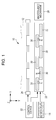
- Fig. 1 is a partial configuration diagram of an ink jet type printing apparatus 10 according to a first embodiment of the invention.
- the printing apparatus 10 of the first embodiment is a liquid ejecting apparatus which ejects ink, which is an exemplification of a liquid, onto a medium (ejection target) 12 such as printing paper and is equipped with a control device 22, a transport mechanism 24, a liquid ejecting unit 26, and a maintenance mechanism 28.
- a liquid container (cartridge) 14 which retains ink of a plurality of colors is mounted in the printing apparatus 10.
- Ink which is retained in the liquid container 14 of the first embodiment is liquid (solvent) ink with suitable high weather resistance for industrial applications.
- the control device 22 collectively controls each of the components of the printing apparatus 10.
- the control device 22 outputs a control signal to each component by generating the control signal in order to control the operation of each of the transport mechanism 24, the liquid ejecting unit 26, and the maintenance mechanism 28.
- the transport mechanism 24 transports the medium 12 in the Y direction under control by the control device 22.
- the liquid ejecting unit 26 ejects ink supplied from the liquid container 14 onto the medium 12 under control by the control device 22.
- the liquid ejecting unit 26 of the first embodiment is a line head in which a plurality of liquid ejecting heads 30 are arranged in the X direction which is orthogonal to the Y direction.
- a plurality of nozzles N are formed on a surface (hereinafter referred to as an "ejection surface" which is to oppose the medium 12 out of each liquid ejecting head 30.
- a desired image is formed on the surface of the medium 12 by each of the liquid ejecting heads 30 ejecting ink onto the medium 12 from each nozzle in parallel with transport of the medium 12 by the transport mechanism 24.
- a direction which is perpendicular to the X-Y horizontal plane (the horizontal plane which is parallel to the surface of the medium 12) is represented below as the Z direction.
- the ejection direction of ink by the liquid ejecting head 30 is equivalent to the Z direction.
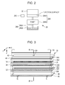
- the maintenance mechanism 28 is utilized in maintenance of the liquid ejecting unit 26.
- the maintenance mechanism 28 of the first embodiment is equipped with a wiper 282, a suction section 284, and a discharge section 286.
- the wiper 282 wipes away ink which is adhered to the ejection surface of each liquid ejecting head 30.
- the suction section 284 is a mechanism which suctions ink inside each liquid ejecting head 30 from each nozzle, and, for example, includes a cap 284A which seals the ejection surface of the liquid ejecting head 30 and a pump 284B which suctions the inside of the cap 284A.
- the discharge section 286 is configured by a tube body 286A and a container 286B which discharge and retain ink which the wiper 282 wipes away or ink which the suction section 284 suctions.
- Each member for example, the wiper 282, the cap 284A, the pipe body 286A, and the container 286B) which is able to come into contact with liquid ink out of the maintenance mechanism 28 are formed by a vulcanized material with solvent resistance (for example, butyl rubber) in order to prevent damage due to adhering of liquid ink.
- the printing apparatus 10 includes the member which is vulcanized (hereinafter referred to as a "vulcanized member") as exemplified above, it is possible to generate gas (outgas) which includes sulfur from the vulcanized member particularly in a high-temperature and high-humidity environment.
- gas gas which includes sulfur from the vulcanized member particularly in a high-temperature and high-humidity environment.
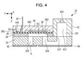
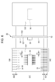
- Fig. 3 is an exploded perspective diagram of one arbitrary liquid ejecting head 30, and Fig. 4 is a sectional diagram (a horizontal cross section on the Y-Z horizontal plane) along line IV-IV in Fig. 3 .
- the liquid ejecting head 30 of the first embodiment has a structure (is a head chip) in which a pressure chamber substrate 34, a vibration plate 36, a sealing plate 44, and a casing 42 are installed on an upper surface at the negative side in the Z direction on a flow path substrate 32, and a nozzle plate 46 and a compliance section 48 are installed on an upper surface at the positive side in the Z direction on the flow path substrate 32.
- Each component of the liquid ejecting head 30 is a member with a substantially flat plate shape with a long dimension in the X direction in outline, and they are fixed to one another utilizing, for example, an adhesive.
- a plurality of the nozzles N are formed on the nozzle plate 46.
- the flow path substrate 32 is a member with a flat plate shape for forming an ink flow path.
- An opening section 322, a supply flow path 324, and a linking flow path 326 are formed on the flow path substrate 32 of the first embodiment.
- the opening section 322 is a through hole with a long dimension in the X direction which links across the plurality of nozzles N
- the supply flow path 324 and the linking flow path 326 are through holes which are formed for each nozzle N.
- the casing 42 is fixed to the surface at the negative side in the Z direction on the flow path substrate 32.
- an accommodating section 422 and an introduction flow path 424 are formed in the casing 42 of the first embodiment.
- the accommodating section 422 is a concave section with an outer form which corresponds to the opening section 322 of the flow path substrate 32
- the introduction flow path 424 is a through hole which links to the accommodating section 422.
- the space which links the opening section 322 of the flow path substrate 32 and the accommodating section 422 of the casing 42 with one another, functions as a liquid retaining chamber (reservoir) SR which retains ink that is supplied from the liquid container 14 via the introduction flow path 424.
- the compliance section 48 in Fig. 4 configures the bottom surface of the liquid retaining chamber SR and suppresses pressure variation in ink inside the liquid retaining chamber SR.
- the pressure chamber substrate 34 in Fig. 3 is a flat plate member in which an opening section 342 is formed for each nozzle N.
- the vibration plate 36 is installed on the surface on the opposite side to the flow path substrate 32 on the pressure chamber substrate 34.
- the vibration plate 36 is a member with a flat plate form which is able to vibrate elastically.
- the vibration plate 36 is configured by, for example, a layer of an elastic film which is formed from an elastic material such as silicon oxide, and an insulation film which is formed from an insulation material such as zirconium oxide. As exemplified in Fig.
- the space which is interposed by the vibration plate 36 and the flow path substrate 32 inside each opening section 342 of the pressure chamber substrate 34 functions as a pressure chamber (cavity) SC in which ink is retained that is supplied from the liquid retaining chamber SR via each supply flow path 324.
- Each pressure chamber SC is linked to the nozzle N via each linking flow path 326 of the flow path substrate 32.
- a piezoelectric element 38 is formed for each nozzle N on the surface (hereinafter referred to as an "installation surface") 362 which is opposite to the pressure chamber substrate 34 on the vibration plate 36.
- a plurality of piezoelectric elements 38 are arranged in the X direction.
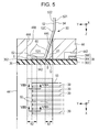
- Fig. 5 is an expanded sectional diagram and a planar diagram of the vicinity of one piezoelectric element 38 within the liquid ejecting head 30. As exemplified in the sectional diagram in Fig.
- each of the plurality of piezoelectric elements 38 contains a first electrode 382 which is formed on a surface of the vibration plate 36, a piezoelectric body layer 384 which is formed on an upper surface of the first electrode 382, and a second electrode 386 which is formed on an upper surface of the piezoelectric body layer 384.
- the first electrode 382 is individually formed for each nozzle N, and the second electrode 386 links across the plurality of nozzles N.
- the vibration plate 36 is equivalent to a specific example of the first board on which a driving element (piezoelectric element 38) is installed.
- the sealing plate 44 in Fig. 4 is a structure that protects each piezoelectric element 38 (for example, prevents water, outside air, and the like coming into contact with the piezoelectric elements 38) and reinforces the mechanical strength of the pressure chamber substrate 34 and the vibration plate 36, and is fixed to the surface of the vibration plate 36 using, for example, an adhesive.
- Each of the plurality of piezoelectric elements 38 is accommodated in a concave section 442 which is formed on the surface opposite to the vibration plate 36 side on the sealing plate 44.
- the sealing plate 44 is equivalent to a specific example of the second board which is installed on a surface of the first board (vibration plate 36) and covers the driving element (piezoelectric element 38).
- the material and the production method of the sealing plate 44 are arbitrary, but, for example, it is possible to form the sealing plate 44 by injection molding of resin material. In addition, it is also possible to form the sealing plate 44 in an anticipated form with high precision by selectively removing the substrate which is configured by single crystal silicon using a semiconductor production technique.
- an opening section 444 is formed on the sealing plate 44 of the first embodiment.
- the opening section 444 is a through hole which extends in the X direction so as to be arranged along the plurality of piezoelectric elements 38, and as understood from Fig. 4 , is positioned at the positive side in the Y direction in planar view (that is, viewed from the Z direction) with respect to each piezoelectric element 38.
- connection terminals 39 are formed in a region (hereinafter referred to as a "mounting region") which is positioned inside the opening section 444 of the sealing plate 44 in planar view on the installation surface 362 of the vibration plate 36.
- Each connection terminal 39 has an electrode for supplying a driving signal for driving the piezoelectric element 38 from outside to the piezoelectric element 38, and extends from the mounting region to the negative side in the Y direction and is connected to the first electrode 382 of each piezoelectric element 38.
- the mounting region is a region which is interposed by a wall surface 446 and a wall surface 448 of the opening section 444 of the sealing plate 44 in planar view on the installation surface 362 of the vibration plate 36.
- the wall surface 446 is an inner (part of the) circumferential surface which extends in the X direction to the negative side in the Y direction
- the wall surface 448 is an inner (part of the) circumferential surface which extends in the X direction to the positive side in the Y direction.
- a flexible wiring board 50 is mounted in the mounting region of the installation surface 362 on the vibration plate 36.
- Fig. 6 is a configuration diagram (front side diagram, side surface diagram, and rear surface diagram) of the wiring board 50.
- the wiring board 50 of the first embodiment is a flexible printed circuit (FPC) which is equipped with a base material 52 and a plurality of wirings 54.
- the base material 52 is a flexible member with a flat plate form (film) which is formed using a resin material such as polyimide, and includes a first surface 521 and a second surface 522 which are positioned opposite one another.
- the plurality of wirings 54 are formed on the first surface 521.
- Fig. 7 is a sectional diagram of the wiring 54 on the wiring board 50.
- each wiring 54 of the first embodiment is configured by layers of a first layer 54A and a second layer 54B.
- the first layer 54A is a conductive layer which is formed on the first surface 521 of the base material 52
- the second layer 54B is a conductive layer which is formed by plating with respect to the first layer 54A.
- the first layer 54A is formed, for example, using a low-resistance conductive material such as copper (Cu), and the second layer 54B protects the first layer 54A by being formed, for example, using a conductive material with high corrosion resistance such as gold (Au) or tin (Sn).
- the wiring board 50 is divided into a first end section 52A, a second end section 52B, and a center section 52C viewed from the direction perpendicular to the first surface 521.
- the first end section 52A is a portion which includes a peripheral edge of one side of the wiring board 50
- the second end section 52B is a portion which includes a peripheral edge of the other side.
- the center section 52C is a portion between the first end section 52A and the second end section 52B.
- the first end section 52A of the wiring board 50 is joined to the installation surface 362 (mounting region) of the vibration plate 36.
- connection terminal 542 a portion inside the first end section 52A out of each wiring 54 on the wiring board 50 functions as a connection terminal 542, and a portion inside the second end section 52B out of each wiring 54 functions as a connection terminal 544.
- a plurality of connection terminals 542 are arranged in a straight-line form along the edge side of the base material 52 in the first edge section 52A, and a plurality of connection terminals 544 are arranged in a straight-line form along the edge side of the base material 52 in the second edge section 52B.
- an IC chip of a driving circuit 56 is mounted on the first surface 521 in the center section 52C of the base material 52.
- the wirings 54 which are formed on the first surface 521 of the base material 52 electrically connect each connection terminal 542 and each connection terminal 544 to the driving circuit 56.
- the second end section 52B is joined to the circuit board on which the control device 22 and a power source device (which is not shown in the diagram) are mounted, and a power source voltage, which is generated by the control signal that is generated by the control device 22, and the power source device, is supplied from the circuit board to each connection terminal 544.
- the driving circuit 56 utilizes the control signal and the power source voltage which are supplied to the connection terminals 544, and generates a driving signal for driving each piezoelectric element 38.
- the driving signals which are generated for each piezoelectric element 38 by the driving circuit 56 are supplied to each connection terminal 542.
- connection terminals 542 are individually formed for each piezoelectric element 38, the total number of connection terminals 542 is significantly greater than the total number of connection terminals 544. Accordingly, the plurality of connection terminals 542 are arranged in the first end section 52A at pitch (period) P1 that is narrower than a pitch P2 at which the plurality of connection terminals 544 are arranged in the second end section 52B (P1 ⁇ P2).
- the first end section 52A of the wiring board 50 is joined to the installation surface 362 of the vibration plate 36 in a state in which the first surface 521 of the first end section 52A of the wiring board 50 is opposed to the installation surface 362 of the vibration plate 36.
- each connection terminal 542 on the first surface 521 of the first end section 52A and each connection terminal 39 on the installation surface 362 are electrically connected by being in contact with one another. That is, each piezoelectric element 38 is electrically connected to the driving circuit 56 via the connection terminal 39 and the wiring 54.
- anisotropic conductive paste ACP
- NCP non-conductive paste
- the wiring board 50 is bent at a boundary B due to being joined on the installation surface 362 such that the boundary B between the first end section 52A and the center section 52C is positioned at the wall surface 446 side (the negative side in the Y direction) of the opening section 444 on the sealing plate 44.
- the center section 52C of the wiring board 50 comes into contact with the wall surface 446 (upper side) of the sealing plate 44 upon being bent so as to be inclined at an obtuse angle with respect to the first end section 52A (or the installation surface 362). Accordingly, as exemplified in Fig.
- a space Q is formed which is enclosed by the installation surface 362 of the vibration plate 36, the wall surface 446 of the sealing plate 44, and the first surface 521 of the wiring board 50 (the center section 52C).
- the space Q is a space with a three-dimensional form in which a central axis is approximate to that of a parallel triangular prism in the X direction with a bottom surface of a triangular shape which is formed by the installation surface 362 of the vibration plate 36, the wall surface 446 of the sealing plate 44, and the first surface 521 of the wiring board 50.
- filling material 60 is formed inside the opening section 444 of the sealing plate 44.
- the filling material 60 is formed using, for example, an epoxy-based adhesive.
- the filling material 60 of the first embodiment includes a portion 61 and a portion 62.
- the portion 61 is a portion of the filling material 60 which is filled inside the space Q. Since the plurality of wirings 54 are formed on the first surface 521 which is equivalent to the inner wall surface of the space Q on the base material 52 of the wiring board 50, the portion 61 of the filling material 60 covers the wiring 54 of the first surface 521 (a portion in the vicinity of the first end section 52A). In detail, the wiring 54 is covered within the region (bent portion) with a bent shape which is bent at the boundary B of the first end section 52A and the center section 52C on the first surface 521 of the base material 52 of the wiring board 50.
- the portion 62 is a portion which is positioned at the positive side in the Y direction inside the opening section 444 of the sealing plate 44, and extends in the X direction (the width direction of the wiring board 50) along a peripheral edge of the first end section 52A of the wiring board 50.
- the portion 62 of the first embodiment partially covers the side surface of the base material 52 and the second surface 522 of the wiring board 50.
- an end surface E in a direction (positive side in the Y direction) in which the wiring 54 extends is also covered by the portion 62 of the filling material 60 out of the wiring 54 (connection terminal 542) which is formed in the first end section 52A.
- Fig. 8A and Fig. 8B are sectional diagrams which are focused on a height H2 of the portion 62 of the filling material 60.
- Fig. 8A is a sectional diagram along line VIIIA-VIIIA in Fig. 5 , and illustrates a section of the portion 62 in the end section of the wiring board 50 in the width direction (X direction).
- Fig. 8B is a sectional diagram along line VIIIB-VIIIB in Fig. 5 , and illustrates a section of the portion 62 in the center section of the wiring board 50 in the width direction.
- the height H2 of the portion 62 with respect to the installation surface 362 of the vibration plate 36 differs according to the position in the width direction of the wiring board 50.
- a height H2a of the portion 62 in both end sections of the wiring board 50 in the width direction is more than a height H2b of the portion 62 in the center section in the width direction (H2a>H2b). That is, the height H2 of the portion 62 of the filling material 60 increases the closer to the end section in the width direction of the wiring board 50.
- Fig. 9 is an explanatory diagram of the wiring board 50 and the filling material 60 which is focused on the heights of the portion 61 and the portion 62 of the filling material 60 with respect to the installation surface 362 of the vibration plate 36.
- the height H2 which is illustrated in Fig. 9 is a maximum height value of the portion 62 (that is, the height H2a of the portion 62 in the end section of the wiring board 50 in the width direction). As understood from Fig.
- the height H1 of the filling material 60 with respect to the installation surface 362 of the portion 61 which is positioned at the first surface 521 side of the wiring board 50 is more than the height H2 of the filling material 60 with respect to the installation surface 362 of the portion 62 which is positioned at the second surface 522 side of the wiring board 50 (H1>H2).
- the height H2 of the portion 62 of the filling material 60 has a dimension to an extent of being slightly more than the second surface 522 of the first end section 52A of the wiring board 50.
- the height H1 of the portion 61 is approximate to the height of the wall surface 446 of the sealing plate 44.
- the height H2 of the portion 62 of the filling material 60 which is positioned at the second surface 522 side of the wiring board 50 is suppressed to a dimension less than the height H1 of the portion 61 which is positioned at the first surface side 521. Accordingly, it is possible to suppress generation of stress which is caused by contraction of the filling material 60 in comparison to a configuration in which the filling material 60 is also formed up to an equal height at the second surface side 522 as at the first surface side 521 of the wiring board 50.
- the filling material 60 is formed such that the height H2 of the portion 62 reduces toward the center of the wiring board 50 in the width direction, the effect described above where stress which is caused by contraction of the filling material 60 is reduced is particularly remarkable in comparison to the configuration in which the portion 62 of the filling material 60 is also formed at an equal height H2a at the center section of the wiring board 50 in the width direction as in each end section.
- the height H1 of the portion 61 of the filling material 60 which is positioned at the first surface 521 side of the wiring board 50 is more than the height H2 of the portion 62 at the second surface side 522. Accordingly, the wiring 54 on the first surface 521 is covered by the filling material 60 across a wide range in comparison to a case in which the height H1 of the portion 61 of the filling material 60 at the first surface side 521 is suppressed to be an equal dimension to the height H2 of the second portion 62. Accordingly, it is possible to suppress the problem such as corrosion of the wiring 54 which is, for example, caused by coming into contact with outside air.
- the wiring 54 of the first embodiment is configured by layers of a first layer 54A and a second layer 54B.
- the first layer 54A is sufficiently adhered to the first surface 521 of the base material 52, but the second layer 54B which is formed by plating has low adhesiveness with the base material 52. Accordingly, although it is possible to protect the first layer 54A using the second layer 54B with high corrosion resistance in a state in which the base material 52 is not bent, when the base material 52 of the wiring board 50 is bent at the boundary B between the first end section 52A and the center section 52C, as exemplified in Fig.
- the second layer 54B is separated from the first surface 521 without deformation of the base material 52 and for the second layer 54B to come into contact with outside air by exposing the second layer 54B from a gap D between the second layer 54B and the first surface 521.
- the first layer 54A is protected from outside air by being maintained in a state in which the first layer 54A is covered by the filling material 60 even in a case where the second layer 54B of the wiring 54 is separated from the first surface 521 caused by bending of the base material 52 in the vicinity of the boundary B.
- the configuration of the first embodiment in which the wiring 54 on the first surface 521 is formed so as to be covered by the filling material 60 (portion 61) across the boundary B is particularly preferable in a configuration in which the wiring 54 of the wiring board 50 is formed in layers of the first layer 54A and the second layer 54B.
- a vulcanized member for example, the wiper 282, the cap 284A, the pipe body 286A, and the container 286B in Fig. 2
- a vulcanized member into which sulfur is mixed in a vulcanizing treatment is utilized from the viewpoint of securing solvent resistance with respect to liquid ink.
- gas which contains sulfur from the vulcanized member.
- sulfur which is generated from the vulcanized member to have a particularly high concentration in circumstances in which the printing apparatus 10 is sealed during transport or the like. Then, as exemplified in Fig.
- the boundary B is positioned at the first end section side 52A at which the plurality of connection terminals 542 are arranged at a narrower pitch P1 than the connection terminals 544 at the second end section 52B (a pitch P2), it is easy for electrical shorts to occur which are caused by generation of copper sulfide in each connection terminal 542 in comparison to each of the connection terminals 544.
- the first layer 54A is maintained in a state of being covered by the filling material 60 even in a case where the second layer 54B of the wiring 54 is separated from the first surface 521 caused by bending of the base material 52 in the vicinity of the boundary B. That is, even in a case where sulfur is generated from the vulcanized member, adherence of sulfur with respect to the first layer 54A of the wiring 54 (thus, generation of copper sulfide) is suppressed. Accordingly, it is advantageous in that it is possible to eliminate the problem such as shorting of each connection terminal 542 which is caused by sulfur which is generated from the vulcanized member.
- the filling material 60 is formed using an epoxy-based adhesive with low permeability with respect to sulfur. Accordingly, the effect described above in which it is possible to prevent defects which are caused by sulfur which is generated from the vulcanized member is particularly remarkable in comparison to a case in which the filling material 60 is formed by, for example, a silicon-based adhesive which is permeable to gas which includes sulfur.
- the configuration of the first embodiment in which the filling material 60 (portion 61) is formed so as to cover the wiring 54 of the first surface 521 is particularly preferable in a configuration in which the printing apparatus 10 is equipped with the vulcanized member (typically, a configuration in which liquid ink is utilized).
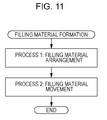
- Fig. 11 is an explanatory diagram of the process in which the filling material 60 is formed.
- the process in Fig. 11 is executed in a state in which the first end section 52A of the wiring board 50 is joined to the installation surface 362 of the vibration plate 36.
- a formation procedure of the filling material 60 of the first embodiment includes Process 1 and Process 2.
- Process 1 is a process in which the filling material 60 is arranged on the installation surface 362 of the vibration plate 36 (inside the opening section 444 of the sealing plate 44).
- Process 2 is a process in which the filling material 60 which is arranged on the installation surface 362 in Process 1 is moved inside the space Q. Specific examples of each process will be given below.
- a liquid filling material 60A is arranged via, for example, a straight needle-form supply pipe in the vicinity of one end section (the end section at the negative side in the X direction in the exemplification in Fig. 12 ) of the space Q on the installation surface 362.
- the filling material 60A is arranged so as to block the one end section of the space Q.
- the filling material 60A is caused to enter into the space Q due to capillary force of the space Q by being maintained in the above state.
- the portion 61 of the filling material 60 is formed by curing the filling material 60A at a stage of reaching the entirety of the space Q.
- the portion 62 of the filling material 60 is formed by the filling material 60A, which is arranged on the installation surface 362 in Process 1, being advanced along the peripheral edge of the wiring board 50 due to capillary force.
- the method for causing the filling material 60A to enter into the space Q is arbitrary.
- a method in which the filling material 60A is caused to enter into the space Q by reducing the viscosity using heat, and a method in which the filling material 60A is caused to enter into the space Q by inclining the installation surface 362 may be used.
- the liquid filling material 60A is arranged via, for example, a straight needle-form supply pipe in the vicinity of both end sections of the space Q on the installation surface 362.
- the usage amount of liquid droplets is adjusted such that the filling material 60A does not form a meniscus at each end of the space Q.
- the filling material 60A is caused to move into the space Q from both sides by, for example, executing vacuuming.
- the filling material 60A is cured in a stage of reaching the entirety of the space Q.
- the portion 62 of the filling material 60 is formed by the filling material 60A, which is arranged at both sides of the space Q in Process 1, being advanced near to the center from both sides of the wiring board 50 due to capillary force.
- the filling material 60A is exemplified separately to the adhesive for joining the wiring board 50, but it is also possible to utilize an adhesive for joining the wiring board 50 to the installation surface 362 in the formation of the filling material 60.
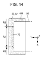
- Fig. 14 is an expanded planar diagram of the inside of the opening section 444 of the sealing plate 44 in the second embodiment.
- an adhesive for example, an epoxy-based adhesive
- an adhesive 70 for joining the wiring board 50 to the installation surface 362 of the vibration plate 36 protrudes out of the region outside from between the first surface 521 of the wiring board 50 and the installation surface 362.
- a portion of the adhesive 70 which protrudes out from between the first surface 521 and the installation surface 362 covers the end surface E of each wiring 54 and the second surface 522 of the base material 52 by being distributed across a range RA in the width direction of the wiring board 50.
- protrusion of the adhesive 70 does not occur in a range RB outside the range RA in the width direction of the wiring board 50. Accordingly, the end surface E of each wiring 54 on the wiring board 50 and the second surface 522 of the base material 52 in the range RB are not covered by the adhesive 70.
- the portion 62 of the filling material 60 of the second embodiment is only formed on the end surface E within each range RB and not the range RA. That is, the portion 62 is formed so as to cover a portion of the wiring 54 on the wiring board 50 which is not covered by the adhesive 70, and the portion 62 is not formed within the range RA in which each wiring 54 is covered by the adhesive 70.
- the second embodiment since the portion 62 of the filling material 60 is formed so as to cover the portion of the wiring 54 on the wiring board 50 which is not covered by the adhesive 70, the usage amount of the liquid-form filling material 60A necessary in formation of the portion 62 is reduced in comparison to the portion 62 of the filling material 60 which links across the entire region of the wiring board 50 in the width direction. Accordingly, it is advantageous in that production costs of the liquid ejecting head 30 are reduced.
- Fig. 15 is an expanded sectional diagram and a planar diagram of the vicinity of one piezoelectric element 38 within the liquid ejecting head 30 of the third embodiment.
- the first end section 52A of the wiring board 50 is joined to the installation surface 362 on the vibration plate 36 using the adhesive 70.
- anisotropic conductive paste (ACP) or non-conductive paste (NCP) is preferably utilized as the adhesive 70.
- the adhesive 70 is filled into the space Q by protruding to the negative side (the wall surface 446 side of the sealing plate 44) in the Y direction from between the first end section 52A and the installation surface 362.
- the portion of the adhesive 70 which protrudes out to the negative side in the Y direction from between the wiring board 50 and the vibration plate 36 covers the first surface 521 of the wiring board 50 by being distributed across substantially the entire range (for example, a range including both the range RA and the range RB in Fig. 14 ) in the width direction on the wiring board 50. That is, in the third embodiment, the filling material is formed so as to cover the wiring 54 (that is, cover the wiring 54 of the bent portion at the boundary B on the wiring board 50) across the boundary B between the wall surface 446 of the sealing plate 44 and the first surface 521 of the wiring board 50 using the adhesive 70 in order to join the wiring board 50 and the vibration plate 36.
- the portion of the adhesive 70 which protrudes out to the positive side (the wall surface 448 side of the sealing plate 44) in the Y direction from between the wiring board 50 and the vibration plate 36 covers the end surface E of each wiring 54 of the wiring board 50.
- the adhesive 70 for joining the wiring board 50 and the vibration plate 36 is applied as the filling material, the amount of resin material formed inside the opening section 444 of the sealing plate 44 is reduced in comparison to the first embodiment in which the filling material 60 is formed separately from the adhesive. Accordingly, it is possible to suppress stress caused by contraction of the filling material inside the opening section 44.
- the filling material is formed in the process in which the wiring board 50 is joined to the vibration plate 36, it is advantageous in that the production process is simplified (thus, production costs are reduced) in comparison to the first embodiment in which the filling material 60 is formed in an individual process to the joining of the wiring board 50 and the vibration plate 36.
- the liquid-form adhesive 70A is coated in the mounting region inside the opening section 444 of the sealing plate 44 on the installation surface 362 on the vibration plate 36.
- the adhesive 70A is coated at a position of a substantially central point between the wall surface 446 and the wall surface 448.
- the first side section 52A of the wiring board 50 is bent at the boundary B with respect to the center section 52C.
- a jig 80 (mounting tool) for mounting on the wiring board 50 is moved to installation surface 362 side in a state in which a pressing surface 82 of the jig 80 comes into contact with the second surface 522 of the first end section 52A, and the adhesive 70A is caused to flow and is diffused in a direction parallel to the installation surface 362 due to the adhesive 70A being pressed by the first surface 521 of the first end section 52A.
- the adhesive 70 in Fig. 15 is formed by curing the adhesive 70A in a state in which the first surface 521 is adhered to the installation surface 362.
- the adhesive 70A is coated at a position at the wall surface 446 side of the sealing plate 44 in comparison to Production Example B1 on the installation surface 362 of the vibration plate 36.
- the adhesive 70A is coated at a position a prescribed amount closer to the wall surface 446 with respect to the substantially central point between the wall surface 446 and the wall surface 448.
- the first end section 52A of the wiring board 50 is bent substantially perpendicularly with respect to the center section 52C, but in Production Example B3, as exemplified in Fig. 18 , the first end section 52A of the wiring board 50 is bent at the boundary B so as to form an obtuse angle with respect to the first end section 52A and the center section 52C.
- the jig 80 which comes into contact with the second surface 522 is caused to approach the wiring board 50 and the installation surface 362 in a state in which the first end section 52A is inclined with respect to the installation surface 362 of the vibration plate 36 (that is, intersects at a non-perpendicular angle).
- the adhesive 70A which is coated on the installation surface 362 is squeezed out at the wall surface 446 side of the sealing plate 44 by being pressed by the first surface 521 of the first end section 52. Meanwhile, the first end section 52A of the wiring board 50 approaches in a state of being substantially orthogonal to the center section 52C by coming into contact with and approaching the installation surface 362.
- the adhesive 70 in Fig. 15 is formed by curing the adhesive 70A in a state in which the first surface 521 is adhered to the installation surface 362.
- Production Example B3 in the same manner as in Production Example B2, it is possible to effectively aggregate the adhesive 70A at the wall surface 446 side.
- the adhesive 70A may be positioned the same as in Production Example B1 or B2.
- the adhesive 70A is coated on the installation surface 362 of the vibration plate 36, but it is also possible to install the anisotropic conductive paste (ACP) or an anisotropic conductive film (ACF) in advance on the first surface 521 of the first end section 52A of the wiring board 50 as the adhesive 70A, and form the adhesive 70 by pressing the first end section 52A on the installation surface 362 using the jig 80.
- ACP anisotropic conductive paste
- ACF anisotropic conductive film
- Fig. 19 is an expanded sectional diagram and a planar diagram of the vicinity of one piezoelectric element 38 within the liquid ejecting head 30 of the fourth embodiment.
- a coating material 75 is formed (for example, potted) in addition to the adhesive 70, which is formed in the same manner as the third embodiment.
- the coating material 75 is formed using, for example, an epoxy-based adhesive which has low permeability with respect to gas such as sulfur, and extends along the width direction (X direction) of the wiring board 50.
- the coating material 75 which is exemplified in Fig.
- the coating material 75 is formed in addition to the adhesive 70, it is advantageous in that it is possible to effectively protect the end surface E and suppress corrosion and the like using the coating material 75 even in a case in which, for example, the end surface E of each wiring 54 on the wiring board 50 is exposed from the adhesive 70.
- the adhesive 70 is not formed on the surface of the second surface 522 of the first end section 52A on the wiring board 50
- the adhesive 70 covers the second surface 522 it is advantageous in that it is possible to effectively protect the end section E of each wiring 54 without the need to form the coating material 75 which is exemplified, for example, in the fourth embodiment.
- the adhesive 70 covers the second surface 522
- the adhesive 70 is not formed on the surface of the second surface 522, it is advantageous in that it is possible to prevent adherence of the adhesive 70 with respect to the jig 80, even in a case in which, for example, the adhesive 70A is excessively coated.
- the filling material which is formed using the adhesive 70 in the third embodiment and the fourth embodiment to satisfy the condition (H2a>H2b, H1>H2) exemplified in the first embodiment, but it is also possible to adopt a configuration in which the condition is not satisfied.
- the filling material which covers each wiring 54 is formed between the installation surface 362 on the vibration plate 36 and the wall surface 446 of the sealing plate 44, the form of the space Q is not an essential condition.
- the filling material 60 which includes the portion 61 at the first surface 521 side (the inside of the space Q) and the portion 62 at the second surface 522 side (the outside of the space Q) of the wiring board 50 is exemplified, but it is also possible to omit the portion 62, and configure the filling material 60 with only the portion 61 which is filled inside the space Q.
- the condition described above in which the height H1 of the portion 61 of the filling material 60 at the first surface side 521 is more than the height H2 of the portion 62 at the second surface 522 side includes a case in which the height H2 of the portion 62 is a prescribed positive number as well as a case in which the height H2 is zero (a configuration in which the portion 62 is omitted).
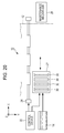
- a line head is exemplified where the plurality of liquid ejecting heads 30 are arranged in the X direction which is orthogonal to the Y direction in which the medium 12 is transported, but it is possible to also apply the invention to a serial head.
- each of the liquid ejecting heads 30 eject ink onto the medium 12 while a carriage 27, on which the plurality of liquid ejecting heads 30 according to each of the aspects described above are mounted, moves back and forth in the X direction under control by the control device 22.
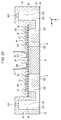
- the liquid ejecting head 30 is exemplified in which the plurality of nozzles N are arranged in one row, but as exemplified in Fig. 21 , it is also possible to realize the liquid ejecting head in which ink is ejected from two rows of the nozzles N by arranging the configuration substantially line symmetrically in the same manner as each of the aspects described above.
- ink is ejected from two rows of the nozzles N by arranging the configuration substantially line symmetrically in the same manner as each of the aspects described above.
- the components (driving elements) which vary the pressure inside the pressure chamber SC are not limited to the piezoelectric elements 38 exemplified in each embodiment described above.
- an oscillator such as an electrostatic actuator as the driving element.
- the driving elements are not limited to components which impart mechanic vibration to the pressure chambers SC.
- a heat generating element which varies the pressure by generating bubbles inside the pressure chambers SC by heating, as the driving element.
- the driving elements are comprehensively expressed as components for ejecting liquid (typically elements which apply pressure inside the pressure chambers SC), and neither the operating method (piezo method/thermal method) nor the detailed configuration are relevant.
- the printing apparatus 10 which is exemplified in each of the aspects above in various devices, other than a device which is specialized for printing, such as a facsimile apparatus or a copy machine.
- the applications of the liquid ejecting apparatus of the invention are not limited to printing.
- a liquid ejecting apparatus which ejects color liquid is utilized as a manufacturing apparatus which forms a color filter of a liquid crystal display apparatus.
- a liquid ejecting apparatus which ejects a conductive material solution is utilized as a manufacturing apparatus which forms an electrode and a wiring of a wiring substrate.
Landscapes
- Particle Formation And Scattering Control In Inkjet Printers (AREA)
- Engineering & Computer Science (AREA)
- Manufacturing & Machinery (AREA)
- Ink Jet (AREA)
Description
- This application claims priority to Japanese Patent Application No.
2014-218559 filed on October 27, 2014 2014-218559 - The present invention relates to a technique for ejecting liquid such as ink.
- Various structures of a liquid ejecting head which ejects liquid such as ink from a nozzle are proposed in the related art. For example,
JP-A-2013-202857 - The filling material is filled into the opening section of the protective board to the extent of a sufficient filling amount which is equal to the height of the filling material at one side and another side of the wiring board. In the configuration above, for example, it is possible that stress is generated in each component of the liquid ejecting head due to contraction of the filling material during curing, and as a result, that deformation, peeling, or the like is caused in each component. Meanwhile, if the filling material is omitted, the problem of stress which is caused by contraction of the filling material is eliminated, but there is the problem such as corrosion of the wiring occurring caused by the wiring on the wiring board coming into contact with outside air due to exposure. For example, when utilizing a vulcanized material (for example, butyl rubber) in a liquid ejecting apparatus which ejects liquid ink, it is possible for the wiring to be corroded by gas (outgas) being generated which contains sulfur in a high-temperature and high-humidity environment.
- An advantage of some aspects of the invention is to suppress stress which is caused by compression of filling material which covers a wiring on a wiring board.
- According to a preferred aspect (Aspect 1) of the invention, there is provided a liquid ejecting head including: a first board on which a driving element for ejecting liquid is installed; a second board which is installed on the surface of the first board and covers the driving element; a wiring board that includes a first surface on which a wiring, where a driving signal is supplied to the driving element, is formed and a second surface that is at the opposite side to the first surface, and where the first surface of a first end section is joined to the surface of the first board; and a filling material which covers the wiring by being formed at least between the first surface and a wall surface of the second board, in which the height of the filling material with respect to the surface of the first board is high at the first surface side in comparison to the second surface side. In
Aspect 1, the height of the filling material with respect to the surface of the first board is lower at the second surface side in comparison to the first surface side of the wiring board. Accordingly, it is possible to suppress stress which is caused by contraction of the filling material in comparison to a configuration in which the filling material is also formed up to an equal height at the second surface side to at the first surface side of the wiring board. Meanwhile, the height of the filling material with respect to the surface of the first board is higher at the first surface side in comparison to the second surface side of the wiring board. Accordingly, the wiring on the first surface is covered by the filling material across a wide range in comparison to a case in which the height of the filling material at the first surface side of the wiring board is suppressed to be an equal height to the second surface side. Accordingly, it is possible to suppress the problem such as corrosion of a wiring which is, for example, caused by adhesion with outside air or water. Here, the filling material covers the wiring between the first surface and the wall surface of the second board if the filling material covers the wiring across a boundary of a bend in a case where a portion which is joined to the surface of the first board out of the wiring board is distinguished from a portion which is not joined to the surface of the first board due to the bend of the wiring board. - In the liquid ejecting head of a preferred example (Aspect 2) according to
Aspect 1, the filling material may be filled inside a space which is enclosed by a surface of the first board, a wall surface of the second board, and the first surface of a portion which is bent with respect to the first end section out of the wiring board. InAspect 2, it is advantageous in that it is possible to effectively utilize a space which is enclosed by the surface of the first board, the wall surface of the second board, and the first surface of the wiring board in formation of the filling material. - In the liquid ejecting head of a preferred example (Aspect 3) according to
Aspect 1 orAspect 2, the height of the filling material at the second surface side with respect to the surface of the first board may be low in the center section of the wiring board in a width direction in comparison to the end section of the wiring board in the width direction. In Aspect 3, since the height of the filling material at the second surface side of the wiring board is low at the center section in comparison to the end section of the wiring board in the width direction, the effect described above where stress, which is caused by contraction of the filling material, is reduced is particularly remarkable in comparison to the configuration in which the filling material is also formed at an equal height at the center section of the wiring board in the width direction to the height at each end section. - According to another preferred aspect(Aspect 4) of the invention, there is provided a liquid ejecting head including: a first board on which a driving element for ejecting liquid is installed; a second board which is installed on the surface of the first board and covers the driving element; a wiring board that includes a first surface on which a wiring, where a driving signal is supplied to the driving element, is formed and a second surface that is at the opposite side to the first surface, and where the first surface of a first end section is joined to the surface of the first board; and a filling material which covers a bent portion of the wiring board by being formed at least between the first surface and a wall surface of the second board using an adhesive in order to join the wiring board and the first board. In
Aspect 4, since the filling material is formed so as to cover the wiring between the first surface and the wall surface of the second board (that is, an adhesive is applied as the filling material) using an adhesive in order to join the wiring board and the first board, the amount of filling material formed on the surface of the first board is reduced in comparison to the configuration in which the adhesive for the joint between the wiring board and the first board is formed separately to the filling material. Accordingly, it is possible to suppress stress caused by contraction of the filling material. - In the liquid ejecting head of a preferred example (Aspect 5) according to any one of
Aspects 1 to 4, the wiring on the wiring board may include a first layer and second layer which is formed by plating with respect to the first layer. In Aspect 5, since the second layer is formed by plating with respect to the first layer, it is possible to suppress the problem such as corrosion of the first layer even if the wiring on the first surface of the wiring board is not covered by the filling material across the entire range. - In the liquid ejecting head of a preferred example (Aspect 6) according to any one of
Aspects 1 to 5, the filling material may be formed by an epoxy-based adhesive. In Aspect 6, since the filling material is formed by an epoxy-based adhesive, it is advantageous in that it is possible to suppress the problem such as corrosion of the wiring due to coming into contact with gas which has passed through the filling material in comparison to the configuration in which the filling material is formed, for example, by a silicone-based adhesive with high permeability with respect to gas of sulfur or the like. - In the liquid ejecting head of a preferred example (Aspect 7) according to any one of
Aspects 1 to 6, the wiring board may include the first end section in which a plurality of connection terminals are arranged at a first pitch and a second end section in which a plurality of connection terminals are arranged at a second pitch which is wider than the first pitch, and the filling material may cover the first end section. For example, the effect of corrosion and the like which is caused by coming into contact with outside air particularly becomes a problem (for example, a short between wirings) based on a configuration in which multiple wirings are densely arranged at a narrow pitch. In the invention, as described above, since corrosion of the wiring is effectively prevented by the wiring on the first surface of the wiring board being covered by the filling material across a wide range, it is possible to suppress a problem such as corrosion of each wiring even in Aspect 7 in which a plurality of wirings are arranged at a narrow pitch in the first end section. - In the liquid ejecting head of a preferred example (Aspect 8) according to any one of
Aspects 1 to 7, the filling material may cover an end surface of the wiring board in a direction in which the wiring extends. In Aspect 8, since the end surface in the direction in which the wiring extends is also covered by the filling material, the effect described above in which it is possible to suppress the problem such as corrosion of the wiring is particularly remarkable. - In the liquid ejecting head of a preferred example (Aspect 9) according to any one of
Aspects 1 to 8, the first end section of the wiring board may be joined to an installation surface using the adhesive, and the filling material may cover a portion of the wiring on the wiring board, the position not being covered by the adhesive. In Aspect 9, since the filling material is formed so as to cover a portion of the wiring on the wiring board, the position not being covered by the adhesive of a joint of the wiring board, it is advantageous in that it is possible to reduce the usage amount of filling material. - According to still another preferred aspect (Aspect 10) of the invention, there is provided a liquid ejecting apparatus including the liquid ejecting head according to each aspect described above. A printing apparatus which ejects ink is a preferred example of the liquid ejecting apparatus, but the applications of the liquid ejecting apparatus according to the invention are not limited thereto.
- The liquid ejecting apparatus of a preferred example (Aspect 11) according to
Aspect 10 may further include a vulcanized member. A member to which solvent resistance is added by vulcanization is preferably utilized at a location at which liquid ink comes in contact. Meanwhile, although it is possible for gas to be generated which includes sulfur from the member which is vulcanized, according to the invention, it is advantageous in that it is possible to prevent corrosion and the like of the wiring which is caused by coming into contact with gas by covering the wiring on the first surface of the wiring board across a wide range using the filling material. - According to still another preferred aspect (Aspect 12) of the invention, there is provided a production method of a liquid ejecting head which includes a first board on which a driving element for ejecting liquid is installed, a second board which is installed on the surface of the first board and covers the driving element, and a wiring board that includes a first surface on which a wiring, where a driving signal is supplied to the driving element, is formed and a second surface that is at the opposite side to the first surface, and where the first surface of a first end section is joined to the surface of the first board, the method including: arranging a filling material on a surface of the first board; and moving the filling material inside a space which is enclosed by a surface of the first board, a wall surface of the second board, and the first surface of the wiring board. According to the method above, it is possible to simply form the filling material within a space which is enclosed by the surface of the first board, the wall surface of the second board, and the first surface of the wiring board by causing the filling material which is arranged on the surface of the first board to move.
- According to still another preferred aspect (Aspect 13) of the invention, there is provided a production method of a liquid ejecting head which includes a first board on which a driving element for ejecting liquid is installed, a second board which is installed on the surface of the first board and covers the driving element, and a wiring board that includes a first surface on which a wiring, where a driving signal is supplied to the driving element, is formed and a second surface that is at the opposite side to the first surface, and where the first surface of a first end section is joined to the surface of the first board, the method including: joining the wiring board and the first board using an adhesive; and covering a bent portion of the wiring board between the first surface and a wall surface of the second board with the adhesive. According to the method above, it is possible to form the filling material which covers a bent portion of the wiring board between the first surface and the wall surface of the second board using an adhesive in order to join the wiring board and the first board.
- Embodiments of the invention will now be described by way of example only with reference to the accompanying drawings, wherein like numbers reference like elements.
-
Fig. 1 is a configuration diagram of a printing apparatus according to a first embodiment of the invention. -
Fig. 2 is an explanatory diagram of a maintenance mechanism of the printing apparatus. -
Fig. 3 is an exploded perspective diagram of a liquid ejecting head. -
Fig. 4 is a sectional diagram of the liquid ejecting head (a sectional diagram along line IV-IV inFig. 3 ). -
Fig. 5 is an explanatory diagram which is focused on the installation of a wiring board. -
Fig. 6 is a configuration diagram of the wiring board. -
Fig. 7 is a sectional diagram of a wiring on the wiring board. -
Fig. 8A and Fig. 8B are explanatory diagrams of a filling material. -
Fig. 9 is an explanatory diagram of the filling material. -
Fig. 10 is an explanatory diagram which relates to peeling of the second layer of the wiring. -
Fig. 11 is a process diagram of a method in which the filling material is formed. -
Fig. 12 is an explanatory diagram of a method (Production Example A1) in which the filling material is formed. -
Fig. 13 is an explanatory diagram of a method (Production Example A2) in which the filling material is formed. -
Fig. 14 is an explanatory diagram of the filling material in a second embodiment. -
Fig. 15 is an explanatory diagram of a liquid ejecting head according to a third embodiment. -
Fig. 16 is an explanatory diagram of a method (Production Example B1) in which the wiring board is mounted in the third embodiment. -
Fig. 17 is an explanatory diagram of a method (Production Example B2) in which the wiring board is mounted in the third embodiment. -
Fig. 18 is an explanatory diagram of a method (Production Example B3) in which the wiring board is mounted in the third embodiment. -
Fig. 19 is a configuration diagram of a liquid ejecting head according to a fourth embodiment. -
Fig. 20 is a configuration diagram of a printing apparatus according to a modification example. -
Fig. 21 is a sectional diagram of a liquid ejecting head according to a modification example. -
Fig. 1 is a partial configuration diagram of an ink jettype printing apparatus 10 according to a first embodiment of the invention. Theprinting apparatus 10 of the first embodiment is a liquid ejecting apparatus which ejects ink, which is an exemplification of a liquid, onto a medium (ejection target) 12 such as printing paper and is equipped with acontrol device 22, atransport mechanism 24, aliquid ejecting unit 26, and amaintenance mechanism 28. As exemplified inFig. 1 , a liquid container (cartridge) 14 which retains ink of a plurality of colors is mounted in theprinting apparatus 10. Ink which is retained in theliquid container 14 of the first embodiment is liquid (solvent) ink with suitable high weather resistance for industrial applications. - The
control device 22 collectively controls each of the components of theprinting apparatus 10. In detail, thecontrol device 22 outputs a control signal to each component by generating the control signal in order to control the operation of each of thetransport mechanism 24, theliquid ejecting unit 26, and themaintenance mechanism 28. Thetransport mechanism 24 transports the medium 12 in the Y direction under control by thecontrol device 22. Theliquid ejecting unit 26 ejects ink supplied from theliquid container 14 onto the medium 12 under control by thecontrol device 22. Theliquid ejecting unit 26 of the first embodiment is a line head in which a plurality of liquid ejecting heads 30 are arranged in the X direction which is orthogonal to the Y direction. A plurality of nozzles N are formed on a surface (hereinafter referred to as an "ejection surface" which is to oppose the medium 12 out of each liquid ejectinghead 30. A desired image is formed on the surface of the medium 12 by each of the liquid ejecting heads 30 ejecting ink onto the medium 12 from each nozzle in parallel with transport of the medium 12 by thetransport mechanism 24. Here, a direction which is perpendicular to the X-Y horizontal plane (the horizontal plane which is parallel to the surface of the medium 12) is represented below as the Z direction. The ejection direction of ink by theliquid ejecting head 30 is equivalent to the Z direction. - The
maintenance mechanism 28 is utilized in maintenance of theliquid ejecting unit 26. As exemplified inFig. 2 , themaintenance mechanism 28 of the first embodiment is equipped with awiper 282, asuction section 284, and adischarge section 286. Thewiper 282 wipes away ink which is adhered to the ejection surface of each liquid ejectinghead 30. Thesuction section 284 is a mechanism which suctions ink inside each liquid ejectinghead 30 from each nozzle, and, for example, includes acap 284A which seals the ejection surface of theliquid ejecting head 30 and apump 284B which suctions the inside of thecap 284A. Thedischarge section 286 is configured by atube body 286A and acontainer 286B which discharge and retain ink which thewiper 282 wipes away or ink which thesuction section 284 suctions. Each member (for example, thewiper 282, thecap 284A, thepipe body 286A, and thecontainer 286B) which is able to come into contact with liquid ink out of themaintenance mechanism 28 are formed by a vulcanized material with solvent resistance (for example, butyl rubber) in order to prevent damage due to adhering of liquid ink. In a configuration in which theprinting apparatus 10 includes the member which is vulcanized (hereinafter referred to as a "vulcanized member") as exemplified above, it is possible to generate gas (outgas) which includes sulfur from the vulcanized member particularly in a high-temperature and high-humidity environment. -
Fig. 3 is an exploded perspective diagram of one arbitraryliquid ejecting head 30, andFig. 4 is a sectional diagram (a horizontal cross section on the Y-Z horizontal plane) along line IV-IV inFig. 3 . As exemplified inFig. 3 andFig. 4 , theliquid ejecting head 30 of the first embodiment has a structure (is a head chip) in which apressure chamber substrate 34, avibration plate 36, a sealingplate 44, and acasing 42 are installed on an upper surface at the negative side in the Z direction on aflow path substrate 32, and anozzle plate 46 and acompliance section 48 are installed on an upper surface at the positive side in the Z direction on theflow path substrate 32. Each component of theliquid ejecting head 30 is a member with a substantially flat plate shape with a long dimension in the X direction in outline, and they are fixed to one another utilizing, for example, an adhesive. A plurality of the nozzles N are formed on thenozzle plate 46. - The
flow path substrate 32 is a member with a flat plate shape for forming an ink flow path. Anopening section 322, asupply flow path 324, and a linkingflow path 326 are formed on theflow path substrate 32 of the first embodiment. As exemplified inFig. 3 , theopening section 322 is a through hole with a long dimension in the X direction which links across the plurality of nozzles N, and thesupply flow path 324 and the linkingflow path 326 are through holes which are formed for each nozzle N. - The
casing 42 is fixed to the surface at the negative side in the Z direction on theflow path substrate 32. As exemplified inFig. 4 , anaccommodating section 422 and anintroduction flow path 424 are formed in thecasing 42 of the first embodiment. Theaccommodating section 422 is a concave section with an outer form which corresponds to theopening section 322 of theflow path substrate 32, and theintroduction flow path 424 is a through hole which links to theaccommodating section 422. As exemplified inFig. 4 , the space, which links theopening section 322 of theflow path substrate 32 and theaccommodating section 422 of thecasing 42 with one another, functions as a liquid retaining chamber (reservoir) SR which retains ink that is supplied from theliquid container 14 via theintroduction flow path 424. Thecompliance section 48 inFig. 4 configures the bottom surface of the liquid retaining chamber SR and suppresses pressure variation in ink inside the liquid retaining chamber SR. - The
pressure chamber substrate 34 inFig. 3 is a flat plate member in which anopening section 342 is formed for each nozzle N. Thevibration plate 36 is installed on the surface on the opposite side to theflow path substrate 32 on thepressure chamber substrate 34. Thevibration plate 36 is a member with a flat plate form which is able to vibrate elastically. Thevibration plate 36 is configured by, for example, a layer of an elastic film which is formed from an elastic material such as silicon oxide, and an insulation film which is formed from an insulation material such as zirconium oxide. As exemplified inFig. 4 , the space which is interposed by thevibration plate 36 and theflow path substrate 32 inside eachopening section 342 of thepressure chamber substrate 34 functions as a pressure chamber (cavity) SC in which ink is retained that is supplied from the liquid retaining chamber SR via eachsupply flow path 324. Each pressure chamber SC is linked to the nozzle N via each linkingflow path 326 of theflow path substrate 32. - A
piezoelectric element 38 is formed for each nozzle N on the surface (hereinafter referred to as an "installation surface") 362 which is opposite to thepressure chamber substrate 34 on thevibration plate 36. As exemplified inFig. 3 , a plurality ofpiezoelectric elements 38 are arranged in the X direction.Fig. 5 is an expanded sectional diagram and a planar diagram of the vicinity of onepiezoelectric element 38 within theliquid ejecting head 30. As exemplified in the sectional diagram inFig. 5 , each of the plurality ofpiezoelectric elements 38 contains afirst electrode 382 which is formed on a surface of thevibration plate 36, apiezoelectric body layer 384 which is formed on an upper surface of thefirst electrode 382, and asecond electrode 386 which is formed on an upper surface of thepiezoelectric body layer 384. Thefirst electrode 382 is individually formed for each nozzle N, and thesecond electrode 386 links across the plurality of nozzles N. However, it is also possible to form thefirst electrode 382 across the plurality of nozzles N, and individually form thesecond electrode 386 for each nozzle N. As understood from the above explanation, thevibration plate 36 is equivalent to a specific example of the first board on which a driving element (piezoelectric element 38) is installed. - The sealing
plate 44 inFig. 4 is a structure that protects each piezoelectric element 38 (for example, prevents water, outside air, and the like coming into contact with the piezoelectric elements 38) and reinforces the mechanical strength of thepressure chamber substrate 34 and thevibration plate 36, and is fixed to the surface of thevibration plate 36 using, for example, an adhesive. Each of the plurality ofpiezoelectric elements 38 is accommodated in aconcave section 442 which is formed on the surface opposite to thevibration plate 36 side on the sealingplate 44. As understood from the above explanation, the sealingplate 44 is equivalent to a specific example of the second board which is installed on a surface of the first board (vibration plate 36) and covers the driving element (piezoelectric element 38). The material and the production method of the sealingplate 44 are arbitrary, but, for example, it is possible to form the sealingplate 44 by injection molding of resin material. In addition, it is also possible to form the sealingplate 44 in an anticipated form with high precision by selectively removing the substrate which is configured by single crystal silicon using a semiconductor production technique. - As exemplified in
Fig. 3 , anopening section 444 is formed on the sealingplate 44 of the first embodiment. Theopening section 444 is a through hole which extends in the X direction so as to be arranged along the plurality ofpiezoelectric elements 38, and as understood fromFig. 4 , is positioned at the positive side in the Y direction in planar view (that is, viewed from the Z direction) with respect to eachpiezoelectric element 38. - As exemplified in
Fig. 5 , a plurality ofconnection terminals 39 are formed in a region (hereinafter referred to as a "mounting region") which is positioned inside theopening section 444 of the sealingplate 44 in planar view on theinstallation surface 362 of thevibration plate 36. Eachconnection terminal 39 has an electrode for supplying a driving signal for driving thepiezoelectric element 38 from outside to thepiezoelectric element 38, and extends from the mounting region to the negative side in the Y direction and is connected to thefirst electrode 382 of eachpiezoelectric element 38. The mounting region is a region which is interposed by awall surface 446 and awall surface 448 of theopening section 444 of the sealingplate 44 in planar view on theinstallation surface 362 of thevibration plate 36. Thewall surface 446 is an inner (part of the) circumferential surface which extends in the X direction to the negative side in the Y direction, and thewall surface 448 is an inner (part of the) circumferential surface which extends in the X direction to the positive side in the Y direction. As exemplified inFig. 4 and5 , aflexible wiring board 50 is mounted in the mounting region of theinstallation surface 362 on thevibration plate 36. -
Fig. 6 is a configuration diagram (front side diagram, side surface diagram, and rear surface diagram) of thewiring board 50. As exemplified inFig. 6 , thewiring board 50 of the first embodiment is a flexible printed circuit (FPC) which is equipped with abase material 52 and a plurality ofwirings 54. Thebase material 52 is a flexible member with a flat plate form (film) which is formed using a resin material such as polyimide, and includes afirst surface 521 and asecond surface 522 which are positioned opposite one another. The plurality ofwirings 54 are formed on thefirst surface 521. -
Fig. 7 is a sectional diagram of thewiring 54 on thewiring board 50. As exemplified inFig. 7 , eachwiring 54 of the first embodiment is configured by layers of afirst layer 54A and asecond layer 54B. Thefirst layer 54A is a conductive layer which is formed on thefirst surface 521 of thebase material 52, and thesecond layer 54B is a conductive layer which is formed by plating with respect to thefirst layer 54A. Thefirst layer 54A is formed, for example, using a low-resistance conductive material such as copper (Cu), and thesecond layer 54B protects thefirst layer 54A by being formed, for example, using a conductive material with high corrosion resistance such as gold (Au) or tin (Sn). - As exemplified in
Fig. 6 , thewiring board 50 is divided into afirst end section 52A, asecond end section 52B, and acenter section 52C viewed from the direction perpendicular to thefirst surface 521. Thefirst end section 52A is a portion which includes a peripheral edge of one side of thewiring board 50, and thesecond end section 52B is a portion which includes a peripheral edge of the other side. Thecenter section 52C is a portion between thefirst end section 52A and thesecond end section 52B. As exemplified inFig. 5 , thefirst end section 52A of thewiring board 50 is joined to the installation surface 362 (mounting region) of thevibration plate 36. - As exemplified in
Fig. 6 , a portion inside thefirst end section 52A out of eachwiring 54 on thewiring board 50 functions as aconnection terminal 542, and a portion inside thesecond end section 52B out of each wiring 54 functions as aconnection terminal 544. A plurality ofconnection terminals 542 are arranged in a straight-line form along the edge side of thebase material 52 in thefirst edge section 52A, and a plurality ofconnection terminals 544 are arranged in a straight-line form along the edge side of thebase material 52 in thesecond edge section 52B. In addition, an IC chip of a drivingcircuit 56 is mounted on thefirst surface 521 in thecenter section 52C of thebase material 52. Thewirings 54 which are formed on thefirst surface 521 of thebase material 52 electrically connect eachconnection terminal 542 and eachconnection terminal 544 to the drivingcircuit 56. Thesecond end section 52B is joined to the circuit board on which thecontrol device 22 and a power source device (which is not shown in the diagram) are mounted, and a power source voltage, which is generated by the control signal that is generated by thecontrol device 22, and the power source device, is supplied from the circuit board to eachconnection terminal 544. The drivingcircuit 56 utilizes the control signal and the power source voltage which are supplied to theconnection terminals 544, and generates a driving signal for driving eachpiezoelectric element 38. The driving signals which are generated for eachpiezoelectric element 38 by the drivingcircuit 56 are supplied to eachconnection terminal 542. As understood from the above explanation, since theconnection terminals 542 are individually formed for eachpiezoelectric element 38, the total number ofconnection terminals 542 is significantly greater than the total number ofconnection terminals 544. Accordingly, the plurality ofconnection terminals 542 are arranged in thefirst end section 52A at pitch (period) P1 that is narrower than a pitch P2 at which the plurality ofconnection terminals 544 are arranged in thesecond end section 52B (P1<P2). - As exemplified in
Fig. 5 , thefirst end section 52A of thewiring board 50 is joined to theinstallation surface 362 of thevibration plate 36 in a state in which thefirst surface 521 of thefirst end section 52A of thewiring board 50 is opposed to theinstallation surface 362 of thevibration plate 36. In the state in which thefirst end section 52A is joined to theinstallation surface 362, eachconnection terminal 542 on thefirst surface 521 of thefirst end section 52A and eachconnection terminal 39 on theinstallation surface 362 are electrically connected by being in contact with one another. That is, eachpiezoelectric element 38 is electrically connected to the drivingcircuit 56 via theconnection terminal 39 and thewiring 54. For example, anisotropic conductive paste (ACP) in which conductive particles are dispersed or non-conductive paste (NCP) are utilized in joining thewiring board 50 to theinstallation surface 362 of thevibration plate 36. - As understood from
Fig. 5 , thewiring board 50 is bent at a boundary B due to being joined on theinstallation surface 362 such that the boundary B between thefirst end section 52A and thecenter section 52C is positioned at thewall surface 446 side (the negative side in the Y direction) of theopening section 444 on the sealingplate 44. In detail, thecenter section 52C of thewiring board 50 comes into contact with the wall surface 446 (upper side) of the sealingplate 44 upon being bent so as to be inclined at an obtuse angle with respect to thefirst end section 52A (or the installation surface 362). Accordingly, as exemplified inFig. 5 , a space Q is formed which is enclosed by theinstallation surface 362 of thevibration plate 36, thewall surface 446 of the sealingplate 44, and thefirst surface 521 of the wiring board 50 (thecenter section 52C). The space Q is a space with a three-dimensional form in which a central axis is approximate to that of a parallel triangular prism in the X direction with a bottom surface of a triangular shape which is formed by theinstallation surface 362 of thevibration plate 36, thewall surface 446 of the sealingplate 44, and thefirst surface 521 of thewiring board 50. - As understood from
Fig. 5 , fillingmaterial 60 is formed inside theopening section 444 of the sealingplate 44. The fillingmaterial 60 is formed using, for example, an epoxy-based adhesive. As exemplified inFig. 5 , the fillingmaterial 60 of the first embodiment includes aportion 61 and aportion 62. Theportion 61 is a portion of the fillingmaterial 60 which is filled inside the space Q. Since the plurality ofwirings 54 are formed on thefirst surface 521 which is equivalent to the inner wall surface of the space Q on thebase material 52 of thewiring board 50, theportion 61 of the fillingmaterial 60 covers thewiring 54 of the first surface 521 (a portion in the vicinity of thefirst end section 52A). In detail, thewiring 54 is covered within the region (bent portion) with a bent shape which is bent at the boundary B of thefirst end section 52A and thecenter section 52C on thefirst surface 521 of thebase material 52 of thewiring board 50. - Meanwhile, the
portion 62 is a portion which is positioned at the positive side in the Y direction inside theopening section 444 of the sealingplate 44, and extends in the X direction (the width direction of the wiring board 50) along a peripheral edge of thefirst end section 52A of thewiring board 50. Theportion 62 of the first embodiment partially covers the side surface of thebase material 52 and thesecond surface 522 of thewiring board 50. In addition, as understood fromFig. 5 , an end surface E in a direction (positive side in the Y direction) in which thewiring 54 extends is also covered by theportion 62 of the fillingmaterial 60 out of the wiring 54 (connection terminal 542) which is formed in thefirst end section 52A. As ascertained fromFig. 7 , since it is possible to expose thefirst layer 54A from thesecond layer 54B on the end surface E of thewiring 54, it is possible for theportion 62 of the fillingmaterial 60 to cover thefirst layer 54A which is exposed from thesecond layer 54B on the end surface E of thewiring 54. -
Fig. 8A and Fig. 8B are sectional diagrams which are focused on a height H2 of theportion 62 of the fillingmaterial 60.Fig. 8A is a sectional diagram along line VIIIA-VIIIA inFig. 5 , and illustrates a section of theportion 62 in the end section of thewiring board 50 in the width direction (X direction). Meanwhile,Fig. 8B is a sectional diagram along line VIIIB-VIIIB inFig. 5 , and illustrates a section of theportion 62 in the center section of thewiring board 50 in the width direction. As understood fromFig. 8 , the height H2 of theportion 62 with respect to theinstallation surface 362 of thevibration plate 36 differs according to the position in the width direction of thewiring board 50. In detail, as understood fromFig. 8 , a height H2a of theportion 62 in both end sections of thewiring board 50 in the width direction is more than a height H2b of theportion 62 in the center section in the width direction (H2a>H2b). That is, the height H2 of theportion 62 of the fillingmaterial 60 increases the closer to the end section in the width direction of thewiring board 50. -
Fig. 9 is an explanatory diagram of thewiring board 50 and the fillingmaterial 60 which is focused on the heights of theportion 61 and theportion 62 of the fillingmaterial 60 with respect to theinstallation surface 362 of thevibration plate 36. The height H2 which is illustrated inFig. 9 is a maximum height value of the portion 62 (that is, the height H2a of theportion 62 in the end section of thewiring board 50 in the width direction). As understood fromFig. 9 , the height H1 of the fillingmaterial 60 with respect to theinstallation surface 362 of theportion 61 which is positioned at thefirst surface 521 side of thewiring board 50 is more than the height H2 of the fillingmaterial 60 with respect to theinstallation surface 362 of theportion 62 which is positioned at thesecond surface 522 side of the wiring board 50 (H1>H2). As exemplified inFig. 9 , the height H2 of theportion 62 of the fillingmaterial 60 has a dimension to an extent of being slightly more than thesecond surface 522 of thefirst end section 52A of thewiring board 50. Meanwhile, since theportion 61 of the fillingmaterial 60 fills in the space Q which is enclosed by theinstallation surface 362 of thevibration plate 36, thewall surface 446 of the sealingplate 44, and thefirst surface 521 of thewiring board 50 without a gap, the height H1 of theportion 61 is approximate to the height of thewall surface 446 of the sealingplate 44. - As exemplified above, In the first embodiment, the height H2 of the
portion 62 of the fillingmaterial 60 which is positioned at thesecond surface 522 side of thewiring board 50 is suppressed to a dimension less than the height H1 of theportion 61 which is positioned at thefirst surface side 521. Accordingly, it is possible to suppress generation of stress which is caused by contraction of the fillingmaterial 60 in comparison to a configuration in which the fillingmaterial 60 is also formed up to an equal height at thesecond surface side 522 as at thefirst surface side 521 of thewiring board 50. For example, it is possible for an error to occur at a position of eachconnection terminal 39 on theinstallation surface 362 of thevibration plate 36 caused by contraction of the filling material 60 (thus, it is possible for a connection fault between each wiring 54 of thewiring board 50 to occur), and it is possible to reduce the potential for separation of each component which configures the liquid ejecting head 30 (for example, theflow path substrate 32, thepressure chamber substrate 34, and the nozzle plate 46) without deformation due to stress which is caused by contraction of the fillingmaterial 60. In the first embodiment, since the fillingmaterial 60 is formed such that the height H2 of theportion 62 reduces toward the center of thewiring board 50 in the width direction, the effect described above where stress which is caused by contraction of the fillingmaterial 60 is reduced is particularly remarkable in comparison to the configuration in which theportion 62 of the fillingmaterial 60 is also formed at an equal height H2a at the center section of thewiring board 50 in the width direction as in each end section. - Meanwhile, in the first embodiment, the height H1 of the
portion 61 of the fillingmaterial 60 which is positioned at thefirst surface 521 side of thewiring board 50 is more than the height H2 of theportion 62 at thesecond surface side 522. Accordingly, thewiring 54 on thefirst surface 521 is covered by the fillingmaterial 60 across a wide range in comparison to a case in which the height H1 of theportion 61 of the fillingmaterial 60 at thefirst surface side 521 is suppressed to be an equal dimension to the height H2 of thesecond portion 62. Accordingly, it is possible to suppress the problem such as corrosion of thewiring 54 which is, for example, caused by coming into contact with outside air. - As above, the
wiring 54 of the first embodiment is configured by layers of afirst layer 54A and asecond layer 54B. Thefirst layer 54A is sufficiently adhered to thefirst surface 521 of thebase material 52, but thesecond layer 54B which is formed by plating has low adhesiveness with thebase material 52. Accordingly, although it is possible to protect thefirst layer 54A using thesecond layer 54B with high corrosion resistance in a state in which thebase material 52 is not bent, when thebase material 52 of thewiring board 50 is bent at the boundary B between thefirst end section 52A and thecenter section 52C, as exemplified inFig. 10 , it is possible to separate thesecond layer 54B from thefirst surface 521 without deformation of thebase material 52 and for thesecond layer 54B to come into contact with outside air by exposing thesecond layer 54B from a gap D between thesecond layer 54B and thefirst surface 521. In the first embodiment, since thewiring 54 on thefirst surface 521 is covered by the fillingmaterial 60 which is filled between thewall surface 446 of the sealingplate 44 and thefirst surface 521 of thewiring board 50, thefirst layer 54A is protected from outside air by being maintained in a state in which thefirst layer 54A is covered by the fillingmaterial 60 even in a case where thesecond layer 54B of thewiring 54 is separated from thefirst surface 521 caused by bending of thebase material 52 in the vicinity of the boundary B. As understood from the above explanation, the configuration of the first embodiment in which thewiring 54 on thefirst surface 521 is formed so as to be covered by the filling material 60 (portion 61) across the boundary B is particularly preferable in a configuration in which thewiring 54 of thewiring board 50 is formed in layers of thefirst layer 54A and thesecond layer 54B. - Here, in the
printing apparatus 10 of the first embodiment, a vulcanized member (for example, thewiper 282, thecap 284A, thepipe body 286A, and thecontainer 286B inFig. 2 ) into which sulfur is mixed in a vulcanizing treatment is utilized from the viewpoint of securing solvent resistance with respect to liquid ink. As described above, it is possible to generate gas which contains sulfur from the vulcanized member. It is possible for sulfur which is generated from the vulcanized member to have a particularly high concentration in circumstances in which theprinting apparatus 10 is sealed during transport or the like. Then, as exemplified inFig. 10 , it is possible for sulfur to be adhered to thefirst layer 54A via the gap D between thesecond layer 54B and thebase material 52 in circumstances in which thefirst layer 54A is exposed by thesecond layer 54B being separated from thefirst surface 521 of thebase material 52. Then, as exemplified in the first embodiment, copper sulfide (CuS) is generated on the surface of thefirst layer 54A when sulfur is reacted by being adhered to thefirst layer 54A which is formed from copper (Cu). Since copper sulfide is a conductive body, eachconnection terminal 542 is electrically shorted when eachconnection terminal 542 is linked by copper sulfide which is generated by adherence of sulfur. Accordingly, it is possible for adequate supply of the driving signal to be inhibited with respect to eachpiezoelectric element 38, and as a result, it is possible for erroneous injection of ink to occur. In particular in the first embodiment, since the boundary B is positioned at the firstend section side 52A at which the plurality ofconnection terminals 542 are arranged at a narrower pitch P1 than theconnection terminals 544 at thesecond end section 52B (a pitch P2), it is easy for electrical shorts to occur which are caused by generation of copper sulfide in eachconnection terminal 542 in comparison to each of theconnection terminals 544. - In the first embodiment, since the
wiring 54 on thefirst surface 521 is covered by the fillingmaterial 60, thefirst layer 54A is maintained in a state of being covered by the fillingmaterial 60 even in a case where thesecond layer 54B of thewiring 54 is separated from thefirst surface 521 caused by bending of thebase material 52 in the vicinity of the boundary B. That is, even in a case where sulfur is generated from the vulcanized member, adherence of sulfur with respect to thefirst layer 54A of the wiring 54 (thus, generation of copper sulfide) is suppressed. Accordingly, it is advantageous in that it is possible to eliminate the problem such as shorting of eachconnection terminal 542 which is caused by sulfur which is generated from the vulcanized member. In particular in the first embodiment, the fillingmaterial 60 is formed using an epoxy-based adhesive with low permeability with respect to sulfur. Accordingly, the effect described above in which it is possible to prevent defects which are caused by sulfur which is generated from the vulcanized member is particularly remarkable in comparison to a case in which the fillingmaterial 60 is formed by, for example, a silicon-based adhesive which is permeable to gas which includes sulfur. As understood from the above explanation, the configuration of the first embodiment in which the filling material 60 (portion 61) is formed so as to cover thewiring 54 of thefirst surface 521 is particularly preferable in a configuration in which theprinting apparatus 10 is equipped with the vulcanized member (typically, a configuration in which liquid ink is utilized). - A specific example of a process in which the filling
material 60 is formed out of production processes of theprinting apparatus 10 will be described below.Fig. 11 is an explanatory diagram of the process in which the fillingmaterial 60 is formed. The process inFig. 11 is executed in a state in which thefirst end section 52A of thewiring board 50 is joined to theinstallation surface 362 of thevibration plate 36. As exemplified inFig. 11 , a formation procedure of the fillingmaterial 60 of the first embodiment includesProcess 1 andProcess 2.Process 1 is a process in which the fillingmaterial 60 is arranged on theinstallation surface 362 of the vibration plate 36 (inside theopening section 444 of the sealing plate 44).Process 2 is a process in which the fillingmaterial 60 which is arranged on theinstallation surface 362 inProcess 1 is moved inside the space Q. Specific examples of each process will be given below. - In Production Example A1, as exemplified in
Fig. 12 , aliquid filling material 60A is arranged via, for example, a straight needle-form supply pipe in the vicinity of one end section (the end section at the negative side in the X direction in the exemplification inFig. 12 ) of the space Q on theinstallation surface 362. For example, the fillingmaterial 60A is arranged so as to block the one end section of the space Q. Immediately afterProcess 2, the fillingmaterial 60A is caused to enter into the space Q due to capillary force of the space Q by being maintained in the above state. Theportion 61 of the fillingmaterial 60 is formed by curing the fillingmaterial 60A at a stage of reaching the entirety of the space Q. Meanwhile, theportion 62 of the fillingmaterial 60 is formed by the fillingmaterial 60A, which is arranged on theinstallation surface 362 inProcess 1, being advanced along the peripheral edge of thewiring board 50 due to capillary force. - Here, the method for causing the filling
material 60A to enter into the space Q is arbitrary. For example, it is possible to effectively cause the fillingmaterial 60A to enter into the space Q by executing vacuuming in which gas is suctioned from the space in which theliquid ejecting head 30 is installed inProcess 2. In addition, a method in which the fillingmaterial 60A is caused to enter into the space Q by reducing the viscosity using heat, and a method in which the fillingmaterial 60A is caused to enter into the space Q by inclining theinstallation surface 362 may be used. - In Production Example A2, as exemplified in
Fig. 13 , theliquid filling material 60A is arranged via, for example, a straight needle-form supply pipe in the vicinity of both end sections of the space Q on theinstallation surface 362. The usage amount of liquid droplets is adjusted such that the fillingmaterial 60A does not form a meniscus at each end of the space Q. InProcess 2, the fillingmaterial 60A is caused to move into the space Q from both sides by, for example, executing vacuuming. Then, the fillingmaterial 60A is cured in a stage of reaching the entirety of the space Q. Meanwhile, theportion 62 of the fillingmaterial 60 is formed by the fillingmaterial 60A, which is arranged at both sides of the space Q inProcess 1, being advanced near to the center from both sides of thewiring board 50 due to capillary force. - In Production Example A1 and Production Example A2, the filling
material 60A is exemplified separately to the adhesive for joining thewiring board 50, but it is also possible to utilize an adhesive for joining thewiring board 50 to theinstallation surface 362 in the formation of the fillingmaterial 60. For example, it is possible to execute formation of the fillingmaterial 60 inside the space Q simultaneously to joining of thewiring board 50 with respect to theinstallation surface 362 by affixing an epoxy-based adhesive sheet to thefirst surface 521 of thefirst end section 52A on thewiring board 50 in advance, and pressing thefirst end section 52A on theinstallation surface 362 of thevibration plate 36. - The second embodiment of the invention will be described below. In each of the aspects exemplified below, concerning components which have the same actions and functions as the first embodiment, detailed explanation will be omitted as appropriate by using the same reference numerals which are explained in the first embodiment.
-
Fig. 14 is an expanded planar diagram of the inside of theopening section 444 of the sealingplate 44 in the second embodiment. As exemplified inFig. 14 , in the second embodiment, an adhesive (for example, an epoxy-based adhesive) 70 for joining thewiring board 50 to theinstallation surface 362 of thevibration plate 36 protrudes out of the region outside from between thefirst surface 521 of thewiring board 50 and theinstallation surface 362. Then, a portion of the adhesive 70 which protrudes out from between thefirst surface 521 and theinstallation surface 362 covers the end surface E of eachwiring 54 and thesecond surface 522 of thebase material 52 by being distributed across a range RA in the width direction of thewiring board 50. Meanwhile, protrusion of the adhesive 70 does not occur in a range RB outside the range RA in the width direction of thewiring board 50. Accordingly, the end surface E of eachwiring 54 on thewiring board 50 and thesecond surface 522 of thebase material 52 in the range RB are not covered by the adhesive 70. As exemplified inFig. 14 , theportion 62 of the fillingmaterial 60 of the second embodiment is only formed on the end surface E within each range RB and not the range RA. That is, theportion 62 is formed so as to cover a portion of thewiring 54 on thewiring board 50 which is not covered by the adhesive 70, and theportion 62 is not formed within the range RA in which eachwiring 54 is covered by the adhesive 70. - Similar effects to those in the first embodiment are also realized in the second embodiment. In addition, in the second embodiment since the
portion 62 of the fillingmaterial 60 is formed so as to cover the portion of thewiring 54 on thewiring board 50 which is not covered by the adhesive 70, the usage amount of the liquid-form filling material 60A necessary in formation of theportion 62 is reduced in comparison to theportion 62 of the fillingmaterial 60 which links across the entire region of thewiring board 50 in the width direction. Accordingly, it is advantageous in that production costs of theliquid ejecting head 30 are reduced. -
Fig. 15 is an expanded sectional diagram and a planar diagram of the vicinity of onepiezoelectric element 38 within theliquid ejecting head 30 of the third embodiment. As exemplified inFig. 15 , in the third embodiment, thefirst end section 52A of thewiring board 50 is joined to theinstallation surface 362 on thevibration plate 36 using the adhesive 70. For example, anisotropic conductive paste (ACP) or non-conductive paste (NCP) is preferably utilized as the adhesive 70. As exemplified inFig. 15 , the adhesive 70 is filled into the space Q by protruding to the negative side (thewall surface 446 side of the sealing plate 44) in the Y direction from between thefirst end section 52A and theinstallation surface 362. In detail, the portion of the adhesive 70 which protrudes out to the negative side in the Y direction from between thewiring board 50 and thevibration plate 36 covers thefirst surface 521 of thewiring board 50 by being distributed across substantially the entire range (for example, a range including both the range RA and the range RB inFig. 14 ) in the width direction on thewiring board 50. That is, in the third embodiment, the filling material is formed so as to cover the wiring 54 (that is, cover thewiring 54 of the bent portion at the boundary B on the wiring board 50) across the boundary B between thewall surface 446 of the sealingplate 44 and thefirst surface 521 of thewiring board 50 using the adhesive 70 in order to join thewiring board 50 and thevibration plate 36. Accordingly, similar effects to those in the first embodiment are also realized in the third embodiment. Meanwhile, the portion of the adhesive 70 which protrudes out to the positive side (thewall surface 448 side of the sealing plate 44) in the Y direction from between thewiring board 50 and thevibration plate 36 covers the end surface E of eachwiring 54 of thewiring board 50. - As explained above, in the third embodiment, since the adhesive 70 for joining the
wiring board 50 and thevibration plate 36 is applied as the filling material, the amount of resin material formed inside theopening section 444 of the sealingplate 44 is reduced in comparison to the first embodiment in which the fillingmaterial 60 is formed separately from the adhesive. Accordingly, it is possible to suppress stress caused by contraction of the filling material inside theopening section 44. In addition, since the filling material is formed in the process in which thewiring board 50 is joined to thevibration plate 36, it is advantageous in that the production process is simplified (thus, production costs are reduced) in comparison to the first embodiment in which the fillingmaterial 60 is formed in an individual process to the joining of thewiring board 50 and thevibration plate 36. - A specific example of a process in which the
wiring board 50 and thevibration plate 36 are joined (a process in which the filling material is simultaneously formed) out of production processes of theprinting apparatus 10 of the third embodiment will be described below. - In Production Example B1, as exemplified in
Fig. 16 , first, the liquid-form adhesive 70A is coated in the mounting region inside theopening section 444 of the sealingplate 44 on theinstallation surface 362 on thevibration plate 36. In detail, the adhesive 70A is coated at a position of a substantially central point between thewall surface 446 and thewall surface 448. Meanwhile, thefirst side section 52A of thewiring board 50 is bent at the boundary B with respect to thecenter section 52C. Then, a jig 80 (mounting tool) for mounting on thewiring board 50 is moved toinstallation surface 362 side in a state in which apressing surface 82 of thejig 80 comes into contact with thesecond surface 522 of thefirst end section 52A, and the adhesive 70A is caused to flow and is diffused in a direction parallel to theinstallation surface 362 due to the adhesive 70A being pressed by thefirst surface 521 of thefirst end section 52A. Finally, the adhesive 70 inFig. 15 is formed by curing the adhesive 70A in a state in which thefirst surface 521 is adhered to theinstallation surface 362. - In Production Example B2, as exemplified in
Fig. 17 , the adhesive 70A is coated at a position at thewall surface 446 side of the sealingplate 44 in comparison to Production Example B1 on theinstallation surface 362 of thevibration plate 36. In detail, the adhesive 70A is coated at a position a prescribed amount closer to thewall surface 446 with respect to the substantially central point between thewall surface 446 and thewall surface 448. In the state above, in the same manner as Production Example B1, thejig 80 of which thepressing surface 82 comes into contact with thesecond surface 522 of thefirst end section 52A on thewiring board 50 is moved to theinstallation surface 362 side, and the adhesive 70 is formed by the adhesive 70A being cured in a state in which thefirst surface 521 is adhered to theinstallation surface 362. The position of thewiring board 50 and thejig 80 with respect to thevibration plate 36 is similar to Production Example B1. As exemplified above, in Production Example B2, since the adhesive 70A is coated at thewall surface 448 side in comparison to Production Example B1, it is advantageous in that it is easy to cover the portion of thewiring board 50 which is bent at the boundary B using the adhesive 70. - In Production Example B1 and Production Example B2, the
first end section 52A of thewiring board 50 is bent substantially perpendicularly with respect to thecenter section 52C, but in Production Example B3, as exemplified inFig. 18 , thefirst end section 52A of thewiring board 50 is bent at the boundary B so as to form an obtuse angle with respect to thefirst end section 52A and thecenter section 52C. As above, thejig 80 which comes into contact with thesecond surface 522 is caused to approach thewiring board 50 and theinstallation surface 362 in a state in which thefirst end section 52A is inclined with respect to theinstallation surface 362 of the vibration plate 36 (that is, intersects at a non-perpendicular angle). Accordingly, the adhesive 70A which is coated on theinstallation surface 362 is squeezed out at thewall surface 446 side of the sealingplate 44 by being pressed by thefirst surface 521 of thefirst end section 52. Meanwhile, thefirst end section 52A of thewiring board 50 approaches in a state of being substantially orthogonal to thecenter section 52C by coming into contact with and approaching theinstallation surface 362. After the process above, the adhesive 70 inFig. 15 is formed by curing the adhesive 70A in a state in which thefirst surface 521 is adhered to theinstallation surface 362. In Production Example B3 in the same manner as in Production Example B2, it is possible to effectively aggregate the adhesive 70A at thewall surface 446 side. In Production Example B3, the adhesive 70A may be positioned the same as in Production Example B1 or B2. Other Embodiments - In Production Example B1 to Production Example B3, the adhesive 70A is coated on the
installation surface 362 of thevibration plate 36, but it is also possible to install the anisotropic conductive paste (ACP) or an anisotropic conductive film (ACF) in advance on thefirst surface 521 of thefirst end section 52A of thewiring board 50 as the adhesive 70A, and form the adhesive 70 by pressing thefirst end section 52A on theinstallation surface 362 using thejig 80. -
Fig. 19 is an expanded sectional diagram and a planar diagram of the vicinity of onepiezoelectric element 38 within theliquid ejecting head 30 of the fourth embodiment. As exemplified inFig. 19 , in the fourth embodiment, acoating material 75 is formed (for example, potted) in addition to the adhesive 70, which is formed in the same manner as the third embodiment. Thecoating material 75 is formed using, for example, an epoxy-based adhesive which has low permeability with respect to gas such as sulfur, and extends along the width direction (X direction) of thewiring board 50. Thecoating material 75 which is exemplified inFig. 19 covers the adhesive 70 between the leading end of thefirst end section 52A of thewiring board 50 and thewall surface 448 of the sealingplate 44, and covers thesecond surface 522 of thefirst end section 52A (a portion at the leading end side). Accordingly, the end surface E, which is exposed from the adhesive 70 out of eachwiring 54 on thewiring board 50, is covered by thecoating material 75. - Similar effects to those in the third embodiment are also realized in the fourth embodiment. In addition, in the fourth embodiment, since the
coating material 75 is formed in addition to the adhesive 70, it is advantageous in that it is possible to effectively protect the end surface E and suppress corrosion and the like using thecoating material 75 even in a case in which, for example, the end surface E of eachwiring 54 on thewiring board 50 is exposed from the adhesive 70. - Here, in the third embodiment and the fourth embodiment, a configuration in which the adhesive 70 is not formed on the surface of the
second surface 522 of thefirst end section 52A on thewiring board 50 is exemplified, but it is also possible to form the adhesive 70 so as to partially or entirely cover thesecond surface 522 of thefirst end section 52A. According to the configuration in which the adhesive 70 covers thesecond surface 522, it is advantageous in that it is possible to effectively protect the end section E of eachwiring 54 without the need to form thecoating material 75 which is exemplified, for example, in the fourth embodiment. - Meanwhile, in the configuration in which the adhesive 70 covers the
second surface 522, it is possible to adhere the adhesive 70 (the adhesive 70A prior to curing) on thesecond surface 522 to thejig 80 in a process in which thewiring board 50 is joined to theinstallation surface 362. As in the third embodiment and the fourth embodiment, according to the configuration in which the adhesive 70 is not formed on the surface of thesecond surface 522, it is advantageous in that it is possible to prevent adherence of the adhesive 70 with respect to thejig 80, even in a case in which, for example, the adhesive 70A is excessively coated. - Here, it is possible for the filling material which is formed using the adhesive 70 in the third embodiment and the fourth embodiment to satisfy the condition (H2a>H2b, H1>H2) exemplified in the first embodiment, but it is also possible to adopt a configuration in which the condition is not satisfied. In addition, in the third embodiment and the fourth embodiment, as long as the filling material which covers each
wiring 54 is formed between theinstallation surface 362 on thevibration plate 36 and thewall surface 446 of the sealingplate 44, the form of the space Q is not an essential condition. - It is possible for each aspect which is exemplified above to be variously modified. Specific modified aspects will be exemplified in detail below. It is possible to appropriately combine two or more aspects which are arbitrarily selected from the above exemplifications within a range which is not mutually inconsistent.
- (1) In each of the aspects above, the filling
material 60 which includes theportion 61 at thefirst surface 521 side (the inside of the space Q) and theportion 62 at thesecond surface 522 side (the outside of the space Q) of thewiring board 50 is exemplified, but it is also possible to omit theportion 62, and configure the fillingmaterial 60 with only theportion 61 which is filled inside the space Q. That is, the condition described above in which the height H1 of theportion 61 of the fillingmaterial 60 at thefirst surface side 521 is more than the height H2 of theportion 62 at thesecond surface 522 side includes a case in which the height H2 of theportion 62 is a prescribed positive number as well as a case in which the height H2 is zero (a configuration in which theportion 62 is omitted). - (2) In each of the aspects described above, a line head is exemplified where the plurality of liquid ejecting heads 30 are arranged in the X direction which is orthogonal to the Y direction in which the medium 12 is transported, but it is possible to also apply the invention to a serial head. For example, as exemplified in
Fig. 20 , each of the liquid ejecting heads 30 eject ink onto the medium 12 while acarriage 27, on which the plurality of liquid ejecting heads 30 according to each of the aspects described above are mounted, moves back and forth in the X direction under control by thecontrol device 22. - (3) In each of the aspects described above, the
liquid ejecting head 30 is exemplified in which the plurality of nozzles N are arranged in one row, but as exemplified inFig. 21 , it is also possible to realize the liquid ejecting head in which ink is ejected from two rows of the nozzles N by arranging the configuration substantially line symmetrically in the same manner as each of the aspects described above. Here, concerning the two rows of the nozzles N exemplified inFig. 21 , it is also possible to adopt a configuration in which one row is formed on thewiring board 50 and one row is formed in the opening section 444 (that is, a configuration in which thewiring board 50 and theopening section 444 are made common by or shared by the two rows of the nozzles N). - (4) The components (driving elements) which vary the pressure inside the pressure chamber SC are not limited to the
piezoelectric elements 38 exemplified in each embodiment described above. For example, it is also possible to utilize an oscillator such as an electrostatic actuator as the driving element. In addition, the driving elements are not limited to components which impart mechanic vibration to the pressure chambers SC. For example, it is also possible to utilize a heat generating element (heater), which varies the pressure by generating bubbles inside the pressure chambers SC by heating, as the driving element. As understood from the exemplification above, the driving elements are comprehensively expressed as components for ejecting liquid (typically elements which apply pressure inside the pressure chambers SC), and neither the operating method (piezo method/thermal method) nor the detailed configuration are relevant. - (5) It is possible to adopt the
printing apparatus 10 which is exemplified in each of the aspects above in various devices, other than a device which is specialized for printing, such as a facsimile apparatus or a copy machine. However, the applications of the liquid ejecting apparatus of the invention are not limited to printing. For example, a liquid ejecting apparatus which ejects color liquid is utilized as a manufacturing apparatus which forms a color filter of a liquid crystal display apparatus. In addition, a liquid ejecting apparatus which ejects a conductive material solution is utilized as a manufacturing apparatus which forms an electrode and a wiring of a wiring substrate. - The foregoing description has been given by way of example only and it will be appreciated by a person skilled in the art that modifications can be made without departing from the scope of the present invention.
Claims (13)
- A liquid ejecting head (30) comprising:a first board (36) on which a driving element (38) for ejecting liquid is installed;a second board (44) which is installed on a surface (362) of the first board and covers the driving element;a wiring board (52) that includes a first surface (521) on which a wiring (54), by which a driving signal can be supplied to the driving element, is formed and a second surface (522) that is at the opposite side to the first surface, and where the first surface of a first end section (52A) is joined to the surface of the first board; anda filling material (60) which covers the wiring by being formed at least between the first surface (521) and a wall surface (446) of the second board,wherein the height (H1) of the filling material with respect to the surface of the first board is high at the first surface side (521) in comparison to the second surface side (522).
- The liquid ejecting head according to Claim 1,
wherein the filling material is filled inside a space (Q) which is enclosed by a surface (362) of the first board (36), a wall surface (446) of the second board (44), and the first surface (521) of a portion which is bent with respect to the first end section out of the wiring board. - The liquid ejecting head according to Claim 1 or Claim 2,
wherein the height (H2) of the filling material at the second surface side (522) is low in the center section of the wiring board in a width direction in comparison to the end section of the wiring board in the width direction (X). - A liquid ejecting head (30) comprising:a first board (36) on which a driving element (38) for ejecting liquid is installed;a second board (44) which is installed on a surface (362) of the first board and covers the driving element;a wiring board (52) that includes a first surface (521) on which a wiring (54), by which a driving signal can be supplied to the driving element, is formed and a second surface (522) that is at the opposite side to the first surface, and where the first surface of a first end section (52A) is joined to the surface of the first board; anda filling material (70) which covers a bent portion of the wiring board by being formed at least between the first surface (521) and a wall surface (446) of the second board using an adhesive (70A) in order to join the wiring board and the first board.
- The liquid ejecting head according to any one of the preceding claims,
wherein the wiring on the wiring board includes a first layer (54A) and second layer (54B) which is formed by plating with respect to the first layer. - The liquid ejecting head according to any one of the preceding claims,
wherein the filling material is formed by an epoxy-based adhesive. - The liquid ejecting head according to any one of the preceding claims,
wherein the wiring board includes the first end section (52A) in which a plurality of connection terminals (542) are arranged at a first pitch (P1) and a second end section (52B) in which a plurality of connection terminals (544) are arranged at a second pitch (P2) which is wider than the first pitch, and
the filling material covers the first end section (52A). - The liquid ejecting head according to any one of the preceding claims,
wherein the filling material covers an end surface of the wiring board in a direction in which the wiring extends. - The liquid ejecting head according to any one of the preceding claims,
wherein the first end section of the wiring board is joined to an installation surface using adhesive, and
the filling material (62, 75) covers a portion of the wiring on the wiring board, the position not being covered by the adhesive. - A liquid ejecting apparatus comprising the liquid ejecting head according to any one of the preceding claims.
- The liquid ejecting apparatus according to Claim 10, further comprising:a vulcanized member (282, 284A).
- A production method of a liquid ejecting head (30) which includes a first board (36) on which a driving element (38) for ejecting liquid is installed, a second board (44) which is installed on a surface (362) of the first board and covers the driving element, and a wiring board (52) that includes a first surface (521) on which a wiring, whereby a driving signal is supplied to the driving element, is formed and a second surface (522) that is at the opposite side to the first surface, and where the first surface of a first end section (52A) is joined to the surface of the first board, the method comprising:arranging a filling material (60) on a surface (362) of the first board; andmoving the filling material inside a space (Q) which is enclosed by a surface (362) of the first board (36), a wall surface (446) of the second board (44), and the first surface (521) of the wiring board (52).
- A production method of a liquid ejecting head (30) which includes a first board (36) on which a driving element (38) for ejecting liquid is installed, a second board (44) which is installed on a surface (362) of the first board and covers the driving element, and a wiring board (52) that includes a first surface (521) on which a wiring, whereby a driving signal is supplied to the driving element, is formed and a second surface (522) that is at the opposite side to the first surface, and where the first surface of a first end section (52A) is joined to the surface of the first board, the method comprising:joining the wiring board and the first board using an adhesive (70A); andcovering a bent portion of the wiring board between the first surface and a wall surface of the second board with the adhesive.
Applications Claiming Priority (1)
| Application Number | Priority Date | Filing Date | Title |
|---|---|---|---|
| JP2014218559A JP2016083861A (en) | 2014-10-27 | 2014-10-27 | Liquid jet head, and liquid jet device |
Publications (3)
| Publication Number | Publication Date |
|---|---|
| EP3015269A2 true EP3015269A2 (en) | 2016-05-04 |
| EP3015269A3 EP3015269A3 (en) | 2016-07-06 |
| EP3015269B1 EP3015269B1 (en) | 2019-04-24 |
Family
ID=53879383
Family Applications (1)
| Application Number | Title | Priority Date | Filing Date |
|---|---|---|---|
| EP15181120.5A Active EP3015269B1 (en) | 2014-10-27 | 2015-08-14 | Liquid ejecting head and liquid ejecting apparatus |
Country Status (4)
| Country | Link |
|---|---|
| US (1) | US10059106B2 (en) |
| EP (1) | EP3015269B1 (en) |
| JP (1) | JP2016083861A (en) |
| CN (1) | CN105599450B (en) |
Families Citing this family (2)
| Publication number | Priority date | Publication date | Assignee | Title |
|---|---|---|---|---|
| JP2016159549A (en) * | 2015-03-03 | 2016-09-05 | セイコーエプソン株式会社 | Liquid ejecting head and liquid ejecting apparatus |
| US10272672B2 (en) * | 2016-12-22 | 2019-04-30 | Seiko Epson Corporation | Head unit, liquid discharge apparatus, and manufacturing method of head unit |
Citations (1)
| Publication number | Priority date | Publication date | Assignee | Title |
|---|---|---|---|---|
| JP2013202857A (en) | 2012-03-27 | 2013-10-07 | Seiko Epson Corp | Liquid jetting head and liquid jetting device |
Family Cites Families (45)
| Publication number | Priority date | Publication date | Assignee | Title |
|---|---|---|---|---|
| US4516140A (en) * | 1983-12-27 | 1985-05-07 | At&T Teletype Corporation | Print head actuator for an ink jet printer |
| US4704675A (en) * | 1986-12-22 | 1987-11-03 | At&T Teletype Corporation | Method for velocity adjustment of ink jet nozzles in a nozzle array |
| DE69034212T2 (en) * | 1989-08-05 | 2006-07-13 | Canon K.K. | Ink jet recording device and ink cartridge therefor |
| JP3613302B2 (en) * | 1995-07-26 | 2005-01-26 | セイコーエプソン株式会社 | Inkjet recording head |
| DE60037622T2 (en) * | 1999-03-29 | 2009-01-08 | Seiko Epson Corp. | INK JET RECORDING DEVICE |
| WO2002057921A1 (en) * | 2001-01-19 | 2002-07-25 | Hitachi,Ltd | Electronic circuit device |
| US6679595B2 (en) * | 2001-02-08 | 2004-01-20 | Brother Kogyo Kabushiki Kaisha | Ink jet recording apparatus |
| JP3707071B2 (en) * | 2001-03-16 | 2005-10-19 | リコープリンティングシステムズ株式会社 | Ink jet print head and manufacturing method thereof |
| JP4078517B2 (en) * | 2001-11-09 | 2008-04-23 | ブラザー工業株式会社 | Inkjet printer head |
| US7175262B2 (en) * | 2002-03-18 | 2007-02-13 | Seiko Epson Corporation | Liquid-jet head, method of manufacturing the same and liquid-jet apparatus |
| US7562428B2 (en) * | 2002-09-24 | 2009-07-21 | Brother Kogyo Kabushiki Kaisha | Manufacturing an ink jet head |
| US7104637B1 (en) * | 2003-02-18 | 2006-09-12 | Imaje Ab | Ink supply system and method of supplying ink |
| JP2004351839A (en) * | 2003-05-30 | 2004-12-16 | Brother Ind Ltd | Joint structure and method for manufacturing joint structure |
| US6902260B2 (en) * | 2003-07-24 | 2005-06-07 | Hewlett-Packard Development Company, L.P. | Fluid ejection device adherence |
| US7338152B2 (en) * | 2003-08-13 | 2008-03-04 | Brother Kogyo Kabushiki Kaisha | Inkjet head |
| JP4574200B2 (en) | 2004-03-18 | 2010-11-04 | キヤノン株式会社 | Ink tank and inkjet cartridge |
| JP4617801B2 (en) * | 2004-09-27 | 2011-01-26 | ブラザー工業株式会社 | Flexible wiring board connection structure and connection method |
| JP4356683B2 (en) * | 2005-01-25 | 2009-11-04 | セイコーエプソン株式会社 | Device mounting structure and device mounting method, droplet discharge head and connector, and semiconductor device |
| JP4483738B2 (en) * | 2005-08-19 | 2010-06-16 | セイコーエプソン株式会社 | Device mounting structure, device mounting method, electronic apparatus, droplet discharge head, and droplet discharge apparatus |
| JP4432924B2 (en) * | 2006-03-31 | 2010-03-17 | ブラザー工業株式会社 | Ink jet head and manufacturing method thereof |
| JP2008263049A (en) * | 2007-04-12 | 2008-10-30 | Seiko Epson Corp | SEMICONDUCTOR DEVICE, SEMICONDUCTOR DEVICE MANUFACTURING METHOD, AND DROPLET DISCHARGE DEVICE |
| JP2009196310A (en) * | 2008-02-25 | 2009-09-03 | Fujifilm Corp | Connecting structure, connecting method, and liquid droplet ejection head and manufacturing process of the same |
| JP2009226923A (en) * | 2008-02-26 | 2009-10-08 | Seiko Epson Corp | Liquid jet head, liquid jet apparatus, and actuator device |
| JP2010076357A (en) * | 2008-09-29 | 2010-04-08 | Seiko Epson Corp | Liquid injection head, method for manufacturing the same, and liquid injection device |
| JP5171534B2 (en) * | 2008-10-15 | 2013-03-27 | 富士フイルム株式会社 | Inkjet recording method |
| JP2010099872A (en) * | 2008-10-21 | 2010-05-06 | Seiko Epson Corp | Liquid jetting head and liquid jetting apparatus |
| JP2010226020A (en) * | 2009-03-25 | 2010-10-07 | Seiko Epson Corp | Device mounting method, droplet discharge head, and droplet discharge apparatus |
| JP2010228249A (en) * | 2009-03-26 | 2010-10-14 | Seiko Epson Corp | Semiconductor device mounting structure and semiconductor device mounting method |
| JP2011025493A (en) * | 2009-07-24 | 2011-02-10 | Seiko Epson Corp | Liquid ejection head, method for manufacturing the same, and liquid ejection device |
| JP5649395B2 (en) * | 2009-10-08 | 2015-01-07 | 富士フイルム株式会社 | Inkjet recording apparatus and method, and abnormal nozzle detection method |
| JP2011187788A (en) * | 2010-03-10 | 2011-09-22 | Seiko Epson Corp | Mounting structure of flexible board, mounting method of flexible board, droplet discharge head, and method of manufacturing the same |
| JP5457307B2 (en) * | 2010-08-27 | 2014-04-02 | 富士フイルム株式会社 | Defective recording element compensation parameter selection chart, defective recording element compensation parameter determination method and apparatus, and image forming apparatus |
| JP5598240B2 (en) * | 2010-10-12 | 2014-10-01 | セイコーエプソン株式会社 | Method for manufacturing liquid jet head |
| JP2012086426A (en) * | 2010-10-19 | 2012-05-10 | Seiko Epson Corp | Liquid ejecting head unit |
| JP5447404B2 (en) * | 2011-02-10 | 2014-03-19 | ブラザー工業株式会社 | Liquid ejection device |
| JP5296825B2 (en) * | 2011-03-29 | 2013-09-25 | 富士フイルム株式会社 | Recording position error measuring apparatus and method, image forming apparatus and method, and program |
| JP2013136215A (en) | 2011-12-28 | 2013-07-11 | Seiko Epson Corp | Liquid ejection head and liquid ejecting apparatus |
| JP2013138999A (en) | 2012-01-05 | 2013-07-18 | Seiko Epson Corp | Liquid injection head and liquid injection device |
| JP6003149B2 (en) * | 2012-03-28 | 2016-10-05 | セイコーエプソン株式会社 | Liquid ejecting head and liquid ejecting apparatus |
| JP6057063B2 (en) * | 2012-09-11 | 2017-01-11 | セイコーエプソン株式会社 | Liquid ejecting head and liquid ejecting apparatus |
| JP5989499B2 (en) * | 2012-10-16 | 2016-09-07 | 日本発條株式会社 | Head suspension, actuator, and piezoelectric element bonding method |
| JP6175798B2 (en) * | 2013-02-25 | 2017-08-09 | ブラザー工業株式会社 | Liquid ejection apparatus and flexible wiring board connection method |
| JP6163782B2 (en) * | 2013-02-26 | 2017-07-19 | セイコーエプソン株式会社 | Wiring structure, method for manufacturing wiring structure, droplet discharge head, and droplet discharge apparatus |
| JP6115236B2 (en) * | 2013-03-27 | 2017-04-19 | セイコーエプソン株式会社 | Liquid ejecting head, liquid ejecting apparatus, and fixing method |
| JP2015097134A (en) * | 2013-11-15 | 2015-05-21 | 日東電工株式会社 | Suspension board with circuit |
-
2014
- 2014-10-27 JP JP2014218559A patent/JP2016083861A/en active Pending
-
2015
- 2015-08-14 EP EP15181120.5A patent/EP3015269B1/en active Active
- 2015-10-22 US US14/920,679 patent/US10059106B2/en active Active
- 2015-10-26 CN CN201510702685.9A patent/CN105599450B/en active Active
Patent Citations (1)
| Publication number | Priority date | Publication date | Assignee | Title |
|---|---|---|---|---|
| JP2013202857A (en) | 2012-03-27 | 2013-10-07 | Seiko Epson Corp | Liquid jetting head and liquid jetting device |
Also Published As
| Publication number | Publication date |
|---|---|
| JP2016083861A (en) | 2016-05-19 |
| US20160114582A1 (en) | 2016-04-28 |
| US10059106B2 (en) | 2018-08-28 |
| CN105599450A (en) | 2016-05-25 |
| EP3015269B1 (en) | 2019-04-24 |
| CN105599450B (en) | 2019-10-29 |
| EP3015269A3 (en) | 2016-07-06 |
Similar Documents
| Publication | Publication Date | Title |
|---|---|---|
| JP4939184B2 (en) | Method for manufacturing liquid discharge head | |
| CN109720092B (en) | head unit | |
| CN108724941B (en) | Liquid ejection head | |
| CN110654115B (en) | Liquid ejection head, liquid ejection device and manufacturing method thereof | |
| US8840226B2 (en) | Liquid discharge head and method of producing liquid discharge head | |
| JP6175798B2 (en) | Liquid ejection apparatus and flexible wiring board connection method | |
| EP3015269B1 (en) | Liquid ejecting head and liquid ejecting apparatus | |
| JP2016159549A (en) | Liquid ejecting head and liquid ejecting apparatus | |
| JP2013202857A (en) | Liquid jetting head and liquid jetting device | |
| US9579892B2 (en) | Wiring structure, method of manufacturing wiring structure, liquid droplet ejecting head, and liquid droplet ejecting apparatus | |
| US11027548B2 (en) | Liquid ejection head and method of manufacturing same | |
| CN109720091B (en) | head unit | |
| US8419166B2 (en) | Liquid discharge recording head | |
| JP5018899B2 (en) | Liquid jet head | |
| JP7224782B2 (en) | Liquid ejection head and manufacturing method thereof | |
| JP2023127716A (en) | Liquid ejection head, head module, liquid ejection unit, and liquid ejection device | |
| CN100526078C (en) | Mounted structure, liquid droplet ejection head, liquid droplet ejection apparatus and manufacturing method | |
| JP2006289919A (en) | Liquid discharge head and manufacturing method thereof | |
| CN110733249A (en) | Liquid ejecting apparatus and liquid ejecting head | |
| JP5464291B2 (en) | Wiring board connection structure and connection method | |
| JP2019047073A (en) | Flexible member, wiring member, liquid discharge head, liquid discharge unit, device for discharging liquid, electronic device | |
| JP2020066234A (en) | Liquid discharge head | |
| US20150231882A1 (en) | Wiring mounting structure and method of manufacturing the same, and liquid ejecting head and liquid ejecting apparatus | |
| JP2024102404A (en) | Liquid ejection device | |
| JP2014213581A (en) | Liquid discharge device |
Legal Events
| Date | Code | Title | Description |
|---|---|---|---|
| PUAI | Public reference made under article 153(3) epc to a published international application that has entered the european phase |
Free format text: ORIGINAL CODE: 0009012 |
|
| AK | Designated contracting states |
Kind code of ref document: A2 Designated state(s): AL AT BE BG CH CY CZ DE DK EE ES FI FR GB GR HR HU IE IS IT LI LT LU LV MC MK MT NL NO PL PT RO RS SE SI SK SM TR |
|
| AX | Request for extension of the european patent |
Extension state: BA ME |
|
| PUAL | Search report despatched |
Free format text: ORIGINAL CODE: 0009013 |
|
| AK | Designated contracting states |
Kind code of ref document: A3 Designated state(s): AL AT BE BG CH CY CZ DE DK EE ES FI FR GB GR HR HU IE IS IT LI LT LU LV MC MK MT NL NO PL PT RO RS SE SI SK SM TR |
|
| AX | Request for extension of the european patent |
Extension state: BA ME |
|
| RIC1 | Information provided on ipc code assigned before grant |
Ipc: B41J 2/155 20060101ALI20160602BHEP Ipc: B41J 2/16 20060101ALI20160602BHEP Ipc: B41J 2/14 20060101AFI20160602BHEP |
|
| STAA | Information on the status of an ep patent application or granted ep patent |
Free format text: STATUS: REQUEST FOR EXAMINATION WAS MADE |
|
| 17P | Request for examination filed |
Effective date: 20170109 |
|
| RBV | Designated contracting states (corrected) |
Designated state(s): AL AT BE BG CH CY CZ DE DK EE ES FI FR GB GR HR HU IE IS IT LI LT LU LV MC MK MT NL NO PL PT RO RS SE SI SK SM TR |
|
| STAA | Information on the status of an ep patent application or granted ep patent |
Free format text: STATUS: EXAMINATION IS IN PROGRESS |
|
| 17Q | First examination report despatched |
Effective date: 20180206 |
|
| GRAP | Despatch of communication of intention to grant a patent |
Free format text: ORIGINAL CODE: EPIDOSNIGR1 |
|
| STAA | Information on the status of an ep patent application or granted ep patent |
Free format text: STATUS: GRANT OF PATENT IS INTENDED |
|
| INTG | Intention to grant announced |
Effective date: 20181205 |
|
| GRAS | Grant fee paid |
Free format text: ORIGINAL CODE: EPIDOSNIGR3 |
|
| GRAA | (expected) grant |
Free format text: ORIGINAL CODE: 0009210 |
|
| STAA | Information on the status of an ep patent application or granted ep patent |
Free format text: STATUS: THE PATENT HAS BEEN GRANTED |
|
| AK | Designated contracting states |
Kind code of ref document: B1 Designated state(s): AL AT BE BG CH CY CZ DE DK EE ES FI FR GB GR HR HU IE IS IT LI LT LU LV MC MK MT NL NO PL PT RO RS SE SI SK SM TR |
|
| REG | Reference to a national code |
Ref country code: GB Ref legal event code: FG4D |
|
| REG | Reference to a national code |
Ref country code: CH Ref legal event code: EP |
|
| REG | Reference to a national code |
Ref country code: AT Ref legal event code: REF Ref document number: 1123672 Country of ref document: AT Kind code of ref document: T Effective date: 20190515 Ref country code: IE Ref legal event code: FG4D |
|
| REG | Reference to a national code |
Ref country code: DE Ref legal event code: R096 Ref document number: 602015028747 Country of ref document: DE |
|
| REG | Reference to a national code |
Ref country code: NL Ref legal event code: MP Effective date: 20190424 |
|
| REG | Reference to a national code |
Ref country code: LT Ref legal event code: MG4D |
|
| PG25 | Lapsed in a contracting state [announced via postgrant information from national office to epo] |
Ref country code: NL Free format text: LAPSE BECAUSE OF FAILURE TO SUBMIT A TRANSLATION OF THE DESCRIPTION OR TO PAY THE FEE WITHIN THE PRESCRIBED TIME-LIMIT Effective date: 20190424 |
|
| PG25 | Lapsed in a contracting state [announced via postgrant information from national office to epo] |
Ref country code: PT Free format text: LAPSE BECAUSE OF FAILURE TO SUBMIT A TRANSLATION OF THE DESCRIPTION OR TO PAY THE FEE WITHIN THE PRESCRIBED TIME-LIMIT Effective date: 20190824 Ref country code: SE Free format text: LAPSE BECAUSE OF FAILURE TO SUBMIT A TRANSLATION OF THE DESCRIPTION OR TO PAY THE FEE WITHIN THE PRESCRIBED TIME-LIMIT Effective date: 20190424 Ref country code: AL Free format text: LAPSE BECAUSE OF FAILURE TO SUBMIT A TRANSLATION OF THE DESCRIPTION OR TO PAY THE FEE WITHIN THE PRESCRIBED TIME-LIMIT Effective date: 20190424 Ref country code: ES Free format text: LAPSE BECAUSE OF FAILURE TO SUBMIT A TRANSLATION OF THE DESCRIPTION OR TO PAY THE FEE WITHIN THE PRESCRIBED TIME-LIMIT Effective date: 20190424 Ref country code: HR Free format text: LAPSE BECAUSE OF FAILURE TO SUBMIT A TRANSLATION OF THE DESCRIPTION OR TO PAY THE FEE WITHIN THE PRESCRIBED TIME-LIMIT Effective date: 20190424 Ref country code: NO Free format text: LAPSE BECAUSE OF FAILURE TO SUBMIT A TRANSLATION OF THE DESCRIPTION OR TO PAY THE FEE WITHIN THE PRESCRIBED TIME-LIMIT Effective date: 20190724 Ref country code: FI Free format text: LAPSE BECAUSE OF FAILURE TO SUBMIT A TRANSLATION OF THE DESCRIPTION OR TO PAY THE FEE WITHIN THE PRESCRIBED TIME-LIMIT Effective date: 20190424 Ref country code: LT Free format text: LAPSE BECAUSE OF FAILURE TO SUBMIT A TRANSLATION OF THE DESCRIPTION OR TO PAY THE FEE WITHIN THE PRESCRIBED TIME-LIMIT Effective date: 20190424 |
|
| PG25 | Lapsed in a contracting state [announced via postgrant information from national office to epo] |
Ref country code: PL Free format text: LAPSE BECAUSE OF FAILURE TO SUBMIT A TRANSLATION OF THE DESCRIPTION OR TO PAY THE FEE WITHIN THE PRESCRIBED TIME-LIMIT Effective date: 20190424 Ref country code: GR Free format text: LAPSE BECAUSE OF FAILURE TO SUBMIT A TRANSLATION OF THE DESCRIPTION OR TO PAY THE FEE WITHIN THE PRESCRIBED TIME-LIMIT Effective date: 20190725 Ref country code: LV Free format text: LAPSE BECAUSE OF FAILURE TO SUBMIT A TRANSLATION OF THE DESCRIPTION OR TO PAY THE FEE WITHIN THE PRESCRIBED TIME-LIMIT Effective date: 20190424 Ref country code: BG Free format text: LAPSE BECAUSE OF FAILURE TO SUBMIT A TRANSLATION OF THE DESCRIPTION OR TO PAY THE FEE WITHIN THE PRESCRIBED TIME-LIMIT Effective date: 20190724 Ref country code: RS Free format text: LAPSE BECAUSE OF FAILURE TO SUBMIT A TRANSLATION OF THE DESCRIPTION OR TO PAY THE FEE WITHIN THE PRESCRIBED TIME-LIMIT Effective date: 20190424 |
|
| REG | Reference to a national code |
Ref country code: AT Ref legal event code: MK05 Ref document number: 1123672 Country of ref document: AT Kind code of ref document: T Effective date: 20190424 |
|
| PG25 | Lapsed in a contracting state [announced via postgrant information from national office to epo] |
Ref country code: IS Free format text: LAPSE BECAUSE OF FAILURE TO SUBMIT A TRANSLATION OF THE DESCRIPTION OR TO PAY THE FEE WITHIN THE PRESCRIBED TIME-LIMIT Effective date: 20190824 |
|
| REG | Reference to a national code |
Ref country code: DE Ref legal event code: R097 Ref document number: 602015028747 Country of ref document: DE |
|
| PG25 | Lapsed in a contracting state [announced via postgrant information from national office to epo] |
Ref country code: DK Free format text: LAPSE BECAUSE OF FAILURE TO SUBMIT A TRANSLATION OF THE DESCRIPTION OR TO PAY THE FEE WITHIN THE PRESCRIBED TIME-LIMIT Effective date: 20190424 Ref country code: AT Free format text: LAPSE BECAUSE OF FAILURE TO SUBMIT A TRANSLATION OF THE DESCRIPTION OR TO PAY THE FEE WITHIN THE PRESCRIBED TIME-LIMIT Effective date: 20190424 Ref country code: EE Free format text: LAPSE BECAUSE OF FAILURE TO SUBMIT A TRANSLATION OF THE DESCRIPTION OR TO PAY THE FEE WITHIN THE PRESCRIBED TIME-LIMIT Effective date: 20190424 Ref country code: RO Free format text: LAPSE BECAUSE OF FAILURE TO SUBMIT A TRANSLATION OF THE DESCRIPTION OR TO PAY THE FEE WITHIN THE PRESCRIBED TIME-LIMIT Effective date: 20190424 Ref country code: SK Free format text: LAPSE BECAUSE OF FAILURE TO SUBMIT A TRANSLATION OF THE DESCRIPTION OR TO PAY THE FEE WITHIN THE PRESCRIBED TIME-LIMIT Effective date: 20190424 Ref country code: CZ Free format text: LAPSE BECAUSE OF FAILURE TO SUBMIT A TRANSLATION OF THE DESCRIPTION OR TO PAY THE FEE WITHIN THE PRESCRIBED TIME-LIMIT Effective date: 20190424 |
|
| PG25 | Lapsed in a contracting state [announced via postgrant information from national office to epo] |
Ref country code: IT Free format text: LAPSE BECAUSE OF FAILURE TO SUBMIT A TRANSLATION OF THE DESCRIPTION OR TO PAY THE FEE WITHIN THE PRESCRIBED TIME-LIMIT Effective date: 20190424 Ref country code: SM Free format text: LAPSE BECAUSE OF FAILURE TO SUBMIT A TRANSLATION OF THE DESCRIPTION OR TO PAY THE FEE WITHIN THE PRESCRIBED TIME-LIMIT Effective date: 20190424 |
|
| PLBE | No opposition filed within time limit |
Free format text: ORIGINAL CODE: 0009261 |
|
| STAA | Information on the status of an ep patent application or granted ep patent |
Free format text: STATUS: NO OPPOSITION FILED WITHIN TIME LIMIT |
|
| PG25 | Lapsed in a contracting state [announced via postgrant information from national office to epo] |
Ref country code: TR Free format text: LAPSE BECAUSE OF FAILURE TO SUBMIT A TRANSLATION OF THE DESCRIPTION OR TO PAY THE FEE WITHIN THE PRESCRIBED TIME-LIMIT Effective date: 20190424 |
|
| 26N | No opposition filed |
Effective date: 20200127 |
|
| GBPC | Gb: european patent ceased through non-payment of renewal fee |
Effective date: 20190814 |
|
| PG25 | Lapsed in a contracting state [announced via postgrant information from national office to epo] |
Ref country code: LI Free format text: LAPSE BECAUSE OF NON-PAYMENT OF DUE FEES Effective date: 20190831 Ref country code: SI Free format text: LAPSE BECAUSE OF FAILURE TO SUBMIT A TRANSLATION OF THE DESCRIPTION OR TO PAY THE FEE WITHIN THE PRESCRIBED TIME-LIMIT Effective date: 20190424 Ref country code: MC Free format text: LAPSE BECAUSE OF FAILURE TO SUBMIT A TRANSLATION OF THE DESCRIPTION OR TO PAY THE FEE WITHIN THE PRESCRIBED TIME-LIMIT Effective date: 20190424 Ref country code: CH Free format text: LAPSE BECAUSE OF NON-PAYMENT OF DUE FEES Effective date: 20190831 Ref country code: LU Free format text: LAPSE BECAUSE OF NON-PAYMENT OF DUE FEES Effective date: 20190814 |
|
| REG | Reference to a national code |
Ref country code: BE Ref legal event code: MM Effective date: 20190831 |
|
| PG25 | Lapsed in a contracting state [announced via postgrant information from national office to epo] |
Ref country code: IE Free format text: LAPSE BECAUSE OF NON-PAYMENT OF DUE FEES Effective date: 20190814 Ref country code: FR Free format text: LAPSE BECAUSE OF NON-PAYMENT OF DUE FEES Effective date: 20190831 |
|
| PG25 | Lapsed in a contracting state [announced via postgrant information from national office to epo] |
Ref country code: GB Free format text: LAPSE BECAUSE OF NON-PAYMENT OF DUE FEES Effective date: 20190814 Ref country code: BE Free format text: LAPSE BECAUSE OF NON-PAYMENT OF DUE FEES Effective date: 20190831 |
|
| PG25 | Lapsed in a contracting state [announced via postgrant information from national office to epo] |
Ref country code: CY Free format text: LAPSE BECAUSE OF FAILURE TO SUBMIT A TRANSLATION OF THE DESCRIPTION OR TO PAY THE FEE WITHIN THE PRESCRIBED TIME-LIMIT Effective date: 20190424 |
|
| PG25 | Lapsed in a contracting state [announced via postgrant information from national office to epo] |
Ref country code: MT Free format text: LAPSE BECAUSE OF FAILURE TO SUBMIT A TRANSLATION OF THE DESCRIPTION OR TO PAY THE FEE WITHIN THE PRESCRIBED TIME-LIMIT Effective date: 20190424 Ref country code: HU Free format text: LAPSE BECAUSE OF FAILURE TO SUBMIT A TRANSLATION OF THE DESCRIPTION OR TO PAY THE FEE WITHIN THE PRESCRIBED TIME-LIMIT; INVALID AB INITIO Effective date: 20150814 |
|
| PG25 | Lapsed in a contracting state [announced via postgrant information from national office to epo] |
Ref country code: MK Free format text: LAPSE BECAUSE OF FAILURE TO SUBMIT A TRANSLATION OF THE DESCRIPTION OR TO PAY THE FEE WITHIN THE PRESCRIBED TIME-LIMIT Effective date: 20190424 |
|
| PGFP | Annual fee paid to national office [announced via postgrant information from national office to epo] |
Ref country code: DE Payment date: 20250702 Year of fee payment: 11 |