EP3015051A1 - Imaging unit and endoscope device - Google Patents
Imaging unit and endoscope device Download PDFInfo
- Publication number
- EP3015051A1 EP3015051A1 EP14818818.8A EP14818818A EP3015051A1 EP 3015051 A1 EP3015051 A1 EP 3015051A1 EP 14818818 A EP14818818 A EP 14818818A EP 3015051 A1 EP3015051 A1 EP 3015051A1
- Authority
- EP
- European Patent Office
- Prior art keywords
- layer substrate
- electronic components
- substrate
- imaging unit
- image sensor
- Prior art date
- Legal status (The legal status is an assumption and is not a legal conclusion. Google has not performed a legal analysis and makes no representation as to the accuracy of the status listed.)
- Withdrawn
Links
- 238000003384 imaging method Methods 0.000 title claims abstract description 90
- 239000000758 substrate Substances 0.000 claims abstract description 179
- 239000007787 solid Substances 0.000 claims abstract description 48
- 230000003287 optical effect Effects 0.000 claims abstract description 44
- 239000004020 conductor Substances 0.000 claims abstract description 24
- 238000006243 chemical reaction Methods 0.000 claims abstract description 8
- 238000003780 insertion Methods 0.000 claims description 30
- 230000037431 insertion Effects 0.000 claims description 30
- 238000005452 bending Methods 0.000 description 21
- 239000000853 adhesive Substances 0.000 description 7
- 230000001070 adhesive effect Effects 0.000 description 7
- 238000005286 illumination Methods 0.000 description 6
- 239000011521 glass Substances 0.000 description 5
- 238000000034 method Methods 0.000 description 4
- 230000002787 reinforcement Effects 0.000 description 4
- 239000004840 adhesive resin Substances 0.000 description 2
- 229920006223 adhesive resin Polymers 0.000 description 2
- 238000001727 in vivo Methods 0.000 description 2
- 239000000463 material Substances 0.000 description 2
- 230000002040 relaxant effect Effects 0.000 description 2
- 229920005989 resin Polymers 0.000 description 2
- 239000011347 resin Substances 0.000 description 2
- 238000007789 sealing Methods 0.000 description 2
- 230000015556 catabolic process Effects 0.000 description 1
- 239000000919 ceramic Substances 0.000 description 1
- 238000006731 degradation reaction Methods 0.000 description 1
- 230000000694 effects Effects 0.000 description 1
- 230000005611 electricity Effects 0.000 description 1
- 238000005516 engineering process Methods 0.000 description 1
- 238000007689 inspection Methods 0.000 description 1
- 238000004519 manufacturing process Methods 0.000 description 1
- 239000002184 metal Substances 0.000 description 1
- 239000000523 sample Substances 0.000 description 1
- 229910000679 solder Inorganic materials 0.000 description 1
- 230000006641 stabilisation Effects 0.000 description 1
- 238000011105 stabilization Methods 0.000 description 1
- 230000003068 static effect Effects 0.000 description 1
- 230000001225 therapeutic effect Effects 0.000 description 1
Images


Classifications
-
- G—PHYSICS
- G02—OPTICS
- G02B—OPTICAL ELEMENTS, SYSTEMS OR APPARATUS
- G02B23/00—Telescopes, e.g. binoculars; Periscopes; Instruments for viewing the inside of hollow bodies; Viewfinders; Optical aiming or sighting devices
- G02B23/24—Instruments or systems for viewing the inside of hollow bodies, e.g. fibrescopes
- G02B23/2476—Non-optical details, e.g. housings, mountings, supports
- G02B23/2484—Arrangements in relation to a camera or imaging device
-
- A—HUMAN NECESSITIES
- A61—MEDICAL OR VETERINARY SCIENCE; HYGIENE
- A61B—DIAGNOSIS; SURGERY; IDENTIFICATION
- A61B1/00—Instruments for performing medical examinations of the interior of cavities or tubes of the body by visual or photographical inspection, e.g. endoscopes; Illuminating arrangements therefor
- A61B1/04—Instruments for performing medical examinations of the interior of cavities or tubes of the body by visual or photographical inspection, e.g. endoscopes; Illuminating arrangements therefor combined with photographic or television appliances
- A61B1/05—Instruments for performing medical examinations of the interior of cavities or tubes of the body by visual or photographical inspection, e.g. endoscopes; Illuminating arrangements therefor combined with photographic or television appliances characterised by the image sensor, e.g. camera, being in the distal end portion
- A61B1/051—Details of CCD assembly
-
- G—PHYSICS
- G02—OPTICS
- G02B—OPTICAL ELEMENTS, SYSTEMS OR APPARATUS
- G02B23/00—Telescopes, e.g. binoculars; Periscopes; Instruments for viewing the inside of hollow bodies; Viewfinders; Optical aiming or sighting devices
- G02B23/24—Instruments or systems for viewing the inside of hollow bodies, e.g. fibrescopes
- G02B23/2476—Non-optical details, e.g. housings, mountings, supports
-
- H—ELECTRICITY
- H04—ELECTRIC COMMUNICATION TECHNIQUE
- H04N—PICTORIAL COMMUNICATION, e.g. TELEVISION
- H04N23/00—Cameras or camera modules comprising electronic image sensors; Control thereof
- H04N23/50—Constructional details
- H04N23/54—Mounting of pick-up tubes, electronic image sensors, deviation or focusing coils
-
- H—ELECTRICITY
- H04—ELECTRIC COMMUNICATION TECHNIQUE
- H04N—PICTORIAL COMMUNICATION, e.g. TELEVISION
- H04N23/00—Cameras or camera modules comprising electronic image sensors; Control thereof
- H04N23/50—Constructional details
- H04N23/555—Constructional details for picking-up images in sites, inaccessible due to their dimensions or hazardous conditions, e.g. endoscopes or borescopes
-
- H—ELECTRICITY
- H05—ELECTRIC TECHNIQUES NOT OTHERWISE PROVIDED FOR
- H05K—PRINTED CIRCUITS; CASINGS OR CONSTRUCTIONAL DETAILS OF ELECTRIC APPARATUS; MANUFACTURE OF ASSEMBLAGES OF ELECTRICAL COMPONENTS
- H05K1/00—Printed circuits
- H05K1/02—Details
- H05K1/0271—Arrangements for reducing stress or warp in rigid printed circuit boards, e.g. caused by loads, vibrations or differences in thermal expansion
-
- H—ELECTRICITY
- H05—ELECTRIC TECHNIQUES NOT OTHERWISE PROVIDED FOR
- H05K—PRINTED CIRCUITS; CASINGS OR CONSTRUCTIONAL DETAILS OF ELECTRIC APPARATUS; MANUFACTURE OF ASSEMBLAGES OF ELECTRICAL COMPONENTS
- H05K1/00—Printed circuits
- H05K1/02—Details
- H05K1/11—Printed elements for providing electric connections to or between printed circuits
- H05K1/115—Via connections; Lands around holes or via connections
Definitions
- the present invention relates to an imaging unit provided at a distal end of an insertion unit of an endoscope that is configured to be inserted into a subject for capturing an image of an inside the subject, and relates to an endoscope apparatus.
- endoscope apparatuses have conventionally been used widely in a variety of examinations.
- a medical endoscope apparatus has been used widely since it is capable of obtaining an in-vivo image inside a body cavity without incising the subject by inserting a flexible insertion unit, which has an elongated shape and is provided with an imaging element at a distal end thereof, inside the body cavity of the subject such as a patient, and furthermore, it is capable of performing a therapeutic treatment as necessary by protruding a treatment tool from the distal end of the insertion unit.
- An imaging unit including an imaging element and a lens unit that performs image-formation of a subject image on a light-receiving surface of the imaging element (for example, see Patent Literature 1) are fitted to the distal end of the insertion unit of such endoscope apparatus.
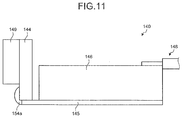
- FIG. 11 is a schematic view illustrating a conventional imaging unit.
- the imaging unit is viewed in a direction orthogonal to an optical axis direction and orthogonal to a stacking direction of a multi-layer substrate.
- a conventional imaging unit 140 has a configuration in which a substrate 145 extends in the optical axis direction from an imaging element 144.
- the imaging element 144 has a light-receiving surface covered with a glass lid 149.
- the substrate 145 is electrically connected to the imaging element 144 by an inner lead, which is not illustrated, and a connected part thereof is sealed with an adhesive 154a.
- a multi-layer substrate 146 is formed on the substrate 145, and a distal end of a signal cable 148 is connected to a proximal end portion of the multi-layer substrate 146.
- Patent Literature 1 JP 2005-304876 A
- an endoscope apparatus accompanied with forward and backward operation of an insertion unit as well as a bending movement thereof for adjusting a camera angle during use of an endoscope, a force pushing in a distal end direction or a force shaking up and down and twisting is applied to the signal cable 148.
- This causes an upward or downward stress on the substrate 145 and the multi-layer substrate 146 to which the signal cable 148 is connected.
- a central part Sp of the substrate 145 and the multi-layer substrate 146 may be bent.
- a central part of the substrate may be warped by heat and a load during manufacturing of the imaging unit.
- a compact imaging unit has been promoted to reduce a diameter of the insertion unit; however, as the imaging unit becomes smaller, an influence of this bending stress becomes non-negligible, whereby performance of the imaging unit may be degraded.
- the present invention has been made in view of the foregoing, and an object of the invention is to provide an imaging unit and an endoscope apparatus that can achieve a compact distal end of the insertion unit and reduce an influence of a stress unique to the endoscope apparatus.
- an imaging unit includes: a solid state image sensor configured to receive light and perform photoelectric conversion on the light to generate an electric signal; a substrate extending from the solid state image sensor in an optical axis direction of the solid state image sensor; and a multi-layer substrate formed on a surface of the substrate, the multi-layer substrate having a plurality of electronic components mounted thereon and having a plurality of conductor layers and a plurality of via holes formed therein. At least one of the plurality of electronic components is embedded inside the multi-layer substrate. The plurality of via holes is formed on an outer side of the at least one of the plurality of electronic components embedded inside the multi-layer substrate along an optical axis direction of the multi-layer substrate.
- the multi-layer substrate has two or more electronic components among the plurality of electronic components embedded therein.
- the two or more electronic components are adjacently embedded inside the multi-layer substrate such that the via holes are not interposed between the two or more electronic components.
- the at least one of the plurality of electronic components is embedded in a central part of the multi-layer substrate.
- the at least one of the plurality of electronic components embedded inside the multi-layer substrate has a rectangular shape in a plan view in a stacking direction, and is disposed such that a long side of the rectangular shape is orthogonal to the optical axis direction of the multi-layer substrate.
- an interval between the adjacent electronic components is smaller than a minimum value of an interval between the via holes formed inside the multi-layer substrate and the two or more electronic components embedded inside the multi-layer substrate.
- An endoscope apparatus includes an insertion unit having an imaging unit at a distal end of the insertion unit.
- the imaging unit includes: a solid state image sensor configured to receive light and perform photoelectric conversion on the light to generate an electric signal; a substrate extending from the solid state image sensor in an optical axis direction of the solid state image sensor; and a multi-layer substrate formed on a surface of the substrate, the multi-layer substrate having a plurality of electronic components mounted thereon and having a plurality of conductor layers and a plurality of via holes formed therein. At least one of the plurality of electronic components is embedded inside the multi-layer substrate.
- the via holes are formed on an outer side of the at least one of the plurality of electronic components embedded inside the multi-layer substrate along an optical axis direction of the multi-layer substrate.
- At least one of electronic components is embedded in a multi-layer substrate to achieve a compact distal end of the insertion unit.
- a via hole which is susceptible to the stress unique to the endoscope apparatus, is formed in a position which is outside of the electronic components along an optical axis direction of the multi-layer substrate so as to be less susceptible to a bend and a warp.
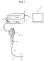
- FIG. 1 is a schematic view illustrating an overall configuration of an endoscope system according to an embodiment of the present invention.
- an endoscope apparatus 1 includes an endoscope 2, a universal code 6, a connector 7, a light source device 9, a processor (control device) 10, and a display device 13.
- the connector 7 is provided to a proximal end of the universal code 6 and is connected to the light source device 9 and the processor 10. It performs predetermined signal processing on the imaging signal, which has been output by the imaging device of the distal end portion 31 connected to the universal code 6, and it performs analog-digital conversion (A/D conversion) on the imaging signal and outputs it as an image signal.
- A/D conversion analog-digital conversion
- the light source device 9 is constituted of a white LED, for example. Pulsed white light lit by the light source device 9 passes through the connector 7 and the universal code 6, and it becomes illumination light to be emitted toward an object from the distal end of the insertion unit 4 of the endoscope 2.
- the processor 10 performs predetermined image processing on the image signal that has been output from the connector 7 and controls the entire endoscope apparatus 1.
- the display device 13 displays the image signal that has been processed by the processor 10.
- An operating unit 5 provided with a variety of buttons and knobs for operating an endoscope function is connected to a proximal end side of the insertion unit 4 of the endoscope 2.
- the operating unit 5 is provided with a treatment tool insertion opening 17 through which a treatment tool, such as a biological forceps, an electric knife, and an inspection probe, is inserted into the body cavity of the subject.
- the insertion unit 4 is constituted of the distal end portion 31 provided with the imaging device, a bending portion 32 freely bendable in multiple directions and connected to a proximal end side of the distal end portion 31, and a flexible tube portion 33 connected to a proximal end side of the bending portion 32.
- the bending portion 32 is bent by operating a knob for bending operation provided to the operating unit 5. It is freely bendable in four directions of up, down, right, and left, for example, by pulling and relaxing a bending wire, which is inserted inside the insertion unit 4.
- a light guide bundle (not illustrated) that transmits the illumination light from the light source device 9 is arranged to the endoscope 2.
- An illumination lens (not illustrated) is disposed at an emitting end of the illumination light from the light guide bundle. This illumination lens is provided to the distal end portion 31 of the insertion unit 4, and the illumination light is emitted toward the subject.
- FIG. 2 is a sectional view of a part of a distal end of the endoscope 2.
- FIG. 2 is a sectional view cut through a surface orthogonal to a substrate surface of the imaging unit, or a surface parallel to an optical axis direction of the imaging unit.
- the imaging unit is provided to the distal end portion 31 of the endoscope 2.
- the distal end portion 31 and a part of the bending portion 32 of the insertion unit 4 of the endoscope 2 are illustrated.
- the bending portion 32 is freely bendable in four directions of up, down, right, and left by pulling and relaxing a bending wire 82 inserted inside a bending tube 81 disposed inside a covering tube 42 to be described below.
- An imaging device 35 is provided inside the distal end portion 31, which extends on a distal end side of the bending portion 32.
- the distal end portion 31 in which the distal end portion main body 41 is disposed is a hard part of the insertion unit 4.
- a length La of this hard part ranges from the distal end of the insertion unit 4 to the proximal end of the distal end portion main body 41.
- a length Lb corresponds to an outside diameter of the distal end of the insertion unit 4.
- the lens unit 43 has a plurality of objective lenses 43a-1 to 43a-4 and a lens holder 43b that holds the objective lenses 43a-1 to 43a-4.
- a distal end of the lens holder 43b is inserted inside and fixed to the distal end portion main body 41, whereby the lens unit 43 is fixed to the distal end portion main body 41.
- the imaging unit 40 includes a solid state image sensor 44 that generates an electric signal by receiving light of a CCD or a CMOS and performing photoelectric conversion thereon, a substrate 45 extending from the solid state image sensor 44 in an optical axis direction, a multi-layer substrate 46 having multiple conductor layers on a surface of the substrate 45, and a glass lid 49 adhered to the solid state image sensor 44 in a state of covering a light-receiving surface of the solid state image sensor 44.
- electronic components 55 to 58 constituting a driving circuit of the solid state image sensor 44 are mounted, and via holes 71 and 73 that electrically conduct between the plurality of conductor layers are formed therein.
- a distal end of each of signal cables 48 of an electric cable bundle 47 is connected. Note that on the multi-layer substrate 46, an electronic component other than the ones constituting the driving circuit of the solid state image sensor 44 may also be mounted.
- a proximal end of each of the signal cables 48 extends in a direction of a proximal end of the insertion unit 4.
- the electric cable bundle 47 is inserted and disposed in the insertion unit 4, and it extends to the connector 7 through the operating unit 5 and the universal code 6 illustrated in FIG. 1 .
- a subject image that has been image-formed by the objective lenses 43a-1 to 43a-4 of the lens unit 43 is detected by the solid state image sensor 44, which is arranged in an image-forming position of the objective lenses 43a-1 to 43a-4, and is converted into an imaging signal.
- the imaging signal is output to the processor 10 through the signal cables 48, which are connected to the substrate 45 and the multi-layer substrate 46, and the connector 7.
- the solid state image sensor 44 is adhered to the substrate 45 and the multi-layer substrate 46.
- the solid state image sensor 44 and a connecting part of the solid state image sensor 44 and the substrate 45 are covered with a metal reinforcement member 52.
- the reinforcement member 52 is installed in a separated manner from the solid state image sensor 44, the substrate 45, and the multi-layer substrate 46.
- a distal end portion of the imaging unit 40 and the electric cable bundle 47 is covered with a heat shrinkable tube 50 on an outer periphery thereof. Inside the heat shrinkable tube 50, space between components is filled with an adhesive resin 51.
- a solid state image sensor holder 53 holds the solid state image sensor 44, which is adhered to the glass lid 49, by fitting an outer periphery surface of the glass lid 49 into an inner periphery surface on the proximal end side of the solid state image sensor holder 53.
- the outer periphery surface on the proximal end side of the solid state image sensor holder 53 is fitted into an inner periphery surface on a distal end side of the reinforcement member 52.
- An outer periphery surface on the proximal end side of the lens holder 43b is fitted into the inner periphery surface on the distal end side of the solid state image sensor holder 53.
- the outer periphery surface of the lens holder 43b, the outer periphery surface of the solid state image sensor holder 53, and an outer periphery surface on a distal end side of the heat shrinkable tube 50 are fixed to an inner periphery surface on a distal end of the distal end portion main body 41 with the adhesive 41a.
- FIG. 3 is a plan view of the imaging unit 40 planarly viewed in a stacking direction.
- FIG. 4 is a sectional view of line A-A in FIG. 3 , or a sectional view when the imaging unit 40 is cut through a surface vertical to a surface of the substrate 45 and parallel to an optical axis direction of the solid state image sensor 44.
- FIGS. 3 and 4 for a description purpose, there is illustrated a plane Ls that passes through a center of the multi-layer substrate 46 and bisects a length in an optical axis direction of the multi-layer substrate 46.
- an inner lead (not illustrated) of the substrate 45 is electrically connected to a lower electrode (not illustrated) of the solid state image sensor 44, which are covered with a sealing resin 54a, whereby the solid state image sensor 44 and the substrate 45 are connected to each other.
- the substrate 45 is a flexible printed substrate, and it extends from the solid state image sensor 44 in the optical axis direction of the solid state image sensor 44.
- the multi-layer substrate 46 is formed in which multiple layers are stacked, and the multi-layer substrate 46 is electrically and mechanically connected to the substrate 45.
- a back surface of the solid state image sensor 44 is adhered to a side surface of the multi-layer substrate 46 on a side of the solid state image sensor 44 with an adhesive 54b.
- the imaging unit 40 is disposed such that the whole imaging unit 40 including the substrate 45, the multi-layer substrate 46, the electronic components 55 to 58, and the signal cables 48 fits within a projection region, which is obtained by projecting the solid state image sensor 44 in the optical axis direction.
- connection lands 61 On the multi-layer substrate 46, there are formed two connection lands 61 to which the electronic component 55 is electrically connected, two connection lands 62 to which the electronic component 56 is connected, and a cable connection land 63 to which a conductor at a distal end of the signal cable 48 is electrically and mechanically connected.
- six cable connection lands 63 are provided, whereby six signal cables 48 can be connected thereto by solder and the like.
- connection lands 64, 65A, 65B, and 66 electrically connected to the substrate 45.
- a plurality of conductor layers is layered. In a section illustrated in FIG. 4 , conductor layers 67, 68, and 69 are illustrated. Inside the multi-layer substrate 46, a plurality of via holes 71 to 76 is formed. The plurality of conductor layers including the conductor layers 67 to 69 is formed so as to be electrically connected to any of the plurality of via holes 71 to 76.
- connection land 61 on the upper surface of the multi-layer substrate 46, to which the electronic component 55 is electrically connected is electrically connected to the two connection lands 64 (only one is illustrated in FIG. 4 ) on a lower surface side of the multi-layer substrate 46 through the via holes 71 and 72 and the conductor layer 67.
- the connection land 62 on the upper surface of the multi-layer substrate 46, to which the electronic component 56 is electrically connected is electrically connected to the two connection lands 65A (only one is illustrated in FIG. 4 ) on the lower surface side of the multi-layer substrate 46 through a via hole that is not illustrated.
- the electronic component 57 which is embedded in the multi-layer substrate 46, is electrically connected to the conductor layer 67, whereby it is electrically connected to the electronic component 55 and the connection land 64 through the via hole 71.
- the electronic component 58 is electrically connected to the conductor layer 68, whereby it is electrically connected to the two connection lands 65B (only one is illustrated in FIG. 4 ) on the lower surface side of the multi-layer substrate 46 through a via hole that is not illustrated.
- a cable connection land that is the second from the bottom relative to a shorter side direction of the substrate 45 is electrically connected to the connection land 66 on the lower surface side of the multi-layer substrate 46 through the via hole 76, the conductor layer 69, and the via hole 73.
- the electronic components 57 and 58 are embedded inside the multi-layer substrate 46 so as to avoid the plane Ls, which passes through a center in the optical axis direction of the multi-layer substrate 46.
- all of the via holes 71 to 76 are formed on an outer side of the multi-layer substrate 46 in the optical axis direction of the multi-layer substrate 46 relative to the electronic components 57 and 58, which are embedded inside the multi-layer substrate 46.
- the electronic component 57 and the electronic component 58, which are embedded inside the multi-layer substrate 46 are embedded inside the multi-layer substrate 46 so as to be adjacent to each other without interposing any via hole.
- these two or more electronic components are embedded inside the multi-layer substrate so as to be adjacent to each other without interposing any via hole.
- the electronic components 57 and 58 are embedded in a part near the center in the optical axis direction of the multi-layer substrate 46, and the via holes 71 to 76 are formed in a part at an end in the optical axis direction of the multi-layer substrate 46 outside the electronic components 57 and 58. Note that in the imaging unit 40 illustrated in FIGS.
- a long side direction of the substrate 45 and the multi-layer substrate 46 corresponds to the optical axis direction whereas a shorter side direction of the substrate 45 and the multi-layer substrate 46 corresponds to a direction orthogonal to both of the optical axis direction and the stacking direction.
- a force pushing in a distal end direction or a force shaking up and down and twisting is applied to the signal cable 48.
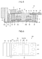
- a stress is caused to the multi-layer substrate 46 and the substrate 45, to which the signal cables 48 are connected, due to this, as illustrated in FIG. 5 , a central part Sc of the substrate 45 and the multi-layer substrate 46 may be bent.
- an electronic component is formed of a hard material such as ceramic, whereby the electronic component itself is relatively less deformable by the bending stress unique to the endoscope.
- a via hole is more susceptible to the bending stress than the electronic component.
- a land or a conductor layer to which the via hole is connected may also be deformed, whereby it may be peeled off from the via hole.
- conduction of the via hole becomes unstable, whereby it may cause degradation of performance of the imaging unit such as occurrence of noise in an image.
- component arrangement is set such that the electronic components 57 and 58 are embedded in a part near the center in the optical axis direction of the multi-layer substrate 46, and the via holes 71 to 76 are formed in the part at an end in the optical axis direction of the multi-layer substrate 46 outside the electronic components 57 and 58. Then, in the imaging unit 40, at the center of the multi-layer substrate 46, none of the via holes 71 to 76 and the electronic components 57 and 58 is disposed. Thus, as in FIG. 5 , since the electronic components 57 and 58 and the via holes 71, 73, and 76 are not located at the central part Sc of the multi-layer substrate 46 where a bend is caused by the stress, these are not affected by the stress.
- the via holes 71 to 76 are disposed near the end in the optical axis direction of the multi-layer substrate 46 where the stress is less likely to be applied and is less deformable than the central part, whereby an influence of the stress on the via holes 71 to 76 is suppressed as much as possible.
- the imaging unit 40 it is possible to reduce instability of the conduction of the via holes 71 to 76 and to achieve high reliability.
- the electronic components 57 and 58 are embedded inside the multi-layer substrate 46 on an inner side relative to the via holes 71 to 76.
- the imaging unit 40 it is possible to install the electronic components 57 and 58 in a position where the two electronic components 55 and 56 mounted on the upper surface of the multi-layer substrate 46 are superimposed on the connection lands 61 and 62 of the electronic components 55 and 56 in a top view.
- the imaging unit 40 it is possible to reduce an area of the substrate in the top view compared to a configuration having a component arrangement of disposing all of four electronic components in addition to the cable connection land on the upper surface of the multi-layer substrate, whereby it is possible to achieve a compact imaging unit.
- three via holes 73 to 75 are disposed at an end of the substrate 45 on the same straight line parallel to the shorter side direction of the multi-layer substrate 46; however, the component arrangement is not limited to this.
- three via holes 271 to 273 on a solid state image sensor 44 side may be disposed zigzag along a direction orthogonal to an optical axis.
- three via holes 274 to 276 on a proximal end side may also be disposed zigzag along the direction orthogonal to the optical axis.
- a width in the shorter side direction of the substrate and the multi-layer substrate can be reduced while securing an interval between the via holes.
- a zigzag arrangement close to a straight line is used by reducing the interval between the adjacent via holes.
- illustration of the electronic components and the connection lands mounted on the upper surface of the multi-layer substrate 46 is omitted for a description purpose.
- the electronic components 57 and 58 are embedded in the central part of the multi-layer substrate 46 along the optical axis direction without interposing the via holes 271 to 276 therebetween. Since it is possible to mount the electronic components at high density by a surface mount technology, among two or more electronic components embedded in the multi-layer substrate 46 of the plurality of electronic components 55 to 58, the interval between two or more adjacent electronic components may be an interval De that is smaller than a minimum value Db of the interval between the via hole formed inside the multi-layer substrate 46 and the electronic components embedded inside the multi-layer substrate 46.
- the electronic component is formed of the hard material as described above, it is relatively less deformable by the bending stress unique to the endoscope. Accordingly, the influence of the stress on the electronic component is small, whereby it is possible to embed the two electronic components 57 and 58 in a proximate state inside the multi-layer substrate 46 at the central part thereof.
- the component arrangement in which the two electronic components 57 and 58 are embedded in the proximate state without interposing a via hole inside the multi-layer substrate near the center thereof as well as the via holes 271 to 276 are formed at the end in the optical axis direction of the multi-layer substrate 46 may be the most preferred component arrangement of this embodiment because the length in the optical axis direction of the multi-layer substrate 46 can be reduced the most while securing the interval between each of the members.
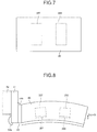
- FIG. 7 is a schematic view illustrating a method of arranging the electronic component used in the embodiment, and it is a plan view of the imaging unit planarly viewed in the stacking direction.
- FIG. 7 for a description purpose, illustration of a member other than the multi-layer substrate and the electronic component is omitted.
- FIG. 8 is a schematic view illustrating how the imaging unit illustrated in FIG. 7 is deformed by receiving the stress. In FIG. 8 , the deformed imaging unit is viewed in the direction orthogonal to both of the optical axis direction and the stacking direction.
- FIG. 7 is a schematic view illustrating a method of arranging the electronic component used in the embodiment, and it is a plan view of the imaging unit planarly viewed in the stacking direction.
- illustration of a member other than the multi-layer substrate and the electronic component is omitted.
- FIG. 8 is a schematic view illustrating how the imaging unit illustrated in FIG. 7 is deformed by receiving the stress. In FIG. 8 , the deformed imaging unit is
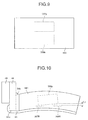
- FIG. 9 is a plan view illustrating a method of arranging the electronic component not used in the embodiment, and it is a plan view planarly viewed in the stacking direction.
- FIG. 10 is a schematic view illustrating how the imaging unit illustrated in FIG. 9 is deformed by receiving the stress. In FIG. 10 , the deformed imaging unit is viewed in the direction orthogonal to both of the optical axis direction and the stacking direction.
- the electronic components 357 and 358 embedded inside the multi-layer substrate 46 are rectangular when planarly viewed in the stacking direction, the electronic components 357 and 358 are disposed such that a long side of a rectangle is in a direction orthogonal to the optical axis direction of the multi-layer substrate 46.
- the multi-layer substrate 46 is deformed according to the stress as illustrated in FIG. 8 .
- the electronic components 357 and 358 are less deformable; however, since a length in the optical axis direction of the electronic components 357 and 358 is small relative to that of the multi-layer substrate 46, even in a case where the electronic components 357 and 358 are not capable of following the deformation of the multi-layer substrate 46, a width Cr (see FIG. 8 ) of lifting of the electronic components 357 and 358 from conductor layers 367 and 368 is very small, whereby performance of the imaging unit is hardly degraded.
- a length in the optical axis direction of the electronic components 357p and 358p is long relative to that of the multi-layer substrate 46C. Since the electronic components 357p and 358p are less deformable, when the multi-layer substrate 46C is deformed, the electronic component 358p is not capable of following the deformation of the multi-layer substrate 46C, whereby it may peel off from conductor layers 368R and 368L (see FIG. 10 ), which are deformed following the deformation of the multi-layer substrate 46C.
- the electronic component 368p peels off from an upper surface of the conductor layer 368R, and a lower surface of the electronic component 358p is lifted from the upper surface of the conductor layer 368R by a width Cp, which is large compared to the width Cr.
- a width Cp which is large compared to the width Cr.
- a planar shape of the electronic component embedded inside the multi-layer substrate is a rectangle when planarly viewed in the stacking direction
- by disposing the electronic component such that the long side of the rectangle is in an direction orthogonal to the optical axis direction of the multi-layer substrate it is possible to reduce the influence of the stress on the electronic component is reduced, whereby stabilization of the performance of the imaging unit is achieved.
Landscapes
- Physics & Mathematics (AREA)
- Engineering & Computer Science (AREA)
- Optics & Photonics (AREA)
- Health & Medical Sciences (AREA)
- Life Sciences & Earth Sciences (AREA)
- Multimedia (AREA)
- Astronomy & Astrophysics (AREA)
- General Physics & Mathematics (AREA)
- Microelectronics & Electronic Packaging (AREA)
- Surgery (AREA)
- Signal Processing (AREA)
- Pathology (AREA)
- Molecular Biology (AREA)
- Radiology & Medical Imaging (AREA)
- Biophysics (AREA)
- Biomedical Technology (AREA)
- Heart & Thoracic Surgery (AREA)
- Medical Informatics (AREA)
- Nuclear Medicine, Radiotherapy & Molecular Imaging (AREA)
- Animal Behavior & Ethology (AREA)
- General Health & Medical Sciences (AREA)
- Public Health (AREA)
- Veterinary Medicine (AREA)
- Endoscopes (AREA)
- Instruments For Viewing The Inside Of Hollow Bodies (AREA)
- Studio Devices (AREA)
Abstract
Description
- The present invention relates to an imaging unit provided at a distal end of an insertion unit of an endoscope that is configured to be inserted into a subject for capturing an image of an inside the subject, and relates to an endoscope apparatus.
- In medical and industrial fields, endoscope apparatuses have conventionally been used widely in a variety of examinations. Among these endoscope apparatuses, a medical endoscope apparatus has been used widely since it is capable of obtaining an in-vivo image inside a body cavity without incising the subject by inserting a flexible insertion unit, which has an elongated shape and is provided with an imaging element at a distal end thereof, inside the body cavity of the subject such as a patient, and furthermore, it is capable of performing a therapeutic treatment as necessary by protruding a treatment tool from the distal end of the insertion unit.
- An imaging unit including an imaging element and a lens unit that performs image-formation of a subject image on a light-receiving surface of the imaging element (for example, see Patent Literature 1) are fitted to the distal end of the insertion unit of such endoscope apparatus.
-
FIG. 11 is a schematic view illustrating a conventional imaging unit. InFIG. 11 , the imaging unit is viewed in a direction orthogonal to an optical axis direction and orthogonal to a stacking direction of a multi-layer substrate. As illustrated inFIG. 11 , aconventional imaging unit 140 has a configuration in which asubstrate 145 extends in the optical axis direction from animaging element 144. Theimaging element 144 has a light-receiving surface covered with aglass lid 149. Thesubstrate 145 is electrically connected to theimaging element 144 by an inner lead, which is not illustrated, and a connected part thereof is sealed with an adhesive 154a. Amulti-layer substrate 146 is formed on thesubstrate 145, and a distal end of asignal cable 148 is connected to a proximal end portion of themulti-layer substrate 146. - Patent Literature 1:
JP 2005-304876 A - In an endoscope apparatus, accompanied with forward and backward operation of an insertion unit as well as a bending movement thereof for adjusting a camera angle during use of an endoscope, a force pushing in a distal end direction or a force shaking up and down and twisting is applied to the
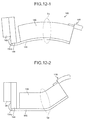
signal cable 148. This causes an upward or downward stress on thesubstrate 145 and themulti-layer substrate 146 to which thesignal cable 148 is connected. Accordingly, as illustrated inFIGS. 12-1 and 12-2 , a central part Sp of thesubstrate 145 and themulti-layer substrate 146 may be bent. In an imaging unit of the endoscope, a central part of the substrate may be warped by heat and a load during manufacturing of the imaging unit. In the endoscope apparatus, a compact imaging unit has been promoted to reduce a diameter of the insertion unit; however, as the imaging unit becomes smaller, an influence of this bending stress becomes non-negligible, whereby performance of the imaging unit may be degraded. - The present invention has been made in view of the foregoing, and an object of the invention is to provide an imaging unit and an endoscope apparatus that can achieve a compact distal end of the insertion unit and reduce an influence of a stress unique to the endoscope apparatus. Solution to Problem
- To solve the problem described above and to achieve the object, an imaging unit according to the invention includes: a solid state image sensor configured to receive light and perform photoelectric conversion on the light to generate an electric signal; a substrate extending from the solid state image sensor in an optical axis direction of the solid state image sensor; and a multi-layer substrate formed on a surface of the substrate, the multi-layer substrate having a plurality of electronic components mounted thereon and having a plurality of conductor layers and a plurality of via holes formed therein. At least one of the plurality of electronic components is embedded inside the multi-layer substrate. The plurality of via holes is formed on an outer side of the at least one of the plurality of electronic components embedded inside the multi-layer substrate along an optical axis direction of the multi-layer substrate.
- In the imaging unit according to the invention, the multi-layer substrate has two or more electronic components among the plurality of electronic components embedded therein. The two or more electronic components are adjacently embedded inside the multi-layer substrate such that the via holes are not interposed between the two or more electronic components.
- In the imaging unit according to the invention, the at least one of the plurality of electronic components is embedded in a central part of the multi-layer substrate.
- In the imaging unit according to the invention, the at least one of the plurality of electronic components embedded inside the multi-layer substrate has a rectangular shape in a plan view in a stacking direction, and is disposed such that a long side of the rectangular shape is orthogonal to the optical axis direction of the multi-layer substrate.
- In the imaging unit according to the invention, among the two or more electronic components embedded inside the multi-layer substrate, an interval between the adjacent electronic components is smaller than a minimum value of an interval between the via holes formed inside the multi-layer substrate and the two or more electronic components embedded inside the multi-layer substrate.
- In the imaging unit according to the invention, a back surface of the solid state image sensor is adhered to a side surface of the multi-layer substrate.
- An endoscope apparatus according to the invention includes an insertion unit having an imaging unit at a distal end of the insertion unit. The imaging unit includes: a solid state image sensor configured to receive light and perform photoelectric conversion on the light to generate an electric signal; a substrate extending from the solid state image sensor in an optical axis direction of the solid state image sensor; and a multi-layer substrate formed on a surface of the substrate, the multi-layer substrate having a plurality of electronic components mounted thereon and having a plurality of conductor layers and a plurality of via holes formed therein. At least one of the plurality of electronic components is embedded inside the multi-layer substrate. The via holes are formed on an outer side of the at least one of the plurality of electronic components embedded inside the multi-layer substrate along an optical axis direction of the multi-layer substrate.
- According to the present invention, at least one of electronic components is embedded in a multi-layer substrate to achieve a compact distal end of the insertion unit. In addition, a via hole, which is susceptible to the stress unique to the endoscope apparatus, is formed in a position which is outside of the electronic components along an optical axis direction of the multi-layer substrate so as to be less susceptible to a bend and a warp. With this component arrangement, it is possible to reduce an influence of the stress unique to the endoscope apparatus.
-
-
FIG. 1 is a schematic view illustrating an overall configuration of an endoscope system according to an embodiment of the present invention. -
FIG. 2 is a sectional view of a part of a distal end of an endoscope illustrated inFIG. 1 . -
FIG. 3 is a plan view of an imaging unit illustrated inFIG. 2 planarly viewed in a stacking direction. -
FIG. 4 is a sectional view of line A-A inFIG. 3 . -
FIG. 5 is a schematic view illustrating a force applied to the imaging unit illustrated inFIG. 3 and is a sectional view of the imaging unit. -
FIG. 6 is a plan view of another example of the imaging unit illustrated inFIG. 2 planarly viewed in the stacking direction. -
FIG. 7 is a plan view illustrating a method of arranging an electronic component used in the embodiment. -
FIG. 8 is a schematic view illustrating how the imaging unit illustrated inFIG. 7 is deformed by receiving a stress. -
FIG. 9 is a plan view illustrating a method of arranging the electronic component not used in the embodiment. -
FIG. 10 is a schematic view illustrating how the imaging unit illustrated inFIG. 9 is deformed by receiving a stress. -
FIG. 11 is a schematic view illustrating a conventional imaging unit. -
FIG. 12-1 is a schematic view illustrating a force applied to the imaging unit. -
FIG. 12-2 is a schematic view illustrating the force applied to the imaging unit. - Reference will be made below to an endoscope apparatus provided with an imaging unit as modes for carrying out the present invention (hereinafter, referred to as "embodiment(s)"). The present invention is not to be limited by the embodiment(s). The same reference signs are used to refer to the same elements throughout the drawings. The drawings are schematic, and it is to be noted that a relationship between thickness and width of each member, a ratio between each of the members, and the like may be different from actualities. Also, there may be a part having a difference in size or ratio between the drawings.
-
FIG. 1 is a schematic view illustrating an overall configuration of an endoscope system according to an embodiment of the present invention. As illustrated inFIG. 1 , anendoscope apparatus 1 includes anendoscope 2, auniversal code 6, a connector 7, alight source device 9, a processor (control device) 10, and adisplay device 13. - By inserting an
insertion unit 4 inside a body cavity of a subject, theendoscope 2 captures an in-vivo image of the subject and outputs an imaging signal. An electric cable bundle inside theuniversal code 6 is extended to a distal end of theinsertion unit 4 of theendoscope 2 and is connected to an imaging device, which is provided to adistal end portion 31 of theinsertion unit 4. - The connector 7 is provided to a proximal end of the
universal code 6 and is connected to thelight source device 9 and theprocessor 10. It performs predetermined signal processing on the imaging signal, which has been output by the imaging device of thedistal end portion 31 connected to theuniversal code 6, and it performs analog-digital conversion (A/D conversion) on the imaging signal and outputs it as an image signal. - The
light source device 9 is constituted of a white LED, for example. Pulsed white light lit by thelight source device 9 passes through the connector 7 and theuniversal code 6, and it becomes illumination light to be emitted toward an object from the distal end of theinsertion unit 4 of theendoscope 2. - The
processor 10 performs predetermined image processing on the image signal that has been output from the connector 7 and controls theentire endoscope apparatus 1. Thedisplay device 13 displays the image signal that has been processed by theprocessor 10. - An
operating unit 5 provided with a variety of buttons and knobs for operating an endoscope function is connected to a proximal end side of theinsertion unit 4 of theendoscope 2. Theoperating unit 5 is provided with a treatmenttool insertion opening 17 through which a treatment tool, such as a biological forceps, an electric knife, and an inspection probe, is inserted into the body cavity of the subject. - The
insertion unit 4 is constituted of thedistal end portion 31 provided with the imaging device, a bendingportion 32 freely bendable in multiple directions and connected to a proximal end side of thedistal end portion 31, and aflexible tube portion 33 connected to a proximal end side of the bendingportion 32. The bendingportion 32 is bent by operating a knob for bending operation provided to theoperating unit 5. It is freely bendable in four directions of up, down, right, and left, for example, by pulling and relaxing a bending wire, which is inserted inside theinsertion unit 4. - A light guide bundle (not illustrated) that transmits the illumination light from the
light source device 9 is arranged to theendoscope 2. An illumination lens (not illustrated) is disposed at an emitting end of the illumination light from the light guide bundle. This illumination lens is provided to thedistal end portion 31 of theinsertion unit 4, and the illumination light is emitted toward the subject. - Next, reference will be made in detail to a configuration of the
distal end portion 31 of theendoscope 2.FIG. 2 is a sectional view of a part of a distal end of theendoscope 2.FIG. 2 is a sectional view cut through a surface orthogonal to a substrate surface of the imaging unit, or a surface parallel to an optical axis direction of the imaging unit. The imaging unit is provided to thedistal end portion 31 of theendoscope 2. InFIG. 2 , thedistal end portion 31 and a part of the bendingportion 32 of theinsertion unit 4 of theendoscope 2 are illustrated. - As illustrated in
FIG. 2 , the bendingportion 32 is freely bendable in four directions of up, down, right, and left by pulling and relaxing abending wire 82 inserted inside a bendingtube 81 disposed inside a coveringtube 42 to be described below. Animaging device 35 is provided inside thedistal end portion 31, which extends on a distal end side of the bendingportion 32. - The
imaging device 35 has alens unit 43 and animaging unit 40 disposed on a proximal end side of thelens unit 43, which are adhered to inside of a distal end portionmain body 41 with an adhesive 41a. The distal end portionmain body 41 is constituted of a hard member to form an internal space in which theimaging device 35 is housed. An outer periphery portion of a proximal end of the distal end portionmain body 41 is covered with thepliable covering tube 42. Such that the bendingportion 32 can be bent, any member that is located on a proximal end side of the distal end portionmain body 41 is constituted of a pliable member. Thedistal end portion 31 in which the distal end portionmain body 41 is disposed is a hard part of theinsertion unit 4. A length La of this hard part ranges from the distal end of theinsertion unit 4 to the proximal end of the distal end portionmain body 41. Note that a length Lb corresponds to an outside diameter of the distal end of theinsertion unit 4. - The
lens unit 43 has a plurality ofobjective lenses 43a-1 to 43a-4 and alens holder 43b that holds theobjective lenses 43a-1 to 43a-4. A distal end of thelens holder 43b is inserted inside and fixed to the distal end portionmain body 41, whereby thelens unit 43 is fixed to the distal end portionmain body 41. - The
imaging unit 40 includes a solidstate image sensor 44 that generates an electric signal by receiving light of a CCD or a CMOS and performing photoelectric conversion thereon, asubstrate 45 extending from the solidstate image sensor 44 in an optical axis direction, amulti-layer substrate 46 having multiple conductor layers on a surface of thesubstrate 45, and aglass lid 49 adhered to the solidstate image sensor 44 in a state of covering a light-receiving surface of the solidstate image sensor 44. To themulti-layer substrate 46 of theimaging unit 40,electronic components 55 to 58 constituting a driving circuit of the solidstate image sensor 44 are mounted, and viaholes multi-layer substrate 46, a distal end of each ofsignal cables 48 of anelectric cable bundle 47 is connected. Note that on themulti-layer substrate 46, an electronic component other than the ones constituting the driving circuit of the solidstate image sensor 44 may also be mounted. - A proximal end of each of the
signal cables 48 extends in a direction of a proximal end of theinsertion unit 4. Theelectric cable bundle 47 is inserted and disposed in theinsertion unit 4, and it extends to the connector 7 through theoperating unit 5 and theuniversal code 6 illustrated inFIG. 1 . - A subject image that has been image-formed by the
objective lenses 43a-1 to 43a-4 of thelens unit 43 is detected by the solidstate image sensor 44, which is arranged in an image-forming position of theobjective lenses 43a-1 to 43a-4, and is converted into an imaging signal. The imaging signal is output to theprocessor 10 through thesignal cables 48, which are connected to thesubstrate 45 and themulti-layer substrate 46, and the connector 7. - The solid
state image sensor 44 is adhered to thesubstrate 45 and themulti-layer substrate 46. The solidstate image sensor 44 and a connecting part of the solidstate image sensor 44 and thesubstrate 45 are covered with ametal reinforcement member 52. To prevent an influence of external static electricity on theelectronic components 55 to 58 on thesubstrate 45, thereinforcement member 52 is installed in a separated manner from the solidstate image sensor 44, thesubstrate 45, and themulti-layer substrate 46. - To improve tolerance, a distal end portion of the
imaging unit 40 and theelectric cable bundle 47 is covered with aheat shrinkable tube 50 on an outer periphery thereof. Inside theheat shrinkable tube 50, space between components is filled with anadhesive resin 51. - A solid state
image sensor holder 53 holds the solidstate image sensor 44, which is adhered to theglass lid 49, by fitting an outer periphery surface of theglass lid 49 into an inner periphery surface on the proximal end side of the solid stateimage sensor holder 53. The outer periphery surface on the proximal end side of the solid stateimage sensor holder 53 is fitted into an inner periphery surface on a distal end side of thereinforcement member 52. An outer periphery surface on the proximal end side of thelens holder 43b is fitted into the inner periphery surface on the distal end side of the solid stateimage sensor holder 53. In a state where these members are fitted into each other in this way, the outer periphery surface of thelens holder 43b, the outer periphery surface of the solid stateimage sensor holder 53, and an outer periphery surface on a distal end side of theheat shrinkable tube 50 are fixed to an inner periphery surface on a distal end of the distal end portionmain body 41 with the adhesive 41a. - Next, reference will be made to the
imaging unit 40.FIG. 3 is a plan view of theimaging unit 40 planarly viewed in a stacking direction.FIG. 4 is a sectional view of line A-A inFIG. 3 , or a sectional view when theimaging unit 40 is cut through a surface vertical to a surface of thesubstrate 45 and parallel to an optical axis direction of the solidstate image sensor 44. InFIGS. 3 and 4 , for a description purpose, there is illustrated a plane Ls that passes through a center of themulti-layer substrate 46 and bisects a length in an optical axis direction of themulti-layer substrate 46. - As illustrated in
FIGS. 3 and 4 , in theimaging unit 40, an inner lead (not illustrated) of thesubstrate 45 is electrically connected to a lower electrode (not illustrated) of the solidstate image sensor 44, which are covered with a sealingresin 54a, whereby the solidstate image sensor 44 and thesubstrate 45 are connected to each other. - The
substrate 45 is a flexible printed substrate, and it extends from the solidstate image sensor 44 in the optical axis direction of the solidstate image sensor 44. On the surface of thesubstrate 45, themulti-layer substrate 46 is formed in which multiple layers are stacked, and themulti-layer substrate 46 is electrically and mechanically connected to thesubstrate 45. A back surface of the solidstate image sensor 44 is adhered to a side surface of themulti-layer substrate 46 on a side of the solidstate image sensor 44 with an adhesive 54b. - Among a plurality of electronic components constituting the driving circuit of the solid
state image sensor 44, one or more of the electronic components are mounted on an upper surface of themulti-layer substrate 46, and one or more of the electronic components are also embedded inside themulti-layer substrate 46. In the example inFIGS. 3 and 4 , among the plurality ofelectronic components 55 to 58, twoelectronic components multi-layer substrate 46. Then, among the plurality ofelectronic components 55 to 58, twoelectronic components multi-layer substrate 46. Theimaging unit 40 is disposed such that thewhole imaging unit 40 including thesubstrate 45, themulti-layer substrate 46, theelectronic components 55 to 58, and thesignal cables 48 fits within a projection region, which is obtained by projecting the solidstate image sensor 44 in the optical axis direction. - On the
multi-layer substrate 46, there are formed two connection lands 61 to which theelectronic component 55 is electrically connected, two connection lands 62 to which theelectronic component 56 is connected, and acable connection land 63 to which a conductor at a distal end of thesignal cable 48 is electrically and mechanically connected. In the example inFIG. 3 , six cable connection lands 63 are provided, whereby sixsignal cables 48 can be connected thereto by solder and the like. On a lower surface of themulti-layer substrate 46, there is formed a plurality of connection lands 64, 65A, 65B, and 66 electrically connected to thesubstrate 45. - Inside the
multi-layer substrate 46, a plurality of conductor layers is layered. In a section illustrated inFIG. 4 , conductor layers 67, 68, and 69 are illustrated. Inside themulti-layer substrate 46, a plurality of viaholes 71 to 76 is formed. The plurality of conductor layers including the conductor layers 67 to 69 is formed so as to be electrically connected to any of the plurality of viaholes 71 to 76. - For example, the
connection land 61 on the upper surface of themulti-layer substrate 46, to which theelectronic component 55 is electrically connected, is electrically connected to the two connection lands 64 (only one is illustrated inFIG. 4 ) on a lower surface side of themulti-layer substrate 46 through the via holes 71 and 72 and theconductor layer 67. Theconnection land 62 on the upper surface of themulti-layer substrate 46, to which theelectronic component 56 is electrically connected, is electrically connected to the twoconnection lands 65A (only one is illustrated inFIG. 4 ) on the lower surface side of themulti-layer substrate 46 through a via hole that is not illustrated. Theelectronic component 57, which is embedded in themulti-layer substrate 46, is electrically connected to theconductor layer 67, whereby it is electrically connected to theelectronic component 55 and theconnection land 64 through the viahole 71. Theelectronic component 58 is electrically connected to theconductor layer 68, whereby it is electrically connected to the twoconnection lands 65B (only one is illustrated inFIG. 4 ) on the lower surface side of themulti-layer substrate 46 through a via hole that is not illustrated. Furthermore, among the cable connection lands 63 on the upper surface of themulti-layer substrate 46, a cable connection land that is the second from the bottom relative to a shorter side direction of thesubstrate 45 is electrically connected to theconnection land 66 on the lower surface side of themulti-layer substrate 46 through the viahole 76, theconductor layer 69, and the viahole 73. - Then, as illustrated in
FIGS. 3 and 4 , theelectronic components multi-layer substrate 46 so as to avoid the plane Ls, which passes through a center in the optical axis direction of themulti-layer substrate 46. Then, all of the via holes 71 to 76 are formed on an outer side of themulti-layer substrate 46 in the optical axis direction of themulti-layer substrate 46 relative to theelectronic components multi-layer substrate 46. Theelectronic component 57 and theelectronic component 58, which are embedded inside themulti-layer substrate 46, are embedded inside themulti-layer substrate 46 so as to be adjacent to each other without interposing any via hole. In this embodiment, in a case where two or more electronic components are embedded inside themulti-layer substrate 46, these two or more electronic components are embedded inside the multi-layer substrate so as to be adjacent to each other without interposing any via hole. Theelectronic components multi-layer substrate 46, and the via holes 71 to 76 are formed in a part at an end in the optical axis direction of themulti-layer substrate 46 outside theelectronic components imaging unit 40 illustrated inFIGS. 3 and 4 , a long side direction of thesubstrate 45 and themulti-layer substrate 46 corresponds to the optical axis direction whereas a shorter side direction of thesubstrate 45 and themulti-layer substrate 46 corresponds to a direction orthogonal to both of the optical axis direction and the stacking direction. - Here, in the
endoscope apparatus 1, accompanied with forward and backward operation of an insertion unit as well as a bending movement thereof for adjusting a camera angle during use of an endoscope, a force pushing in a distal end direction or a force shaking up and down and twisting is applied to thesignal cable 48. In a case where a stress is caused to themulti-layer substrate 46 and thesubstrate 45, to which thesignal cables 48 are connected, due to this, as illustrated inFIG. 5 , a central part Sc of thesubstrate 45 and themulti-layer substrate 46 may be bent. - In general, an electronic component is formed of a hard material such as ceramic, whereby the electronic component itself is relatively less deformable by the bending stress unique to the endoscope. In contrast, a via hole is more susceptible to the bending stress than the electronic component. When an excessive stress is applied to the via hole, accompanied by deformation of a multi-layer substrate, a land or a conductor layer to which the via hole is connected may also be deformed, whereby it may be peeled off from the via hole. When such peeling off of the land or the conductor layer from the via hole occurs, conduction of the via hole becomes unstable, whereby it may cause degradation of performance of the imaging unit such as occurrence of noise in an image.
- In the
imaging unit 40, component arrangement is set such that theelectronic components multi-layer substrate 46, and the via holes 71 to 76 are formed in the part at an end in the optical axis direction of themulti-layer substrate 46 outside theelectronic components imaging unit 40, at the center of themulti-layer substrate 46, none of the via holes 71 to 76 and theelectronic components FIG. 5 , since theelectronic components multi-layer substrate 46 where a bend is caused by the stress, these are not affected by the stress. In addition, in theimaging unit 40, the via holes 71 to 76 are disposed near the end in the optical axis direction of themulti-layer substrate 46 where the stress is less likely to be applied and is less deformable than the central part, whereby an influence of the stress on the via holes 71 to 76 is suppressed as much as possible. Thus, in theimaging unit 40, it is possible to reduce instability of the conduction of the via holes 71 to 76 and to achieve high reliability. - In addition, since the back surface of the solid
state image sensor 44 is adhered and fixed to the side surface of themulti-layer substrate 46 on a side of the solidstate image sensor 44 where the electronic component is mounted with the adhesive 54b, strength of this part is enhanced. Thus, even if a twisting force is applied due to the bending movement thereof for adjusting a camera angle and the like, deformation such as a warp and a bend is less likely to be caused to thesubstrate 45 and themulti-layer substrate 46. - Then, in the
imaging unit 40, theelectronic components multi-layer substrate 46 on an inner side relative to the via holes 71 to 76. Thus, in theimaging unit 40, it is possible to install theelectronic components electronic components multi-layer substrate 46 are superimposed on the connection lands 61 and 62 of theelectronic components imaging unit 40, it is possible to reduce an area of the substrate in the top view compared to a configuration having a component arrangement of disposing all of four electronic components in addition to the cable connection land on the upper surface of the multi-layer substrate, whereby it is possible to achieve a compact imaging unit. - In this embodiment, as illustrated in the plan view in
FIG. 3 , three viaholes 73 to 75 are disposed at an end of thesubstrate 45 on the same straight line parallel to the shorter side direction of themulti-layer substrate 46; however, the component arrangement is not limited to this. For example, in a case where three or more via holes are disposed at the end of the substrate, as animaging unit 40A illustrated inFIG. 6 , three viaholes 271 to 273 on a solidstate image sensor 44 side may be disposed zigzag along a direction orthogonal to an optical axis. In the same way, three viaholes 274 to 276 on a proximal end side may also be disposed zigzag along the direction orthogonal to the optical axis. In a case where the via holes are disposed in this way, with a minimum amount of extension of the substrate in the optical axis direction, a width in the shorter side direction of the substrate and the multi-layer substrate can be reduced while securing an interval between the via holes. In the example inFIG. 6 , in order to reduce the amount of extension of themulti-layer substrate 46 in the optical axis direction, a zigzag arrangement close to a straight line is used by reducing the interval between the adjacent via holes. InFIG. 6 , illustration of the electronic components and the connection lands mounted on the upper surface of themulti-layer substrate 46 is omitted for a description purpose. - In a case where two or more electronic components are embedded in the multi-layer substrate, as illustrated in
FIG. 6 , theelectronic components multi-layer substrate 46 along the optical axis direction without interposing the viaholes 271 to 276 therebetween. Since it is possible to mount the electronic components at high density by a surface mount technology, among two or more electronic components embedded in themulti-layer substrate 46 of the plurality ofelectronic components 55 to 58, the interval between two or more adjacent electronic components may be an interval De that is smaller than a minimum value Db of the interval between the via hole formed inside themulti-layer substrate 46 and the electronic components embedded inside themulti-layer substrate 46. In addition, since the electronic component is formed of the hard material as described above, it is relatively less deformable by the bending stress unique to the endoscope. Accordingly, the influence of the stress on the electronic component is small, whereby it is possible to embed the twoelectronic components multi-layer substrate 46 at the central part thereof. Thus, the component arrangement in which the twoelectronic components holes 271 to 276 are formed at the end in the optical axis direction of themulti-layer substrate 46 may be the most preferred component arrangement of this embodiment because the length in the optical axis direction of themulti-layer substrate 46 can be reduced the most while securing the interval between each of the members. - Reference will be made to a direction of the electronic component embedded inside the
multi-layer substrate 46.FIG. 7 is a schematic view illustrating a method of arranging the electronic component used in the embodiment, and it is a plan view of the imaging unit planarly viewed in the stacking direction. InFIG. 7 , for a description purpose, illustration of a member other than the multi-layer substrate and the electronic component is omitted.FIG. 8 is a schematic view illustrating how the imaging unit illustrated inFIG. 7 is deformed by receiving the stress. InFIG. 8 , the deformed imaging unit is viewed in the direction orthogonal to both of the optical axis direction and the stacking direction.FIG. 9 is a plan view illustrating a method of arranging the electronic component not used in the embodiment, and it is a plan view planarly viewed in the stacking direction.FIG. 10 is a schematic view illustrating how the imaging unit illustrated inFIG. 9 is deformed by receiving the stress. InFIG. 10 , the deformed imaging unit is viewed in the direction orthogonal to both of the optical axis direction and the stacking direction. - As illustrated in
FIG. 7 , in the embodiment, in a case where both ofelectronic components multi-layer substrate 46 are rectangular when planarly viewed in the stacking direction, theelectronic components multi-layer substrate 46. When an upward stress is generated on the substrate, themulti-layer substrate 46 is deformed according to the stress as illustrated inFIG. 8 . In contrast, theelectronic components electronic components multi-layer substrate 46, even in a case where theelectronic components multi-layer substrate 46, a width Cr (seeFIG. 8 ) of lifting of theelectronic components conductor layers - On the other hand, as illustrated in
FIG. 9 , in a case whereelectronic components multi-layer substrate 46C, a length in the optical axis direction of theelectronic components multi-layer substrate 46C. Since theelectronic components multi-layer substrate 46C is deformed, theelectronic component 358p is not capable of following the deformation of themulti-layer substrate 46C, whereby it may peel off fromconductor layers 368R and 368L (seeFIG. 10 ), which are deformed following the deformation of themulti-layer substrate 46C. Specifically, as illustrated inFIG. 10 , the electronic component 368p peels off from an upper surface of theconductor layer 368R, and a lower surface of theelectronic component 358p is lifted from the upper surface of theconductor layer 368R by a width Cp, which is large compared to the width Cr. As a result, conduction between theelectronic component 358p and theconductor layer 368R becomes unstable, and the performance of the imaging unit may be degraded. - Thus, in this embodiment, in a case where a planar shape of the electronic component embedded inside the multi-layer substrate is a rectangle when planarly viewed in the stacking direction, by disposing the electronic component such that the long side of the rectangle is in an direction orthogonal to the optical axis direction of the multi-layer substrate, it is possible to reduce the influence of the stress on the electronic component is reduced, whereby stabilization of the performance of the imaging unit is achieved.
-
- 1 endoscope apparatus
- 2 endoscope
- 4 insertion unit
- 5 operating unit
- 6 universal code
- 7 connector
- 9 light source device
- 10 processor
- 13 display device
- 17 treatment tool insertion opening
- 31 distal end portion
- 32 bending portion
- 33 flexible tube portion
- 35 imaging device
- 40, 40A imaging unit
- 41 distal end portion main body
- 41a adhesive
- 42 covering tube
- 43 lens unit
- 43a-1 to 43a-4 objective lens
- 43b lens holder
- 44 solid state image sensor
- 45, 145 substrate
- 46, 46C, 146 multi-layer substrate
- 47 electric cable bundle
- 48 signal cable
- 49 glass lid
- 50 heat shrinkable tube
- 51 adhesive resin
- 52 reinforcement member
- 53 solid state image sensor holder
- 54a sealing resin
- 54b adhesive
- 55 to 58, 357, 357p, 358, 358p electronic component
- 61 to 64, 65A, 65B, 66 connection land
- 63 cable connection land
- 67 to 69, 367, 368, 368R, 368L conductor layer
- 71 to 76 via hole
- 81 bending tube
- 82 bending wire
Claims (7)
- An imaging unit comprising:a solid state image sensor configured to receive light and perform photoelectric conversion on the light to generate an electric signal;a substrate extending from the solid state image sensor in an optical axis direction of the solid state image sensor; anda multi-layer substrate formed on a surface of the substrate, the multi-layer substrate having a plurality of electronic components mounted thereon and having a plurality of conductor layers and a plurality of via holes formed therein, whereinat least one of the plurality of electronic components is embedded inside the multi-layer substrate, andthe plurality of via holes is formed on an outer side of the at least one of the plurality of electronic components embedded inside the multi-layer substrate along an optical axis direction of the multi-layer substrate.
- The imaging unit according to claim 1, wherein
the multi-layer substrate has two or more electronic components among the plurality of electronic components embedded therein, and
the two or more electronic components are adjacently embedded inside the multi-layer substrate such that the plurality of via holes is not interposed between the two or more electronic components. - The imaging unit according to claim 1, wherein
the at least one of the plurality of electronic components is embedded in a central part of the multi-layer substrate. - The imaging unit according to claim 1, wherein
the at least one of the plurality of electronic components embedded inside the multi-layer substrate has a rectangular shape in a plan view in a stacking direction, and is disposed such that a long side of the rectangular shape is orthogonal to the optical axis direction of the multi-layer substrate. - The imaging unit according to claim 2, wherein
among the two or more electronic components embedded inside the multi-layer substrate, an interval between the adjacent electronic components is smaller than a minimum value of an interval between the plurality of via holes formed inside the multi-layer substrate and the two or more electronic components embedded inside the multi-layer substrate. - The imaging unit according to claim 1, wherein
a back surface of the solid state image sensor is adhered to a side surface of the multi-layer substrate. - An endoscope apparatus comprising an insertion unit having an imaging unit at a distal end of the insertion unit, wherein
the imaging unit comprises:a solid state image sensor configured to receive light and perform photoelectric conversion on the light to generate an electric signal;a substrate extending from the solid state image sensor in an optical axis direction of the solid state image sensor; anda multi-layer substrate formed on a surface of the substrate, the multi-layer substrate having a plurality of electronic components mounted thereon and having a plurality of conductor layers and a plurality of via holes formed therein, whereinat least one of the plurality of electronic components is embedded inside the multi-layer substrate, andthe plurality of via holes is formed on an outer side of the at least one of the plurality of electronic components embedded inside the multi-layer substrate along an optical axis direction of the multi-layer substrate.
Applications Claiming Priority (2)
| Application Number | Priority Date | Filing Date | Title |
|---|---|---|---|
| JP2013136561A JP6307227B2 (en) | 2013-06-28 | 2013-06-28 | Imaging unit and endoscope apparatus |
| PCT/JP2014/062572 WO2014208206A1 (en) | 2013-06-28 | 2014-05-12 | Imaging unit and endoscope device |
Publications (2)
| Publication Number | Publication Date |
|---|---|
| EP3015051A1 true EP3015051A1 (en) | 2016-05-04 |
| EP3015051A4 EP3015051A4 (en) | 2017-03-01 |
Family
ID=52141559
Family Applications (1)
| Application Number | Title | Priority Date | Filing Date |
|---|---|---|---|
| EP14818818.8A Withdrawn EP3015051A4 (en) | 2013-06-28 | 2014-05-12 | Imaging unit and endoscope device |
Country Status (5)
| Country | Link |
|---|---|
| US (1) | US10191270B2 (en) |
| EP (1) | EP3015051A4 (en) |
| JP (1) | JP6307227B2 (en) |
| CN (1) | CN105163647B (en) |
| WO (1) | WO2014208206A1 (en) |
Families Citing this family (3)
| Publication number | Priority date | Publication date | Assignee | Title |
|---|---|---|---|---|
| CN106797425A (en) * | 2015-01-05 | 2017-05-31 | 奥林巴斯株式会社 | Image unit, photographing module and endoscopic system |
| CN108697313A (en) * | 2016-03-15 | 2018-10-23 | 奥林巴斯株式会社 | The manufacturing method of photographic device, endoscope and photographic device |
| JP6464321B2 (en) * | 2016-12-05 | 2019-02-06 | オリンパス株式会社 | Electronic circuit unit, imaging unit and endoscope |
Family Cites Families (17)
| Publication number | Priority date | Publication date | Assignee | Title |
|---|---|---|---|---|
| JPH065828A (en) * | 1992-06-16 | 1994-01-14 | Sony Corp | Extra-small ccd module |
| JPH0685465A (en) * | 1992-09-01 | 1994-03-25 | Tdk Corp | Board for smd module and manufacture thereof |
| JPH11330639A (en) * | 1998-05-11 | 1999-11-30 | Sony Corp | Mounting board |
| JP2000199863A (en) * | 1999-01-07 | 2000-07-18 | Sony Corp | Solid-state imaging device |
| JP2002076314A (en) * | 2000-08-30 | 2002-03-15 | Texas Instr Japan Ltd | Ultra-small imaging device |
| JP4459701B2 (en) | 2004-04-23 | 2010-04-28 | Hoya株式会社 | The tip of the electronic endoscope |
| JP2009049973A (en) * | 2007-08-17 | 2009-03-05 | Samsung Electro-Mechanics Co Ltd | CMOS image sensor package |
| JP2009247621A (en) * | 2008-04-07 | 2009-10-29 | Olympus Corp | Imaging unit |
| JP2010103628A (en) * | 2008-10-21 | 2010-05-06 | Rohm Co Ltd | Imaging module |
| JP4916595B2 (en) * | 2009-06-25 | 2012-04-11 | オリンパスメディカルシステムズ株式会社 | Imaging unit |
| JP5302138B2 (en) * | 2009-08-31 | 2013-10-02 | オリンパスメディカルシステムズ株式会社 | Imaging apparatus and electronic endoscope |
| JP5303404B2 (en) * | 2009-08-31 | 2013-10-02 | オリンパスメディカルシステムズ株式会社 | Imaging apparatus and electronic endoscope |
| JP5704878B2 (en) * | 2010-09-30 | 2015-04-22 | オリンパス株式会社 | Photoelectric conversion connector, optical transmission module, imaging device, and endoscope |
| JP5395829B2 (en) * | 2011-02-25 | 2014-01-22 | 富士フイルム株式会社 | Endoscope device |
| JP5926890B2 (en) * | 2011-03-04 | 2016-05-25 | オリンパス株式会社 | Wiring board, manufacturing method of wiring board, and imaging apparatus |
| JP5250653B2 (en) * | 2011-03-30 | 2013-07-31 | 富士フイルム株式会社 | Endoscopic imaging apparatus and endoscope |
| JP5314734B2 (en) * | 2011-07-06 | 2013-10-16 | 富士フイルム株式会社 | Endoscope |
-
2013
- 2013-06-28 JP JP2013136561A patent/JP6307227B2/en active Active
-
2014
- 2014-05-12 WO PCT/JP2014/062572 patent/WO2014208206A1/en not_active Ceased
- 2014-05-12 CN CN201480024427.3A patent/CN105163647B/en active Active
- 2014-05-12 EP EP14818818.8A patent/EP3015051A4/en not_active Withdrawn
-
2015
- 2015-11-03 US US14/931,070 patent/US10191270B2/en active Active
Non-Patent Citations (1)
| Title |
|---|
| See references of WO2014208206A1 * |
Also Published As
| Publication number | Publication date |
|---|---|
| CN105163647A (en) | 2015-12-16 |
| US20160054559A1 (en) | 2016-02-25 |
| WO2014208206A1 (en) | 2014-12-31 |
| US10191270B2 (en) | 2019-01-29 |
| JP2015008901A (en) | 2015-01-19 |
| CN105163647B (en) | 2018-06-19 |
| EP3015051A4 (en) | 2017-03-01 |
| JP6307227B2 (en) | 2018-04-04 |
Similar Documents
| Publication | Publication Date | Title |
|---|---|---|
| US9345395B2 (en) | Imaging module and endoscope device | |
| CN106999023B (en) | The manufacturing method of camera unit, endoscope and camera unit | |
| US10617285B2 (en) | Imaging module with multi-layer substrate and endoscope apparatus | |
| JP6570657B2 (en) | Imaging apparatus, endoscope, and manufacturing method of imaging apparatus | |
| WO2017081720A1 (en) | Cable connection structure, imaging module, and endoscope | |
| US10191270B2 (en) | Imaging unit and endoscope apparatus | |
| US10734355B2 (en) | Electronic circuit board, laminated board, and method of manufacturing electronic circuit board | |
| US10517465B2 (en) | Cable connection structure and endoscope apparatus | |
| WO2017115441A1 (en) | Mounting structure, image pickup device, and endoscope | |
| JP6209288B2 (en) | Miniaturization of imaging device | |
| JP6081347B2 (en) | Imaging unit and endoscope | |
| JP6503205B2 (en) | Imaging device | |
| WO2017104055A1 (en) | Image pickup unit, endoscope, and manufacturing method for image pickup unit | |
| JP2015080633A (en) | Electric unit and endoscope apparatus using electric unit |
Legal Events
| Date | Code | Title | Description |
|---|---|---|---|
| PUAI | Public reference made under article 153(3) epc to a published international application that has entered the european phase |
Free format text: ORIGINAL CODE: 0009012 |
|
| 17P | Request for examination filed |
Effective date: 20151211 |
|
| AK | Designated contracting states |
Kind code of ref document: A1 Designated state(s): AL AT BE BG CH CY CZ DE DK EE ES FI FR GB GR HR HU IE IS IT LI LT LU LV MC MK MT NL NO PL PT RO RS SE SI SK SM TR |
|
| AX | Request for extension of the european patent |
Extension state: BA ME |
|
| DAX | Request for extension of the european patent (deleted) | ||
| RAP1 | Party data changed (applicant data changed or rights of an application transferred) |
Owner name: OLYMPUS CORPORATION |
|
| A4 | Supplementary search report drawn up and despatched |
Effective date: 20170130 |
|
| RIC1 | Information provided on ipc code assigned before grant |
Ipc: G02B 23/24 20060101ALI20170124BHEP Ipc: A61B 1/04 20060101AFI20170124BHEP Ipc: H05K 1/11 20060101ALI20170124BHEP Ipc: H05K 1/02 20060101ALI20170124BHEP Ipc: H04N 5/225 20060101ALI20170124BHEP Ipc: H04N 13/02 20060101ALI20170124BHEP Ipc: A61B 1/00 20060101ALI20170124BHEP |
|
| 17Q | First examination report despatched |
Effective date: 20180326 |
|
| STAA | Information on the status of an ep patent application or granted ep patent |
Free format text: STATUS: THE APPLICATION IS DEEMED TO BE WITHDRAWN |
|
| 18D | Application deemed to be withdrawn |
Effective date: 20200909 |