EP3013130A1 - Box-type vehicle-mounted control device - Google Patents
Box-type vehicle-mounted control device Download PDFInfo
- Publication number
- EP3013130A1 EP3013130A1 EP14814427.2A EP14814427A EP3013130A1 EP 3013130 A1 EP3013130 A1 EP 3013130A1 EP 14814427 A EP14814427 A EP 14814427A EP 3013130 A1 EP3013130 A1 EP 3013130A1
- Authority
- EP
- European Patent Office
- Prior art keywords
- heat radiating
- coating layer
- circuit board
- radiating coating
- box
- Prior art date
- Legal status (The legal status is an assumption and is not a legal conclusion. Google has not performed a legal analysis and makes no representation as to the accuracy of the status listed.)
- Granted
Links
Images




Classifications
-
- H—ELECTRICITY
- H05—ELECTRIC TECHNIQUES NOT OTHERWISE PROVIDED FOR
- H05K—PRINTED CIRCUITS; CASINGS OR CONSTRUCTIONAL DETAILS OF ELECTRIC APPARATUS; MANUFACTURE OF ASSEMBLAGES OF ELECTRICAL COMPONENTS
- H05K7/00—Constructional details common to different types of electric apparatus
- H05K7/20—Modifications to facilitate cooling, ventilating, or heating
- H05K7/20845—Modifications to facilitate cooling, ventilating, or heating for automotive electronic casings
- H05K7/20854—Heat transfer by conduction from internal heat source to heat radiating structure
-
- H—ELECTRICITY
- H05—ELECTRIC TECHNIQUES NOT OTHERWISE PROVIDED FOR
- H05K—PRINTED CIRCUITS; CASINGS OR CONSTRUCTIONAL DETAILS OF ELECTRIC APPARATUS; MANUFACTURE OF ASSEMBLAGES OF ELECTRICAL COMPONENTS
- H05K1/00—Printed circuits
- H05K1/02—Details
- H05K1/0201—Thermal arrangements, e.g. for cooling, heating or preventing overheating
- H05K1/0203—Cooling of mounted components
- H05K1/0204—Cooling of mounted components using means for thermal conduction connection in the thickness direction of the substrate
- H05K1/0206—Cooling of mounted components using means for thermal conduction connection in the thickness direction of the substrate by printed thermal vias
-
- H—ELECTRICITY
- H05—ELECTRIC TECHNIQUES NOT OTHERWISE PROVIDED FOR
- H05K—PRINTED CIRCUITS; CASINGS OR CONSTRUCTIONAL DETAILS OF ELECTRIC APPARATUS; MANUFACTURE OF ASSEMBLAGES OF ELECTRICAL COMPONENTS
- H05K1/00—Printed circuits
- H05K1/02—Details
- H05K1/0201—Thermal arrangements, e.g. for cooling, heating or preventing overheating
- H05K1/0203—Cooling of mounted components
- H05K1/0209—External configuration of printed circuit board adapted for heat dissipation, e.g. lay-out of conductors, coatings
-
- H—ELECTRICITY
- H05—ELECTRIC TECHNIQUES NOT OTHERWISE PROVIDED FOR
- H05K—PRINTED CIRCUITS; CASINGS OR CONSTRUCTIONAL DETAILS OF ELECTRIC APPARATUS; MANUFACTURE OF ASSEMBLAGES OF ELECTRICAL COMPONENTS
- H05K1/00—Printed circuits
- H05K1/18—Printed circuits structurally associated with non-printed electric components
-
- H—ELECTRICITY
- H05—ELECTRIC TECHNIQUES NOT OTHERWISE PROVIDED FOR
- H05K—PRINTED CIRCUITS; CASINGS OR CONSTRUCTIONAL DETAILS OF ELECTRIC APPARATUS; MANUFACTURE OF ASSEMBLAGES OF ELECTRICAL COMPONENTS
- H05K7/00—Constructional details common to different types of electric apparatus
- H05K7/20—Modifications to facilitate cooling, ventilating, or heating
- H05K7/2039—Modifications to facilitate cooling, ventilating, or heating characterised by the heat transfer by conduction from the heat generating element to a dissipating body
- H05K7/20409—Outer radiating structures on heat dissipating housings, e.g. fins integrated with the housing
-
- H—ELECTRICITY
- H01—ELECTRIC ELEMENTS
- H01R—ELECTRICALLY-CONDUCTIVE CONNECTIONS; STRUCTURAL ASSOCIATIONS OF A PLURALITY OF MUTUALLY-INSULATED ELECTRICAL CONNECTING ELEMENTS; COUPLING DEVICES; CURRENT COLLECTORS
- H01R12/00—Structural associations of a plurality of mutually-insulated electrical connecting elements, specially adapted for printed circuits, e.g. printed circuit boards [PCB], flat or ribbon cables, or like generally planar structures, e.g. terminal strips, terminal blocks; Coupling devices specially adapted for printed circuits, flat or ribbon cables, or like generally planar structures; Terminals specially adapted for contact with, or insertion into, printed circuits, flat or ribbon cables, or like generally planar structures
- H01R12/70—Coupling devices
- H01R12/71—Coupling devices for rigid printing circuits or like structures
- H01R12/72—Coupling devices for rigid printing circuits or like structures coupling with the edge of the rigid printed circuits or like structures
- H01R12/722—Coupling devices for rigid printing circuits or like structures coupling with the edge of the rigid printed circuits or like structures coupling devices mounted on the edge of the printed circuits
- H01R12/724—Coupling devices for rigid printing circuits or like structures coupling with the edge of the rigid printed circuits or like structures coupling devices mounted on the edge of the printed circuits containing contact members forming a right angle
-
- H—ELECTRICITY
- H05—ELECTRIC TECHNIQUES NOT OTHERWISE PROVIDED FOR
- H05K—PRINTED CIRCUITS; CASINGS OR CONSTRUCTIONAL DETAILS OF ELECTRIC APPARATUS; MANUFACTURE OF ASSEMBLAGES OF ELECTRICAL COMPONENTS
- H05K2201/00—Indexing scheme relating to printed circuits covered by H05K1/00
- H05K2201/06—Thermal details
- H05K2201/066—Heatsink mounted on the surface of the printed circuit board [PCB]
-
- H—ELECTRICITY
- H05—ELECTRIC TECHNIQUES NOT OTHERWISE PROVIDED FOR
- H05K—PRINTED CIRCUITS; CASINGS OR CONSTRUCTIONAL DETAILS OF ELECTRIC APPARATUS; MANUFACTURE OF ASSEMBLAGES OF ELECTRICAL COMPONENTS
- H05K2201/00—Indexing scheme relating to printed circuits covered by H05K1/00
- H05K2201/10—Details of components or other objects attached to or integrated in a printed circuit board
- H05K2201/10007—Types of components
- H05K2201/10189—Non-printed connector
Definitions
- the present invention relates to a box-type vehicle-mounted control device equipped with a circuit board on which an electronic components are mounted, a base to which the circuit board is fixed, and a cover assembled to the base so as to cover the circuit board, and particularly relates to the box-type vehicle-mounted control device configured to be capable of improving heat dissipation property.
- a box-type vehicle-mounted control device (box-type electronic module) mounted on an automobile typically includes a circuit board on which the electronic components including a heat generating element such as a semiconductor element are mounted, and a casing that contains the circuit board.
- the casing typically includes a base to which the circuit board is fixed, and a cover assembled to the base to cover the circuit board.
- a conventional technique that has been proposed has a structure in which heat is absorbed from the heat generating element by using surface treatment applied to a surface of the casing. With this structure, however, the amount of heat transfer from the circuit board and the heat generating element to the casing is too small to sufficiently perform heat absorption.
- the present invention is intended to provide a box-type vehicle-mounted control device with excellent heat dissipation property and that can effectively increase the amount of heat transfer from the electronic components and the circuit board to the casing (base or cover).
- a box-type vehicle-mounted control device fundamentally includes a circuit board on which electronic components are mounted, a base to which the circuit board is fixed, and a cover assembled to the base so as to cover the circuit board.
- a first heat radiating coating layer is formed on at least one surface of the circuit board, and a second heat radiating coating layer is formed on an inner surface of one or both of the base and the cover facing the first heat radiating coating layer.
- the material forming the heat radiating coating layer used in the box-type vehicle-mounted control device according to the present invention is not particularly limited as long as it is a material having heat radiating property.
- the most desirable material is a composite material made of organic resin and inorganic particles. In this case, conventionally known inorganic particles may be used without any specific limitation.
- At least two heat radiating coating layers are formed.
- This configuration increases a high-thermal radiation area.
- the heat generated from electronic components including heat generating elements as well as the heat that has been transferred to the circuit board can be radiated at one heat radiating coating layer, and the heat can then be absorbed at another heat radiating coating layer formed so as to face the one heat radiating coating layer.
- This configuration makes it possible to increase the amount of heat transfer from the electronic component and the circuit board to the casing. Accordingly, it is possible to improve heat dissipation property of the box-type vehicle-mounted control device. This improvement can suppress a temperature to a low level inside the casing of the box-type vehicle-mounted control device, including electronic components (heat generating elements) and enhance reliability of the device.
- FIGS. 1 to 11 are diagrams for describing embodiments (Examples 1 to 9) of the box-type vehicle-mounted control device according to the present invention.
- portions with same configurations, same functions, or with corresponding relationship with each other are indicated by same or related reference signs.
- FIGS. 1 to 11 include exaggerated drawings related to the thicknesses of individual portions, or the like (in particular, the film thicknesses of the heat radiating coating layers).
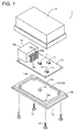
- FIG. 1 is an exploded perspective view of a main configuration of a box-type vehicle-mounted control device according to Example 1 (to Example 9).
- FIG. 2 is a cross-sectional view for describing Example 1.
- the box-type vehicle-mounted control device 1 is configured to include a circuit board 12 and a casing 10 that contains the circuit board 12. On upper/lower (front/back) surfaces of the circuit board 12, electronic components 11, 11, ⁇ including heat generating elements such as an IC and a semiconductor element are mounted by using solder.
- the casing 10 includes a base 13 to which the circuit board 12 is to be fixed, and a box-shaped or lid-shaped cover 14 that has an open lower surface to be assembled to the base 13 so as to cover the circuit board 12.
- the connector 15 On one end of the circuit board 12 in a longitudinal direction, a connector 15 for electrically connecting the circuit board 12 with the outside is attached.
- the connector 15 includes the required number of pin terminals 15a, and a housing 15b.
- the housing 15b has through holes 15c through which the pin terminals 15a are inserted with press-fitting, or the like.
- the pin terminal 15a On the connector 15, the pin terminal 15a is inserted into the through hole 15c of the housing 15b, and then, a lower end portion (couple-bonding portion 15f) of the pin terminal 15a is couple-bonded to the circuit board 12 by using solder in a spot flow process, or the like.
- the base 13 has an overall substantially rectangular plate-like shape so as to close the open lower surface of the cover 14.
- the base 13 includes a rectangular plate-like portion 13a, a rectangular frame-like portion 13b protruding on the rectangular plate-like portion 13a, a pedestal portion 13d that is provided at each of four corners of the rectangular frame-like portion 13b and serves as a seat for the circuit board 12, and a vehicle-mounting fixture 13e extending on an outer periphery of the rectangular plate-like portion 13a.
- the vehicle-mounting fixture 13e is provided to assemble the box-type vehicle-mounted control device 1 to a vehicle body and is fixed to a predetermined position of the vehicle body by engaging with bolts, for example.
- the base 13 and the cover 14 included in the casing 10 of the box-type vehicle-mounted control device 1 are assembled in such a way as to sandwich the circuit board 12 on which the connector 15 is attached. More specifically, the circuit board 12, while being held between the pedestal portion 13d provided at four corners of the base 13 and the cover 14, is fixed with a set screw 17 as an exemplary fastening member.
- a fixing structure for combining the cover 14 and the base 13 is not limited to the above-described structure that is to be screwed and fixed by using the set screw 17.
- the fixing structure may be such that an assembly hole provided at a standing portion that stands from the base 13 and a protruding portion provided at the cover 14 are fittingly fixed or bonded with each other.
- the base 13 and the cover 14 are produced by casting, pressing, cutting, or the like, using a metal material or a resin material. More particularly, the base 13 and the cover 14 are produced by casting, pressing, cutting, or the like, using an alloy composed mainly of aluminum, magnesium, iron, or the like, or using the resin material such as polybutylene terephthalate.
- the cover 14 has a window 14a for the connector 15 to permit the circuit board 12 to receive power supplied from the outside or to exchange input/output signals with an external device through the connector 15.
- circuit board 12 On the circuit board 12, four electronic components 11, 11, ⁇ (three on an upper surface, one on a lower surface) are mounted, for example. Circuit wiring provided on the circuit board 12 is connected to each of the electronic components 11, 11, ⁇ as well as connected to the pin terminal 15a of the connector 15. On the circuit board 12, a thermal via (through hole) 19 is provided at a portion on which the electronic components 11, 11, ⁇ are mounted.
- the thermal via 19 is provided on a lower surface of the electronic component 11 located at the middle of the three electronic components 11, 11, and 11 mounted on an upper surface of the circuit board 12.
- a rectangular protrusion 21 is provided at a position located just below the thermal via 19 on the base 13.
- a high-thermal conductivity layer 20 is provided between a lower surface of the circuit board 12 and an upper surface of the rectangular protrusion 21 on the base 13, so as to contact the lower surface of the circuit board 12 and the upper surface of the rectangular protrusion 21.
- the high-thermal conductivity layer 20 include adhesive, grease, and a heat dissipation sheet.
- the electronic component 11 (main-body portion thereof) positioned at a right end among the three electronic components 11, 11, and 11 mounted on the upper surface of the circuit board 12 is mounted in a state of being spaced from the upper surface of the circuit board 12. In other words, there is a gap between this electronic component 11 and the circuit board 12.
- the heat generated in the electronic components 11, 11, ⁇ is transferred to the base 13 through the thermal via 19 and the high-thermal conductivity layer 20, and dissipated to the atmosphere from the casing 10.
- heat radiating coating layers are formed on specific portions.
- the heat radiating coating layer 31 is formed (applied) on one and/or another surface of the circuit board 12.
- the heat radiating coating layers 32 and 33 are formed (applied) on an inner surface and/or outer surface of the base 13 and the cover 14.
- the heat radiating coating layer 34 is formed (applied) on a portion between the couple-bonding portion 15f on the circuit board 12-side, and a connector housing 15b.
- desirable coating methods include brush coating, spray coating, and dip coating. However, depending on the object to be coated, electrostatic coating, curtain coating, electrostatic coating, or the like may also be employed. As a desirable method for forming a coating film after performing coating with the material may be natural drying, baking, or the like.
- the material forming the heat radiating coating layers (31, 32, 33, and 34) is not particularly limited as long as it is a material having heat radiating property.
- the most desirable material may be the composite material made of organic resin and inorganic particles. In this case, conventionally known inorganic particles may be used without any specific limitation.
- the ceramic powder When blending the ceramic powder, its mean particle size is not particularly limited; still, the desirable size is 0.01 to 200 ⁇ m. If the mean particle size of the ceramic powder is too large, (larger than 200 ⁇ m), a recommended film thickness for allowing efficient heat radiation might be penetrated, possibly leading to a decrease in a bonding strength and an adhesive force. Conversely, if the mean particle size of the ceramic powder is too small (smaller than 0.01 ⁇ m), the ceramic powder might be covered with the organic resin that is a binder, possibly leading to a decrease in heat radiating performance.
- a desirable film thickness of each of the heat radiating coating layers is approximately 1 to 200 ⁇ m. If the film thickness is too large, absorbed heat is easily insulated. If the film thickness is too small, the heat radiating performance tends to decrease. That is, if the film thickness is too large or too small, the amount of heat transfer from the electronic components or the circuit board to the casing (base and cover) is decreased. More desirable film thickness of each of the heat radiating coating layer is 20 to 40 ⁇ m. If the film thickness is larger than 40 ⁇ m, absorbed heat is insulated. If the film thickness if smaller than 20 ⁇ m, heat radiating performance is decreased, and the amount of heat transfer from the electronic components 11, 11, ⁇ and from the circuit board 12 to the casing 10 (the base 13 and the cover 14) is decreased.
- organic resin it is possible to use conventionally known one and is not particularly limited.
- organic resin include synthetic resin and aqueous emulsion resin.
- synthetic resin it is possible to use phenol resin, alkyd resin, melamine urea resin, epoxy resin, polyurethane resin, silicone resin, vinyl acetate resin, acrylic resin, chlorinated rubber resin, vinyl chloride resin, fluororesin, or the like.
- acrylic resin which is inexpensive.
- aqueous emulsion it is possible to use silicone acrylic emulsion, urethane emulsion, acrylic emulsion, or the like.
- Example 1 a first heat radiating coating layer 31 having emissivity of 0.80 or higher is formed on a lower surface (base 13-side) of the circuit board 12 on which the electronic component 11 is mounted, at a portion other than the electronic component 11 and the high-thermal conductivity layer 20.
- a second heat radiating coating layer 32 having emissivity of 0.80 or higher is formed on an inner surface (specifically, a surface facing the first heat radiating coating layer 31) of the base 13.
- the heat radiating coating layer 31 (32) is formed also on an outer periphery of the electronic component 11 mounted on a lower surface of the circuit board 12.
- Example 1 a material containing 45% titanium oxide based on the acrylic resin is employed as the heat radiating coating layers 31 and 32.
- the material has been applied with brush coating to the circuit board 12, heated and dried at 80°C and for 30 minutes so as to achieve a film thickness of 30 ⁇ m.
- Forming the first heat radiating coating layer 31 and the second heat radiating coating layer 32 in this manner increases a high-thermal radiation area.
- the heat generated from the electronic components 11, 11, ⁇ including the heat generating element, as well as the heat transferred to the circuit board 12 is transferred to the first heat radiating coating layer 31 through the circuit board 12 and the thermal via 19.
- the transferred heat is then radiated from the first heat radiating coating layer 31, and absorbed at the second heat radiating coating layer 32 facing the first heat radiating coating layer 31.
- This configuration makes it possible to increase the amount of heat transfer from the electronic components 11, 11, ⁇ and from the circuit board 12 to the base 13 (casing 10).
- the first heat radiating coating layer 31 on the circuit board 12 surface on which no electronic component 11 is mounted, the heat coming from the electronic component 11 is transferred to the first heat radiating coating layer 31 through the thermal via 19. Then, the coating layer 31 radiates the heat. With this configuration, it is possible to promote heat dissipation from the electronic component 11 to the base 13.
- the desirable film thickness of the first heat radiating coating layer 31 and the second heat radiating coating layer 32 is approximately 1 to 200 ⁇ m, and more desirably, 20 to 40 ⁇ m.
- the first heat radiating coating layer 31 and the second heat radiating coating layer 32 may have different compositions.
- the composition is such that each of the coating layers contains a same filler or that the layers are overlapping with each other at 0.5 or higher absorbance in an infrared absorption region at 1200 to 500 cm -1 (wavelength represented in centimeter and then inversed). With such a composition, the heat radiated from the first heat radiating coating layer 31 can be efficiently absorbed by the second heat radiating coating layer 32.
- the heat radiating coating layer 31 be formed in this gap or a back side of the electronic component 11 (the heat radiating coating layer 31 is formed in this gap in Examples 3 and 4 to be described below) .
- the heat generated by the electronic component 11 can be absorbed by the first heat radiating coating layer 31, making it possible to increase the amount of heat transfer to the circuit board 12.
- the first heat radiating coating layer 31 and the second heat radiating coating layer 32 be directly applied to each of base materials.
- the heat radiating coating layer is formed after applying surface treatment such as moisture-proof coating, the film thickness between the surface of the circuit board 12 and the surface of heat radiating coating layer is increased. This decreases the amount of heat transfer, lowering heat dissipation property.
- the portion for forming the first heat radiating coating layer 31 and the second heat radiating coating layer 32 is not limited to an entire surface of each of the surfaces.
- the heat radiating coating layers 31 and 32 may be formed at one portion, specifically at heat-generating components and their surroundings. This can decrease the amount of use of a coating material for forming the coating layers 31 and 32.
- a heat dissipation fin on an outer surface of the base 13 on an inner surface of which the second heat radiating coating layer 32 is provided makes it easier to dissipate to the atmosphere the heat absorbed by the casing 10 from the circuit board 12 and the electronic component 11.
- roughening surface conditions forming minute irregularities, or the like
- roughening surface conditions forming minute irregularities, or the like
- This increases the amount of heat transfer of the first heat radiating coating layer 31 and the second heat radiating coating layer 32 and improves heat dissipation property.
- the first heat radiating coating layer 31 having emissivity of 0.80 or higher is formed on a surface of a surface (base 13-side) that is not facing a heat source 50 (vehicle-mounted engine, for example) on the circuit board 12.
- the second heat radiating coating layer 32 having emissivity of 0.80 or higher is formed on an inner surface (specifically, an upper surface facing the first heat radiating coating layer 31) of the base 13.
- a third heat radiating coating layer 33 having emissivity of 0.80 or higher is formed on an outer surface (lower surface) of the base 13 on the inner surface of which the second heat radiating coating layer 32 is formed.
- Example 2 with this configuration, no heat radiating coating layer is formed on a heat source 50-side (upper surface of the circuit board 12 and inner/outer surface of the cover 14). This makes it possible to suppress absorption of the heat emitted from the heat source 50 and to radiate the heat transferred to the base 13 through the first heat radiating coating layer 31 and the second heat radiating coating layer 32 to the atmosphere at the third heat radiating coating layer 33.
- This configuration compared with Example 1, can increase the amount of heat transfer from the circuit board 12 and the electronic component 11 to the atmosphere. As a result, heat dissipation property of the box-type vehicle-mounted control device 1 can be improved. As a result, this configuration can further suppress the temperature to a lower level inside the casing 10 of the box-type vehicle-mounted control device 1 including the electronic components 11, 11, ⁇ and enhance reliability of the device.
- compositions of the first heat radiating coating layer 31, the second heat radiating coating layer 32, and the third heat radiating coating layer 33 may differ from each other. Still, it is desirable that the composition be such that each of the coating layers contains a same filler or that the layers are overlapping with each other at 0.5 or higher absorbance in an infrared absorption region at 1200 to 500 cm -1 .
- This configuration makes it possible for the second heat radiating coating layer 32 to efficiently absorb the heat radiated from the first heat radiating coating layer 31, and for the third heat radiating coating layer 33 to dissipate the heat. Accordingly, heat dissipation property is improved.
- Specification including the film thickness of the third heat radiating coating layer 33 is similar to specification of the first heat radiating coating layer 31 and of the second heat radiating coating layer 32.
- the desirable film thickness is approximately 1 to 200 ⁇ m, and more desirably, 20 to 40 ⁇ m. If the film thickness is too large, the absorbed heat is insulated. If the film thickness is too small, heat radiating performance is lowered and the amount of heat transfer from the base 13 to the atmosphere is decreased. Roughening the surface condition of the third heat radiating coating layer 33 (forming minute irregularities, or the like) increases the surface area of the coating layer 33 and further improves heat dissipation property.
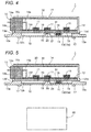
- Example 3 as illustrated in FIG. 4 , the first heat radiating coating layer 31 having emissivity of 0.80 or higher is formed on a surface (upper surface) of the cover 14 of the circuit board 12 on which the electronic component 11 is mounted.
- the second heat radiating coating layer 32 having emissivity of 0.80 or higher is formed on an inner surface (specifically, a lower surface facing the first heat radiating coating layer 31) of the cover 14.
- the first heat radiating coating layer 31 is formed so as to cover the electronic components 11, 11, and 11 mounted on an upper surface of the circuit board 12. Between the electronic component 11 located at a right end and the circuit board 12, a gap is formed. It is configured such that the first heat radiating coating layer 31 fills this gap.
- Forming the first heat radiating coating layer 31 and the second heat radiating coating layer 32 in this manner increases a high-thermal radiation area.
- the heat generated from the electronic components 11, 11, ⁇ including the heat generating element as well as the heat transferred to the circuit board 12 is then transferred to the first heat radiating coating layer 31 and radiated from the first heat radiating coating layer 31, and then, is absorbed at the second heat radiating coating layer 32 that is a facing surface. Accordingly, it is possible to increase the amount of heat transfer from the electronic components 11, 11, ⁇ and from the circuit board 12 to the cover 14 (casing 10).
- heat dissipation property of the box-type vehicle-mounted control device 1 can be improved. This configuration can suppress the temperature to a low level inside the casing 10 of the box-type vehicle-mounted control device 1, including the electronic components 11, 11, ⁇ and enhance reliability of the device.
- the first heat radiating coating layer 31 on the circuit board 12 surface on which no electronic component 11 is mounted, the heat coming from the electronic component 11 is transferred to the first heat radiating coating layer 31 through the thermal via 19. Then, the coating layer 31 radiates the heat. With this configuration, it is possible to promote heat dissipation from the electronic component 11 to the cover 14.
- a heat dissipation fin on an outer surface of the cover 14 on an inner surface of which the second heat radiating coating layer 32 is provided makes it easier to dissipate to the atmosphere the heat absorbed by the casing from the circuit board 12 and the electronic component 11.
- roughening surface conditions forming minute irregularities, or the like
- roughening surface conditions forming minute irregularities, or the like
- This increases the amount of heat transfer of the first heat radiating coating layer 31 and the second heat radiating coating layer 32 and improves heat dissipation property.
- first heat radiating coating layer 31 and the second heat radiating coating layer 32 are the same as the specifications, or the like, of the above-described Examples 1 and 2, and thus will be omitted.
- Example 4 as illustrated in FIG. 5 , the first heat radiating coating layer 31 having emissivity of 0.80 or higher is formed on a surface on (cover 14-side) that is not facing the heat source 50 (vehicle-mounted engine, for example) on the circuit board 12.
- the second heat radiating coating layer 32 having emissivity of 0.80 or higher is formed on an inner surface (specifically, a lower surface facing the first heat radiating coating layer 31) of the cover 14.
- the third heat radiating coating layer 33 having emissivity of 0.80 or higher is formed on an outer surface (upper surface) of the cover 14 on an inner surface of which the second heat radiating coating layer 32 is formed.
- Example 4 with this configuration, the heat radiating coating layer is not formed on the heat source 50-side (lower surface of the circuit board 12 and inner/outer surface of the base 13). This makes it possible to suppress absorption of the heat emitted from the heat source 50 and to radiate the heat transferred to the cover 14 through the first heat radiating coating layer 31 and the second heat radiating coating layer 32 to the atmosphere at the third heat radiating coating layer 33.
- This configuration compared with Example 3, enables further increasing the amount of heat transfer from the circuit board 12 and the electronic component 11 to the atmosphere. As a result, heat dissipation property of the box-type vehicle-mounted control device 1 can be further improved.
- This configuration can further suppress the temperature to a lower level inside the casing 10 of the box-type vehicle-mounted control device 1 including the electronic components 11, 11, ⁇ and enhance reliability of the device.
- first heat radiating coating layer 31 and the second heat radiating coating layer 32 and the third heat radiating coating layer 33 are the same as the specifications, or the like of the above-described Examples 1, 2, and 3, and thus will be omitted.
- Example 5 will be described focusing on a difference from the Examples 1 to 4.
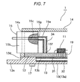
- Example 5 as illustrated in FIGS. 6 and 7 , similarly to Example 1, the first heat radiating coating layer 31 and the second heat radiating coating layer 32 are formed.
- a fourth heat radiating coating layer 34 having emissivity of 0.80 or higher is formed on the pin terminal 15a of the connector 15 so as to cover an entire periphery of a portion ranging from the circuit board 12-side couple-bonding portion 15f to the connector housing 15b.
- the fourth heat radiating coating layer 34 need not be applied to entire portions (entire periphery, entire length) of the pin terminal 15a. Accordingly, it is possible to decrease the amount of use of the coating material.
- the fourth heat radiating coating layer 34 is formed so as to fill a portion between the pin terminal 15a and the through hole 15c of the housing 15b to which the pin terminal 15a is attached.
- the fourth heat radiating coating layer 34 is formed so as to seal a minute gap portion 15g formed between an inner end portion of each of the through holes 15c and each of the pin terminals 15a (coating is applied so as to cover the gap portion 15g by forming the film thickness of the fourth heat radiating coating layer 34 to be thicker than the gap portion 15g, or by any other method).
- the fourth heat radiating coating layer 34 is similar to the specifications of the first, the second, and the third heat radiating coating layers 31, 32, and 33.
- the desirable film thickness is approximately 1 to 200 ⁇ m, more desirably, 20 to 40 ⁇ m.
- compositions of the first heat radiating coating layer 31, the second heat radiating coating layer 32, and the fourth heat radiating coating layer 34 may differ from each other. Still, it is desirable that the compositions be such that each of the coating layers contains a same filler or that the layers are overlapping with each other at 0.5 or higher absorbance in an infrared absorption region at 1200 to 500 cm -1 .
- the heat radiated from the first heat radiating coating layer 31 can be efficiently absorbed by the second heat radiating coating layer 32 and the fourth heat radiating coating layer 34. Accordingly, heat dissipation property is improved.
- roughening the surface condition of the fourth heat radiating coating layer 34 increases the surface area of the coating layer 34 and improves heat absorbing property.
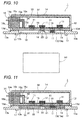
- each of Examples 6, 7, 8, and 9, as illustrated in FIGS. 8, 9 , 10, and 11 has a configuration of each of Examples 2, 3, 4, and a combination of Examples 1 and 3, as a base.
- each of Examples 6, 7, 8, and 9 has a configuration in which the fourth heat radiating coating layer 34 having emissivity of 0.80 or higher is formed on the pin terminal 15a of the connector 15 so as to cover a portion ranging from the couple-bonding portion 15f joined with the circuit board 12, to the connector housing 15b.
- Comparative Example 1 is, as illustrated in FIG. 12 , has a configuration in which none of the heat radiating coating layers (31, 32, 33, and 34) is formed in the box-type vehicle-mounted control device 1. Accordingly, the amount of heat transfer of the heat generated at the electronic component 11 including a heat generating element and the amount of the heat transferred to the circuit board 12 are small, resulting in insufficient heat dissipation property.
- Comparative Example 2 is, as illustrated in FIG. 13 , has a configuration in which the first heat radiating coating layer 31 is formed only on one surface (lower surface) of the circuit board 12 of the box-type vehicle-mounted control device 1. Accordingly, although the heat generated at the electronic component 11 including the heat generating element as well as the heat transferred to the circuit board 12 is radiated, no heat absorption on a facing surface can be expected.
- Table 1 illustrates configurations and heat dissipation effects of the box-type vehicle-mounted control device 1 for Examples 1, 2, 5, and 6, and for Comparative Examples 1 and 2. According to Table 1, it is understandable that, when the heat radiating coating layers 31, 32, 33, and 34 are formed at specific portions of the circuit board 12, the base 13, the cover 14, and the pin terminal 15a of the connector 15, the amount of heat transfer of the heat generated at the electronic component 11 including the heat generating element as well as of the heat transferred to the circuit board 12 is increased, leading to improvement of heat dissipation property.
Landscapes
- Engineering & Computer Science (AREA)
- Microelectronics & Electronic Packaging (AREA)
- Physics & Mathematics (AREA)
- Thermal Sciences (AREA)
- Cooling Or The Like Of Electrical Apparatus (AREA)
- Coupling Device And Connection With Printed Circuit (AREA)
- Non-Metallic Protective Coatings For Printed Circuits (AREA)
- Structure Of Printed Boards (AREA)
- Casings For Electric Apparatus (AREA)
Abstract
Description
- The present invention relates to a box-type vehicle-mounted control device equipped with a circuit board on which an electronic components are mounted, a base to which the circuit board is fixed, and a cover assembled to the base so as to cover the circuit board, and particularly relates to the box-type vehicle-mounted control device configured to be capable of improving heat dissipation property.
- Conventionally, a box-type vehicle-mounted control device (box-type electronic module) mounted on an automobile typically includes a circuit board on which the electronic components including a heat generating element such as a semiconductor element are mounted, and a casing that contains the circuit board. In this configuration, the casing typically includes a base to which the circuit board is fixed, and a cover assembled to the base to cover the circuit board.
- In such a box-type vehicle-mounted control device, a recent trend of miniaturization and multi-functionality due to space restriction has increased the amount of heat generation. Therefore, as disclosed in
PTL 1, for example, in order to transfer the heat generated in the electronic components (heat generating elements) to the casing and to dissipate the heat at an outer surface of the casing to the atmosphere, applying surface treatment to the casing has been proposed. - Also in PTL 2, to suppress an occurrence of a crack in the vicinity of a connector attached to the circuit board, applying surface treatment to the circuit board is proposed.
-
- PTL 1:
JP 2004-304200 A - PTL 2:
JP 2012-204729 A - Meanwhile, in recent years, there is a social demand for an engine room that can achieve high-density and miniaturization from a viewpoint of resource saving, or the like. Miniaturization has been promoted also in the box-type vehicle-mounted control device. This also promotes reduction in a substrate area and integration of the electronic components, and thus increases heat generation density, leading to a desire to achieve further improvement in heat dissipation property.
- A conventional technique that has been proposed has a structure in which heat is absorbed from the heat generating element by using surface treatment applied to a surface of the casing. With this structure, however, the amount of heat transfer from the circuit board and the heat generating element to the casing is too small to sufficiently perform heat absorption.
- In view of the above-described situation, the present invention is intended to provide a box-type vehicle-mounted control device with excellent heat dissipation property and that can effectively increase the amount of heat transfer from the electronic components and the circuit board to the casing (base or cover).
- To achieve the above object, a box-type vehicle-mounted control device according to the present invention fundamentally includes a circuit board on which electronic components are mounted, a base to which the circuit board is fixed, and a cover assembled to the base so as to cover the circuit board.
- On the box-type vehicle-mounted control device, a first heat radiating coating layer is formed on at least one surface of the circuit board, and a second heat radiating coating layer is formed on an inner surface of one or both of the base and the cover facing the first heat radiating coating layer.
- The material forming the heat radiating coating layer used in the box-type vehicle-mounted control device according to the present invention is not particularly limited as long as it is a material having heat radiating property. Still, the most desirable material is a composite material made of organic resin and inorganic particles. In this case, conventionally known inorganic particles may be used without any specific limitation. Still, it is desirable to blend at least one of ceramic powders, or the like, of aluminum oxide, magnesium oxide, titanium oxide, zirconia, iron oxide, copper oxide, nickel oxide, cobalt oxide, lithium oxide, zinc oxide, silicon dioxide, or the like, listed as desirable examples.
- According the present invention, at least two heat radiating coating layers are formed. This configuration increases a high-thermal radiation area. In addition, the heat generated from electronic components including heat generating elements as well as the heat that has been transferred to the circuit board can be radiated at one heat radiating coating layer, and the heat can then be absorbed at another heat radiating coating layer formed so as to face the one heat radiating coating layer. This configuration makes it possible to increase the amount of heat transfer from the electronic component and the circuit board to the casing. Accordingly, it is possible to improve heat dissipation property of the box-type vehicle-mounted control device. This improvement can suppress a temperature to a low level inside the casing of the box-type vehicle-mounted control device, including electronic components (heat generating elements) and enhance reliability of the device.
- Problems, configurations, and effects other than in the above description will be clarified by the following embodiments.
-
- [
FIG. 1] FIG. 1 is an exploded perspective view of a basic configuration of a box-type vehicle-mounted control device according to embodiments (Examples 1 to 9) of the present invention. - [
FIG. 2] FIG. 2 is a cross-sectional view for describing Example 1. - [
FIG. 3] FIG. 3 is a cross-sectional view for describing Example 2. - [
FIG. 4] FIG. 4 is a cross-sectional view for describing Example 3. - [
FIG. 5] FIG. 5 is a cross-sectional view for describing Example 4. - [
FIG. 6] FIG. 6 is a cross-sectional view for describing Example 5. - [
FIG. 7] FIG. 7 is a cutaway enlarged sectional view of a portion around a connector illustrated inFIG. 6 . - [
FIG. 8] FIG. 8 is a cross-sectional view for describing Example 6. - [
FIG. 9] FIG. 9 is a cross-sectional view for describing Example 7. - [
FIG. 10] FIG. 10 is a cross-sectional view for describing Example 8. - [
FIG. 11] FIG. 11 is a cross-sectional view for describing Example 9. - [
FIG. 12] FIG. 12 is a cross-sectional view for describing Comparative Example 1. - [
FIG. 13] FIG. 13 is a cross-sectional view for describing Comparative Example 2. - Hereinafter, embodiments of the present invention will be described with reference to the drawings.
-
FIGS. 1 to 11 are diagrams for describing embodiments (Examples 1 to 9) of the box-type vehicle-mounted control device according to the present invention. In each of the diagrams, portions with same configurations, same functions, or with corresponding relationship with each other are indicated by same or related reference signs. To facilitate understanding of the invention,FIGS. 1 to 11 include exaggerated drawings related to the thicknesses of individual portions, or the like (in particular, the film thicknesses of the heat radiating coating layers). -
FIG. 1 is an exploded perspective view of a main configuration of a box-type vehicle-mounted control device according to Example 1 (to Example 9).FIG. 2 is a cross-sectional view for describing Example 1. - The box-type vehicle-mounted
control device 1 is configured to include acircuit board 12 and acasing 10 that contains thecircuit board 12. On upper/lower (front/back) surfaces of thecircuit board 12,electronic components casing 10 includes abase 13 to which thecircuit board 12 is to be fixed, and a box-shaped or lid-shaped cover 14 that has an open lower surface to be assembled to thebase 13 so as to cover thecircuit board 12. - On one end of the
circuit board 12 in a longitudinal direction, aconnector 15 for electrically connecting thecircuit board 12 with the outside is attached. Theconnector 15 includes the required number ofpin terminals 15a, and ahousing 15b. Thehousing 15b has throughholes 15c through which thepin terminals 15a are inserted with press-fitting, or the like. On theconnector 15, thepin terminal 15a is inserted into thethrough hole 15c of thehousing 15b, and then, a lower end portion (couple-bonding portion 15f) of thepin terminal 15a is couple-bonded to thecircuit board 12 by using solder in a spot flow process, or the like. - The
base 13 has an overall substantially rectangular plate-like shape so as to close the open lower surface of thecover 14. Specifically, thebase 13 includes a rectangular plate-like portion 13a, a rectangular frame-like portion 13b protruding on the rectangular plate-like portion 13a, apedestal portion 13d that is provided at each of four corners of the rectangular frame-like portion 13b and serves as a seat for thecircuit board 12, and a vehicle-mounting fixture 13e extending on an outer periphery of the rectangular plate-like portion 13a. The vehicle-mountingfixture 13e is provided to assemble the box-type vehicle-mountedcontrol device 1 to a vehicle body and is fixed to a predetermined position of the vehicle body by engaging with bolts, for example. - The
base 13 and thecover 14 included in thecasing 10 of the box-type vehicle-mountedcontrol device 1 are assembled in such a way as to sandwich thecircuit board 12 on which theconnector 15 is attached. More specifically, thecircuit board 12, while being held between thepedestal portion 13d provided at four corners of thebase 13 and thecover 14, is fixed with aset screw 17 as an exemplary fastening member. - A fixing structure for combining the
cover 14 and thebase 13 is not limited to the above-described structure that is to be screwed and fixed by using theset screw 17. For example, the fixing structure may be such that an assembly hole provided at a standing portion that stands from thebase 13 and a protruding portion provided at thecover 14 are fittingly fixed or bonded with each other. - The
base 13 and thecover 14 are produced by casting, pressing, cutting, or the like, using a metal material or a resin material. More particularly, thebase 13 and thecover 14 are produced by casting, pressing, cutting, or the like, using an alloy composed mainly of aluminum, magnesium, iron, or the like, or using the resin material such as polybutylene terephthalate. - The
cover 14 has awindow 14a for theconnector 15 to permit thecircuit board 12 to receive power supplied from the outside or to exchange input/output signals with an external device through theconnector 15. - On the
circuit board 12, fourelectronic components circuit board 12 is connected to each of theelectronic components pin terminal 15a of theconnector 15. On thecircuit board 12, a thermal via (through hole) 19 is provided at a portion on which theelectronic components - On a lower surface of the
electronic component 11 located at the middle of the threeelectronic components circuit board 12, the thermal via 19 is provided. In addition, at a position located just below the thermal via 19 on thebase 13, arectangular protrusion 21 is provided. Between a lower surface of thecircuit board 12 and an upper surface of therectangular protrusion 21 on thebase 13, a high-thermal conductivity layer 20 is provided so as to contact the lower surface of thecircuit board 12 and the upper surface of therectangular protrusion 21. Herein, examples of the high-thermal conductivity layer 20 include adhesive, grease, and a heat dissipation sheet. - Furthermore, the electronic component 11 (main-body portion thereof) positioned at a right end among the three
electronic components circuit board 12 is mounted in a state of being spaced from the upper surface of thecircuit board 12. In other words, there is a gap between thiselectronic component 11 and thecircuit board 12. - In the box-type vehicle-mounted
control device 1 with the above-described configuration, the heat generated in theelectronic components thermal conductivity layer 20, and dissipated to the atmosphere from thecasing 10. - In each of Examples (1 to 9), heat radiating coating layers (31, 32, 33, and 34) are formed on specific portions. In this case, after the
electronic component 11 and theconnector 15 have been mounted on thecircuit board 12, the heat radiatingcoating layer 31 is formed (applied) on one and/or another surface of thecircuit board 12. Furthermore, after thebase 13 and thecover 14 have been produced to have a predetermined size and form, the heat radiating coating layers 32 and 33 are formed (applied) on an inner surface and/or outer surface of thebase 13 and thecover 14. Furthermore, on thepin terminal 15a of theconnector 15, the heat radiatingcoating layer 34 is formed (applied) on a portion between the couple-bonding portion 15f on the circuit board 12-side, and aconnector housing 15b. - Examples of desirable coating methods include brush coating, spray coating, and dip coating. However, depending on the object to be coated, electrostatic coating, curtain coating, electrostatic coating, or the like may also be employed. As a desirable method for forming a coating film after performing coating with the material may be natural drying, baking, or the like.
- The material forming the heat radiating coating layers (31, 32, 33, and 34) is not particularly limited as long as it is a material having heat radiating property. Still, the most desirable material may be the composite material made of organic resin and inorganic particles. In this case, conventionally known inorganic particles may be used without any specific limitation. Still, it is desirable to blend at least one of ceramic powders, or the like, of aluminum oxide, magnesium oxide, titanium oxide, zirconia, iron oxide, copper oxide, nickel oxide, cobalt oxide, lithium oxide, zinc oxide, silicon dioxide, or the like, listed as desirable examples.
- When blending the ceramic powder, its mean particle size is not particularly limited; still, the desirable size is 0.01 to 200 µm. If the mean particle size of the ceramic powder is too large, (larger than 200 µm), a recommended film thickness for allowing efficient heat radiation might be penetrated, possibly leading to a decrease in a bonding strength and an adhesive force. Conversely, if the mean particle size of the ceramic powder is too small (smaller than 0.01 µm), the ceramic powder might be covered with the organic resin that is a binder, possibly leading to a decrease in heat radiating performance.
- In addition, a desirable film thickness of each of the heat radiating coating layers is approximately 1 to 200 µm. If the film thickness is too large, absorbed heat is easily insulated. If the film thickness is too small, the heat radiating performance tends to decrease. That is, if the film thickness is too large or too small, the amount of heat transfer from the electronic components or the circuit board to the casing (base and cover) is decreased. More desirable film thickness of each of the heat radiating coating layer is 20 to 40 µm. If the film thickness is larger than 40 µm, absorbed heat is insulated. If the film thickness if smaller than 20 µm, heat radiating performance is decreased, and the amount of heat transfer from the
electronic components circuit board 12 to the casing 10 (thebase 13 and the cover 14) is decreased. - As the organic resin, it is possible to use conventionally known one and is not particularly limited. Examples of organic resin include synthetic resin and aqueous emulsion resin. As the synthetic resin, it is possible to use phenol resin, alkyd resin, melamine urea resin, epoxy resin, polyurethane resin, silicone resin, vinyl acetate resin, acrylic resin, chlorinated rubber resin, vinyl chloride resin, fluororesin, or the like. Among these, the most desirable synthetic resin is acrylic resin, which is inexpensive. As the aqueous emulsion, it is possible to use silicone acrylic emulsion, urethane emulsion, acrylic emulsion, or the like.
- Next, Examples 1 to 9 will be described in sequence.
- In Example 1, as illustrated in
FIG. 2 , a first heat radiatingcoating layer 31 having emissivity of 0.80 or higher is formed on a lower surface (base 13-side) of thecircuit board 12 on which theelectronic component 11 is mounted, at a portion other than theelectronic component 11 and the high-thermal conductivity layer 20. In addition, a second heat radiatingcoating layer 32 having emissivity of 0.80 or higher is formed on an inner surface (specifically, a surface facing the first heat radiating coating layer 31) of thebase 13. The heat radiating coating layer 31 (32) is formed also on an outer periphery of theelectronic component 11 mounted on a lower surface of thecircuit board 12. - In Example 1, a material containing 45% titanium oxide based on the acrylic resin is employed as the heat radiating coating layers 31 and 32. The material has been applied with brush coating to the
circuit board 12, heated and dried at 80°C and for 30 minutes so as to achieve a film thickness of 30 µm. - Forming the first heat radiating
coating layer 31 and the second heat radiatingcoating layer 32 in this manner increases a high-thermal radiation area. In addition, the heat generated from theelectronic components circuit board 12, is transferred to the first heat radiatingcoating layer 31 through thecircuit board 12 and the thermal via 19. The transferred heat is then radiated from the first heat radiatingcoating layer 31, and absorbed at the second heat radiatingcoating layer 32 facing the first heat radiatingcoating layer 31. This configuration makes it possible to increase the amount of heat transfer from theelectronic components circuit board 12 to the base 13 (casing 10). - Accordingly, it is possible to improve heat dissipation property of the box-type vehicle-mounted
control device 1. This improvement can suppress the temperature to a low level inside thecasing 10 of the box-type vehicle-mountedcontrol device 1, including anelectronic components - Moreover, by forming the first heat radiating
coating layer 31 on thecircuit board 12 surface on which noelectronic component 11 is mounted, the heat coming from theelectronic component 11 is transferred to the first heat radiatingcoating layer 31 through the thermal via 19. Then, thecoating layer 31 radiates the heat. With this configuration, it is possible to promote heat dissipation from theelectronic component 11 to thebase 13. - The desirable film thickness of the first heat radiating
coating layer 31 and the second heat radiatingcoating layer 32 is approximately 1 to 200 µm, and more desirably, 20 to 40 µm. - The first heat radiating
coating layer 31 and the second heat radiatingcoating layer 32 may have different compositions. Desirably, the composition is such that each of the coating layers contains a same filler or that the layers are overlapping with each other at 0.5 or higher absorbance in an infrared absorption region at 1200 to 500 cm-1 (wavelength represented in centimeter and then inversed). With such a composition, the heat radiated from the first heat radiatingcoating layer 31 can be efficiently absorbed by the second heat radiatingcoating layer 32. - In a case where the
electronic component 11 has been mounted (theelectronic component 11 at a right end inFIG. 2 ) while there is a gap between theelectronic component 11 and thecircuit board 12, it is desirable that the heat radiatingcoating layer 31 be formed in this gap or a back side of the electronic component 11 (the heat radiatingcoating layer 31 is formed in this gap in Examples 3 and 4 to be described below) . With this configuration, the heat generated by theelectronic component 11 can be absorbed by the first heat radiatingcoating layer 31, making it possible to increase the amount of heat transfer to thecircuit board 12. - It is desirable that the first heat radiating
coating layer 31 and the second heat radiatingcoating layer 32 be directly applied to each of base materials. On thecircuit board 12, for example, if the heat radiating coating layer is formed after applying surface treatment such as moisture-proof coating, the film thickness between the surface of thecircuit board 12 and the surface of heat radiating coating layer is increased. This decreases the amount of heat transfer, lowering heat dissipation property. - The portion for forming the first heat radiating
coating layer 31 and the second heat radiatingcoating layer 32 is not limited to an entire surface of each of the surfaces. The heat radiating coating layers 31 and 32 may be formed at one portion, specifically at heat-generating components and their surroundings. This can decrease the amount of use of a coating material for forming the coating layers 31 and 32. - Moreover, providing a heat dissipation fin on an outer surface of the base 13 on an inner surface of which the second heat radiating
coating layer 32 is provided, makes it easier to dissipate to the atmosphere the heat absorbed by thecasing 10 from thecircuit board 12 and theelectronic component 11. - In addition, roughening surface conditions (forming minute irregularities, or the like) on the first heat radiating
coating layer 31 and the second heat radiatingcoating layer 32 increases the surface areas of the coating layers 31 and 32. This increases the amount of heat transfer of the first heat radiatingcoating layer 31 and the second heat radiatingcoating layer 32 and improves heat dissipation property. - In Example 2, as illustrated in
FIG. 3 , the first heat radiatingcoating layer 31 having emissivity of 0.80 or higher is formed on a surface of a surface (base 13-side) that is not facing a heat source 50 (vehicle-mounted engine, for example) on thecircuit board 12. In addition, the second heat radiatingcoating layer 32 having emissivity of 0.80 or higher is formed on an inner surface (specifically, an upper surface facing the first heat radiating coating layer 31) of thebase 13. Furthermore, a third heat radiatingcoating layer 33 having emissivity of 0.80 or higher is formed on an outer surface (lower surface) of the base 13 on the inner surface of which the second heat radiatingcoating layer 32 is formed. - In Example 2 with this configuration, no heat radiating coating layer is formed on a heat source 50-side (upper surface of the
circuit board 12 and inner/outer surface of the cover 14). This makes it possible to suppress absorption of the heat emitted from theheat source 50 and to radiate the heat transferred to the base 13 through the first heat radiatingcoating layer 31 and the second heat radiatingcoating layer 32 to the atmosphere at the third heat radiatingcoating layer 33. - This configuration, compared with Example 1, can increase the amount of heat transfer from the
circuit board 12 and theelectronic component 11 to the atmosphere. As a result, heat dissipation property of the box-type vehicle-mountedcontrol device 1 can be improved. As a result, this configuration can further suppress the temperature to a lower level inside thecasing 10 of the box-type vehicle-mountedcontrol device 1 including theelectronic components - Compositions of the first heat radiating
coating layer 31, the second heat radiatingcoating layer 32, and the third heat radiatingcoating layer 33 may differ from each other. Still, it is desirable that the composition be such that each of the coating layers contains a same filler or that the layers are overlapping with each other at 0.5 or higher absorbance in an infrared absorption region at 1200 to 500 cm-1. This configuration makes it possible for the second heat radiatingcoating layer 32 to efficiently absorb the heat radiated from the first heat radiatingcoating layer 31, and for the third heat radiatingcoating layer 33 to dissipate the heat. Accordingly, heat dissipation property is improved. - Specification including the film thickness of the third heat radiating
coating layer 33 is similar to specification of the first heat radiatingcoating layer 31 and of the second heat radiatingcoating layer 32. The desirable film thickness is approximately 1 to 200 µm, and more desirably, 20 to 40 µm. If the film thickness is too large, the absorbed heat is insulated. If the film thickness is too small, heat radiating performance is lowered and the amount of heat transfer from the base 13 to the atmosphere is decreased. Roughening the surface condition of the third heat radiating coating layer 33 (forming minute irregularities, or the like) increases the surface area of thecoating layer 33 and further improves heat dissipation property. - In Example 3, as illustrated in
FIG. 4 , the first heat radiatingcoating layer 31 having emissivity of 0.80 or higher is formed on a surface (upper surface) of thecover 14 of thecircuit board 12 on which theelectronic component 11 is mounted. In addition, the second heat radiatingcoating layer 32 having emissivity of 0.80 or higher is formed on an inner surface (specifically, a lower surface facing the first heat radiating coating layer 31) of thecover 14. Herein, the first heat radiatingcoating layer 31 is formed so as to cover theelectronic components circuit board 12. Between theelectronic component 11 located at a right end and thecircuit board 12, a gap is formed. It is configured such that the first heat radiatingcoating layer 31 fills this gap. - Forming the first heat radiating
coating layer 31 and the second heat radiatingcoating layer 32 in this manner increases a high-thermal radiation area. In addition, the heat generated from theelectronic components circuit board 12 is then transferred to the first heat radiatingcoating layer 31 and radiated from the first heat radiatingcoating layer 31, and then, is absorbed at the second heat radiatingcoating layer 32 that is a facing surface. Accordingly, it is possible to increase the amount of heat transfer from theelectronic components circuit board 12 to the cover 14 (casing 10). As a result, heat dissipation property of the box-type vehicle-mountedcontrol device 1 can be improved. This configuration can suppress the temperature to a low level inside thecasing 10 of the box-type vehicle-mountedcontrol device 1, including theelectronic components - Moreover, by forming the first heat radiating
coating layer 31 on thecircuit board 12 surface on which noelectronic component 11 is mounted, the heat coming from theelectronic component 11 is transferred to the first heat radiatingcoating layer 31 through the thermal via 19. Then, thecoating layer 31 radiates the heat. With this configuration, it is possible to promote heat dissipation from theelectronic component 11 to thecover 14. - Moreover, providing a heat dissipation fin on an outer surface of the
cover 14 on an inner surface of which the second heat radiatingcoating layer 32 is provided, makes it easier to dissipate to the atmosphere the heat absorbed by the casing from thecircuit board 12 and theelectronic component 11. - In addition, roughening surface conditions (forming minute irregularities, or the like) on the first heat radiating
coating layer 31 and the second heat radiatingcoating layer 32 increases the surface areas of the coating layers 31 and 32. This increases the amount of heat transfer of the first heat radiatingcoating layer 31 and the second heat radiatingcoating layer 32 and improves heat dissipation property. - Specifications, or the like, of the first heat radiating
coating layer 31 and the second heat radiatingcoating layer 32 are the same as the specifications, or the like, of the above-described Examples 1 and 2, and thus will be omitted. - In Example 4, as illustrated in
FIG. 5 , the first heat radiatingcoating layer 31 having emissivity of 0.80 or higher is formed on a surface on (cover 14-side) that is not facing the heat source 50 (vehicle-mounted engine, for example) on thecircuit board 12. In addition, the second heat radiatingcoating layer 32 having emissivity of 0.80 or higher is formed on an inner surface (specifically, a lower surface facing the first heat radiating coating layer 31) of thecover 14. Furthermore, the third heat radiatingcoating layer 33 having emissivity of 0.80 or higher is formed on an outer surface (upper surface) of thecover 14 on an inner surface of which the second heat radiatingcoating layer 32 is formed. - In Example 4 with this configuration, the heat radiating coating layer is not formed on the heat source 50-side (lower surface of the
circuit board 12 and inner/outer surface of the base 13). This makes it possible to suppress absorption of the heat emitted from theheat source 50 and to radiate the heat transferred to thecover 14 through the first heat radiatingcoating layer 31 and the second heat radiatingcoating layer 32 to the atmosphere at the third heat radiatingcoating layer 33. - This configuration, compared with Example 3, enables further increasing the amount of heat transfer from the
circuit board 12 and theelectronic component 11 to the atmosphere. As a result, heat dissipation property of the box-type vehicle-mountedcontrol device 1 can be further improved. This configuration can further suppress the temperature to a lower level inside thecasing 10 of the box-type vehicle-mountedcontrol device 1 including theelectronic components - Specifications, or the like, of the first heat radiating
coating layer 31 and the second heat radiatingcoating layer 32 and the third heat radiatingcoating layer 33 are the same as the specifications, or the like of the above-described Examples 1, 2, and 3, and thus will be omitted. - Example 5 will be described focusing on a difference from the Examples 1 to 4. In Example 5, as illustrated in
FIGS. 6 and7 , similarly to Example 1, the first heat radiatingcoating layer 31 and the second heat radiatingcoating layer 32 are formed. In addition, a fourth heat radiatingcoating layer 34 having emissivity of 0.80 or higher is formed on thepin terminal 15a of theconnector 15 so as to cover an entire periphery of a portion ranging from the circuit board 12-side couple-bonding portion 15f to theconnector housing 15b. - With this configuration, the heat transferred from the
electronic components circuit board 12 to thepin terminal 15a is absorbed at the fourth heat radiatingcoating layer 34. This heat is then transferred from thepin terminal 15a to an external connector (not illustrated) and then dissipated to the outside of thecasing 10. This configuration, compared with Example 1, enables further increasing the amount of heat transfer from thecircuit board 12 and theelectronic component 11 to the outside (to the atmosphere). As a result, heat dissipation property of the box-type vehicle-mountedcontrol device 1 can be further improved. This configuration can further suppress the temperature to a lower level inside thecasing 10 of the box-type vehicle-mountedcontrol device 1 including theelectronic components - The fourth heat radiating
coating layer 34 need not be applied to entire portions (entire periphery, entire length) of thepin terminal 15a. Accordingly, it is possible to decrease the amount of use of the coating material. - In one desirable aspect, as illustrated in
FIG. 7 , the fourth heat radiatingcoating layer 34 is formed so as to fill a portion between thepin terminal 15a and the throughhole 15c of thehousing 15b to which thepin terminal 15a is attached. In other words, the fourth heat radiatingcoating layer 34 is formed so as to seal aminute gap portion 15g formed between an inner end portion of each of the throughholes 15c and each of thepin terminals 15a (coating is applied so as to cover thegap portion 15g by forming the film thickness of the fourth heat radiatingcoating layer 34 to be thicker than thegap portion 15g, or by any other method). By sealing the portion between thepin terminal 15a and the throughhole 15c in this manner, it is possible to prevent water from entering inside the box-type vehicle-mounted control device 1 (casing 10) from the outside. - Specification of the fourth heat radiating
coating layer 34 is similar to the specifications of the first, the second, and the third heat radiating coating layers 31, 32, and 33. The desirable film thickness is approximately 1 to 200 µm, more desirably, 20 to 40 µm. - Compositions of the first heat radiating
coating layer 31, the second heat radiatingcoating layer 32, and the fourth heat radiatingcoating layer 34 may differ from each other. Still, it is desirable that the compositions be such that each of the coating layers contains a same filler or that the layers are overlapping with each other at 0.5 or higher absorbance in an infrared absorption region at 1200 to 500 cm-1. With this composition, the heat radiated from the first heat radiatingcoating layer 31 can be efficiently absorbed by the second heat radiatingcoating layer 32 and the fourth heat radiatingcoating layer 34. Accordingly, heat dissipation property is improved. Furthermore, roughening the surface condition of the fourth heat radiating coating layer 34 (forming minute irregularities, or the like) increases the surface area of thecoating layer 34 and improves heat absorbing property. - Each of Examples 6, 7, 8, and 9, as illustrated in
FIGS. 8, 9 ,10, and 11 , respectively, has a configuration of each of Examples 2, 3, 4, and a combination of Examples 1 and 3, as a base. In addition, each of Examples 6, 7, 8, and 9 has a configuration in which the fourth heat radiatingcoating layer 34 having emissivity of 0.80 or higher is formed on thepin terminal 15a of theconnector 15 so as to cover a portion ranging from the couple-bonding portion 15f joined with thecircuit board 12, to theconnector housing 15b. - This leads to another functional effect of forming the fourth heat radiating
coating layer 34 in addition to the functional effects of each of Examples 2, 3, 4, and the combination of Examples 1 and 3. This configuration enables further increasing the amount of heat transfer from thecircuit board 12 and theelectronic component 11 to the outside (to the atmosphere). As a result, heat dissipation property of the box-type vehicle-mountedcontrol device 1 can be further improved. This configuration can further suppress the temperature to a lower level inside thecasing 10 of the box-type vehicle-mountedcontrol device 1 including theelectronic components - To confirm functional effects of each of examples of the box-type vehicle-mounted
control device 1 according to the present invention, a comparative test has been performed by using the following Comparative Example 1 and Comparative Example 2. - Comparative Example 1 is, as illustrated in
FIG. 12 , has a configuration in which none of the heat radiating coating layers (31, 32, 33, and 34) is formed in the box-type vehicle-mountedcontrol device 1. Accordingly, the amount of heat transfer of the heat generated at theelectronic component 11 including a heat generating element and the amount of the heat transferred to thecircuit board 12 are small, resulting in insufficient heat dissipation property. - Comparative Example 2 is, as illustrated in
FIG. 13 , has a configuration in which the first heat radiatingcoating layer 31 is formed only on one surface (lower surface) of thecircuit board 12 of the box-type vehicle-mountedcontrol device 1. Accordingly, although the heat generated at theelectronic component 11 including the heat generating element as well as the heat transferred to thecircuit board 12 is radiated, no heat absorption on a facing surface can be expected. - Table 1 illustrates configurations and heat dissipation effects of the box-type vehicle-mounted
control device 1 for Examples 1, 2, 5, and 6, and for Comparative Examples 1 and 2. According to Table 1, it is understandable that, when the heat radiating coating layers 31, 32, 33, and 34 are formed at specific portions of thecircuit board 12, thebase 13, thecover 14, and thepin terminal 15a of theconnector 15, the amount of heat transfer of the heat generated at theelectronic component 11 including the heat generating element as well as of the heat transferred to thecircuit board 12 is increased, leading to improvement of heat dissipation property.[Table 1] Comparative Example 1 Comparative Example 2 Example 1 Example 2 Example 5 Example 6 Configuration Circuit board × ○ ○ ○ ○ ○ Inner surface of casing × × ○ ○ ○ ○ Outer surface of casing × × × ○ × ○ Connector × × × × ○ ○ Maximum temperature inside casing 100°C 95°C 90°C 80°C 75°C 70°C × Without heat radiating coating layer
○ With heat radiating coating layer -
- 1
- box-type vehicle-mounted control device
- 10
- casing
- 11
- electronic component
- 12
- circuit board
- 13
- base
- 14
- cover
- 15
- connector
- 15a
- pin terminal
- 15b
- housing
- 15c
- through hole
- 19
- thermal via
- 20
- high-thermal conductivity layer
- 31
- first heat radiating coating layer
- 32
- second heat radiating coating layer
- 33
- third heat radiating coating layer
- 34
- fourth heat radiating coating layer
- 50
- heat source
Claims (17)
- A box-type vehicle-mounted control device comprising:a circuit board on which an electronic component is mounted;a base to which the circuit board is fixed; anda cover assembled to the base so as to cover the circuit board,wherein a first heat radiating coating layer is formed on at least one surface of the circuit board, anda second heat radiating coating layer is formed on an inner surface of one or both of the base and the cover facing the first heat radiating coating layer.
- A box-type vehicle-mounted control device comprising:a circuit board on which an electronic component is mounted;a base to which the circuit board is fixed; anda cover assembled to the base so as to cover the circuit board,wherein a first heat radiating coating layer is formed on one surface of the circuit board,a second heat radiating coating layer is formed on an inner surface of the base or the cover facing the first heat radiating coating layer, anda third heat radiating coating layer is formed on an outer surface of the base or cover on the inner surface of which the second heat radiating coating layer is formed.
- The box-type vehicle-mounted control device according to claim 1 or 2,
wherein the circuit board includes a connector for electrically connecting the circuit board with the outside, the connector including the required number of pin terminals and a housing including a through hole through which each of the pin terminals are inserted, and a fourth heat radiating coating layer is formed on the pin terminal so as to cover a part or all of a portion ranging from a circuit board-side couple-bonding portion to the housing. - The box-type vehicle-mounted control device according to claim 3,
wherein the fourth heat radiating coating layer is formed so as to seal a minute gap portion formed between each of the pin terminals and each of the through holes. - The box-type vehicle-mounted control device according to any of claims 1 to 4,
wherein infrared absorption regions of two, three, or four heat radiating coating layers formed in the device are overlapping with each other. - The box-type vehicle-mounted control device according to any of claims 1 to 5,
wherein a thermal via is provided at a portion on which an electronic component is mounted, on the circuit board. - The box-type vehicle-mounted control device according to any of claims 1 to 6,
wherein the first heat radiating coating layer is further formed at a gap portion formed between the circuit board and an electronic component mounted on the circuit board in a state of being spaced from the circuit board. - The box-type vehicle-mounted control device according to any of claims 1 to 7,
wherein a heat dissipation fin is provided on an outer surface of the cover or the base on which the second heat radiating coating layer is formed. - The box-type vehicle-mounted control device according to any of claims 1 to 8,
wherein a surface condition of each of the heat radiating coating layers is roughened. - The box-type vehicle-mounted control device according to any of claims 1 to 9,
wherein a material being used for forming each of the heat radiating coating layers is a composite material made of organic resin to which inorganic particles have been blended. - The box-type vehicle-mounted control device according to claim 10,
wherein, the inorganic particles being used include at least one of ceramic powders of aluminum oxide, magnesium oxide, titanium oxide, zirconia, iron oxide, copper oxide, nickel oxide, cobalt oxide, lithium oxide, zinc oxide, silicon dioxide, or the like. - The box-type vehicle-mounted control device according to claim 11,
wherein, the ceramic powder being used has a mean particle size of 0.01 to 200 µm. - The box-type vehicle-mounted control device according to any of claims 10 to 12,
wherein, the organic resin being used is synthetic resin or aqueous emulsion resin. - The box-type vehicle-mounted control device according to claim 13,
wherein the synthetic resin being used is any of the group consisting of phenol resin, alkyd resin, melamine urea resin, epoxy resin, polyurethane resin, silicone resin, vinyl acetate resin, acrylic resin, chlorinated rubber resin, vinyl chloride resin, and fluororesin. - The box-type vehicle-mounted control device according to claim 13,
wherein the aqueous emulsion resin being used is any of the group consisting of silicone acrylic emulsion, urethane emulsion, and acrylic emulsion. - The box-type vehicle-mounted control device according to any of claims 1 to 15,
wherein a film thickness of each of the heat radiating coating layers is 1 to 200 µm. - The box-type vehicle-mounted control device according to any of claims 1 to 15,
wherein a film thickness of each of the heat radiating coating layers is 20 to 40 µm.
Applications Claiming Priority (2)
| Application Number | Priority Date | Filing Date | Title |
|---|---|---|---|
| JP2013126387A JP6271164B2 (en) | 2013-06-17 | 2013-06-17 | Box-type in-vehicle controller |
| PCT/JP2014/062548 WO2014203648A1 (en) | 2013-06-17 | 2014-05-12 | Box-type vehicle-mounted control device |
Publications (3)
| Publication Number | Publication Date |
|---|---|
| EP3013130A1 true EP3013130A1 (en) | 2016-04-27 |
| EP3013130A4 EP3013130A4 (en) | 2017-08-02 |
| EP3013130B1 EP3013130B1 (en) | 2019-01-02 |
Family
ID=52104390
Family Applications (1)
| Application Number | Title | Priority Date | Filing Date |
|---|---|---|---|
| EP14814427.2A Not-in-force EP3013130B1 (en) | 2013-06-17 | 2014-05-12 | Box-type vehicle-mounted control device |
Country Status (5)
| Country | Link |
|---|---|
| US (1) | US11166396B2 (en) |
| EP (1) | EP3013130B1 (en) |
| JP (1) | JP6271164B2 (en) |
| CN (1) | CN105284197B (en) |
| WO (1) | WO2014203648A1 (en) |
Cited By (1)
| Publication number | Priority date | Publication date | Assignee | Title |
|---|---|---|---|---|
| EP3806592A4 (en) * | 2018-07-23 | 2022-06-08 | Huawei Technologies Co., Ltd. | COMBINATION OF PRINTED CIRCUIT BOARD AND ELECTRONIC DEVICE |
Families Citing this family (28)
| Publication number | Priority date | Publication date | Assignee | Title |
|---|---|---|---|---|
| US20150373867A1 (en) * | 2014-06-18 | 2015-12-24 | Continental Automotive Systems, Inc. | Electronics housing |
| JP6431779B2 (en) * | 2015-01-30 | 2018-11-28 | 日立オートモティブシステムズ株式会社 | In-vehicle control device and method for manufacturing in-vehicle control device |
| JP6693706B2 (en) * | 2015-04-06 | 2020-05-13 | 株式会社デンソー | Electronic control unit |
| ITUB20152606A1 (en) | 2015-07-29 | 2017-01-29 | Industria Lombarda Mat Elettrico I L M E S P A | PROTECTED CONNECTOR HOUSING AGAINST CORROSION AND EROSION |
| CN205105500U (en) * | 2015-08-06 | 2016-03-23 | 台达电子企业管理(上海)有限公司 | Radiator and power module |
| JP6528741B2 (en) * | 2016-08-24 | 2019-06-12 | トヨタ自動車株式会社 | Heat sink manufacturing method |
| CN108306144B (en) * | 2017-02-16 | 2019-10-01 | 番禺得意精密电子工业有限公司 | Electric connector combination |
| JP6735248B2 (en) * | 2017-03-30 | 2020-08-05 | 日立オートモティブシステムズ株式会社 | In-vehicle control device |
| JP2018186143A (en) * | 2017-04-25 | 2018-11-22 | オムロンオートモーティブエレクトロニクス株式会社 | Circuit board module, electronic device |
| KR102281998B1 (en) * | 2017-08-30 | 2021-07-27 | 삼성전자 주식회사 | Network communication device housing made of different materials |
| JP6852649B2 (en) * | 2017-10-24 | 2021-03-31 | 株式会社オートネットワーク技術研究所 | Circuit structure and manufacturing method of circuit structure |
| US20210351102A1 (en) * | 2018-10-04 | 2021-11-11 | Showa Denko Materials Co., Ltd. | Heat radiation material, method for producing a heat radiation material, composition, and heat-generating element |
| US20210367485A1 (en) * | 2019-01-25 | 2021-11-25 | Nurosphere Inc. | Intelligent Automotive Component For Hybrid Vehicle |
| US11125199B2 (en) * | 2019-01-25 | 2021-09-21 | Clarence Wheeler | Power functioning system for intelligent automotive component and control method using the same |
| JP7257893B2 (en) * | 2019-06-25 | 2023-04-14 | 日立Astemo株式会社 | electronic controller |
| JP7372810B2 (en) * | 2019-10-17 | 2023-11-01 | 日立Astemo株式会社 | electronic control unit |
| JP2021089994A (en) * | 2019-12-05 | 2021-06-10 | 日立Astemo株式会社 | On-vehicle electronic control device |
| CN111148339B (en) * | 2020-01-09 | 2023-06-23 | 广州美立达电子技术有限公司 | Active heat dissipation system |
| US12167536B2 (en) * | 2020-03-10 | 2024-12-10 | Rohm Co., Ltd. | Electronic device |
| JP7365295B2 (en) * | 2020-06-05 | 2023-10-19 | 日立Astemo株式会社 | In-vehicle electronic control unit |
| KR20220049453A (en) * | 2020-10-14 | 2022-04-21 | 호시덴 가부시기가이샤 | Charger |
| DE102020216390A1 (en) * | 2020-12-21 | 2022-06-23 | Vitesco Technologies Germany Gmbh | Control module for a vehicle with at least one electric motor |
| KR102941823B1 (en) * | 2021-02-09 | 2026-03-23 | 삼성전자주식회사 | Electronic device including heat dissipating structure |
| JP7494138B2 (en) * | 2021-03-24 | 2024-06-03 | 日立Astemo株式会社 | Electronic Control Unit |
| JP7748820B2 (en) * | 2021-05-24 | 2025-10-03 | Astemo株式会社 | discharge device |
| CN114356058B (en) * | 2021-12-31 | 2024-11-08 | 北京有竹居网络技术有限公司 | Internal cavity structure of electronic equipment |
| CN119155881A (en) * | 2023-06-15 | 2024-12-17 | 台达电子工业股份有限公司 | Heat radiation structure of electronic assembly |
| DE102024201399A1 (en) * | 2024-02-15 | 2025-08-21 | Robert Bosch Gesellschaft mit beschränkter Haftung | Electronic assembly |
Family Cites Families (20)
| Publication number | Priority date | Publication date | Assignee | Title |
|---|---|---|---|---|
| US5467251A (en) * | 1993-10-08 | 1995-11-14 | Northern Telecom Limited | Printed circuit boards and heat sink structures |
| US6219258B1 (en) * | 1999-01-29 | 2001-04-17 | Ericsson Inc. | Electronic enclosure with improved environmental protection |
| JP3770157B2 (en) | 2001-12-26 | 2006-04-26 | 株式会社デンソー | Electronic control equipment |
| JP5201228B2 (en) * | 2003-01-23 | 2013-06-05 | 新日鐵住金株式会社 | Heat-dissipating surface-treated metal plate and housing for electronic equipment |
| JP2005038975A (en) * | 2003-07-18 | 2005-02-10 | Hitachi Ltd | Electronic control device |
| JP4091568B2 (en) | 2004-05-31 | 2008-05-28 | 株式会社デンソー | Electronic control equipment for engine control |
| JP2006032490A (en) * | 2004-07-13 | 2006-02-02 | Hitachi Ltd | Engine control circuit device |
| US20100189993A1 (en) * | 2005-06-24 | 2010-07-29 | Nippon Kasei Chemical Company Limited | Coating composition, method for making the same, resin forming product, and method for making the resin forming product |
| US7964236B2 (en) * | 2005-10-18 | 2011-06-21 | Elantas Pdg, Inc. | Use of nanomaterials in secondary electrical insulation coatings |
| EP2071911B1 (en) * | 2007-12-11 | 2011-12-21 | Denso Corporation | Electric control device and manufacturing method thereof |
| JP2011003563A (en) * | 2009-06-16 | 2011-01-06 | Hitachi Automotive Systems Ltd | Box type electronic module |
| JP5587116B2 (en) * | 2009-09-30 | 2014-09-10 | 京セラ株式会社 | Wiring board and mounting structure |
| JP5460397B2 (en) | 2010-03-17 | 2014-04-02 | 日立オートモティブシステムズ株式会社 | Electronic control unit for automobile |
| JP2012195525A (en) * | 2011-03-18 | 2012-10-11 | Hitachi Automotive Systems Ltd | Electronic controller |
| JP2012204729A (en) | 2011-03-28 | 2012-10-22 | Denso Corp | Electronic control device for vehicle and manufacturing method thereof |
| JP5281121B2 (en) * | 2011-06-14 | 2013-09-04 | 三菱電機株式会社 | Substrate storage housing for in-vehicle electronic devices |
| US9230873B2 (en) * | 2011-07-15 | 2016-01-05 | 3M Innovative Properties Company | Semiconductor package resin composition and usage method thereof |
| JP5587849B2 (en) * | 2011-10-12 | 2014-09-10 | 本田技研工業株式会社 | Enclosure |
| TWI482699B (en) * | 2012-05-21 | 2015-05-01 | Univ Nat Taipei Technology | A method for preparing inorganic green bodies with three - dimensional contours |
| US9185822B2 (en) * | 2012-06-11 | 2015-11-10 | Honeywell International, Inc. | Thermal dissipation techniques for multi-sensory electromechanical products packaged in sealed enclosures |
-
2013
- 2013-06-17 JP JP2013126387A patent/JP6271164B2/en not_active Expired - Fee Related
-
2014
- 2014-05-12 US US14/893,774 patent/US11166396B2/en not_active Expired - Fee Related
- 2014-05-12 EP EP14814427.2A patent/EP3013130B1/en not_active Not-in-force
- 2014-05-12 CN CN201480033275.3A patent/CN105284197B/en not_active Expired - Fee Related
- 2014-05-12 WO PCT/JP2014/062548 patent/WO2014203648A1/en not_active Ceased
Non-Patent Citations (1)
| Title |
|---|
| See references of WO2014203648A1 * |
Cited By (3)
| Publication number | Priority date | Publication date | Assignee | Title |
|---|---|---|---|---|
| EP3806592A4 (en) * | 2018-07-23 | 2022-06-08 | Huawei Technologies Co., Ltd. | COMBINATION OF PRINTED CIRCUIT BOARD AND ELECTRONIC DEVICE |
| US11805592B2 (en) | 2018-07-23 | 2023-10-31 | Huawei Technologies Co., Ltd. | Circuit board assembly and electronic device |
| US12058803B2 (en) | 2018-07-23 | 2024-08-06 | Huawei Technologies Co., Ltd. | Circuit board assembly and electronic device |
Also Published As
| Publication number | Publication date |
|---|---|
| EP3013130A4 (en) | 2017-08-02 |
| EP3013130B1 (en) | 2019-01-02 |
| JP6271164B2 (en) | 2018-01-31 |
| US11166396B2 (en) | 2021-11-02 |
| CN105284197A (en) | 2016-01-27 |
| JP2015002280A (en) | 2015-01-05 |
| CN105284197B (en) | 2019-02-26 |
| US20160106010A1 (en) | 2016-04-14 |
| WO2014203648A1 (en) | 2014-12-24 |
Similar Documents
| Publication | Publication Date | Title |
|---|---|---|
| EP3013130B1 (en) | Box-type vehicle-mounted control device | |
| EP3202625B1 (en) | On-board control device | |
| US20110235278A1 (en) | Circuit module | |
| JP2012195525A (en) | Electronic controller | |
| WO2020017582A1 (en) | Module | |
| US10820406B2 (en) | Circuit structure and electrical junction box | |
| JPH11233904A (en) | Heat dissipation structure printed circuit board | |
| CN109273418A (en) | Chip package structure and method | |
| JP6484696B2 (en) | Box-type in-vehicle controller | |
| JP2005012127A (en) | Electronic control device | |
| JP6452482B2 (en) | Electronic module | |
| JP5125530B2 (en) | Power converter | |
| KR102444136B1 (en) | Millimeter wave transceiver with improved heat dissipation | |
| KR20170112866A (en) | Fine pitch package structure | |
| JP2013183038A (en) | Semiconductor device | |
| JP6098705B1 (en) | Inverter | |
| JP2002127920A (en) | Control unit for electric power steering system | |
| JP7712108B2 (en) | Electronic Control Unit | |
| JP6735248B2 (en) | In-vehicle control device | |
| TWM631018U (en) | An improved device miniaturizing volume of power module | |
| CN207135196U (en) | A kind of TV set-top box radiating shielding construction, TV set-top box and television set | |
| JP6698563B2 (en) | Electronic control unit | |
| JPH03177095A (en) | Method of dissipating heat of electronic component | |
| CN204887831U (en) | Heat sink | |
| CN121510448A (en) | Manufacturing processes of electrical control components, outdoor air conditioning units, air conditioners, and electrical control components |
Legal Events
| Date | Code | Title | Description |
|---|---|---|---|
| PUAI | Public reference made under article 153(3) epc to a published international application that has entered the european phase |
Free format text: ORIGINAL CODE: 0009012 |
|
| 17P | Request for examination filed |
Effective date: 20160118 |
|
| AK | Designated contracting states |
Kind code of ref document: A1 Designated state(s): AL AT BE BG CH CY CZ DE DK EE ES FI FR GB GR HR HU IE IS IT LI LT LU LV MC MK MT NL NO PL PT RO RS SE SI SK SM TR |
|
| AX | Request for extension of the european patent |
Extension state: BA ME |
|
| DAX | Request for extension of the european patent (deleted) | ||
| A4 | Supplementary search report drawn up and despatched |
Effective date: 20170629 |
|
| RIC1 | Information provided on ipc code assigned before grant |
Ipc: H05K 1/02 20060101ALI20170623BHEP Ipc: H05K 7/20 20060101AFI20170623BHEP Ipc: H01R 12/72 20110101ALI20170623BHEP Ipc: H05K 1/18 20060101ALI20170623BHEP Ipc: H01R 12/71 20110101ALI20170623BHEP |
|
| RIC1 | Information provided on ipc code assigned before grant |
Ipc: H05K 1/02 20060101ALI20180423BHEP Ipc: H01R 12/71 20110101ALI20180423BHEP Ipc: H05K 1/18 20060101ALI20180423BHEP Ipc: H01R 12/72 20110101ALI20180423BHEP Ipc: H05K 7/20 20060101AFI20180423BHEP |
|
| GRAP | Despatch of communication of intention to grant a patent |
Free format text: ORIGINAL CODE: EPIDOSNIGR1 |
|
| STAA | Information on the status of an ep patent application or granted ep patent |
Free format text: STATUS: GRANT OF PATENT IS INTENDED |
|
| INTG | Intention to grant announced |
Effective date: 20180712 |
|
| GRAS | Grant fee paid |
Free format text: ORIGINAL CODE: EPIDOSNIGR3 |
|
| GRAA | (expected) grant |
Free format text: ORIGINAL CODE: 0009210 |
|
| STAA | Information on the status of an ep patent application or granted ep patent |
Free format text: STATUS: THE PATENT HAS BEEN GRANTED |
|
| AK | Designated contracting states |
Kind code of ref document: B1 Designated state(s): AL AT BE BG CH CY CZ DE DK EE ES FI FR GB GR HR HU IE IS IT LI LT LU LV MC MK MT NL NO PL PT RO RS SE SI SK SM TR |
|
| REG | Reference to a national code |
Ref country code: GB Ref legal event code: FG4D |
|
| REG | Reference to a national code |
Ref country code: CH Ref legal event code: EP Ref country code: AT Ref legal event code: REF Ref document number: 1086162 Country of ref document: AT Kind code of ref document: T Effective date: 20190115 |
|
| REG | Reference to a national code |
Ref country code: IE Ref legal event code: FG4D |
|
| REG | Reference to a national code |
Ref country code: DE Ref legal event code: R096 Ref document number: 602014039246 Country of ref document: DE |
|
| REG | Reference to a national code |
Ref country code: NL Ref legal event code: MP Effective date: 20190102 |
|
| REG | Reference to a national code |
Ref country code: LT Ref legal event code: MG4D |
|
| REG | Reference to a national code |
Ref country code: AT Ref legal event code: MK05 Ref document number: 1086162 Country of ref document: AT Kind code of ref document: T Effective date: 20190102 |
|
| PG25 | Lapsed in a contracting state [announced via postgrant information from national office to epo] |
Ref country code: NL Free format text: LAPSE BECAUSE OF FAILURE TO SUBMIT A TRANSLATION OF THE DESCRIPTION OR TO PAY THE FEE WITHIN THE PRESCRIBED TIME-LIMIT Effective date: 20190102 |
|
| PG25 | Lapsed in a contracting state [announced via postgrant information from national office to epo] |
Ref country code: LT Free format text: LAPSE BECAUSE OF FAILURE TO SUBMIT A TRANSLATION OF THE DESCRIPTION OR TO PAY THE FEE WITHIN THE PRESCRIBED TIME-LIMIT Effective date: 20190102 Ref country code: PL Free format text: LAPSE BECAUSE OF FAILURE TO SUBMIT A TRANSLATION OF THE DESCRIPTION OR TO PAY THE FEE WITHIN THE PRESCRIBED TIME-LIMIT Effective date: 20190102 Ref country code: SE Free format text: LAPSE BECAUSE OF FAILURE TO SUBMIT A TRANSLATION OF THE DESCRIPTION OR TO PAY THE FEE WITHIN THE PRESCRIBED TIME-LIMIT Effective date: 20190102 Ref country code: FI Free format text: LAPSE BECAUSE OF FAILURE TO SUBMIT A TRANSLATION OF THE DESCRIPTION OR TO PAY THE FEE WITHIN THE PRESCRIBED TIME-LIMIT Effective date: 20190102 Ref country code: ES Free format text: LAPSE BECAUSE OF FAILURE TO SUBMIT A TRANSLATION OF THE DESCRIPTION OR TO PAY THE FEE WITHIN THE PRESCRIBED TIME-LIMIT Effective date: 20190102 Ref country code: PT Free format text: LAPSE BECAUSE OF FAILURE TO SUBMIT A TRANSLATION OF THE DESCRIPTION OR TO PAY THE FEE WITHIN THE PRESCRIBED TIME-LIMIT Effective date: 20190502 Ref country code: NO Free format text: LAPSE BECAUSE OF FAILURE TO SUBMIT A TRANSLATION OF THE DESCRIPTION OR TO PAY THE FEE WITHIN THE PRESCRIBED TIME-LIMIT Effective date: 20190402 |
|
| PG25 | Lapsed in a contracting state [announced via postgrant information from national office to epo] |
Ref country code: BG Free format text: LAPSE BECAUSE OF FAILURE TO SUBMIT A TRANSLATION OF THE DESCRIPTION OR TO PAY THE FEE WITHIN THE PRESCRIBED TIME-LIMIT Effective date: 20190402 Ref country code: RS Free format text: LAPSE BECAUSE OF FAILURE TO SUBMIT A TRANSLATION OF THE DESCRIPTION OR TO PAY THE FEE WITHIN THE PRESCRIBED TIME-LIMIT Effective date: 20190102 Ref country code: LV Free format text: LAPSE BECAUSE OF FAILURE TO SUBMIT A TRANSLATION OF THE DESCRIPTION OR TO PAY THE FEE WITHIN THE PRESCRIBED TIME-LIMIT Effective date: 20190102 Ref country code: IS Free format text: LAPSE BECAUSE OF FAILURE TO SUBMIT A TRANSLATION OF THE DESCRIPTION OR TO PAY THE FEE WITHIN THE PRESCRIBED TIME-LIMIT Effective date: 20190502 Ref country code: HR Free format text: LAPSE BECAUSE OF FAILURE TO SUBMIT A TRANSLATION OF THE DESCRIPTION OR TO PAY THE FEE WITHIN THE PRESCRIBED TIME-LIMIT Effective date: 20190102 Ref country code: GR Free format text: LAPSE BECAUSE OF FAILURE TO SUBMIT A TRANSLATION OF THE DESCRIPTION OR TO PAY THE FEE WITHIN THE PRESCRIBED TIME-LIMIT Effective date: 20190403 |
|
| REG | Reference to a national code |
Ref country code: DE Ref legal event code: R097 Ref document number: 602014039246 Country of ref document: DE |
|
| PG25 | Lapsed in a contracting state [announced via postgrant information from national office to epo] |
Ref country code: AL Free format text: LAPSE BECAUSE OF FAILURE TO SUBMIT A TRANSLATION OF THE DESCRIPTION OR TO PAY THE FEE WITHIN THE PRESCRIBED TIME-LIMIT Effective date: 20190102 Ref country code: AT Free format text: LAPSE BECAUSE OF FAILURE TO SUBMIT A TRANSLATION OF THE DESCRIPTION OR TO PAY THE FEE WITHIN THE PRESCRIBED TIME-LIMIT Effective date: 20190102 Ref country code: DK Free format text: LAPSE BECAUSE OF FAILURE TO SUBMIT A TRANSLATION OF THE DESCRIPTION OR TO PAY THE FEE WITHIN THE PRESCRIBED TIME-LIMIT Effective date: 20190102 Ref country code: SK Free format text: LAPSE BECAUSE OF FAILURE TO SUBMIT A TRANSLATION OF THE DESCRIPTION OR TO PAY THE FEE WITHIN THE PRESCRIBED TIME-LIMIT Effective date: 20190102 Ref country code: IT Free format text: LAPSE BECAUSE OF FAILURE TO SUBMIT A TRANSLATION OF THE DESCRIPTION OR TO PAY THE FEE WITHIN THE PRESCRIBED TIME-LIMIT Effective date: 20190102 Ref country code: EE Free format text: LAPSE BECAUSE OF FAILURE TO SUBMIT A TRANSLATION OF THE DESCRIPTION OR TO PAY THE FEE WITHIN THE PRESCRIBED TIME-LIMIT Effective date: 20190102 Ref country code: RO Free format text: LAPSE BECAUSE OF FAILURE TO SUBMIT A TRANSLATION OF THE DESCRIPTION OR TO PAY THE FEE WITHIN THE PRESCRIBED TIME-LIMIT Effective date: 20190102 Ref country code: CZ Free format text: LAPSE BECAUSE OF FAILURE TO SUBMIT A TRANSLATION OF THE DESCRIPTION OR TO PAY THE FEE WITHIN THE PRESCRIBED TIME-LIMIT Effective date: 20190102 |
|
| PLBE | No opposition filed within time limit |
Free format text: ORIGINAL CODE: 0009261 |
|
| STAA | Information on the status of an ep patent application or granted ep patent |
Free format text: STATUS: NO OPPOSITION FILED WITHIN TIME LIMIT |
|
| PG25 | Lapsed in a contracting state [announced via postgrant information from national office to epo] |
Ref country code: SM Free format text: LAPSE BECAUSE OF FAILURE TO SUBMIT A TRANSLATION OF THE DESCRIPTION OR TO PAY THE FEE WITHIN THE PRESCRIBED TIME-LIMIT Effective date: 20190102 |
|
| 26N | No opposition filed |
Effective date: 20191003 |
|
| REG | Reference to a national code |
Ref country code: CH Ref legal event code: PL |
|
| GBPC | Gb: european patent ceased through non-payment of renewal fee |
Effective date: 20190512 |
|
| PG25 | Lapsed in a contracting state [announced via postgrant information from national office to epo] |
Ref country code: MC Free format text: LAPSE BECAUSE OF FAILURE TO SUBMIT A TRANSLATION OF THE DESCRIPTION OR TO PAY THE FEE WITHIN THE PRESCRIBED TIME-LIMIT Effective date: 20190102 Ref country code: LI Free format text: LAPSE BECAUSE OF NON-PAYMENT OF DUE FEES Effective date: 20190531 Ref country code: CH Free format text: LAPSE BECAUSE OF NON-PAYMENT OF DUE FEES Effective date: 20190531 |
|
| REG | Reference to a national code |
Ref country code: BE Ref legal event code: MM Effective date: 20190531 |
|
| PG25 | Lapsed in a contracting state [announced via postgrant information from national office to epo] |
Ref country code: LU Free format text: LAPSE BECAUSE OF NON-PAYMENT OF DUE FEES Effective date: 20190512 Ref country code: SI Free format text: LAPSE BECAUSE OF FAILURE TO SUBMIT A TRANSLATION OF THE DESCRIPTION OR TO PAY THE FEE WITHIN THE PRESCRIBED TIME-LIMIT Effective date: 20190102 |
|
| PG25 | Lapsed in a contracting state [announced via postgrant information from national office to epo] |
Ref country code: TR Free format text: LAPSE BECAUSE OF FAILURE TO SUBMIT A TRANSLATION OF THE DESCRIPTION OR TO PAY THE FEE WITHIN THE PRESCRIBED TIME-LIMIT Effective date: 20190102 |
|
| PG25 | Lapsed in a contracting state [announced via postgrant information from national office to epo] |
Ref country code: GB Free format text: LAPSE BECAUSE OF NON-PAYMENT OF DUE FEES Effective date: 20190512 Ref country code: IE Free format text: LAPSE BECAUSE OF NON-PAYMENT OF DUE FEES Effective date: 20190512 |
|
| PG25 | Lapsed in a contracting state [announced via postgrant information from national office to epo] |
Ref country code: BE Free format text: LAPSE BECAUSE OF NON-PAYMENT OF DUE FEES Effective date: 20190531 |
|
| REG | Reference to a national code |
Ref country code: DE Ref legal event code: R082 Ref document number: 602014039246 Country of ref document: DE Representative=s name: MERH-IP MATIAS ERNY REICHL HOFFMANN PATENTANWA, DE Ref country code: DE Ref legal event code: R081 Ref document number: 602014039246 Country of ref document: DE Owner name: HITACHI ASTEMO, LTD., HITACHINAKA-SHI, JP Free format text: FORMER OWNER: HITACHI AUTOMOTIVE SYSTEMS, LTD., HITACHINAKA-SHI, IBARAKI, JP |
|
| PG25 | Lapsed in a contracting state [announced via postgrant information from national office to epo] |
Ref country code: CY Free format text: LAPSE BECAUSE OF FAILURE TO SUBMIT A TRANSLATION OF THE DESCRIPTION OR TO PAY THE FEE WITHIN THE PRESCRIBED TIME-LIMIT Effective date: 20190102 |
|
| PG25 | Lapsed in a contracting state [announced via postgrant information from national office to epo] |
Ref country code: MT Free format text: LAPSE BECAUSE OF FAILURE TO SUBMIT A TRANSLATION OF THE DESCRIPTION OR TO PAY THE FEE WITHIN THE PRESCRIBED TIME-LIMIT Effective date: 20190102 Ref country code: HU Free format text: LAPSE BECAUSE OF FAILURE TO SUBMIT A TRANSLATION OF THE DESCRIPTION OR TO PAY THE FEE WITHIN THE PRESCRIBED TIME-LIMIT; INVALID AB INITIO Effective date: 20140512 |
|
| PG25 | Lapsed in a contracting state [announced via postgrant information from national office to epo] |
Ref country code: MK Free format text: LAPSE BECAUSE OF FAILURE TO SUBMIT A TRANSLATION OF THE DESCRIPTION OR TO PAY THE FEE WITHIN THE PRESCRIBED TIME-LIMIT Effective date: 20190102 |
|
| PGFP | Annual fee paid to national office [announced via postgrant information from national office to epo] |
Ref country code: FR Payment date: 20220408 Year of fee payment: 9 Ref country code: DE Payment date: 20220329 Year of fee payment: 9 |
|
| REG | Reference to a national code |
Ref country code: DE Ref legal event code: R119 Ref document number: 602014039246 Country of ref document: DE |
|
| PG25 | Lapsed in a contracting state [announced via postgrant information from national office to epo] |
Ref country code: DE Free format text: LAPSE BECAUSE OF NON-PAYMENT OF DUE FEES Effective date: 20231201 |
|
| PG25 | Lapsed in a contracting state [announced via postgrant information from national office to epo] |
Ref country code: FR Free format text: LAPSE BECAUSE OF NON-PAYMENT OF DUE FEES Effective date: 20230531 |