EP3012857A1 - Method of producing an opening with smooth vertical sidewall in a semiconductor substrate - Google Patents
Method of producing an opening with smooth vertical sidewall in a semiconductor substrate Download PDFInfo
- Publication number
- EP3012857A1 EP3012857A1 EP14189757.9A EP14189757A EP3012857A1 EP 3012857 A1 EP3012857 A1 EP 3012857A1 EP 14189757 A EP14189757 A EP 14189757A EP 3012857 A1 EP3012857 A1 EP 3012857A1
- Authority
- EP
- European Patent Office
- Prior art keywords
- opening
- cycles
- etching
- substrate
- additional etching
- Prior art date
- Legal status (The legal status is an assumption and is not a legal conclusion. Google has not performed a legal analysis and makes no representation as to the accuracy of the status listed.)
- Ceased
Links
Images

Classifications
-
- H—ELECTRICITY
- H10—SEMICONDUCTOR DEVICES; ELECTRIC SOLID-STATE DEVICES NOT OTHERWISE PROVIDED FOR
- H10W—GENERIC PACKAGES, INTERCONNECTIONS, CONNECTORS OR OTHER CONSTRUCTIONAL DETAILS OF DEVICES COVERED BY CLASS H10
- H10W20/00—Interconnections in chips, wafers or substrates
- H10W20/01—Manufacture or treatment
- H10W20/021—Manufacture or treatment of interconnections within wafers or substrates
- H10W20/023—Manufacture or treatment of interconnections within wafers or substrates the interconnections being through-semiconductor vias
-
- H—ELECTRICITY
- H10—SEMICONDUCTOR DEVICES; ELECTRIC SOLID-STATE DEVICES NOT OTHERWISE PROVIDED FOR
- H10P—GENERIC PROCESSES OR APPARATUS FOR THE MANUFACTURE OR TREATMENT OF DEVICES COVERED BY CLASS H10
- H10P50/00—Etching of wafers, substrates or parts of devices
- H10P50/20—Dry etching; Plasma etching; Reactive-ion etching
- H10P50/24—Dry etching; Plasma etching; Reactive-ion etching of semiconductor materials
- H10P50/242—Dry etching; Plasma etching; Reactive-ion etching of semiconductor materials of Group IV materials
-
- H—ELECTRICITY
- H10—SEMICONDUCTOR DEVICES; ELECTRIC SOLID-STATE DEVICES NOT OTHERWISE PROVIDED FOR
- H10P—GENERIC PROCESSES OR APPARATUS FOR THE MANUFACTURE OR TREATMENT OF DEVICES COVERED BY CLASS H10
- H10P50/00—Etching of wafers, substrates or parts of devices
- H10P50/20—Dry etching; Plasma etching; Reactive-ion etching
- H10P50/24—Dry etching; Plasma etching; Reactive-ion etching of semiconductor materials
- H10P50/242—Dry etching; Plasma etching; Reactive-ion etching of semiconductor materials of Group IV materials
- H10P50/244—Dry etching; Plasma etching; Reactive-ion etching of semiconductor materials of Group IV materials comprising alternated and repeated etching and passivation steps
-
- H—ELECTRICITY
- H10—SEMICONDUCTOR DEVICES; ELECTRIC SOLID-STATE DEVICES NOT OTHERWISE PROVIDED FOR
- H10W—GENERIC PACKAGES, INTERCONNECTIONS, CONNECTORS OR OTHER CONSTRUCTIONAL DETAILS OF DEVICES COVERED BY CLASS H10
- H10W20/00—Interconnections in chips, wafers or substrates
- H10W20/01—Manufacture or treatment
- H10W20/021—Manufacture or treatment of interconnections within wafers or substrates
- H10W20/023—Manufacture or treatment of interconnections within wafers or substrates the interconnections being through-semiconductor vias
- H10W20/0234—Manufacture or treatment of interconnections within wafers or substrates the interconnections being through-semiconductor vias comprising etching via holes that stop on pads or on electrodes
-
- H—ELECTRICITY
- H10—SEMICONDUCTOR DEVICES; ELECTRIC SOLID-STATE DEVICES NOT OTHERWISE PROVIDED FOR
- H10W—GENERIC PACKAGES, INTERCONNECTIONS, CONNECTORS OR OTHER CONSTRUCTIONAL DETAILS OF DEVICES COVERED BY CLASS H10
- H10W20/00—Interconnections in chips, wafers or substrates
- H10W20/01—Manufacture or treatment
- H10W20/021—Manufacture or treatment of interconnections within wafers or substrates
- H10W20/023—Manufacture or treatment of interconnections within wafers or substrates the interconnections being through-semiconductor vias
- H10W20/0242—Manufacture or treatment of interconnections within wafers or substrates the interconnections being through-semiconductor vias comprising etching via holes from the back sides of the chips, wafers or substrates
-
- H—ELECTRICITY
- H10—SEMICONDUCTOR DEVICES; ELECTRIC SOLID-STATE DEVICES NOT OTHERWISE PROVIDED FOR
- H10W—GENERIC PACKAGES, INTERCONNECTIONS, CONNECTORS OR OTHER CONSTRUCTIONAL DETAILS OF DEVICES COVERED BY CLASS H10
- H10W20/00—Interconnections in chips, wafers or substrates
- H10W20/20—Interconnections within wafers or substrates, e.g. through-silicon vias [TSV]
-
- H—ELECTRICITY
- H10—SEMICONDUCTOR DEVICES; ELECTRIC SOLID-STATE DEVICES NOT OTHERWISE PROVIDED FOR
- H10W—GENERIC PACKAGES, INTERCONNECTIONS, CONNECTORS OR OTHER CONSTRUCTIONAL DETAILS OF DEVICES COVERED BY CLASS H10
- H10W20/00—Interconnections in chips, wafers or substrates
- H10W20/20—Interconnections within wafers or substrates, e.g. through-silicon vias [TSV]
- H10W20/211—Through-semiconductor vias, e.g. TSVs
- H10W20/213—Cross-sectional shapes or dispositions
- H10W20/2134—TSVs extending from the semiconductor wafer into back-end-of-line layers
Definitions
- the invention relates to the field of semiconductor process technology and in particular to the production of through-substrate vias (TSVs) using DRIE (Deep Reactive Ion Etching).
- TSVs provide electric interconnections between opposite main sides of a semiconductor device and are useful for many applications, especially in three-dimensional integration of integrated circuits, for example.
- WO 2012/031845 A1 discloses a manufacturing method for semiconductor devices comprising a through-substrate via.
- a contact hole is formed through the intermetal dielectric and the semiconductor material of the substrate, and a contact area of a metal plane that faces the substrate is exposed in the contact hole.
- a metallization is applied to form a contact on the contact area and an interconnection penetrating the substrate to contact an opposite further contact area facing away from the substrate.
- US 5,501,893 A discloses a method of anisotropically etching silicon to provide laterally defined recess structures. Silicon is removed by plasma etching using a reactive etching gas. A polymer former contained in the plasma is then used to generate a polymer layer on the etched surface, which inhibits the etching process until the polymer is removed. The etching step and the polymerizing step are alternatingly repeated.
- This method is generally known in the art as Bosch process, after the assignee of the patent, and is also known as pulsed or time-multiplexed etching.
- a standard, essentially isotropic plasma etching is performed to etch a deep opening in silicon.
- the plasma may comprise SF 6 , sulfur hexafluoride, for instance.
- a chemically inert passivation layer is formed to protect the silicon surface from further attack, thus inhibiting further etching.
- the passivation layer is typically formed from a polymer former contained in the plasma and may comprise C 4 F 8 , octafluorocyclobutane, for instance.
- the passivation layer is removed from the bottom of the opening while remaining on the sidewall, so that only the bottom of the opening is subsequently again exposed to the etchant.
- the etching and polymerizing steps are alternatingly repeated, so that many small isotropic etching steps are performed, which yield an overall deep anisotropic etching.
- To etch through a 0.5 mm silicon wafer for example, 100 to 1000 cycles of etching and polymerizing are performed.
- the sequence of polymer layers formed on the sidewall during consecutive etching and passivating cycles renders the sidewall undulated.
- the sidewall of the opening comprises striations and a typical roughness.
- the cycle time can be adjusted: short cycles yield smoother walls, and long cycles yield a higher etch rate.
- the method of producing an opening in a semiconductor substrate comprises providing a substrate of semiconductor material having a main surface, forming an opening in the substrate from the main surface by deep reactive ion etching comprising a plurality of cycles, each of the cycles including a deposition of a passivation forming a passivation layer in the opening and an application of an etchant, and performing an additional etching between two consecutive cycles of the plurality of cycles by an application of a further etchant that is different from the etchant, whereby the passivation layer is etched on a sidewall of the opening.
- the passivation layer is removed from the sidewall of the opening.
- the additional etching is performed after at least one hundred or at least two hundred cycles of the plurality of cycles and before at least one hundred further cycles of the plurality of cycles.
- the additional etching is performed after at least half (50%) of an intended depth of the opening has been etched.
- the additional etching is performed after at least three fifths (60%) of the intended depth of the opening have been etched and before four fifths (80%) of the intended depth of the opening have been etched.
- an oxygen plasma is employed in the additional etching.
- the additional etching is isotropic.
- the additional etching is performed to have a duration that is at least three times or at least five times the duration of one of the cycles.
- the passivation layer is formed by polymerization.
- At least one further additional etching is performed between two further consecutive cycles of the plurality of cycles by a further application of the further etchant.
- At least fifty cycles of the plurality of cycles are performed between the additional etching and the further additional etching.
- a second further additional etching is performed.
- exactly three additional etching steps including an application of a further etchant may be performed during the entire etching process.
- the additional etching steps are separated from one another by an appropriate number of cycles of the plurality of cycles.
- the opening is etched as a through-substrate via penetrating the substrate.
- a metallization layer is arranged in the opening.
- DRIE is liable to generate an ondulation on the sidewall of the etched opening as well as vertical striations and etching defects that may appropriately be designated as "pocketing". It has been found that such etching defects may cause electrical shorts or a rise in leakage currents occurring in a device comprising a through-substrate via formed by DRIE.
- the etching defects may build up from vertical striations during several cycles of etching and passivating, especially passivating by polymerization.
- the striations reach a certain size, the deposition of polymer and hence the thickness of the passivation layer increase until the isotropic etching does no longer suffice to remove the added polymer.
- tile-shaped overhangs are formed, which shadow lateral portions of the striations from further deposition and thus generate an area of reduced resistance to the subsequent isotropic etching step.
- a tiny pocket will be excavated at these locations, and a side track begins to form in the semiconductor material. The side track remains in the semiconductor material for the rest of the process and eventually forms a "pocketing" site.
- the method of producing an opening with smooth vertical sidewall in a semiconductor substrate aims at reducing the sidewall defects resulting from an anisotropic DRIE process.
- the sequence of cycles of etching and passivating is interrupted at least once, and an additional etching step with high selectivity to the semiconductor material, in particular silicon, is performed to remove at least a surface layer portion of the passivation layer from above the sidewall of the etched opening.
- the main process is resumed with a succession of further cycles.
- the intermediate additional etching step may have a duration that is typically about five times as long as the duration of one of the regular cycles comprising etching and passivating. If the etching parameters are accordingly adjusted, it may suffice if the duration of the additional etching step is at least three times as long as the duration of one of the regular cycles of etching and passivating.
- the additional etching step is performed using a different etchant and may in particular employ an oxygen plasma, for example, with the process parameters set for an isotropic removal of at least a portion of the passivation layer, which may be a polymer, for instance.
- a DRIE process using this method for the production of through-substrate vias having a depth of 200 ⁇ m and a width of 80 ⁇ m may typically comprise a total of 340 cycles. Every cycle consists of three consecutive steps: polymer deposition for 1.0 sec, anisotropic polymer etching for 1.1 sec, and isotropic silicon etching for 2.0 sec. The polymer forms a passivation layer. An intermediate isotropic polymer etching for about 15 sec may be performed immediately after the 200th cycle and the 290th cycle, for example. The impact of the additional etching steps is discernible in the roughness pattern of the sidewall.
- Figure 1 is a cross section of a semiconductor substrate 1, which may be silicon, for instance.
- the substrate 1 may be provided with an integrated circuit 2 and a wiring comprising an intermetal dielectric 3, an upper passivation layer 4 and interconnected wiring layers 5 embedded in the intermetal dielectric 3.
- a through-substate via may be provided to connect a contact area 6 of the wiring with an electric conductor arranged on the opposite side.
- An opening 17 for the via is etched into the substrate 1 from a main surface 10 in the direction towards an opposite further main surface 11 of the substrate 1.
- the intended depth d of the opening 17 corresponds to a complete penetration of the substrate 1.
- Other depths d of the opening 17 may be suitable for other embodiments.
- the wiring is arranged above the further main surface 11, but the arrangement may be different.
- a metallization can be applied to the contact area 6 and the sidewall 7 of the opening 17 to form an electric interconnection through the substrate 1.
- plasma etching is performed to form a recess in the substrate 1.
- An etchant is used that is suitable to etch the semiconductor material.
- Sulfur hexafluoride can be used to etch silicon, for instance.
- a mask 8, which may be a structured resist, for instance, is applied at or above the main surface 10 and allows the etchant to attack the semiconductor material at the location where the opening 17 is to be formed.
- the etching may be essentially isotropic.
- the vertical etch attack which increases the depth of the etched recess, is indicated by arrows as a vertical direction 18.
- a thin passivation is formed, typically by polymerization generated by a polymer former provided in the plasma, for instance.
- the passivation interrupts the etching process until at least a bottom layer 16 of the passivation has been removed by an essentially anisotropic etching.
- the etchant attacks the semiconductor material again, and the recess is etched deeper.
- the complete opening 17 is formed by reiterating the cycle of passivating and etching.
- passivating bottom layers 16 are formed at decreasing distances from the further main surface 11 or from the contact area 6, respectively, as indicated in Figure 1 with dotted contours.
- a passivation layer 9 is eventually formed on the entire sidewall 7 of the etched opening 17.
- Corrugations 19 formed on the surface of the passivation layer 9 by the cycles of passivating and etching are schematically indicated in Figure 1 .
- the arrangement of the corrugations 19 and vertical striations 20, which allow the etching defects to build up on the sidewall 7 of the opening 17, are schematically illustrated in Figure 3 .
- the additional etching is performed to remove the described etching defects on the sidewall 7 of the opening 17.
- the passivation layer 9 is thinned and preferably removed from the sidewall 7. The effect of "pocketing" can thus be eliminated or at least reduced.
- Figure 2 shows a cross section according to Figure 1 after the formation of a through-substrate via by application of a dielectric layer 12 on the bare semiconductor material of the substrate 1, a metallization layer 13 contacting the contact area 6, a further dielectric layer 14 on the metallization 13, and an optional rear passivation layer 15, by way of example.
- Conductor tracks can be formed above the main surface 10 by the metallization layer 13 or by a structured further metallization.
- the wiring can be connected with an electric terminal on the opposite side of the semiconductor device.
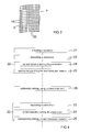
- Figure 4 shows a flow chart of the method step of providing a substrate 21, the cycles 22 of method steps including a method step of depositing 23 a passivation layer, a method step of etching 24 the passivation layer, which is preferably performed anisotropically, and a method step of etching 25 the semiconductor material, which is preferably performed isotropically. Between these cycles 22, the method step of applying 26 a different etchant is introduced.
- the DRIE process yields a through-substrate via having a comparatively smooth sidewall. The occurrence of leakage currents is thus avoided or at least drastically reduced.
- the described method can favourably be applied to produce any deep openings in a semiconductor body or substrate whenever relatively smooth vertical sidewalls are required.
- the method is facilitated by performing the additional etching in the equipment used for the etching and passivating cycles.
Landscapes
- Drying Of Semiconductors (AREA)
- Internal Circuitry In Semiconductor Integrated Circuit Devices (AREA)
Abstract
Description
- The invention relates to the field of semiconductor process technology and in particular to the production of through-substrate vias (TSVs) using DRIE (Deep Reactive Ion Etching). TSVs provide electric interconnections between opposite main sides of a semiconductor device and are useful for many applications, especially in three-dimensional integration of integrated circuits, for example.
-
WO 2012/031845 A1 discloses a manufacturing method for semiconductor devices comprising a through-substrate via. A contact hole is formed through the intermetal dielectric and the semiconductor material of the substrate, and a contact area of a metal plane that faces the substrate is exposed in the contact hole. A metallization is applied to form a contact on the contact area and an interconnection penetrating the substrate to contact an opposite further contact area facing away from the substrate. -
US 5,501,893 A discloses a method of anisotropically etching silicon to provide laterally defined recess structures. Silicon is removed by plasma etching using a reactive etching gas. A polymer former contained in the plasma is then used to generate a polymer layer on the etched surface, which inhibits the etching process until the polymer is removed. The etching step and the polymerizing step are alternatingly repeated. This method is generally known in the art as Bosch process, after the assignee of the patent, and is also known as pulsed or time-multiplexed etching. - In the Bosch process a standard, essentially isotropic plasma etching is performed to etch a deep opening in silicon. The plasma may comprise SF6, sulfur hexafluoride, for instance. After a few seconds of etching, a chemically inert passivation layer is formed to protect the silicon surface from further attack, thus inhibiting further etching. The passivation layer is typically formed from a polymer former contained in the plasma and may comprise C4F8, octafluorocyclobutane, for instance. In a subsequent anisotropic etching step, the passivation layer is removed from the bottom of the opening while remaining on the sidewall, so that only the bottom of the opening is subsequently again exposed to the etchant.
- The etching and polymerizing steps are alternatingly repeated, so that many small isotropic etching steps are performed, which yield an overall deep anisotropic etching. To etch through a 0.5 mm silicon wafer, for example, 100 to 1000 cycles of etching and polymerizing are performed. The sequence of polymer layers formed on the sidewall during consecutive etching and passivating cycles renders the sidewall undulated. When etching is completed, the sidewall of the opening comprises striations and a typical roughness. The cycle time can be adjusted: short cycles yield smoother walls, and long cycles yield a higher etch rate.
- It is an object of the present invention to disclose an improved method of producing an opening in a semiconductor substrate, especially a via hole for a TSV with reduced liability to electrical shorts or leakage currents.
- This object is achieved with the method of producing an opening in a semiconductor substrate according to
claim 1. Variants derive from the dependent claims. - The method of producing an opening in a semiconductor substrate comprises providing a substrate of semiconductor material having a main surface, forming an opening in the substrate from the main surface by deep reactive ion etching comprising a plurality of cycles, each of the cycles including a deposition of a passivation forming a passivation layer in the opening and an application of an etchant, and performing an additional etching between two consecutive cycles of the plurality of cycles by an application of a further etchant that is different from the etchant, whereby the passivation layer is etched on a sidewall of the opening.
- In a variant of the method, the passivation layer is removed from the sidewall of the opening.
- In further variants of the method, the additional etching is performed after at least one hundred or at least two hundred cycles of the plurality of cycles and before at least one hundred further cycles of the plurality of cycles.
- In a further variant of the method, the additional etching is performed after at least half (50%) of an intended depth of the opening has been etched.
- In a further variant of the method, the additional etching is performed after at least three fifths (60%) of the intended depth of the opening have been etched and before four fifths (80%) of the intended depth of the opening have been etched.
- In a further variant of the method, an oxygen plasma is employed in the additional etching.
- In a further variant of the method, the additional etching is isotropic.
- In further variants of the method, the additional etching is performed to have a duration that is at least three times or at least five times the duration of one of the cycles.
- In a further variant of the method, the passivation layer is formed by polymerization.
- In a further variant of the method, at least one further additional etching is performed between two further consecutive cycles of the plurality of cycles by a further application of the further etchant.
- In a further variant of the method, at least fifty cycles of the plurality of cycles are performed between the additional etching and the further additional etching.
- In a further variant of the method, a second further additional etching is performed. In particular, exactly three additional etching steps including an application of a further etchant may be performed during the entire etching process. The additional etching steps are separated from one another by an appropriate number of cycles of the plurality of cycles.
- In a further variant of the method, at least three hundred cycles are performed.
- In a further variant of the method, the opening is etched as a through-substrate via penetrating the substrate.
- In a further variant of the method, a metallization layer is arranged in the opening.
- The following is a detailed description of examples of the method.
- Figure 1
- is a cross section of a semiconductor substrate provided with an opening by DRIE.
- Figure 2
- is a cross section according to
Figure 1 after the formation of a through-substrate via. - Figure 3
- shows a section of a sidewall of the etched opening.
- Figure 4
- is a flow chart of the method.
- DRIE is liable to generate an ondulation on the sidewall of the etched opening as well as vertical striations and etching defects that may appropriately be designated as "pocketing". It has been found that such etching defects may cause electrical shorts or a rise in leakage currents occurring in a device comprising a through-substrate via formed by DRIE.
- The etching defects may build up from vertical striations during several cycles of etching and passivating, especially passivating by polymerization. When the striations reach a certain size, the deposition of polymer and hence the thickness of the passivation layer increase until the isotropic etching does no longer suffice to remove the added polymer. As a consequence, tile-shaped overhangs are formed, which shadow lateral portions of the striations from further deposition and thus generate an area of reduced resistance to the subsequent isotropic etching step. At a certain stage, a tiny pocket will be excavated at these locations, and a side track begins to form in the semiconductor material. The side track remains in the semiconductor material for the rest of the process and eventually forms a "pocketing" site.
- The method of producing an opening with smooth vertical sidewall in a semiconductor substrate aims at reducing the sidewall defects resulting from an anisotropic DRIE process. To this end, the sequence of cycles of etching and passivating is interrupted at least once, and an additional etching step with high selectivity to the semiconductor material, in particular silicon, is performed to remove at least a surface layer portion of the passivation layer from above the sidewall of the etched opening. After the additional etching, the main process is resumed with a succession of further cycles.
- The intermediate additional etching step may have a duration that is typically about five times as long as the duration of one of the regular cycles comprising etching and passivating. If the etching parameters are accordingly adjusted, it may suffice if the duration of the additional etching step is at least three times as long as the duration of one of the regular cycles of etching and passivating. The additional etching step is performed using a different etchant and may in particular employ an oxygen plasma, for example, with the process parameters set for an isotropic removal of at least a portion of the passivation layer, which may be a polymer, for instance.
- Semiconductor devices produced by the described method have been found to exhibit an improved yield of 97.8 %. A DRIE process using this method for the production of through-substrate vias having a depth of 200 µm and a width of 80 µm may typically comprise a total of 340 cycles. Every cycle consists of three consecutive steps: polymer deposition for 1.0 sec, anisotropic polymer etching for 1.1 sec, and isotropic silicon etching for 2.0 sec. The polymer forms a passivation layer. An intermediate isotropic polymer etching for about 15 sec may be performed immediately after the 200th cycle and the 290th cycle, for example. The impact of the additional etching steps is discernible in the roughness pattern of the sidewall.
-
Figure 1 is a cross section of asemiconductor substrate 1, which may be silicon, for instance. Thesubstrate 1 may be provided with anintegrated circuit 2 and a wiring comprising anintermetal dielectric 3, anupper passivation layer 4 andinterconnected wiring layers 5 embedded in theintermetal dielectric 3. A through-substate via may be provided to connect acontact area 6 of the wiring with an electric conductor arranged on the opposite side. Anopening 17 for the via is etched into thesubstrate 1 from amain surface 10 in the direction towards an opposite furthermain surface 11 of thesubstrate 1. Hence, in this example, the intended depth d of theopening 17 corresponds to a complete penetration of thesubstrate 1. Other depths d of theopening 17 may be suitable for other embodiments. In the embodiment shown inFigure 1 , the wiring is arranged above the furthermain surface 11, but the arrangement may be different. When theopening 17 uncovers thecontact area 6, a metallization can be applied to thecontact area 6 and thesidewall 7 of theopening 17 to form an electric interconnection through thesubstrate 1. - For the purpose of producing the
opening 17, plasma etching is performed to form a recess in thesubstrate 1. An etchant is used that is suitable to etch the semiconductor material. Sulfur hexafluoride can be used to etch silicon, for instance. Amask 8, which may be a structured resist, for instance, is applied at or above themain surface 10 and allows the etchant to attack the semiconductor material at the location where theopening 17 is to be formed. The etching may be essentially isotropic. InFigure 1 , the vertical etch attack, which increases the depth of the etched recess, is indicated by arrows as avertical direction 18. - In each cycle of the etching process, a thin passivation is formed, typically by polymerization generated by a polymer former provided in the plasma, for instance. The passivation interrupts the etching process until at least a
bottom layer 16 of the passivation has been removed by an essentially anisotropic etching. When the semiconductor material of thesubstrate 1 has been uncovered at the bottom of the recess orpartial opening 17, the etchant attacks the semiconductor material again, and the recess is etched deeper. - The
complete opening 17 is formed by reiterating the cycle of passivating and etching. In the course of repetition of the cycles, passivating bottom layers 16 are formed at decreasing distances from the furthermain surface 11 or from thecontact area 6, respectively, as indicated inFigure 1 with dotted contours. Apassivation layer 9 is eventually formed on theentire sidewall 7 of the etchedopening 17.Corrugations 19 formed on the surface of thepassivation layer 9 by the cycles of passivating and etching are schematically indicated inFigure 1 . The arrangement of thecorrugations 19 andvertical striations 20, which allow the etching defects to build up on thesidewall 7 of theopening 17, are schematically illustrated inFigure 3 . - The additional etching is performed to remove the described etching defects on the
sidewall 7 of theopening 17. Thereby thepassivation layer 9 is thinned and preferably removed from thesidewall 7. The effect of "pocketing" can thus be eliminated or at least reduced. -
Figure 2 shows a cross section according toFigure 1 after the formation of a through-substrate via by application of adielectric layer 12 on the bare semiconductor material of thesubstrate 1, ametallization layer 13 contacting thecontact area 6, afurther dielectric layer 14 on themetallization 13, and an optionalrear passivation layer 15, by way of example. Conductor tracks can be formed above themain surface 10 by themetallization layer 13 or by a structured further metallization. Thus the wiring can be connected with an electric terminal on the opposite side of the semiconductor device. -
Figure 4 shows a flow chart of the method step of providing asubstrate 21, thecycles 22 of method steps including a method step of depositing 23 a passivation layer, a method step of etching 24 the passivation layer, which is preferably performed anisotropically, and a method step of etching 25 the semiconductor material, which is preferably performed isotropically. Between thesecycles 22, the method step of applying 26 a different etchant is introduced. - Owing to one or several additional etching steps, the DRIE process yields a through-substrate via having a comparatively smooth sidewall. The occurrence of leakage currents is thus avoided or at least drastically reduced.
- Further to an opening intended for a through-substrate via, the described method can favourably be applied to produce any deep openings in a semiconductor body or substrate whenever relatively smooth vertical sidewalls are required. The method is facilitated by performing the additional etching in the equipment used for the etching and passivating cycles.
-
- 1
- substrate
- 2
- integrated circuit
- 3
- intermetal dielectric
- 4
- upper passivation layer
- 5
- wiring layer
- 6
- contact area
- 7
- sidewall
- 8
- mask
- 9
- passivation layer
- 10
- main surface
- 11
- further main surface
- 12
- dielectric layer
- 13
- metallization layer
- 14
- further dielectric layer
- 15
- rear passivation layer
- 16
- bottom layer
- 17
- opening
- 18
- vertical direction
- 19
- corrugation
- 20
- vertical striation
- 21
- method step of providing a substrate
- 22
- cycle of method steps
- 23
- method step of depositing a passivation layer
- 24
- method step of etching the passivation layer
- 25
- method step of etching the semiconductor material
- 26
- method step of applying a different etchant
Claims (14)
- A method of producing an opening in a semiconductor substrate, comprising:- providing (21) a substrate (1) of semiconductor material having a main surface (10), and- forming an opening (17) in the substrate (1) from the main surface (10) by deep reactive ion etching comprising a plurality of cycles (22), each of the cycles (22) including a deposition (23) of a passivation forming a passivation layer (9) in the opening (17) and an application (24, 25) of an etchant,characterized in that- an additional etching is performed between two consecutive cycles (22) of the plurality of cycles (22) by an application (26) of a further etchant that is different from the etchant, whereby the passivation layer (9) is etched on a sidewall (7) of the opening (17).
- The method of claim 1, wherein the passivation layer (9) is removed from the sidewall (7) of the opening (17).
- The method of claim 1 or 2, wherein the additional etching (26) is performed after at least half of an intended depth (d) of the opening (17) has been etched.
- The method of claim 3, wherein the additional etching (26) is performed after at least three fifths of the intended depth (d) of the opening (17) have been etched and before four fifths of the intended depth (d) have been etched.
- The method of one of claims 1 to 4, further comprising: an oxygen plasma being employed in the additional etching (26).
- The method of one of claims 1 to 5, wherein the additional etching (26) is isotropic.
- The method of one of claims 1 to 6, wherein the additional etching (26) is performed to have a duration that is at least three times a duration of one of the cycles (22).
- The method of claim 7, wherein the duration of the additional etching (26) is at least five times the duration of one of the cycles (22).
- The method of one of claims 1 to 8, further comprising: the passivation layer (9) being formed by polymerization.
- The method of one of claims 1 to 9, further comprising: at least one further additional etching being performed between two further consecutive cycles of the plurality of cycles (22) by a further application of the further etchant.
- The method of claim 10, wherein at least fifty cycles of the plurality of cycles (22) are performed between the additional etching (26) and the further additional etching.
- The method of one of claims 1 to 11, wherein a second further additional etching is performed.
- The method of one of claims 1 to 12, wherein the opening (17) is etched as a through-substrate via penetrating the substrate (1).
- The method of claim 13, further comprising:a metallization layer (13) being arranged in the opening (17).
Priority Applications (3)
| Application Number | Priority Date | Filing Date | Title |
|---|---|---|---|
| EP14189757.9A EP3012857A1 (en) | 2014-10-21 | 2014-10-21 | Method of producing an opening with smooth vertical sidewall in a semiconductor substrate |
| PCT/EP2015/073923 WO2016062614A1 (en) | 2014-10-21 | 2015-10-15 | Method of producing an opening with smooth vertical sidewall in a semiconductor substrate |
| US15/520,821 US10062610B2 (en) | 2014-10-21 | 2015-10-15 | Method of producing an opening with smooth vertical sidewall in a semiconductor substrate |
Applications Claiming Priority (1)
| Application Number | Priority Date | Filing Date | Title |
|---|---|---|---|
| EP14189757.9A EP3012857A1 (en) | 2014-10-21 | 2014-10-21 | Method of producing an opening with smooth vertical sidewall in a semiconductor substrate |
Publications (1)
| Publication Number | Publication Date |
|---|---|
| EP3012857A1 true EP3012857A1 (en) | 2016-04-27 |
Family
ID=51743373
Family Applications (1)
| Application Number | Title | Priority Date | Filing Date |
|---|---|---|---|
| EP14189757.9A Ceased EP3012857A1 (en) | 2014-10-21 | 2014-10-21 | Method of producing an opening with smooth vertical sidewall in a semiconductor substrate |
Country Status (3)
| Country | Link |
|---|---|
| US (1) | US10062610B2 (en) |
| EP (1) | EP3012857A1 (en) |
| WO (1) | WO2016062614A1 (en) |
Cited By (2)
| Publication number | Priority date | Publication date | Assignee | Title |
|---|---|---|---|---|
| TWI791531B (en) * | 2017-06-05 | 2023-02-11 | 英商Spts科技公司 | Methods of plasma etching and plasma dicing |
| CN121311043A (en) * | 2025-12-12 | 2026-01-09 | 上海邦芯半导体科技有限公司 | Methods for realizing glass through-hole structures and glass through-holes |
Families Citing this family (8)
| Publication number | Priority date | Publication date | Assignee | Title |
|---|---|---|---|---|
| US9971970B1 (en) * | 2015-04-27 | 2018-05-15 | Rigetti & Co, Inc. | Microwave integrated quantum circuits with VIAS and methods for making the same |
| US11121301B1 (en) | 2017-06-19 | 2021-09-14 | Rigetti & Co, Inc. | Microwave integrated quantum circuits with cap wafers and their methods of manufacture |
| US10529578B2 (en) * | 2017-11-12 | 2020-01-07 | Taiwan Semiconductor Manufacturing Co., Ltd. | Method of fabricating semiconductor structure |
| EP3490000B1 (en) * | 2017-11-24 | 2023-01-04 | ams AG | Near-infrared photodetector semiconductor device |
| US11262506B1 (en) * | 2020-08-07 | 2022-03-01 | Advanced Semiconductor Engineering, Inc. | Recessed portion in a substrate and method of forming the same |
| CN115084014B (en) * | 2022-06-29 | 2024-09-06 | 北京量子信息科学研究院 | Through-silicon via manufacturing method for superconducting quantum chip integrated circuit and integrated circuit |
| TW202614206A (en) * | 2024-06-07 | 2026-04-01 | 美商蘭姆研究公司 | Cyclic directional/isotropic etch |
| CN120280339B (en) * | 2025-06-10 | 2025-08-12 | 上海邦芯半导体科技有限公司 | Method for preparing semiconductor structure and semiconductor structure |
Citations (5)
| Publication number | Priority date | Publication date | Assignee | Title |
|---|---|---|---|---|
| US5501893A (en) | 1992-12-05 | 1996-03-26 | Robert Bosch Gmbh | Method of anisotropically etching silicon |
| US20080023846A1 (en) * | 2006-07-27 | 2008-01-31 | Sanyo Electric Co., Ltd. | Semiconductor device and manufacturing method of the same |
| EP2077577A1 (en) * | 2006-11-22 | 2009-07-08 | Sumitomo Precision Products Co., Ltd. | Silicon structure with opening having high aspect ratio, method for manufacturing the silicon structure, apparatus for manufacturing the silicon structure, program for manufacturing the silicon structure, and method for manufacturing etching mask for the silicon structure |
| US20090242512A1 (en) * | 2008-03-27 | 2009-10-01 | Dalsa Semiconductor Inc. | Deep reactive ion etching |
| WO2012031845A1 (en) | 2010-09-10 | 2012-03-15 | Austriamicrosystems Ag | Method for producing a semiconductor component with a through-contact and semiconductor component with through-contact |
Family Cites Families (1)
| Publication number | Priority date | Publication date | Assignee | Title |
|---|---|---|---|---|
| EP2741322B1 (en) * | 2012-12-10 | 2016-04-27 | ams AG | Semiconductor device with integrated hot plate and recessed substrate and method of production |
-
2014
- 2014-10-21 EP EP14189757.9A patent/EP3012857A1/en not_active Ceased
-
2015
- 2015-10-15 US US15/520,821 patent/US10062610B2/en active Active
- 2015-10-15 WO PCT/EP2015/073923 patent/WO2016062614A1/en not_active Ceased
Patent Citations (5)
| Publication number | Priority date | Publication date | Assignee | Title |
|---|---|---|---|---|
| US5501893A (en) | 1992-12-05 | 1996-03-26 | Robert Bosch Gmbh | Method of anisotropically etching silicon |
| US20080023846A1 (en) * | 2006-07-27 | 2008-01-31 | Sanyo Electric Co., Ltd. | Semiconductor device and manufacturing method of the same |
| EP2077577A1 (en) * | 2006-11-22 | 2009-07-08 | Sumitomo Precision Products Co., Ltd. | Silicon structure with opening having high aspect ratio, method for manufacturing the silicon structure, apparatus for manufacturing the silicon structure, program for manufacturing the silicon structure, and method for manufacturing etching mask for the silicon structure |
| US20090242512A1 (en) * | 2008-03-27 | 2009-10-01 | Dalsa Semiconductor Inc. | Deep reactive ion etching |
| WO2012031845A1 (en) | 2010-09-10 | 2012-03-15 | Austriamicrosystems Ag | Method for producing a semiconductor component with a through-contact and semiconductor component with through-contact |
Cited By (2)
| Publication number | Priority date | Publication date | Assignee | Title |
|---|---|---|---|---|
| TWI791531B (en) * | 2017-06-05 | 2023-02-11 | 英商Spts科技公司 | Methods of plasma etching and plasma dicing |
| CN121311043A (en) * | 2025-12-12 | 2026-01-09 | 上海邦芯半导体科技有限公司 | Methods for realizing glass through-hole structures and glass through-holes |
Also Published As
| Publication number | Publication date |
|---|---|
| WO2016062614A1 (en) | 2016-04-28 |
| US10062610B2 (en) | 2018-08-28 |
| US20170316976A1 (en) | 2017-11-02 |
Similar Documents
| Publication | Publication Date | Title |
|---|---|---|
| US10062610B2 (en) | Method of producing an opening with smooth vertical sidewall in a semiconductor substrate | |
| JP4518453B2 (en) | Silicon processing method using etching process | |
| US6712983B2 (en) | Method of etching a deep trench in a substrate and method of fabricating on-chip devices and micro-machined structures using the same | |
| US8951915B2 (en) | Methods for manufacturing a chip arrangement, methods for manufacturing a chip package, a chip package and chip arrangements | |
| JP5916105B2 (en) | Manufacturing method of semiconductor device | |
| KR20130031822A (en) | Method of forming and patterning conformal insulation layer in vias and etched structures | |
| CN109256334B (en) | Method for manufacturing laterally insulated integrated circuit chips | |
| US20130313718A1 (en) | Substrates Comprising Integrated Circuitry, Methods Of Processing A Substrate Comprising Integrated Circuitry, And Methods Of Back-Side Thinning A Substrate Comprising Integrated Circuitry | |
| TW201604993A (en) | Etching method of high aspect-ratio structure and manufacturing method of MEMS devices | |
| EP2693467B1 (en) | A method of producing a semiconductor device having an interconnect through the substrate | |
| US10529578B2 (en) | Method of fabricating semiconductor structure | |
| JP2016117155A (en) | Processing method of substrate and manufacturing method of liquid discharge head | |
| Ranganathan et al. | The development of a tapered silicon micro-micromachining process for 3D microsystems packaging | |
| US20150021745A1 (en) | Reactive ion etching | |
| Morgan et al. | Substrate interconnect technologies for 3-D MEMS packaging | |
| EP3312874A1 (en) | Method of forming a through-substrate via and a semiconductor device comprising a through-substrate via | |
| KR101541369B1 (en) | Improving Method of the Scallop's Characterization of Semiconductor Devices | |
| US12094717B2 (en) | Method for forming a trench in a first semiconductor layer of a multi-layer system | |
| JP5961794B2 (en) | Method for manufacturing silicon substrate having concavo-convex structure with high aspect ratio | |
| CN1891617A (en) | Method for protecting etched structure in induction coupling plasma etching | |
| EP1892757B1 (en) | High aspect ratio via etch | |
| US20130056858A1 (en) | Integrated circuit and method for fabricating the same | |
| DE102013206329B4 (en) | Method for realizing a vertical etch stop for a deep etching process and correspondingly prepared semiconductor substrate | |
| EP3358612A1 (en) | Method for selective etching using dry film photoresist | |
| KR100708941B1 (en) | Method for forming deep trenches of semiconductor devices |
Legal Events
| Date | Code | Title | Description |
|---|---|---|---|
| PUAI | Public reference made under article 153(3) epc to a published international application that has entered the european phase |
Free format text: ORIGINAL CODE: 0009012 |
|
| AK | Designated contracting states |
Kind code of ref document: A1 Designated state(s): AL AT BE BG CH CY CZ DE DK EE ES FI FR GB GR HR HU IE IS IT LI LT LU LV MC MK MT NL NO PL PT RO RS SE SI SK SM TR |
|
| AX | Request for extension of the european patent |
Extension state: BA ME |
|
| 17P | Request for examination filed |
Effective date: 20160908 |
|
| RBV | Designated contracting states (corrected) |
Designated state(s): AL AT BE BG CH CY CZ DE DK EE ES FI FR GB GR HR HU IE IS IT LI LT LU LV MC MK MT NL NO PL PT RO RS SE SI SK SM TR |
|
| RAP1 | Party data changed (applicant data changed or rights of an application transferred) |
Owner name: AMS AG |
|
| 17Q | First examination report despatched |
Effective date: 20200226 |
|
| STAA | Information on the status of an ep patent application or granted ep patent |
Free format text: STATUS: THE APPLICATION HAS BEEN REFUSED |
|
| 18R | Application refused |
Effective date: 20201231 |