EP3010149A2 - Resonant circuit with variable frequency and impedance - Google Patents
Resonant circuit with variable frequency and impedance Download PDFInfo
- Publication number
- EP3010149A2 EP3010149A2 EP15187022.7A EP15187022A EP3010149A2 EP 3010149 A2 EP3010149 A2 EP 3010149A2 EP 15187022 A EP15187022 A EP 15187022A EP 3010149 A2 EP3010149 A2 EP 3010149A2
- Authority
- EP
- European Patent Office
- Prior art keywords
- impedance
- resonators
- group
- matching element
- impedance matching
- Prior art date
- Legal status (The legal status is an assumption and is not a legal conclusion. Google has not performed a legal analysis and makes no representation as to the accuracy of the status listed.)
- Granted
Links
- 230000003068 static effect Effects 0.000 claims abstract description 25
- 230000006978 adaptation Effects 0.000 claims description 37
- 239000003990 capacitor Substances 0.000 claims description 30
- 239000000463 material Substances 0.000 claims description 23
- 239000000758 substrate Substances 0.000 claims description 11
- 230000000087 stabilizing effect Effects 0.000 claims description 2
- 230000004044 response Effects 0.000 description 21
- 239000010410 layer Substances 0.000 description 16
- 230000008878 coupling Effects 0.000 description 12
- 238000010168 coupling process Methods 0.000 description 12
- 238000005859 coupling reaction Methods 0.000 description 12
- 238000000034 method Methods 0.000 description 10
- 238000013459 approach Methods 0.000 description 9
- 239000011449 brick Substances 0.000 description 9
- 238000003780 insertion Methods 0.000 description 9
- 230000037431 insertion Effects 0.000 description 9
- XUIMIQQOPSSXEZ-UHFFFAOYSA-N Silicon Chemical compound [Si] XUIMIQQOPSSXEZ-UHFFFAOYSA-N 0.000 description 6
- 230000000694 effects Effects 0.000 description 6
- GQYHUHYESMUTHG-UHFFFAOYSA-N lithium niobate Chemical compound [Li+].[O-][Nb](=O)=O GQYHUHYESMUTHG-UHFFFAOYSA-N 0.000 description 6
- 230000005540 biological transmission Effects 0.000 description 5
- 238000005516 engineering process Methods 0.000 description 4
- 238000001914 filtration Methods 0.000 description 4
- 229910052710 silicon Inorganic materials 0.000 description 4
- 239000010703 silicon Substances 0.000 description 4
- 238000010897 surface acoustic wave method Methods 0.000 description 4
- RYGMFSIKBFXOCR-UHFFFAOYSA-N Copper Chemical compound [Cu] RYGMFSIKBFXOCR-UHFFFAOYSA-N 0.000 description 3
- 230000008859 change Effects 0.000 description 3
- 239000002131 composite material Substances 0.000 description 3
- 230000001276 controlling effect Effects 0.000 description 3
- 229910052802 copper Inorganic materials 0.000 description 3
- 239000010949 copper Substances 0.000 description 3
- 230000007423 decrease Effects 0.000 description 3
- 238000013461 design Methods 0.000 description 3
- 238000006073 displacement reaction Methods 0.000 description 3
- 230000005684 electric field Effects 0.000 description 3
- 230000003071 parasitic effect Effects 0.000 description 3
- 239000007787 solid Substances 0.000 description 3
- 230000015572 biosynthetic process Effects 0.000 description 2
- 210000004027 cell Anatomy 0.000 description 2
- 238000004891 communication Methods 0.000 description 2
- PMHQVHHXPFUNSP-UHFFFAOYSA-M copper(1+);methylsulfanylmethane;bromide Chemical compound Br[Cu].CSC PMHQVHHXPFUNSP-UHFFFAOYSA-M 0.000 description 2
- 230000000875 corresponding effect Effects 0.000 description 2
- 238000010586 diagram Methods 0.000 description 2
- 239000006185 dispersion Substances 0.000 description 2
- 238000010292 electrical insulation Methods 0.000 description 2
- 238000012423 maintenance Methods 0.000 description 2
- 238000004519 manufacturing process Methods 0.000 description 2
- 229910052751 metal Inorganic materials 0.000 description 2
- 239000002184 metal Substances 0.000 description 2
- 238000001465 metallisation Methods 0.000 description 2
- 238000002161 passivation Methods 0.000 description 2
- 230000001902 propagating effect Effects 0.000 description 2
- 239000002356 single layer Substances 0.000 description 2
- 238000001228 spectrum Methods 0.000 description 2
- 238000003786 synthesis reaction Methods 0.000 description 2
- 229910013641 LiNbO 3 Inorganic materials 0.000 description 1
- 229910002370 SrTiO3 Inorganic materials 0.000 description 1
- 241001080024 Telles Species 0.000 description 1
- 241000897276 Termes Species 0.000 description 1
- 238000009825 accumulation Methods 0.000 description 1
- 230000003466 anti-cipated effect Effects 0.000 description 1
- LFYJSSARVMHQJB-QIXNEVBVSA-N bakuchiol Chemical compound CC(C)=CCC[C@@](C)(C=C)\C=C\C1=CC=C(O)C=C1 LFYJSSARVMHQJB-QIXNEVBVSA-N 0.000 description 1
- 238000006243 chemical reaction Methods 0.000 description 1
- 150000001875 compounds Chemical class 0.000 description 1
- 230000006835 compression Effects 0.000 description 1
- 238000007906 compression Methods 0.000 description 1
- 230000002596 correlated effect Effects 0.000 description 1
- 230000001419 dependent effect Effects 0.000 description 1
- 239000003989 dielectric material Substances 0.000 description 1
- 230000005284 excitation Effects 0.000 description 1
- 230000001747 exhibiting effect Effects 0.000 description 1
- 238000002474 experimental method Methods 0.000 description 1
- 238000010438 heat treatment Methods 0.000 description 1
- 238000009413 insulation Methods 0.000 description 1
- 230000010354 integration Effects 0.000 description 1
- 239000000615 nonconductor Substances 0.000 description 1
- 238000005457 optimization Methods 0.000 description 1
- 230000008520 organization Effects 0.000 description 1
- UKDIAJWKFXFVFG-UHFFFAOYSA-N potassium;oxido(dioxo)niobium Chemical compound [K+].[O-][Nb](=O)=O UKDIAJWKFXFVFG-UHFFFAOYSA-N 0.000 description 1
- 230000035755 proliferation Effects 0.000 description 1
- 230000000717 retained effect Effects 0.000 description 1
- 238000004513 sizing Methods 0.000 description 1
- 239000003381 stabilizer Substances 0.000 description 1
- 238000012546 transfer Methods 0.000 description 1
- 238000013519 translation Methods 0.000 description 1
Images


Classifications
-
- H—ELECTRICITY
- H03—ELECTRONIC CIRCUITRY
- H03H—IMPEDANCE NETWORKS, e.g. RESONANT CIRCUITS; RESONATORS
- H03H3/00—Apparatus or processes specially adapted for the manufacture of impedance networks, resonating circuits, resonators
- H03H3/007—Apparatus or processes specially adapted for the manufacture of impedance networks, resonating circuits, resonators for the manufacture of electromechanical resonators or networks
- H03H3/02—Apparatus or processes specially adapted for the manufacture of impedance networks, resonating circuits, resonators for the manufacture of electromechanical resonators or networks for the manufacture of piezoelectric or electrostrictive resonators or networks
- H03H3/04—Apparatus or processes specially adapted for the manufacture of impedance networks, resonating circuits, resonators for the manufacture of electromechanical resonators or networks for the manufacture of piezoelectric or electrostrictive resonators or networks for obtaining desired frequency or temperature coefficient
-
- H—ELECTRICITY
- H03—ELECTRONIC CIRCUITRY
- H03H—IMPEDANCE NETWORKS, e.g. RESONANT CIRCUITS; RESONATORS
- H03H3/00—Apparatus or processes specially adapted for the manufacture of impedance networks, resonating circuits, resonators
- H03H3/007—Apparatus or processes specially adapted for the manufacture of impedance networks, resonating circuits, resonators for the manufacture of electromechanical resonators or networks
- H03H3/0072—Apparatus or processes specially adapted for the manufacture of impedance networks, resonating circuits, resonators for the manufacture of electromechanical resonators or networks of microelectro-mechanical resonators or networks
- H03H3/0073—Integration with other electronic structures
-
- H—ELECTRICITY
- H03—ELECTRONIC CIRCUITRY
- H03H—IMPEDANCE NETWORKS, e.g. RESONANT CIRCUITS; RESONATORS
- H03H3/00—Apparatus or processes specially adapted for the manufacture of impedance networks, resonating circuits, resonators
- H03H3/007—Apparatus or processes specially adapted for the manufacture of impedance networks, resonating circuits, resonators for the manufacture of electromechanical resonators or networks
- H03H3/0072—Apparatus or processes specially adapted for the manufacture of impedance networks, resonating circuits, resonators for the manufacture of electromechanical resonators or networks of microelectro-mechanical resonators or networks
- H03H3/0076—Apparatus or processes specially adapted for the manufacture of impedance networks, resonating circuits, resonators for the manufacture of electromechanical resonators or networks of microelectro-mechanical resonators or networks for obtaining desired frequency or temperature coefficients
-
- H—ELECTRICITY
- H03—ELECTRONIC CIRCUITRY
- H03H—IMPEDANCE NETWORKS, e.g. RESONANT CIRCUITS; RESONATORS
- H03H7/00—Multiple-port networks comprising only passive electrical elements as network components
- H03H7/38—Impedance-matching networks
-
- H—ELECTRICITY
- H03—ELECTRONIC CIRCUITRY
- H03H—IMPEDANCE NETWORKS, e.g. RESONANT CIRCUITS; RESONATORS
- H03H9/00—Networks comprising electromechanical or electro-acoustic devices; Electromechanical resonators
- H03H9/46—Filters
- H03H9/54—Filters comprising resonators of piezo-electric or electrostrictive material
- H03H9/542—Filters comprising resonators of piezo-electric or electrostrictive material including passive elements
-
- H—ELECTRICITY
- H03—ELECTRONIC CIRCUITRY
- H03H—IMPEDANCE NETWORKS, e.g. RESONANT CIRCUITS; RESONATORS
- H03H9/00—Networks comprising electromechanical or electro-acoustic devices; Electromechanical resonators
- H03H9/46—Filters
- H03H9/54—Filters comprising resonators of piezo-electric or electrostrictive material
- H03H9/545—Filters comprising resonators of piezo-electric or electrostrictive material including active elements
-
- H—ELECTRICITY
- H03—ELECTRONIC CIRCUITRY
- H03H—IMPEDANCE NETWORKS, e.g. RESONANT CIRCUITS; RESONATORS
- H03H9/00—Networks comprising electromechanical or electro-acoustic devices; Electromechanical resonators
- H03H9/46—Filters
- H03H9/54—Filters comprising resonators of piezo-electric or electrostrictive material
- H03H9/56—Monolithic crystal filters
- H03H9/566—Electric coupling means therefor
- H03H9/568—Electric coupling means therefor consisting of a ladder configuration
-
- H—ELECTRICITY
- H03—ELECTRONIC CIRCUITRY
- H03H—IMPEDANCE NETWORKS, e.g. RESONANT CIRCUITS; RESONATORS
- H03H9/00—Networks comprising electromechanical or electro-acoustic devices; Electromechanical resonators
- H03H9/46—Filters
- H03H9/64—Filters using surface acoustic waves
-
- H—ELECTRICITY
- H03—ELECTRONIC CIRCUITRY
- H03H—IMPEDANCE NETWORKS, e.g. RESONANT CIRCUITS; RESONATORS
- H03H9/00—Networks comprising electromechanical or electro-acoustic devices; Electromechanical resonators
- H03H9/70—Multiple-port networks for connecting several sources or loads, working on different frequencies or frequency bands, to a common load or source
- H03H9/703—Networks using bulk acoustic wave devices
- H03H9/706—Duplexers
-
- H—ELECTRICITY
- H03—ELECTRONIC CIRCUITRY
- H03H—IMPEDANCE NETWORKS, e.g. RESONANT CIRCUITS; RESONATORS
- H03H9/00—Networks comprising electromechanical or electro-acoustic devices; Electromechanical resonators
- H03H9/70—Multiple-port networks for connecting several sources or loads, working on different frequencies or frequency bands, to a common load or source
- H03H9/72—Networks using surface acoustic waves
- H03H9/725—Duplexers
-
- H—ELECTRICITY
- H03—ELECTRONIC CIRCUITRY
- H03H—IMPEDANCE NETWORKS, e.g. RESONANT CIRCUITS; RESONATORS
- H03H3/00—Apparatus or processes specially adapted for the manufacture of impedance networks, resonating circuits, resonators
- H03H3/007—Apparatus or processes specially adapted for the manufacture of impedance networks, resonating circuits, resonators for the manufacture of electromechanical resonators or networks
- H03H2003/0071—Apparatus or processes specially adapted for the manufacture of impedance networks, resonating circuits, resonators for the manufacture of electromechanical resonators or networks of bulk acoustic wave and surface acoustic wave elements in the same process
-
- H—ELECTRICITY
- H03—ELECTRONIC CIRCUITRY
- H03H—IMPEDANCE NETWORKS, e.g. RESONANT CIRCUITS; RESONATORS
- H03H3/00—Apparatus or processes specially adapted for the manufacture of impedance networks, resonating circuits, resonators
- H03H3/007—Apparatus or processes specially adapted for the manufacture of impedance networks, resonating circuits, resonators for the manufacture of electromechanical resonators or networks
- H03H3/02—Apparatus or processes specially adapted for the manufacture of impedance networks, resonating circuits, resonators for the manufacture of electromechanical resonators or networks for the manufacture of piezoelectric or electrostrictive resonators or networks
- H03H2003/027—Apparatus or processes specially adapted for the manufacture of impedance networks, resonating circuits, resonators for the manufacture of electromechanical resonators or networks for the manufacture of piezoelectric or electrostrictive resonators or networks the resonators or networks being of the microelectro-mechanical [MEMS] type
-
- H—ELECTRICITY
- H03—ELECTRONIC CIRCUITRY
- H03H—IMPEDANCE NETWORKS, e.g. RESONANT CIRCUITS; RESONATORS
- H03H3/00—Apparatus or processes specially adapted for the manufacture of impedance networks, resonating circuits, resonators
- H03H3/007—Apparatus or processes specially adapted for the manufacture of impedance networks, resonating circuits, resonators for the manufacture of electromechanical resonators or networks
- H03H3/02—Apparatus or processes specially adapted for the manufacture of impedance networks, resonating circuits, resonators for the manufacture of electromechanical resonators or networks for the manufacture of piezoelectric or electrostrictive resonators or networks
- H03H3/04—Apparatus or processes specially adapted for the manufacture of impedance networks, resonating circuits, resonators for the manufacture of electromechanical resonators or networks for the manufacture of piezoelectric or electrostrictive resonators or networks for obtaining desired frequency or temperature coefficient
- H03H2003/0414—Resonance frequency
- H03H2003/0464—Resonance frequency operating on an additional circuit element, e.g. a passive circuit element connected to the resonator
-
- H—ELECTRICITY
- H03—ELECTRONIC CIRCUITRY
- H03H—IMPEDANCE NETWORKS, e.g. RESONANT CIRCUITS; RESONATORS
- H03H3/00—Apparatus or processes specially adapted for the manufacture of impedance networks, resonating circuits, resonators
- H03H3/007—Apparatus or processes specially adapted for the manufacture of impedance networks, resonating circuits, resonators for the manufacture of electromechanical resonators or networks
- H03H3/02—Apparatus or processes specially adapted for the manufacture of impedance networks, resonating circuits, resonators for the manufacture of electromechanical resonators or networks for the manufacture of piezoelectric or electrostrictive resonators or networks
- H03H3/04—Apparatus or processes specially adapted for the manufacture of impedance networks, resonating circuits, resonators for the manufacture of electromechanical resonators or networks for the manufacture of piezoelectric or electrostrictive resonators or networks for obtaining desired frequency or temperature coefficient
- H03H2003/0414—Resonance frequency
- H03H2003/0471—Resonance frequency of a plurality of resonators at different frequencies
-
- H—ELECTRICITY
- H03—ELECTRONIC CIRCUITRY
- H03H—IMPEDANCE NETWORKS, e.g. RESONANT CIRCUITS; RESONATORS
- H03H3/00—Apparatus or processes specially adapted for the manufacture of impedance networks, resonating circuits, resonators
- H03H3/007—Apparatus or processes specially adapted for the manufacture of impedance networks, resonating circuits, resonators for the manufacture of electromechanical resonators or networks
- H03H3/02—Apparatus or processes specially adapted for the manufacture of impedance networks, resonating circuits, resonators for the manufacture of electromechanical resonators or networks for the manufacture of piezoelectric or electrostrictive resonators or networks
- H03H3/04—Apparatus or processes specially adapted for the manufacture of impedance networks, resonating circuits, resonators for the manufacture of electromechanical resonators or networks for the manufacture of piezoelectric or electrostrictive resonators or networks for obtaining desired frequency or temperature coefficient
- H03H2003/0414—Resonance frequency
- H03H2003/0478—Resonance frequency in a process for mass production
-
- H—ELECTRICITY
- H03—ELECTRONIC CIRCUITRY
- H03H—IMPEDANCE NETWORKS, e.g. RESONANT CIRCUITS; RESONATORS
- H03H9/00—Networks comprising electromechanical or electro-acoustic devices; Electromechanical resonators
- H03H9/02—Details
- H03H2009/02165—Tuning
-
- H—ELECTRICITY
- H03—ELECTRONIC CIRCUITRY
- H03H—IMPEDANCE NETWORKS, e.g. RESONANT CIRCUITS; RESONATORS
- H03H9/00—Networks comprising electromechanical or electro-acoustic devices; Electromechanical resonators
- H03H9/02—Details
- H03H2009/02165—Tuning
- H03H2009/02173—Tuning of film bulk acoustic resonators [FBAR]
- H03H2009/02188—Electrically tuning
- H03H2009/02196—Electrically tuning operating on the FBAR element, e.g. by direct application of a tuning DC voltage
-
- H—ELECTRICITY
- H03—ELECTRONIC CIRCUITRY
- H03H—IMPEDANCE NETWORKS, e.g. RESONANT CIRCUITS; RESONATORS
- H03H9/00—Networks comprising electromechanical or electro-acoustic devices; Electromechanical resonators
- H03H9/02—Details
- H03H2009/02165—Tuning
- H03H2009/02173—Tuning of film bulk acoustic resonators [FBAR]
- H03H2009/02188—Electrically tuning
- H03H2009/02204—Electrically tuning operating on an additional circuit element, e.g. applying a tuning DC voltage to a passive circuit element connected to the resonator
-
- H—ELECTRICITY
- H03—ELECTRONIC CIRCUITRY
- H03H—IMPEDANCE NETWORKS, e.g. RESONANT CIRCUITS; RESONATORS
- H03H9/00—Networks comprising electromechanical or electro-acoustic devices; Electromechanical resonators
- H03H9/02—Details
- H03H9/02244—Details of microelectro-mechanical resonators
- H03H2009/02488—Vibration modes
- H03H2009/02496—Horizontal, i.e. parallel to the substrate plane
-
- H—ELECTRICITY
- H03—ELECTRONIC CIRCUITRY
- H03H—IMPEDANCE NETWORKS, e.g. RESONANT CIRCUITS; RESONATORS
- H03H2210/00—Indexing scheme relating to details of tunable filters
- H03H2210/01—Tuned parameter of filter characteristics
- H03H2210/012—Centre frequency; Cut-off frequency
-
- H—ELECTRICITY
- H03—ELECTRONIC CIRCUITRY
- H03H—IMPEDANCE NETWORKS, e.g. RESONANT CIRCUITS; RESONATORS
- H03H2210/00—Indexing scheme relating to details of tunable filters
- H03H2210/02—Variable filter component
- H03H2210/021—Amplifier, e.g. transconductance amplifier
- H03H2210/023—Tuning of transconductance via tail current source
-
- H—ELECTRICITY
- H03—ELECTRONIC CIRCUITRY
- H03H—IMPEDANCE NETWORKS, e.g. RESONANT CIRCUITS; RESONATORS
- H03H2210/00—Indexing scheme relating to details of tunable filters
- H03H2210/03—Type of tuning
- H03H2210/033—Continuous
-
- H—ELECTRICITY
- H03—ELECTRONIC CIRCUITRY
- H03H—IMPEDANCE NETWORKS, e.g. RESONANT CIRCUITS; RESONATORS
- H03H9/00—Networks comprising electromechanical or electro-acoustic devices; Electromechanical resonators
- H03H9/46—Filters
- H03H9/64—Filters using surface acoustic waves
- H03H9/6403—Programmable filters
Definitions
- the field of the invention is that of resonant circuits and more particularly that of circuits that can be used in radio frequency filters whose central frequency and bandwidth are to be varied, in the context, for example, of telecommunications applications without thread.
- the transmitter / receiver of a multistandard system uses as many radio frequency filters or duplexers as the number of standards supported requires.
- Filters and duplexers have the property of selecting a fraction of the frequency spectrum - the so-called "useful" fraction of the system because it contains the information to be processed.
- the SAW / BAW filters exploit the electromechanical conversion of the energy contained in acoustic resonators, to perform a filtering function.
- the SAW resonator exploits acoustic vibrations confined to the surface of a piezoelectric substrate
- the BAW resonator is obtained by vibration in its thickness, a thin layer of piezoelectric material sandwiched between two electrodes.
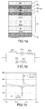
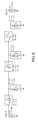
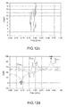
- FIGS. 1a, 1b and 1c illustrate the behavior of a BAW resonator.
- the figure 1a shows a conventional stack of materials for producing a "Solidly Mounted Resonator" type BAW resonator, comprising on the surface of a substrate S, a stack of layers Ci, providing a reflector function, and a layer of piezoelectric material Mpiézo between two electrodes Ei and Es, covered with a layer of dielectric l.
- the figure 1b shows the equivalent electrical scheme to the first order of a piezoelectric resonator and the figure 1c illustrates the resonance and antiresonance frequencies of the piezoelectric resonator.
- fs the resonance frequency
- fp the antiresonance frequency
- This parameter is directly related to the piezoelectric properties of the material and the vibration mode considered.
- the electromechanical coupling coefficient is of the order of 7%, and makes it possible to design filters with a bandwidth of order of 2%.
- a filter is obtained by the arrangement of several resonators, sometimes accompanied by additional passive elements.
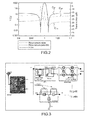
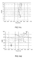
- resonators there are two types of resonators for designing a filter: the resonators placed in parallel with the signal path, and the resonators placed in series on the signal path. They are distinguished electrically by the frequency positioning of their resonance and antiresonance frequencies, arranged generally according to the diagram illustrated in FIG. figure 2 which gives the response of the filter (curve C 2F ).
- the resonant frequency of the resonators placed in series (curve C 2s ) is aligned with the antiresonance frequency of the resonators connected in parallel (curve C 2p ).
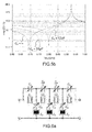
- the figure 3 presents the topology of a duplexer (association of two filters for the exchange of information in frequency duplex).
- a duplexer association of two filters for the exchange of information in frequency duplex.
- Another proposed solution consists in producing so-called composite resonators, based on the stacking of two piezoelectric layers.
- One of the layers is connected to the utilization circuit, while the other layer is connected to a tuning circuit, usually a variable capacitance for modifying the electrical boundary conditions that the volume acoustic wave sees in itself. propagating in the stack.
- This structure therefore makes it possible to present a resonator agile in frequency, and only controllable by a variable capacity, as described in the article of R.
- Aigner "Tunable acoustic RF-filters: Proceedings of the 40th European Microwave Conference, p. 787, 2010 .
- a capacitance in parallel with a resonator increases the static capacitance of the resonator, causing a displacement of the susceptance zero of the resonator (that is to say antiresonance) while leaving the pole unchanged (ie to say the resonance).
- the addition of a capacitance in series with a resonator decreases its characteristic impedance, and causes a displacement of the zero of reactance (that is to say the resonance) while leaving unchanged the pole (c that is, antiresonance). It is therefore possible to significantly shift the resonance and resonator frequencies of the resonator within the range delimited by the resonance and antiresonance frequencies of the original resonator, without the capacitive adjustment elements ( curve in solid lines).
- a very large electromechanical coupling coefficient becomes the necessary condition for a very high frequency agility.
- the filter of the figure 7a has a relative bandwidth of about 17%, based on the assumption of a piezoelectric material whose k 2 is 28%. It can be observed that according to the method indicated in figure 6a , the band of the filter is reduced on its lower edge while on its upper edge, the band is only slightly increased. In this case, we are working to reduce the bandwidth, essentially moving an edge. This therefore leads to also change the effective center frequency, with here a rate of the order of 3%.
- VSWR stationary wave ratio
- a stationary wave ratio generally satisfactory is 2, it corresponds to a reflection coefficient of -10 dB.
- Many systems tolerate a VSWR of 2.5, or -7.5 dB.
- the filters on the path of power transmission are very strict, and we seek a VSWR as low as possible (the theoretical minimum being 1). In the filters located at 0% and 11% of the figure 8 , the VSWR is well above 20.
- the points m7 and m9 are respectively relative to frequencies of 689 MHz and 923 MHz and have respective impedances of -6.5 dB and 90 dB.
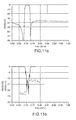
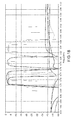
- FIGS. 15a, 15b , 15c and 15d are respectively related to insertion losses, adaptation, impedance (without serial capacitance and parallel capacitance) and impedance of resonant circuit couples (with varying series capacitance and parallel capacitance values) for a variable filter centered around 800MHz. It appears clearly in figure 15d , a problem of impedance variation for the different curves, relating to a frequency shift of about 60 MHz around the center frequency of 800 MHz.
- the constraint does not come from the working frequency, but from the frequency range that one seeks to cover, and the bandwidth of each filter that one seeks to achieve.
- the resonant circuits of the filter centered at 800MHz have a characteristic impedance of about 50 Ohms, while they vary at about 10 Ohms and about 200 Ohms, respectively at -60MHz and + 60MHz. This characteristic impedance dispersion is the main cause of the limitations of the approach.
- the Applicants propose a new solution making it possible to stabilize the characteristic impedance of a resonant circuit comprising a resonator at a chosen value and making it possible in particular to produce filters with an adjustable central frequency and an equally adjustable band. , while ensuring their impedance adaptation.
- the Applicants have explored a path against the state of the art and rather than vary the capabilities associated with a fixed resonator, the Applicants have studied the operation of a BAW filter constructed from a resonator (single layer) with variable surface area (and thus static capacity), and fixed associated capacitors, even if the variation of the static capacitance of a piezoelectric resonator is not a parameter that imposes itself directly. Indeed, the surface or the thickness of a resonator are fixed by the technology, it is about the physical dimensions of the component. This possibility is however available for the electrostrictive resonators mentioned in the prior art, although accompanied by other binding effects.
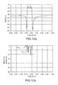
- the smallest “relaxed” resonator is at a lower frequency, while the larger “relaxed” resonator is at a higher frequency. It is observed that the response of the device is such that a filter of about 20 MHz (ie 2.5% of 800 MHz bandwidth) is obtained, and adapted from 725 MHz to 875 MHz, ie more than 18% around 800 MHz. . Moreover, the impedance plot of the series and parallel resonators show that they all have the same characteristic impedance, located around 50 Ohms. The figure 16d is remarkable proving this impedance stability.
- the filter thus produced therefore has the property of being at fixed bandwidth, and at variable central frequency.
- this new "variable impedance resonator" can also be associated with a variable reactive component in series and another in parallel. This association makes it possible to have a complete freedom on the frequency positioning of the resonance, the antiresonance, and the impedance of the whole. We thus obtain the possibility of making filters with variable bandwidth, and variable central frequency.
- the following table takes stock of all the surface values, serial capacitances and parallel capacities implemented within the topology represented in FIG. figure 17 , to perform the filtering functions illustrated in figure 18 , configured for TX bands 28, 17, 13 and 5.
- said set consisting of said group, said first impedance matching element and said second matching element has the impedance of a Butterworth-Van Dyke (BVD) model.
- VFD Butterworth-Van Dyke
- said group of N resonators consisting of several resonators Ri
- said first control means comprise a switching circuit for selecting and connecting one or more resonators.
- the resonators are volume wave resonators (BAW) which may have different geometric dimensions.
- BAW volume wave resonators
- the resonators are surface wave resonators (SAW), which may comprise different electrode arrangements on the surface of a piezoelectric substrate.
- SAW surface wave resonators
- said resonator has a variable capacitance whose value is a function of the value of an electrical control signal, said first means comprising means for varying said electrical signal control.
- Said resonator may be an electrostrictive resonator based on BST material.
- At least one impedance matching element is a capacitor, an inductor or a set of passive elements.
- At least one impedance matching element is an active circuit that may comprise transistors.
- the second impedance matching element is connected on the one hand to one of the input / output terminals and on the other hand to an intermediate node between the resonator group and said first element impedance matching.
- the second impedance matching element is placed between the input and output terminals, connected in parallel with the set: set of resonators / impedance matching element placed serial.
- the first chip further comprises the first and second impedance matching elements.
- the second chip further comprises the first and second impedance matching elements.
- the invention also relates to a filter comprising a set of resonant circuits according to the invention.
- the invention also relates to a duplexer comprising a set of resonant circuits according to the invention.
- the first and second control means for varying respectively the characteristic impedance Zc of said first group, the impedances of the first and second impedance matching elements are typically selective addressing means that can typically be switches with controls. associated.
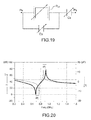
- the figure 19 illustrates a first variant of the resonant circuit of the invention, the non-zero reactance elements being capacitors.
- This figure highlights between a terminal or an input port Pe and a terminal or an output port Ps, the group schematized by a resonator R C0 with a static capacitance C 0 variable, associated with the first impedance matching element nonzero reactance represented by a variable capacitance in series Cs and associated with the second nonzero reactance impedance matching element represented by a variable capacitance in parallel Cp, the arrows indicating a command making it possible to vary in particular the values of impedance.
- variable capacitors can also be replaced by variable inductances in series and in parallel, or else by a combination of inductances and capacitors in series and in parallel.
- the properties of the set are then substantially different, and potentially open to new applications of the invention.
- the invention indeed assumes the combination of variable reactive elements of any kind, with a group of resonators constituting a characteristic variable impedance resonator.
- the impedance Z of a resonator is characterized in the first approach by the impedance of its equivalent model of Butterworth-Van Dyke (BVD), previously presented and illustrated in FIG. figure 1 , irrespective of any losses:
- the m VS m ⁇ 2 - 1 NOT D
- the figure 20 highlights the frequency response of the impedance Z and that Z as well as C 0 .
- This feature is a fundamental feature of the present invention.
- the figure 21 illustrates a second variant of the invention in which the capacitor Cp, mounted in parallel, is mounted differently from that of the previous variant. It is placed in parallel with the assembly consisting of the resonator and the series element Cs.
- a first technique consists in varying the geometrical dimensions of the resonator. If there are techniques in the field of microwave cavity filters for modifying the physical dimensions of the resonators by mechanical means (servomotors or simply adjustment screws), such means are not conceivable in the case of integrated resonators.
- a single "large" resonator R C0 variable static capacity C 0 may be equivalent to a group of elementary resonators Ri arranged in parallel, the different resonators having identical resonance and antiresonance frequencies, but whose static capacity is such that the sum of the basic static capacities is equal to the static capacity C 0 .
- FIG 23 Such a configuration is illustrated in figure 23 and shows this first embodiment including switches and associated controls, for switching elementary resonators and unitary reactive components.
- BAW resonators with a wide range of variation can be designed from LNO material, according to a known manufacturing process and described in the article by Pijolat, M. Deguet, C. Billard, C. Mercier, D. , Reinhardt, A., "Bias controlled electrostrictive longitudinal resonance in X-cut lithium niobate thin resonator films ,” Applied Physics Letters, Volume: 98, Issue: 23.
- the switches can be designed from transistors, the dimensioning of which involves a compromise between their internal parasitic resistance during the "closed” state, and their internal parasitic capacitance during the "open” state.
- Elementary capacitors for their part, are conventionally made by placing a thin dielectric layer sandwiched between two metal electrodes. The quality of the dielectric material and the electrodes intervenes in the operation of the assembly.
- the figure 24 illustrates in more detail an example of interconnections of the two chips in the context of a first chip in LNO and a second chip HR-SOI (integrated circuit manufacturing technology using a thin layer of silicon High Resistivity (HR) arranged on a layer of electrical insulation, itself covering a solid substrate of silicon).
- HR-SOI integrated circuit manufacturing technology using a thin layer of silicon High Resistivity (HR) arranged on a layer of electrical insulation, itself covering a solid substrate of silicon).
- the Pu 10 and Pu 20 chips are interconnected via Pu10-Pu20 abutments comprising an intermediate metallization portion 300 and a contact metallization portion 301.
- the resonant circuit comprises acoustic surface wave resonators.
- These resonators are advantageously produced on highly piezoelectric substrates such as lithium niobate having a crystalline orientation allowing the excitation of strongly coupled surface waves, for example of the "pseudo-surface wave" type.
- the characteristic impedance no longer depends on the surface of a planar capacitor, but on a capacitance produced by the arrangement of interdigitated electrodes.
- a SAW resonator with 10 N electrodes can be obtained by placing 10 SAW resonators with N electrodes each in parallel. Setting at the level of the controls and interconnections may be equivalent to that described in the context of the first embodiment.
- the resonators are electrostrictive resonators, that is to say to the piezoelectric properties activatable under the effect of a voltage.
- This is the case, for example, with BST material, a crystallographic organization material called perovskite. This material was used in the context of the patent application EP2405574 .
- the antiresonance frequency (Fp) decreases slightly (1.5%) when the applied voltage increases (up to 10 V), while the resonance frequency (Fs) decreases by 5% over the same voltage range.
- the characteristic impedance remains at 50 ⁇ +/- 10 ⁇ . This type of variation does not allow the realization of the solution of the present the two remarkable frequencies as well as the characteristic impedance evolve interdependently.
- Such a chip is then connected to an active circuit responsible for providing a bias voltage for each resonator and capacitor, so as to dynamically adjust the values of the static capacitances of the resonators, and the capacitors added to the resonators.
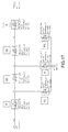
- the figure 27 schematizes this third example of circuit according to the invention, in which two chips are interconnected.
- One chip integrates the functions of resonators R C0 and the capacitors Cp and Cs
- another chip integrates the control means of the ferroelectric capacitors and those of the electrostrictive resonators.
- the first chip Pu 11 comprises the control means 14 of the electrostrictive resonator and the control means 15, 16 of the ferroelectric capacitors.
- the second chip Pu 21 comprises the electrostrictive resonator R C0 and the ferroelectric capacitors Cp and Cs.
- the reactive components are made with active circuits.
Abstract
L'invention a pour objet un circuit résonant comprenant une borne d'entrée (Pe) et une borne de sortie (Ps) et au moins : - un groupe de N résonateurs avec N ¥1, ayant la même fréquence de résonance et la même fréquence d'antirésonance ; - un premier et un second éléments d'adaptation d'impédance (Cs, Cp) présentant une réactance non nulle, le premier élément étant en série avec ledit groupe de résonateurs, et le second élément étant en parallèle avec ledit groupe de résonateurs ledit circuit résonant comprenant : - des premiers moyens de commande dudit groupe de résonateurs permettant de fixer la capacité statique (C 0 ) dudit groupe à une première valeur ; - des second moyens de commande permettant de fixer l'impédance du premier élément et celle du second élément à des secondes valeurs ; lesdites première et secondes valeurs étant telles que : le triplet de valeurs : capacité statique dudit groupe / impédance du premier élément/ impédance du second élément (C 0 , Cs, Cp) permet de déterminer le triplet de paramètres suivants : o l'impédance caractéristique Z c de l'ensemble constitué par ledit groupe, ledit premier élément d'adaptation d'impédance et ledit second élément d'adaptation ; o la fréquence de résonance É r dudit ensemble; o la fréquence d'antirésonance É a dudit ensemble, pour stabiliser l'impédance dudit circuit à une impédance caractéristique choisie.The subject of the invention is a resonant circuit comprising an input terminal (Pe) and an output terminal (Ps) and at least: - a group of N resonators with N ‰¥1, having the same resonance frequency and the same antiresonance frequency; - a first and a second impedance matching element (Cs, Cp) having a non-zero reactance, the first element being in series with the said group of resonators, and the second element being in parallel with the said group of resonators said resonant circuit comprising: - first control means of said group of resonators making it possible to fix the static capacitance (C 0 ) of said group at a first value; - second control means making it possible to fix the impedance of the first element and that of the second element at second values; said first and second values being such that: the triplet of values: static capacitance of said group/impedance of the first element/impedance of the second element (C 0 , Cs, Cp) makes it possible to determine the following triplet of parameters: o the characteristic impedance Z c of the assembly formed by said group, said first impedance matching element and said second matching element; o the resonant frequency É r of said set; o the antiresonance frequency É a of said set, to stabilize the impedance of said circuit to a selected characteristic impedance.
Description
Le domaine de l'invention est celui des circuits résonants et plus particulièrement celui des circuits pouvant être utilisés dans des filtres radiofréquences dont on cherche à faire varier la fréquence centrale et la largeur de bande, dans le cadre par exemple d'applications de télécommunications sans fil.The field of the invention is that of resonant circuits and more particularly that of circuits that can be used in radio frequency filters whose central frequency and bandwidth are to be varied, in the context, for example, of telecommunications applications without thread.
Les architectures actuelles de systèmes de télécommunication sont conçues de telle manière qu'elles peuvent s'adapter à plusieurs standards de communication. On dit qu'elles sont multistandards. C'est là une propriété essentielle qui permet à un système de fonctionner dans plusieurs régions géographiques et avec l'aide de plusieurs réseaux. Pour réaliser cette fonction, les systèmes actuels reposent en réalité sur une batterie de sous-systèmes mis en parallèle, et commutés en fonction du scénario d'utilisation.Current architectures of telecommunication systems are designed in such a way that they can adapt to several communication standards. They are said to be multistandard. This is an essential property that allows a system to operate in multiple geographic areas and with the help of multiple networks. To achieve this function, the current systems are actually based on a battery of subsystems that are paralleled and switched according to the usage scenario.
En particulier, l'émetteur/récepteur d'un système multistandard exploite autant de filtres radiofréquences ou duplexeurs que le nombre de standards pris en charge l'exige. Les filtres et les duplexeurs ont la propriété de sélectionner une fraction du spectre fréquentiel - la fraction dite « utile » au système, parce qu'elle contient l'information à traiter.In particular, the transmitter / receiver of a multistandard system uses as many radio frequency filters or duplexers as the number of standards supported requires. Filters and duplexers have the property of selecting a fraction of the frequency spectrum - the so-called "useful" fraction of the system because it contains the information to be processed.
Aujourd'hui, ces filtres sont majoritairement réalisés à l'aide de la technologie piézoélectrique, et ils se déclinent en deux grandes familles : les filtres utilisant des résonateurs à ondes de surface « Surface Acoustic Wave » ou « SAW » et les filtres utilisant des résonateurs à ondes de volume « Bulk Acoustic Wave » ou « BAW ». Ce type de filtres s'est imposé dans les systèmes de télécommunications parce qu'ils sont aujourd'hui relativement simples à réaliser de manière intégrée, et occupent donc un espace minimum (quelques millimètres carrés) pour un coût économiquement satisfaisant.Today, these filters are mostly made using piezoelectric technology, and they fall into two main families: filters using surface acoustic wave resonators "Surface Acoustic Wave" or "SAW" and filters using bulk wave resonators "Bulk Acoustic Wave" or "BAW". This type of filter has become essential in telecommunications systems because they are today relatively simple to achieve in an integrated manner, and therefore occupy a minimum space (a few square millimeters) for an economically satisfactory cost.
Cependant, ces composants fonctionnent avec l'aide d'un matériau et d'une architecture qui imposent une fréquence centrale et une largeur de bande pour chacun.However, these components work with the help of a material and architecture that impose a center frequency and a bandwidth for each.
Or, avec la multiplication des standards de télécommunications, et les spécificités géographiques, le nombre de ces composants de filtrage dans les systèmes embarqués a tendance à augmenter. Il devient désormais très utile de trouver un moyen de rendre les filtres variables en fréquence centrale et en largeur de bande, de manière à réduire leur nombre, voire à n'en avoir plus qu'un seul.However, with the proliferation of telecommunications standards, and geographic specificities, the number of these filtering components in embedded systems tends to increase. It now becomes very useful to find a way to make the variable filters in center frequency and in bandwidth, so as to reduce their number, or even to have only one.
De manière générale construits autour d'un matériau aux propriétés piézoélectriques, les filtres SAW/BAW exploitent la conversion électromécanique de l'énergie contenue dans des résonateurs acoustiques, pour réaliser une fonction de filtrage.In general, built around a material with piezoelectric properties, the SAW / BAW filters exploit the electromechanical conversion of the energy contained in acoustic resonators, to perform a filtering function.
Alors que le résonateur SAW exploite des vibrations acoustiques confinées à la surface d'un substrat piézoélectrique, le résonateur BAW est obtenu par vibration dans son épaisseur, d'une mince couche de matériau piézoélectrique prise en sandwich entre deux électrodes.While the SAW resonator exploits acoustic vibrations confined to the surface of a piezoelectric substrate, the BAW resonator is obtained by vibration in its thickness, a thin layer of piezoelectric material sandwiched between two electrodes.
Les
Plus précisément, la
Dans les deux cas SAW/BAW, ce phénomène acoustique s'interprète sur le plan électrique comme l'agencement d'un résonateur « RLC » en parallèle avec une capacité. Ce modèle, très répandu dans la littérature, est communément désigné par l'abréviation « BVD », pour « Butterworth-Van Dyke ». Il présente alors une résonance série (quasi-court-circuit) et une antirésonance (quasi-circuit-ouvert). La distance fréquentielle qui sépare la résonance de l'antirésonance est caractérisée par le coefficient de couplage électromécanique du résonateur défini par l'équation suivante : 
avec fs : la fréquence de résonance et fp : la fréquence d'antirésonance.with fs: the resonance frequency and fp: the antiresonance frequency.
Ce paramètre est directement lié aux propriétés piézoélectriques du matériau et au mode de vibration considéré.This parameter is directly related to the piezoelectric properties of the material and the vibration mode considered.
Typiquement, pour des ondes de volume se propageant dans de l'AIN (Nitrure d'Aluminium), le coefficient de couplage électromécanique est de l'ordre de 7%, et permet de concevoir des filtres dont la largeur de bande est de l'ordre de 2%.Typically, for volume waves propagating in AIN (Aluminum Nitride), the electromechanical coupling coefficient is of the order of 7%, and makes it possible to design filters with a bandwidth of order of 2%.
Un filtre est obtenu par l'agencement de plusieurs résonateurs, parfois accompagnés d'éléments passifs supplémentaires. Typiquement, on distingue deux genres de résonateurs pour concevoir un filtre : les résonateurs mis en parallèle au chemin du signal, et les résonateurs mis en série sur le chemin du signal. Ils se distinguent électriquement par le positionnement fréquentiel de leurs fréquences de résonance et d'antirésonance, disposées généralement selon le schéma illustré en
En particulier, la fréquence de résonance des résonateurs mis en série (courbe C2s), est alignée sur la fréquence d'antirésonance des résonateurs mis en parallèle (courbe C2p).In particular, the resonant frequency of the resonators placed in series (curve C 2s ) is aligned with the antiresonance frequency of the resonators connected in parallel (curve C 2p ).
Les résonateurs acoustiques, en dehors de leurs fréquences remarquables, présentent un comportement capacitif, et présentent donc une impédance qui dépend en premier lieu de leur capacité statique équivalente. On nomme plus tard « impédance caractéristique Zc » cette impédance liée au comportement capacitif d'un résonateur en dehors de ses fréquences remarquables. Le dimensionnement de ce condensateur intervient dans l'adaptation d'impédance du filtre. On montre que lorsque les résonateurs séries et parallèles sont disposés selon le principe décrit ci-avant, l'adaptation du filtre est obtenue si l'impédance Zeq du générateur et de la charge équivaut à la moyenne géométrique des impédances caractéristiques des résonateurs : 
Pour exemple, la
Tandis que l'agencement des résonateurs sur le chemin « RX » est différentiel et croisé (dit « Treillis », ou lattice en anglais), les résonateurs sur le chemin TX sont disposés en « échelle » (Ladder en anglais).While the arrangement of the resonators on the path "RX" is differential and crossed (called " lattice " or lattice in English), the resonators on the TX path are arranged in "ladder" ( Ladder in English).
A ce jour, quelques industriels dominent le marché des filtres/duplexeurs à base de BAW ou de SAW. Tous sans exception proposent des batteries de composants, chaque composant adressant une bande fréquentielle spécifique, ou un standard spécifique (dans le cas des duplexeurs). Ceci est imposé par les propriétés intrinsèques du matériau piézoélectrique, ainsi que par l'approche architecturale des filtres, comme explicité ci-après dans la présente description.To date, some manufacturers dominate the market of filters / duplexers based on BAW or SAW. All without exception offer component batteries, each component addressing a specific frequency band, or a specific standard (in the case of duplexers). This is imposed by the intrinsic properties of the piezoelectric material, as well as by the architectural approach of the filters, as explained hereinafter in the present description.
Dès 2005 a été publiée une proposition visant à modifier les fréquences remarquables des résonateurs acoustiques, ouvrant ainsi la voie aux filtres variables comme décrit dans l'article de
Cependant en 2006 et 2007, cette même équipe démontre qu'avec l'aide d'un circuit actif, il est possible de modifier la fréquence centrale d'un filtre de 0.3%. Ils en concluent que la méthode peut rattraper des dispersions technologiques. Il est possible de présumer que cette méthode a peu de chance de conduire à une véritable agilité du filtre, comme décrit dans l'article de :
A partir des conclusions de cette étude, la plupart des équipes travaillant sur ce sujet ont cherché des solutions permettant de se passer d'éléments passifs ajoutés à des résonateurs, en se concentrant sur des moyens de modifier la vitesse de propagation des ondes acoustiques.From the conclusions of this study, most of the teams working on this topic have sought solutions to do without passive elements added to resonators, focusing on ways to change the speed of propagation of acoustic waves.
C'est ainsi que des résonateurs reposant sur l'usage de matériaux électrostrictifs ont été proposés, comme décrit dans l'article de
Une autre solution proposée consiste à réaliser des résonateurs dits composites, reposant sur l'empilement de deux couches piézoélectriques. L'une des couches est connectée au circuit d'utilisation, tandis que l'autre couche est connectée à un circuit d'accord, habituellement une capacité variable permettant de modifier les conditions aux limites électriques que voit l'onde acoustique de volume en se propageant dans l'empilement. Cette structure permet donc de présenter un résonateur agile en fréquence, et uniquement pilotable par une capacité variable, comme décrit dans l'article de
L'approche la plus prometteuse est celle suivie depuis quelques années par une équipe japonaise dirigée par Ken-Ya Hashimoto de l'université de Chiba, abondamment décrite dans les articles suivants :
Cette équipe s'emploie à démontrer que la première approche mentionnée ci-dessus est en réalité envisageable, dès lors que l'on dispose de résonateurs réalisés avec des matériaux à très grand coefficient de couplage électromécanique. En effet, l'ajout d'éléments passifs variables en série ou en parallèle à un résonateur acoustique permet de déplacer les fréquences de résonance et d'antirésonance comme illustré sur les
Pour exploiter ce principe, on découvre dès 2010 les topologies illustrées en
Selon que l'on associe des résonateurs et des capacités, conformément à la topologie de la
Le filtre de la
Dans le cas de la
Cependant cette solution comporte une forte limite d'exploitation. En effet, les auteurs de l'étude réalisent deux filtres de 5 % de bande, centrés à 4 % et à 9 % de la fréquence de résonance des résonateurs en série. En d'autres termes, ils ne cherchent pas à couvrir l'ensemble du spectre que l'on pourrait supposer exploitable compte tenu du coefficient de couplage de 30 %. Une étude plus poussée de ces travaux montre en effet que très vite, les valeurs des capacités associées sont telles que l'impédance caractéristique du filtre varie de manière si prononcée que son adaptation n'est plus assurée. C'est ce que l'on observe sur la
Le déplacement des résonances et antirésonances sur une large plage de variation (à l'extrême, sur toute la plage autorisée par le coefficient de couplage) suppose l'usage de capacités variables dont les valeurs sont, ou bien très grandes, ou bien très petites devant la capacité naturelle des résonateurs. Dès lors, les conditions d'adaptation ne sont plus observées, et les pertes d'insertion du filtre augmentent. C'est notamment ce que l'on peut observer sur les courbes centrées à 0 % et à 11 %.The displacement of the resonances and antiresonances over a wide range of variation (at the extreme, over the whole range allowed by the coupling coefficient) assumes the use of variable capacities whose values are either very large or very small. in front of the natural capacity of the resonators. As a result, the adaptation conditions are no longer observed, and the insertion losses of the filter increase. This is what can be observed on curves centered at 0% and at 11%.
La désadaptation provoque également un taux d'onde stationnaire (VSWR) aux entrées/sorties du filtre. Un taux d'onde stationnaire généralement satisfaisant vaut 2, il correspond à un coefficient de réflexion de -10 dB. Beaucoup de systèmes tolèrent un VSWR de 2.5, soit -7.5 dB. Mais les filtres situés sur le chemin de la transmission en puissance sont très stricts, et l'on cherche un VSWR le plus faible possible (le minimum théorique étant 1). Dans les filtres situés à 0 % et 11 % de la
Dans ce contexte et pour mieux appréhender la problématique, les Demandeurs ont étudié plus précisément l'exemple de configuration illustrée en
A partir de cette architecture, les Demandeurs ont cherché à adresser plusieurs bandes de fréquences : les bandes TX numérotés 28, 17, 13, 8 et 5 du protocole LTE, ces bandes étant respectivement présentées sur les
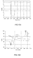
- les
figures 10a ,11a ,12a ,13a et14a sont relatives à la réponse en transmission du filtre (S21 ou S12) ; - les
figures 10b ,11 b ,12b ,13b et14b sont relatives à la réponse en réflexion du filtre (S11 ou S22), plus précisément :- ∘ les courbes C10b1, C11b1, C12b1, C13b1 et C14b1 sont relatives à la réponse S(4,4) en réflexion exprimée en dB du filtre illustré en
figure 9 ; - ∘ les courbes C10b2, C11b2, C12b2, C13b2 et C14b2 sont relatives à la réponse S(5,5) en réflexion du filtre exprimée en dB illustré en
figure 9 ;
- ∘ les courbes C10b1, C11b1, C12b1, C13b1 et C14b1 sont relatives à la réponse S(4,4) en réflexion exprimée en dB du filtre illustré en
- les
figures 10c ,11 c ,12c ,13c et14c sont relatives au taux d'onde stationnaire (VSWR), calculé au port Num4 ; - les
figures 10d ,11d ,12d ,13d et14d montrent :- ∘ les courbes C10d1, C 11d1, C 12d1, C 13d1 et C 14d1 relatives à l'impédance du résonateur dit « relaxé », c'est-à-dire sans aucune capacité variable, fixée par ses dimensions et les caractéristiques technologiques de la couche piézoélectrique ;
- ∘ les courbes C10d2, C 11d2, C 12d2, C 13d2 et C 14d2 relatives à la réponse en impédance de la brique parallèle, constituée du résonateur « relaxé » et des capacités associées ;
- ∘ les courbes C10d3, C 11d3, C 12d3, C 13d3 et C 14d3 relatives à la réponse de la brique série, constituée d'un résonateur identique à la brique parallèle, et de capacités associées différentes de celles de la brique parallèle.
- the
figures 10a ,11a ,12a ,13a and14a are related to the transmission response of the filter (S 21 or S 12 ); - the
figures 10b ,11 b ,12b ,13b and14b are relative to the reflection response of the filter (S 11 or S 22 ), more precisely:- ∘ curves C 10b1 , C 11b1 , C 12b1 , C 13b1 and C 14b1 relate to the S (4.4) reflection response expressed in dB of the filter illustrated in FIG.
figure 9 ; - ∘ the curves C 10b2 , C 11b2 , C 12b2 , C 13b2 and C 14b2 relate to the response S (5.5) in reflection of the filter expressed in dB illustrated in FIG.
figure 9 ;
- ∘ curves C 10b1 , C 11b1 , C 12b1 , C 13b1 and C 14b1 relate to the S (4.4) reflection response expressed in dB of the filter illustrated in FIG.
- the
Figures 10c ,11 c ,12c ,13c and14c are relative to the stationary wave ratio (VSWR), calculated at port Num4; - the
figures 10d ,11d ,12d ,13d and14d show:- ∘ curves C 10d1 , C 11d1 , C 12d1 , C 13d1 and C 14d1 relating to the impedance of the resonator said "relaxed", that is to say without any variable capacity, fixed by its dimensions and the technological features of the piezoelectric layer;
- ∘ curves C 10d2 , C 11d2 , C 12d2 , C 13d2 and C 14d2 relating to the impedance response of the parallel brick, consisting of the "relaxed" resonator and associated capacitances;
- ∘ curves C 10d3 , C 11d3 , C 12d3 , C 13d3 and C 14d3 relating to the response of the series brick, consisting of a resonator identical to the parallel brick, and associated capacities different from those of the parallel brick.
Les points m7 et m9 sont respectivement relatifs à des fréquences de 689MHz et 923MHz et présentent des impédances respectives de -6,5 dB et 90 dB.The points m7 and m9 are respectively relative to frequencies of 689 MHz and 923 MHz and have respective impedances of -6.5 dB and 90 dB.
On constate, comme anticipé par l'état de l'art antérieur, que lorsqu'on définit un résonateur optimal pour la bande 28, il est possible de parvenir par exemple à réaliser la bande 17 (734-746 MHz), tandis que les autres bandes ne peuvent être réalisées dans des conditions correctes, c'est-à-dire avec un taux d'onde stationnaire de l'ordre de 2.It can be seen, as anticipated by the state of the prior art, that when defining an optimum resonator for the band 28, it is possible to achieve, for example, the band 17 (734-746 MHz), while the other bands can not be performed under correct conditions, that is to say with a stationary wave ratio of the order of 2.
Les Demandeurs ont également mené l'étude en choisissant un résonateur optimal pour le centre de la plage de variation, c'est-à-dire centré sur 800 MHz (permettant un fonctionnement optimal en bande 13 et trois fois plus gros que celui calibré pour la bande 28) : on parvient à la même conclusion. Les conclusions seraient les mêmes en partant d'une optimisation sur la bande la plus élevée en fréquence.The Applicants also conducted the study by choosing an optimal resonator for the center of the variation range, that is to say centered on 800 MHz (allowing optimal operation in band 13 and three times larger than that calibrated for band 28): we reach the same conclusion. The conclusions would be the same starting from an optimization on the highest frequency band.
Les
La contrainte ne vient pas de la fréquence de travail, mais de la plage de fréquence que l'on cherche à couvrir, et de la largeur de bande de chaque filtre que l'on cherche à réaliser.The constraint does not come from the working frequency, but from the frequency range that one seeks to cover, and the bandwidth of each filter that one seeks to achieve.
L'observation des courbes des impédances des résonateurs montre que lorsqu'on se déplace en fréquence, de la fréquence de résonance série à la fréquence de résonance parallèle du résonateur « relaxé », l'impédance caractéristique du circuit résonant augmente. Les circuits résonants du filtre centré à 800MHz présentent une impédance caractéristique d'environ 50 Ohms, tandis qu'ils varient à environ 10 Ohms et environ 200 Ohms, respectivement à -60MHz et à +60MHz. Cette dispersion d'impédance caractéristique constitue la cause principale des limitations de l'approche.Observing the impedance curves of the resonators shows that as one moves from the series resonant frequency to the parallel resonance frequency of the "relaxed" resonator, the characteristic impedance of the resonant circuit increases. The resonant circuits of the filter centered at 800MHz have a characteristic impedance of about 50 Ohms, while they vary at about 10 Ohms and about 200 Ohms, respectively at -60MHz and + 60MHz. This characteristic impedance dispersion is the main cause of the limitations of the approach.
C'est pourquoi et dans ce contexte, les Demandeurs proposent une nouvelle solution permettant de stabiliser l'impédance caractéristique d'un circuit résonant comprenant un résonateur à une valeur choisie et permettant notamment de réaliser des filtres à fréquence centrale ajustable et à bande également ajustable, tout en assurant leur adaptation d'impédance.This is why, and in this context, the Applicants propose a new solution making it possible to stabilize the characteristic impedance of a resonant circuit comprising a resonator at a chosen value and making it possible in particular to produce filters with an adjustable central frequency and an equally adjustable band. , while ensuring their impedance adaptation.
La description ci-après explicite le raisonnement inventif mené par les Demandeurs qui leur a permis de concevoir la solution de la présente invention.The following description explains the inventive rationale led by the Applicants which allowed them to design the solution of the present invention.
Partant des problèmes précités des solutions de l'art antérieur, les Demandeurs ont exploré une voie à l'encontre de l'état de l'art et plutôt que de faire varier les capacités associées à un résonateur fixe, les Demandeurs ont étudié le fonctionnement d'un filtre BAW construit à partir d'un résonateur (simple couche) à surface (et donc à capacité statique) variable, et à capacités associées fixes, même si la variation de la capacité statique d'un résonateur piézoélectrique n'est pas un paramètre qui s'impose de manière directe. En effet, la surface ou l'épaisseur d'un résonateur sont figées par la technologie, il s'agit des dimensions physiques du composant. Cette possibilité est pourtant disponible pour les résonateurs électrostrictifs mentionnés dans l'art antérieur, bien qu'accompagnés d'autres effets contraignants.Starting from the aforementioned problems of the solutions of the prior art, the Applicants have explored a path against the state of the art and rather than vary the capabilities associated with a fixed resonator, the Applicants have studied the operation of a BAW filter constructed from a resonator (single layer) with variable surface area (and thus static capacity), and fixed associated capacitors, even if the variation of the static capacitance of a piezoelectric resonator is not a parameter that imposes itself directly. Indeed, the surface or the thickness of a resonator are fixed by the technology, it is about the physical dimensions of the component. This possibility is however available for the electrostrictive resonators mentioned in the prior art, although accompanied by other binding effects.
Ainsi à partir de la topologie illustrée en
- la
figure 16a montre clairement un maintien des pertes d'insertion ; - la
figure 16b montre clairement un maintien de l'adaptation ; - la
figure 16c montre clairement la variation de l'impédance caractéristique en fonction de la surface ; - la
figure 16d montre clairement un maintien de l'impédance caractéristique des couples de circuits résonants.
- the
figure 16a clearly shows a maintenance of insertion losses; - the
figure 16b clearly shows a continuation of the adaptation; - the
figure 16c clearly shows the variation of the characteristic impedance as a function of the surface; - the
figure 16d clearly shows a maintenance of the characteristic impedance of the pairs of resonant circuits.
Le résonateur dit « relaxé » le plus petit se situe à plus basse fréquence, tandis que le résonateur « relaxé » le plus gros se situe à plus haute fréquence. On observe que la réponse du dispositif est telle qu'on obtient un filtre de 20 MHz environ (soit 2.5 % de largeur de bande à 800 MHz), et adapté de 725 MHz à 875 MHz, soit plus de 18 % autour de 800 MHz. Par ailleurs, le tracé de l'impédance des résonateurs séries et parallèles montrent qu'ils présentent tous la même impédance caractéristique, située autour de 50 Ohms. La
Enfin il est très intéressant de constater également que le positionnement relatif des fréquences remarquables des résonateurs séries et parallèles est conservé, quelle que soit la surface de résonateur « relaxé » choisi.Finally, it is also very interesting to note that the relative positioning of the remarkable frequencies of the series and parallel resonators is retained, regardless of the "relaxed" resonator surface chosen.
Le filtre ainsi réalisé a donc la propriété d'être à largeur de bande fixe, et à fréquence centrale variable.The filter thus produced therefore has the property of being at fixed bandwidth, and at variable central frequency.
Les Demandeurs ont ainsi mis en évidence qu'il devient possible d'obtenir avec une brique élémentaire simple (simple couche de matériau) présentant un fort coefficient de couplage (par exemple avec des matériaux tels que le niobate de lithium (LiNbO3, ou LNO) ou bien encore le niobate de potassium (KNbO3)) et une impédance variable, ce qui était proposé dans l'art antérieur avec des résonateurs composites comme décrit dans l'article de A. Reinhardt, E. Defaÿ, F. Perruchot, C. Billard, "Tunable composite piezoelectric resonators: a possible 'Holy Grail' of RF filters ?", Proceedings of the International Microwave Symposium, 2012.The Applicants have thus demonstrated that it becomes possible to obtain with a simple elementary brick (single layer of material) having a high coupling coefficient (for example with materials such as lithium niobate (LiNbO 3 , or LNO ) or else potassium niobate (KNbO 3 )) and a variable impedance, which was proposed in the prior art with composite resonators as described in the article by A. Reinhardt, E. Defaÿ, F. Perruchot, C. Billiards, "Tunable Composite Piezoelectric Resonators: Could 'Holy Grail' of RF Filters ?", Proceedings of the International Microwave Symposium, 2012.
Par ailleurs, ce nouveau « résonateur à impédance variable » peut également être associé à un composant réactif variable en série et un autre en parallèle. Cette association permet en effet d'avoir une complète liberté sur le positionnement fréquentiel de la résonance, de l'antirésonance, et de l'impédance de l'ensemble. On obtient donc la possibilité de réaliser des filtres à largeur de bande variable, et à fréquence centrale variable.Moreover, this new "variable impedance resonator" can also be associated with a variable reactive component in series and another in parallel. This association makes it possible to have a complete freedom on the frequency positioning of the resonance, the antiresonance, and the impedance of the whole. We thus obtain the possibility of making filters with variable bandwidth, and variable central frequency.
Ainsi, à partir de la topologie de filtrage commune à toute bande située entre 700 MHz et 850 MHz, et par exemple les bandes TX 28, 17, 13 et 5, illustrée en
Plus précisément, le tableau suivant fait le bilan de toutes les valeurs de surface, de capacités série et de capacités parallèles, mises en oeuvre au sein de la topologie représentée en 
Les Demandeurs ont ainsi pu démontrer qu'avec l'aide d'un même empilement technologique, et de la même topologie, il est possible de réaliser notamment les filtres RX de ces mêmes bandes 28, 17, 13 et 5.The Applicants have thus been able to demonstrate that with the help of the same technological stack, and of the same topology, it is possible to produce in particular the RX filters of these
L'approche décrite précédemment prouve qu'avec la présente invention, il devient possible de concevoir notamment un filtre reconfigurable couvrant n'importe quelle bande de fréquence située entre 700 et 900 MHz, soit une couverture fréquentielle de 25%.The approach described above proves that with the present invention, it becomes possible to design including a reconfigurable filter covering any frequency band between 700 and 900 MHz, a frequency coverage of 25%.
C'est pourquoi et de manière générale, la présente invention a pour objet un circuit résonant, à impédance caractéristique stabilisée à une valeur choisie comprenant une borne d'entrée et une borne de sortie et au moins :
- un groupe de N résonateurs avec N ≥1, lesdits résonateurs ayant la même fréquence de résonance et la même fréquence d'antirésonance ;
- un premier élément d'adaptation d'impédance et un second élément d'adaptation d'impédance présentant une réactance non nulle, le premier élément d'adaptation d'impédance étant en série avec ledit groupe de résonateurs, et le second élément d'adaptation d'impédance étant en parallèle avec ledit groupe de résonateurs,
- des premiers moyens de commande dudit groupe de résonateurs permettant de fixer la capacité statique dudit groupe à une première valeur ;
- des seconds moyens de commande permettant de fixer l'impédance du premier élément d'adaptation d'impédance et celle du second élément d'adaptation d'impédance à des secondes valeurs ;
- le triplet de valeurs : capacité statique dudit groupe / impédance du premier élément d'adaptation d'impédance/ impédance du second élément d'adaptation d'impédance, permet de déterminer le triplet de paramètres suivants :
- ∘ l'impédance caractéristique
Zc de l'ensemble constitué par ledit groupe, ledit premier élément d'adaptation d'impédance et ledit second élément d'adaptation ; - ∘ la fréquence de résonance
ω r dudit ensemble constitué par ledit groupe, ledit premier élément d'adaptation d'impédance et ledit second élément d'adaptation ; - ∘ la fréquence d'antirésonance
ω a dudit ensemble constitué par ledit groupe, ledit premier élément d'adaptation d'impédance et ledit second élément d'adaptation,
- ∘ l'impédance caractéristique
- a group of N resonators with N ≥1, said resonators having the same resonant frequency and the same antiresonance frequency;
- a first impedance matching element and a second an impedance matching element having a non-zero reactance, the first impedance matching element being in series with said group of resonators, and the second impedance matching element being in parallel with said resonator group,
- first control means of said group of resonators for setting the static capacity of said group to a first value;
- second control means for setting the impedance of the first impedance matching element and that of the second impedance matching element to second values;
- the triplet of values: static capacity of said group / impedance of the first impedance matching element / impedance of the second impedance matching element, makes it possible to determine the triplet of the following parameters:
- ∘ the characteristic impedance
Z c the group consisting of said group, said first impedance matching element and said second matching element; - ∘ resonance frequency
ω r said set consisting of said group, said first impedance matching element and said second matching element; - ∘ antiresonance frequency
ω a said set consisting of said group, said first impedance matching element and said second matching element,
- ∘ the characteristic impedance
Dans le cadre de l'invention, ledit ensemble constitué par ledit groupe, ledit premier élément d'adaptation d'impédance et ledit second élément d'adaptation présente l'impédance d'un modèle de Butterworth-Van Dyke (BVD).In the context of the invention, said set consisting of said group, said first impedance matching element and said second matching element has the impedance of a Butterworth-Van Dyke (BVD) model.
Selon des variantes de l'invention, ledit groupe de N résonateurs étant constitué de plusieurs résonateurs Ri, lesdits premiers moyens de commande comprennent un circuit de commutation permettant de sélectionner et de relier un ou plusieurs résonateurs.According to variants of the invention, said group of N resonators consisting of several resonators Ri, said first control means comprise a switching circuit for selecting and connecting one or more resonators.
Selon des variantes de l'invention, les résonateurs sont des résonateurs à ondes de volume (BAW) pouvant présenter des dimensions géométriques différentes.According to variants of the invention, the resonators are volume wave resonators (BAW) which may have different geometric dimensions.
Selon des variantes de l'invention, les résonateurs sont des résonateurs à ondes de surface (SAW), pouvant comporter des agencements d'électrodes différents à la surface d'un substrat piézoélectrique.According to variants of the invention, the resonators are surface wave resonators (SAW), which may comprise different electrode arrangements on the surface of a piezoelectric substrate.
Selon des variantes de l'invention, le nombre N étant égal à 1, ledit résonateur présente une capacité variable dont la valeur est fonction de la valeur d'un signal électrique de commande, lesdits premiers moyens comportant des moyens pour faire varier ledit signal électrique de commande.According to variants of the invention, the number N being equal to 1, said resonator has a variable capacitance whose value is a function of the value of an electrical control signal, said first means comprising means for varying said electrical signal control.
Ledit résonateur peut-être un résonateur électrostrictif à base de matériau BST.Said resonator may be an electrostrictive resonator based on BST material.
Selon des variantes de l'invention, au moins un élément d'adaptation d'impédance est un condensateur, une inductance ou un ensemble d'éléments passifs.According to variants of the invention, at least one impedance matching element is a capacitor, an inductor or a set of passive elements.
Selon des variantes de l'invention, au moins un élément d'adaptation d'impédance est un circuit actif pouvant comprendre des transistors.According to variants of the invention, at least one impedance matching element is an active circuit that may comprise transistors.
Selon des variantes de l'invention, le second élément d'adaptation d'impédance est relié d'une part à une des bornes d'entrée/sortie et d'autre part à un noeud intermédiaire entre le groupe de résonateurs et ledit premier élément d'adaptation d'impédance.According to variants of the invention, the second impedance matching element is connected on the one hand to one of the input / output terminals and on the other hand to an intermediate node between the resonator group and said first element impedance matching.
Selon des variantes de l'invention, le second élément d'adaptation d'impédance est placé entre les bornes d'entrée et de sortie, monté en parallèle de l'ensemble : groupe de résonateurs/ premier élément d'adaptation d'impédance placés en série.According to variants of the invention, the second impedance matching element is placed between the input and output terminals, connected in parallel with the set: set of resonators / impedance matching element placed serial.
Selon des variantes de l'invention, le circuit résonant comprend :
- une première puce comprenant au moins lesdits premiers moyens de commande pour fixer la capacité statique dudit groupe à une première valeur ;
- une seconde puce comprenant ledit groupe de résonateurs ;
- des moyens d'interconnexion desdits premiers moyens de commande avec ledit groupe de résonateurs.
- a first chip comprising at least said first control means for setting the static capacity of said group to a first value;
- a second chip comprising said group of resonators;
- means for interconnecting said first control means with said group of resonators.
Selon des variantes de l'invention, la première puce comporte en outre les premier et second éléments d'adaptation d'impédance.According to variants of the invention, the first chip further comprises the first and second impedance matching elements.
Selon des variantes de l'invention, la seconde puce comporte en outre les premier et second éléments d'adaptation d'impédance.According to variants of the invention, the second chip further comprises the first and second impedance matching elements.
L'invention a aussi pour objet un filtre comprenant un ensemble de circuits résonants selon l'invention.The invention also relates to a filter comprising a set of resonant circuits according to the invention.
L'invention a encore pour objet un duplexeur comprenant un ensemble de circuits résonants selon l'invention.The invention also relates to a duplexer comprising a set of resonant circuits according to the invention.
L'invention a également pour objet un dispositif comprenant un ensemble d'au moins deux circuits résonants selon l'invention et présentant une impédance d'entrée et une impédance de sortie, compris entre un port d'entrée et un port de sortie, caractérisé en ce qu'il comprend :
- des premiers moyens de commande de groupe de résonateurs et des seconds moyens de commande des premiers et seconds éléments d'adaptation d'impédance pour régler :
- ∘ l'impédance caractéristique de chacun desdits circuits ;
- ∘ les fréquences de résonance et d'antirésonance de chacun desdits circuits.
- first resonator group control means and second control means of the first and second impedance matching elements for setting:
- ∘ the characteristic impedance of each of said circuits;
- ∘ the resonance and antiresonance frequencies of each of said circuits.
L'invention a également pour objet un dispositif comprenant un ensemble d'au moins deux circuits résonants selon l'invention, caractérisé en ce que lesdits premiers moyens de commande de groupe de résonateurs et lesdits seconds moyens de commande des premiers et seconds éléments d'adaptation d'impédance font varier les triplets de valeurs : capacité statique dudit groupe / impédance du premier élément d'adaptation d'impédance/ impédance du second élément d'adaptation d'impédance pour :
- ∘ régler les valeurs d'impédances caractéristiques des deux circuits résonants à des valeurs fixées ;
- ∘ faire varier les fréquences de résonance et d'antirésonance des deux circuits résonants.
- ∘ set the characteristic impedance values of the two resonant circuits to fixed values;
- ∘ vary the resonance and antiresonance frequencies of the two resonant circuits.
L'invention a également pour objet un dispositif comprenant un ensemble d'au moins deux circuits résonants selon l'invention, caractérisé en ce que lesdits premiers moyens de commande de groupe de résonateurs et lesdits seconds moyens de commande des premiers et seconds éléments d'adaptation d'impédance font varier les triplets de valeurs : capacité statique dudit groupe / impédance du premier élément d'adaptation d'impédance/ impédance du second élément d'adaptation d'impédance pour :
- ∘ faire varier les valeurs d'impédances caractéristiques des deux circuits résonants ;
- ∘ régler les fréquences de résonance et d'antirésonance des deux circuits résonants à des valeurs fixées.
- ∘ vary the characteristic impedance values of the two resonant circuits;
- ∘ adjust the resonance and antiresonance frequencies of the two resonant circuits to fixed values.
L'invention sera mieux comprise et d'autres avantages apparaîtront à la lecture de la description qui va suivre donnée à titre non limitatif et grâce aux figures annexées parmi lesquelles :
- les
figures 1a, 1b et 1c illustrent respectivement un empilement classique de résonateur BAW, le schéma équivalent et les fréquences de résonance et d'antirésonance d'un tel résonateur ; - la
figure 2 illustre la réponse d'un filtre constitué de résonateurs acoustiques ; - la
figure 3 illustre un exemple de topologie pour un duplexeur UMTS à base de résonateurs BAW ; - la
figure 4 illustre une topologie de l'art connu proposant d'associer des résonateurs et des capacités variables ; - les
figures 5a et5b illustrent l'effet d'une capacité montée en parallèle et celui d'une capacité montée en série sur la réponse électrique d'un résonateur ; - les
figures 6a et6b illustrent des exemples de l'art connu de topologie associant des capacités variables en série et en parallèle avec des résonateurs ; - les
figures 7a et7b illustrent l'évolution des pertes en fonction de la fréquence pour les deux exemples illustrés enfigures 6a et6b ; - la
figure 8 illustre la réponse en termes de désadaptation de filtres lorsqu'ils sont centrés à 0% et à 11 % de la résonance des résonateurs en série, selon la topologie illustrée enfigure 7b ; - la
figure 9 illustre un exemple d'architecture de filtre en « ladder » ; - les
figures 10a ,11a ,12a ,13a et14a sont relatives à la réponse en transmission du filtre (S21 ou S12) illustré enfigure 9 ; - les
figures 10b ,11 b ,12b ,13b et14b montrent pour le filtre illustré enfigure 9 :- ∘ les courbes C10b1, C11b1, C12b1, C13b1 et C14b1 sont relatives à la réponse S(4,4) en réflexion exprimée en dB du filtre illustré en
figure 9 ; - ∘ les courbes C10b2, C11b2, C12b2, C13b2 et C14b2 sont relatives à la réponse S(5,5) en réflexion du filtre exprimée en dB illustré en
figure 9 ;
- ∘ les courbes C10b1, C11b1, C12b1, C13b1 et C14b1 sont relatives à la réponse S(4,4) en réflexion exprimée en dB du filtre illustré en
- les
figures 10c ,11 c ,12c ,13c et14c sont relatives au taux d'onde stationnaire (VSWR) calculé au noeud Num4 illustré enfigure 9 ; - les
figures 10d ,11 d ,12d ,13d et14d montrent, pour le filtre illustré enfigure 9 :- ∘ les courbes C10d1, C 11d1, C 12d1, C 13d1 et C 14d1 relatives à l'impédance du résonateur dit « relaxé », c'est-à-dire sans aucune capacité variable, fixée par ses dimensions et les caractéristiques technologiques de la couche piézoélectrique ;
- ∘ les courbes C10d2, C 11d2, C 12d2, C 13d2 et C 14d2 relatives à la réponse en impédance de la brique parallèle, constituée du résonateur « relaxé » et des capacités associées ;
- ∘ les courbes C10d3, C 11d3, C 12d3, C 13d3 et C 14d3 relatives à la réponse de la brique série, constituée d'un résonateur identique à la brique parallèle, et de capacités associées différentes de celles de la brique parallèle ;
- les
figures 15a, 15b ,15c et 15d sont respectivement relatives aux pertes d'insertion, à l'adaptation, à l'impédance (sans capacité série et sans capacité parallèle) et à l'impédance des couples de circuits résonants (avec des valeurs de capacité série et de capacité parallèle variables) ; - les
figures 16a, 16b ,16c et 16d sont respectivement relatives à des réponses superposées d'un même filtre dont la surface des résonateurs varie et respectivement aux pertes d'insertion, à l'adaptation, à l'impédance (sans capacité série et sans capacité parallèle) et à l'impédance des couples de circuits résonants (avec des valeurs de capacité série et de capacité parallèle fixées) ; - la
figure 17 illustre un exemple de topologie de filtre pouvant être utilisée dans différentes bandes de fréquences ; - la
figure 18 illustre la réponse fréquentielle de la topologie représentée enfigure 17 ; - la
figure 19 schématise un premier exemple de circuit résonant de l'invention ; - la
figure 20 illustre l'impédance d'un résonateur et l'impédance caractéristique du circuit résonant selon l'invention utilisant ledit résonateur ; - la
figure 21 schématise un second exemple de circuit résonant de l'invention ; - la
figure 22 illustre l'équivalence d'un grand résonateur et d'un ensemble de petits résonateurs disposés en parallèle ; - la
figure 23 illustre un premier mode de réalisation comprenant des moyens de commande sélective d'un sous-ensemble de résonateurs dans la série de résonateurs schématisée enfigure 22 et des moyens de commande des éléments réactifs, et associant deux puces comprenant les résonateurs et les moyens de commande ; - la
figure 24 illustre en détails un exemple de moyens d'interconnexion entre deux puces illustrées enfigure 23 ; - la
figure 25 illustre la variation d'impédance d'un résonateur à base de matériau pérovskite en fonction de la fréquence et de la tension appliquée, pouvant être utilisé dans un circuit résonant de l'invention ; - la
figure 26 illustre l'évolution des fréquences de résonance et d'antirésonance en fonction de la tension appliquée pour un résonateur à base de matériau pérovskite ; - la
figure 27 illustre un mode de réalisation comprenant un résonateur électrostrictif associé à des capacités ferroélectriques ; - les
figures 28a et 28b illustrent des exemples de composants réactifs pouvant être utilisés dans un circuit résonant de l'invention.
- the
Figures 1a, 1b and 1c respectively illustrate a conventional BAW resonator stack, the equivalent scheme, and the resonant and antiresonance frequencies of such a resonator; - the
figure 2 illustrates the response of a filter consisting of acoustic resonators; - the
figure 3 illustrates an example of a topology for a UMTS duplexer based on BAW resonators; - the
figure 4 illustrates a topology of the known art proposing to associate resonators and variable capacities; - the
figures 5a and5b illustrate the effect of parallel capacitance and serial capacitance on the electrical response of a resonator; - the
Figures 6a and6b illustrate examples of the known topology art associating variable capacitances in series and in parallel with resonators; - the
figures 7a and7b illustrate the evolution of the losses as a function of frequency for the two examples illustrated inFigures 6a and6b ; - the
figure 8 illustrates the response in terms of filter mismatch when centered at 0% and 11% of the resonance of series resonators, according to the topology illustrated infigure 7b ; - the
figure 9 illustrates an example of a ladder filter architecture; - the
figures 10a ,11a ,12a ,13a and14a relate to the transmission response of the filter (S 21 or S 12 ) illustrated infigure 9 ; - the
figures 10b ,11 b ,12b ,13b and14b show for the filter shown infigure 9 :- ∘ curves C 10b1 , C 11b1 , C 12b1 , C 13b1 and C 14b1 relate to the S (4.4) reflection response expressed in dB of the filter illustrated in FIG.
figure 9 ; - ∘ the curves C 10b2 , C 11b2 , C 12b2 , C 13b2 and C 14b2 relate to the response S (5.5) in reflection of the filter expressed in dB illustrated in FIG.
figure 9 ;
- ∘ curves C 10b1 , C 11b1 , C 12b1 , C 13b1 and C 14b1 relate to the S (4.4) reflection response expressed in dB of the filter illustrated in FIG.
- the
Figures 10c ,11 c ,12c ,13c and14c are relative to the stationary wave ratio (VSWR) calculated at the node Num4 illustrated in FIG.figure 9 ; - the
figures 10d ,11 d ,12d ,13d and14d show, for the filter illustrated infigure 9 :- ∘ the curves C 10d1 , C 11d1 , C 12d1 , C 13d1 and C 14d1 relating to the impedance of the so-called "relaxed" resonator, that is to say without any variable capacitance, fixed by its dimensions and the technological characteristics of the piezoelectric layer;
- ∘ curves C 10d2 , C 11d2 , C 12d2 , C 13d2 and C 14d2 relating to the impedance response of the parallel brick, consisting of the "relaxed" resonator and associated capacitances;
- ∘ curves C 10d3 , C 11d3 , C 12d3 , C 13d3 and C 14d3 relating to the response of the series brick, consisting of a resonator identical to the parallel brick, and associated capacities different from those of the parallel brick;
- the
Figures 15a, 15b ,15c and 15d are respectively related to insertion losses, adaptation, impedance (without serial capacitance and parallel capacitance) and impedance of resonant circuit couples (with varying series capacitance and parallel capacitance values) ; - the
Figures 16a, 16b ,16c and 16d are respectively relative to superimposed responses of the same filter whose surface resonators varies and respectively to insertion losses, adaptation, impedance (without serial capacitance and without parallel capacitance) and to the impedance of the pairs of resonant circuits (with fixed capacitance and parallel capacitance values); - the
figure 17 illustrates an example of a filter topology that can be used in different frequency bands; - the
figure 18 illustrates the frequency response of the topology represented infigure 17 ; - the
figure 19 schematizes a first example of a resonant circuit of the invention; - the
figure 20 illustrates the impedance of a resonator and the characteristic impedance of the resonant circuit according to the invention using said resonator; - the
figure 21 schematizes a second example of a resonant circuit of the invention; - the
figure 22 illustrates the equivalence of a large resonator and a set of small resonators arranged in parallel; - the
figure 23 illustrates a first embodiment comprising means for selectively controlling a subset of resonators in the series of resonators schematized in FIG.figure 22 and means for controlling the reactive elements, and associating two chips comprising the resonators and the control means; - the
figure 24 illustrates in detail an example of interconnection means between two chips illustrated in FIG.figure 23 ; - the
figure 25 illustrates the impedance variation of a perovskite-based resonator as a function of frequency and applied voltage, which can be used in a resonant circuit of the invention; - the
figure 26 illustrates the evolution of the resonance and antiresonance frequencies as a function of the voltage applied for a resonator based on perovskite material; - the
figure 27 illustrates an embodiment comprising an electrostrictive resonator associated with ferroelectric capacitors; - the
Figures 28a and 28b illustrate examples of reactive components that can be used in a resonant circuit of the invention.
De manière générale, le circuit résonant de la présente invention comprend :
- un groupe de N résonateurs avec N ≥1, lesdits résonateurs ayant la même fréquence de résonance et la même fréquence d'antirésonance, pouvant avantageusement être à large coefficient de couplage intrinsèque (intervenant dans la plage d'agilité en fréquence), idéalement supérieur à 10 %, voire même à 50 % ;
- associé à un premier élément d'adaptation d'impédance pouvant être une capacité variable en série avec ledit groupe, et à un second élément d'adaptation d'impédance pouvant être une capacité variable en parallèle (intervenant dans la largeur de bande du filtre et l'adaptation de l'impédance, en association avec ledit groupe).
- a group of N resonators with N ≥1, said resonators having the same resonance frequency and the same antiresonance frequency, which can advantageously be of large intrinsic coupling coefficient (intervening in the frequency agility range), ideally greater than 10% or even 50%;
- associated with a first impedance matching element which may be a variable capacitance in series with said group, and a second impedance matching element which may be a variable capacitance in parallel (intervening in the bandwidth of the filter and adaptation of the impedance, in association with said group).
Le circuit résonant de la présente invention, présente de plus :
- des premiers moyens permettant de fixer la capacité statique dudit groupe à une première valeur ;
- des seconds moyens de commande permettant de fixer l'impédance du premier élément d'adaptation d'impédance et celle du second élément d'adaptation d'impédance à des secondes valeurs
- first means for setting the static capacity of said group to a first value;
- second control means for setting the impedance of the first impedance matching element and that of the second impedance matching element to second values
Les premiers et seconds moyens de commande pour faire varier respectivement l'impédance caractéristique Zc dudit premier groupe, les impédances du premier et du second éléments d'adaptation d'impédance sont typiquement des moyens d'adressage sélectifs pouvant typiquement être des interrupteurs avec des commandes associées.The first and second control means for varying respectively the characteristic impedance Zc of said first group, the impedances of the first and second impedance matching elements are typically selective addressing means that can typically be switches with controls. associated.
La
Cette figure met en évidence entre une borne ou un port d'entrée Pe et une borne ou un port de sortie Ps, le groupe schématisé par un résonateur RC0 à capacité statique C0 variable, associé au premier élément d'adaptation d'impédance de réactance non nulle représenté par une capacité variable en série Cs et associé au second élément d'adaptation d'impédance de réactance non nulle représenté par une capacité variable en parallèle Cp , les flèches indiquant une commande permettant de faire varier notamment les valeurs d'impédance.This figure highlights between a terminal or an input port Pe and a terminal or an output port Ps, the group schematized by a resonator R C0 with a static capacitance C 0 variable, associated with the first impedance matching element nonzero reactance represented by a variable capacitance in series Cs and associated with the second nonzero reactance impedance matching element represented by a variable capacitance in parallel Cp, the arrows indicating a command making it possible to vary in particular the values of impedance.
Il est à noter que les capacités variables peuvent également être remplacées par des inductances variables en série et en parallèle, ou bien encore par une combinaison d'inductances et de capacités en série et en parallèle. Les propriétés de l'ensemble sont alors sensiblement différentes, et ouvrent potentiellement à de nouvelles applications de l'invention. L'invention suppose en effet l'association d'éléments réactifs variables de toute nature, avec un groupe de résonateurs constituant un résonateur à impédance caractéristique variable.It should be noted that the variable capacitors can also be replaced by variable inductances in series and in parallel, or else by a combination of inductances and capacitors in series and in parallel. The properties of the set are then substantially different, and potentially open to new applications of the invention. The invention indeed assumes the combination of variable reactive elements of any kind, with a group of resonators constituting a characteristic variable impedance resonator.
De manière générale, l'impédance Z d'un résonateur est caractérisée en première approche par l'impédance de son modèle équivalent de Butterworth-Van Dyke (BVD), précédemment présenté et illustré en 
Tous les éléments de ce modèle sont corrélés. Cela signifie que Lm, Cm et Co sont des variables interdépendantes, reliées aux caractéristiques technologiques du résonateur. La capacité Co est fixée par les dimensions géométriques du résonateur, et Lm et Cm sont calculés tels qu'ils rendent comptent des fréquences de résonance ω r et d'antirésonance ω a dudit résonateur, selon les équations suivantes : 


Par ailleurs, l'impédance caractéristique Zc du résonateur en dehors des fréquences remarquables peut être définie lorsque Cm → 0 (et donc en conséquence ω r → ∞ et γ → ∞). Ceci revient à éliminer l'effet piézoélectrique. On s'aperçoit alors que Zc correspond à l'impédance d'un condensateur de dimension Co. 
Lorsque l'on associe des composants en série et en parallèle avec ce résonateur, on obtient une nouvelle impédance
Plus précisément dans le cas d'un résonateur associé à une capacité en série Cs et à une capacité en parallèle Cp, selon le schéma illustré en 
Et 

Donc 
La
Il est particulièrement intéressant de noter la constance du paramètre
Ainsi, trois équations indépendantes existent donc pour définir trois paramètres (
Cette caractéristique est une caractéristique fondamentale de la présente invention.This feature is a fundamental feature of the present invention.
Le champ des possibles pour des capacités Cp et Cs de valeur positive, est toutefois limité en fréquence par la borne inférieure que représente la résonance série du résonateur (ω r ) et la borne supérieure que représente son antirésonance (ω a ), elle-même déterminée par le coefficient de couplage intrinsèque (caractérisé par le paramètre γ dans le modèle équivalent), que l'on voit d'ailleurs apparaitre comme des constantes dans les équations de
Ces limites se retrouvent lorsque Cs → ∞ et Cp → 0.These limits are found when C s → ∞ and C p → 0.
La 


De manière générale, pour rendre l'impédance caractéristique d'un résonateur variable, il est nécessaire de faire varier sa capacité statique équivalente. Pour ce faire, une première technique consiste à faire varier les dimensions géométriques du résonateur. S'il existe des techniques dans le domaine des filtres à cavités microondes permettant de modifier les dimensions physiques des résonateurs par des moyens mécaniques (servomoteurs ou simplement vis de réglages), de tels moyens ne sont pas envisageables dans le cas de résonateurs intégrés.In general, to make the characteristic impedance of a variable resonator, it is necessary to vary its equivalent static capacity. To do this, a first technique consists in varying the geometrical dimensions of the resonator. If there are techniques in the field of microwave cavity filters for modifying the physical dimensions of the resonators by mechanical means (servomotors or simply adjustment screws), such means are not conceivable in the case of integrated resonators.
C'est pourquoi, les Demandeurs proposent par exemple la solution décrite ci-après dans un premier exemple de réalisation.This is why the applicants propose, for example, the solution described below in a first exemplary embodiment.
Comme illustré en
Ainsi, dans le cadre d'un résonateur BAW, de dimension 10Nx10N, il est possible de constituer un damier de 100 résonateurs BAW de dimensions NxN reliés ensemble électriquement en parallèle (la forme carrée suggérée par le mot « damier » n'est pas une limite en soi. En réalité, toute surface géométrique peut se trouver mise en parallèle avec une autre).Thus, in the context of a BAW resonator, of size 10Nx10N, it is possible to form a checkerboard of 100 BAW resonators of NxN dimensions electrically connected in parallel (the square shape suggested by the word "checkerboard" is not a In reality, any geometric surface may be paralleled with another).
Selon la présente invention, il convient alors que le circuit résonant comprenne :
- au moins ledit groupe ensemble de résonateurs élémentaires Ri ;
- de composants réactifs ;
- des moyens d'adressage sélectifs de commandes, pouvant typiquement être des interrupteurs avec des commandes associées.
- at least said group of elementary resonators Ri;
- reactive components;
- selective addressing means for commands, which can typically be switches with associated commands.
Une telle configuration est illustrée en
A ce jour, des résonateurs BAW à large plage de variation peuvent être conçus à partir de matériau LNO, selon un procédé de fabrication connu et décrit dans l'article de Pijolat, M. Deguet, C. Billard, C. Mercier, D., Reinhardt, A., « Bias controlled electrostrictive longitudinal resonance in X-cut lithium niobate thin films resonator », Applied Physics Letters , Volume: 98, Issue: 23.To date, BAW resonators with a wide range of variation can be designed from LNO material, according to a known manufacturing process and described in the article by Pijolat, M. Deguet, C. Billard, C. Mercier, D. , Reinhardt, A., "Bias controlled electrostrictive longitudinal resonance in X-cut lithium niobate thin resonator films ," Applied Physics Letters, Volume: 98, Issue: 23.
Cependant, à l'heure actuelle, ce procédé n'est pas compatible avec une réalisation sur le même substrat que les interrupteurs et les commandes.However, at present, this method is not compatible with an embodiment on the same substrate as the switches and the orders.
C'est pourquoi, il est proposé dans le présent exemple, pour réaliser un résonateur RC0 en LNO comportant un ensemble de résonateurs élémentaires Ri, commandable depuis des premiers moyens de commande, associé à un premier élément d'adaptation série Cs et à un second élément d'adaptation parallèle Cp, pouvant être commandé via des moyens de commande, une configuration dans laquelle on combine :
- d'un côté une puce Pu20 contenant au moins le résonateur RC0 comprenant au moins deux résonateurs élémentaires Ri, en LNO;
- et d'un autre côté, une puce Pu10 contenant les interrupteurs et les composants réactifs Cp et Cs. Plus précisément, la puce Pu10 comprend les moyens de commande 10 des résonateurs comportant un ensemble d'interrupteurs I1i et I1j de commande des résonateurs élémentaires, et les moyens de commande 11+12, comportant un ensemble d'interrupteurs I2k et I2l.
- on one side a Pu chip 20 containing at least the resonator R C0 comprising at least two elementary resonators Ri, in LNO;
- and on the other hand, a chip 10 containing Pu switches and reactive components Cp and Cs. More precisely, the chip Pu 10 comprises the control means 10 of the resonators comprising a set of switches I 1i and I 1j for controlling the elementary resonators, and the control means 11 + 12, comprising a set of switches I 2k and I 2l .
Ces deux puces sont ensuite assemblées en vis-à-vis (flip-chip) via des interconnexions (par exemple avec des billes, des piliers en cuivre,...), au moyen de la technique de « copper pillar » qui consiste à former des contacts en cuivre en forme de piliers sur chacune des puces, à les aligner en vis-à-vis, puis à venir les souder ensemble par des techniques de collage métallique (compression mécanique et échauffement), pour diminuer au maximum l'empreinte et la résistance de ces interconnexions.These two chips are then assembled vis-à-vis (flip-chip) via interconnections (for example with balls, copper pillars, ...), using the technique of "copper pillar" which consists of forming copper contacts in the form of pillars on each of the chips, to align them vis-a-vis, then to come weld together by metal bonding techniques (mechanical compression and heating), to minimize the footprint and the resistance of these interconnections.
Selon cette approche, les interrupteurs peuvent être conçus à partir de transistors dont le dimensionnement suppose un compromis entre leur résistance parasite interne lors de l'état « fermé », et leur capacité parasite interne lors de l'état « ouvert ». Les capacités élémentaires, quant à elles, sont classiquement réalisées en plaçant une fine couche diélectrique en sandwich entre deux électrodes métalliques. La qualité du matériau diélectrique et des électrodes intervient dans le fonctionnement de l'ensemble.According to this approach, the switches can be designed from transistors, the dimensioning of which involves a compromise between their internal parasitic resistance during the "closed" state, and their internal parasitic capacitance during the "open" state. Elementary capacitors, for their part, are conventionally made by placing a thin dielectric layer sandwiched between two metal electrodes. The quality of the dielectric material and the electrodes intervenes in the operation of the assembly.
De manière à réduire au mieux les pertes résistives et les capacités parasites de l'assemblage, et pour supporter d'éventuelles surtensions locales (typiquement 50 V pour des puissances en jeu de l'ordre de quelques Watts) on peut avantageusement réaliser ces interrupteurs et ces capacités sur un substrat de type SOI Haute Résistivité.In order to reduce at best the resistive losses and parasitic capacitances of the assembly, and to withstand any local overvoltages (typically 50 V for powers in play of the order of a few watts), these switches can advantageously be realized. these capacities on a SOI type substrate High Resistivity.
La
La puce Pu10 comprend :
un substrat 100 pouvant être en silicium ;un isolant électrique 101 ;un circuit électrique 102 comportant les capacités, les interrupteurs et de circuits de commande ;- une couche de passivation 103.
- a
substrate 100 which may be of silicon; - an
electrical insulator 101; - an
electrical circuit 102 comprising the capacitors, switches and control circuits; - a
passivation layer 103.
La puce Pu20 comprend :
un substrat 200 en silicium ;un isolant acoustique 201 ;un isolant électrique 202- une électrode inférieure 203 ;
- une couche de matériau
LNO 204 ; - une électrode supérieure 205.
- a
silicon substrate 200; -
acoustic insulation 201; -
electrical insulation 202 - a
lower electrode 203; - a layer of
LNO material 204; - an
upper electrode 205.
Les puces Pu10 et Pu20 sont interconnectées via des piliers I Pu10-Pu20 comportant une partie de métallisation intermédiaire 300 et une partie de métallisation de contact 301.The Pu 10 and Pu 20 chips are interconnected via Pu10-Pu20 abutments comprising an
Selon un second mode de réalisation, le circuit résonant comprend des résonateurs acoustiques à ondes de surface. Ces résonateurs sont avantageusement réalisés sur des substrats fortement piézoélectriques tels que le Niobate de Lithium présentant une orientation cristalline permettant l'excitation d'ondes de surface fortement couplées, par exemple de type « pseudo-ondes de surface ». Dans le cas des résonateurs SAW, l'impédance caractéristique ne dépend plus de la surface d'un condensateur plan, mais d'une capacité produite par l'agencement d'électrodes inter-digitées. Un résonateur SAW à 10 N électrodes peut être obtenu par la mise en parallèle de 10 résonateurs SAW à N électrodes chacun. La mise en oeuvre au niveau des commandes et des interconnexions peut être équivalente à celle décrite dans le cadre du premier exemple de réalisation.According to a second embodiment, the resonant circuit comprises acoustic surface wave resonators. These resonators are advantageously produced on highly piezoelectric substrates such as lithium niobate having a crystalline orientation allowing the excitation of strongly coupled surface waves, for example of the "pseudo-surface wave" type. In the case of SAW resonators, the characteristic impedance no longer depends on the surface of a planar capacitor, but on a capacitance produced by the arrangement of interdigitated electrodes. A SAW resonator with 10 N electrodes can be obtained by placing 10 SAW resonators with N electrodes each in parallel. Setting at the level of the controls and interconnections may be equivalent to that described in the context of the first embodiment.
Selon un troisième mode de réalisation, les résonateurs sont des résonateurs électrostrictifs, c'est-à-dire aux propriétés piézoélectriques activables sous l'effet d'une tension. C'est le cas par exemple du matériau BST, un matériau d'organisation cristallographique dite pérovskite. Ce matériau a été employé dans le cadre de la demande de brevet
Dans ce cas, il est possible d'utiliser un unique résonateur, l'application d'une tension continue aux bornes dudit résonateur entraine une variation de la capacité statique du résonateur comme illustré par exemple sur la
Il est à noter également que dans la demande de brevet
Dans la zone où il existe une variation en fréquence, on constate une grande disparité dans le positionnement relatif des fréquences de résonance et d'antirésonance, comme indiqué sur la
Ainsi, la fréquence d'antirésonance (Fp) diminue faiblement (1.5%) lorsque la tension appliquée augmente (jusqu'à 10 V), tandis que la fréquence de résonance (Fs) diminue de 5% sur la même plage de tension. Dans cette zone de travail, l'impédance caractéristique reste à 50 Ω +/-10 Ω. Ce type de variation n'autorise pas la réalisation de la solution de la présente invention, car les deux fréquences remarquables ainsi que l'impédance caractéristique évoluent de manière interdépendante.Thus, the antiresonance frequency (Fp) decreases slightly (1.5%) when the applied voltage increases (up to 10 V), while the resonance frequency (Fs) decreases by 5% over the same voltage range. In this working area, the characteristic impedance remains at 50 Ω +/- 10 Ω. This type of variation does not allow the realization of the solution of the present the two remarkable frequencies as well as the characteristic impedance evolve interdependently.
Cependant, à partir de l'approche développée dans cette demande de brevet
Il est à noter que l'usage du BST pour réaliser les résonateurs, permet de co-intégrer des capacités variables au sein de la même puce selon la technique décrite dans le brevet d'invention
Une telle puce est alors connectée à un circuit actif responsable de fournir une tension de polarisation pour chaque résonateur et capacité, de manière à ajuster dynamiquement les valeurs des capacités statiques des résonateurs, et des capacités ajoutées aux résonateurs.Such a chip is then connected to an active circuit responsible for providing a bias voltage for each resonator and capacitor, so as to dynamically adjust the values of the static capacitances of the resonators, and the capacitors added to the resonators.
La
Selon un quatrième mode de réalisation, les composants réactifs sont réalisés avec des circuits actifs.According to a fourth embodiment, the reactive components are made with active circuits.
En effet, on sait réaliser ces réactances à l'aide de circuits électroniques à base de transistors, plutôt que d'employer des éléments passifs. Les condensateurs variables sont régulièrement réalisés avec des diodes montées en inverse dont la capacité dépend de la tension continue appliquée à ses bornes. Les composants réactifs utilisés peuvent aussi être ceux décrits par exemple dans le brevet
Claims (19)
Applications Claiming Priority (1)
| Application Number | Priority Date | Filing Date | Title |
|---|---|---|---|
| FR1459210A FR3026582A1 (en) | 2014-09-29 | 2014-09-29 | CIRCUIT RESONANT TO VARIABLE FREQUENCY AND IMPEDANCE |
Publications (3)
| Publication Number | Publication Date |
|---|---|
| EP3010149A2 true EP3010149A2 (en) | 2016-04-20 |
| EP3010149A3 EP3010149A3 (en) | 2016-07-27 |
| EP3010149B1 EP3010149B1 (en) | 2019-08-14 |
Family
ID=52423823
Family Applications (2)
| Application Number | Title | Priority Date | Filing Date |
|---|---|---|---|
| EP15731961.7A Active EP3202037B1 (en) | 2014-09-29 | 2015-06-29 | Method for designing and manufacturing a collective of acoustic wave filters |
| EP15187022.7A Active EP3010149B1 (en) | 2014-09-29 | 2015-09-28 | Resonant circuit with variable frequency and impedance |
Family Applications Before (1)
| Application Number | Title | Priority Date | Filing Date |
|---|---|---|---|
| EP15731961.7A Active EP3202037B1 (en) | 2014-09-29 | 2015-06-29 | Method for designing and manufacturing a collective of acoustic wave filters |
Country Status (4)
| Country | Link |
|---|---|
| US (2) | US10727802B2 (en) |
| EP (2) | EP3202037B1 (en) |
| FR (1) | FR3026582A1 (en) |
| WO (1) | WO2016050375A1 (en) |
Families Citing this family (16)
| Publication number | Priority date | Publication date | Assignee | Title |
|---|---|---|---|---|
| US9300038B2 (en) | 2010-12-10 | 2016-03-29 | Peregrine Semiconductor Corporation | Method, system, and apparatus for resonator circuits and modulating resonators |
| FR3026582A1 (en) * | 2014-09-29 | 2016-04-01 | Commissariat Energie Atomique | CIRCUIT RESONANT TO VARIABLE FREQUENCY AND IMPEDANCE |
| US9405875B1 (en) * | 2015-11-13 | 2016-08-02 | Resonant Inc. | Simulating effects of temperature on acoustic microwave filters |
| JP6430974B2 (en) * | 2016-01-27 | 2018-11-28 | 太陽誘電株式会社 | Resonant circuit and filter circuit |
| US10601396B2 (en) * | 2016-02-24 | 2020-03-24 | Qorvo Us, Inc. | Copper pillar bump pad structure for BAW devices |
| WO2019012822A1 (en) | 2017-07-10 | 2019-01-17 | 株式会社村田製作所 | High-frequency filter, multiplexer, high-frequency front end circuit, and communication device |
| CN111684719B (en) * | 2018-02-05 | 2023-07-25 | 株式会社村田制作所 | Filter device, high-frequency front-end circuit, and communication device |
| US10547281B1 (en) * | 2018-07-13 | 2020-01-28 | Qualcomm Incorporated | Source impedance tuning circuit for a receive path |
| DE102018125498B4 (en) * | 2018-10-15 | 2020-04-23 | RF360 Europe GmbH | Electroacoustic RF filter with improved performance and multiplexer component that includes an RF filter |
| DE102018131946A1 (en) | 2018-12-12 | 2020-06-18 | RF360 Europe GmbH | Thin film SAW device |
| CN111342791B (en) * | 2018-12-18 | 2023-12-15 | 天津大学 | Method and device for reducing static capacitance of resonator |
| US11323097B2 (en) | 2019-07-24 | 2022-05-03 | Skyworks Solutions, Inc. | Bulk acoustic wave filters on shared die |
| US11323079B2 (en) | 2020-02-28 | 2022-05-03 | Qualcomm Incorporated | Stability improvement circuit for radio frequency (RF) power amplifiers |
| CN113922025A (en) * | 2020-07-09 | 2022-01-11 | 大富科技(安徽)股份有限公司 | Communication device and waveguide filter thereof |
| US20220345828A1 (en) * | 2021-04-26 | 2022-10-27 | RF360 Europe GmbH | Etch stop and protection layer for capacitor processing in electroacoustic devices |
| CN117376775B (en) * | 2023-12-08 | 2024-02-27 | 青岛哈尔滨工程大学创新发展中心 | Method and circuit for improving electric matching and acoustic performance and power factor of underwater acoustic transducer |
Citations (5)
| Publication number | Priority date | Publication date | Assignee | Title |
|---|---|---|---|---|
| US7187240B2 (en) | 2003-12-29 | 2007-03-06 | Stmicroelectronics S.A. | Integrated electronic circuit comprising a tunable resonator |
| EP2405574A1 (en) | 2010-07-06 | 2012-01-11 | Commissariat À L'Énergie Atomique Et Aux Énergies Alternatives | Device for adapting the impedance of a component comprising a filter with adaptable impedance made of a material such as perovskite |
| EP2509222A1 (en) | 2011-04-07 | 2012-10-10 | Commissariat A L'energie Atomique Et Aux Energies Alternatives | Channel for radio-frequency transmission or reception, with automatic impedance matching and corresponding method |
| EP2509227A1 (en) | 2011-04-07 | 2012-10-10 | Commissariat à l'Énergie Atomique et aux Énergies Alternatives | Method for automatic impedance matching of a radio-frequency circuit and modular transmission or reception channel |
| EP2713508A1 (en) | 2012-09-27 | 2014-04-02 | Commissariat A L'energie Atomique Et Aux Energies Alternatives | Acoustic structure comprising at least one resonator and at least one capacitor jointly built into a single piezoelectric or ferroelectric layer |
Family Cites Families (31)
| Publication number | Priority date | Publication date | Assignee | Title |
|---|---|---|---|---|
| JPH08148968A (en) * | 1994-11-24 | 1996-06-07 | Mitsubishi Electric Corp | Thin film piezoelectric element |
| US6081171A (en) * | 1998-04-08 | 2000-06-27 | Nokia Mobile Phones Limited | Monolithic filters utilizing thin film bulk acoustic wave devices and minimum passive components for controlling the shape and width of a passband response |
| US6291924B1 (en) * | 1999-07-01 | 2001-09-18 | Trw Inc. | Adjustable saw device |
| US6437667B1 (en) * | 2000-02-04 | 2002-08-20 | Agere Systems Guardian Corp. | Method of tuning thin film resonator filters by removing or adding piezoelectric material |
| EP1273099A1 (en) * | 2000-04-06 | 2003-01-08 | Koninklijke Philips Electronics N.V. | Tunable filter arrangement comprising resonators. |
| US6518860B2 (en) * | 2001-01-05 | 2003-02-11 | Nokia Mobile Phones Ltd | BAW filters having different center frequencies on a single substrate and a method for providing same |
| US6943484B2 (en) | 2001-12-06 | 2005-09-13 | University Of Pittsburgh | Tunable piezoelectric micro-mechanical resonator |
| KR100638780B1 (en) * | 2003-04-25 | 2006-10-30 | 후지쓰 메디아 데바이스 가부시키가이샤 | Duplexer |
| US6940365B2 (en) * | 2003-07-18 | 2005-09-06 | Rfstream Corporation | Methods and apparatus for an improved discrete LC filter |
| US7372346B2 (en) * | 2003-12-24 | 2008-05-13 | Interuniversitair Microelektronica Centrum (Imec) | Acoustic resonator |
| JP4053504B2 (en) * | 2004-01-30 | 2008-02-27 | 株式会社東芝 | Tunable filter |
| DE102004028068A1 (en) * | 2004-06-09 | 2005-12-29 | Epcos Ag | oscillator |
| FR2883432B1 (en) * | 2005-03-18 | 2008-02-22 | St Microelectronics Sa | INTEGRABLE FREQUENCY TUNABLE FILTERING CIRCUIT COMPRISING A BAW RESONATOR SET |
| DE102005057762A1 (en) * | 2005-12-02 | 2007-06-06 | Epcos Ag | Resonant bulk acoustic wave resonator |
| US20100007444A1 (en) * | 2006-04-20 | 2010-01-14 | Anis Nurashikin Nordin | GHz Surface Acoustic Resonators in RF-CMOS |
| FR2905042B1 (en) * | 2006-08-17 | 2008-12-12 | St Microelectronics Sa | INTEGRATED ELECTRONIC CIRCUIT HAVING A TUNABLE RESONATOR |
| KR101378510B1 (en) * | 2007-11-01 | 2014-03-28 | 삼성전자주식회사 | tunable resonator using film bulk acoustic resonator |
| US8306499B2 (en) * | 2007-12-03 | 2012-11-06 | Panasonic Corporation | High-frequency filter |
| RU2007147436A (en) | 2007-12-21 | 2009-06-27 | Закрытое акционерное общество "Научно-исследовательский институт Аджиномото-Генетика" (ЗАО АГРИ) (RU) | BACTERIA-PRODUCER (2S, 3R, 4S) -4-HYDROXY-L-ISOLEUCIN AND METHOD FOR PRODUCTION (2S, 3R, 4S) -4-HYDROXY-L-ISOLEUCIN |
| FR2932334B1 (en) * | 2008-06-04 | 2010-07-30 | Centre Nat Rech Scient | HBAR RESONATOR WITH HIGH INTEGRATION |
| US8291559B2 (en) * | 2009-02-24 | 2012-10-23 | Epcos Ag | Process for adapting resonance frequency of a BAW resonator |
| ES2327890B2 (en) | 2009-04-06 | 2010-05-18 | Universidad Politecnica De Madrid | VOLUME ACOUSTIC WAVE FILTER DEVICE. |
| US20110012696A1 (en) | 2009-07-20 | 2011-01-20 | Sony Ericsson Mobile Communications Ab | Switched acoustic wave resonator for tunable filters |
| US9300038B2 (en) * | 2010-12-10 | 2016-03-29 | Peregrine Semiconductor Corporation | Method, system, and apparatus for resonator circuits and modulating resonators |
| EP2649728B1 (en) * | 2010-12-10 | 2015-10-14 | Peregrine Semiconductor Corporation | Process and temperature compensation of an acoustic wave filter via a processor, memory and capacitor bank |
| FR2973970B1 (en) * | 2011-04-07 | 2013-04-12 | Commissariat Energie Atomique | DEVICE USING A FILTER BASED ON RESONATORS |
| US9048809B2 (en) | 2012-01-03 | 2015-06-02 | International Business Machines Corporation | Method of manufacturing switchable filters |
| JPWO2013125360A1 (en) * | 2012-02-20 | 2015-07-30 | 株式会社村田製作所 | Tunable filter device |
| US9337799B2 (en) * | 2012-11-02 | 2016-05-10 | Qualcomm Mems Technologies, Inc. | Selective tuning of acoustic devices |
| DE102014112676A1 (en) * | 2014-09-03 | 2016-03-03 | Epcos Ag | Filter with improved linearity |
| FR3026582A1 (en) * | 2014-09-29 | 2016-04-01 | Commissariat Energie Atomique | CIRCUIT RESONANT TO VARIABLE FREQUENCY AND IMPEDANCE |
-
2014
- 2014-09-29 FR FR1459210A patent/FR3026582A1/en active Pending
-
2015
- 2015-06-29 WO PCT/EP2015/064662 patent/WO2016050375A1/en active Application Filing
- 2015-06-29 US US15/514,525 patent/US10727802B2/en active Active
- 2015-06-29 EP EP15731961.7A patent/EP3202037B1/en active Active
- 2015-09-28 EP EP15187022.7A patent/EP3010149B1/en active Active
- 2015-09-28 US US14/867,563 patent/US9705473B2/en active Active
Patent Citations (5)
| Publication number | Priority date | Publication date | Assignee | Title |
|---|---|---|---|---|
| US7187240B2 (en) | 2003-12-29 | 2007-03-06 | Stmicroelectronics S.A. | Integrated electronic circuit comprising a tunable resonator |
| EP2405574A1 (en) | 2010-07-06 | 2012-01-11 | Commissariat À L'Énergie Atomique Et Aux Énergies Alternatives | Device for adapting the impedance of a component comprising a filter with adaptable impedance made of a material such as perovskite |
| EP2509222A1 (en) | 2011-04-07 | 2012-10-10 | Commissariat A L'energie Atomique Et Aux Energies Alternatives | Channel for radio-frequency transmission or reception, with automatic impedance matching and corresponding method |
| EP2509227A1 (en) | 2011-04-07 | 2012-10-10 | Commissariat à l'Énergie Atomique et aux Énergies Alternatives | Method for automatic impedance matching of a radio-frequency circuit and modular transmission or reception channel |
| EP2713508A1 (en) | 2012-09-27 | 2014-04-02 | Commissariat A L'energie Atomique Et Aux Energies Alternatives | Acoustic structure comprising at least one resonator and at least one capacitor jointly built into a single piezoelectric or ferroelectric layer |
Non-Patent Citations (10)
| Title |
|---|
| CARPENTIER, J.F.; TILHAC, C.; CARUYER, G.; DUMONT, F.: "A tunable bandpass BAW-filter architecture and its application to WCDMA filter", IEEE MTT-S INTERNATIONAL MICROWAVE SYMPOSIUM DIGEST, 2005 |
| CYRILLE TILHAC; ANDREIA CATHELIN; ANDREAS KAISER; DIDIER BELOT: "Digital tuning of an analog tunable bandpass BAW-filter at GHz frequency", 33RD EUROPEAN SOLID STATE CIRCUITS CONFERENCE, 2007 |
| HIDEKI HIRANO; TETSUYA KIMURA; IVOYL P KOUTSAROFF; MICHIO KADOTA; KEN-YA HASHIMOTO; MASAYOSHI ESASHI; SHUJI TANAKA: "Integration of BST varactors with surface acoustic wave device by film transfer technology for tunable RF filters", JOURNAL OF MICROMECHANICS AND MICROENGINEERING, 2013 |
| KEN-YA HASHIMOTO; S. TANAKA; M. ESASHI: "Tunable RF SAW/BAW filters: Dream or reality", JOINT CONFERENCE OF THE IEEE INTERNATIONAL FREQUENCY CONTROL AND THE EUROPEAN FREQUENCY AND TIME FORUM (IFCS, 2011 |
| M. INABA; K.-Y. HASHIMOTO; T. OMORI; C. AHN: "A widely tunable filter configuration composed of high Q RF resonators and variable capacitors", EUROPEAN MICROWAVE INTEGRATED CIRCUITS CONFERENCE (EUMIC, 2013 |
| R. AIGNER: "Tunable acoustic RF-filters: discussion of requirements and potential physical embodiments", PROCEEDINGS OF THE 40TH EUROPEAN MICROWAVE CONFERENCE, 2010, pages 787 |
| RAZAFIMANDIMBY, S; TILHAC, C.; CATHELIN, A.; KAISER, A.: "An Electronically Tunable Bandpass BAW-Filter for a Zero-IF WCDMA Receiver", PROCEEDINGS OF THE 32ND EUROPEAN SOLID-STATE CIRCUITS CONFERENCE, 2006 |
| S. GEVORGIAN; A. VOROBIEV; T. LEWIN: "DC field and temperature dependent acoustic resonances in parallel-plate capacitors based on SrTi0 and Ba Sr Ti0 films: experiment and modeling", JOURNAL OF APPLIED PHYSICS, vol. 99, 2006, pages 124112 |
| T. YASUE; T. KOMATSU; N. NAKAMURA; K. HASHIMOTO: "Wideband tunable love wave filter using electrostatically-actuated MEMS variable capacitors integrated on lithium niobate", 16TH INTERNATIONAL SOLID-STATE SENSORS, ACTUATORS AND MICROSYSTEMS CONFERENCE (TRANSDUCERS, 2011 |
| TOMOYA KOMATSU; KEN-YA HASHIMOTO; TATSUYA OMORI; MASATSUNE YAMAGUCHI: "Tunable Radio-Frequency Filters Using Acoustic Wave Resonators and Variable Capacitors", JAPANESE JOURNAL OF APPLIED PHYSICS, 2010, pages 49 |
Also Published As
| Publication number | Publication date |
|---|---|
| EP3202037A1 (en) | 2017-08-09 |
| US20170264257A1 (en) | 2017-09-14 |
| FR3026582A1 (en) | 2016-04-01 |
| US9705473B2 (en) | 2017-07-11 |
| WO2016050375A1 (en) | 2016-04-07 |
| EP3202037B1 (en) | 2019-03-13 |
| US10727802B2 (en) | 2020-07-28 |
| EP3010149A3 (en) | 2016-07-27 |
| EP3010149B1 (en) | 2019-08-14 |
| US20160094199A1 (en) | 2016-03-31 |
Similar Documents
| Publication | Publication Date | Title |
|---|---|---|
| EP3010149B1 (en) | Resonant circuit with variable frequency and impedance | |
| US10931262B2 (en) | Tunable resonator element, filter circuit and method | |
| US7786825B2 (en) | Bulk acoustic wave device with coupled resonators | |
| EP2405574B1 (en) | Device for adapting the impedance of a component comprising a filter with adaptable impedance made of a material such as perovskite | |
| EP1575165B1 (en) | Bulk acoustic wave filter and method for eliminating unwanted side passands | |
| FR2905208A1 (en) | Filter for portable communication device, has lamb wave resonators comprising respective electrodes placed on opposite surfaces of two parts of resonant layer, where resonators are acoustically coupled by periodic network | |
| EP2713508B1 (en) | Acoustic structure comprising at least one resonator and at least one capacitor jointly built into a single piezoelectric or ferroelectric layer | |
| EP2518898B1 (en) | Electromechanical device with acoustic waves comprising a transduction area and an area of free propagation being a resonant structure | |
| WO2012049174A1 (en) | Surface acoustic wave band-pass filter comprising integrated acoustic guiding with impedance and/or mode conversion | |
| EP3714544A1 (en) | Method for the production of a bulk acoustic wave resonator with reduced parasitic capacitance | |
| FR2905207A1 (en) | Switchable filter for signal transmission and/or reception device, has acoustic resonators with resonant layers respectively placed between electrodes, and acoustic insulation unit, where layers are made of electrostrictive material | |
| EP2341617B1 (en) | Acoustic resonator including an electret, and method for manufacturing said resonator, application to coupled-resonator switchable filters | |
| EP1346476A1 (en) | Method for transforming bandpass filters to facilitate their production and resulting devices | |
| EP3996275A2 (en) | Electromechanical device with adjustable resonance frequency | |
| FR2939986A1 (en) | FILTERING CIRCUIT COMPRISING BAW RESONATORS COUPLED AND AUTHORIZING IMPEDANCE ADAPTATION | |
| EP2509221B1 (en) | Device using a resonator based filter | |
| EP2901551B1 (en) | Electroacoustic device comprising a controllable phononique crystal using piezoelectric elements | |
| EP2688137B1 (en) | Hyperfrequency resonator with impedance jump, in particular for band-stop or band-pass hyperfrequency filters | |
| EP1925042A2 (en) | Electrostrictive devices |
Legal Events
| Date | Code | Title | Description |
|---|---|---|---|
| PUAI | Public reference made under article 153(3) epc to a published international application that has entered the european phase |
Free format text: ORIGINAL CODE: 0009012 |
|
| AK | Designated contracting states |
Kind code of ref document: A2 Designated state(s): AL AT BE BG CH CY CZ DE DK EE ES FI FR GB GR HR HU IE IS IT LI LT LU LV MC MK MT NL NO PL PT RO RS SE SI SK SM TR |
|
| AX | Request for extension of the european patent |
Extension state: BA ME |
|
| PUAL | Search report despatched |
Free format text: ORIGINAL CODE: 0009013 |
|
| AK | Designated contracting states |
Kind code of ref document: A3 Designated state(s): AL AT BE BG CH CY CZ DE DK EE ES FI FR GB GR HR HU IE IS IT LI LT LU LV MC MK MT NL NO PL PT RO RS SE SI SK SM TR |
|
| AX | Request for extension of the european patent |
Extension state: BA ME |
|
| RIC1 | Information provided on ipc code assigned before grant |
Ipc: H03H 9/54 20060101AFI20160623BHEP Ipc: H03H 3/02 20060101ALI20160623BHEP Ipc: H03H 9/56 20060101ALI20160623BHEP Ipc: H03H 9/70 20060101ALI20160623BHEP Ipc: H03H 9/02 20060101ALI20160623BHEP Ipc: H03H 3/04 20060101ALI20160623BHEP Ipc: H03H 9/72 20060101ALI20160623BHEP Ipc: H03H 3/007 20060101ALI20160623BHEP Ipc: H03H 7/38 20060101ALI20160623BHEP Ipc: H03H 9/64 20060101ALI20160623BHEP |
|
| STAA | Information on the status of an ep patent application or granted ep patent |
Free format text: STATUS: REQUEST FOR EXAMINATION WAS MADE |
|
| 17P | Request for examination filed |
Effective date: 20170126 |
|
| RBV | Designated contracting states (corrected) |
Designated state(s): AL AT BE BG CH CY CZ DE DK EE ES FI FR GB GR HR HU IE IS IT LI LT LU LV MC MK MT NL NO PL PT RO RS SE SI SK SM TR |
|
| STAA | Information on the status of an ep patent application or granted ep patent |
Free format text: STATUS: EXAMINATION IS IN PROGRESS |
|
| 17Q | First examination report despatched |
Effective date: 20180103 |
|
| GRAP | Despatch of communication of intention to grant a patent |
Free format text: ORIGINAL CODE: EPIDOSNIGR1 |
|
| STAA | Information on the status of an ep patent application or granted ep patent |
Free format text: STATUS: GRANT OF PATENT IS INTENDED |
|
| INTG | Intention to grant announced |
Effective date: 20181204 |
|
| RIN1 | Information on inventor provided before grant (corrected) |
Inventor name: DAVID, JEAN-BAPTISTE Inventor name: REINHARDT, ALEXANDRE |
|
| GRAJ | Information related to disapproval of communication of intention to grant by the applicant or resumption of examination proceedings by the epo deleted |
Free format text: ORIGINAL CODE: EPIDOSDIGR1 |
|
| STAA | Information on the status of an ep patent application or granted ep patent |
Free format text: STATUS: EXAMINATION IS IN PROGRESS |
|
| GRAP | Despatch of communication of intention to grant a patent |
Free format text: ORIGINAL CODE: EPIDOSNIGR1 |
|
| STAA | Information on the status of an ep patent application or granted ep patent |
Free format text: STATUS: GRANT OF PATENT IS INTENDED |
|
| INTC | Intention to grant announced (deleted) | ||
| INTG | Intention to grant announced |
Effective date: 20190402 |
|
| GRAS | Grant fee paid |
Free format text: ORIGINAL CODE: EPIDOSNIGR3 |
|
| GRAA | (expected) grant |
Free format text: ORIGINAL CODE: 0009210 |
|
| STAA | Information on the status of an ep patent application or granted ep patent |
Free format text: STATUS: THE PATENT HAS BEEN GRANTED |
|
| AK | Designated contracting states |
Kind code of ref document: B1 Designated state(s): AL AT BE BG CH CY CZ DE DK EE ES FI FR GB GR HR HU IE IS IT LI LT LU LV MC MK MT NL NO PL PT RO RS SE SI SK SM TR |
|
| REG | Reference to a national code |
Ref country code: GB Ref legal event code: FG4D Free format text: NOT ENGLISH |
|
| REG | Reference to a national code |
Ref country code: CH Ref legal event code: EP Ref country code: AT Ref legal event code: REF Ref document number: 1168214 Country of ref document: AT Kind code of ref document: T Effective date: 20190815 |
|
| REG | Reference to a national code |
Ref country code: IE Ref legal event code: FG4D Free format text: LANGUAGE OF EP DOCUMENT: FRENCH |
|
| REG | Reference to a national code |
Ref country code: DE Ref legal event code: R096 Ref document number: 602015035711 Country of ref document: DE |
|
| REG | Reference to a national code |
Ref country code: NL Ref legal event code: MP Effective date: 20190814 |
|
| REG | Reference to a national code |
Ref country code: LT Ref legal event code: MG4D |
|
| PG25 | Lapsed in a contracting state [announced via postgrant information from national office to epo] |
Ref country code: PT Free format text: LAPSE BECAUSE OF FAILURE TO SUBMIT A TRANSLATION OF THE DESCRIPTION OR TO PAY THE FEE WITHIN THE PRESCRIBED TIME-LIMIT Effective date: 20191216 Ref country code: NL Free format text: LAPSE BECAUSE OF FAILURE TO SUBMIT A TRANSLATION OF THE DESCRIPTION OR TO PAY THE FEE WITHIN THE PRESCRIBED TIME-LIMIT Effective date: 20190814 Ref country code: BG Free format text: LAPSE BECAUSE OF FAILURE TO SUBMIT A TRANSLATION OF THE DESCRIPTION OR TO PAY THE FEE WITHIN THE PRESCRIBED TIME-LIMIT Effective date: 20191114 Ref country code: LT Free format text: LAPSE BECAUSE OF FAILURE TO SUBMIT A TRANSLATION OF THE DESCRIPTION OR TO PAY THE FEE WITHIN THE PRESCRIBED TIME-LIMIT Effective date: 20190814 Ref country code: HR Free format text: LAPSE BECAUSE OF FAILURE TO SUBMIT A TRANSLATION OF THE DESCRIPTION OR TO PAY THE FEE WITHIN THE PRESCRIBED TIME-LIMIT Effective date: 20190814 Ref country code: NO Free format text: LAPSE BECAUSE OF FAILURE TO SUBMIT A TRANSLATION OF THE DESCRIPTION OR TO PAY THE FEE WITHIN THE PRESCRIBED TIME-LIMIT Effective date: 20191114 Ref country code: SE Free format text: LAPSE BECAUSE OF FAILURE TO SUBMIT A TRANSLATION OF THE DESCRIPTION OR TO PAY THE FEE WITHIN THE PRESCRIBED TIME-LIMIT Effective date: 20190814 Ref country code: FI Free format text: LAPSE BECAUSE OF FAILURE TO SUBMIT A TRANSLATION OF THE DESCRIPTION OR TO PAY THE FEE WITHIN THE PRESCRIBED TIME-LIMIT Effective date: 20190814 |
|
| REG | Reference to a national code |
Ref country code: AT Ref legal event code: MK05 Ref document number: 1168214 Country of ref document: AT Kind code of ref document: T Effective date: 20190814 |
|
| PG25 | Lapsed in a contracting state [announced via postgrant information from national office to epo] |
Ref country code: AL Free format text: LAPSE BECAUSE OF FAILURE TO SUBMIT A TRANSLATION OF THE DESCRIPTION OR TO PAY THE FEE WITHIN THE PRESCRIBED TIME-LIMIT Effective date: 20190814 Ref country code: ES Free format text: LAPSE BECAUSE OF FAILURE TO SUBMIT A TRANSLATION OF THE DESCRIPTION OR TO PAY THE FEE WITHIN THE PRESCRIBED TIME-LIMIT Effective date: 20190814 Ref country code: GR Free format text: LAPSE BECAUSE OF FAILURE TO SUBMIT A TRANSLATION OF THE DESCRIPTION OR TO PAY THE FEE WITHIN THE PRESCRIBED TIME-LIMIT Effective date: 20191115 Ref country code: IS Free format text: LAPSE BECAUSE OF FAILURE TO SUBMIT A TRANSLATION OF THE DESCRIPTION OR TO PAY THE FEE WITHIN THE PRESCRIBED TIME-LIMIT Effective date: 20191214 Ref country code: RS Free format text: LAPSE BECAUSE OF FAILURE TO SUBMIT A TRANSLATION OF THE DESCRIPTION OR TO PAY THE FEE WITHIN THE PRESCRIBED TIME-LIMIT Effective date: 20190814 Ref country code: LV Free format text: LAPSE BECAUSE OF FAILURE TO SUBMIT A TRANSLATION OF THE DESCRIPTION OR TO PAY THE FEE WITHIN THE PRESCRIBED TIME-LIMIT Effective date: 20190814 |
|
| PG25 | Lapsed in a contracting state [announced via postgrant information from national office to epo] |
Ref country code: TR Free format text: LAPSE BECAUSE OF FAILURE TO SUBMIT A TRANSLATION OF THE DESCRIPTION OR TO PAY THE FEE WITHIN THE PRESCRIBED TIME-LIMIT Effective date: 20190814 |
|
| PG25 | Lapsed in a contracting state [announced via postgrant information from national office to epo] |
Ref country code: RO Free format text: LAPSE BECAUSE OF FAILURE TO SUBMIT A TRANSLATION OF THE DESCRIPTION OR TO PAY THE FEE WITHIN THE PRESCRIBED TIME-LIMIT Effective date: 20190814 Ref country code: IT Free format text: LAPSE BECAUSE OF FAILURE TO SUBMIT A TRANSLATION OF THE DESCRIPTION OR TO PAY THE FEE WITHIN THE PRESCRIBED TIME-LIMIT Effective date: 20190814 Ref country code: EE Free format text: LAPSE BECAUSE OF FAILURE TO SUBMIT A TRANSLATION OF THE DESCRIPTION OR TO PAY THE FEE WITHIN THE PRESCRIBED TIME-LIMIT Effective date: 20190814 Ref country code: AT Free format text: LAPSE BECAUSE OF FAILURE TO SUBMIT A TRANSLATION OF THE DESCRIPTION OR TO PAY THE FEE WITHIN THE PRESCRIBED TIME-LIMIT Effective date: 20190814 Ref country code: DK Free format text: LAPSE BECAUSE OF FAILURE TO SUBMIT A TRANSLATION OF THE DESCRIPTION OR TO PAY THE FEE WITHIN THE PRESCRIBED TIME-LIMIT Effective date: 20190814 Ref country code: PL Free format text: LAPSE BECAUSE OF FAILURE TO SUBMIT A TRANSLATION OF THE DESCRIPTION OR TO PAY THE FEE WITHIN THE PRESCRIBED TIME-LIMIT Effective date: 20190814 |
|
| PG25 | Lapsed in a contracting state [announced via postgrant information from national office to epo] |
Ref country code: IS Free format text: LAPSE BECAUSE OF FAILURE TO SUBMIT A TRANSLATION OF THE DESCRIPTION OR TO PAY THE FEE WITHIN THE PRESCRIBED TIME-LIMIT Effective date: 20200224 Ref country code: SK Free format text: LAPSE BECAUSE OF FAILURE TO SUBMIT A TRANSLATION OF THE DESCRIPTION OR TO PAY THE FEE WITHIN THE PRESCRIBED TIME-LIMIT Effective date: 20190814 Ref country code: MC Free format text: LAPSE BECAUSE OF FAILURE TO SUBMIT A TRANSLATION OF THE DESCRIPTION OR TO PAY THE FEE WITHIN THE PRESCRIBED TIME-LIMIT Effective date: 20190814 Ref country code: SM Free format text: LAPSE BECAUSE OF FAILURE TO SUBMIT A TRANSLATION OF THE DESCRIPTION OR TO PAY THE FEE WITHIN THE PRESCRIBED TIME-LIMIT Effective date: 20190814 Ref country code: CZ Free format text: LAPSE BECAUSE OF FAILURE TO SUBMIT A TRANSLATION OF THE DESCRIPTION OR TO PAY THE FEE WITHIN THE PRESCRIBED TIME-LIMIT Effective date: 20190814 |
|
| REG | Reference to a national code |
Ref country code: CH Ref legal event code: PL |
|
| REG | Reference to a national code |
Ref country code: DE Ref legal event code: R097 Ref document number: 602015035711 Country of ref document: DE |
|
| PLBE | No opposition filed within time limit |
Free format text: ORIGINAL CODE: 0009261 |
|
| STAA | Information on the status of an ep patent application or granted ep patent |
Free format text: STATUS: NO OPPOSITION FILED WITHIN TIME LIMIT |
|
| PG2D | Information on lapse in contracting state deleted |
Ref country code: IS |
|
| PG25 | Lapsed in a contracting state [announced via postgrant information from national office to epo] |
Ref country code: LU Free format text: LAPSE BECAUSE OF NON-PAYMENT OF DUE FEES Effective date: 20190928 Ref country code: IE Free format text: LAPSE BECAUSE OF NON-PAYMENT OF DUE FEES Effective date: 20190928 Ref country code: LI Free format text: LAPSE BECAUSE OF NON-PAYMENT OF DUE FEES Effective date: 20190930 Ref country code: CH Free format text: LAPSE BECAUSE OF NON-PAYMENT OF DUE FEES Effective date: 20190930 |
|
| 26N | No opposition filed |
Effective date: 20200603 |
|
| REG | Reference to a national code |
Ref country code: BE Ref legal event code: MM Effective date: 20190930 |
|
| PG25 | Lapsed in a contracting state [announced via postgrant information from national office to epo] |
Ref country code: SI Free format text: LAPSE BECAUSE OF FAILURE TO SUBMIT A TRANSLATION OF THE DESCRIPTION OR TO PAY THE FEE WITHIN THE PRESCRIBED TIME-LIMIT Effective date: 20190814 Ref country code: BE Free format text: LAPSE BECAUSE OF NON-PAYMENT OF DUE FEES Effective date: 20190930 |
|
| GBPC | Gb: european patent ceased through non-payment of renewal fee |
Effective date: 20191114 |
|
| PG25 | Lapsed in a contracting state [announced via postgrant information from national office to epo] |
Ref country code: GB Free format text: LAPSE BECAUSE OF NON-PAYMENT OF DUE FEES Effective date: 20191114 |
|
| PG25 | Lapsed in a contracting state [announced via postgrant information from national office to epo] |
Ref country code: CY Free format text: LAPSE BECAUSE OF FAILURE TO SUBMIT A TRANSLATION OF THE DESCRIPTION OR TO PAY THE FEE WITHIN THE PRESCRIBED TIME-LIMIT Effective date: 20190814 |
|
| PG25 | Lapsed in a contracting state [announced via postgrant information from national office to epo] |
Ref country code: MT Free format text: LAPSE BECAUSE OF FAILURE TO SUBMIT A TRANSLATION OF THE DESCRIPTION OR TO PAY THE FEE WITHIN THE PRESCRIBED TIME-LIMIT Effective date: 20190814 Ref country code: HU Free format text: LAPSE BECAUSE OF FAILURE TO SUBMIT A TRANSLATION OF THE DESCRIPTION OR TO PAY THE FEE WITHIN THE PRESCRIBED TIME-LIMIT; INVALID AB INITIO Effective date: 20150928 |
|
| PG25 | Lapsed in a contracting state [announced via postgrant information from national office to epo] |
Ref country code: MK Free format text: LAPSE BECAUSE OF FAILURE TO SUBMIT A TRANSLATION OF THE DESCRIPTION OR TO PAY THE FEE WITHIN THE PRESCRIBED TIME-LIMIT Effective date: 20190814 |
|
| PGFP | Annual fee paid to national office [announced via postgrant information from national office to epo] |
Ref country code: FR Payment date: 20230922 Year of fee payment: 9 Ref country code: DE Payment date: 20230919 Year of fee payment: 9 |