EP3005513B1 - Master-slave multi-phase charging - Google Patents
Master-slave multi-phase charging Download PDFInfo
- Publication number
- EP3005513B1 EP3005513B1 EP14724943.7A EP14724943A EP3005513B1 EP 3005513 B1 EP3005513 B1 EP 3005513B1 EP 14724943 A EP14724943 A EP 14724943A EP 3005513 B1 EP3005513 B1 EP 3005513B1
- Authority
- EP
- European Patent Office
- Prior art keywords
- charging
- battery
- charging circuit
- circuit
- voltage
- Prior art date
- Legal status (The legal status is an assumption and is not a legal conclusion. Google has not performed a legal analysis and makes no representation as to the accuracy of the status listed.)
- Active
Links
Images


Classifications
-
- H—ELECTRICITY
- H02—GENERATION; CONVERSION OR DISTRIBUTION OF ELECTRIC POWER
- H02J—ELECTRIC POWER NETWORKS; CIRCUIT ARRANGEMENTS OR SYSTEMS FOR SUPPLYING OR DISTRIBUTING ELECTRIC POWER; SYSTEMS FOR STORING ELECTRIC ENERGY
- H02J7/00—Circuit arrangements for charging or discharging batteries or for supplying loads from batteries
- H02J7/02—Circuit arrangements for charging or discharging batteries or for supplying loads from batteries for charging batteries from AC mains by converters
-
- H—ELECTRICITY
- H02—GENERATION; CONVERSION OR DISTRIBUTION OF ELECTRIC POWER
- H02J—ELECTRIC POWER NETWORKS; CIRCUIT ARRANGEMENTS OR SYSTEMS FOR SUPPLYING OR DISTRIBUTING ELECTRIC POWER; SYSTEMS FOR STORING ELECTRIC ENERGY
- H02J1/00—Circuit arrangements for DC mains or DC distribution networks
- H02J1/10—Parallel operation of DC sources
- H02J1/102—Parallel operation of DC sources being switching converters
-
- H—ELECTRICITY
- H02—GENERATION; CONVERSION OR DISTRIBUTION OF ELECTRIC POWER
- H02J—ELECTRIC POWER NETWORKS; CIRCUIT ARRANGEMENTS OR SYSTEMS FOR SUPPLYING OR DISTRIBUTING ELECTRIC POWER; SYSTEMS FOR STORING ELECTRIC ENERGY
- H02J7/00—Circuit arrangements for charging or discharging batteries or for supplying loads from batteries
- H02J7/02—Circuit arrangements for charging or discharging batteries or for supplying loads from batteries for charging batteries from AC mains by converters
- H02J7/04—Regulation of charging current or voltage
-
- H—ELECTRICITY
- H02—GENERATION; CONVERSION OR DISTRIBUTION OF ELECTRIC POWER
- H02J—ELECTRIC POWER NETWORKS; CIRCUIT ARRANGEMENTS OR SYSTEMS FOR SUPPLYING OR DISTRIBUTING ELECTRIC POWER; SYSTEMS FOR STORING ELECTRIC ENERGY
- H02J7/00—Circuit arrangements for charging or discharging batteries or for supplying loads from batteries
- H02J7/90—Regulation of charging or discharging current or voltage
- H02J7/96—Regulation of charging or discharging current or voltage in response to battery voltage
-
- H—ELECTRICITY
- H02—GENERATION; CONVERSION OR DISTRIBUTION OF ELECTRIC POWER
- H02J—ELECTRIC POWER NETWORKS; CIRCUIT ARRANGEMENTS OR SYSTEMS FOR SUPPLYING OR DISTRIBUTING ELECTRIC POWER; SYSTEMS FOR STORING ELECTRIC ENERGY
- H02J2207/00—Details of circuit arrangements for charging or discharging batteries or supplying loads from batteries
- H02J2207/20—Charging or discharging characterised by the power electronics converter
Definitions
- the charger includes a plurality of charging modules connected in parallel with each other. Each of the charging modules includes a rectification unit for converting input AC power into DC power.
- the system also includes a power conversion unit, a switching control unit, a DC unit, a detection unit, and a computation control unit.
- the computation control unit receives the voltage and current, detected by and fed back from the detection unit, computes the voltage and the current, and transmits a control signal required to allow the DC unit to supply a primary constant current, a constant voltage, and a secondary constant current to a battery.
- US/2004/189251 A1 which describes a modular battery charger. It includes charging modular power stages that are configured to receive an alternating current input and provide a direct current output for charging a battery. These modular power stages include an inverter coupled to a rectifier circuit that outputs a battery charging current.
- US 2012/112705 A1 discloses a charger circuit.
- the charger circuit comprises a control circuit and at least two charging paths.
- the control circuit determines to activate or inactivate each charging path according to a battery feedback signal representing the charging status.
- JP H10 28338 A discloses a battery charger comprising a first and a second charging module wherein each charging module has a constant current / constant voltage control wherein each charging module enters the constant voltage mode using different voltage thresholds.
- a battery charging circuit according to claim 1 and a battery charging method according to claim 4 are provided.
- Preferred embodiments of the invention are claimed in the dependent claims.
- the present disclosure describes a battery charging circuit comprising a first charging circuit and a second charging circuit. Charging outputs of the charging circuits may be connected together, and connectable to a battery for charging.
- the first charging circuit may be configured with a battery threshold voltage higher than that of the second charging circuit, in order that a battery charging operation in the second charging circuit can terminate before a battery charging operation in the first charging circuit.
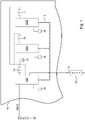
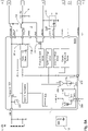
- Fig. 1 shows a portion of a printed circuit board (PCB) 10 populated with battery charging devices in accordance with the present disclosure.
- the PCB 10 may be a circuit board, for example, in a mobile computing device, a smart phone, and in general any electronic device.
- the PCB 10 may be populated with battery charging devices 102, 102a, 102b. It will be appreciated in the discussions to follow that fewer or more battery charging devices may be provided.
- Each of the battery charging devices 102, 102a, 102b may be embodied in any suitable integrated circuit (IC) packaging format (e.g., single in-line packaging, dual in-line packaging, surface mount devices, and so on) and interconnected on the PCB 10.
- IC integrated circuit
- the battery charging devices 102, 102a, 102b are identical devices that can be configured for different modes of operation.
- device 102 may be configured for "master" mode operation, while devices 102a, 102b may be configured for "slave” mode operation.
- battery charging devices 102, 102a, 102b may include pins or terminals (not shown) that allow the devices to be interconnected on the PCB 10 using PCB traces, represented generally by 12.
- the battery charging devices 102, 102a, 102b may be connected to a battery 22 via a connection 24 (e.g., battery terminal) for coordinated charging of the battery by the battery charging devices.
- the battery 22 may comprise any known configuration of one or more cells (e.g., a single-cell configuration, a multi-cell, multi-stack configuration, etc.) and may be use any suitable chemistry that allows for recharging.
- the battery charging devices 102, 102a, 102b operate as buck converters, and in other embodiments the battery charging devices may comprise buck-boost converters.
- the inductive component of the buck converter may be provided as external inductive elements 14 provided on the PCB 10. Accordingly, each battery charging device 102, 102a, 102b may be connected to a corresponding external inductive element 14, such as an inductor.
- the inductive elements 14 are "external" in the sense that they are not part of the charging ICs that comprise the battery charging devices 102, 102a, 102b.
- the capacitive component of the buck converters may be provided as an external capacitive element 16 on the PCB 10 that can be shared by each battery charging device 102, 102a, 102b.
- the capacitive element 16 is "external" in the sense that it is not part of the charging ICs that comprise the battery charging devices 102, 102a, 102b.
- each battery charging device 102, 102a, 102b may be connected to a corresponding external selection indicator 18 to configure the device for master or slave mode operation.
- Each selection indicator 18 is "external" in the sense that it is not part of the charging IC that comprises the device.
- the selection indicator 18 may be a resistive element.
- a connection to ground potential e.g., approximately 0 ⁇
- a non-zero resistance value e.g., 10K ⁇ , 100K ⁇ , etc.
- the selection indicator 18 may be a source of a suitable analog signal or digital signal that can serve to indicate to the device 102, 102a, 102b whether to operate in master mode or slave mode.
- Power to the battery charging devices 102, 102a, 102b may be externally provided via any suitable connector 26.
- the connector 26 may be a USB connector. Power from the VBUS line of a USB connector may be connected to device 102 (e.g., at a USBIN terminal), which may then distribute the power to the other devices 102a, 102b via a MIDUSBIN terminal.
- a USBIN terminal e.g., at a USBIN terminal
- Fig. 1A points out that the PCB 10 may be incorporated in any electronic device 50 to charge battery 22.
- Fig. 1B illustrates another configuration in which PCB 10 may be provided in a first electronic device 52 that has a connection 54 to a second electronic device 56 to charge battery 22 in the second electronic device.
- the connection 54 may not be physical, for example, wireless energy transfer from device 52 may be provided using magnetic induction circuitry (not shown).
- Fig. 2 shows a simplified schematic representation of the battery charging device 102.
- the battery charging device 102 may comprise a charging IC 202. It will be appreciated that in some implementations, the design of the charging IC may be implemented on two or more ICs. For purposes of discussion, however, we can assume a single charging IC implementation without loss of generality.
- the charging IC 202 may comprise circuitry to provide battery charging functionality in accordance with principles of the present disclosure.
- the battery charging functionality may be provided using a buck converter, or a buck-boost converter, and so on.
- the charging IC 202 may include a high-side FET 214a and a low-side FET 214b that can be configured in a buck converter topology in conjunction with inductive element 14 and capacitive element 16.
- a pulse width modulated (PWM) driver circuit may produce gate drive signals (HS, LS) at its switching output to switch the gates of respective FETs 214a and 214b.
- the PWM driver circuit may receive a current-mode control signal at its control input and a clock signal at its clock input to control the switching of FETs 214a and 214b.
- Power (Vph_pwr) from the buck converter may be connected to charge the battery 22 through battery FET 222 via the VSYS and CHGOUT terminals of the charging IC 202.
- the battery FET 222 may serve to monitor the charge current (e.g., using a charge current sense circuit).
- control signal may be internally generated within the charging IC 202 or externally provided to the charging IC.
- a feedback compensation network comprising various feedback control loops and a comparator 216 may serve as a source of an internally generated control signal.
- the feedback control loops may include an input current sense circuit (e.g., senses input current at USBIN), a charge current sense circuit (e.g., senses current at VSYS and CHGOUT terminals using battery FET 222), a system voltage sense circuit (e.g., senses voltage at VSYS terminal), a battery voltage sense circuit (e.g., senses battery voltage at VBATT terminal), and a battery temperature sense circuit (e.g., senses battery temperature at THERM terminal).
- the feedback control loops may comprise fewer, or additional, sense circuits.
- the comparator 216 may produce a reference that serves as the internally generated control signal.
- the control signal produced by comparator 216 is "internal" in the sense that the control signal is generated by circuitry that comprise the charging IC 202.
- a control signal is considered to be “externally” provided when the signal is received from a source external to the charging IC 202; e.g., via the CONTROL terminal of the charging IC.
- a control selector 216a may be provided to select either the internal control signal generated by the comparator 216 or an externally generated control signal received on the CONTROL terminal to serve as the control signal for the PWM driver circuit.
- the clock signal may be internally generated within the charging IC 202 or externally provided to the charging IC.
- the charging IC 202 may include a clock generator 218 to produce a clock signal (clock out).
- the clock generator 218 may include a clock generating circuit 218a and a delay element 218b.
- the clock generating circuit 218a may produce a clock signal that serves as an internally generated clock signal.
- the delay element 218b may receive an externally provided clock signal.
- the clock signal produced by the clock generating circuit 218a is "internal" in the sense that the clock signal is generated by circuitry that comprise the charging IC 202, namely the clock generating circuit.
- a clock signal is considered to be “externally” provided when the signal is received from a source external to the charging IC 202; e.g., via the CLK terminal of the charging IC.
- a clock selector 218c may be provided to select either the internal clock signal generated by the clock generating circuit 218a or an external clock signal provided on the CLK terminal and delayed (phase shifted) by the delay element 218b to serve as the clock signal for the PWM driver circuit.
- the charging IC 202 may include a selector circuit 212 to configure the charging IC to operate in "master" mode or "slave” mode according to the external selection indicator 18 provided on an SEL input of the charging IC.
- the selection indicator 18 may be a circuit, or a source of an analog signal (e.g., an analog signal generator) or a digital signal (e.g., digital logic). In some embodiments, for example, the selection indicator 18 may be an electrical connection to ground potential, either directly or through a resistive element.
- the selector circuit 212 may operate the control selector 216a and the clock selector 218c according to the selection indicator 18.
- the selector circuit 212 may also operate a switch 220 to enable or disable sensing of the current input in accordance with the selection indicator 18.
- the charging IC 202 may be configured as a single-phase standalone device, or used in a multi-phase configuration.
- the discussion will first describe a single-phase configuration.
- Fig. 3 illustrates an example of the charging IC 202 configured to operate as a standalone battery charger.
- the charging IC 202 may be configured using the SEL input to operate in master mode.
- master mode operation in charging IC 202 may be designated by a selection indicator 18 that comprises a connection of the SEL input to ground potential. This convention for designating master mode operation will be used for the remainder of the disclosure with the understanding that, in other embodiments, other conventions may be adopted to indicate master mode operation.
- the selector 212 may be configured to respond to the presence of a ground connection at the SEL input by configuring the charging IC 202 for master mode operation. For example, the selector 212 may operate the control selector 216a in a first configuration to provide an internally generated control signal to the control input of the PWM driver circuit. The internally generated control signal is also provided to the CONTROL terminal of charging IC 202, which for the single-phase configuration shown in Fig. 3 is not relevant.
- the selector 212 may operate the clock selector 218c in a first configuration to provide an internally generated clock signal (e.g., via clock generating circuit 218a) to the clock input of the PWM driver circuit.
- the internally generated clock signal is also provided to the CLK terminal of charging IC 202, which for the single-phase configuration shown in Fig. 3 is not relevant.
- the selector 212 may also operate switch 220 to a configuration that enables input current sensing on the power input USBIN.
- the master-mode configured charging IC 202 shown in Fig. 3 operates as a buck converter to charge battery 22.
- Feedback control to the PWM driver circuit is provided by the circuitry comprising the charging IC 202, and likewise, the clock signal to the circuit is provided from within the charging IC.
- the configuration is a "standalone" configuration in the sense that there is only one charging IC.
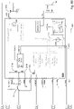
- a dual-phase configuration two charging ICs 202 are connected and operate together to charge a battery 22.
- One of the charging ICs 202 may be configured as a master device and the other as a slave device.
- Figs. 4A and 4B show an example of charging ICs 202a and 202b configured to operate respectively as a master device and as a slave device.
- the charging ICs 202a, 202b are connected together at connections A, B, C, D, E, F, and G.
- the resulting current flow is illustrated in Figs. 4A and 4B as flow 422.
- the charging IC 202a shown in Fig. 4A is configured for master mode operation as described in Fig. 3 .
- the control signal generated by the comparator 216 in charging IC 202a is provided as an externally generated control signal 402 (e.g., via the CONTROL terminal), in addition to serving as an internally generated control signal for the PWM driver circuit in the charging IC.
- the clock signal generated by the clock generator 218 is provided as an externally generated clock signal 404 (e.g., via the CLK terminal), in addition to serving as an internally generated clock signal for the PWM driver circuit in the charging IC 202a.
- the charging IC 202b is configured for slave mode operation.
- the charging IC 202b may be configured using the SEL input to operate in slave mode.
- slave mode operation may be designated by a selection indicator 18 that comprises a resistive element. This convention for designating slave mode operation will be used for the remainder of the disclosure with the understanding that, in other embodiments, other conventions may be adopted to indicate slave mode operation.
- a 10K resistor may be used to indicate slave mode operation. It will be appreciated, of course, that another resistance value may be used.
- the selector 212 may be configured to respond to the detection of a 10K ⁇ resistance at the SEL input by configuring the charging IC 202b for slave mode operation.
- the selector 212 may operate the control selector 216a in a second configuration to receive the externally generated control signal 402 that is received on the CONTROL terminal of the charging IC 202b.
- the control selector 216a provides the externally generated control signal 402 to the control input of the PWM driver circuit. Operation of the control selector 216a in the second configuration disconnects or otherwise effectively disables the feedback network in charging IC 202b from the PWM driver circuit. This "disconnection" is emphasized in the figure by illustrating the elements of the feedback network in charging IC 202b using broken grayed out lines.
- the selector 212 in charging IC 202b may also operate the clock selector 218c in a second configuration to receive the externally generated clock signal 404 on the CLK terminal.
- the clock selector 218c provides the externally generated clock signal 404 to the delay element 218b.
- the clock signal that is provided to the PWM driver circuit comes from the delay element 218b, thus disconnecting or otherwise effectively disabling the clock generating circuit 218a in the charging IC 202b.
- Switch 220 may be configured (e.g., by selector 212) to disable current sensing at the USBIN terminal of charging IC 202b.
- Power to the high- and low- side FETs 214a, 214b may be provided by the MIDUSBIN terminal via connection B.
- charge current sensing in the slave-configured charging IC 202b may be disabled by disabling its battery FET 222.
- operation of the PWM driver circuit in the slave-mode charging IC 202b is controlled by the control signal and clock signal that is generated in the master-mode charging IC 202a and provided to the slave-mode charging IC 202b respectively as externally generated control and clock signals 402, 404.
- the control and clock signals generated in the master-mode charging IC 202a are deemed to be "externally generated.”
- the master-mode charging IC 202a may synchronize with the slave-mode charging IC 202b by asserting a signal on the FETDRV terminal. For example, when the master-mode charging IC 202a pulls the FETDRV terminal LO, the PWM driver circuit in the slave-mode charging IC 202b is disabled. When the master-mode charging IC 202a pull the FETDRV terminal HI, the PWM driver circuit in the slave-mode charging IC 202b begins switching.
- the FETDRV terminal may be used by the master-mode charging IC 202a to initiate switching in the slave-mode charging IC 202b after the input current rises above a threshold level, in order to balance light-load and heavy-load efficiency.
- switching losses at light load can outweigh the decreased conduction losses, which can be avoided by not enabling the slave-mode charging IC 202b right away.
- the slave-mode charging IC 202b will operate in synchrony with the clock signal from the master-mode charging IC 202a.
- Control of the PWM driver circuit in the slave-mode charging IC 202b will be provided by the control signal from the master-mode charging IC 202a, thus allowing the master to set the charge current limit, input current limit, etc.
- the delay element 218b may be configured (e.g., by selector 212) to provide a selectable phase shift that is suitable for dual-phase operation.
- the delay element 218b may provide a 180° phase shift of the externally generated clock signal 404.
- the clock signal that is provided to the clock input of the PWM driver circuit in the slave-mode charging IC 202b is 180° out of phase relative to the clock signal in the master-mode charging IC 202a. Consequently, the charging cycle of the master-mode charging IC 202a will be 180° out of phase relative to the charging cycle of the slave-mode charging IC 202b.
- the high-side FET 214a is ON in the master device
- the high-side FET in the slave device is OFF, and vice-versa.
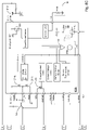
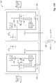
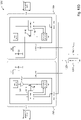
- FIG. 5A-5C show an example charging ICs 202a, 202b, and 202c configured to operate respectively as a master device, a first slave device, and a second slave device.
- the charging ICs 202a, 202b, 202c are connected at connections A1, B1, C1, D1, E1, F1, and G1 and connections A2, B2, C2, D2, E2, F2, and G2.
- the master device in Fig. 5A is configured as explained in connection with Fig. 4A .
- the first and second slave devices ( Figs. 5B and 5C ) are configured as explained in connection with Fig. 4B .
- the delay elements 218b in the first and second slave devices may be configured to provide 120° and 240° phase shifts, respectively, of the externally generated clock signal 404 as the clock input for the respective PWM driver circuits.
- the selection indicator 18 in the first slave device of Fig. 5B may be a 100K resistor to indicate 120° phase shift
- the selection indicator 18 in the second slave device of Fig. 5C may be a 1M resistor to indicated 240° phase shift.
- the charging cycle of the master device ( Fig. 5A ) will be 120° out of phase relative to the charging cycle of the first slave device ( Fig. 5B ) and 240° out of phase relative to the charging cycle of the second slave device ( Fig. 5C ).
- N-phase operation may be provided using N charging ICs (one master device and (N-1) slave devices) and connecting them in accordance with the examples shown in the figures.
- Each of the (N-1) slave devices receives from the master device the externally generated control signal 402 and the externally generated clock signal 404.
- the m th slave device may be configured (e.g., using a suitable selection indicator 18) to provide an m ⁇ (360 ⁇ N)° phase shift (e.g., using the delay element 218b) of the externally generated clock signal 404 as the clock input for its PWM driver circuit.
- the quantity ( m ⁇ N) is an integral multiple of 360.
- a charging IC may be implemented as a master-only device. In other words, the charging IC always operates in master mode and is not configurable to operate as a slave device.
- Fig. 6 shows a charging IC 602 comprising, among other components, a feedback network comprising several sensor components (e.g., input current sense, charge current sense, etc.) that feed into a comparator 616.
- the comparator output generates an internally generated control signal that feeds into the control input of the PWM driver circuit and which serves as an externally generated control signal 622 that is output at the CONTROL terminal.
- the charging IC 602 further comprises a clock 618 that generates a clock signal that generates an internally generated clock signal, which feeds into the clock in of the PWM driver circuit, and which serves as an externally generated clock signal 624 that is output at the CLK terminal.
- This particular example of charging IC always uses its internally generated control and clock signals and always outputs those signals as respective externally generated control and clock signals.
- the charging IC 602 can omit selector 212, selectors 216a, 218b, and 220, and the delay element 218b in order to realize a smaller, lower cost device.
- a charging IC may be implemented as a slave-only device.
- Fig. 7 shows a charging IC 702 comprising a PWM drive circuit having a control input that receives only an externally generated control signal 722 (e.g., from the CONTROL terminal).
- the PWM driver circuit furthermore, has a clock input that receives only an externally generated clock signal 724 (e.g., from the CLK terminal).
- the selector 712 serves to configure a delay element 718 to provide phase shifting of the externally generated clock signal 724 according to the selection indicator 18.
- the delay element 718 may be configured to provide an m ⁇ (360 ⁇ (M+1))° phase shift of the externally generated clock signal depending on what is connected to the selector 712, where m identifies the charging IC 702 as being the m th slave device among a total of M slave devices.
- the charging IC 702 is "slave-only" in the sense that it does not generate its control and clock signals internally, but rather obtains them from a source external to the charging IC. Since the control signal and clock signal are always externally generated, the slave-only charging IC 702 can omit the circuitry comprising the feedback network and the clock. Likewise, the slave-only charging IC 702 can omit the input FET and battery FET, since the device does not need to sense the input current. This can be advantageous in terms of a smaller device and/or a lower cost device, especially since the input and battery FETs are power FETs which can occupy significant areas on the die.
- the slave-only charging IC 702 may include additional circuitry to enhance performance. Though not illustrated, for example, a slave-only charging IC may include inductor current sense circuitry for peak current limiting. As another example, a slave-only charging IC may additionally include a thermal loop to ensure the junction temperature does not exceed a maximum operating limit.
- a charging IC in accordance with the present disclosure may further include a FETCRTL terminal.
- Fig. 8A shows the charging IC 802a configured as a dual-input master.
- the dual-input master configuration may be indicated with a selection indicator 18 that comprises a 100K ⁇ resistor.
- Fig. 8B shows the charging IC 802b configured as a dual-input slave, operating in slave mode.
- Fig. 8C shows the charging IC 802b operating in master mode.
- the dual-input slave configuration may be indicated using a selection indicator 18 that comprises a 200K ⁇ resistor.
- the configuration is "dual-input" in the sense that there are two voltage inputs.
- a first voltage input e.g., USBIN
- a second voltage input e.g., DCIN
- DCIN DCIN FET 812
- the dual-input configured charging ICs 802a and 802b operate in a master/slave mode as explained above.
- the dual-input master 802a generates a feedback control signal 802 that is used by the master and provided to the slave ( Fig. 8B ) via the CONTROL terminal.
- the dual-input master 802a generates a clock signal 804 that is used by the master and provided to the slave via the CLK terminal.
- the dual-input slave 802b shown in Fig. 8B uses the externally provided control signal 802 and clock signal 804 to control its PWM driver circuit.
- the dual-input master 802a asserts FETCTRL (e.g., goes high-z) to turn OFF the DCIN FET 812 that is connected to the dual-input slave 802b. This serves to electrically isolate the DCIN voltage source (if present) from the USBIN (DCIN) terminal of the dual-input slave 802b.
- the dual-input master 820a asserts FETDRV (e.g., pulls HIGH) to signal the dual-input slave 802b to operate in slave mode.
- the master When there is no voltage on the USBIN terminal of the dual-input master 802a, the master does not perform battery charging.
- the dual-input master 802a will assert FETCTRL (e.g., goes LOW) to turn ON the DCIN FET 812 to allow current flow from the DCIN voltage source.
- FETCTRL e.g., goes LOW
- the dual-input slave 802b operates in master mode to perform battery charging using the DCIN input provided on its USBIN terminal.
- This master operating mode of the dual-input slave 802b is illustrated in Fig. 8C .
- the dual-input slave 802b does not receive an external control signal or clock signal on its CONTROL and CLK terminals, since the dual-input master 802a is not performing battery charging. Instead, the dual-input slave 802b generates its own control and clock signals and performs battery charging from DCIN in master mode.
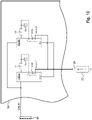
- Fig. 9 illustrates a dual-input charging IC 902 configured with a charging IC 904 configured for slave mode operation.
- the bounding box 900 is used to indicate that device 904 and a portion of device 902 are configured as illustrated in Figs. 4A and 4B .
- the device 902 may be configured to always operate in master mode.
- the device 904 may be configured with a selection indicator comprising a 1k ⁇ resistor to indicate that the slave may operate in on-the-go (OTG) mode.
- the devices 902, 904 may operate in master/slave mode to provide multi-phase charging of the battery 22 as explained in the foregoing embodiments.
- the device 904 may be signaled to operate in OTG mode.
- device 904 may include interface circuitry (not shown) to receive a command via the Inter-Integrated Circuit (I 2 C) communication protocol. It will be appreciated, of course, that any other suitable signaling may be used.
- I 2 C Inter-Integrated Circuit
- Fig. 9 illustrates the two different current flows 912, 914 in this "OTG" mode of operation.
- Flow 912 represents charging current from the dual-input charging IC 902 to charge battery 22.
- Flow 914 represents current from battery 22 to the USBIN terminal of device 902. It is noted that though control and clock signals from device 902 may be provided on its respective CONTROL and CLK terminals, the signals are not used by the device 904 in OTG mode.
- Fig. 10 shows another configuration of battery charging devices 1002a, 1002b in accordance with the present disclosure.
- the battery charging devices 1002a, 1002b may be configured as buck converters.
- the inductor L and output capacitor C of each battery charging device are depicted as external components, but in some embodiments they can be internal.
- Each battery charging device (e.g., 1002a) may include control circuitry 1012 to control its battery charging operation. Additional details of control circuitry 1012 will be given below.
- the battery charging device (e.g., 1002a) may be the SMB1357 switch-mode battery charging IC component, which is manufactured and sold by Qualcomm, Inc.
- the battery charging device may use the battery charging circuitry in the PMi8994 power management IC component, which is also manufactured and sold by Qualcomm, Inc.
- the battery charging device may include a STAT (status) output or other equivalent indicator.
- the STAT output may output a signal that indicates whether the battery charging device is charging (e.g., logic HI) or not charging (e.g., logic LO). For example, if the battery charging device detects a fault condition (e.g., over-temperature event, charge timer timing out, etc.), the device may cease battery charging and assert the STAT output accordingly.
- the STAT output may provide more information (digitally or in analog) than simply whether the battery charging device is charging or not; e.g., the STAT output may provide information indicative of a fault event.
- the battery charging device may include an EN input or other equivalent enable control input that enables or disables operation of the battery charging device. For example, a logic HI asserted on the EN input may enable operation of the battery charging device, while a logic LO may serve to disable operation of the battery charging device.
- a battery charging operation may be initiated by asserting the EN input. Subsequently de-asserting the EN input can be used to prematurely terminate or force quit a battery charging operation.
- Fig. 10 illustrates a configuration of battery charging devices 1002a, 1002b in accordance with some embodiments of the present disclosure.
- the charging outputs CHGOUT of battery charging devices 1002a, 1002b may be connectable to battery 22 via connection 24 (e.g., battery terminal).
- the STAT output of battery charging device 1002a may be connected to the EN input of battery charging device 1002b.
- Fig. 10A illustrates a configuration comprising three battery charging devices 1002a, 1002b, 1002c.
- the CHGOUT of each battery charging device 1002a - 1002c may be connected to battery 22 (e.g., via connection 24).
- the STAT output of battery charging device 1002a may be connected to the EN input of battery charging devices 1002b and 1002c.
- battery charging device 1002a may be referred to as the master or principle device and battery charging device 1002b
- battery charging device 1002c in Fig. 10A may be referred to as slave or secondary devices, for the reason that the master device can disable the slave devices using its STAT output; for example, in response to the master device detecting a fault event.
- the same part (e.g., SMB1357) may be used to implement each of the battery charging devices 1002a - 1002c.
- the battery charging devices 1002a - 1002c may be implemented using different parts; e.g., different parts from the same manufacturer, parts from different manufacturers, etc.
- the battery charging devices 1002a - 1002c can use any suitable switched mode voltage regulation design and in general can be configured with any suitable voltage regulation circuitry.
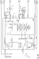
- Fig. 11 shows additional detail of a charging circuit 1102 in accordance with some embodiments of the present disclosure.
- the charging circuit 1102 may include a buck convert comprising a buck control circuit 1112 operating in conjunction with inductor L and capacitor C.
- the inductor L and capacitor C components may be provided on-chip in the charging circuit 1102.
- these components are external to the charging device 1102 for practical reasons such as the physical sizes of the components, in order to provide better performing devices (e.g., semiconductor inductors typically do not perform as well as magnetic core inductors), to allow for flexibility in design, and so on.
- the charging circuit 1102 may employ a voltage regulator other than a buck converter design.
- a controller 1114 may provide various control functions.
- the controller 1114 may receive input from other circuitry (not shown) such as a temperature sensor, timers, current sensors, etc.
- the controller 1114 may use the input to detect a fault event that may require ceasing or otherwise disabling battery charging.
- the controller 1114 may assert a signal on the STAT output (e.g., logic HI), for example, so that an electronic device (e.g., 50, Fig. 1 ) that incorporates the charging circuit 1102 can signal the user of the fault event.
- fault events may include excessive ambient temperature, a charging timer timing out, excessive current flow, battery disconnection during a charging operation, and so on.
- the controller 1114 may include or otherwise have access to a data store (not shown) to store a battery voltage threshold value 1114a.
- the data store may be a data register or other suitable data storage element.
- the controller 1114 may include a programming input (PGM) to program or otherwise set the battery threshold voltage value 1114a.
- PGM programming input
- the charging circuit 1102 may include a battery FET 1116 that is connected between the output V OUT of the buck converter and a charging output CHGOUT of the circuit, where the charging output can be connected to a battery to be charged.
- the battery FET 1116 may an n-channel device, and in other embodiments may be a p-channel device.
- the illustrative embodiment of Fig. 11 shows an NMOS type battery FET 1116.
- the drain terminal of the battery FET 1116 is connected to the output of the buck converter and the source terminal is connectable to a battery to be charged.
- the controller 1114 may include a control output that can be used to control the battery FET 1116, for example, by connecting the control output of the controller to the battery FET gate terminal. As will be explained below, the battery FET 1116 allows for control of a battery charging operation.
- the charging circuit 1102 may include a voltage sense circuit 1118 (voltage sensor) to sense or otherwise detect the battery voltage level of a battery to be charged.
- the battery voltage sense circuit 1118 may include a comparator 1122 to compare a battery voltage picked up by resistor divider network R1/R2 with a reference voltage 1124.
- the comparator output may be provided to the controller 1114 to control a battery charging operation based on the detected battery voltage level.
- the voltage reference 1124 may be programmable, and in some embodiments may be set by the controller 1114 according to the stored battery threshold voltage value 1114a.
- the battery charging operation may include a constant current charging state (constant current mode) followed by a constant voltage charging state (constant voltage mode).
- the controller 1114 may start the battery charging operation in the first charging state, constant current mode.
- the controller 1114 may subsequently switch the battery charging operation to the second charging state, constant voltage mode.
- the battery charging operation may include only a single charging state; e.g., constant current charging. In still other embodiments, the battery charging operation may include multiple states of charging.
- the controller 1114 may orchestrate the battery charging operation by controlling the buck converter to maintain a constant current output during constant current mode charging.
- the controller 1114 can monitor the battery condition (e.g., battery voltage) to determine when to switch to constant voltage charging, at which time the controller can control the buck converter to maintain a constant voltage output for constant voltage mode charging.
- the charging circuit 1102 may include a STAT output.
- the controller 1114 may monitor other conditions in the charging circuit 1102 for the occurrence of fault events.
- the controller 1114 may assert a suitable signal (digital or analog) on the STAT output in response to determining that a fault event has occurred.
- External circuitry in an electronic device that incorporates the charging circuit 1102 may process the signal accordingly; e.g., warn a user, trigger an alarm, etc.
- circuitry other than or in addition to the controller 1114 may detect fault events and assert the STAT output.
- the charging circuit 1102 may include an EN input. As explained above, the EN input may be used to tell the charging circuit 1102 whether or not a battery charging operation can be performed. Circuitry external to the charging circuit 1102 can assert a signal (digital or analog) on the EN input when battery charging is not desired. In some embodiments, the controller 1114 may receive the signal and disable the battery charging operation in response. In other embodiments, circuitry other than the controller 1114 may be employed.
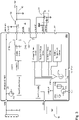
- Fig. 12 shows a battery charging circuit 1200 in accordance with the present disclosure, for example, using circuitry such as shown in Fig. 11 .
- the battery charging circuit 1200 may comprise charging circuits 1202 and 1204.
- the same device may used for the charging circuits 1202 and 1204.
- different devices may be used for charging circuits 1202 and 1204; for example, the devices need not be the same part, and may even be parts from different manufacturers.
- Fig. 12 shows charging circuit 1202 to be the same as charging circuit 1204.
- the battery charging circuit 1200 may include a battery terminal 1224 that is connectable to a battery to be charged 1222.
- the charging outputs CHGOUT of charging circuit 1202 and charging circuit 1204 may be connected together at battery terminal 1224.
- power from the buck converter of each charging circuit can be provided to the battery 1222.
- the STAT out of charging circuit 1202 may be connected to the EN input of charging circuit 1204.
- the charging circuit 1202 may be deemed the master or primary device, because charging circuit 1202 can disable charging circuit 1204 (slave or secondary device) when charging circuit 1202 detects a fault event and asserts a suitable signal on STAT out.
- the master device e.g., charging circuit 1202
- the slave device e.g., charging circuit 1204
- the master device is programmed with a battery threshold voltage value of 4.35 V and the slave device is programmed with a battery threshold voltage value of 4.33 V.
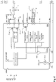
- the charging circuit 1200 when the battery charging circuit 1200 begins a battery charging operation (e.g., by asserting the EN inputs of both charging circuits 1202, 1204) the charging circuit can begin in a constant current charging state.
- the buck converter may operate in a constant current mode, operating effectively as a constant current source 1302 providing a current I, as depicted in the figure to battery 1222.
- current I from both charging circuits 1202, 1204 flows into battery 1222, thereby charging the battery.
- the current flow from each charging circuit 1202, 1204 may be the same. In other embodiments, the current flows may be different.
- the battery begins to charge and the battery voltage V BATT begins to rise.
- the controller 1114 may subsequently switch the next state of the battery charging operation. If there is only one charging state (e.g., constant current mode), then the next state is a termination state. In some embodiments, where the battery charging operation includes a constant current charging state and a constant voltage charging state, the controller 1114 can switch the battery charging operation from constant current charging to constant voltage charging.
- Fig. 13B illustrates an example of an embodiment in which the battery charging operation includes a constant current state and a constant voltage state.
- the master device (charging circuit 1202) is configured to have a battery threshold voltage value of 4.35V
- the slave device (charging circuit 1204) is configured with a battery threshold voltage value of 4.33V. Accordingly, as the battery voltage V BATT increases from less than 4.33V ( Fig. 13A ) to 4.33V and crosses 4.33V, the controller 1114 in the slave device can detect that crossing and in response can switch from constant current charging to constant voltage charging.
- the controller 1114 in the slave device can control operation of the buck converter to act as a constant voltage source 1304, as depicted in the figure, to provide a constant voltage output of 4.33V as determined, for example, based on the battery threshold voltage value that is set in the slave device.
- the buck converter in the master device continues to operate as a constant current source.
- the battery voltage V BATT continues to rise to a value greater than 4.33V.
- the resulting voltage difference across the source and drain of battery FET 1116 will create an increasing pinch-off effect that will eventually turn OFF the battery FET.
- the controller 1114 in the slave device detects this condition, it can terminate the battery charging operation in the slave device (e.g., disable the buck controller 1112). This condition is shown in Fig. 13C , where only the master device is performing the battery charging operation and the slave device is schematically depicted as being turned off.
- the master device will continue charging in constant current mode until the battery voltage V BATT passes the battery threshold voltage value.
- the controller 1114 in the master device in response to V BATT passing the battery threshold voltage value (e.g., 4.35V), the controller 1114 in the master device can switch from constant current charging to constant voltage charging.
- the controller 1114 can control operation of the buck converter in the master device to act as a constant voltage source 1304, as depicted in Fig. 13D , to provide a constant voltage output of 4.35V as determined, for example, based on the battery threshold voltage value.
- the controller 1114 may then terminate the battery charging operation after the batter voltage V BATT exceeds a final value.
- the battery charging circuit 1200 can comprise two or more slave devices. Each additional slave device can be configured with a battery threshold voltage value that is smaller than the other slave devices.
- the battery threshold voltage values for the slave devices may be 4.33 V and 4.31 V, and for the master circuit may be 4.35 V.
- the 4.31V slave circuit may switch over from constant current mode to constant voltage mode first, after the battery voltage reaches and exceeds 4.31 V. As the battery continues to charge, it's voltage will continue to rise. Pinch-off in the battery FET of the 4.31V slave circuit may cause that charging circuit to turn off, leaving the master circuit and the 4.33V slave circuit charging the battery.
- the battery will continue to charge and it's voltage will reach and exceed 4.33 V. This may cause the 4.33V slave circuit to switch over from constant current mode to constant voltage mode. As the battery continues to charge, it's voltage will continue to rise. Pinch-off in the battery FET of the 4.33V slave circuit may cause that charging circuit to turn off, leaving only the master circuit charging the battery. As explained above, eventually the master circuit will go into constant voltage mode and eventually turn off.
- Each of the charging circuits is capable of charging a battery.
- An advantageous aspect of the present disclosure is that the battery charging circuit can provide fast charging during constant current mode because two or more charging circuits (e.g., 1202, 1204) can be combined to contribute charging current to the battery. Since the slave device(s) (e.g., 1204) switches out of constant current mode and into constant voltage mode before the master device (e.g., 1202), the slave device turns off as explained above before the master device goes into constant voltage mode charging. This avoids the potential adverse effects of having two voltage sources connected to each other. The slave device turning off can ensure that there is only one constant voltage source in the circuit.
Landscapes
- Engineering & Computer Science (AREA)
- Power Engineering (AREA)
- Charge And Discharge Circuits For Batteries Or The Like (AREA)
- Secondary Cells (AREA)
Applications Claiming Priority (4)
| Application Number | Priority Date | Filing Date | Title |
|---|---|---|---|
| US201361827443P | 2013-05-24 | 2013-05-24 | |
| US14/065,752 US9276430B2 (en) | 2013-05-24 | 2013-10-29 | Master-slave multi-phase charging |
| US14/251,206 US9590436B2 (en) | 2013-05-24 | 2014-04-11 | Master-slave multi-phase charging |
| PCT/US2014/034002 WO2014189629A1 (en) | 2013-05-24 | 2014-04-14 | Master-slave multi-phase charging |
Publications (2)
| Publication Number | Publication Date |
|---|---|
| EP3005513A1 EP3005513A1 (en) | 2016-04-13 |
| EP3005513B1 true EP3005513B1 (en) | 2022-05-04 |
Family
ID=50733413
Family Applications (1)
| Application Number | Title | Priority Date | Filing Date |
|---|---|---|---|
| EP14724943.7A Active EP3005513B1 (en) | 2013-05-24 | 2014-04-14 | Master-slave multi-phase charging |
Country Status (6)
| Country | Link |
|---|---|
| US (1) | US9590436B2 (enExample) |
| EP (1) | EP3005513B1 (enExample) |
| JP (1) | JP6392327B2 (enExample) |
| KR (1) | KR102258589B1 (enExample) |
| CN (1) | CN105264734B (enExample) |
| WO (1) | WO2014189629A1 (enExample) |
Families Citing this family (35)
| Publication number | Priority date | Publication date | Assignee | Title |
|---|---|---|---|---|
| CN102868820A (zh) * | 2012-09-19 | 2013-01-09 | 中兴通讯股份有限公司 | 移动终端、数据通信主设备和移动终端充电系统及方法 |
| US9276430B2 (en) * | 2013-05-24 | 2016-03-01 | Qualcomm, Incorporated | Master-slave multi-phase charging |
| KR20150049961A (ko) * | 2013-10-31 | 2015-05-08 | 삼성전기주식회사 | 전력 공급 장치 |
| US9973017B2 (en) * | 2014-09-19 | 2018-05-15 | Samsung Electronics Co., Ltd. | Charger circuit including a plurality of charging paths |
| US9843211B2 (en) | 2014-09-22 | 2017-12-12 | Qualcomm Incorporated | Multiple power chargers for mobile terminals |
| CN104578372B (zh) * | 2015-01-15 | 2018-04-27 | 小米科技有限责任公司 | 控制终端设备充电的方法及装置 |
| KR101736475B1 (ko) * | 2015-02-04 | 2017-05-16 | 한화테크윈 주식회사 | 전기 차량 |
| US9977091B2 (en) * | 2015-04-28 | 2018-05-22 | Qualcomm Incorporated | Battery fuel gauges sharing current information between multiple battery chargers |
| US10396582B2 (en) * | 2015-07-01 | 2019-08-27 | Maxim Integrated Products, Inc. | Master slave charging architecture with communication between chargers |
| US9800152B2 (en) | 2015-07-06 | 2017-10-24 | Qualcomm Incorporated | Voltage regulator having auto mode optimized for load profiles |
| US10833518B2 (en) * | 2015-09-22 | 2020-11-10 | Guangdong Oppo Mobile Telecommunications Corp., Ltd. | Charge control method and device, and electronic device |
| US10326296B2 (en) | 2016-02-01 | 2019-06-18 | Qualcomm Incorporated | Dual-phase operation for concurrently charging a battery and powering a peripheral device |
| US20170222465A1 (en) * | 2016-02-01 | 2017-08-03 | Qualcomm Incorporated | Dynamic thermal balancing of parallel regulators to reduce hotspots and increase performance |
| CN105762865B (zh) | 2016-02-29 | 2019-02-01 | 宇龙计算机通信科技(深圳)有限公司 | 一种充电装置及充电方法 |
| US11088549B2 (en) * | 2016-03-22 | 2021-08-10 | Intersil Americas LLC | Multiple chargers configuration in one system |
| US10594152B1 (en) | 2016-03-25 | 2020-03-17 | Intersil Americas LLC | Method and system for a battery charger |
| CN110212599B (zh) | 2016-04-08 | 2022-12-27 | 华为技术有限公司 | 一种快速充电的方法、终端、充电器和系统 |
| CN106130124B (zh) * | 2016-07-29 | 2019-09-06 | 宇龙计算机通信科技(深圳)有限公司 | 一种实现多种快速充电协议兼容的方法、系统及终端 |
| WO2018090371A1 (zh) * | 2016-11-21 | 2018-05-24 | 深圳市柔宇科技有限公司 | 电子装置、充电器、充电系统及充电方法 |
| TWI614966B (zh) * | 2017-01-03 | 2018-02-11 | 飛宏科技股份有限公司 | 定電流模式之充電方法 |
| CN106786949A (zh) * | 2017-01-03 | 2017-05-31 | 奇酷互联网络科技(深圳)有限公司 | 终端设备及其对外充电方法 |
| KR20180079962A (ko) * | 2017-01-03 | 2018-07-11 | 삼성전자주식회사 | 로봇 청소기 및 그 제어 방법 |
| US10523042B2 (en) | 2017-05-12 | 2019-12-31 | Qualcomm Incorporated | Master-slave charging circuit with slave charger input current sensing and adaptive battery current limiting |
| US10587136B2 (en) * | 2017-07-06 | 2020-03-10 | Qualcomm Incorporated | Parallel charging architecture |
| US10734891B2 (en) | 2017-10-13 | 2020-08-04 | Qualcomm Incorporated | Power-up sequencing and high voltage protection for charge pump converters |
| US11171493B2 (en) | 2018-05-09 | 2021-11-09 | Qualcomm Incorporated | Wireless parallel charging |
| US10608455B2 (en) | 2018-05-18 | 2020-03-31 | Sling Media Pvt. Ltd. | Quick battery charging with protection based on regulation relative state of charge |
| US11606032B2 (en) | 2018-11-15 | 2023-03-14 | Qualcomm Incorporated | Adaptive combination power supply circuit and charging architecture |
| JP7319151B2 (ja) * | 2019-09-13 | 2023-08-01 | ローム株式会社 | ワイヤレス受電装置のコントロールic、電子機器 |
| KR102877560B1 (ko) | 2019-11-26 | 2025-10-28 | 삼성전자주식회사 | 전자 장치 및 이의 충전 방법 |
| KR102910364B1 (ko) * | 2020-04-13 | 2026-01-12 | 삼성전자 주식회사 | 병렬로 연결되는 다수 개의 배터리의 충전을 제어하기 위한 전자 장치 및 그의 동작 방법 |
| US11777330B2 (en) * | 2020-07-22 | 2023-10-03 | Microsoft Technology Licensing, Llc | Common charge controller for electronic devices with multiple batteries |
| CN114844135B (zh) * | 2021-02-02 | 2025-12-12 | 北京小米移动软件有限公司 | 一种充电方法、装置、终端及存储介质 |
| CN115037011A (zh) * | 2022-04-19 | 2022-09-09 | 伏达半导体(合肥)有限公司 | 双电池充电装置、方法及其控制器 |
| WO2024177237A1 (ko) * | 2023-02-22 | 2024-08-29 | 삼성전자 주식회사 | 배터리를 포함하는 전자 장치 및 제어 방법 |
Citations (2)
| Publication number | Priority date | Publication date | Assignee | Title |
|---|---|---|---|---|
| US20090160407A1 (en) * | 2007-12-24 | 2009-06-25 | Hwang Ho Chul | Charger Capable of Performing Integrated Control and Separate Control of Parallel Operations |
| US20120112705A1 (en) * | 2010-11-10 | 2012-05-10 | Richtek Technology Corporation, R.O.C. | Charger circuit |
Family Cites Families (29)
| Publication number | Priority date | Publication date | Assignee | Title |
|---|---|---|---|---|
| US4607208A (en) * | 1984-07-30 | 1986-08-19 | The United States Of America As Represented By The Secretary Of The Navy | Battery charger |
| JP3767024B2 (ja) | 1996-07-09 | 2006-04-19 | ソニー株式会社 | 充電装置 |
| JP2000278949A (ja) * | 1999-03-25 | 2000-10-06 | Origin Electric Co Ltd | コンデンサ充電器 |
| JP2000299136A (ja) * | 1999-04-15 | 2000-10-24 | Tdk Corp | バッテリ充電装置 |
| JP2004133719A (ja) * | 2002-10-11 | 2004-04-30 | Renesas Technology Corp | マイクロコンピュータ |
| US7135836B2 (en) * | 2003-03-28 | 2006-11-14 | Power Designers, Llc | Modular and reconfigurable rapid battery charger |
| US6836095B2 (en) | 2003-04-28 | 2004-12-28 | Semtech Corporation | Battery charging method and apparatus |
| JP4884665B2 (ja) * | 2004-11-12 | 2012-02-29 | ローム株式会社 | 直流−交流変換装置、そのコントローラic、及び直流−交流変換装置の並行運転システム |
| JP4847058B2 (ja) * | 2005-07-11 | 2011-12-28 | 株式会社ダイヘン | インバータ装置の並列運転方法 |
| US7522436B2 (en) | 2005-09-30 | 2009-04-21 | Volterra Semiconductor Corporation | Master-slave with adaptation control including slave current checking |
| DE102006013524B4 (de) * | 2006-03-23 | 2012-02-02 | Infineon Technologies Ag | Schaltwandler mit mehreren Wandlerstufen |
| EP1870979B1 (en) | 2006-06-21 | 2011-10-05 | Research In Motion Limited | Charging circuit for parallel charging multiple batteries |
| US7656132B2 (en) * | 2006-11-14 | 2010-02-02 | Advanced Analogic Technologies, Inc. | Battery charger apparatus with a digital charge reduction loop |
| US7777455B1 (en) * | 2007-06-19 | 2010-08-17 | Linear Technology Corporation | Switching battery charger with programmable current control and power control |
| JP2009011073A (ja) * | 2007-06-28 | 2009-01-15 | Panasonic Corp | スイッチング電源装置 |
| JP5205083B2 (ja) * | 2008-03-07 | 2013-06-05 | ルネサスエレクトロニクス株式会社 | 電源装置 |
| US8120205B2 (en) * | 2008-07-18 | 2012-02-21 | Zilker Labs, Inc. | Adding and dropping phases in current sharing |
| US8080981B2 (en) | 2009-11-06 | 2011-12-20 | Delta Electronics, Inc. | Interleaved-PWM power module system and method with phase-locking operation |
| JP5420433B2 (ja) | 2010-01-14 | 2014-02-19 | ルネサスエレクトロニクス株式会社 | 半導体装置および電源装置 |
| JP5455705B2 (ja) | 2010-02-25 | 2014-03-26 | Asti株式会社 | 充電装置と充電方法 |
| US20110304298A1 (en) * | 2010-05-13 | 2011-12-15 | Coda Automotive, Inc. | Battery charging using multiple chargers |
| US8319478B2 (en) * | 2010-08-16 | 2012-11-27 | Lear Corporation | Dual-charger system |
| JP5631173B2 (ja) | 2010-11-24 | 2014-11-26 | Asti株式会社 | 充電装置 |
| US8994338B2 (en) | 2011-01-14 | 2015-03-31 | Lear Corporation | Dual-charger system |
| US8441235B2 (en) | 2011-01-31 | 2013-05-14 | Taiwan Semiconductor Manufacturing Company, Ltd. | Battery charger digital control circuit and method |
| US8482340B2 (en) | 2011-11-04 | 2013-07-09 | Texas Instruments Incorporated | Master-slave low-noise charge pump circuit and method |
| KR102052590B1 (ko) * | 2012-11-22 | 2019-12-05 | 삼성에스디아이 주식회사 | 배터리 관리 시스템 및 그 구동 방법 |
| US9431838B2 (en) * | 2013-03-15 | 2016-08-30 | Integrated Device Technology, Inc. | Apparatuses and related methods for charging control of a switching voltage regulator |
| US9276430B2 (en) | 2013-05-24 | 2016-03-01 | Qualcomm, Incorporated | Master-slave multi-phase charging |
-
2014
- 2014-04-11 US US14/251,206 patent/US9590436B2/en active Active
- 2014-04-14 KR KR1020157035552A patent/KR102258589B1/ko active Active
- 2014-04-14 EP EP14724943.7A patent/EP3005513B1/en active Active
- 2014-04-14 JP JP2016515332A patent/JP6392327B2/ja active Active
- 2014-04-14 WO PCT/US2014/034002 patent/WO2014189629A1/en not_active Ceased
- 2014-04-14 CN CN201480028928.9A patent/CN105264734B/zh active Active
Patent Citations (2)
| Publication number | Priority date | Publication date | Assignee | Title |
|---|---|---|---|---|
| US20090160407A1 (en) * | 2007-12-24 | 2009-06-25 | Hwang Ho Chul | Charger Capable of Performing Integrated Control and Separate Control of Parallel Operations |
| US20120112705A1 (en) * | 2010-11-10 | 2012-05-10 | Richtek Technology Corporation, R.O.C. | Charger circuit |
Also Published As
| Publication number | Publication date |
|---|---|
| JP2016524284A (ja) | 2016-08-12 |
| EP3005513A1 (en) | 2016-04-13 |
| US20140347003A1 (en) | 2014-11-27 |
| US9590436B2 (en) | 2017-03-07 |
| CN105264734B (zh) | 2018-11-23 |
| CN105264734A (zh) | 2016-01-20 |
| KR102258589B1 (ko) | 2021-05-28 |
| WO2014189629A1 (en) | 2014-11-27 |
| JP6392327B2 (ja) | 2018-09-19 |
| KR20160012164A (ko) | 2016-02-02 |
Similar Documents
| Publication | Publication Date | Title |
|---|---|---|
| EP3005513B1 (en) | Master-slave multi-phase charging | |
| EP3005514B1 (en) | Master-slave multi-phase charging | |
| US10326296B2 (en) | Dual-phase operation for concurrently charging a battery and powering a peripheral device | |
| US20180074564A1 (en) | Reverse high-voltage power transfer | |
| CN107959421B (zh) | Buck-boost型直流转换器及其控制方法 | |
| Hwang et al. | 21.8 An all-in-one (Qi, PMA and A4WP) 2.5 W fully integrated wireless battery charger IC for wearable applications | |
| CN110915094B (zh) | 并行充电架构 | |
| US20170222465A1 (en) | Dynamic thermal balancing of parallel regulators to reduce hotspots and increase performance | |
| US10447161B2 (en) | Inverting buck-boost power converter | |
| TWI883127B (zh) | 充電裝置及充電系統 | |
| EP4362301A1 (en) | Voltage converter and power supply including the same | |
| Wang et al. | A 1.5 A 88.6% Li-ion battery charger design using pulse swallow technique in light load | |
| US20240178759A1 (en) | Electrical device including bidirectional switching converter | |
| TW202537214A (zh) | 用於操作多位準轉換器電路的系統、方法及積體電路 | |
| Huang et al. | A fast and high efficiency buck converter with switch-on-demand modulator for wide load range applications | |
| TW202610207A (zh) | 多位準轉換器電路、用於多位準轉換器電路的系統以及操作多位準轉換器電路的方法 | |
| WO2025151810A1 (en) | Multi-level reverse current blocking systems and methods | |
| TW202534466A (zh) | 用於操作多位準轉換器電路的系統 | |
| TW202537209A (zh) | 用於操作多位準轉換器電路的積體電路、方法及電路 |
Legal Events
| Date | Code | Title | Description |
|---|---|---|---|
| PUAI | Public reference made under article 153(3) epc to a published international application that has entered the european phase |
Free format text: ORIGINAL CODE: 0009012 |
|
| 17P | Request for examination filed |
Effective date: 20151020 |
|
| AK | Designated contracting states |
Kind code of ref document: A1 Designated state(s): AL AT BE BG CH CY CZ DE DK EE ES FI FR GB GR HR HU IE IS IT LI LT LU LV MC MK MT NL NO PL PT RO RS SE SI SK SM TR |
|
| AX | Request for extension of the european patent |
Extension state: BA ME |
|
| DAX | Request for extension of the european patent (deleted) | ||
| STAA | Information on the status of an ep patent application or granted ep patent |
Free format text: STATUS: EXAMINATION IS IN PROGRESS |
|
| 17Q | First examination report despatched |
Effective date: 20180418 |
|
| RIC1 | Information provided on ipc code assigned before grant |
Ipc: H02J 7/04 20060101ALI20210518BHEP Ipc: H02J 7/02 20160101ALI20210518BHEP Ipc: H02J 1/10 20060101AFI20210518BHEP |
|
| GRAP | Despatch of communication of intention to grant a patent |
Free format text: ORIGINAL CODE: EPIDOSNIGR1 |
|
| STAA | Information on the status of an ep patent application or granted ep patent |
Free format text: STATUS: GRANT OF PATENT IS INTENDED |
|
| INTG | Intention to grant announced |
Effective date: 20210701 |
|
| GRAJ | Information related to disapproval of communication of intention to grant by the applicant or resumption of examination proceedings by the epo deleted |
Free format text: ORIGINAL CODE: EPIDOSDIGR1 |
|
| STAA | Information on the status of an ep patent application or granted ep patent |
Free format text: STATUS: EXAMINATION IS IN PROGRESS |
|
| INTC | Intention to grant announced (deleted) | ||
| RIC1 | Information provided on ipc code assigned before grant |
Ipc: H02J 7/04 20060101ALI20211006BHEP Ipc: H02J 7/02 20160101ALI20211006BHEP Ipc: H02J 7/00 20060101ALI20211006BHEP Ipc: H02J 1/10 20060101AFI20211006BHEP |
|
| GRAP | Despatch of communication of intention to grant a patent |
Free format text: ORIGINAL CODE: EPIDOSNIGR1 |
|
| STAA | Information on the status of an ep patent application or granted ep patent |
Free format text: STATUS: GRANT OF PATENT IS INTENDED |
|
| INTG | Intention to grant announced |
Effective date: 20211124 |
|
| GRAS | Grant fee paid |
Free format text: ORIGINAL CODE: EPIDOSNIGR3 |
|
| GRAA | (expected) grant |
Free format text: ORIGINAL CODE: 0009210 |
|
| STAA | Information on the status of an ep patent application or granted ep patent |
Free format text: STATUS: THE PATENT HAS BEEN GRANTED |
|
| AK | Designated contracting states |
Kind code of ref document: B1 Designated state(s): AL AT BE BG CH CY CZ DE DK EE ES FI FR GB GR HR HU IE IS IT LI LT LU LV MC MK MT NL NO PL PT RO RS SE SI SK SM TR |
|
| REG | Reference to a national code |
Ref country code: GB Ref legal event code: FG4D |
|
| REG | Reference to a national code |
Ref country code: CH Ref legal event code: EP |
|
| REG | Reference to a national code |
Ref country code: AT Ref legal event code: REF Ref document number: 1490149 Country of ref document: AT Kind code of ref document: T Effective date: 20220515 |
|
| REG | Reference to a national code |
Ref country code: DE Ref legal event code: R096 Ref document number: 602014083534 Country of ref document: DE |
|
| REG | Reference to a national code |
Ref country code: IE Ref legal event code: FG4D |
|
| REG | Reference to a national code |
Ref country code: LT Ref legal event code: MG9D |
|
| REG | Reference to a national code |
Ref country code: NL Ref legal event code: MP Effective date: 20220504 |
|
| REG | Reference to a national code |
Ref country code: AT Ref legal event code: MK05 Ref document number: 1490149 Country of ref document: AT Kind code of ref document: T Effective date: 20220504 |
|
| PG25 | Lapsed in a contracting state [announced via postgrant information from national office to epo] |
Ref country code: SE Free format text: LAPSE BECAUSE OF FAILURE TO SUBMIT A TRANSLATION OF THE DESCRIPTION OR TO PAY THE FEE WITHIN THE PRESCRIBED TIME-LIMIT Effective date: 20220504 Ref country code: PT Free format text: LAPSE BECAUSE OF FAILURE TO SUBMIT A TRANSLATION OF THE DESCRIPTION OR TO PAY THE FEE WITHIN THE PRESCRIBED TIME-LIMIT Effective date: 20220905 Ref country code: NO Free format text: LAPSE BECAUSE OF FAILURE TO SUBMIT A TRANSLATION OF THE DESCRIPTION OR TO PAY THE FEE WITHIN THE PRESCRIBED TIME-LIMIT Effective date: 20220804 Ref country code: NL Free format text: LAPSE BECAUSE OF FAILURE TO SUBMIT A TRANSLATION OF THE DESCRIPTION OR TO PAY THE FEE WITHIN THE PRESCRIBED TIME-LIMIT Effective date: 20220504 Ref country code: LT Free format text: LAPSE BECAUSE OF FAILURE TO SUBMIT A TRANSLATION OF THE DESCRIPTION OR TO PAY THE FEE WITHIN THE PRESCRIBED TIME-LIMIT Effective date: 20220504 Ref country code: HR Free format text: LAPSE BECAUSE OF FAILURE TO SUBMIT A TRANSLATION OF THE DESCRIPTION OR TO PAY THE FEE WITHIN THE PRESCRIBED TIME-LIMIT Effective date: 20220504 Ref country code: GR Free format text: LAPSE BECAUSE OF FAILURE TO SUBMIT A TRANSLATION OF THE DESCRIPTION OR TO PAY THE FEE WITHIN THE PRESCRIBED TIME-LIMIT Effective date: 20220805 Ref country code: FI Free format text: LAPSE BECAUSE OF FAILURE TO SUBMIT A TRANSLATION OF THE DESCRIPTION OR TO PAY THE FEE WITHIN THE PRESCRIBED TIME-LIMIT Effective date: 20220504 Ref country code: ES Free format text: LAPSE BECAUSE OF FAILURE TO SUBMIT A TRANSLATION OF THE DESCRIPTION OR TO PAY THE FEE WITHIN THE PRESCRIBED TIME-LIMIT Effective date: 20220504 Ref country code: BG Free format text: LAPSE BECAUSE OF FAILURE TO SUBMIT A TRANSLATION OF THE DESCRIPTION OR TO PAY THE FEE WITHIN THE PRESCRIBED TIME-LIMIT Effective date: 20220804 Ref country code: AT Free format text: LAPSE BECAUSE OF FAILURE TO SUBMIT A TRANSLATION OF THE DESCRIPTION OR TO PAY THE FEE WITHIN THE PRESCRIBED TIME-LIMIT Effective date: 20220504 |
|
| PG25 | Lapsed in a contracting state [announced via postgrant information from national office to epo] |
Ref country code: RS Free format text: LAPSE BECAUSE OF FAILURE TO SUBMIT A TRANSLATION OF THE DESCRIPTION OR TO PAY THE FEE WITHIN THE PRESCRIBED TIME-LIMIT Effective date: 20220504 Ref country code: PL Free format text: LAPSE BECAUSE OF FAILURE TO SUBMIT A TRANSLATION OF THE DESCRIPTION OR TO PAY THE FEE WITHIN THE PRESCRIBED TIME-LIMIT Effective date: 20220504 Ref country code: LV Free format text: LAPSE BECAUSE OF FAILURE TO SUBMIT A TRANSLATION OF THE DESCRIPTION OR TO PAY THE FEE WITHIN THE PRESCRIBED TIME-LIMIT Effective date: 20220504 Ref country code: IS Free format text: LAPSE BECAUSE OF FAILURE TO SUBMIT A TRANSLATION OF THE DESCRIPTION OR TO PAY THE FEE WITHIN THE PRESCRIBED TIME-LIMIT Effective date: 20220904 |
|
| PG25 | Lapsed in a contracting state [announced via postgrant information from national office to epo] |
Ref country code: SM Free format text: LAPSE BECAUSE OF FAILURE TO SUBMIT A TRANSLATION OF THE DESCRIPTION OR TO PAY THE FEE WITHIN THE PRESCRIBED TIME-LIMIT Effective date: 20220504 Ref country code: SK Free format text: LAPSE BECAUSE OF FAILURE TO SUBMIT A TRANSLATION OF THE DESCRIPTION OR TO PAY THE FEE WITHIN THE PRESCRIBED TIME-LIMIT Effective date: 20220504 Ref country code: RO Free format text: LAPSE BECAUSE OF FAILURE TO SUBMIT A TRANSLATION OF THE DESCRIPTION OR TO PAY THE FEE WITHIN THE PRESCRIBED TIME-LIMIT Effective date: 20220504 Ref country code: EE Free format text: LAPSE BECAUSE OF FAILURE TO SUBMIT A TRANSLATION OF THE DESCRIPTION OR TO PAY THE FEE WITHIN THE PRESCRIBED TIME-LIMIT Effective date: 20220504 Ref country code: DK Free format text: LAPSE BECAUSE OF FAILURE TO SUBMIT A TRANSLATION OF THE DESCRIPTION OR TO PAY THE FEE WITHIN THE PRESCRIBED TIME-LIMIT Effective date: 20220504 Ref country code: CZ Free format text: LAPSE BECAUSE OF FAILURE TO SUBMIT A TRANSLATION OF THE DESCRIPTION OR TO PAY THE FEE WITHIN THE PRESCRIBED TIME-LIMIT Effective date: 20220504 |
|
| REG | Reference to a national code |
Ref country code: DE Ref legal event code: R097 Ref document number: 602014083534 Country of ref document: DE |
|
| PLBE | No opposition filed within time limit |
Free format text: ORIGINAL CODE: 0009261 |
|
| STAA | Information on the status of an ep patent application or granted ep patent |
Free format text: STATUS: NO OPPOSITION FILED WITHIN TIME LIMIT |
|
| PG25 | Lapsed in a contracting state [announced via postgrant information from national office to epo] |
Ref country code: AL Free format text: LAPSE BECAUSE OF FAILURE TO SUBMIT A TRANSLATION OF THE DESCRIPTION OR TO PAY THE FEE WITHIN THE PRESCRIBED TIME-LIMIT Effective date: 20220504 |
|
| 26N | No opposition filed |
Effective date: 20230207 |
|
| PG25 | Lapsed in a contracting state [announced via postgrant information from national office to epo] |
Ref country code: SI Free format text: LAPSE BECAUSE OF FAILURE TO SUBMIT A TRANSLATION OF THE DESCRIPTION OR TO PAY THE FEE WITHIN THE PRESCRIBED TIME-LIMIT Effective date: 20220504 |
|
| REG | Reference to a national code |
Ref country code: CH Ref legal event code: PL |
|
| PG25 | Lapsed in a contracting state [announced via postgrant information from national office to epo] |
Ref country code: LU Free format text: LAPSE BECAUSE OF NON-PAYMENT OF DUE FEES Effective date: 20230414 |
|
| REG | Reference to a national code |
Ref country code: BE Ref legal event code: MM Effective date: 20230430 |
|
| PG25 | Lapsed in a contracting state [announced via postgrant information from national office to epo] |
Ref country code: MC Free format text: LAPSE BECAUSE OF FAILURE TO SUBMIT A TRANSLATION OF THE DESCRIPTION OR TO PAY THE FEE WITHIN THE PRESCRIBED TIME-LIMIT Effective date: 20220504 |
|
| PG25 | Lapsed in a contracting state [announced via postgrant information from national office to epo] |
Ref country code: MC Free format text: LAPSE BECAUSE OF FAILURE TO SUBMIT A TRANSLATION OF THE DESCRIPTION OR TO PAY THE FEE WITHIN THE PRESCRIBED TIME-LIMIT Effective date: 20220504 Ref country code: LI Free format text: LAPSE BECAUSE OF NON-PAYMENT OF DUE FEES Effective date: 20230430 Ref country code: IT Free format text: LAPSE BECAUSE OF FAILURE TO SUBMIT A TRANSLATION OF THE DESCRIPTION OR TO PAY THE FEE WITHIN THE PRESCRIBED TIME-LIMIT Effective date: 20220504 Ref country code: CH Free format text: LAPSE BECAUSE OF NON-PAYMENT OF DUE FEES Effective date: 20230430 |
|
| REG | Reference to a national code |
Ref country code: IE Ref legal event code: MM4A |
|
| PG25 | Lapsed in a contracting state [announced via postgrant information from national office to epo] |
Ref country code: BE Free format text: LAPSE BECAUSE OF NON-PAYMENT OF DUE FEES Effective date: 20230430 |
|
| PG25 | Lapsed in a contracting state [announced via postgrant information from national office to epo] |
Ref country code: IE Free format text: LAPSE BECAUSE OF NON-PAYMENT OF DUE FEES Effective date: 20230414 |
|
| PG25 | Lapsed in a contracting state [announced via postgrant information from national office to epo] |
Ref country code: IE Free format text: LAPSE BECAUSE OF NON-PAYMENT OF DUE FEES Effective date: 20230414 |
|
| PG25 | Lapsed in a contracting state [announced via postgrant information from national office to epo] |
Ref country code: BG Free format text: LAPSE BECAUSE OF FAILURE TO SUBMIT A TRANSLATION OF THE DESCRIPTION OR TO PAY THE FEE WITHIN THE PRESCRIBED TIME-LIMIT Effective date: 20220504 |
|
| PG25 | Lapsed in a contracting state [announced via postgrant information from national office to epo] |
Ref country code: BG Free format text: LAPSE BECAUSE OF FAILURE TO SUBMIT A TRANSLATION OF THE DESCRIPTION OR TO PAY THE FEE WITHIN THE PRESCRIBED TIME-LIMIT Effective date: 20220504 |
|
| PGFP | Annual fee paid to national office [announced via postgrant information from national office to epo] |
Ref country code: DE Payment date: 20250317 Year of fee payment: 12 |
|
| PG25 | Lapsed in a contracting state [announced via postgrant information from national office to epo] |
Ref country code: CY Free format text: LAPSE BECAUSE OF FAILURE TO SUBMIT A TRANSLATION OF THE DESCRIPTION OR TO PAY THE FEE WITHIN THE PRESCRIBED TIME-LIMIT; INVALID AB INITIO Effective date: 20140414 |
|
| PG25 | Lapsed in a contracting state [announced via postgrant information from national office to epo] |
Ref country code: HU Free format text: LAPSE BECAUSE OF FAILURE TO SUBMIT A TRANSLATION OF THE DESCRIPTION OR TO PAY THE FEE WITHIN THE PRESCRIBED TIME-LIMIT; INVALID AB INITIO Effective date: 20140414 |
|
| PG25 | Lapsed in a contracting state [announced via postgrant information from national office to epo] |
Ref country code: TR Free format text: LAPSE BECAUSE OF FAILURE TO SUBMIT A TRANSLATION OF THE DESCRIPTION OR TO PAY THE FEE WITHIN THE PRESCRIBED TIME-LIMIT Effective date: 20220504 |
|
| PGFP | Annual fee paid to national office [announced via postgrant information from national office to epo] |
Ref country code: GB Payment date: 20260320 Year of fee payment: 13 |
|
| PGFP | Annual fee paid to national office [announced via postgrant information from national office to epo] |
Ref country code: FR Payment date: 20260317 Year of fee payment: 13 |