EP3000550A2 - Soldering iron with automatic soldering connection validation - Google Patents
Soldering iron with automatic soldering connection validation Download PDFInfo
- Publication number
- EP3000550A2 EP3000550A2 EP15179757.8A EP15179757A EP3000550A2 EP 3000550 A2 EP3000550 A2 EP 3000550A2 EP 15179757 A EP15179757 A EP 15179757A EP 3000550 A2 EP3000550 A2 EP 3000550A2
- Authority
- EP
- European Patent Office
- Prior art keywords
- soldering
- barrel
- solder
- joint
- tip
- Prior art date
- Legal status (The legal status is an assumption and is not a legal conclusion. Google has not performed a legal analysis and makes no representation as to the accuracy of the status listed.)
- Granted
Links
- 238000005476 soldering Methods 0.000 title claims abstract description 192
- XEEYBQQBJWHFJM-UHFFFAOYSA-N Iron Chemical compound [Fe] XEEYBQQBJWHFJM-UHFFFAOYSA-N 0.000 title claims abstract description 76
- 229910052742 iron Inorganic materials 0.000 title claims abstract description 38
- 238000010200 validation analysis Methods 0.000 title claims abstract description 21
- 238000000034 method Methods 0.000 claims abstract description 49
- 238000001816 cooling Methods 0.000 claims abstract description 11
- 238000012544 monitoring process Methods 0.000 claims abstract description 5
- 229910000679 solder Inorganic materials 0.000 claims description 102
- 238000001514 detection method Methods 0.000 claims description 9
- 230000006870 function Effects 0.000 claims description 9
- 239000000463 material Substances 0.000 claims description 8
- 230000003213 activating effect Effects 0.000 claims description 2
- 230000008569 process Effects 0.000 description 27
- 230000008859 change Effects 0.000 description 7
- 230000009471 action Effects 0.000 description 5
- 229910052802 copper Inorganic materials 0.000 description 5
- 239000010949 copper Substances 0.000 description 5
- 239000000758 substrate Substances 0.000 description 5
- RYGMFSIKBFXOCR-UHFFFAOYSA-N Copper Chemical compound [Cu] RYGMFSIKBFXOCR-UHFFFAOYSA-N 0.000 description 4
- 238000012546 transfer Methods 0.000 description 3
- 229910018471 Cu6Sn5 Inorganic materials 0.000 description 2
- 230000015572 biosynthetic process Effects 0.000 description 2
- 238000006243 chemical reaction Methods 0.000 description 2
- 230000003247 decreasing effect Effects 0.000 description 2
- 238000010586 diagram Methods 0.000 description 2
- 239000007788 liquid Substances 0.000 description 2
- 230000005389 magnetism Effects 0.000 description 2
- 238000004519 manufacturing process Methods 0.000 description 2
- 238000002844 melting Methods 0.000 description 2
- 230000008018 melting Effects 0.000 description 2
- 238000012986 modification Methods 0.000 description 2
- 230000004048 modification Effects 0.000 description 2
- 238000012795 verification Methods 0.000 description 2
- 238000005303 weighing Methods 0.000 description 2
- 229910018082 Cu3Sn Inorganic materials 0.000 description 1
- 230000006978 adaptation Effects 0.000 description 1
- 229910045601 alloy Inorganic materials 0.000 description 1
- 239000000956 alloy Substances 0.000 description 1
- 238000004458 analytical method Methods 0.000 description 1
- 230000006399 behavior Effects 0.000 description 1
- 230000008901 benefit Effects 0.000 description 1
- 238000004364 calculation method Methods 0.000 description 1
- 238000004891 communication Methods 0.000 description 1
- 239000013078 crystal Substances 0.000 description 1
- 230000007423 decrease Effects 0.000 description 1
- 230000000694 effects Effects 0.000 description 1
- 238000005516 engineering process Methods 0.000 description 1
- 239000011521 glass Substances 0.000 description 1
- 229910000765 intermetallic Inorganic materials 0.000 description 1
- 238000012886 linear function Methods 0.000 description 1
- 238000005259 measurement Methods 0.000 description 1
- 229910052751 metal Inorganic materials 0.000 description 1
- 239000002184 metal Substances 0.000 description 1
- 150000002739 metals Chemical class 0.000 description 1
- 239000000203 mixture Substances 0.000 description 1
- 230000003647 oxidation Effects 0.000 description 1
- 238000007254 oxidation reaction Methods 0.000 description 1
- 238000012805 post-processing Methods 0.000 description 1
- 238000011084 recovery Methods 0.000 description 1
- 230000001105 regulatory effect Effects 0.000 description 1
- 230000008439 repair process Effects 0.000 description 1
- 239000011435 rock Substances 0.000 description 1
- 229910052709 silver Inorganic materials 0.000 description 1
- 239000000126 substance Substances 0.000 description 1
- 238000012360 testing method Methods 0.000 description 1
- 229910052718 tin Inorganic materials 0.000 description 1
- 238000012549 training Methods 0.000 description 1
- 230000001052 transient effect Effects 0.000 description 1
- 230000000007 visual effect Effects 0.000 description 1
Images


Classifications
-
- H—ELECTRICITY
- H05—ELECTRIC TECHNIQUES NOT OTHERWISE PROVIDED FOR
- H05K—PRINTED CIRCUITS; CASINGS OR CONSTRUCTIONAL DETAILS OF ELECTRIC APPARATUS; MANUFACTURE OF ASSEMBLAGES OF ELECTRICAL COMPONENTS
- H05K3/00—Apparatus or processes for manufacturing printed circuits
- H05K3/30—Assembling printed circuits with electric components, e.g. with resistor
- H05K3/32—Assembling printed circuits with electric components, e.g. with resistor electrically connecting electric components or wires to printed circuits
- H05K3/34—Assembling printed circuits with electric components, e.g. with resistor electrically connecting electric components or wires to printed circuits by soldering
- H05K3/341—Surface mounted components
- H05K3/3421—Leaded components
-
- B—PERFORMING OPERATIONS; TRANSPORTING
- B23—MACHINE TOOLS; METAL-WORKING NOT OTHERWISE PROVIDED FOR
- B23K—SOLDERING OR UNSOLDERING; WELDING; CLADDING OR PLATING BY SOLDERING OR WELDING; CUTTING BY APPLYING HEAT LOCALLY, e.g. FLAME CUTTING; WORKING BY LASER BEAM
- B23K3/00—Tools, devices, or special appurtenances for soldering, e.g. brazing, or unsoldering, not specially adapted for particular methods
- B23K3/02—Soldering irons; Bits
- B23K3/027—Holders for soldering irons
-
- H—ELECTRICITY
- H05—ELECTRIC TECHNIQUES NOT OTHERWISE PROVIDED FOR
- H05K—PRINTED CIRCUITS; CASINGS OR CONSTRUCTIONAL DETAILS OF ELECTRIC APPARATUS; MANUFACTURE OF ASSEMBLAGES OF ELECTRICAL COMPONENTS
- H05K13/00—Apparatus or processes specially adapted for manufacturing or adjusting assemblages of electric components
- H05K13/08—Monitoring manufacture of assemblages
-
- B—PERFORMING OPERATIONS; TRANSPORTING
- B23—MACHINE TOOLS; METAL-WORKING NOT OTHERWISE PROVIDED FOR
- B23K—SOLDERING OR UNSOLDERING; WELDING; CLADDING OR PLATING BY SOLDERING OR WELDING; CUTTING BY APPLYING HEAT LOCALLY, e.g. FLAME CUTTING; WORKING BY LASER BEAM
- B23K1/00—Soldering, e.g. brazing, or unsoldering
- B23K1/0008—Soldering, e.g. brazing, or unsoldering specially adapted for particular articles or work
- B23K1/0016—Brazing of electronic components
-
- B—PERFORMING OPERATIONS; TRANSPORTING
- B23—MACHINE TOOLS; METAL-WORKING NOT OTHERWISE PROVIDED FOR
- B23K—SOLDERING OR UNSOLDERING; WELDING; CLADDING OR PLATING BY SOLDERING OR WELDING; CUTTING BY APPLYING HEAT LOCALLY, e.g. FLAME CUTTING; WORKING BY LASER BEAM
- B23K3/00—Tools, devices, or special appurtenances for soldering, e.g. brazing, or unsoldering, not specially adapted for particular methods
- B23K3/02—Soldering irons; Bits
- B23K3/025—Bits or tips
-
- B—PERFORMING OPERATIONS; TRANSPORTING
- B23—MACHINE TOOLS; METAL-WORKING NOT OTHERWISE PROVIDED FOR
- B23K—SOLDERING OR UNSOLDERING; WELDING; CLADDING OR PLATING BY SOLDERING OR WELDING; CUTTING BY APPLYING HEAT LOCALLY, e.g. FLAME CUTTING; WORKING BY LASER BEAM
- B23K3/00—Tools, devices, or special appurtenances for soldering, e.g. brazing, or unsoldering, not specially adapted for particular methods
- B23K3/02—Soldering irons; Bits
- B23K3/03—Soldering irons; Bits electrically heated
- B23K3/033—Soldering irons; Bits electrically heated comprising means for controlling or selecting the temperature or power
-
- B—PERFORMING OPERATIONS; TRANSPORTING
- B23—MACHINE TOOLS; METAL-WORKING NOT OTHERWISE PROVIDED FOR
- B23K—SOLDERING OR UNSOLDERING; WELDING; CLADDING OR PLATING BY SOLDERING OR WELDING; CUTTING BY APPLYING HEAT LOCALLY, e.g. FLAME CUTTING; WORKING BY LASER BEAM
- B23K3/00—Tools, devices, or special appurtenances for soldering, e.g. brazing, or unsoldering, not specially adapted for particular methods
- B23K3/08—Auxiliary devices therefor
-
- B—PERFORMING OPERATIONS; TRANSPORTING
- B23—MACHINE TOOLS; METAL-WORKING NOT OTHERWISE PROVIDED FOR
- B23K—SOLDERING OR UNSOLDERING; WELDING; CLADDING OR PLATING BY SOLDERING OR WELDING; CUTTING BY APPLYING HEAT LOCALLY, e.g. FLAME CUTTING; WORKING BY LASER BEAM
- B23K31/00—Processes relevant to this subclass, specially adapted for particular articles or purposes, but not covered by only one of the preceding main groups
- B23K31/12—Processes relevant to this subclass, specially adapted for particular articles or purposes, but not covered by only one of the preceding main groups relating to investigating the properties, e.g. the weldability, of materials
- B23K31/125—Weld quality monitoring
-
- G—PHYSICS
- G01—MEASURING; TESTING
- G01K—MEASURING TEMPERATURE; MEASURING QUANTITY OF HEAT; THERMALLY-SENSITIVE ELEMENTS NOT OTHERWISE PROVIDED FOR
- G01K7/00—Measuring temperature based on the use of electric or magnetic elements directly sensitive to heat ; Power supply therefor, e.g. using thermoelectric elements
- G01K7/16—Measuring temperature based on the use of electric or magnetic elements directly sensitive to heat ; Power supply therefor, e.g. using thermoelectric elements using resistive elements
-
- G—PHYSICS
- G01—MEASURING; TESTING
- G01N—INVESTIGATING OR ANALYSING MATERIALS BY DETERMINING THEIR CHEMICAL OR PHYSICAL PROPERTIES
- G01N21/00—Investigating or analysing materials by the use of optical means, i.e. using sub-millimetre waves, infrared, visible or ultraviolet light
- G01N21/17—Systems in which incident light is modified in accordance with the properties of the material investigated
- G01N21/25—Colour; Spectral properties, i.e. comparison of effect of material on the light at two or more different wavelengths or wavelength bands
- G01N21/27—Colour; Spectral properties, i.e. comparison of effect of material on the light at two or more different wavelengths or wavelength bands using photo-electric detection ; circuits for computing concentration
-
- H—ELECTRICITY
- H05—ELECTRIC TECHNIQUES NOT OTHERWISE PROVIDED FOR
- H05K—PRINTED CIRCUITS; CASINGS OR CONSTRUCTIONAL DETAILS OF ELECTRIC APPARATUS; MANUFACTURE OF ASSEMBLAGES OF ELECTRICAL COMPONENTS
- H05K3/00—Apparatus or processes for manufacturing printed circuits
- H05K3/22—Secondary treatment of printed circuits
- H05K3/225—Correcting or repairing of printed circuits
-
- H—ELECTRICITY
- H05—ELECTRIC TECHNIQUES NOT OTHERWISE PROVIDED FOR
- H05K—PRINTED CIRCUITS; CASINGS OR CONSTRUCTIONAL DETAILS OF ELECTRIC APPARATUS; MANUFACTURE OF ASSEMBLAGES OF ELECTRICAL COMPONENTS
- H05K3/00—Apparatus or processes for manufacturing printed circuits
- H05K3/30—Assembling printed circuits with electric components, e.g. with resistor
- H05K3/32—Assembling printed circuits with electric components, e.g. with resistor electrically connecting electric components or wires to printed circuits
- H05K3/34—Assembling printed circuits with electric components, e.g. with resistor electrically connecting electric components or wires to printed circuits by soldering
- H05K3/3494—Heating methods for reflowing of solder
-
- B—PERFORMING OPERATIONS; TRANSPORTING
- B23—MACHINE TOOLS; METAL-WORKING NOT OTHERWISE PROVIDED FOR
- B23K—SOLDERING OR UNSOLDERING; WELDING; CLADDING OR PLATING BY SOLDERING OR WELDING; CUTTING BY APPLYING HEAT LOCALLY, e.g. FLAME CUTTING; WORKING BY LASER BEAM
- B23K2101/00—Articles made by soldering, welding or cutting
- B23K2101/36—Electric or electronic devices
- B23K2101/42—Printed circuits
-
- H—ELECTRICITY
- H05—ELECTRIC TECHNIQUES NOT OTHERWISE PROVIDED FOR
- H05K—PRINTED CIRCUITS; CASINGS OR CONSTRUCTIONAL DETAILS OF ELECTRIC APPARATUS; MANUFACTURE OF ASSEMBLAGES OF ELECTRICAL COMPONENTS
- H05K2203/00—Indexing scheme relating to apparatus or processes for manufacturing printed circuits covered by H05K3/00
- H05K2203/16—Inspection; Monitoring; Aligning
- H05K2203/163—Monitoring a manufacturing process
Definitions
- the present invention relates generally to manufacturing, repair and rework of printed circuit boards (PCBs); and more particularly to a soldering iron with automatic soldering connection validation.
- PCBs printed circuit boards
- PCBs printed circuit boards
- PCBA PCB assembly
- the operators of the soldering iron may make and repeat mistakes due to the fact that there are many factors that impact heat transfer by the soldering iron for forming a solder joint with good electrical connection. These factors include solder tip temperature, geometry of the solder tip, oxidation of the solder, human behavior, and the like.
- the present invention is a method performed by a handheld soldering iron station for a soldering joint connection validation, the handheld soldering iron station including a soldering cartridge having a soldering tip.
- the method includes: identifying a type of the soldering cartridge being used by the soldering iron station and obtaining information related to the identified cartridge; determining that a soldering event has started by measuring a power level delivered to the soldering tip, within a first predetermined time period; performing a preliminary validation by measuring a soldering tip temperature, after the soldering event has started; monitoring the power level delivered to the soldering tip to detect liquidus occurrence; determining a thickness of an intermetallic component (IMC) of the soldering joint as a function of soldering time and soldering tip temperature, after detect the liquidus occurrence; determining whether the thickness of the IMC is within a predetermined range, within a predetermined cooling time period; and indicating that a reliable soldering joint connection is formed, when the thickness of the IMC
- the present invention is a soldering iron station with automatic soldering joint connection validation including: a hand piece including a soldering cartridge having a soldering tip; a power supply for delivering power to the soldering tip; an indicator; and a processor including associated circuits for identifying a type of the soldering cartridge being used by the soldering iron station and obtaining information related to the identified cartridge; performing a preliminary validation by measuring a soldering tip temperature; monitoring the power level delivered to the soldering tip to detect liquidus occurrence; determining a thickness of an intermetallic component (IMC) of the soldering joint as a function of soldering time and soldering tip temperature, after detecting the liquidus occurrence; and determining whether the thickness of the IMC is within a predetermined range, within a predetermined cooling time period.
- the indicator indicates that a reliable soldering joint connection is formed, when the thickness of the IMC is within the predetermined range, within the predetermined cooling time period.
- the present invention is a method performed by a handheld soldering iron station for a soldering joint connection validation, the handheld soldering iron station including two cameras for capturing respective images of the soldering joint from different views.
- the method includes: capturing a 2-dimensional (2D) reference image of the soldering joint by each of the cameras, before a soldering event starts; generating a 3-dimensional (3D) reference image of the soldering joint from the captured 2D reference images; determining an amount of solder needed to fill in a barrel of a hole for a through hole component, or to fill in a surface of a barrel of a hole for a surface mount component, from the 3D reference image; capturing a 2D current image of the soldering joint by each of the cameras, after the soldering event starts; comparing a value of each pixel in each of the 2D current images to corresponding pixel values in the 2D reference images, respectively to detect any color changes of the pixels in the 2D current images due to spread of a dispensed
- the present invention is a soldering iron station with automatic validation of connection of a soldering joint
- a hand piece including a soldering tip; a power supply for delivering power to the soldering tip; two cameras positioned at different locations, each for capturing a 2-dimensional (2D) image of the soldering joint; an indicator; and a processor including associated circuits for validation of the connection of the soldering joint.
- Each of the cameras captures a 2-dimensional (2D) reference image of the soldering joint by each of the cameras, before a soldering event starts; the processor generates a 3-dimensional (3D) reference image of the soldering joint from the captured 2D reference images and determines an amount of solder needed to fill in a barrel of a hole for a through hole component, or to fill in a surface of a barrel of a hole for a surface mount component, from the 3D reference image; each of the cameras captures a 2D current image of the soldering joint, after the soldering event starts, the processor compares a value of each pixel in each of the 2D current images to corresponding pixel values in the 2D reference images, respectively to detect any color changes of the pixels in the 2D current images due to spread of a dispensed solder, as the soldering event progresses, each of the cameras repeats capturing a 2D current image and the processor repeats comparing a value of each pixel, until all the pixels in the 2D current images are
- the present invention is a soldering iron with automatic soldering connection validation.
- the soldering iron includes a processor, such as a microprocessor or controller, memory, input/output circuitry and other necessary electronic circuitry to perform the soldering connection validation.
- the processor receive various characteristics of the soldering joint and soldering iron and performs a process of calculating the intermetallic IMC thickness of solder and PCB substrate to ensure a good solder joint is formed during a soldering event.
- an audio or LED indicator in the soldering iron informs the operator of the formation of the good solder joint.
- a good solder joint formed by SAC solder and copper substrate PCB is when the intermetallic thickness is within 1um - 4um.
- intermetallic thickness Cu 6 Sn 5 is calculated by some embodiments of the present invention and the operator is notified once the intermetallic thickness of the intermetallic compound (IMC) reaches 1um - 4 um, during the soldering.
- Phase 1 of the chemical reaction is temporary (transient) and therefore is not used for determination of the quality of the solder joint.
- the microprocessor (or the controller) may be placed in the power supply, in the hand piece, or a stand of the soldering system. Communication with external devices, such as a local computer, a remote server, a printer and the like, may be performed at the work stand by wired and/or wireless connections, using the known wireless interfaces.
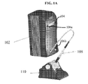
- FIG. 1A depicts an exemplary handheld soldering iron, according to some embodiments of the present invention.
- the handheld soldering iron includes a power supply unit 102 including a display 104, for example an LCD display, and various indicators 106, such as LED indicators 106a and 106b.
- the soldering iron further includes a hand piece 108 coupled to the power supply unit 102 and a (work) stand 11 that accommodates the hand piece 108.
- the hand piece 108 receives power from the power supply unit 102 and heats up a soldering tip to perform the soldering on a work piece.
- the soldering tip may include a temperature sensor to sense the tip temperature and transmit that data to the processor.
- the hand piece 108 may include various indicators such as one or more LEDs and/or a buzzer on it.
- the power supply unit 102 includes a microprocessor, memory, input/output circuitry and other necessary electronic circuitry to perform various processes.
- the microprocessor and the associated circuits identify what soldering cartridge is being used, validate the tip geometry, validate that the temperature and load are matched to ensure that the cartridge can produce sufficient energy to bring the load to solder melting point, detect liquidus temperature and then determine the thickness of the IMC, as described in more detail below.
- the soldering cartridge includes the soldering tip, associated wiring, magnetic shield, heater, shaft, connector(s), a non-volatile memory (NVM), one or more sensors, and a potentiometer to measure the impedance of the tip.
- the liquidus temperature is the temperature above which a material is completely liquid. Liquidus temperature is mostly used for impure substances (mixtures) such as glasses, alloys and rocks. Above the liquidus temperature the material is homogeneous and liquid at equilibrium. Below the liquidus temperature, more crystals are formed in the material after a sufficient time, depending on the material.
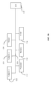
- FIG. 1B is an exemplary block diagram of a processor and associated components, according to some embodiments of the present invention.
- a processor 112 a memory 114 a non-volatile memory (NVM) 116 and an I/O interface 118 are coupled to a bus 120 to comprise the processor and associated circuitry of some embodiments of the present invention.
- the I/O interface 118 may be a wired interface and/or a wireless interface to components external to the soldering station.
- two cameras 122 and 124 are coupled to the processor and the memory via the bus 120 or the I/O interface 118 to capture images from a solder joint from different views.
- an optional temperature sensor 126 for sensing the temperature of the soldering tip may be coupled to the processor 112 and the memory 114 via the bus 120 or the I/O interface 118.
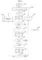
- FIG. 2 shows an exemplary process flow, according to some embodiments of the present invention.
- the cartridge being used is identified and the data related to the identified cartridge is retrieved from a non-volatile memory (NVM), such as an EEPROM.
- NVM non-volatile memory
- the NVM may be placed in the cartridge to store data related to the cartridge such as, part number, lot code, serial number, total usage, total point, tip mass/weight, tip configuration, authentication code (if any), thermal efficiency, thermal characteristic, and the like.
- This data may be retrieved periodically at the startup and during the operation.
- the data may also be received and transmitted via wire or wireless methods.
- block 206 checks the power level to determine whether any soldering action is being performed, within a period of time. If no soldering action to be performed yet, the process waits in block 206. For example, a timer can be set to a predetermined time and if no action happens within that time, the process waits. However, if a soldering action to be performed, the process proceeds to an optional block 208, where the indicators are reset.
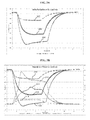
- FIG. 3A shows a graph for a change in temperature of a soldering tip over time, for three given load sizes.
- Graph 306 is for a large load size
- graph 304 is for a medium load size
- graph 302 shows a small load size.
- the heavier the load the higher temperature drop.
- the process is aborted since the power supply would be unable to recover fast enough to continue delivering power to the tip to maintain the temperature of the tip, within the required time to complete the soldering event (e.g., 8 seconds).
- the temperature drop may be detected by measuring the impedance of the tip and then determining the tip temperature by the equation (3) below.
- the impedance may be measured by turning off the power to the tip and measuring the voltage of the coil (in the cartridge). The impedance would then be the voltage of the coil times am Impedance Factor (K in Equation (3)), which would depend of the tip type.
- a temperature sensor may be placed in the tip to directly read the temperature drop and communicate it to the microprocessor.
- R imd R min + R max / 1 + k * e ⁇ - T
- R imd is the impedance value
- R min is a minimum value of the impedance
- R min is a maximum value of the impedance
- K is a weight factor
- T is delta temperature.
- FIG. 3B depicts a graph for a change in impedance of a soldering tip over time, for three given power levels that are delivered by the power supply unit to the soldering tip and three given temperatures of the soldering tip.
- Graph 318 is for a small power
- graph 312 is for a large power
- graph 314 shows a medium power.
- graph 310 is for a small temperature
- graph 316 is for medium temperature
- graph 320 is for a large temperature.
- the temperature drop may be detected by defining a thermal efficiency factor for each given tip geometry and heater material, as shown in Equation (4) below. If power draws higher than TE_factor, the system determines an abort in the process by, for example, turning on a red LED and/or a buzzer.
- TE_factor TipMass * TipStyle * HTR_factor * Const where, TipMass is the copper weight (mg), which is 0.65 for a "LongReach" tip, 1 for a "Regular” tip, and 1.72 for a "Power" tip. TipStyle refers to the distance from the tip of tip to the heater in the cartridge.
- a thermal efficiency check is performed to ensure that the tip geometry/temperature and the load are matched, based upon tip temperature drop within a predetermined time period, for example, the first 2-3 seconds.
- the thermal efficiency check checks the heat transfer and power recovery of the soldering station with respect to the tip and the load.
- Each tip type has its own thermal characteristic, which is a function of the tip temperature, mass, and configuration/style.
- their thermal efficiency factors (TEs) are stored in the NVM.
- the first period of time e.g., 2 - 3 seconds
- the power to the tip is measured and compared with the TE of the tip.
- the thermal efficiency check fails (210a), the process is aborted in block 226 and optionally one or more indicators, for example, a red LED and/or a buzzer, are turned on. If the thermal efficiency check passed (210b), the process proceeds to the optional block 212 where a "passing" indicator, such as a green LED and/or a beep, is turned on to let the operator know that the thermal efficiency check process has passed.
- a threshold value for example, 95% +/- 10% of TE
- the liquidus temperature is detected based on the following heat transfer equation.
- ⁇ T P * TR
- ⁇ T the tip temperature minus the load temperature
- P the power level
- TR the thermal resistant between the tip and the load that may be retrieved from the NVM.
- block 216 it is checked to see if the power is at a peak and declining. If not, the process is timed out (216a) and aborted in block 226. If the power is at a peak and declining, the process proceed to block 218 to turn on an indicator, for example, an LED and/or a beep sound. When the power is at a peak and declining, it means that the solder event is at liquidus state.
- the thickness of the IMC would be a function of time and temperature.
- the temperature is at melting point (e.g., at 220-240° C), it does not have a substantial impact on the thickness of the IMC. Accordingly, Equation (6) is based on only time and a fixed temperature.
- block 222 checks to see whether within a predetermine amount of time (cooling period), the determined thickness of the IMC is within a predetermined range, for example, 1um to 4 um. If it is, the processes proceeds to block 224, where the operator is informed. If the result of the test in block 222 is false, the process is timed out (222b) and aborted in block 226.
- the invention provides the operator with an indication of successful or potential non-successful joint formation, along with the ability to collect the intermetallic joint information, and the operational parameters for that particular joint for post processing. Indication can be accomplished via visual means, audible means, and/or vibration of the hand piece.
- a debug mode (block 228) is used, for example, by a process engineer to keep track of the steps involved during a solder event. To enter the debug mode, a user needs to turn the debug mode on.
- FIG. 4B illustrates a graph for the thickness for the IMC versus soldering time.
- X is the time
- Y is the IMC thickness.
- the constant numbers are derived from multiple experimentations.
- a break out of the IMC thickness happens at three different temperature ranges. Since the thickness of the IMC is a function of time and temperature, as temperature rises, the IMC grows larger, as a linear function. Depending on the application, any of these curves may be used to determine the weighing factor, K, in Equation (6). For example, for a soldering application with SAC305 tip, graph 404 is used.
- the embodiments of the present invention ensure a good bonding and electrical connection between two metals by calculating the intermetallic thickness and therefore prevent a bad joint in early stages.
- the invention provides instant feedback (by the indicators) to operators on joint quality and process issues and thus the operators have the ability to track information on joint quality for post analysis. The operators can change or select from a menu several parameters to meet certain application requirements.
- Curie temperature point
- SmartheatTM technology which is a self-regulated Curie temperature
- the Curie temperature or Curie point is the temperature where a material's permanent magnetism changes to induced magnetism, that is, the critical point where a material's intrinsic magnetic moments change direction.
- the invention also provides the capability to help the operators to identify whether they are using an improper tip/cartridge combination for a soldering event
- the invention uses at least two high resolution cameras to capture two or more 2D images, obtain a 3D image from those 2D images, use the 2D and 3D images to detect liquidus stage and then calculate the amount of solder filled through the via hole (barrel) for through hole components, or the amount solder spread out around the components for surface mount components.
- FIG. 5 is an exemplary process flow for liquidus detection and connection verification using images from a plurality of cameras, according to some embodiments of the present invention. At least two high resolution cameras are placed close to the soldering joint at two different locations to capture 2D images of the solder joint from two views, before and after the soldering event. The liquidus is detected from comparison of the 2D images. Then, in the case of through hole components, the volume of the through hole barrel (barrel) is determined from 3D images generated from the 2D images. In the case of surface mounted (SMT) components, the surface of the barrel on the PCB is determined from the 2D images.
- SMT surface mounted
- two images of the soldering area are captured by the two cameras, before the soldering event to generate two reference images, as depicted in FIG. 6A .
- a 3D reference image of the soldering area is generated from the two reference images, before the soldering event, by well know methods.
- the volume of the barrel V b for through hole and/or the surface area of the barrel S b for SMT component are determined from the 3D reference image to determine how much solder is need to fill the barrel or the surface area of the barrel.
- the surface of the barrel may also be determined from the 2D images, depending on the camera positions. Accordingly, the amount of solder needed to fill in the barrel or the surface of the barrel is determined, depending on the type of the component.
- two current images of the soldering area is captured, in block 508.
- the color value of each pixel in the 2D reference images is compared to color value of each corresponding pixel in the 2D current images, as the soldering event progresses, to detect any color changes of the pixels in the current images due to spread of the solder. Since the pixel value of the solder color is known, this the process can determine whether a pixel is a solder pixel, i.e., contains solder, as shown in FIG. 6B .
- the processes in blocks 508 ( FIG. 6C ) and 510 are repeated until all the pixels in the current images are determined to be pixels of the dispensed solder, that is, the liquidus is now detected, as depicted in FIG. 6D .
- the process in block 512 is timed out after a predetermined amount of time (e.g., 8 seconds), if not all the pixels in the current images are determined to be pixels of solder.
- a predetermined amount of time e.g. 8 seconds
- the last current image from each camera are processed to generate a 3D current image, in block 516.
- the volume of the dispensed solder V s is determined from the 3D current image, by one or more of Equations (7) to (9), in block 518.
- the calculated volume of the dispensed solder V s is compared to the determined amount of solder needed to fill in the barrel (i.e., V b ) or the surface area of the barrel (i.e., S b ) to determine how much of the dispensed solder is dissipated into the barrel or on the surface area of the barrel.
- This process (block 520) is repeated in block 522, until the dispensed solder has filed the barrel or the surface area of the barrel. That is, the volume of the visible dispensed solder has reached (V s Vb) or (V s S b ), within a predetermined tolerance range.
- the process in block 522 is timed out after a predetermined amount of time (e.g., 8 seconds).
- An indicator e.g., a LED and/or beep
- a good solder joint is formed, as shown in FIG. 7A .
- the calculation of the height and volume of the solder joint is performed based on the following equations.
- V lead ⁇ r lead 2 h
- V barrel ⁇ r barrel 2 h
- V required ⁇ h r barrel 2 - r lead 2
- V lead is the volume of component lead
- V barrel is the volume of through hole barrel
- V required is the volume of solder required to fill the barrel
- r lead is the (though hole) component lead radius
- r barrel is through hole barrel radius
- h is the board thickness, as shown in FIG. 7A .
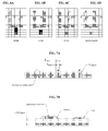
- FIG. 7A shows some exemplary solder joints, the image of which is captured by the two cameras, for through hole components, according to some embodiments of the present invention.
- FIG. 7B shows some exemplary solder joints, the image of which is captured by the two cameras, for surface mount components, according to some embodiments of the present invention.
- the invention compares the height of the entire load to a predetermined reference height (a desired height) to form a parabolic or linear shape. Once the identified shape area is equivalent to a predefined percentage of the load (barrel) surface area within a predefined tolerance, a good solder is formed for the surface mount component. As shown in FIG.
- the solder joint is formed on the side of the component as a parabolic shape.
- the solder joint is formed on the side of the component as a linear shape since the camera can only capture a linearly filled area due to the small size of the component.
Abstract
Description
- This Patent Application claims the benefit of the filing date of United States Provisional Patent Application Serial No.
62/033,037, filed on August 4, 2014 - The present invention relates generally to manufacturing, repair and rework of printed circuit boards (PCBs); and more particularly to a soldering iron with automatic soldering connection validation.
- With the greater variety of components used on printed circuit boards (PCBs), smaller passive components and larger ICs with finer ball pitch dimensions, the demands on high quality solder joints to aid PCB assembly (PCBA) fabrication and rework have increased. Faulty solder joint has cost companies billions of dollars over the years. Many processes have been developed to reduce failure rate for wave solder systems. However, for point to point handheld soldering and rework applications, companies are purely relying on operators' skills to produce good solder joints with quality electrical connections. Regardless of how much training is provided to the operators of the soldering iron, without guidance during a soldering activity, the operators may make and repeat mistakes due to the fact that there are many factors that impact heat transfer by the soldering iron for forming a solder joint with good electrical connection. These factors include solder tip temperature, geometry of the solder tip, oxidation of the solder, human behavior, and the like.
- In some embodiments, the present invention is a method performed by a handheld soldering iron station for a soldering joint connection validation, the handheld soldering iron station including a soldering cartridge having a soldering tip. The method includes: identifying a type of the soldering cartridge being used by the soldering iron station and obtaining information related to the identified cartridge; determining that a soldering event has started by measuring a power level delivered to the soldering tip, within a first predetermined time period; performing a preliminary validation by measuring a soldering tip temperature, after the soldering event has started; monitoring the power level delivered to the soldering tip to detect liquidus occurrence; determining a thickness of an intermetallic component (IMC) of the soldering joint as a function of soldering time and soldering tip temperature, after detect the liquidus occurrence; determining whether the thickness of the IMC is within a predetermined range, within a predetermined cooling time period; and indicating that a reliable soldering joint connection is formed, when the thickness of the IMC is within the predetermined range, within the predetermined cooling time period.
- In some embodiments, the present invention is a soldering iron station with automatic soldering joint connection validation including: a hand piece including a soldering cartridge having a soldering tip; a power supply for delivering power to the soldering tip; an indicator; and a processor including associated circuits for identifying a type of the soldering cartridge being used by the soldering iron station and obtaining information related to the identified cartridge; performing a preliminary validation by measuring a soldering tip temperature; monitoring the power level delivered to the soldering tip to detect liquidus occurrence; determining a thickness of an intermetallic component (IMC) of the soldering joint as a function of soldering time and soldering tip temperature, after detecting the liquidus occurrence; and determining whether the thickness of the IMC is within a predetermined range, within a predetermined cooling time period. The indicator indicates that a reliable soldering joint connection is formed, when the thickness of the IMC is within the predetermined range, within the predetermined cooling time period.
- In some embodiments, the present invention is a method performed by a handheld soldering iron station for a soldering joint connection validation, the handheld soldering iron station including two cameras for capturing respective images of the soldering joint from different views. The method includes: capturing a 2-dimensional (2D) reference image of the soldering joint by each of the cameras, before a soldering event starts; generating a 3-dimensional (3D) reference image of the soldering joint from the captured 2D reference images; determining an amount of solder needed to fill in a barrel of a hole for a through hole component, or to fill in a surface of a barrel of a hole for a surface mount component, from the 3D reference image; capturing a 2D current image of the soldering joint by each of the cameras, after the soldering event starts; comparing a value of each pixel in each of the 2D current images to corresponding pixel values in the 2D reference images, respectively to detect any color changes of the pixels in the 2D current images due to spread of a dispensed solder, as the soldering event progresses; repeating capturing a 2D current image and comparing a value of each pixel, until all the pixels in the 2D current images are determined to be pixels of the dispensed solder to detect an occurrence of a liquidus of the dispensed solder; after detection of the occurrence of the liquidus, generating a 3D current image of the soldering joint from the last captured 2D reference image from each camera; determining volume of the dispensed solder after occurrence of the liquidus from the 3D current image; comparing the volume of the dispensed solder to the determined amount of solder needed to fill in the barrel or the surface area of the barrel to determine how much of the dispensed solder is dissipated into the barrel or on the surface area of the barrel; repeating the comparing of the volume of the dispensed solder until the dispensed solder has filed the barrel or the surface area of the barrel, within a predetermined tolerance; and activating an indicator to indicate a good connection, when the dispensed solder has filed the barrel or the surface area of the barrel within the predetermined tolerance.
- In some embodiments, the present invention is a soldering iron station with automatic validation of connection of a soldering joint comprising: a hand piece including a soldering tip; a power supply for delivering power to the soldering tip; two cameras positioned at different locations, each for capturing a 2-dimensional (2D) image of the soldering joint; an indicator; and a processor including associated circuits for validation of the connection of the soldering joint. Each of the cameras captures a 2-dimensional (2D) reference image of the soldering joint by each of the cameras, before a soldering event starts; the processor generates a 3-dimensional (3D) reference image of the soldering joint from the captured 2D reference images and determines an amount of solder needed to fill in a barrel of a hole for a through hole component, or to fill in a surface of a barrel of a hole for a surface mount component, from the 3D reference image; each of the cameras captures a 2D current image of the soldering joint, after the soldering event starts, the processor compares a value of each pixel in each of the 2D current images to corresponding pixel values in the 2D reference images, respectively to detect any color changes of the pixels in the 2D current images due to spread of a dispensed solder, as the soldering event progresses, each of the cameras repeats capturing a 2D current image and the processor repeats comparing a value of each pixel, until all the pixels in the 2D current images are determined to be pixels of the dispensed solder to detect an occurrence of a liquidus of the dispensed solder, after detection of the occurrence of the liquidus, the processor generates a 3D current image of the soldering joint from the last captured 2D reference image from each camera, determines volume of the dispensed solder after occurrence of the liquidus from the 3D current image, compares the volume of the dispensed solder to the determined amount of solder needed to fill in the barrel or the surface area of the barrel to determine how much of the dispensed solder is dissipated into the barrel or on the surface area of the barrel, and repeats the comparing of the volume of the dispensed solder until the dispensed solder has filed the barrel or the surface area of the barrel within a predetermined tolerance. The soldering station further includes an indicator to indicate a good connection, when the dispensed solder has filed the barrel or the surface area of the barrel within the predetermined tolerance.
-
-
FIG. 1A depicts an exemplary handheld soldering iron, according to some embodiments of the present invention. -
FIG. 1B is an exemplary block diagram of a processor and associated components, according to some embodiments of the present invention. -
FIG. 2 shows an exemplary process flow, according to some embodiments of the present invention. -
FIG. 3A shows a graph for a change in temperature of a soldering tip over time, for three given load sizes, according to some embodiments of the present invention. -
FIG. 3B depicts a graph for a change in impedance of a soldering tip over time, for three given power levels and three given temperatures, according to some embodiments of the present invention. -
FIG. 4A illustrates a graph for the thickness of the IMC versus time, according to some embodiments of the present invention. -
FIG. 4B illustrates a graph for the thickness for the IMC versus soldering time, according to some embodiments of the present invention. -
FIG. 5 is an exemplary process flow for liquidus detection and connection verification using images from a plurality of cameras, according to some embodiments of the present invention. -
FIGs. 6A - 6D show various images used for detection of liquidus, according to some embodiments of the present invention. -
FIG. 7A shows some exemplary solder joints for through hole components, according to some embodiments of the present invention. -
FIG. 7B depicts some exemplary solder joints for surface mount components, according to some embodiments of the present invention. - In some embodiments, the present invention is a soldering iron with automatic soldering connection validation. The soldering iron includes a processor, such as a microprocessor or controller, memory, input/output circuitry and other necessary electronic circuitry to perform the soldering connection validation.
- In some embodiments, the processor receive various characteristics of the soldering joint and soldering iron and performs a process of calculating the intermetallic IMC thickness of solder and PCB substrate to ensure a good solder joint is formed during a soldering event. Once a good electrical connection for the solder joint is confirmed, an audio or LED indicator in the soldering iron, for example, in a hand piece, informs the operator of the formation of the good solder joint. Typically, a good solder joint formed by SAC solder and copper substrate PCB is when the intermetallic thickness is within 1um - 4um. Accordingly, if the operator uses, for example, SAC305 (96.5% Sn, 3% Ag, 0.5% Cu) solder wire with copper substrate PCB, intermetallic thickness Cu6Sn5 is calculated by some embodiments of the present invention and the operator is notified once the intermetallic thickness of the intermetallic compound (IMC) reaches 1um - 4 um, during the soldering.
- The chemical reaction between the copper substrate and the soldering iron can be shown as:
3Cu + Sn -> Cu3Sn (phase 1) (1)
2Cu3Sn + 3Sn -> Cu6Sn5 (phase 2 - IMC 1um - 4 um) (2).
-
Phase 1 of the chemical reaction is temporary (transient) and therefore is not used for determination of the quality of the solder joint. - In some embodiments, the microprocessor (or the controller) may be placed in the power supply, in the hand piece, or a stand of the soldering system. Communication with external devices, such as a local computer, a remote server, a printer and the like, may be performed at the work stand by wired and/or wireless connections, using the known wireless interfaces.
-
FIG. 1A depicts an exemplary handheld soldering iron, according to some embodiments of the present invention. As shown, the handheld soldering iron includes apower supply unit 102 including adisplay 104, for example an LCD display, and various indicators 106, such asLED indicators hand piece 108 coupled to thepower supply unit 102 and a (work) stand 11 that accommodates thehand piece 108. Thehand piece 108 receives power from thepower supply unit 102 and heats up a soldering tip to perform the soldering on a work piece. In some embodiments, the soldering tip may include a temperature sensor to sense the tip temperature and transmit that data to the processor. - The
hand piece 108 may include various indicators such as one or more LEDs and/or a buzzer on it. In some embodiment, thepower supply unit 102 includes a microprocessor, memory, input/output circuitry and other necessary electronic circuitry to perform various processes. - In some embodiments, the microprocessor and the associated circuits identify what soldering cartridge is being used, validate the tip geometry, validate that the temperature and load are matched to ensure that the cartridge can produce sufficient energy to bring the load to solder melting point, detect liquidus temperature and then determine the thickness of the IMC, as described in more detail below. In some embodiments, the soldering cartridge includes the soldering tip, associated wiring, magnetic shield, heater, shaft, connector(s), a non-volatile memory (NVM), one or more sensors, and a potentiometer to measure the impedance of the tip. The liquidus temperature is the temperature above which a material is completely liquid. Liquidus temperature is mostly used for impure substances (mixtures) such as glasses, alloys and rocks. Above the liquidus temperature the material is homogeneous and liquid at equilibrium. Below the liquidus temperature, more crystals are formed in the material after a sufficient time, depending on the material.
-
FIG. 1B is an exemplary block diagram of a processor and associated components, according to some embodiments of the present invention. As illustrated, aprocessor 112, a memory 114 a non-volatile memory (NVM) 116 and an I/O interface 118 are coupled to abus 120 to comprise the processor and associated circuitry of some embodiments of the present invention. The I/O interface 118 may be a wired interface and/or a wireless interface to components external to the soldering station. Optionally, twocameras bus 120 or the I/O interface 118 to capture images from a solder joint from different views. Additionally, anoptional temperature sensor 126 for sensing the temperature of the soldering tip may be coupled to theprocessor 112 and thememory 114 via thebus 120 or the I/O interface 118. -
FIG. 2 shows an exemplary process flow, according to some embodiments of the present invention. As shown inblock 202, The process for validating all the connections joint between the component and the PCB substrate starts. Inblock 204, the cartridge being used is identified and the data related to the identified cartridge is retrieved from a non-volatile memory (NVM), such as an EEPROM. In some embodiments, the NVM may be placed in the cartridge to store data related to the cartridge such as, part number, lot code, serial number, total usage, total point, tip mass/weight, tip configuration, authentication code (if any), thermal efficiency, thermal characteristic, and the like. This data may be retrieved periodically at the startup and during the operation. In some embodiments, the data may also be received and transmitted via wire or wireless methods. - In
block 206, checks the power level to determine whether any soldering action is being performed, within a period of time. If no soldering action to be performed yet, the process waits inblock 206. For example, a timer can be set to a predetermined time and if no action happens within that time, the process waits. However, if a soldering action to be performed, the process proceeds to anoptional block 208, where the indicators are reset. -
FIG. 3A shows a graph for a change in temperature of a soldering tip over time, for three given load sizes.Graph 306 is for a large load size,graph 304 is for a medium load size andgraph 302 shows a small load size. As illustrated inFIG. 3A , for a given tip, the heavier the load, the higher temperature drop. In some embodiments, if the tip temperature drop is greater than a predetermined value, for example, 25° C, the process is aborted since the power supply would be unable to recover fast enough to continue delivering power to the tip to maintain the temperature of the tip, within the required time to complete the soldering event (e.g., 8 seconds). - In some embodiments, the temperature drop may be detected by measuring the impedance of the tip and then determining the tip temperature by the equation (3) below. The impedance may be measured by turning off the power to the tip and measuring the voltage of the coil (in the cartridge). The impedance would then be the voltage of the coil times am Impedance Factor (K in Equation (3)), which would depend of the tip type. In some embodiments, a temperature sensor may be placed in the tip to directly read the temperature drop and communicate it to the microprocessor.

- Where, Rimd is the impedance value, Rmin is a minimum value of the impedance, Rmin is a maximum value of the impedance, K is a weight factor and T is delta temperature.
-
FIG. 3B depicts a graph for a change in impedance of a soldering tip over time, for three given power levels that are delivered by the power supply unit to the soldering tip and three given temperatures of the soldering tip.Graph 318 is for a small power,graph 312 is for a large power andgraph 314 shows a medium power. Moreover,graph 310 is for a small temperature,graph 316 is for medium temperature andgraph 320 is for a large temperature. - In some embodiments, the temperature drop may be detected by defining a thermal efficiency factor for each given tip geometry and heater material, as shown in Equation (4) below. If power draws higher than TE_factor, the system determines an abort in the process by, for example, turning on a red LED and/or a buzzer.

where, TipMass is the copper weight (mg), which is 0.65 for a "LongReach" tip, 1 for a "Regular" tip, and 1.72 for a "Power" tip. TipStyle refers to the distance from the tip of tip to the heater in the cartridge. For example, TipStyle is 20 mm for a "LongReach" tip, 10 mm for a "Regular" tip, and 5 mm for a "Power" tip. HTR_factor is the heater temperature times a factor (e.g., 0.01), which changes based on the type of the heater. Const = 4.651 * 10-3 for all types of heaters.. For example, the HTR_factor may be 800F * 0.01 = 8; 700F* 0.01 = 7; 600F* 0.01 = 6; or 500F* 0.01 = 5 for various heater types. - Referring back to
FIG. 2 , inblock 210, a thermal efficiency check is performed to ensure that the tip geometry/temperature and the load are matched, based upon tip temperature drop within a predetermined time period, for example, the first 2-3 seconds. In some embodiments, the thermal efficiency check checks the heat transfer and power recovery of the soldering station with respect to the tip and the load. Each tip type has its own thermal characteristic, which is a function of the tip temperature, mass, and configuration/style. For various tip types, their thermal efficiency factors (TEs) are stored in the NVM. During the first period of time (e.g., 2 - 3 seconds), the power to the tip is measured and compared with the TE of the tip. If the measured power is greater than a threshold value, for example, 95% +/- 10% of TE, it means that the tip is too small or the load is too large, become they require a lot of power. In this case, the thermal efficiency check fails (210a), the process is aborted inblock 226 and optionally one or more indicators, for example, a red LED and/or a buzzer, are turned on. If the thermal efficiency check passed (210b), the process proceeds to theoptional block 212 where a "passing" indicator, such as a green LED and/or a beep, is turned on to let the operator know that the thermal efficiency check process has passed. - In
block 214, the liquidus temperature is detected based on the following heat transfer equation.
where, ΔT is the tip temperature minus the load temperature, P is the power level, and TR is the thermal resistant between the tip and the load that may be retrieved from the NVM. - Since load temperature continues to increase until it reaches equilibrium, ΔT decreases throughout the soldering action. Also, power increases when the soldering event first starts. Therefore, TR will be decreasing, as shown below. Once liquidus occurs, TR is stabilized and thus the power P now starts decreasing, as shown below. Accordingly, to detect liquidus temperature, the change state in the power delivered to the soldering tip is observed.


- In
block 216, it is checked to see if the power is at a peak and declining. If not, the process is timed out (216a) and aborted inblock 226. If the power is at a peak and declining, the process proceed to block 218 to turn on an indicator, for example, an LED and/or a beep sound. When the power is at a peak and declining, it means that the solder event is at liquidus state. - In
block 220, the thickness of the IMC is determined by the following equation.
where k is a weighing factor and t is solder interval time @100ms. - Generally, the thickness of the IMC would be a function of time and temperature. When the temperature is at melting point (e.g., at 220-240° C), it does not have a substantial impact on the thickness of the IMC. Accordingly, Equation (6) is based on only time and a fixed temperature.
-
FIG. 4A illustrates a graph for the thickness of the IMC versus time, for k = 0.2173, which is obtain by experimentation, using many soldering joint and IMC thickness measurement. As depicted inFIG. 4A , the IMC thickness increases over time. - Referring back to
FIG. 2 , block 222 checks to see whether within a predetermine amount of time (cooling period), the determined thickness of the IMC is within a predetermined range, for example, 1um to 4 um. If it is, the processes proceeds to block 224, where the operator is informed. If the result of the test inblock 222 is false, the process is timed out (222b) and aborted inblock 226. - In some embodiments, the invention provides the operator with an indication of successful or potential non-successful joint formation, along with the ability to collect the intermetallic joint information, and the operational parameters for that particular joint for post processing. Indication can be accomplished via visual means, audible means, and/or vibration of the hand piece.
- A debug mode (block 228) is used, for example, by a process engineer to keep track of the steps involved during a solder event. To enter the debug mode, a user needs to turn the debug mode on.
-
FIG. 4B illustrates a graph for the thickness for the IMC versus soldering time. As depicted,graph 402 is for a temperature of 300 ° C with Y = 0.176X + 1.242,graph 404 is for a temperature of 275 ° C with Y = 0.044X + 1.019, andgraph 404 is for a temperature of 220 ° C with Y = 0.049X + 0.297, where X is the time and Y is the IMC thickness. The constant numbers are derived from multiple experimentations. As shown, a break out of the IMC thickness happens at three different temperature ranges. Since the thickness of the IMC is a function of time and temperature, as temperature rises, the IMC grows larger, as a linear function. Depending on the application, any of these curves may be used to determine the weighing factor, K, in Equation (6). For example, for a soldering application with SAC305 tip,graph 404 is used. - This way, the embodiments of the present invention ensure a good bonding and electrical connection between two metals by calculating the intermetallic thickness and therefore prevent a bad joint in early stages. Moreover, the invention provides instant feedback (by the indicators) to operators on joint quality and process issues and thus the operators have the ability to track information on joint quality for post analysis. The operators can change or select from a menu several parameters to meet certain application requirements.
- In some embodiments, when a Curie temperature (point)/Smartheat™ technology, which is a self-regulated Curie temperature, is utilized, there is no requirement for calibration of the system at customer site. The Curie temperature or Curie point, is the temperature where a material's permanent magnetism changes to induced magnetism, that is, the critical point where a material's intrinsic magnetic moments change direction. The invention also provides the capability to help the operators to identify whether they are using an improper tip/cartridge combination for a soldering event
- In some embodiments, the invention uses at least two high resolution cameras to capture two or more 2D images, obtain a 3D image from those 2D images, use the 2D and 3D images to detect liquidus stage and then calculate the amount of solder filled through the via hole (barrel) for through hole components, or the amount solder spread out around the components for surface mount components.
-
FIG. 5 is an exemplary process flow for liquidus detection and connection verification using images from a plurality of cameras, according to some embodiments of the present invention. At least two high resolution cameras are placed close to the soldering joint at two different locations to capture 2D images of the solder joint from two views, before and after the soldering event. The liquidus is detected from comparison of the 2D images. Then, in the case of through hole components, the volume of the through hole barrel (barrel) is determined from 3D images generated from the 2D images. In the case of surface mounted (SMT) components, the surface of the barrel on the PCB is determined from the 2D images. As shown inblock 502, two images of the soldering area (joint) are captured by the two cameras, before the soldering event to generate two reference images, as depicted inFIG. 6A . Inblock 504, a 3D reference image of the soldering area is generated from the two reference images, before the soldering event, by well know methods. - In
block 506, the volume of the barrel Vb for through hole and/or the surface area of the barrel Sb for SMT component are determined from the 3D reference image to determine how much solder is need to fill the barrel or the surface area of the barrel. The surface of the barrel may also be determined from the 2D images, depending on the camera positions. Accordingly, the amount of solder needed to fill in the barrel or the surface of the barrel is determined, depending on the type of the component. Immediately after the soldering event is started, two current images of the soldering area is captured, inblock 508. Inblock 510, the color value of each pixel in the 2D reference images is compared to color value of each corresponding pixel in the 2D current images, as the soldering event progresses, to detect any color changes of the pixels in the current images due to spread of the solder. Since the pixel value of the solder color is known, this the process can determine whether a pixel is a solder pixel, i.e., contains solder, as shown inFIG. 6B . - In
block 512, the processes in blocks 508 (FIG. 6C ) and 510 are repeated until all the pixels in the current images are determined to be pixels of the dispensed solder, that is, the liquidus is now detected, as depicted inFIG. 6D . The process inblock 512 is timed out after a predetermined amount of time (e.g., 8 seconds), if not all the pixels in the current images are determined to be pixels of solder. When all the pixels in the last two current images are determined to be pixels of the dispensed solder (within a tolerance range), the liquidus is detected, inblock 514. - After the detection of the liquidus, the last current image from each camera are processed to generate a 3D current image, in
block 516. Then, the volume of the dispensed solder Vs is determined from the 3D current image, by one or more of Equations (7) to (9), inblock 518. Inblock 520, the calculated volume of the dispensed solder Vs is compared to the determined amount of solder needed to fill in the barrel (i.e., Vb) or the surface area of the barrel (i.e., Sb) to determine how much of the dispensed solder is dissipated into the barrel or on the surface area of the barrel. This process (block 520) is repeated inblock 522, until the dispensed solder has filed the barrel or the surface area of the barrel. That is, the volume of the visible dispensed solder has reached (Vs Vb) or (Vs Sb), within a predetermined tolerance range. The process inblock 522 is timed out after a predetermined amount of time (e.g., 8 seconds). An indicator (e.g., a LED and/or beep) is then turn on to notify the operator that the connection is now formed by filling all of the barrel or the surface of the barrel with the dispensed solder. - In other words, in the case of a through hole component, when the calculated volume reduces to a predetermined amount that is needed to fill the barrel and within a pre-defined tolerance for through hole component, a good solder joint is formed, as shown in
FIG. 7A . In some embodiments, the calculation of the height and volume of the solder joint is performed based on the following equations.


Where, Vlead is the volume of component lead; Vbarrel is the volume of through hole barrel; Vrequired is the volume of solder required to fill the barrel, rlead is the (though hole) component lead radius; rbarrel is through hole barrel radius; and h is the board thickness, as shown inFIG. 7A . -
FIG. 7A shows some exemplary solder joints, the image of which is captured by the two cameras, for through hole components, according to some embodiments of the present invention..FIG. 7B shows some exemplary solder joints, the image of which is captured by the two cameras, for surface mount components, according to some embodiments of the present invention. In this case, the invention compares the height of the entire load to a predetermined reference height (a desired height) to form a parabolic or linear shape. Once the identified shape area is equivalent to a predefined percentage of the load (barrel) surface area within a predefined tolerance, a good solder is formed for the surface mount component. As shown inFIG. 7B , for a larger surface mount component, the solder joint is formed on the side of the component as a parabolic shape. However, for a smaller surface mount component, the solder joint is formed on the side of the component as a linear shape since the camera can only capture a linearly filled area due to the small size of the component. - It will be recognized by those skilled in the art that various modifications may be made to the illustrated and other embodiments of the invention described above, without departing from the broad inventive step thereof. It will be understood therefore that the invention is not limited to the particular embodiments or arrangements disclosed, but is rather intended to cover any changes, adaptations or modifications which are within the scope and spirit of the invention as defined by the appended claims.
Claims (15)
- A method performed by a handheld soldering iron station for a soldering joint connection validation, the handheld soldering iron station including a soldering cartridge having a soldering tip, the method comprising:identifying a type of the soldering cartridge being used by the soldering iron station and obtaining information related to the identified cartridge;determining that a soldering event has started by measuring a power level delivered to the soldering tip, within a first predetermined time period;performing a preliminary validation by measuring a soldering tip temperature, after the soldering event has started;monitoring the power level delivered to the soldering tip to detect liquidus occurrence;determining a thickness of an intermetallic component (IMC) of the soldering joint as a function of soldering time and soldering tip temperature, after detect the liquidus occurrence;determining whether the thickness of the IMC is within a predetermined range, within a predetermined cooling time period; andindicating that a reliable soldering joint connection is formed, when the thickness of the IMC is within the predetermined range, within the predetermined cooling time period.
- The method of claim 1, wherein identifying a type of the soldering cartridge being used and obtaining information related to the identified cartridge comprises retrieving data from a memory within the soldering iron station, or from a memory remote from the soldering iron station.
- The method of claim 1 or 2, wherein measuring a soldering tip temperature comprises measuring an impedance of the soldering tip and determining the soldering tip temperature as a function of the measured impedance.
- The method according to one of the claims 1 to 3, wherein measuring a soldering tip temperature comprises defining a thermal efficiency factor for a geometry of the soldering tip and a heater material and determining the soldering tip temperature as a function of the thermal efficiency and the powered delivered to the soldering tip.
- The method according to one of the claims 1 to 4, wherein the liquidus occurrence is detected when the monitored power is declining from a peak, and
wherein in particular the predetermined range of the thickness of the IMC is 1um - 4 um. - The method of claim according to one of the claims 1 to 5, further comprising performing a thermal efficiency check and aborting the method when the thermal efficiency check fails.
- A soldering iron station with automatic soldering joint connection validation comprising:a hand piece including a soldering cartridge having a soldering tip;a power supply for delivering power to the soldering tip;an indicator; anda processor including associated circuits for identifying a type of the soldering cartridge being used by the soldering iron station and obtaining information related to the identified cartridge; performing a preliminary validation by measuring a soldering tip temperature; monitoring the power level delivered to the soldering tip to detect liquidus occurrence; determining a thickness of an intermetallic component (IMC) of the soldering joint as a function of soldering time and soldering tip temperature, after detecting the liquidus occurrence; and determining whether the thickness of the IMC is within a predetermined range, within a predetermined cooling time period, whereinthe indicator indicates that a reliable soldering joint connection is formed, when the thickness of the IMC is within the predetermined range, within the predetermined cooling time period.
- The soldering iron station of claim 7, wherein the soldering iron station further includes a non-volatile memory (NVM) for storing data related to the cartridge, and wherein the processor identifies the type of the soldering cartridge being used and obtains information related to the identified cartridge by retrieving data from the NVM,
wherein in particular data related to the cartridge stored in the NVM includes one or more of part number, lot code, serial number, total usage, total point, tip mass/weight, tip configuration, authentication code, thermal efficiency, and thermal characteristic. - The soldering iron station of claim 7 or 8, further comprising a temperature sensor for measuring the soldering tip temperature.
- The soldering iron station according to one of the claims 7 to 9, wherein the processor detects the liquidus occurrence when the monitored power is declining from a peak.
- A method performed by a handheld soldering iron station for a soldering joint connection validation, the handheld soldering iron station including two cameras for capturing respective images of the soldering joint from different views, the method comprising:capturing a 2-dimensional (2D) reference image of the soldering joint by each of the cameras, before a soldering event starts;generating a 3-dimensional (3D) reference image of the soldering joint from the captured 2D reference images;determining an amount of solder needed to fill in a barrel of a hole for a through hole component, or to fill in a surface of a barrel of a hole for a surface mount component, from the 3D reference image;capturing a 2D current image of the soldering joint by each of the cameras, after the soldering event starts;comparing a value of each pixel in each of the 2D current images to corresponding pixel values in the 2D reference images, respectively to detect any color changes of the pixels in the 2D current images due to spread of a dispensed solder, as the soldering event progresses;repeating capturing a 2D current image and comparing a value of each pixel, until all the pixels in the 2D current images are determined to be pixels of the dispensed solder to detect an occurrence of a liquidus of the dispensed solder;after detection of the occurrence of the liquidus, generating a 3D current image of the soldering joint from the last captured 2D reference image from each camera;determining volume of the dispensed solder after occurrence of the liquidus from the 3D current image;comparing the volume of the dispensed solder to the determined amount of solder needed to fill in the barrel or the surface area of the barrel to determine how much of the dispensed solder is dissipated into the barrel or on the surface area of the barrel;repeating the comparing of the volume of the dispensed solder until the dispensed solder has filed the barrel or the surface area of the barrel, within a predetermined tolerance; andactivating an indicator to indicate a good connection, when the dispensed solder has filed the barrel or the surface area of the barrel within the predetermined tolerance.
- The method of claim 11, wherein comparing a value of each pixel in each of the 2D current images comprises comparing a color value of each pixel in each of the 2D current images to corresponding pixel color values in the 2D reference images, respectively in relation to a known color pixel value of solder, wherein in particular detection of the occurrence of the liquidus of the dispensed solder is determined when all of the pixel color values in the last two 2D current images are equal to the known color pixel value of solder, within a tolerance range.
- The method of claim 11 or 12, further comprising aborting the method when within a predetermined time period, not all the pixels in the 2D current images are determined to be pixels of the dispensed solder, and/or further comprising aborting the method when within a predetermined time period, the dispensed solder has not filed the barrel or the surface area of the barrel within said predetermined tolerance.
- A soldering iron station with automatic validation of connection of a soldering joint comprising:a hand piece including a soldering tip;a power supply for delivering power to the soldering tip;two cameras positioned at different locations, each for capturing a 2-dimensional (2D) image of the soldering joint;an indicator; anda processor including associated circuits for validation of the connection of the soldering joint, whereineach of the cameras captures a 2-dimensional (2D) reference image of the soldering joint by each of the cameras, before a soldering event starts,the processor generates a 3-dimensional (3D) reference image of the soldering joint from the captured 2D reference images and determines an amount of solder needed to fill in a barrel of a hole for a through hole component, or to fill in a surface of a barrel of a hole for a surface mount component, from the 3D reference image,each of the cameras captures a 2D current image of the soldering joint, after the soldering event starts,the processor compares a value of each pixel in each of the 2D current images to corresponding pixel values in the 2D reference images, respectively to detect any color changes of the pixels in the 2D current images due to spread of a dispensed solder, as the soldering event progresses,each of the cameras repeats capturing a 2D current image and the processor repeats comparing a value of each pixel, until all the pixels in the 2D current images are determined to be pixels of the dispensed solder to detect an occurrence of a liquidus of the dispensed solder,after detection of the occurrence of the liquidus, the processor generates a 3D current image of the soldering joint from the last captured 2D reference image from each camera, determines volume of the dispensed solder after occurrence of the liquidus from the 3D current image, compares the volume of the dispensed solder to the determined amount of solder needed to fill in the barrel or the surface area of the barrel to determine how much of the dispensed solder is dissipated into the barrel or on the surface area of the barrel, and repeats the comparing of the volume of the dispensed solder until the dispensed solder has filed the barrel or the surface area of the barrel within a predetermined tolerance; andan indicator to indicate a good connection, when the dispensed solder has filed the barrel or the surface area of the barrel within the predetermined tolerance.
- The soldering iron station of claim 14, wherein the processor compares a color value of each pixel in each of the 2D current images to corresponding pixel color values in the 2D reference images, respectively in relation to a known color pixel value of solder,
wherein in particular the processor detects the occurrence of the liquidus of the dispensed solder when all of the pixel color values in the last two 2D current images are equal to the known color pixel value of solder, within a tolerance range.
Applications Claiming Priority (2)
| Application Number | Priority Date | Filing Date | Title |
|---|---|---|---|
| US201462033037P | 2014-08-04 | 2014-08-04 | |
| US14/794,678 US9516762B2 (en) | 2014-08-04 | 2015-07-08 | Soldering iron with automatic soldering connection validation |
Publications (3)
| Publication Number | Publication Date |
|---|---|
| EP3000550A2 true EP3000550A2 (en) | 2016-03-30 |
| EP3000550A3 EP3000550A3 (en) | 2016-07-27 |
| EP3000550B1 EP3000550B1 (en) | 2019-01-16 |
Family
ID=55179080
Family Applications (1)
| Application Number | Title | Priority Date | Filing Date |
|---|---|---|---|
| EP15179757.8A Active EP3000550B1 (en) | 2014-08-04 | 2015-08-04 | Soldering iron with automatic soldering connection validation |
Country Status (10)
| Country | Link |
|---|---|
| US (2) | US9516762B2 (en) |
| EP (1) | EP3000550B1 (en) |
| JP (2) | JP6166315B2 (en) |
| KR (2) | KR20160016709A (en) |
| CN (3) | CN107322121B (en) |
| AU (2) | AU2015205882B2 (en) |
| BR (1) | BR102015018596A2 (en) |
| CA (1) | CA2898031A1 (en) |
| MX (1) | MX346045B (en) |
| TW (1) | TW201609299A (en) |
Families Citing this family (26)
| Publication number | Priority date | Publication date | Assignee | Title |
|---|---|---|---|---|
| GB2507719A (en) * | 2012-09-25 | 2014-05-14 | Pillarhouse Int Ltd | Method and apparatus for improving selective soldering |
| US10716220B2 (en) | 2014-08-04 | 2020-07-14 | Ok International, Inc. | Variable temperature controlled soldering iron |
| US9516762B2 (en) * | 2014-08-04 | 2016-12-06 | Ok International Inc. | Soldering iron with automatic soldering connection validation |
| US10688578B2 (en) | 2014-08-04 | 2020-06-23 | OK International, Inc | Variable temperature controlled soldering iron |
| US9327361B2 (en) * | 2014-08-04 | 2016-05-03 | Ok International Inc. | Intelligent soldering cartridge for automatic soldering connection validation |
| US10777005B2 (en) * | 2014-12-15 | 2020-09-15 | Autodesk, Inc. | Smart tools and workspaces for do-it-yourself tasks |
| CA2915654C (en) * | 2015-07-08 | 2018-05-01 | Delaware Capital Formation, Inc. | An intelligent soldering cartridge for automatic soldering connection validation |
| CN107283016A (en) * | 2016-04-11 | 2017-10-24 | Ok国际公司 | The controlled flatiron of variable temperature |
| EP3532232A4 (en) | 2016-10-26 | 2020-07-15 | Milwaukee Electric Tool Corporation | Soldering tool |
| JP6550082B2 (en) * | 2017-01-17 | 2019-07-24 | 白光株式会社 | Soldering equipment |
| CN107087348B (en) * | 2017-06-26 | 2019-04-09 | 潍坊路加精工有限公司 | A kind of attaching method and device of circuit board |
| WO2019031484A1 (en) * | 2017-08-10 | 2019-02-14 | 白光株式会社 | Soldering iron control device, cartridge, and soldering iron management system |
| KR102299768B1 (en) | 2017-09-11 | 2021-09-07 | 주식회사 엘지화학 | Method for laser welding of different metals with optimization of welding condition by using intermetallic compound analysis |
| USD852596S1 (en) | 2017-10-26 | 2019-07-02 | Milwaukee Electric Tool Corporation | Soldering tool |
| CN110297013A (en) * | 2018-03-23 | 2019-10-01 | 台达电子工业股份有限公司 | Solder method |
| US10780515B2 (en) * | 2018-04-26 | 2020-09-22 | Raytheon Technologies Corporation | Auto-adaptive braze dispensing systems and methods |
| US10974335B2 (en) * | 2018-07-10 | 2021-04-13 | Hakko Corporation | Composite soldering, de-soldering station load detection |
| JP6517412B1 (en) * | 2018-07-12 | 2019-05-22 | 白光株式会社 | Soldering iron controller |
| US10751823B2 (en) * | 2018-09-25 | 2020-08-25 | Ok International, Inc. | Smart soldering iron tip and method of authenticating same |
| US10751822B2 (en) * | 2018-09-25 | 2020-08-25 | Ok International, Inc. | Smart soldering iron tip and method of authenticating same |
| CN111745249A (en) * | 2019-03-26 | 2020-10-09 | Ok国际公司 | Variable temperature controlled soldering iron |
| EP3791986A1 (en) * | 2019-08-05 | 2021-03-17 | OK International, Inc. | Variable temperature controlled soldering iron |
| CN111243229A (en) * | 2019-12-31 | 2020-06-05 | 浙江大学 | Old people falling risk assessment method and system |
| TWI760870B (en) * | 2020-09-29 | 2022-04-11 | 台達電子工業股份有限公司 | Soldering process monitoring system and method |
| USD1004653S1 (en) * | 2023-03-14 | 2023-11-14 | Meihua Li | Soldering station |
| USD998666S1 (en) * | 2023-04-17 | 2023-09-12 | Guangzhou e-Design Intelligent Technology Co., Ltd. | Cordless soldering station |
Family Cites Families (37)
| Publication number | Priority date | Publication date | Assignee | Title |
|---|---|---|---|---|
| US4418268A (en) | 1981-01-22 | 1983-11-29 | Munshaw Harold A | Soldering iron holder with ready indicator and safety shutoff |
| US4801069A (en) | 1987-03-30 | 1989-01-31 | Westinghouse Electric Corp. | Method and apparatus for solder deposition |
| US4792078A (en) | 1987-06-11 | 1988-12-20 | Kiyohachi Takahashi | Device for controlling concentration and temperature of flux |
| US5223689A (en) | 1989-06-13 | 1993-06-29 | Metcal, Inc. | Profiles to insure proper heating function |
| CA2018561C (en) | 1989-06-13 | 1994-08-30 | Mark J. Cowell | Solder joint system |
| DE4143545C2 (en) | 1990-11-29 | 2002-09-05 | Matsushita Electric Ind Co Ltd | Testing external quality of objects, esp. components on PCB |
| US5495093A (en) | 1993-02-05 | 1996-02-27 | Edsyn, Inc. | Soldering apparatus processor having temperature selection, calibration and heating control of tip |
| JPH0894330A (en) * | 1994-09-22 | 1996-04-12 | Aisin Seiki Co Ltd | Non-contact appearance inspection device and non-contact capacity inspection device |
| JPH10137929A (en) * | 1996-11-12 | 1998-05-26 | Hitachi Ltd | Method and device for brazing |
| JP2984659B1 (en) | 1998-07-31 | 1999-11-29 | 米沢日本電気株式会社 | Soldering equipment and solder supply instruction method |
| US5928536A (en) | 1998-09-21 | 1999-07-27 | Lee; Cheng-Liang | Electric soldering iron with heating energy regulating control means |
| US6946623B2 (en) | 2000-09-15 | 2005-09-20 | Powerpulse Technologies, L.P. | Appliance for liquefying solder with variable duty cycle and method of implementing |
| US6563087B1 (en) | 2001-11-14 | 2003-05-13 | Hakko Corporation | Automated soldering system |
| JP2003181632A (en) * | 2001-12-11 | 2003-07-02 | Matsushita Electric Ind Co Ltd | Method and device for soldering |
| US6580050B1 (en) | 2002-01-16 | 2003-06-17 | Pace, Incorporated | Soldering station with built-in self-calibration function |
| JP3878023B2 (en) * | 2002-02-01 | 2007-02-07 | シーケーディ株式会社 | 3D measuring device |
| US7044354B2 (en) | 2003-04-01 | 2006-05-16 | Hakko Corporation | Soldering system with indicator lights displaying system status |
| CN100489508C (en) * | 2004-07-21 | 2009-05-20 | 欧姆龙株式会社 | Methods of and apparatus for inspecting substrate |
| SG121898A1 (en) * | 2004-10-06 | 2006-05-26 | Generic Power Pte Ltd | System for 2-D and 3-D vision inspection |
| US8733620B2 (en) | 2005-12-08 | 2014-05-27 | Intel Corporation | Solder deposition and thermal processing of thin-die thermal interface material |
| US7681776B2 (en) | 2006-08-01 | 2010-03-23 | Raytheon Company | Methods and apparatus for efficiently generating profiles for circuit board work/rework |
| JP3962782B1 (en) * | 2006-08-11 | 2007-08-22 | 国立大学法人 岡山大学 | Soldering inspection method, solder bonding method, and solder bonding apparatus |
| JP4140860B1 (en) | 2007-06-18 | 2008-08-27 | 国立大学法人 岡山大学 | Soldering method and soldering apparatus |
| JP5426081B2 (en) | 2007-06-20 | 2014-02-26 | スタンレー電気株式会社 | Substrate bonding method and semiconductor device |
| JP2009092485A (en) * | 2007-10-06 | 2009-04-30 | Djtech Co Ltd | Print solder inspection device |
| JP2009166062A (en) * | 2008-01-12 | 2009-07-30 | Engineer Inc | Temperature control device of soldering iron |
| JP2009257857A (en) | 2008-04-15 | 2009-11-05 | Yamatake Corp | Melting temperature determination apparatus |
| JP2010029888A (en) | 2008-07-25 | 2010-02-12 | Okayama Univ | Soldering inspection method and soldering equipment |
| CN101358836B (en) * | 2008-09-28 | 2010-09-29 | 西安理工大学 | Method for recognizing weld spot central position based on computer vision |
| US8274011B2 (en) | 2009-01-24 | 2012-09-25 | Hakko Corporation | Soldering device and method of making same |
| KR101121994B1 (en) | 2010-02-02 | 2012-03-09 | 주식회사 고영테크놀러지 | Method of generating inspection program |
| JP5328707B2 (en) | 2010-03-29 | 2013-10-30 | 三菱電機株式会社 | Quality control method and quality control apparatus for solder joints |
| KR101184875B1 (en) * | 2011-06-28 | 2012-09-20 | 삼성전기주식회사 | Electric joint structure, and method for preparing the same |
| CN103398660B (en) * | 2013-08-05 | 2015-12-09 | 河北工业大学 | For obtaining the structured light vision sensor parameter calibration method of weld bead height information |
| US9327361B2 (en) * | 2014-08-04 | 2016-05-03 | Ok International Inc. | Intelligent soldering cartridge for automatic soldering connection validation |
| US9516762B2 (en) * | 2014-08-04 | 2016-12-06 | Ok International Inc. | Soldering iron with automatic soldering connection validation |
| JP6396117B2 (en) * | 2014-08-19 | 2018-09-26 | 五洋建設株式会社 | Concrete surface quality evaluation apparatus and concrete surface quality evaluation method |
-
2015
- 2015-07-08 US US14/794,678 patent/US9516762B2/en not_active Expired - Fee Related
- 2015-07-21 CA CA2898031A patent/CA2898031A1/en not_active Abandoned
- 2015-07-22 AU AU2015205882A patent/AU2015205882B2/en not_active Ceased
- 2015-07-28 MX MX2015009716A patent/MX346045B/en active IP Right Grant
- 2015-07-29 TW TW104124518A patent/TW201609299A/en unknown
- 2015-08-03 BR BR102015018596A patent/BR102015018596A2/en not_active IP Right Cessation
- 2015-08-03 KR KR1020150109543A patent/KR20160016709A/en active IP Right Grant
- 2015-08-04 CN CN201710600269.7A patent/CN107322121B/en active Active
- 2015-08-04 CN CN201520579509.6U patent/CN205096679U/en not_active Withdrawn - After Issue
- 2015-08-04 CN CN201510471647.7A patent/CN105328292B/en active Active
- 2015-08-04 EP EP15179757.8A patent/EP3000550B1/en active Active
- 2015-08-04 JP JP2015154143A patent/JP6166315B2/en active Active
-
2016
- 2016-11-01 US US15/340,384 patent/US9629295B2/en active Active
- 2016-12-06 AU AU2016269424A patent/AU2016269424A1/en not_active Abandoned
- 2016-12-19 JP JP2016245299A patent/JP2017070999A/en active Pending
-
2017
- 2017-06-14 KR KR1020170074906A patent/KR20170073559A/en active IP Right Grant
Non-Patent Citations (1)
| Title |
|---|
| None |
Also Published As
| Publication number | Publication date |
|---|---|
| AU2016269424A1 (en) | 2016-12-22 |
| CA2898031A1 (en) | 2016-02-04 |
| AU2015205882A1 (en) | 2016-02-18 |
| KR20160016709A (en) | 2016-02-15 |
| CN107322121B (en) | 2019-08-27 |
| MX346045B (en) | 2017-03-03 |
| US20170049017A1 (en) | 2017-02-16 |
| TW201609299A (en) | 2016-03-16 |
| US20160031044A1 (en) | 2016-02-04 |
| AU2015205882B2 (en) | 2017-01-12 |
| KR20170073559A (en) | 2017-06-28 |
| MX2015009716A (en) | 2016-04-20 |
| JP6166315B2 (en) | 2017-07-19 |
| CN205096679U (en) | 2016-03-23 |
| US9516762B2 (en) | 2016-12-06 |
| BR102015018596A2 (en) | 2016-05-24 |
| CN105328292A (en) | 2016-02-17 |
| CN107322121A (en) | 2017-11-07 |
| JP2017070999A (en) | 2017-04-13 |
| EP3000550B1 (en) | 2019-01-16 |
| EP3000550A3 (en) | 2016-07-27 |
| JP2016034665A (en) | 2016-03-17 |
| CN105328292B (en) | 2017-12-08 |
| US9629295B2 (en) | 2017-04-18 |
Similar Documents
| Publication | Publication Date | Title |
|---|---|---|
| US9629295B2 (en) | Soldering station with automatic soldering connection validation | |
| US9629257B2 (en) | Intelligent soldering cartridge for automatic soldering connection validation | |
| EP3115142B1 (en) | An intelligent soldering cartridge for automatic soldering connection validation | |
| US10688578B2 (en) | Variable temperature controlled soldering iron | |
| US10645817B1 (en) | Variable temperature controlled soldering iron | |
| US20170173719A1 (en) | Variable temperature controlled soldering iron | |
| EP3791986A1 (en) | Variable temperature controlled soldering iron |
Legal Events
| Date | Code | Title | Description |
|---|---|---|---|
| PUAI | Public reference made under article 153(3) epc to a published international application that has entered the european phase |
Free format text: ORIGINAL CODE: 0009012 |
|
| AK | Designated contracting states |
Kind code of ref document: A2 Designated state(s): AL AT BE BG CH CY CZ DE DK EE ES FI FR GB GR HR HU IE IS IT LI LT LU LV MC MK MT NL NO PL PT RO RS SE SI SK SM TR |
|
| AX | Request for extension of the european patent |
Extension state: BA ME |
|
| RAP1 | Party data changed (applicant data changed or rights of an application transferred) |
Owner name: OK INTERNATIONAL INC |
|
| PUAL | Search report despatched |
Free format text: ORIGINAL CODE: 0009013 |
|
| AK | Designated contracting states |
Kind code of ref document: A3 Designated state(s): AL AT BE BG CH CY CZ DE DK EE ES FI FR GB GR HR HU IE IS IT LI LT LU LV MC MK MT NL NO PL PT RO RS SE SI SK SM TR |
|
| AX | Request for extension of the european patent |
Extension state: BA ME |
|
| RIC1 | Information provided on ipc code assigned before grant |
Ipc: B23K 3/03 20060101AFI20160622BHEP Ipc: G01B 11/00 20060101ALI20160622BHEP Ipc: B23K 31/12 20060101ALI20160622BHEP Ipc: B23K 3/08 20060101ALI20160622BHEP Ipc: G06T 15/08 20110101ALI20160622BHEP Ipc: B23K 1/00 20060101ALI20160622BHEP |
|
| STAA | Information on the status of an ep patent application or granted ep patent |
Free format text: STATUS: REQUEST FOR EXAMINATION WAS MADE |
|
| RAP1 | Party data changed (applicant data changed or rights of an application transferred) |
Owner name: OK INTERNATIONAL, INC. |
|
| 17P | Request for examination filed |
Effective date: 20161026 |
|
| RBV | Designated contracting states (corrected) |
Designated state(s): AL AT BE BG CH CY CZ DE DK EE ES FI FR GB GR HR HU IE IS IT LI LT LU LV MC MK MT NL NO PL PT RO RS SE SI SK SM TR |
|
| GRAP | Despatch of communication of intention to grant a patent |
Free format text: ORIGINAL CODE: EPIDOSNIGR1 |
|
| STAA | Information on the status of an ep patent application or granted ep patent |
Free format text: STATUS: GRANT OF PATENT IS INTENDED |
|
| INTG | Intention to grant announced |
Effective date: 20180807 |
|
| GRAS | Grant fee paid |
Free format text: ORIGINAL CODE: EPIDOSNIGR3 |
|
| GRAA | (expected) grant |
Free format text: ORIGINAL CODE: 0009210 |
|
| STAA | Information on the status of an ep patent application or granted ep patent |
Free format text: STATUS: THE PATENT HAS BEEN GRANTED |
|
| AK | Designated contracting states |
Kind code of ref document: B1 Designated state(s): AL AT BE BG CH CY CZ DE DK EE ES FI FR GB GR HR HU IE IS IT LI LT LU LV MC MK MT NL NO PL PT RO RS SE SI SK SM TR |
|
| REG | Reference to a national code |
Ref country code: GB Ref legal event code: FG4D |
|
| REG | Reference to a national code |
Ref country code: CH Ref legal event code: EP |
|
| REG | Reference to a national code |
Ref country code: IE Ref legal event code: FG4D |
|
| REG | Reference to a national code |
Ref country code: DE Ref legal event code: R096 Ref document number: 602015023517 Country of ref document: DE |
|
| REG | Reference to a national code |
Ref country code: AT Ref legal event code: REF Ref document number: 1089347 Country of ref document: AT Kind code of ref document: T Effective date: 20190215 |
|
| REG | Reference to a national code |
Ref country code: NL Ref legal event code: MP Effective date: 20190116 |
|
| REG | Reference to a national code |
Ref country code: LT Ref legal event code: MG4D |
|
| PG25 | Lapsed in a contracting state [announced via postgrant information from national office to epo] |
Ref country code: NL Free format text: LAPSE BECAUSE OF FAILURE TO SUBMIT A TRANSLATION OF THE DESCRIPTION OR TO PAY THE FEE WITHIN THE PRESCRIBED TIME-LIMIT Effective date: 20190116 |
|
| REG | Reference to a national code |
Ref country code: AT Ref legal event code: MK05 Ref document number: 1089347 Country of ref document: AT Kind code of ref document: T Effective date: 20190116 |
|
| PG25 | Lapsed in a contracting state [announced via postgrant information from national office to epo] |
Ref country code: PL Free format text: LAPSE BECAUSE OF FAILURE TO SUBMIT A TRANSLATION OF THE DESCRIPTION OR TO PAY THE FEE WITHIN THE PRESCRIBED TIME-LIMIT Effective date: 20190116 Ref country code: LT Free format text: LAPSE BECAUSE OF FAILURE TO SUBMIT A TRANSLATION OF THE DESCRIPTION OR TO PAY THE FEE WITHIN THE PRESCRIBED TIME-LIMIT Effective date: 20190116 Ref country code: FI Free format text: LAPSE BECAUSE OF FAILURE TO SUBMIT A TRANSLATION OF THE DESCRIPTION OR TO PAY THE FEE WITHIN THE PRESCRIBED TIME-LIMIT Effective date: 20190116 Ref country code: NO Free format text: LAPSE BECAUSE OF FAILURE TO SUBMIT A TRANSLATION OF THE DESCRIPTION OR TO PAY THE FEE WITHIN THE PRESCRIBED TIME-LIMIT Effective date: 20190416 Ref country code: SE Free format text: LAPSE BECAUSE OF FAILURE TO SUBMIT A TRANSLATION OF THE DESCRIPTION OR TO PAY THE FEE WITHIN THE PRESCRIBED TIME-LIMIT Effective date: 20190116 Ref country code: PT Free format text: LAPSE BECAUSE OF FAILURE TO SUBMIT A TRANSLATION OF THE DESCRIPTION OR TO PAY THE FEE WITHIN THE PRESCRIBED TIME-LIMIT Effective date: 20190516 Ref country code: ES Free format text: LAPSE BECAUSE OF FAILURE TO SUBMIT A TRANSLATION OF THE DESCRIPTION OR TO PAY THE FEE WITHIN THE PRESCRIBED TIME-LIMIT Effective date: 20190116 |
|
| PG25 | Lapsed in a contracting state [announced via postgrant information from national office to epo] |
Ref country code: BG Free format text: LAPSE BECAUSE OF FAILURE TO SUBMIT A TRANSLATION OF THE DESCRIPTION OR TO PAY THE FEE WITHIN THE PRESCRIBED TIME-LIMIT Effective date: 20190416 Ref country code: HR Free format text: LAPSE BECAUSE OF FAILURE TO SUBMIT A TRANSLATION OF THE DESCRIPTION OR TO PAY THE FEE WITHIN THE PRESCRIBED TIME-LIMIT Effective date: 20190116 Ref country code: GR Free format text: LAPSE BECAUSE OF FAILURE TO SUBMIT A TRANSLATION OF THE DESCRIPTION OR TO PAY THE FEE WITHIN THE PRESCRIBED TIME-LIMIT Effective date: 20190417 Ref country code: LV Free format text: LAPSE BECAUSE OF FAILURE TO SUBMIT A TRANSLATION OF THE DESCRIPTION OR TO PAY THE FEE WITHIN THE PRESCRIBED TIME-LIMIT Effective date: 20190116 Ref country code: IS Free format text: LAPSE BECAUSE OF FAILURE TO SUBMIT A TRANSLATION OF THE DESCRIPTION OR TO PAY THE FEE WITHIN THE PRESCRIBED TIME-LIMIT Effective date: 20190516 Ref country code: RS Free format text: LAPSE BECAUSE OF FAILURE TO SUBMIT A TRANSLATION OF THE DESCRIPTION OR TO PAY THE FEE WITHIN THE PRESCRIBED TIME-LIMIT Effective date: 20190116 |
|
| REG | Reference to a national code |
Ref country code: DE Ref legal event code: R097 Ref document number: 602015023517 Country of ref document: DE |
|
| PG25 | Lapsed in a contracting state [announced via postgrant information from national office to epo] |
Ref country code: AL Free format text: LAPSE BECAUSE OF FAILURE TO SUBMIT A TRANSLATION OF THE DESCRIPTION OR TO PAY THE FEE WITHIN THE PRESCRIBED TIME-LIMIT Effective date: 20190116 Ref country code: DK Free format text: LAPSE BECAUSE OF FAILURE TO SUBMIT A TRANSLATION OF THE DESCRIPTION OR TO PAY THE FEE WITHIN THE PRESCRIBED TIME-LIMIT Effective date: 20190116 Ref country code: IT Free format text: LAPSE BECAUSE OF FAILURE TO SUBMIT A TRANSLATION OF THE DESCRIPTION OR TO PAY THE FEE WITHIN THE PRESCRIBED TIME-LIMIT Effective date: 20190116 Ref country code: AT Free format text: LAPSE BECAUSE OF FAILURE TO SUBMIT A TRANSLATION OF THE DESCRIPTION OR TO PAY THE FEE WITHIN THE PRESCRIBED TIME-LIMIT Effective date: 20190116 Ref country code: EE Free format text: LAPSE BECAUSE OF FAILURE TO SUBMIT A TRANSLATION OF THE DESCRIPTION OR TO PAY THE FEE WITHIN THE PRESCRIBED TIME-LIMIT Effective date: 20190116 Ref country code: SK Free format text: LAPSE BECAUSE OF FAILURE TO SUBMIT A TRANSLATION OF THE DESCRIPTION OR TO PAY THE FEE WITHIN THE PRESCRIBED TIME-LIMIT Effective date: 20190116 Ref country code: RO Free format text: LAPSE BECAUSE OF FAILURE TO SUBMIT A TRANSLATION OF THE DESCRIPTION OR TO PAY THE FEE WITHIN THE PRESCRIBED TIME-LIMIT Effective date: 20190116 Ref country code: CZ Free format text: LAPSE BECAUSE OF FAILURE TO SUBMIT A TRANSLATION OF THE DESCRIPTION OR TO PAY THE FEE WITHIN THE PRESCRIBED TIME-LIMIT Effective date: 20190116 |
|
| PLBE | No opposition filed within time limit |
Free format text: ORIGINAL CODE: 0009261 |
|
| STAA | Information on the status of an ep patent application or granted ep patent |
Free format text: STATUS: NO OPPOSITION FILED WITHIN TIME LIMIT |
|
| PG25 | Lapsed in a contracting state [announced via postgrant information from national office to epo] |
Ref country code: SM Free format text: LAPSE BECAUSE OF FAILURE TO SUBMIT A TRANSLATION OF THE DESCRIPTION OR TO PAY THE FEE WITHIN THE PRESCRIBED TIME-LIMIT Effective date: 20190116 |
|
| 26N | No opposition filed |
Effective date: 20191017 |
|
| PG25 | Lapsed in a contracting state [announced via postgrant information from national office to epo] |
Ref country code: SI Free format text: LAPSE BECAUSE OF FAILURE TO SUBMIT A TRANSLATION OF THE DESCRIPTION OR TO PAY THE FEE WITHIN THE PRESCRIBED TIME-LIMIT Effective date: 20190116 |
|
| PG25 | Lapsed in a contracting state [announced via postgrant information from national office to epo] |
Ref country code: TR Free format text: LAPSE BECAUSE OF FAILURE TO SUBMIT A TRANSLATION OF THE DESCRIPTION OR TO PAY THE FEE WITHIN THE PRESCRIBED TIME-LIMIT Effective date: 20190116 |
|
| PG25 | Lapsed in a contracting state [announced via postgrant information from national office to epo] |
Ref country code: MC Free format text: LAPSE BECAUSE OF FAILURE TO SUBMIT A TRANSLATION OF THE DESCRIPTION OR TO PAY THE FEE WITHIN THE PRESCRIBED TIME-LIMIT Effective date: 20190116 Ref country code: LI Free format text: LAPSE BECAUSE OF NON-PAYMENT OF DUE FEES Effective date: 20190831 Ref country code: CH Free format text: LAPSE BECAUSE OF NON-PAYMENT OF DUE FEES Effective date: 20190831 Ref country code: LU Free format text: LAPSE BECAUSE OF NON-PAYMENT OF DUE FEES Effective date: 20190804 |
|
| REG | Reference to a national code |
Ref country code: BE Ref legal event code: MM Effective date: 20190831 |
|
| PG25 | Lapsed in a contracting state [announced via postgrant information from national office to epo] |
Ref country code: IE Free format text: LAPSE BECAUSE OF NON-PAYMENT OF DUE FEES Effective date: 20190804 |
|
| PG25 | Lapsed in a contracting state [announced via postgrant information from national office to epo] |
Ref country code: BE Free format text: LAPSE BECAUSE OF NON-PAYMENT OF DUE FEES Effective date: 20190831 |
|
| PG25 | Lapsed in a contracting state [announced via postgrant information from national office to epo] |
Ref country code: CY Free format text: LAPSE BECAUSE OF FAILURE TO SUBMIT A TRANSLATION OF THE DESCRIPTION OR TO PAY THE FEE WITHIN THE PRESCRIBED TIME-LIMIT Effective date: 20190116 |
|
| PG25 | Lapsed in a contracting state [announced via postgrant information from national office to epo] |
Ref country code: MT Free format text: LAPSE BECAUSE OF FAILURE TO SUBMIT A TRANSLATION OF THE DESCRIPTION OR TO PAY THE FEE WITHIN THE PRESCRIBED TIME-LIMIT Effective date: 20190116 Ref country code: HU Free format text: LAPSE BECAUSE OF FAILURE TO SUBMIT A TRANSLATION OF THE DESCRIPTION OR TO PAY THE FEE WITHIN THE PRESCRIBED TIME-LIMIT; INVALID AB INITIO Effective date: 20150804 |
|
| PG25 | Lapsed in a contracting state [announced via postgrant information from national office to epo] |
Ref country code: MK Free format text: LAPSE BECAUSE OF FAILURE TO SUBMIT A TRANSLATION OF THE DESCRIPTION OR TO PAY THE FEE WITHIN THE PRESCRIBED TIME-LIMIT Effective date: 20190116 |
|
| P01 | Opt-out of the competence of the unified patent court (upc) registered |
Effective date: 20230526 |
|
| PGFP | Annual fee paid to national office [announced via postgrant information from national office to epo] |
Ref country code: FR Payment date: 20230620 Year of fee payment: 9 |
|
| PGFP | Annual fee paid to national office [announced via postgrant information from national office to epo] |
Ref country code: GB Payment date: 20230615 Year of fee payment: 9 |
|
| PGFP | Annual fee paid to national office [announced via postgrant information from national office to epo] |
Ref country code: DE Payment date: 20230613 Year of fee payment: 9 |