EP2996233A1 - Semiconductor device - Google Patents
Semiconductor device Download PDFInfo
- Publication number
- EP2996233A1 EP2996233A1 EP15178167.1A EP15178167A EP2996233A1 EP 2996233 A1 EP2996233 A1 EP 2996233A1 EP 15178167 A EP15178167 A EP 15178167A EP 2996233 A1 EP2996233 A1 EP 2996233A1
- Authority
- EP
- European Patent Office
- Prior art keywords
- igbt
- line
- igbt chips
- semiconductor device
- parallel
- Prior art date
- Legal status (The legal status is an assumption and is not a legal conclusion. Google has not performed a legal analysis and makes no representation as to the accuracy of the status listed.)
- Granted
Links
Images





Classifications
-
- H—ELECTRICITY
- H03—ELECTRONIC CIRCUITRY
- H03K—PULSE TECHNIQUE
- H03K17/00—Electronic switching or gating, i.e. not by contact-making and –breaking
- H03K17/51—Electronic switching or gating, i.e. not by contact-making and –breaking characterised by the components used
- H03K17/56—Electronic switching or gating, i.e. not by contact-making and –breaking characterised by the components used by the use, as active elements, of semiconductor devices
- H03K17/567—Circuits characterised by the use of more than one type of semiconductor device, e.g. BIMOS, composite devices such as IGBT
-
- H—ELECTRICITY
- H02—GENERATION; CONVERSION OR DISTRIBUTION OF ELECTRIC POWER
- H02M—APPARATUS FOR CONVERSION BETWEEN AC AND AC, BETWEEN AC AND DC, OR BETWEEN DC AND DC, AND FOR USE WITH MAINS OR SIMILAR POWER SUPPLY SYSTEMS; CONVERSION OF DC OR AC INPUT POWER INTO SURGE OUTPUT POWER; CONTROL OR REGULATION THEREOF
- H02M1/00—Details of apparatus for conversion
- H02M1/08—Circuits specially adapted for the generation of control voltages for semiconductor devices incorporated in static converters
- H02M1/088—Circuits specially adapted for the generation of control voltages for semiconductor devices incorporated in static converters for the simultaneous control of series or parallel connected semiconductor devices
-
- H—ELECTRICITY
- H02—GENERATION; CONVERSION OR DISTRIBUTION OF ELECTRIC POWER
- H02M—APPARATUS FOR CONVERSION BETWEEN AC AND AC, BETWEEN AC AND DC, OR BETWEEN DC AND DC, AND FOR USE WITH MAINS OR SIMILAR POWER SUPPLY SYSTEMS; CONVERSION OF DC OR AC INPUT POWER INTO SURGE OUTPUT POWER; CONTROL OR REGULATION THEREOF
- H02M7/00—Conversion of AC power input into DC power output; Conversion of DC power input into AC power output
- H02M7/42—Conversion of DC power input into AC power output without possibility of reversal
- H02M7/44—Conversion of DC power input into AC power output without possibility of reversal by static converters
- H02M7/48—Conversion of DC power input into AC power output without possibility of reversal by static converters using discharge tubes with control electrode or semiconductor devices with control electrode
- H02M7/483—Converters with outputs that each can have more than two voltages levels
- H02M7/487—Neutral point clamped inverters
-
- H—ELECTRICITY
- H02—GENERATION; CONVERSION OR DISTRIBUTION OF ELECTRIC POWER
- H02M—APPARATUS FOR CONVERSION BETWEEN AC AND AC, BETWEEN AC AND DC, OR BETWEEN DC AND DC, AND FOR USE WITH MAINS OR SIMILAR POWER SUPPLY SYSTEMS; CONVERSION OF DC OR AC INPUT POWER INTO SURGE OUTPUT POWER; CONTROL OR REGULATION THEREOF
- H02M7/00—Conversion of AC power input into DC power output; Conversion of DC power input into AC power output
- H02M7/42—Conversion of DC power input into AC power output without possibility of reversal
- H02M7/44—Conversion of DC power input into AC power output without possibility of reversal by static converters
- H02M7/48—Conversion of DC power input into AC power output without possibility of reversal by static converters using discharge tubes with control electrode or semiconductor devices with control electrode
- H02M7/497—Conversion of DC power input into AC power output without possibility of reversal by static converters using discharge tubes with control electrode or semiconductor devices with control electrode sinusoidal output voltages being obtained by combination of several voltages being out of phase
-
- H—ELECTRICITY
- H10—SEMICONDUCTOR DEVICES; ELECTRIC SOLID-STATE DEVICES NOT OTHERWISE PROVIDED FOR
- H10W—GENERIC PACKAGES, INTERCONNECTIONS, CONNECTORS OR OTHER CONSTRUCTIONAL DETAILS OF DEVICES COVERED BY CLASS H10
- H10W72/00—Interconnections or connectors in packages
- H10W72/071—Connecting or disconnecting
- H10W72/075—Connecting or disconnecting of bond wires
- H10W72/07551—Connecting or disconnecting of bond wires characterised by changes in properties of the bond wires during the connecting
- H10W72/07552—Connecting or disconnecting of bond wires characterised by changes in properties of the bond wires during the connecting changes in structures or sizes
-
- H—ELECTRICITY
- H10—SEMICONDUCTOR DEVICES; ELECTRIC SOLID-STATE DEVICES NOT OTHERWISE PROVIDED FOR
- H10W—GENERIC PACKAGES, INTERCONNECTIONS, CONNECTORS OR OTHER CONSTRUCTIONAL DETAILS OF DEVICES COVERED BY CLASS H10
- H10W72/00—Interconnections or connectors in packages
- H10W72/50—Bond wires
- H10W72/521—Structures or relative sizes of bond wires
- H10W72/527—Multiple bond wires having different sizes
-
- H—ELECTRICITY
- H10—SEMICONDUCTOR DEVICES; ELECTRIC SOLID-STATE DEVICES NOT OTHERWISE PROVIDED FOR
- H10W—GENERIC PACKAGES, INTERCONNECTIONS, CONNECTORS OR OTHER CONSTRUCTIONAL DETAILS OF DEVICES COVERED BY CLASS H10
- H10W72/00—Interconnections or connectors in packages
- H10W72/50—Bond wires
- H10W72/531—Shapes of wire connectors
- H10W72/5363—Shapes of wire connectors the connected ends being wedge-shaped
-
- H—ELECTRICITY
- H10—SEMICONDUCTOR DEVICES; ELECTRIC SOLID-STATE DEVICES NOT OTHERWISE PROVIDED FOR
- H10W—GENERIC PACKAGES, INTERCONNECTIONS, CONNECTORS OR OTHER CONSTRUCTIONAL DETAILS OF DEVICES COVERED BY CLASS H10
- H10W72/00—Interconnections or connectors in packages
- H10W72/50—Bond wires
- H10W72/541—Dispositions of bond wires
- H10W72/547—Dispositions of multiple bond wires
- H10W72/5473—Dispositions of multiple bond wires multiple bond wires connected to a common bond pad
-
- H—ELECTRICITY
- H10—SEMICONDUCTOR DEVICES; ELECTRIC SOLID-STATE DEVICES NOT OTHERWISE PROVIDED FOR
- H10W—GENERIC PACKAGES, INTERCONNECTIONS, CONNECTORS OR OTHER CONSTRUCTIONAL DETAILS OF DEVICES COVERED BY CLASS H10
- H10W72/00—Interconnections or connectors in packages
- H10W72/90—Bond pads, in general
- H10W72/921—Structures or relative sizes of bond pads
- H10W72/926—Multiple bond pads having different sizes
Definitions
- the present invention relates to a semiconductor device, in particular to a semiconductor device that is a power conversion module accommodating a plurality of switching elements connected in series in a package and connecting plural sets of the plurality of series-connected switching elements in parallel to increase current carrying capacity of the semiconductor device.
- IGBTs insulated gate bipolar transistors
- a semiconductor device having a multilevel inverter circuit is known to meet the requirements for down-sizing and high performance.
- the multilevel inverter circuit outputs multi-levels of voltages in combination of plurality of IGBTs, and is disclosed in Patent Document 1, for example.
- FIG. 7 is a circuit diagram of a one phase, three-level inverter circuit of a general construction using switching elements of IGBTs.
- FIG. 8 is a circuit diagram of a first example of a three-level inverter circuit with increased current carrying capacity
- FIG. 9 is a circuit diagram of a second example of a three-level inverter circuit with increased current carrying capacity.
- the three-level inverter circuit of FIG. 7 comprises: four IGBTs 101, 102, 103, and 104; four free-wheeling diodes 105, 106, 107, and 108; and two clamping diodes 109 and 110.
- the IGBTs 101, 102, 103, and 104 having respective antiparallel-connected free-wheeling diodes 105, 106, 107, and 108 are each composed of a discrete module.
- the IGBTs 101, 102, 103, and 104 are connected in series and the middle node is connected to an output terminal 111.
- a node between the IGBT 101 and the IGBT 102 composing an upper arm of the inverter circuit is connected to a clamping diode 109.
- a node between the IGBT 103 and the IGBT 104 composing a lower arm of the inverter circuit is connected to a clamping diode 110.
- the clamping diodes 109 and 110 also compose a module.
- the emitter terminal of the IGBT 104 is connected to the negative terminal potential N of a power supply.
- the collector terminal of the IGBT 101 is connected to the positive terminal potential P of the power supply.
- the node between the clamping diodes 109 and 110 is connected to the middle potential M of the power supply.
- a voltage having three-levels of potential in each of the positive and negative sides is delivered from the output terminal 111 by ON/OFF-controlling the IGBTs 101, 102, 103, and 104.
- Each of the IGBTs 101, 102, 103, and 104 is a module having a current carrying capacity corresponding to the rated output of the inverter circuit.
- the upper arm of the inverter circuit is composed of a series-connect two sets of modules, one set being composed of a module of an IGBT 101a and a module of an IGBT 101b connected in parallel, and another set being composed of a module of an IGBT 102a and a module of an IGBT 102b connected in parallel.
- the lower arm of the inverter circuit is composed of a series-connected two sets of modules, one set being composed of a module of an IGBT 103a and a module of an IGBT 103b connected in parallel, and another set being composed of a module of an IGBT 104a and a module of an IGBT 104b connected in parallel.
- the modules are prepared separately and then assembled together, leading to complicated wiring.
- drive circuits have to be prepared individually.
- FIG. 9 shows another example of inverter circuit.
- This inverter circuit is not composed of a combination of a plurality of modules but formed of a single module that is composed of a plurality of chips combined together.
- the inverter circuit of FIG. 9 is composed of two sets of circuits, each set being composed of series-connected chips and being similar to the inverter circuit of FIG. 7 ,
- the upper arm of the inverter circuit comprises series-connected IGBT chips 121 and 122 and series connected IGBT chips 131 and 132 that are connected in parallel to the series-connected IGBT chips 121 and 122.
- the lower arm of the inverter circuit comprises series-connected IGBT chips 123 and 124 and series connected IGBT chips 133 and 134 that are connected in parallel to the series-connected IGBT chips 123 and 124.
- the corresponding IGBT chips 121 and 131 have a common gate terminal 141 and a common auxiliary emitter terminal 151; and the corresponding IGBT chips 122 and 132 have a common gate terminal 142 and a common auxiliary emitter terminal 152.
- the corresponding IGBT chips 123 and 133 have a common gate terminal 143 and a common auxiliary emitter terminal 153; and the corresponding IGBT chips 124 and 134 have a common gate terminal 144 and a common auxiliary emitter terminal 154.
- the auxiliary emitter terminal 151 is connected to the emitter of the IGBT chip 121 and further to the emitter of the IGBT chip 131 through an auxiliary emitter line 161.
- the auxiliary emitter terminal 152 is connected to the emitter of the IGBT chip 122 and further to the emitter of the IGBT chip 132 through an auxiliary emitter line 162.
- the auxiliary emitter terminal 153 is connected to the emitter of the IGBT chip 123 and further to the emitter of the IGBT chip 133 through an auxiliary emitter line 163.
- the auxiliary emitter terminal 154 is connected to the emitter of the IGBT chip 124 and further to the emitter of the IGBT chip 134 through an auxiliary emitter line 164.
- the node between the IGBT chips 122 and 123 is connected to the node between the IGBT chips 132 and 133 through an output line 171, and the node between the IGBT chips 132 and 133 is connected to an output terminal 111 through an output line 172.
- the clamping diode 125 is connected to the node between the IGBT chips 121 and 122, and the clamping diode 126 is connected to the node between the IGBT chips 123 and 124.
- the clamping diode 135 is connected to the node between the IGBT chips 131 and 132, and the clamping diode 136 is connected to the node between the IGBT chips 133 and 134.
- a voltage with three-levels of potential in each of positive and negative sides is delivered from the output terminal 111 by ON/OFF-controlling the IGBT chips 121 and 131, the IGBT chips 122 and 132, the IGBT chips 123 and 133, and the IGBT chips 124 and 134.
- the four IGBT chips 121, 122, 131, and 132 of the upper ram in FIG. 9 have not necessarily equivalent characteristics, but for example ON resistances are different in the ON operation.
- the IGBT chips 121 and 132 exhibit relatively low ON resistance and the IGBT chips 122 and 131 exhibit relatively high ON resistance.
- the IGBT chip 121 with lower ON resistance tends to carry larger current than the IGBT chip 131 with higher ON resistance; and the IGBT chip 132 with lower ON resistance tends to carry larger current than the IGBT chip 122 with higher ON resistance.
- the current supplied from the positive potential terminal P flows in larger amount through the path of IGBT chip 121, the auxiliary emitter line 161, and the IGBT chip 132 to the output terminal 111.
- the current flowing in the auxiliary emitter line 161 generates potential difference between both ends of the auxiliary emitter line.
- the auxiliary emitter line 161 with a small current carrying capacity may burn out with a heavy current.
- the present invention has been made in view of the problem in conventional technologies, and an object of the present invention is to provide a semiconductor device that avoids development of potential difference in the auxiliary emitter line that is a wiring line in the base potential side of the IGBT chips connected in parallel, even though imbalance in characteristics among the IGBT chips exists.
- a semiconductor device of the present invention comprises: at least two switching circuits connected in parallel, the switching circuit comprising at least two switching elements connected in series and a clamping diode connected to a node between adjacent switching elements; a base potential line connecting auxiliary terminals at a base potential for applying an equivalent control signal on the switching elements that operate to deliver an equal level of potential in the parallel-connected switching circuits.
- the semiconductor device comprises a wiring line that connects the corresponding nodes of the parallel-connected switching circuits and that has a current carrying capacity approximately equal to a rated current of the semiconductor element and a lower resistance value than the base potential line.
- a semiconductor device of the present invention as stated above comprises a wiring line with a large current carrying capacity and a low resistance provided in parallel to the base potential line.
- the semiconductor device having the construction described above prevents current imbalance in switching operation by providing a wiring line with a high current carrying capacity and low a resistance in parallel to the base potential line between the parallel-connected switching circuits. Therefore, switching loss in the semiconductor device is minimized.
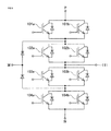
- FIG. 1 is a circuit diagram of a three-level inverter circuit that is a semiconductor device according to a first embodiment of the present invention
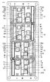
- FIG. 2 is a planar view showing chip arrangement of the three-level inverter circuit that is a semiconductor device according to the first embodiment of the present invention.
- the three-level inverter circuit is composed of first and second switching circuits connected in parallel, each switching circuit composing a three-level inverter.
- the first switching circuit comprises four IGBT chips T1, T2, T3 and T4 connected in series between a positive potential terminal P and a negative potential terminal N of a power supply, and the IGBT chips T1, T2, T3 and T4 have respective free-wheeling diodes D1, D2, D3 and D4 connected antiparallel to the respective IGBT chips T1, T2, T3 and T4.
- a clamping diode D9 is connected between the node between the IGBT chips T1 and T2 and a middle potential terminal M of the power supply.
- a clamping diode D10 is connected between the node between the IGBT chips T3 and T4 and a middle potential terminal M of the power supply.
- the second switching circuit comprises four IGBT chips T5, T6, T7 and T8 connected in series between a positive potential terminal P and a negative potential terminal N of a power supply, and the IGBT chips T5, T6, T7 and T8 have respective free-wheeling diodes D5, D6, D7 and D8 connected antiparallel to the respective IGBT chips T5, T6, T7 and T8.
- a clamping diode D11 is connected between the node between the IGBT chips T5 and T6 and a middle potential terminal M of the power supply.
- a clamping diode D12 is connected between the node between the IGBT chips T7 and T8 and a middle potential terminal M of the power supply.
- the couple of IGBT chips T1 and T5, the couple of IGBT chips T2 and T6, the couple of IGBT chips T3 and T7, and the couple of IGBT chips T4 and T8 operate to deliver the same level of potential and have a common terminal for applying a control signal.
- Each of the gate terminals of the IGBT chips T1 and T5 in the high potential side in the upper arm is connected to a common gate terminal T1G.
- a common auxiliary emitter terminal T1E which gives a base potential for the gate terminal T1G, is connected to the emitter terminal of the IGBT chip T1 and further connected to the emitter terminal of the IGBT chip T5 through an auxiliary emitter line 1.
- Each of the gate terminals of the IGBT chips T2 and T6 in the low potential side in the upper arm is connected to a common gate terminal T2G.
- a common auxiliary emitter terminal T2E is connected to the emitter terminal of the IGBT chip T2 and further connected to the emitter terminal of the IGBT chip T6 through an auxiliary emitter line 2.
- Each of the gate terminals of the IGBT chips T3 and T7 in the high potential side in the lower arm is connected to a common gate terminal T3G.
- a common auxiliary emitter terminal T3E is connected to the emitter terminal of the IGBT chip T3 and further connected to the emitter terminal of the IGBT chip T7 through an auxiliary emitter line 3.
- Each of the gate terminals of the IGBT chips T4 and T8 in the low potential side in the lower arm is connected to a common gate terminal T4G.
- a common auxiliary emitter terminal T4E is connected to the emitter terminal of the IGBT chip T4 and further connected to the emitter terminal of the IGBT chip T8 through an auxiliary emitter line.4.
- the emitter terminal of the IGBT chip T1 in the high potential side of the upper arm is connected to the emitter terminal of the IGBT chip T5 in the high potential side of the upper arm with a wiring line 5 that has a current carrying capacity approximately equal to the rated current of the IGBT chips T1 and T5 and has a resistance value lower than the auxiliary emitter line 1.
- the emitter terminal of the IGBT chip T3 in the high potential side of the lower arm is connected to the emitter terminal of the IGBT chip T7 in the high potential side of the lower arm with a wiring line 6 that has a current carrying capacity approximately equal to the rated current of the IGBT chips T3 and T7 and has a resistance value lower than the auxiliary emitter line 3.
- the node between the IGBT chips T2 and T3 is connected to the node between the IGBT chips T6 and T7 through an output line 7, and the latter node is connected through an output line 8 to an output terminal U for a U-phase, for example.
- the IGBT chips T1 through T8, the free-wheeling diodes D1 through D8, and clamping diodes D9 through D12 are accommodated in one package and compose a three-level inverter circuit module.
- the upper arm of the first switching circuit is mounted on an insulated circuit board 11.
- the insulated circuit board 11 has the IGBT chips T1 and T2, the free-wheeling diodes D1 and D2, and the clamping diode D9 mounted thereon.
- the gate terminals T1G and T2G of the IGBT chip T1 and T2 are connected to the gate line 15 and 16 respectively, and the auxiliary emitter terminals T1E and T2E are connected to the auxiliary emitter lines 1 and 2 respectively.
- the upper arm of the second switching circuit is mounted on an insulated circuit board 12.
- the insulated circuit board 12 has the IGBT chips T5 and T6, the free-wheeling diodes D5 and D6, and the clamping diode D11 mounted thereon.
- the gate terminals are connected to the gate line 15 and 16, and the auxiliary emitter terminals are connected to the auxiliary emitter lines 1 and 2.
- the parts of the gate line 15 on the insulated circuit boards 11 and 12 are connected together with a bonding wire that composes a part of the gate line 15.
- the parts of the gate line 16 on the insulated circuit boards 11 and 12 are connected together with a bonding wire that composes a part of the gate line 16.
- the parts of the auxiliary emitter line 1 on the insulated circuit boards 11 and 12 are connected together with a bonding wire that composes a part of the auxiliary emitter line 1; and the parts of the auxiliary emitter line 2 on the insulated circuit boards 11 and 12 are connected together with a bonding wire that composes a part of the auxiliary emitter line 2.
- the circuit pattern to which the emitter terminal of the IGBT chip T1 is connected with a bonding wire is connected to the circuit pattern to which the emitter terminal of the IGBT chip T5 is connected with a bonding wire, through a bonding wire corresponding to the wiring line 5 indicated in FIG. 1 .
- This bonding wire has a current carrying capacity approximately equal to the rated current of the IGBT chips T1 and T5 and has a resistance value lower than the auxiliary emitter line 1.
- this bonding wire as depicted in FIG. 2 is composed of only one wire, the bonding wire is actually composed of necessary number of parallel wires.
- the imbalance does not cause current flow through the auxiliary emitter line 1, and the current flows through the bonding wire corresponding to the wiring line 5.
- no potential difference develops in the auxiliary emitter line 1 and the IGBT chips T1 and T5 are driven under an approximately equal condition. Therefore, the power loss in the IGBT chip T5 is not larger than that in the IGBT chip T1.
- the lower arm of the first switching circuit is mounted on an insulated circuit board 13.
- the insulated circuit board 13 has the IGBT chips T3 and T4, the free-wheeling diodes D3 and D4, and the clamping diode D10 mounted thereon.
- the gate terminals T3G and T4G of the IGBT chips T3 and T4 are connected to the gate line 17 and 18 respectively, and the auxiliary emitter terminals T3E and T4E are connected to the auxiliary emitter lines 3 and 4 respectively.
- the lower arm of the second switching circuit is mounted on an insulated circuit board 14.
- the insulated circuit board 14 has the IGBT chips T7 and T8, the free-wheeling diodes D7 and D8, and the clamping diode D12 mounted thereon.
- the gate terminals of the IGBT chips T7 and T8 are connected to the gate line 17 and 18 respectively, and the auxiliary emitter terminals are connected to the auxiliary emitter lines 3 and 4 respectively.
- the parts of the gate line 17 on the insulated circuit boards 13 and 14 are connected together with a bonding wire that composes a part of the gate line 17.
- the parts of the gate line 18 on the insulated circuit boards 13 and 14 are connected together with a bonding wire that composes a part of the gate line 18.
- the parts of the auxiliary emitter line 3 on the insulated circuit boards 13 and 14 are connected together with a bonding wire that composes a part of the auxiliary emitter line 3; and the parts of the auxiliary emitter line 4 on the insulated circuit boards 13 and 14 are connected together with a bonding wire that composes a part of the auxiliary emitter line 4.
- the circuit pattern to which the emitter terminal of the IGBT chip T3 is connected with a bonding wire is connected to the circuit pattern to which the emitter terminal of the IGBT chip T7 is connected with a bonding wire, with a bonding wire corresponding to the wiring line 6 indicated in FIG. 1 .
- This bonding wire has a current carrying capacity approximately equal to the rated current of the IGBT chips T3 and T7 and has a resistance value lower than that of the auxiliary emitter line 3.
- this bonding wire as depicted in FIG. 2 is composed of only one wire, the bonding wire is actually composed of necessary number of parallel wires.
- the output lines 7 and 8 connecting to the output terminal U which are indicated in FIG. 1 , are composed of bus bars disposed outside this module, and thus not depicted in FIG. 2 .
- the wiring line 5 and the wiring line 6 are provided in order to reduce the potential difference across the auxiliary emitter line 1 for the IGBT chips T1 and T5 and the potential difference across the auxiliary emitter line 3 for the IGBT chip T3 and T7 down to such a degree that does not affect gate driving operation.
- the wiring lines 5 and 6 reduce the resistance value between the emitter terminals of the IGBT chips.
- Each of the resistance values of the wiring lines 5 and 6 is preferably at most 0.1 ohm. The reason for this resistance value is as follows.
- the rated current of IGBTs that can be manufactured in a single chip at present is in the range of about 100 to 150 amps in consideration of manufacturing process and costs; inverter circuits for larger current capacity are constructed by a plurality of chips connected in parallel.
- the gate voltage which is about 15 volts, for driving an IGBT is different by as large as 1 volt between the parallel-connected IGBTs
- parallel operation of the IGBTs cannot be performed.
- the potential difference between the emitter terminals has to be not higher than 1 volt, which leads to the resistance value of the wiring line 5 and the wiring line 6 to be not larger than 0.1 ohm.
- the resistance values of the wiring lines 5 and 6 are actually made to be in the order of 0.001 ohm, which is sufficiently smaller than the resistance value of the auxiliary emitter lines 1 and 3.
- the potential difference between the emitter terminals of the IGBTs is such a small value that does not affect gate driving operation. Therefore, the parallel-connected IGBTs allows stable gate driving operation and reduced switching loss.
- FIG. 3 is a circuit diagram of a three-level inverter circuit that is a semiconductor device according to a second embodiment of the present invention
- FIG. 4 is a planar view showing chip arrangement of the three-level inverter circuit that is a semiconductor device according to the second embodiment of the present invention.
- the components in FIG. 3 and FIG. 4 similar to those in FIG. 1 and FIG. 2 are given the same symbols.
- the three-level inverter circuit of the semiconductor device according to the second embodiment is different from the three-level inverter circuit of the semiconductor device according to the first embodiment in that the wiring line 5 provided between the emitter terminals of the IGBT chips T1 and T5 and the wiring line 6 provided between the emitter terminals of the IGBT chips T3 and T7 are changed in configuration and position as shown in FIG. 3 and FIG. 4 .
- the auxiliary emitter lines 1 and 3 in the circuit of FIG. 1 are replaced by wiring lines 5 and 6 having a larger current carrying capacity and a lower resistance value than those of the auxiliary emitter lines 1 and 3.
- the wiring line 5 is constructed by a circuit pattern, to which the auxiliary emitter terminal T1E is connected, with a shape of strips on the insulated circuit boards 11 and 12 and a bonding wire connecting the strips.
- the wiring line 6 is constructed by a circuit pattern, to which the auxiliary emitter terminal T3E is connected, with a shape of strips on the insulated circuit boards 13 and 14 and a bonding wire connecting the strips.
- FIG. 5 is a circuit diagram of a three-level inverter circuit that is a semiconductor device according to a third embodiment of the present invention.
- the components in FIG. 5 similar to those in FIG. 1 are given the same symbols.
- This three-level inverter circuit that is a semiconductor device according to a third embodiment of the present invention is different from the three-level inverter circuit that is a semiconductor device according to the first embodiment in that the three-level inverter circuit of the third embodiment comprises three parallel-connected switching circuits while the three-level inverter circuit of the first embodiment comprises two parallel-connected switching circuits.
- This three-level inverter circuit is composed of first, second and third switching circuits, each being a three-level inverter.
- the first switching circuit comprises four IGBT chips T1, T2, T3 and T4 connected in series; four free-wheeling diodes D1, D2, D3 and D4; and two clamping diodes D9 and D10.
- the second switching circuit comprises four IGBT chips T5, T6, T7 and T8 connected in series; four free-wheeling diodes D5, D6, D7 and D8; and two clamping diodes D11 and D12.
- the third switching circuit comprises four IGBT chips T13, T14, T15 and T16 connected in series; four free-wheeling diodes D13, D14, D15 and D16; and two clamping diodes D17 and D18.
- the emitter terminals of the IGBT chips T1, T5, and T13 are connected with an auxiliary emitter line 1.
- a wiring line 5 is connected in parallel to the auxiliary emitter line 1, to increase current capacity and reduce resistance value from those of the auxiliary emitter line 1.
- the emitter terminals of the IGBT chips T3, T7, and T15 are connected with an auxiliary emitter line 3.
- a wiring line 6 is connected in parallel to the auxiliary emitter line 3, to increase current capacity and reduce resistance value from those of the auxiliary emitter line 3.
- the semiconductor device according to the third embodiment is composed of three switching circuits connected in parallel, four or more switching circuits can be provided for composing a semiconductor device.
- wiring lines 5 and 6 are connected in parallel to auxiliary emitter lines 1 and 3.
- the auxiliary emitter lines 1 and 3 can be replaced by the wiring lines 5 and 6, similarly to the semiconductor device of the second embodiment.
- FIG. 6 is a circuit diagram of a five-level inverter circuit that is a semiconductor device according to a fourth embodiment of the present invention.
- the components in FIG. 6 similar to those in FIG. 1 are given the same symbols.
- This five-level inverter circuit that is a semiconductor device according to a fourth embodiment is composed of first and second switching circuits connected in parallel, each switching circuit being a five-level inverter.
- the first switching circuit comprises: eight IGBT chips T21 through T28 connected in series; eight free-wheeling diodes D21 through 28; and six clamping diodes D37 through D42.
- the second switching circuit comprises: eight IGBT chips T29 through T36 connected in series; eight free-wheeling diodes D29 through D36; and six clamping diodes D43 through D48.
- the node between the clamping diodes D37 and D38 and the node between the clamping diodes D43 and D44 are connected to a middle potential terminal Ma.
- the node between the clamping diodes D39 and D40 and the node between the clamping diodes D45 and D46 are connected to a middle potential terminal Mb.
- the node between the clamping diodes D41 and D42 and the node between the clamping diodes D47 and D48 are connected to a middle potential terminal Mc.
- the output terminal U is connected to the node between the IGBT chips T24 and T25, and to the node between the IGBT chips T32 and T33.
- wiring lines 5a, 5b and 5c connects the emitter terminals of the IGBT chips T21 and T29, the emitter terminals of the IGBT chips T22 and T30, and the emitter terminals of the IGBT chips T23 and T31, respectively.
- Wiring lines 6a, 6b, and 6c connects the emitter terminals of the IGBT chips T25 and T33, the emitter terminals of the IGBT chips T26 and T34, and the emitter terminals of the IGBT chips T27 and T35, respectively.
- This five-level inverter circuit comprises the wiring lines 5a, 5b, 5c, 6a, 6b and 6c that connect each of the pairs of series-connection nodes to which the clamping diodes D37 through D48 are connected.
- current carrying capacity is increased and the resistance value is reduced from those of the auxiliary emitter lines.
- the semiconductor device of the fourth embodiment has a construction of five-level inverter circuit
- a semiconductor device can have a construction of seven-level or higher level inverter.
- wiring lines corresponding to the wiring lines 5a, 5b, 5c, 6a, 6b and 6c are provided.
- the auxiliary emitter lines in the semiconductor device of the fourth embodiment can be eliminated leaving the wiring lines 5a, 5b, 5c, 6a, 6b and 6c, similarly to the second embodiment.
- the switching elements which are IGBTs in the embodiments described thus far, can be changed to MOSFETs (metal-oxide-semiconductor field effect transistors), SiC (silicon carbide) MOSFETs, or SiC IGBTs.
- MOSFETs metal-oxide-semiconductor field effect transistors
- SiC silicon carbide MOSFETs
- SiC IGBTs SiC IGBTs
Landscapes
- Engineering & Computer Science (AREA)
- Power Engineering (AREA)
- Inverter Devices (AREA)
- Power Conversion In General (AREA)
Abstract
Description
- This application is based on, and claims priority to, Japanese Patent Application No.
2014-183091, filed on September 9, 2014 - The present invention relates to a semiconductor device, in particular to a semiconductor device that is a power conversion module accommodating a plurality of switching elements connected in series in a package and connecting plural sets of the plurality of series-connected switching elements in parallel to increase current carrying capacity of the semiconductor device.
- Semiconductor devices for power conversion often use insulated gate bipolar transistors (IGBTs), which are power switching elements exhibiting excellent operation performances in high voltage, heavy current and high speed switching. A semiconductor device having a multilevel inverter circuit is known to meet the requirements for down-sizing and high performance. The multilevel inverter circuit outputs multi-levels of voltages in combination of plurality of IGBTs, and is disclosed in
Patent Document 1, for example. -
FIG. 7 is a circuit diagram of a one phase, three-level inverter circuit of a general construction using switching elements of IGBTs.FIG. 8 is a circuit diagram of a first example of a three-level inverter circuit with increased current carrying capacity, andFIG. 9 is a circuit diagram of a second example of a three-level inverter circuit with increased current carrying capacity. - The three-level inverter circuit of
FIG. 7 comprises: fourIGBTs wheeling diodes clamping diodes 109 and 110.TheIGBTs wheeling diodes - The IGBTs 101, 102, 103, and 104 are connected in series and the middle node is connected to an
output terminal 111. A node between theIGBT 101 and theIGBT 102 composing an upper arm of the inverter circuit is connected to aclamping diode 109. A node between theIGBT 103 and theIGBT 104 composing a lower arm of the inverter circuit is connected to aclamping diode 110. Theclamping diodes - The emitter terminal of the IGBT 104 is connected to the negative terminal potential N of a power supply. The collector terminal of the IGBT 101 is connected to the positive terminal potential P of the power supply. The node between the
clamping diodes - A voltage having three-levels of potential in each of the positive and negative sides is delivered from the
output terminal 111 by ON/OFF-controlling theIGBTs IGBTs - When each of single IGBT 101, 102, 103, and 104 cannot supply enough current carrying capacity, a plurality of IGBTs are connected in parallel. In the example of
FIG. 8 , the upper arm of the inverter circuit is composed of a series-connect two sets of modules, one set being composed of a module of anIGBT 101a and a module of anIGBT 101b connected in parallel, and another set being composed of a module of anIGBT 102a and a module of anIGBT 102b connected in parallel. The lower arm of the inverter circuit is composed of a series-connected two sets of modules, one set being composed of a module of anIGBT 103a and a module of anIGBT 103b connected in parallel, and another set being composed of a module of anIGBT 104a and a module of anIGBT 104b connected in parallel. - In the construction of the inverter circuit, the modules are prepared separately and then assembled together, leading to complicated wiring. In addition, drive circuits have to be prepared individually.
-
FIG. 9 shows another example of inverter circuit. This inverter circuit is not composed of a combination of a plurality of modules but formed of a single module that is composed of a plurality of chips combined together. The inverter circuit ofFIG. 9 is composed of two sets of circuits, each set being composed of series-connected chips and being similar to the inverter circuit ofFIG. 7 , - The upper arm of the inverter circuit comprises series-connected
IGBT chips IGBT chips IGBT chips IGBT chips IGBT chips IGBT chips corresponding IGBT chips auxiliary emitter terminal 151; and thecorresponding IGBT chips common gate terminal 142 and a commonauxiliary emitter terminal 152. Likewise, in the parallel connected circuits in the lower arm, thecorresponding IGBT chips common gate terminal 143 and a commonauxiliary emitter terminal 153; and thecorresponding IGBT chips common gate terminal 144 and a commonauxiliary emitter terminal 154. - The
auxiliary emitter terminal 151 is connected to the emitter of theIGBT chip 121 and further to the emitter of theIGBT chip 131 through anauxiliary emitter line 161. Theauxiliary emitter terminal 152 is connected to the emitter of theIGBT chip 122 and further to the emitter of theIGBT chip 132 through anauxiliary emitter line 162. Likewise, theauxiliary emitter terminal 153 is connected to the emitter of theIGBT chip 123 and further to the emitter of theIGBT chip 133 through anauxiliary emitter line 163. Theauxiliary emitter terminal 154 is connected to the emitter of theIGBT chip 124 and further to the emitter of theIGBT chip 134 through anauxiliary emitter line 164. - The node between the
IGBT chips IGBT chips output line 171, and the node between theIGBT chips output terminal 111 through anoutput line 172. - The
clamping diode 125 is connected to the node between theIGBT chips clamping diode 126 is connected to the node between theIGBT chips clamping diode 135 is connected to the node between theIGBT chips clamping diode 136 is connected to the node between theIGBT chips - A voltage with three-levels of potential in each of positive and negative sides is delivered from the
output terminal 111 by ON/OFF-controlling theIGBT chips IGBT chips IGBT chips IGBT chips - Japanese Unexamined Patent Application Publication No.
2000-060140 - In the construction of parallel-connection of series-connected circuits, imbalance of operation of corresponding IGBT chips generates a potential difference between both ends of the auxiliary emitter line, which may destroy the auxiliary emitter line by abnormal current. For example, the four
IGBT chips FIG. 9 have not necessarily equivalent characteristics, but for example ON resistances are different in the ON operation. Suppose that theIGBT chips IGBT chips IGBT chip 121 with lower ON resistance tends to carry larger current than theIGBT chip 131 with higher ON resistance; and theIGBT chip 132 with lower ON resistance tends to carry larger current than theIGBT chip 122 with higher ON resistance. As a result, the current supplied from the positive potential terminal P flows in larger amount through the path ofIGBT chip 121, theauxiliary emitter line 161, and theIGBT chip 132 to theoutput terminal 111. The current flowing in theauxiliary emitter line 161 generates potential difference between both ends of the auxiliary emitter line. As a consequence, although the same gate voltage is applied between the gate terminal 141 and theauxiliary emitter terminal 151, the voltage between the gate and emitter of theIGBT chip 121 differs from the voltage between the gate and emitter of theIGBT chip 131. Thus, theIGBT chips auxiliary emitter line 161 with a small current carrying capacity may burn out with a heavy current. - The present invention has been made in view of the problem in conventional technologies, and an object of the present invention is to provide a semiconductor device that avoids development of potential difference in the auxiliary emitter line that is a wiring line in the base potential side of the IGBT chips connected in parallel, even though imbalance in characteristics among the IGBT chips exists.
- To solve the above problem, a semiconductor device of the present invention comprises: at least two switching circuits connected in parallel, the switching circuit comprising at least two switching elements connected in series and a clamping diode connected to a node between adjacent switching elements; a base potential line connecting auxiliary terminals at a base potential for applying an equivalent control signal on the switching elements that operate to deliver an equal level of potential in the parallel-connected switching circuits. The semiconductor device comprises a wiring line that connects the corresponding nodes of the parallel-connected switching circuits and that has a current carrying capacity approximately equal to a rated current of the semiconductor element and a lower resistance value than the base potential line.
- A semiconductor device of the present invention as stated above comprises a wiring line with a large current carrying capacity and a low resistance provided in parallel to the base potential line. As a consequence, even when imbalance in characteristics exists among the switching elements constructing the switching circuits connected in parallel, heavy current does not flow through the base potential line. Therefore, potential difference does not develop in the base potential line.
- The semiconductor device having the construction described above prevents current imbalance in switching operation by providing a wiring line with a high current carrying capacity and low a resistance in parallel to the base potential line between the parallel-connected switching circuits. Therefore, switching loss in the semiconductor device is minimized.
-
-
FIG. 1 is a circuit diagram of a three-level inverter circuit that is a semiconductor device according to a first embodiment of the present invention; -
FIG. 2 is a planar view showing chip arrangement of the three-level inverter circuit that is a semiconductor device according to the first embodiment of the present invention; -
FIG. 3 is a circuit diagram of a three-level inverter circuit that is a semiconductor device according to a second embodiment of the present invention; -
FIG. 4 is a planar view showing chip arrangement of the three-level inverter circuit that is a semiconductor device according to the second embodiment of the present invention; -
FIG. 5 is a circuit diagram of a three-level inverter circuit that is a semiconductor device according to a third embodiment of the present invention; -
FIG. 6 is a circuit diagram of a five-level inverter circuit that is a semiconductor device according to a fourth embodiment of the present invention; -
FIG. 7 is a circuit diagram of a one phase, three-level inverter circuit of a general construction using switching elements of IGBTs; -
FIG. 8 is a circuit diagram of a first example of a three-level inverter circuit with increased current capacity; and -
FIG. 9 is a circuit diagram of a second example of a three-level inverter circuit with increased current capacity. - The following describes in detail, some preferred embodiments in applications to modules of multi-level inverter circuit using switching elements of IGBTs, with reference to accompanying drawings. These embodiments can be actually applied in combination of the embodiments as long as no contradiction arises.
-
FIG. 1 is a circuit diagram of a three-level inverter circuit that is a semiconductor device according to a first embodiment of the present invention; andFIG. 2 is a planar view showing chip arrangement of the three-level inverter circuit that is a semiconductor device according to the first embodiment of the present invention. - The three-level inverter circuit, as shown in
FIG. 1 , is composed of first and second switching circuits connected in parallel, each switching circuit composing a three-level inverter. The first switching circuit comprises four IGBT chips T1, T2, T3 and T4 connected in series between a positive potential terminal P and a negative potential terminal N of a power supply, and the IGBT chips T1, T2, T3 and T4 have respective free-wheeling diodes D1, D2, D3 and D4 connected antiparallel to the respective IGBT chips T1, T2, T3 and T4. A clamping diode D9 is connected between the node between the IGBT chips T1 and T2 and a middle potential terminal M of the power supply. A clamping diode D10 is connected between the node between the IGBT chips T3 and T4 and a middle potential terminal M of the power supply. Likewise, the second switching circuit comprises four IGBT chips T5, T6, T7 and T8 connected in series between a positive potential terminal P and a negative potential terminal N of a power supply, and the IGBT chips T5, T6, T7 and T8 have respective free-wheeling diodes D5, D6, D7 and D8 connected antiparallel to the respective IGBT chips T5, T6, T7 and T8. A clamping diode D11 is connected between the node between the IGBT chips T5 and T6 and a middle potential terminal M of the power supply. A clamping diode D12 is connected between the node between the IGBT chips T7 and T8 and a middle potential terminal M of the power supply. - In the first and second switching circuits, the couple of IGBT chips T1 and T5, the couple of IGBT chips T2 and T6, the couple of IGBT chips T3 and T7, and the couple of IGBT chips T4 and T8 operate to deliver the same level of potential and have a common terminal for applying a control signal. Each of the gate terminals of the IGBT chips T1 and T5 in the high potential side in the upper arm is connected to a common gate terminal T1G. A common auxiliary emitter terminal T1E, which gives a base potential for the gate terminal T1G, is connected to the emitter terminal of the IGBT chip T1 and further connected to the emitter terminal of the IGBT chip T5 through an
auxiliary emitter line 1. - Each of the gate terminals of the IGBT chips T2 and T6 in the low potential side in the upper arm is connected to a common gate terminal T2G. A common auxiliary emitter terminal T2E is connected to the emitter terminal of the IGBT chip T2 and further connected to the emitter terminal of the IGBT chip T6 through an
auxiliary emitter line 2. - Each of the gate terminals of the IGBT chips T3 and T7 in the high potential side in the lower arm is connected to a common gate terminal T3G. A common auxiliary emitter terminal T3E is connected to the emitter terminal of the IGBT chip T3 and further connected to the emitter terminal of the IGBT chip T7 through an
auxiliary emitter line 3. - Each of the gate terminals of the IGBT chips T4 and T8 in the low potential side in the lower arm is connected to a common gate terminal T4G. A common auxiliary emitter terminal T4E is connected to the emitter terminal of the IGBT chip T4 and further connected to the emitter terminal of the IGBT chip T8 through an auxiliary emitter line.4.
- The emitter terminal of the IGBT chip T1 in the high potential side of the upper arm is connected to the emitter terminal of the IGBT chip T5 in the high potential side of the upper arm with a
wiring line 5 that has a current carrying capacity approximately equal to the rated current of the IGBT chips T1 and T5 and has a resistance value lower than theauxiliary emitter line 1. Likewise, the emitter terminal of the IGBT chip T3 in the high potential side of the lower arm is connected to the emitter terminal of the IGBT chip T7 in the high potential side of the lower arm with awiring line 6 that has a current carrying capacity approximately equal to the rated current of the IGBT chips T3 and T7 and has a resistance value lower than theauxiliary emitter line 3. The node between the IGBT chips T2 and T3 is connected to the node between the IGBT chips T6 and T7 through anoutput line 7, and the latter node is connected through anoutput line 8 to an output terminal U for a U-phase, for example. - The IGBT chips T1 through T8, the free-wheeling diodes D1 through D8, and clamping diodes D9 through D12 are accommodated in one package and compose a three-level inverter circuit module.
- In this module, the upper arm of the first switching circuit is mounted on an
insulated circuit board 11. The insulatedcircuit board 11 has the IGBT chips T1 and T2, the free-wheeling diodes D1 and D2, and the clamping diode D9 mounted thereon. The gate terminals T1G and T2G of the IGBT chip T1 and T2 are connected to thegate line auxiliary emitter lines - The upper arm of the second switching circuit is mounted on an
insulated circuit board 12. The insulatedcircuit board 12 has the IGBT chips T5 and T6, the free-wheeling diodes D5 and D6, and the clamping diode D11 mounted thereon. The gate terminals are connected to thegate line auxiliary emitter lines gate line 15 on the insulatedcircuit boards gate line 15. The parts of thegate line 16 on the insulatedcircuit boards gate line 16. The parts of theauxiliary emitter line 1 on the insulatedcircuit boards auxiliary emitter line 1; and the parts of theauxiliary emitter line 2 on the insulatedcircuit boards auxiliary emitter line 2. - The circuit pattern to which the emitter terminal of the IGBT chip T1 is connected with a bonding wire is connected to the circuit pattern to which the emitter terminal of the IGBT chip T5 is connected with a bonding wire, through a bonding wire corresponding to the
wiring line 5 indicated inFIG. 1 . This bonding wire has a current carrying capacity approximately equal to the rated current of the IGBT chips T1 and T5 and has a resistance value lower than theauxiliary emitter line 1. Thus, although this bonding wire as depicted inFIG. 2 is composed of only one wire, the bonding wire is actually composed of necessary number of parallel wires. Thus, even though imbalance occurs in switching operations among the IGBT chips T1, T2, T5 and T6 in the upper arm, the imbalance does not cause current flow through theauxiliary emitter line 1, and the current flows through the bonding wire corresponding to thewiring line 5. Thus, no potential difference develops in theauxiliary emitter line 1 and the IGBT chips T1 and T5 are driven under an approximately equal condition. Therefore, the power loss in the IGBT chip T5 is not larger than that in the IGBT chip T1. - The lower arm of the first switching circuit is mounted on an
insulated circuit board 13. The insulatedcircuit board 13 has the IGBT chips T3 and T4, the free-wheeling diodes D3 and D4, and the clamping diode D10 mounted thereon. The gate terminals T3G and T4G of the IGBT chips T3 and T4 are connected to thegate line auxiliary emitter lines - The lower arm of the second switching circuit is mounted on an
insulated circuit board 14. The insulatedcircuit board 14 has the IGBT chips T7 and T8, the free-wheeling diodes D7 and D8, and the clamping diode D12 mounted thereon. The gate terminals of the IGBT chips T7 and T8 are connected to thegate line auxiliary emitter lines gate line 17 on the insulatedcircuit boards gate line 17. The parts of thegate line 18 on the insulatedcircuit boards gate line 18. The parts of theauxiliary emitter line 3 on the insulatedcircuit boards auxiliary emitter line 3; and the parts of theauxiliary emitter line 4 on the insulatedcircuit boards auxiliary emitter line 4. - The circuit pattern to which the emitter terminal of the IGBT chip T3 is connected with a bonding wire is connected to the circuit pattern to which the emitter terminal of the IGBT chip T7 is connected with a bonding wire, with a bonding wire corresponding to the
wiring line 6 indicated inFIG. 1 . This bonding wire has a current carrying capacity approximately equal to the rated current of the IGBT chips T3 and T7 and has a resistance value lower than that of theauxiliary emitter line 3. Thus, although this bonding wire as depicted inFIG. 2 is composed of only one wire, the bonding wire is actually composed of necessary number of parallel wires. Thus, even though imbalance occurs in switching operations among the IGBT chips T3, T4, T7 and T8 in the lower arm, the imbalance does not cause current flow through theauxiliary emitter line 3, and the current flows through the bonding wire corresponding to thewiring line 6. Thus, no potential difference develops in theauxiliary emitter line 3 and the IGBT chips T3 and T7 are driven under an approximately equal condition. Therefore, the power loss is reduce in total. - The
output lines FIG. 1 , are composed of bus bars disposed outside this module, and thus not depicted inFIG. 2 . - The
wiring line 5 and thewiring line 6 are provided in order to reduce the potential difference across theauxiliary emitter line 1 for the IGBT chips T1 and T5 and the potential difference across theauxiliary emitter line 3 for the IGBT chip T3 and T7 down to such a degree that does not affect gate driving operation. Thewiring lines wiring lines wiring line 5 and thewiring line 6 to be not larger than 0.1 ohm. The resistance values of thewiring lines auxiliary emitter lines -
FIG. 3 is a circuit diagram of a three-level inverter circuit that is a semiconductor device according to a second embodiment of the present invention; andFIG. 4 is a planar view showing chip arrangement of the three-level inverter circuit that is a semiconductor device according to the second embodiment of the present invention. The components inFIG. 3 andFIG. 4 similar to those inFIG. 1 andFIG. 2 are given the same symbols. - The three-level inverter circuit of the semiconductor device according to the second embodiment is different from the three-level inverter circuit of the semiconductor device according to the first embodiment in that the
wiring line 5 provided between the emitter terminals of the IGBT chips T1 and T5 and thewiring line 6 provided between the emitter terminals of the IGBT chips T3 and T7 are changed in configuration and position as shown inFIG. 3 andFIG. 4 . In the three-level inverter circuit of the semiconductor device according to the second embodiment as shown inFIG. 3 , theauxiliary emitter lines FIG. 1 are replaced bywiring lines auxiliary emitter lines - In the module shown in
FIG. 4 , thewiring line 5 is constructed by a circuit pattern, to which the auxiliary emitter terminal T1E is connected, with a shape of strips on the insulatedcircuit boards wiring line 6 is constructed by a circuit pattern, to which the auxiliary emitter terminal T3E is connected, with a shape of strips on the insulatedcircuit boards - In this three-level inverter circuit, too, even though differences in characteristics exist among the IGBT chips T1, T2, T5, and T6 in the upper arm, and among the IGBT chips T3, T4, T7, and T8 in the lower arm, the current in the switching operation due to the imbalance flows through the
wiring line 5 and thewiring line 6. This current through thewiring lines -
FIG. 5 is a circuit diagram of a three-level inverter circuit that is a semiconductor device according to a third embodiment of the present invention. The components inFIG. 5 similar to those inFIG. 1 are given the same symbols. - This three-level inverter circuit that is a semiconductor device according to a third embodiment of the present invention is different from the three-level inverter circuit that is a semiconductor device according to the first embodiment in that the three-level inverter circuit of the third embodiment comprises three parallel-connected switching circuits while the three-level inverter circuit of the first embodiment comprises two parallel-connected switching circuits.
- This three-level inverter circuit is composed of first, second and third switching circuits, each being a three-level inverter. The first switching circuit comprises four IGBT chips T1, T2, T3 and T4 connected in series; four free-wheeling diodes D1, D2, D3 and D4; and two clamping diodes D9 and D10. The second switching circuit comprises four IGBT chips T5, T6, T7 and T8 connected in series; four free-wheeling diodes D5, D6, D7 and D8; and two clamping diodes D11 and D12. The third switching circuit comprises four IGBT chips T13, T14, T15 and T16 connected in series; four free-wheeling diodes D13, D14, D15 and D16; and two clamping diodes D17 and D18.
- In the three-level inverter circuit composed of the first, second and third switching circuits, too, the emitter terminals of the IGBT chips T1, T5, and T13 are connected with an
auxiliary emitter line 1. In addition, awiring line 5 is connected in parallel to theauxiliary emitter line 1, to increase current capacity and reduce resistance value from those of theauxiliary emitter line 1. Likewise, the emitter terminals of the IGBT chips T3, T7, and T15 are connected with anauxiliary emitter line 3. In addition, awiring line 6 is connected in parallel to theauxiliary emitter line 3, to increase current capacity and reduce resistance value from those of theauxiliary emitter line 3. - Although the semiconductor device according to the third embodiment is composed of three switching circuits connected in parallel, four or more switching circuits can be provided for composing a semiconductor device. In that case, too,
wiring lines auxiliary emitter lines auxiliary emitter lines wiring lines -
FIG. 6 is a circuit diagram of a five-level inverter circuit that is a semiconductor device according to a fourth embodiment of the present invention. The components inFIG. 6 similar to those inFIG. 1 are given the same symbols. - This five-level inverter circuit that is a semiconductor device according to a fourth embodiment is composed of first and second switching circuits connected in parallel, each switching circuit being a five-level inverter. The first switching circuit comprises: eight IGBT chips T21 through T28 connected in series; eight free-wheeling diodes D21 through 28; and six clamping diodes D37 through D42. The second switching circuit comprises: eight IGBT chips T29 through T36 connected in series; eight free-wheeling diodes D29 through D36; and six clamping diodes D43 through D48.
- The node between the clamping diodes D37 and D38 and the node between the clamping diodes D43 and D44 are connected to a middle potential terminal Ma. The node between the clamping diodes D39 and D40 and the node between the clamping diodes D45 and D46 are connected to a middle potential terminal Mb. The node between the clamping diodes D41 and D42 and the node between the clamping diodes D47 and D48 are connected to a middle potential terminal Mc. The output terminal U is connected to the node between the IGBT chips T24 and T25, and to the node between the IGBT chips T32 and T33.
- In this five-level inverter circuit,
wiring lines Wiring lines - This five-level inverter circuit comprises the
wiring lines - Although the semiconductor device of the fourth embodiment has a construction of five-level inverter circuit, a semiconductor device can have a construction of seven-level or higher level inverter. In that construction, wiring lines corresponding to the
wiring lines wiring lines - The switching elements, which are IGBTs in the embodiments described thus far, can be changed to MOSFETs (metal-oxide-semiconductor field effect transistors), SiC (silicon carbide) MOSFETs, or SiC IGBTs.
-
- 1, 2, 3, 4: auxiliary emitter line
- 5, 5a, 5b, 5c, 6, 6a, 6b, 6c: wiring line
- 7, 8; output line
- 11, 12, 13, 14: insulated circuit board
- 15, 16, 17, 18: gate line
- D1, D2, D3, D4, D5, D6, D7, D8; D13, D14, D15, D16; D21, D22, D23, D24, D25, D26, D27, D28, D29, D30, D31, D32, D33, D34, D35, D36: free-wheeling diode
- D9, D10, D11, D12; D17, D18; D37, D38, D39, D40, D41, D42, D43, D44, D45, D46, D47, D48: clamping diode
- M, Ma, Mb, Mc: middle potential terminal
- N: negative potential terminal
- P: positive potential terminal
- T1, T2, T3, T4, T5, T6, T7, T8; T13, T14, T15, T16; T21, T22, T23, T24, T25, T26, T27, T28, T29, T30, T31, T32, T33, T34, T35, T36: IGBT chip
- T1E, T2E, T3E, T4E: auxiliary emitter terminal
- T1G, T2G, T3G, T4G: gate terminal
- U: output terminal
Claims (6)
- A semiconductor device comprising:at least two switching circuits connected in parallel, the switching circuit comprising at least two switching (T1,T2,T3,T4,T5,T6,T7,T8) elements connected in series and a clamping diode(D9,D10,D11,D12) connected to a node between adjacent switching elements (T1...T8);a base potential line connecting auxiliary terminals at a base potential for applying an equivalent control signal on the switching elements (T1...T8) that operates to deliver an equal level of potential in the parallel-connected switching circuits; anda wiring line(5,6) that connects the corresponding nodes of the parallel-connected switching circuits and that has a current carrying capacity approximately equal to a rated current of the semiconductor element and a lower resistance value than the base potential line.
- The semiconductor device according to claim 1, wherein the switching circuits are mounted on circuit patterns formed on individual insulated circuit boards, and the wiring line(5,6) connects the circuit patterns forming the nodes on the adjacent insulated circuit boards.
- The semiconductor device according to claim 1, wherein the switching element (T1...T8) is an IGBT chip and the wiring line (5, 6) connects emitter terminals of the IGBT chips (T1...T8) at a high potential side of series-connected IGBT chips (T1...T8).
- A semiconductor device comprising:at least two switching circuits connected in parallel, the switching circuit comprising at least two IGBT chips (T1...T8) connected in series and a clamping diode (D9...D12) connected to a node between adjacent IGBT chips (T1...T8) ;a base potential line connecting auxiliary emitter terminals (T1E...T4E) of the IGBT chips (T1...T8)that operate to deliver an equal level of potential in the parallel-connected switching circuits; anda wiring line(5,6) that connects the corresponding nodes of the parallel-connected switching circuits and that has a current carrying capacity approximately equal to a rated current of the IGBT chip (T1...T8) and a lower resistance value than the base potential line.
- A semiconductor device comprising:at least two switching circuits connected in parallel, the switching circuit comprising at least two IGBT chips (T1...T8) connected in series and a clamping diode (D9...D12) connected to a node between adjacent IGBT chips (T1...T8); andan auxiliary emitter line that connects auxiliary emitter terminals (T1E...T4E) of the IGBT chips (T1...T8)at a high potential side of the series-connected IGBT chips (T1...T8) in the parallel-connected switching circuits, and that has a current carrying capacity approximately equal to a rated current of the IGBT chip (T1...T8).
- The semiconductor device according to any one of claims 1, 4 and 5, wherein the wiring line(5,6) has a resistance value not larger than 0.1 ohm.
Applications Claiming Priority (1)
| Application Number | Priority Date | Filing Date | Title |
|---|---|---|---|
| JP2014183091A JP6413523B2 (en) | 2014-09-09 | 2014-09-09 | Semiconductor device |
Publications (2)
| Publication Number | Publication Date |
|---|---|
| EP2996233A1 true EP2996233A1 (en) | 2016-03-16 |
| EP2996233B1 EP2996233B1 (en) | 2023-03-29 |
Family
ID=53724048
Family Applications (1)
| Application Number | Title | Priority Date | Filing Date |
|---|---|---|---|
| EP15178167.1A Active EP2996233B1 (en) | 2014-09-09 | 2015-07-24 | Semiconductor device |
Country Status (4)
| Country | Link |
|---|---|
| US (1) | US9722598B2 (en) |
| EP (1) | EP2996233B1 (en) |
| JP (1) | JP6413523B2 (en) |
| CN (1) | CN105406742B (en) |
Cited By (5)
| Publication number | Priority date | Publication date | Assignee | Title |
|---|---|---|---|---|
| EP3484039A1 (en) * | 2017-11-10 | 2019-05-15 | Commissariat à l'Energie Atomique et aux Energies Alternatives | Switching module for inverter or voltage rectifier |
| WO2020239421A1 (en) * | 2019-05-26 | 2020-12-03 | Danfoss Silicon Power Gmbh | Three-level power module |
| US11532600B2 (en) | 2019-05-16 | 2022-12-20 | Danfoss Silicon Power Gmbh | Semiconductor module |
| WO2024133703A1 (en) * | 2022-12-21 | 2024-06-27 | Lightyear Ipco B.V. | Multi-level multi-step power converter |
| US12087699B2 (en) | 2019-05-16 | 2024-09-10 | Danfoss Silicon Power Gmbh | Semiconductor module |
Families Citing this family (14)
| Publication number | Priority date | Publication date | Assignee | Title |
|---|---|---|---|---|
| CN106059269B (en) * | 2016-06-22 | 2018-10-30 | 杭州飞仕得科技有限公司 | A kind of driving circuit suitable for IGBT multi-parallels |
| CN106129107B (en) * | 2016-07-01 | 2019-07-09 | 电子科技大学 | Semiconductor structure, semiconductor subassembly and power semiconductor |
| JP6794841B2 (en) * | 2017-01-13 | 2020-12-02 | 株式会社デンソー | Power converter and its manufacturing method |
| JP2020039221A (en) * | 2018-09-04 | 2020-03-12 | 株式会社日立製作所 | Electric power conversion device and electric vehicle |
| CN111801795B (en) | 2018-09-14 | 2024-11-12 | 富士电机株式会社 | Semiconductor devices |
| JP7054791B2 (en) * | 2018-09-25 | 2022-04-15 | パナソニックIpマネジメント株式会社 | Semiconductor devices and devices |
| JP7065434B2 (en) * | 2019-02-12 | 2022-05-12 | パナソニックIpマネジメント株式会社 | Power converter |
| JP7138596B2 (en) * | 2019-05-21 | 2022-09-16 | 三菱電機株式会社 | semiconductor equipment |
| CN112398322B (en) * | 2019-08-16 | 2022-09-23 | 南京南瑞继保电气有限公司 | Direct-series module, current conversion chain, current converter and control method |
| US11587853B2 (en) * | 2019-09-03 | 2023-02-21 | Mediatek Inc. | Semiconductor devices having a serial power system |
| JP7428019B2 (en) | 2020-03-06 | 2024-02-06 | 富士電機株式会社 | semiconductor module |
| EP3890179A1 (en) * | 2020-04-02 | 2021-10-06 | Siemens Aktiengesellschaft | Power converter |
| JP7359298B2 (en) * | 2020-05-07 | 2023-10-11 | 株式会社豊田自動織機 | power converter |
| CN113114061B (en) * | 2021-03-26 | 2022-06-24 | 台达电子企业管理(上海)有限公司 | Converter and method for suppressing circulating current interference of converter |
Citations (1)
| Publication number | Priority date | Publication date | Assignee | Title |
|---|---|---|---|---|
| EP0978934A2 (en) * | 1998-08-04 | 2000-02-09 | Kabushiki Kaisha Toshiba | Power conversion system |
Family Cites Families (11)
| Publication number | Priority date | Publication date | Assignee | Title |
|---|---|---|---|---|
| JPS63108649U (en) * | 1986-12-27 | 1988-07-13 | ||
| RU2190919C2 (en) * | 1998-04-28 | 2002-10-10 | Хитачи, Лтд. | Power circuit of electric power inverter |
| JP4209421B2 (en) * | 1998-04-28 | 2009-01-14 | 株式会社日立製作所 | Main circuit structure of power converter |
| JP2004187360A (en) * | 2002-11-29 | 2004-07-02 | Toshiba Corp | Gate drive circuit for voltage-driven switching element and semiconductor module |
| JP4582629B2 (en) | 2004-11-30 | 2010-11-17 | 東芝三菱電機産業システム株式会社 | 3-level inverter |
| JP4581717B2 (en) * | 2005-02-03 | 2010-11-17 | 富士電機ホールディングス株式会社 | Power semiconductor module |
| DE102008042693B4 (en) * | 2008-10-08 | 2015-10-08 | Semikron Elektronik Gmbh & Co. Kg | Method for operating a power converter circuit with voltage increase |
| EP2445110B1 (en) * | 2010-10-22 | 2014-05-14 | ABB Research Ltd | Gate driver unit for electrical switching device |
| JP5637944B2 (en) * | 2011-06-29 | 2014-12-10 | 株式会社 日立パワーデバイス | Power semiconductor module |
| CN103001573B (en) * | 2011-09-13 | 2016-03-23 | 台达电子企业管理(上海)有限公司 | Medium voltage converter drive system |
| JP2013236460A (en) * | 2012-05-09 | 2013-11-21 | Mitsubishi Electric Corp | Three-level inverter |
-
2014
- 2014-09-09 JP JP2014183091A patent/JP6413523B2/en active Active
-
2015
- 2015-07-22 US US14/806,290 patent/US9722598B2/en active Active
- 2015-07-24 EP EP15178167.1A patent/EP2996233B1/en active Active
- 2015-07-24 CN CN201510441642.XA patent/CN105406742B/en active Active
Patent Citations (2)
| Publication number | Priority date | Publication date | Assignee | Title |
|---|---|---|---|---|
| EP0978934A2 (en) * | 1998-08-04 | 2000-02-09 | Kabushiki Kaisha Toshiba | Power conversion system |
| JP2000060140A (en) * | 1998-08-04 | 2000-02-25 | Toshiba Corp | Power converter |
Cited By (8)
| Publication number | Priority date | Publication date | Assignee | Title |
|---|---|---|---|---|
| EP3484039A1 (en) * | 2017-11-10 | 2019-05-15 | Commissariat à l'Energie Atomique et aux Energies Alternatives | Switching module for inverter or voltage rectifier |
| FR3073689A1 (en) * | 2017-11-10 | 2019-05-17 | Commissariat A L'energie Atomique Et Aux Energies Alternatives | SWITCHING MODULE FOR INVERTER OR VOLTAGE RECTIFIER |
| US10601341B2 (en) | 2017-11-10 | 2020-03-24 | Commissariat à l'Energie Atomique et aux Energies Alternatives | Neutral point clamped multiple-level switching unit for voltage inverter or rectifier |
| US11532600B2 (en) | 2019-05-16 | 2022-12-20 | Danfoss Silicon Power Gmbh | Semiconductor module |
| US12087699B2 (en) | 2019-05-16 | 2024-09-10 | Danfoss Silicon Power Gmbh | Semiconductor module |
| WO2020239421A1 (en) * | 2019-05-26 | 2020-12-03 | Danfoss Silicon Power Gmbh | Three-level power module |
| US12261543B2 (en) | 2019-05-26 | 2025-03-25 | Danfoss Silicon Power Gmbh | Three-level power module |
| WO2024133703A1 (en) * | 2022-12-21 | 2024-06-27 | Lightyear Ipco B.V. | Multi-level multi-step power converter |
Also Published As
| Publication number | Publication date |
|---|---|
| US20160072499A1 (en) | 2016-03-10 |
| JP2016058515A (en) | 2016-04-21 |
| EP2996233B1 (en) | 2023-03-29 |
| JP6413523B2 (en) | 2018-10-31 |
| CN105406742B (en) | 2019-05-10 |
| CN105406742A (en) | 2016-03-16 |
| US9722598B2 (en) | 2017-08-01 |
Similar Documents
| Publication | Publication Date | Title |
|---|---|---|
| EP2996233B1 (en) | Semiconductor device | |
| CN100566106C (en) | Converter circuit for switching a large number of switching voltage levels | |
| US10439506B2 (en) | Matryoshka converter | |
| US6084788A (en) | Neutral point clamped power converter | |
| CA2620441C (en) | Converter circuit comprising distributed energy stores | |
| JP6164667B2 (en) | Power conversion circuit and device | |
| US6657874B2 (en) | Semiconductor converter circuit and circuit module | |
| CN1276927A (en) | Three-level neutral point clamping inverter circuit | |
| US7480160B2 (en) | Traction converter having a line-side four-quadrant controller, and method therefor | |
| CN101563838A (en) | Three level power converter | |
| CA2894127A1 (en) | Switching stage, energy conversion circuit, and conversion stage for wind turbines comprising the energy conversion circuit | |
| CN1826722A (en) | Rectifier circuit | |
| KR20220061989A (en) | Modular Switching Cell | |
| JP4582629B2 (en) | 3-level inverter | |
| US20230402940A1 (en) | Semiconductor module and power converter | |
| US6518821B2 (en) | Parallel circuit comprising a plurality of IGBTs | |
| EP3462594A1 (en) | Five-level converter | |
| KR101681499B1 (en) | Semiconductor Power Module with a Frame Structure for Reducing Stray Inductance | |
| JP6206090B2 (en) | 3-level power converter | |
| JP3277524B2 (en) | Semiconductor switch circuit and inverter device | |
| KR100928549B1 (en) | Switch clamp multi-level inverter | |
| Farhat et al. | On-Chip Design and Implementation of a Battery-Cell-Level Binary-Tree Multilevel Converter | |
| CN101854127B (en) | The power circuit structure of the power converter | |
| JP7803238B2 (en) | Output potential switching circuit | |
| CN102197578A (en) | Power output stage for a pulse-controlled inverter |
Legal Events
| Date | Code | Title | Description |
|---|---|---|---|
| PUAI | Public reference made under article 153(3) epc to a published international application that has entered the european phase |
Free format text: ORIGINAL CODE: 0009012 |
|
| AK | Designated contracting states |
Kind code of ref document: A1 Designated state(s): AL AT BE BG CH CY CZ DE DK EE ES FI FR GB GR HR HU IE IS IT LI LT LU LV MC MK MT NL NO PL PT RO RS SE SI SK SM TR |
|
| AX | Request for extension of the european patent |
Extension state: BA ME |
|
| 17P | Request for examination filed |
Effective date: 20160712 |
|
| RBV | Designated contracting states (corrected) |
Designated state(s): AL AT BE BG CH CY CZ DE DK EE ES FI FR GB GR HR HU IE IS IT LI LT LU LV MC MK MT NL NO PL PT RO RS SE SI SK SM TR |
|
| STAA | Information on the status of an ep patent application or granted ep patent |
Free format text: STATUS: EXAMINATION IS IN PROGRESS |
|
| 17Q | First examination report despatched |
Effective date: 20170718 |
|
| REG | Reference to a national code |
Ref country code: DE Ref legal event code: R079 Ref document number: 602015082944 Country of ref document: DE Free format text: PREVIOUS MAIN CLASS: H02M0001000000 Ipc: H02M0001088000 |
|
| RIC1 | Information provided on ipc code assigned before grant |
Ipc: H03K 17/567 20060101ALI20220905BHEP Ipc: H02M 7/497 20070101ALI20220905BHEP Ipc: H02M 7/487 20070101ALI20220905BHEP Ipc: H02M 1/088 20060101AFI20220905BHEP |
|
| GRAP | Despatch of communication of intention to grant a patent |
Free format text: ORIGINAL CODE: EPIDOSNIGR1 |
|
| STAA | Information on the status of an ep patent application or granted ep patent |
Free format text: STATUS: GRANT OF PATENT IS INTENDED |
|
| INTG | Intention to grant announced |
Effective date: 20221014 |
|
| GRAS | Grant fee paid |
Free format text: ORIGINAL CODE: EPIDOSNIGR3 |
|
| GRAA | (expected) grant |
Free format text: ORIGINAL CODE: 0009210 |
|
| STAA | Information on the status of an ep patent application or granted ep patent |
Free format text: STATUS: THE PATENT HAS BEEN GRANTED |
|
| AK | Designated contracting states |
Kind code of ref document: B1 Designated state(s): AL AT BE BG CH CY CZ DE DK EE ES FI FR GB GR HR HU IE IS IT LI LT LU LV MC MK MT NL NO PL PT RO RS SE SI SK SM TR |
|
| REG | Reference to a national code |
Ref country code: GB Ref legal event code: FG4D |
|
| REG | Reference to a national code |
Ref country code: CH Ref legal event code: EP |
|
| REG | Reference to a national code |
Ref country code: DE Ref legal event code: R096 Ref document number: 602015082944 Country of ref document: DE |
|
| REG | Reference to a national code |
Ref country code: AT Ref legal event code: REF Ref document number: 1557358 Country of ref document: AT Kind code of ref document: T Effective date: 20230415 |
|
| REG | Reference to a national code |
Ref country code: IE Ref legal event code: FG4D |
|
| REG | Reference to a national code |
Ref country code: LT Ref legal event code: MG9D |
|
| PG25 | Lapsed in a contracting state [announced via postgrant information from national office to epo] |
Ref country code: RS Free format text: LAPSE BECAUSE OF FAILURE TO SUBMIT A TRANSLATION OF THE DESCRIPTION OR TO PAY THE FEE WITHIN THE PRESCRIBED TIME-LIMIT Effective date: 20230329 Ref country code: NO Free format text: LAPSE BECAUSE OF FAILURE TO SUBMIT A TRANSLATION OF THE DESCRIPTION OR TO PAY THE FEE WITHIN THE PRESCRIBED TIME-LIMIT Effective date: 20230629 Ref country code: LV Free format text: LAPSE BECAUSE OF FAILURE TO SUBMIT A TRANSLATION OF THE DESCRIPTION OR TO PAY THE FEE WITHIN THE PRESCRIBED TIME-LIMIT Effective date: 20230329 Ref country code: LT Free format text: LAPSE BECAUSE OF FAILURE TO SUBMIT A TRANSLATION OF THE DESCRIPTION OR TO PAY THE FEE WITHIN THE PRESCRIBED TIME-LIMIT Effective date: 20230329 Ref country code: HR Free format text: LAPSE BECAUSE OF FAILURE TO SUBMIT A TRANSLATION OF THE DESCRIPTION OR TO PAY THE FEE WITHIN THE PRESCRIBED TIME-LIMIT Effective date: 20230329 |
|
| REG | Reference to a national code |
Ref country code: NL Ref legal event code: MP Effective date: 20230329 |
|
| REG | Reference to a national code |
Ref country code: AT Ref legal event code: MK05 Ref document number: 1557358 Country of ref document: AT Kind code of ref document: T Effective date: 20230329 |
|
| PG25 | Lapsed in a contracting state [announced via postgrant information from national office to epo] |
Ref country code: SE Free format text: LAPSE BECAUSE OF FAILURE TO SUBMIT A TRANSLATION OF THE DESCRIPTION OR TO PAY THE FEE WITHIN THE PRESCRIBED TIME-LIMIT Effective date: 20230329 Ref country code: NL Free format text: LAPSE BECAUSE OF FAILURE TO SUBMIT A TRANSLATION OF THE DESCRIPTION OR TO PAY THE FEE WITHIN THE PRESCRIBED TIME-LIMIT Effective date: 20230329 Ref country code: GR Free format text: LAPSE BECAUSE OF FAILURE TO SUBMIT A TRANSLATION OF THE DESCRIPTION OR TO PAY THE FEE WITHIN THE PRESCRIBED TIME-LIMIT Effective date: 20230630 Ref country code: FI Free format text: LAPSE BECAUSE OF FAILURE TO SUBMIT A TRANSLATION OF THE DESCRIPTION OR TO PAY THE FEE WITHIN THE PRESCRIBED TIME-LIMIT Effective date: 20230329 |
|
| PG25 | Lapsed in a contracting state [announced via postgrant information from national office to epo] |
Ref country code: SM Free format text: LAPSE BECAUSE OF FAILURE TO SUBMIT A TRANSLATION OF THE DESCRIPTION OR TO PAY THE FEE WITHIN THE PRESCRIBED TIME-LIMIT Effective date: 20230329 Ref country code: RO Free format text: LAPSE BECAUSE OF FAILURE TO SUBMIT A TRANSLATION OF THE DESCRIPTION OR TO PAY THE FEE WITHIN THE PRESCRIBED TIME-LIMIT Effective date: 20230329 Ref country code: PT Free format text: LAPSE BECAUSE OF FAILURE TO SUBMIT A TRANSLATION OF THE DESCRIPTION OR TO PAY THE FEE WITHIN THE PRESCRIBED TIME-LIMIT Effective date: 20230731 Ref country code: ES Free format text: LAPSE BECAUSE OF FAILURE TO SUBMIT A TRANSLATION OF THE DESCRIPTION OR TO PAY THE FEE WITHIN THE PRESCRIBED TIME-LIMIT Effective date: 20230329 Ref country code: EE Free format text: LAPSE BECAUSE OF FAILURE TO SUBMIT A TRANSLATION OF THE DESCRIPTION OR TO PAY THE FEE WITHIN THE PRESCRIBED TIME-LIMIT Effective date: 20230329 Ref country code: AT Free format text: LAPSE BECAUSE OF FAILURE TO SUBMIT A TRANSLATION OF THE DESCRIPTION OR TO PAY THE FEE WITHIN THE PRESCRIBED TIME-LIMIT Effective date: 20230329 |
|
| PG25 | Lapsed in a contracting state [announced via postgrant information from national office to epo] |
Ref country code: SK Free format text: LAPSE BECAUSE OF FAILURE TO SUBMIT A TRANSLATION OF THE DESCRIPTION OR TO PAY THE FEE WITHIN THE PRESCRIBED TIME-LIMIT Effective date: 20230329 Ref country code: PL Free format text: LAPSE BECAUSE OF FAILURE TO SUBMIT A TRANSLATION OF THE DESCRIPTION OR TO PAY THE FEE WITHIN THE PRESCRIBED TIME-LIMIT Effective date: 20230329 Ref country code: IS Free format text: LAPSE BECAUSE OF FAILURE TO SUBMIT A TRANSLATION OF THE DESCRIPTION OR TO PAY THE FEE WITHIN THE PRESCRIBED TIME-LIMIT Effective date: 20230729 |
|
| REG | Reference to a national code |
Ref country code: DE Ref legal event code: R097 Ref document number: 602015082944 Country of ref document: DE |
|
| PG25 | Lapsed in a contracting state [announced via postgrant information from national office to epo] |
Ref country code: DK Free format text: LAPSE BECAUSE OF FAILURE TO SUBMIT A TRANSLATION OF THE DESCRIPTION OR TO PAY THE FEE WITHIN THE PRESCRIBED TIME-LIMIT Effective date: 20230329 Ref country code: CZ Free format text: LAPSE BECAUSE OF FAILURE TO SUBMIT A TRANSLATION OF THE DESCRIPTION OR TO PAY THE FEE WITHIN THE PRESCRIBED TIME-LIMIT Effective date: 20230329 |
|
| PLBE | No opposition filed within time limit |
Free format text: ORIGINAL CODE: 0009261 |
|
| STAA | Information on the status of an ep patent application or granted ep patent |
Free format text: STATUS: NO OPPOSITION FILED WITHIN TIME LIMIT |
|
| PG25 | Lapsed in a contracting state [announced via postgrant information from national office to epo] |
Ref country code: MC Free format text: LAPSE BECAUSE OF FAILURE TO SUBMIT A TRANSLATION OF THE DESCRIPTION OR TO PAY THE FEE WITHIN THE PRESCRIBED TIME-LIMIT Effective date: 20230329 |
|
| PG25 | Lapsed in a contracting state [announced via postgrant information from national office to epo] |
Ref country code: MC Free format text: LAPSE BECAUSE OF FAILURE TO SUBMIT A TRANSLATION OF THE DESCRIPTION OR TO PAY THE FEE WITHIN THE PRESCRIBED TIME-LIMIT Effective date: 20230329 |
|
| REG | Reference to a national code |
Ref country code: CH Ref legal event code: PL |
|
| 26N | No opposition filed |
Effective date: 20240103 |
|
| REG | Reference to a national code |
Ref country code: BE Ref legal event code: MM Effective date: 20230731 |
|
| PG25 | Lapsed in a contracting state [announced via postgrant information from national office to epo] |
Ref country code: LU Free format text: LAPSE BECAUSE OF NON-PAYMENT OF DUE FEES Effective date: 20230724 |
|
| GBPC | Gb: european patent ceased through non-payment of renewal fee |
Effective date: 20230724 |
|
| PG25 | Lapsed in a contracting state [announced via postgrant information from national office to epo] |
Ref country code: LU Free format text: LAPSE BECAUSE OF NON-PAYMENT OF DUE FEES Effective date: 20230724 |
|
| REG | Reference to a national code |
Ref country code: IE Ref legal event code: MM4A |
|
| PG25 | Lapsed in a contracting state [announced via postgrant information from national office to epo] |
Ref country code: CH Free format text: LAPSE BECAUSE OF NON-PAYMENT OF DUE FEES Effective date: 20230731 Ref country code: GB Free format text: LAPSE BECAUSE OF NON-PAYMENT OF DUE FEES Effective date: 20230724 |
|
| PG25 | Lapsed in a contracting state [announced via postgrant information from national office to epo] |
Ref country code: SI Free format text: LAPSE BECAUSE OF FAILURE TO SUBMIT A TRANSLATION OF THE DESCRIPTION OR TO PAY THE FEE WITHIN THE PRESCRIBED TIME-LIMIT Effective date: 20230329 |
|
| PG25 | Lapsed in a contracting state [announced via postgrant information from national office to epo] |
Ref country code: SI Free format text: LAPSE BECAUSE OF FAILURE TO SUBMIT A TRANSLATION OF THE DESCRIPTION OR TO PAY THE FEE WITHIN THE PRESCRIBED TIME-LIMIT Effective date: 20230329 Ref country code: IT Free format text: LAPSE BECAUSE OF FAILURE TO SUBMIT A TRANSLATION OF THE DESCRIPTION OR TO PAY THE FEE WITHIN THE PRESCRIBED TIME-LIMIT Effective date: 20230329 Ref country code: FR Free format text: LAPSE BECAUSE OF NON-PAYMENT OF DUE FEES Effective date: 20230731 Ref country code: BE Free format text: LAPSE BECAUSE OF NON-PAYMENT OF DUE FEES Effective date: 20230731 |
|
| PG25 | Lapsed in a contracting state [announced via postgrant information from national office to epo] |
Ref country code: IE Free format text: LAPSE BECAUSE OF NON-PAYMENT OF DUE FEES Effective date: 20230724 |
|
| PG25 | Lapsed in a contracting state [announced via postgrant information from national office to epo] |
Ref country code: IE Free format text: LAPSE BECAUSE OF NON-PAYMENT OF DUE FEES Effective date: 20230724 |
|
| PG25 | Lapsed in a contracting state [announced via postgrant information from national office to epo] |
Ref country code: BG Free format text: LAPSE BECAUSE OF FAILURE TO SUBMIT A TRANSLATION OF THE DESCRIPTION OR TO PAY THE FEE WITHIN THE PRESCRIBED TIME-LIMIT Effective date: 20230329 |
|
| PG25 | Lapsed in a contracting state [announced via postgrant information from national office to epo] |
Ref country code: BG Free format text: LAPSE BECAUSE OF FAILURE TO SUBMIT A TRANSLATION OF THE DESCRIPTION OR TO PAY THE FEE WITHIN THE PRESCRIBED TIME-LIMIT Effective date: 20230329 |
|
| PG25 | Lapsed in a contracting state [announced via postgrant information from national office to epo] |
Ref country code: CY Free format text: LAPSE BECAUSE OF FAILURE TO SUBMIT A TRANSLATION OF THE DESCRIPTION OR TO PAY THE FEE WITHIN THE PRESCRIBED TIME-LIMIT; INVALID AB INITIO Effective date: 20150724 |
|
| PG25 | Lapsed in a contracting state [announced via postgrant information from national office to epo] |
Ref country code: HU Free format text: LAPSE BECAUSE OF FAILURE TO SUBMIT A TRANSLATION OF THE DESCRIPTION OR TO PAY THE FEE WITHIN THE PRESCRIBED TIME-LIMIT; INVALID AB INITIO Effective date: 20150724 |
|
| PGFP | Annual fee paid to national office [announced via postgrant information from national office to epo] |
Ref country code: DE Payment date: 20250528 Year of fee payment: 11 |
|
| PG25 | Lapsed in a contracting state [announced via postgrant information from national office to epo] |
Ref country code: TR Free format text: LAPSE BECAUSE OF FAILURE TO SUBMIT A TRANSLATION OF THE DESCRIPTION OR TO PAY THE FEE WITHIN THE PRESCRIBED TIME-LIMIT Effective date: 20230329 |