EP2995965A1 - Semiconductor inspection apparatus - Google Patents
Semiconductor inspection apparatus Download PDFInfo
- Publication number
- EP2995965A1 EP2995965A1 EP15174843.1A EP15174843A EP2995965A1 EP 2995965 A1 EP2995965 A1 EP 2995965A1 EP 15174843 A EP15174843 A EP 15174843A EP 2995965 A1 EP2995965 A1 EP 2995965A1
- Authority
- EP
- European Patent Office
- Prior art keywords
- voltage
- diode
- electrically connected
- detecting unit
- hemt
- Prior art date
- Legal status (The legal status is an assumption and is not a legal conclusion. Google has not performed a legal analysis and makes no representation as to the accuracy of the status listed.)
- Granted
Links
Images






Classifications
-
- G—PHYSICS
- G01—MEASURING; TESTING
- G01R—MEASURING ELECTRIC VARIABLES; MEASURING MAGNETIC VARIABLES
- G01R31/00—Arrangements for testing electric properties; Arrangements for locating electric faults; Arrangements for electrical testing characterised by what is being tested not provided for elsewhere
- G01R31/26—Testing of individual semiconductor devices
- G01R31/2607—Circuits therefor
- G01R31/2621—Circuits therefor for testing field effect transistors, i.e. FET's
-
- H—ELECTRICITY
- H10—SEMICONDUCTOR DEVICES; ELECTRIC SOLID-STATE DEVICES NOT OTHERWISE PROVIDED FOR
- H10D—INORGANIC ELECTRIC SEMICONDUCTOR DEVICES
- H10D30/00—Field-effect transistors [FET]
- H10D30/40—FETs having zero-dimensional [0D], one-dimensional [1D] or two-dimensional [2D] charge carrier gas channels
- H10D30/47—FETs having zero-dimensional [0D], one-dimensional [1D] or two-dimensional [2D] charge carrier gas channels having two-dimensional [2D] charge carrier gas channels, e.g. nanoribbon FETs or high electron mobility transistors [HEMT]
- H10D30/471—High electron mobility transistors [HEMT] or high hole mobility transistors [HHMT]
- H10D30/475—High electron mobility transistors [HEMT] or high hole mobility transistors [HHMT] having wider bandgap layer formed on top of lower bandgap active layer, e.g. undoped barrier HEMTs such as i-AlGaN/GaN HEMTs
- H10D30/4755—High electron mobility transistors [HEMT] or high hole mobility transistors [HHMT] having wider bandgap layer formed on top of lower bandgap active layer, e.g. undoped barrier HEMTs such as i-AlGaN/GaN HEMTs having wide bandgap charge-carrier supplying layers, e.g. modulation doped HEMTs such as n-AlGaAs/GaAs HEMTs
-
- H—ELECTRICITY
- H10—SEMICONDUCTOR DEVICES; ELECTRIC SOLID-STATE DEVICES NOT OTHERWISE PROVIDED FOR
- H10D—INORGANIC ELECTRIC SEMICONDUCTOR DEVICES
- H10D62/00—Semiconductor bodies, or regions thereof, of devices having potential barriers
- H10D62/80—Semiconductor bodies, or regions thereof, of devices having potential barriers characterised by the materials
- H10D62/85—Semiconductor bodies, or regions thereof, of devices having potential barriers characterised by the materials being Group III-V materials, e.g. GaAs
- H10D62/8503—Nitride Group III-V materials, e.g. AlN or GaN
Definitions
- Embodiments described herein relate generally to a semiconductor inspection apparatus.
- GaN gallium nitride
- Si silicon
- HEMT High Electron Mobility Transistor
- 2DEG two-dimensional electron gas
- the current collapse is a phenomenon that the application of high drain voltage to a field effect transistor results in increase of on-resistance. To predict the influence of the current collapse on a circuit configured to operate at a high frequency, it is preferable to evaluate the current collapse occurring just after the switching of the field effect transistor.
- the semiconductor inspection apparatus includes a first detecting unit capable of being electrically connected to a source electrode of a field effect transistor to be evaluated, the first detecting unit used for detecting voltage; a first diode including a first anode electrode and a first cathode electrode, the first cathode electrode capable of being electrically connected to a drain electrode of the field effect transistor; a second detecting unit electrically connected to the first anode electrode, the second detecting unit used for detecting voltage; a first resistance element of which a first end is electrically connected to the first anode electrode; and a first electric power source electrically connected to a second end of the first resistance element.
- GaN gallium nitride
- AlN aluminum nitride
- InN indium nitride
- GaN based semiconductor semiconductors including gallium nitride (GaN), aluminum nitride (AlN), indium nitride (InN), and their intermediate compositions are collectively referred to as a "GaN based semiconductor”.
- a semiconductor inspection apparatus of the present embodiment includes: a first detecting unit capable of being electrically connected to a source electrode of a field effect transistor to be evaluated, the first detecting unit used for detecting voltage; a first diode including a first anode electrode and a first cathode electrode, the first cathode electrode capable of being electrically connected to a drain electrode of the field effect transistor; a second detecting unit electrically connected to the first anode electrode, the second detecting unit used for detecting voltage; a first resistance element of which a first end is electrically connected to the first anode electrode; and a first electric power source electrically connected to a second end of the first resistance element.
- FIG. 1 is a circuit diagram of the semiconductor inspection apparatus according to the present embodiment.
- the semiconductor inspection apparatus of the present embodiment is configured to inspect an HEMT 10 of a GaN based semiconductor.
- the HEMT of the GaN based semiconductor is an exemplary field effect transistor.
- the HEMT 10 includes a source electrode 10a, a drain electrode 10b, and a gate electrode 10c.
- the semiconductor inspection apparatus according to the present embodiment is configured to evaluate the current collapse in the HEMT 10.
- the semiconductor inspection apparatus includes a first detecting unit 12, a second detecting unit 14, a first diode 16, a first resistance element (first electric resistance) 18, a first electric power source 20, a second resistance element (second electric resistance) 22, a second electric power source 24, a gate drive circuit 26, and a measuring instrument 28.
- the first diode 16 includes a first anode electrode 16a and a first cathode electrode 16b.
- the first cathode electrode 16b of the first diode 16 is electrically connected to the drain electrode 10b of the HEMT 10.
- a first end of the first resistance element 18 is electrically connected to the first anode electrode 16a of the first diode 16.
- a second end of the first resistance element 18 is electrically connected to the first electric power source 20.
- the first detecting unit 12 is electrically connected to the source electrode 10a of the HEMT 10. In the present embodiment, the first detecting unit 12 and the source electrode 10a are fixed at ground potentials, respectively.
- the second detecting unit 14 is electrically connected to the first anode electrode 16a of the first diode 16.
- a first end of the second resistance element 22 is electrically connected to the drain electrode 10b of the HEMT 10.
- a second end of the second resistance element 22 is electrically connected to the second electric power source 24.
- the gate drive circuit 26 is electrically connected to the gate electrode 10c of the HEMT 10.
- the measuring instrument 28 is electrically connected to the first detecting unit 12 and the second detecting unit 14.
- the HEMT 10 to be inspected is, for example, formed on a semiconductor wafer and is electrically connected to the semiconductor inspection apparatus through a probe.
- the HEMT 10 is implemented, for example, in a package and is electrically connected to the semiconductor inspection apparatus through a socket.
- the second electric power source 24 is electrically connected to the drain electrode 10b while the second resistance element 22 working as a load is held therebetween.
- the second electric power source 24 applies a test voltage V 2 to the drain electrode 10b.
- the test voltage V 2 is, for example, between 100 and 500 V.
- the second electric power source 24 is, for example, a power circuit.
- the gate drive circuit 26 controls a gate voltage to be applied to the gate electrode 10c of the HEMT 10.
- the gate drive circuit 26 controls the on and off of the HEMT 10.
- the gate drive circuit 26 includes, for example, a pulse voltage generation circuit 30 and a resistance element 32.
- the gate voltage is, for example, 0 V when the HEMT 10 is off, and between 5 and 30 V when the HEMT 10 is on.
- the drain voltage of the HEMT 10 is denoted with Vd and the drain current is denoted with Id.
- the drain voltage Vd is a high voltage equivalent to the test voltage V 2 .
- the first diode 16 has a function of blocking a high voltage from being applied to the second detecting unit 14 when the HEMT 10 is off.
- the breakdown voltage of the first diode 16 is higher than the drain voltage Vd applied to the drain electrode 10b of the HEMT 10. In other words, the breakdown voltage of the first diode 16 is higher than the test voltage V 2 .
- the first diode 16 is, for example, a pn diode made of silicon (Si).
- the first electric power source 20 has a function of charging the first anode electrode 16a of the first diode 16 when the HEMT 10 is on.
- the first electric power source 20 is, for example, a power circuit.
- the voltage of the first electric power source 20 is lower than the test voltage V 2 that the second electric power source 24 applies to the drain electrode 10b.
- the test voltage V 2 that the second electric power source 24 applies to the drain electrode 10b is higher than the voltage of the first electric power source 20.
- the setting for the voltage of the first electric power source 20 is configured to be a higher voltage than the drain voltage Vd when the HEMT 10 is on.
- the voltage of the first electric power source 20 is denoted with V 1 .
- the voltage V 1 of the first electric power source 20 is, for example, between 5 and 30 V.
- the first resistance element 18 determines the current that flows from the first electric power source 20 to the first diode 16.
- a relationship of R 1 ⁇ 10V 1 /Id is preferably satisfied when the resistance value of the first resistance element is R 1 .
- the drain voltage Vd of the HEMT 10 may indirectly be measured with the first detecting unit 12 and the second detecting unit 14.
- Each of the first detecting unit 12 and the second detecting unit 14 is, for example, an electric terminal to which a probe electrically connected to the measuring instrument 28 may be connected.
- each of the first detecting unit 12 and the second detecting unit 14 needs only to be a portion at the same potential as that of the source electrode 10a of the HEMT 10 and the first anode electrode 16a of the first diode 16.
- Each of the first detecting unit 12 and the second detecting unit 14 is not necessarily an independent unit such as an electric terminal.
- Each of the first detecting unit 12 and the second detecting unit 14 may, for example, be a part of electric wiring.
- the measuring instrument 28 has a function of measuring the voltage between the first detecting unit 12 and the second detecting unit 14.
- the measuring instrument 28 is, for example, an oscilloscope.
- the measuring instrument 28 is, for example, electrically connected to the first detecting unit 12 and the second detecting unit 14 through a probe.
- the measuring instrument 28 may directly be connected to the first detecting unit 12 and the second detecting unit 14, for example, by electric wiring.
- the HEMT 10 of the GaN based semiconductor of which current collapse is to be evaluated is prepared.
- the initial on-resistance of the HEMT 10 before the application of the test voltage is previously and separately found by measurement.
- a forward voltage drop Vf of the first diode 16 is previously and separately found.
- the source electrode 10a, the drain electrode 10b, and the gate electrode 10c of the HEMT 10 are electrically connected to the semiconductor inspection apparatus.
- the method for connection is not especially limited. A method in which the electrodes are inserted in sockets or a method in which probes have contact with the electrodes may be used according to the aspect of the HEMT 10.
- test voltage V 2 is applied to the drain electrode 10b with the second electric power source 24.
- the voltage V 1 lower than the test voltage V 2 is applied to the first anode electrode 16a of the first diode 16 with the first electric power source 20.
- a positive voltage is applied to the gate electrode 10c with the gate drive circuit 26 and the HEMT 10 is switched to on. Furthermore, the HEMT 10 may continuously be switched to repeat on and off.
- the voltage between the first detecting unit 12 and the second detecting unit 14 is measured with the measuring instrument 28.
- the voltage between the first detecting unit 12 and the second detecting unit 14 is the sum of the drain voltage Vd and the forward voltage drop Vf of the first diode 16 when the HEMT 10 is on.
- taking the difference between the measured voltage and the forward voltage drop Vf can find the drain voltage Vd.
- the drain current Id may be found, for example, from the resistance value of the second resistance element 22, and the difference between the test voltage V 2 and the drain voltage Vd, with Ohm's law. Alternatively, the drain current Id may directly be measured, for example, by insertion of a sense resistor, or with a current probe.
- the on-resistance of the HEMT 10 after the application of the test voltage V 2 may be found.
- the comparison between the on-resistance after the application of the test voltage V 2 and the initial on-resistance may find the increment of the on-resistance due to the current collapse.
- FIGS. 2A and 2B are explanatory diagrams of the semiconductor inspection apparatus according to a first comparative embodiment.
- FIG. 2A is a circuit diagram
- FIG. 2B is a diagram of the time variation in detection voltage.
- the first comparative embodiment does not include a first diode 16, a first resistance element 18, and a first electric power source 20.
- the first comparative embodiment directly measures the drain voltage Vd by measuring a voltage (detection voltage) between a first detecting unit 12 and a second detecting unit 14.
- the detection voltage is a high test voltage V 2 , for example, of hundreds of volts when the HEMT 10 is off.
- the detection voltage is a low voltage, for example, of several volts as a result from the resistive division of the on-resistance of the HEMT 10 and the second resistance element 22 working as a load when the HEMT 10 is on.
- setting the measurement range of the oscilloscope which is an example of the measuring instrument 28, at a range appropriate to the test voltage V 2 makes it difficult to measure the drain voltage Vd due to the SN ratio and/or the resolution.
- setting the measurement range of the oscilloscope at a range appropriate to the drain voltage Vd when the HEMT 10 is on makes it difficult to measure the drain voltage Vd accurately because of the saturation of the oscilloscope and/or the saturation of the probe connecting the oscilloscope to the first detecting unit 12 and the second detecting unit 14.
- FIG. 3 is a diagram of the characteristics of the drain voltage and drain current of a field effect transistor. For example, to evaluate the circuit operation of a power circuit using the field effect transistor as a switching device, the measurement of characteristics of the field effect transistor in a linear region is required.
- one method to avoid the problem caused by the SN ratio and/or the resolution in the first comparative embodiment is to set the resistance value of the second resistance element 22 to make the drain voltage Vd high when the HEMT 10 is on.
- such setting causes a problem that the current collapse of the HEMT 10 in the linear region is not evaluated.
- FIGS. 4A and 4B are explanatory diagrams of the semiconductor inspection apparatus according to a second comparative embodiment.
- FIG. 4A is a circuit diagram
- FIG. 4B is a diagram of the time variation in detection voltage.
- the second comparative embodiment is further provided with a resistance element 34 and a resistance element 36 in addition to the first comparative embodiment.
- Providing the resistance element 34 and resistance element 36 of high-resistance can reduce the detection voltage when the HEMT 10 is off, using the effect of resistive division. This makes it possible to avoid the problem caused by the SN ratio and/or the resolution.
- a CR delay due to the resistance element 34 and resistance element 36 of high resistance and/or the parasitic capacitance of the probe occurs in the second comparative embodiment.
- the waveform just after the switching of the HEMT 10 from off-state to on-state is rounded off, as illustrated in FIG. 4B .
- the waveform of the detection voltage when current collapse occurs shows a similar movement.
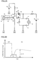
- FIGS. 5A and 5B are explanatory diagrams of the function of the semiconductor inspection apparatus according to the present first embodiment.
- FIG. 5A is a circuit diagram
- FIG. 5B is a diagram of the time variation in detection voltage.
- the test voltage V 2 is blocked by the first diode 16 when the HEMT 10 is off.
- the detection voltage when the HEMT 10 is off is the voltage V 1 applied by the first electric power source 20.
- the voltage V 1 is set at a lower value than the test voltage V 2 .
- a higher voltage of the second detecting unit 14 than the drain voltage Vd causes a forward current to flow in the first diode 16.
- the detection voltage in such a state is the sum of the drain voltage Vd and the forward voltage drop Vf of the first diode 16.
- the detection voltage when the HEMT 10 is off is the voltage V 1 lower than the test voltage V 2 .
- the difference of the detection voltages when the HEMT 10 is off-state and on-state decreases. This solves the problem caused by the SN ratio or the resolution.
- the increase in drain voltage Vd is not required. Thus, the current collapse in the linear region may be observed and evaluated.
- the movement of the observed waveform just after the switching of the HEMT 10 can be opposite to the movement when current collapse occurs. This makes it easy to observe the on-resistance just after the switching called dynamic on-resistance. Thus, the current collapse can accurately be evaluated just after the switching.
- the parasitic capacitance can be decreased in comparison to the second comparative embodiment. This suppress the CR delay. This also enables the current collapse to be evaluated accurately just after the switching.
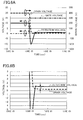
- FIGS. 6A and 6B are diagrams of the simulation results of the semiconductor inspection apparatus according to the present embodiment.
- FIG. 6A illustrates the time variation in each of the gate voltage, the drain voltage, and the detection voltage.
- FIG. 6B is an enlarged view of a region just after the switching illustrated in FIG. 6A , and illustrates the drain voltage and the detection voltage.
- the drain voltage Vd is a high voltage (400 V) whereas the detection voltage is maintained at the voltage V 1 (10 V) of the first electric power source 20.
- the gate voltage changes from zero V to a positive voltage (15 V) and the HEMT 10 is on.
- the detection voltage temporarily drops from zero V and then increases.
- the detection voltage is the sum of the drain voltage Vd and the forward voltage drop Vf of the first diode 16, as illustrated in FIG. 6B .
- the difference between the detection voltage and the drain voltage Vd is the forward voltage drop Vf.
- FIG. 7 is a diagram of the measurement results of the on-resistance by the semiconductor inspection apparatus according to the present embodiment, and illustrates the time variation in on-resistance. The time elapsed after a positive voltage is applied to the gate voltage and the HEMT 10 is switched to on is shown on the horizontal axis.
- the on-resistance can be measured from a short time of 20 nanoseconds after the HEMT 10 is switched.
- the present embodiment can provide a semiconductor inspection apparatus that can evaluate the current collapse from a short period of time after the switching.
- a relationship of R 1 ⁇ 10V 1 /Id is preferably satisfied when the drain current of the field effect transistor is Id, the voltage of the first electric power source 20 is V 1 , and the resistance value of the first resistance element 18 is R 1 . Satisfying the relationship makes the current flowing from the first diode 16 toward the drain electrode 10b when the HEMT 10 is on equal to or less than a tenth of the drain current Id. This can suppress the influence of the current flowing from the first diode 16 toward the drain electrode 10b on the measurement of the drain voltage Vd. Furthermore, in terms of the reduction in influence, a relationship of R 1 ⁇ 100V 1 /Id is more preferably satisfied.
- the first diode 16 is preferably a fast recovery diode.
- the fast recovery diode has an excellent recovery characteristic, and thus can accelerate the evaluation especially when the HEMT 10 is continuously switched.
- the first diode 16 is also preferably a Schottky barrier diode made of SiC.
- the Schottky barrier diode made of SiC has an excellent temperature characteristic, and thus improves the accuracy of measurement of a voltage.
- the Schottky barrier diode made of SiC has also an excellent recovery characteristic, and thus can accelerate the evaluation especially when the HEMT 10 is continuously switched.
- the semiconductor inspection apparatus includes the second resistance element 22, the second electric power source 24, the gate drive circuit 26, and the measuring instrument 28 is described in the present embodiment.
- the semiconductor inspection apparatus can also include the components outside the inspection apparatus.
- a semiconductor inspection apparatus configured to evaluate current collapse may include the first detecting unit 12, the second detecting unit 14, the first diode 16, the first resistance element 18, and the first electric power source 20.
- a transistor evaluation system may include components corresponding to the second resistance element 22, the second electric power source 24, and the gate drive circuit 26.
- the semiconductor inspection apparatus may be connected to the transistor evaluation system.
- the measuring instrument 28 may be externally connected to the first detecting unit 12 and the second detecting unit 14.
- the semiconductor inspection apparatus is similar to the semiconductor inspection apparatus of the first embodiment except for further including a second diode including a second anode electrode electrically connected to a first detecting unit and a second cathode electrode electrically connected to a second detecting unit.
- a second diode including a second anode electrode electrically connected to a first detecting unit and a second cathode electrode electrically connected to a second detecting unit.
- FIG. 8 is a circuit diagram of the semiconductor inspection apparatus according to the present embodiment.
- the semiconductor inspection apparatus according to the present embodiment includes a second diode 38.
- the second diode 38 includes a second anode electrode 38a and a second cathode electrode 38b.
- the second anode electrode 38a is electrically connected to a first detecting unit 12.
- the second cathode electrode 38b is electrically connected to a second detecting unit 14.
- the second diode 38 is, for example, a pn diode.
- the second diode 38 prevents the detection voltage from excessively dropping toward a negative value just after an HEMT 10 is switched. This enables the second embodiment to observe and evaluate current collapse from a shorter period of time after the switching.
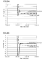
- FIGS. 9A and 9B are diagrams of the simulation results of the semiconductor inspection apparatus according to the present embodiment.
- FIG. 9A illustrates the time variation in each of the drain voltage and the detection voltage of the present embodiment.
- FIG. 9B illustrates the time variation in each of the drain voltage and the detection voltage of the first embodiment.
- the present embodiment can provide a semiconductor inspection apparatus that can evaluate the current collapse from a shorter period of time after the switching.
- the semiconductor inspection apparatus is similar to the semiconductor inspection apparatus of the second embodiment except that a second diode is a Zener diode. Thus, the descriptions of the contents overlapping with the second embodiment may be omitted.
- FIG. 10 is a circuit diagram of the semiconductor inspection apparatus according to the present embodiment.
- the semiconductor inspection apparatus according to the present embodiment includes a second diode 38.
- the second diode 38 is a Zener diode.
- the drain voltage Vd increases to the test voltage V 2 .
- the voltage of a second detecting unit 14 increases to a high voltage due to the parasitic capacitance of the first diode 16. This may unfortunately cause unstable operation of the semiconductor inspection apparatus.
- Zener diode As the second diode 38 can prevent the voltage of the second detecting unit 14 from increasing to the Zener voltage or more. This can achieve stable operation of the semiconductor inspection apparatus.
- the Zener voltage is set at a higher voltage than a first voltage V 1 by between 1 and 5 V.
- the present embodiment can provide a semiconductor inspection apparatus that can evaluate the current collapse from a shorter period of time after the switching. Furthermore, stable operation of the semiconductor inspection apparatus can be achieved.
- the semiconductor inspection apparatus is similar to the semiconductor inspection apparatus of the third embodiment except for further including a first capacitor electrically connected in parallel with a first diode and a second capacitor electrically connected in parallel with a second diode.
- a first capacitor electrically connected in parallel with a first diode
- a second capacitor electrically connected in parallel with a second diode.
- FIG. 11 is a circuit diagram of the semiconductor inspection apparatus according to the present embodiment.
- the semiconductor inspection apparatus according to the present embodiment includes a first capacitor 40 electrically connected to a first diode 16 in parallel and a second capacitor 42 electrically connected to a second diode 38 in parallel.
- adjusting the capacitance of the first capacitor 40 and the capacitance of the second capacitor 42 can further prevent the detection voltage from dropping toward a negative value just after the switching of the HEMT 10.
- the variation in drain voltage Vd can be observed from an even shorter period of time after the switching.
- the present embodiment can provide a semiconductor inspection apparatus that can evaluate the current collapse from an even shorter period of time after the switching.
- adding only one of the first capacitor 40 and the second capacitor 42 and regulating the capacitance can also reduce the drop of the detection voltage toward a negative value just after the switching of the HEMT 10.
- the semiconductor inspection apparatus includes an inductive load on the side of a drain electrode.
- the descriptions of the contents overlapping with the third embodiment may be omitted.
- FIG. 12 is a circuit diagram of the semiconductor inspection apparatus according to the present embodiment.
- the semiconductor inspection apparatus according to the present embodiment includes an inductive load 44 working as a load and formed by a coil and a diode electrically connected to each other in parallel on the side of a drain electrode 10b.
- a current probe 46 is connected between a source electrode 10a and a ground potential.
- using the inductive load 44 as a load can evaluate current collapse in a double pulse test approximate to practical conditions.
- the HEMT of a GaN based semiconductor has been described above as an exemplary field effect transistor in the embodiments.
- the embodiments can be applied to field effect transistors other than the HEMT to evaluate the variation in on-resistance just after the field effect transistor is switched.
Landscapes
- Engineering & Computer Science (AREA)
- Microelectronics & Electronic Packaging (AREA)
- Physics & Mathematics (AREA)
- General Physics & Mathematics (AREA)
- Testing Of Individual Semiconductor Devices (AREA)
- Junction Field-Effect Transistors (AREA)
Description
- This application is based upon and claims the benefit of priority from Japanese Patent Application No.
2014-181653, filed on September 5, 2014 - Embodiments described herein relate generally to a semiconductor inspection apparatus.
- Group III nitride semiconductor, for example, a gallium nitride (GaN) based semiconductor is expected to be used as a material for next-generation semiconductor devices. The GaN based semiconductor device includes a wider bandgap than that of a silicon (Si) semiconductor device, and thus can achieve a high breakdown voltage and a low loss in comparison to the Si semiconductor device.
- A High Electron Mobility Transistor (HEMT) structure using a two-dimensional electron gas (2DEG) as the carrier is widely applied to a field effect transistor using a GaN based semiconductor. Unfortunately, a phenomenon called current collapse occurs in a field effect transistor having such an HEMT structure.
- The current collapse is a phenomenon that the application of high drain voltage to a field effect transistor results in increase of on-resistance. To predict the influence of the current collapse on a circuit configured to operate at a high frequency, it is preferable to evaluate the current collapse occurring just after the switching of the field effect transistor.
-
-
FIG. 1 is a circuit diagram of the semiconductor inspection apparatus according to a first embodiment; -
FIGS. 2A and 2B are explanatory diagrams of the semiconductor inspection apparatus according to a first comparative embodiment; -
FIG. 3 is a diagram of the characteristics of drain voltage and drain current of a field effect transistor; -
FIGS. 4A and 4B are explanatory diagrams of the semiconductor inspection apparatus according to a second comparative embodiment; -
FIGS. 5A and 5B are explanatory diagrams of the function of the semiconductor inspection apparatus according to the first embodiment; -
FIGS. 6A and 6B are diagrams of the simulation results of the semiconductor inspection apparatus according to the first embodiment; -
FIG. 7 is a diagram of the measurement results of the on-resistance by the semiconductor inspection apparatus according to the first embodiment; -
FIG. 8 is a circuit diagram of the semiconductor inspection apparatus according to a second embodiment; -
FIGS. 9A and 9B are diagrams of the simulation results of the semiconductor inspection apparatus according to the second embodiment; -
FIG. 10 is a circuit diagram of the semiconductor inspection apparatus according to a third embodiment; -
FIG. 11 is a circuit diagram of the semiconductor inspection apparatus according to a fourth embodiment; and -
FIG. 12 is a circuit diagram of the semiconductor inspection apparatus according to a fifth embodiment. - The semiconductor inspection apparatus according to an embodiment includes a first detecting unit capable of being electrically connected to a source electrode of a field effect transistor to be evaluated, the first detecting unit used for detecting voltage; a first diode including a first anode electrode and a first cathode electrode, the first cathode electrode capable of being electrically connected to a drain electrode of the field effect transistor; a second detecting unit electrically connected to the first anode electrode, the second detecting unit used for detecting voltage; a first resistance element of which a first end is electrically connected to the first anode electrode; and a first electric power source electrically connected to a second end of the first resistance element.
- The embodiments of the present disclosure will be described with reference to the appended drawings. Note that, in the description below, the same components and the like are denoted with the same reference signs and the descriptions of the components and the like that have been described are appropriately omitted.
- Herein, semiconductors including gallium nitride (GaN), aluminum nitride (AlN), indium nitride (InN), and their intermediate compositions are collectively referred to as a "GaN based semiconductor".
- A semiconductor inspection apparatus of the present embodiment includes: a first detecting unit capable of being electrically connected to a source electrode of a field effect transistor to be evaluated, the first detecting unit used for detecting voltage; a first diode including a first anode electrode and a first cathode electrode, the first cathode electrode capable of being electrically connected to a drain electrode of the field effect transistor; a second detecting unit electrically connected to the first anode electrode, the second detecting unit used for detecting voltage; a first resistance element of which a first end is electrically connected to the first anode electrode; and a first electric power source electrically connected to a second end of the first resistance element.
-
FIG. 1 is a circuit diagram of the semiconductor inspection apparatus according to the present embodiment. The semiconductor inspection apparatus of the present embodiment is configured to inspect anHEMT 10 of a GaN based semiconductor. The HEMT of the GaN based semiconductor is an exemplary field effect transistor. The HEMT 10 includes asource electrode 10a, adrain electrode 10b, and agate electrode 10c. The semiconductor inspection apparatus according to the present embodiment is configured to evaluate the current collapse in theHEMT 10. - The semiconductor inspection apparatus according to the present embodiment includes a first detecting
unit 12, a second detectingunit 14, afirst diode 16, a first resistance element (first electric resistance) 18, a firstelectric power source 20, a second resistance element (second electric resistance) 22, a secondelectric power source 24, agate drive circuit 26, and ameasuring instrument 28. - The
first diode 16 includes afirst anode electrode 16a and afirst cathode electrode 16b. Thefirst cathode electrode 16b of thefirst diode 16 is electrically connected to thedrain electrode 10b of the HEMT 10. A first end of thefirst resistance element 18 is electrically connected to thefirst anode electrode 16a of thefirst diode 16. A second end of thefirst resistance element 18 is electrically connected to the firstelectric power source 20. - The first detecting
unit 12 is electrically connected to thesource electrode 10a of the HEMT 10. In the present embodiment, the first detectingunit 12 and thesource electrode 10a are fixed at ground potentials, respectively. The second detectingunit 14 is electrically connected to thefirst anode electrode 16a of thefirst diode 16. - A first end of the
second resistance element 22 is electrically connected to thedrain electrode 10b of the HEMT 10. A second end of thesecond resistance element 22 is electrically connected to the secondelectric power source 24. - The
gate drive circuit 26 is electrically connected to thegate electrode 10c of the HEMT 10. Themeasuring instrument 28 is electrically connected to the first detectingunit 12 and the second detectingunit 14. - The HEMT 10 to be inspected is, for example, formed on a semiconductor wafer and is electrically connected to the semiconductor inspection apparatus through a probe.
- The HEMT 10 is implemented, for example, in a package and is electrically connected to the semiconductor inspection apparatus through a socket.
- The second
electric power source 24 is electrically connected to thedrain electrode 10b while thesecond resistance element 22 working as a load is held therebetween. The secondelectric power source 24 applies a test voltage V2 to thedrain electrode 10b. The test voltage V2 is, for example, between 100 and 500 V. The secondelectric power source 24 is, for example, a power circuit. - The
gate drive circuit 26 controls a gate voltage to be applied to thegate electrode 10c of theHEMT 10. Thegate drive circuit 26 controls the on and off of the HEMT 10. Thegate drive circuit 26 includes, for example, a pulsevoltage generation circuit 30 and aresistance element 32. The gate voltage is, for example, 0 V when theHEMT 10 is off, and between 5 and 30 V when the HEMT 10 is on. - When the
HEMT 10 is on, a drain current flows due to the drain voltage applied between thesource electrode 10a and thedrain electrode 10b. Hereinafter, the drain voltage of theHEMT 10 is denoted with Vd and the drain current is denoted with Id. - When the
HEMT 10 is off, the drain voltage Vd is a high voltage equivalent to the test voltage V2. Thefirst diode 16 has a function of blocking a high voltage from being applied to the second detectingunit 14 when theHEMT 10 is off. - The breakdown voltage of the
first diode 16 is higher than the drain voltage Vd applied to thedrain electrode 10b of theHEMT 10. In other words, the breakdown voltage of thefirst diode 16 is higher than the test voltage V2. - Hereinafter, the forward voltage drop is denoted with Vf. The
first diode 16 is, for example, a pn diode made of silicon (Si). - The first
electric power source 20 has a function of charging thefirst anode electrode 16a of thefirst diode 16 when theHEMT 10 is on. The firstelectric power source 20 is, for example, a power circuit. - The voltage of the first
electric power source 20 is lower than the test voltage V2 that the secondelectric power source 24 applies to thedrain electrode 10b. In other words, the test voltage V2 that the secondelectric power source 24 applies to thedrain electrode 10b is higher than the voltage of the firstelectric power source 20. - The setting for the voltage of the first
electric power source 20 is configured to be a higher voltage than the drain voltage Vd when theHEMT 10 is on. Hereinafter, the voltage of the firstelectric power source 20 is denoted with V1. The voltage V1 of the firstelectric power source 20 is, for example, between 5 and 30 V. - When the
first diode 16 is charged while theHEMT 10 is on, thefirst resistance element 18 determines the current that flows from the firstelectric power source 20 to thefirst diode 16. A relationship of R1 ≥ 10V1/Id is preferably satisfied when the resistance value of the first resistance element is R1. - The drain voltage Vd of the
HEMT 10 may indirectly be measured with the first detectingunit 12 and the second detectingunit 14. Each of the first detectingunit 12 and the second detectingunit 14 is, for example, an electric terminal to which a probe electrically connected to the measuringinstrument 28 may be connected. - Note that each of the first detecting
unit 12 and the second detectingunit 14 needs only to be a portion at the same potential as that of thesource electrode 10a of theHEMT 10 and thefirst anode electrode 16a of thefirst diode 16. Each of the first detectingunit 12 and the second detectingunit 14 is not necessarily an independent unit such as an electric terminal. Each of the first detectingunit 12 and the second detectingunit 14 may, for example, be a part of electric wiring. - The measuring
instrument 28 has a function of measuring the voltage between the first detectingunit 12 and the second detectingunit 14. The measuringinstrument 28 is, for example, an oscilloscope. The measuringinstrument 28 is, for example, electrically connected to the first detectingunit 12 and the second detectingunit 14 through a probe. The measuringinstrument 28 may directly be connected to the first detectingunit 12 and the second detectingunit 14, for example, by electric wiring. - Next, an inspection method using the semiconductor inspection apparatus according to the present embodiment will be described.
- First, the
HEMT 10 of the GaN based semiconductor of which current collapse is to be evaluated is prepared. The initial on-resistance of theHEMT 10 before the application of the test voltage is previously and separately found by measurement. Furthermore, a forward voltage drop Vf of thefirst diode 16 is previously and separately found. - Next, the
source electrode 10a, thedrain electrode 10b, and thegate electrode 10c of theHEMT 10 are electrically connected to the semiconductor inspection apparatus. The method for connection is not especially limited. A method in which the electrodes are inserted in sockets or a method in which probes have contact with the electrodes may be used according to the aspect of theHEMT 10. - Next, while 0 V is applied to the
gate electrode 10c with thegate drive circuit 26 and theHEMT 10 is off, the test voltage V2 is applied to thedrain electrode 10b with the secondelectric power source 24. At that time, the voltage V1 lower than the test voltage V2 is applied to thefirst anode electrode 16a of thefirst diode 16 with the firstelectric power source 20. - Next, a positive voltage is applied to the
gate electrode 10c with thegate drive circuit 26 and theHEMT 10 is switched to on. Furthermore, theHEMT 10 may continuously be switched to repeat on and off. - When the
HEMT 10 is switched, the voltage between the first detectingunit 12 and the second detectingunit 14 is measured with the measuringinstrument 28. The voltage between the first detectingunit 12 and the second detectingunit 14 is the sum of the drain voltage Vd and the forward voltage drop Vf of thefirst diode 16 when theHEMT 10 is on. Thus, taking the difference between the measured voltage and the forward voltage drop Vf can find the drain voltage Vd. - The drain current Id may be found, for example, from the resistance value of the
second resistance element 22, and the difference between the test voltage V2 and the drain voltage Vd, with Ohm's law. Alternatively, the drain current Id may directly be measured, for example, by insertion of a sense resistor, or with a current probe. - From the drain voltage Vd the drain current Id when the
HEMT 10 is on, the on-resistance of theHEMT 10 after the application of the test voltage V2 may be found. The comparison between the on-resistance after the application of the test voltage V2 and the initial on-resistance may find the increment of the on-resistance due to the current collapse. - Next, the functions and effects of the semiconductor inspection apparatus according to the present embodiment will be described.
-
FIGS. 2A and 2B are explanatory diagrams of the semiconductor inspection apparatus according to a first comparative embodiment.FIG. 2A is a circuit diagram, andFIG. 2B is a diagram of the time variation in detection voltage. - Differently from the present first embodiment, the first comparative embodiment does not include a
first diode 16, afirst resistance element 18, and a firstelectric power source 20. The first comparative embodiment directly measures the drain voltage Vd by measuring a voltage (detection voltage) between a first detectingunit 12 and a second detectingunit 14. - As illustrated in
FIG. 2B , the detection voltage is a high test voltage V2, for example, of hundreds of volts when theHEMT 10 is off. On the other hand, the detection voltage is a low voltage, for example, of several volts as a result from the resistive division of the on-resistance of theHEMT 10 and thesecond resistance element 22 working as a load when theHEMT 10 is on. - Thus, for example, setting the measurement range of the oscilloscope, which is an example of the measuring
instrument 28, at a range appropriate to the test voltage V2 makes it difficult to measure the drain voltage Vd due to the SN ratio and/or the resolution. In contrast, setting the measurement range of the oscilloscope at a range appropriate to the drain voltage Vd when theHEMT 10 is on makes it difficult to measure the drain voltage Vd accurately because of the saturation of the oscilloscope and/or the saturation of the probe connecting the oscilloscope to the first detectingunit 12 and the second detectingunit 14. -
FIG. 3 is a diagram of the characteristics of the drain voltage and drain current of a field effect transistor. For example, to evaluate the circuit operation of a power circuit using the field effect transistor as a switching device, the measurement of characteristics of the field effect transistor in a linear region is required. - For example, one method to avoid the problem caused by the SN ratio and/or the resolution in the first comparative embodiment is to set the resistance value of the
second resistance element 22 to make the drain voltage Vd high when theHEMT 10 is on. However, such setting causes a problem that the current collapse of theHEMT 10 in the linear region is not evaluated. -
FIGS. 4A and 4B are explanatory diagrams of the semiconductor inspection apparatus according to a second comparative embodiment.FIG. 4A is a circuit diagram, andFIG. 4B is a diagram of the time variation in detection voltage. - The second comparative embodiment is further provided with a
resistance element 34 and aresistance element 36 in addition to the first comparative embodiment. Providing theresistance element 34 andresistance element 36 of high-resistance can reduce the detection voltage when theHEMT 10 is off, using the effect of resistive division. This makes it possible to avoid the problem caused by the SN ratio and/or the resolution. - However, when a circuit such as a DC/DC converter of which operation frequency is assumed to be one megahertz or higher is used, it is necessary to detect the current collapse from tens of nanoseconds after the switching of the field effect transistor.
- A CR delay due to the
resistance element 34 andresistance element 36 of high resistance and/or the parasitic capacitance of the probe occurs in the second comparative embodiment. Thus, the waveform just after the switching of theHEMT 10 from off-state to on-state is rounded off, as illustrated inFIG. 4B . The waveform of the detection voltage when current collapse occurs shows a similar movement. Thus, it may be impossible to distinguish the variation in detection voltage due to the CR delay from the variation in detection voltage due to the current collapse. This makes it difficult to observe and evaluate the current collapse just after the switching. -
FIGS. 5A and 5B are explanatory diagrams of the function of the semiconductor inspection apparatus according to the present first embodiment.FIG. 5A is a circuit diagram, andFIG. 5B is a diagram of the time variation in detection voltage. - In the present embodiment, the test voltage V2 is blocked by the
first diode 16 when theHEMT 10 is off. Thus, the detection voltage when theHEMT 10 is off is the voltage V1 applied by the firstelectric power source 20. The voltage V1 is set at a lower value than the test voltage V2. - When the
HEMT 10 is switched from off-state to on-state, a drain current starts flowing and the drain voltage Vd decreases. This causes charge extraction due to a parasitic capacitance Cp1 of thefirst diode 16 in a time range A inFIG. 5B and the detection voltage also decreases. Subsequently, a parasitic capacitance Cp2 between the first detectingunit 12 and the second detectingunit 14 is charged from the firstelectric power source 20 through thefirst resistance element 18 in a time range B. This increases the detection voltage. - A higher voltage of the second detecting
unit 14 than the drain voltage Vd causes a forward current to flow in thefirst diode 16. The detection voltage in such a state is the sum of the drain voltage Vd and the forward voltage drop Vf of thefirst diode 16. - According to the semiconductor inspection apparatus of the present embodiment, the detection voltage when the
HEMT 10 is off is the voltage V1 lower than the test voltage V2. As a result, the difference of the detection voltages when theHEMT 10 is off-state and on-state decreases. This solves the problem caused by the SN ratio or the resolution. The increase in drain voltage Vd is not required. Thus, the current collapse in the linear region may be observed and evaluated. - Furthermore, the movement of the observed waveform just after the switching of the
HEMT 10 can be opposite to the movement when current collapse occurs. This makes it easy to observe the on-resistance just after the switching called dynamic on-resistance. Thus, the current collapse can accurately be evaluated just after the switching. - Furthermore, the parasitic capacitance can be decreased in comparison to the second comparative embodiment. This suppress the CR delay. This also enables the current collapse to be evaluated accurately just after the switching.
-
FIGS. 6A and 6B are diagrams of the simulation results of the semiconductor inspection apparatus according to the present embodiment.FIG. 6A illustrates the time variation in each of the gate voltage, the drain voltage, and the detection voltage.FIG. 6B is an enlarged view of a region just after the switching illustrated inFIG. 6A , and illustrates the drain voltage and the detection voltage. - When the gate voltage is zero V while the
HEMT 10 is off, the drain voltage Vd is a high voltage (400 V) whereas the detection voltage is maintained at the voltage V1 (10 V) of the firstelectric power source 20. The gate voltage changes from zero V to a positive voltage (15 V) and theHEMT 10 is on. When theHEMT 10 is on, the detection voltage temporarily drops from zero V and then increases. - When a forward current flows in the
first diode 16, the detection voltage is the sum of the drain voltage Vd and the forward voltage drop Vf of thefirst diode 16, as illustrated inFIG. 6B . In other words, the difference between the detection voltage and the drain voltage Vd is the forward voltage drop Vf. -
FIG. 7 is a diagram of the measurement results of the on-resistance by the semiconductor inspection apparatus according to the present embodiment, and illustrates the time variation in on-resistance. The time elapsed after a positive voltage is applied to the gate voltage and theHEMT 10 is switched to on is shown on the horizontal axis. - As illustrated in
FIG. 7 , the on-resistance can be measured from a short time of 20 nanoseconds after theHEMT 10 is switched. - As described above, the present embodiment can provide a semiconductor inspection apparatus that can evaluate the current collapse from a short period of time after the switching.
- Note that a relationship of R1 ≥ 10V1/Id is preferably satisfied when the drain current of the field effect transistor is Id, the voltage of the first
electric power source 20 is V1, and the resistance value of thefirst resistance element 18 is R1. Satisfying the relationship makes the current flowing from thefirst diode 16 toward thedrain electrode 10b when theHEMT 10 is on equal to or less than a tenth of the drain current Id. This can suppress the influence of the current flowing from thefirst diode 16 toward thedrain electrode 10b on the measurement of the drain voltage Vd. Furthermore, in terms of the reduction in influence, a relationship of R1 ≥ 100V1/Id is more preferably satisfied. - Note that the
first diode 16 is preferably a fast recovery diode. The fast recovery diode has an excellent recovery characteristic, and thus can accelerate the evaluation especially when theHEMT 10 is continuously switched. - The
first diode 16 is also preferably a Schottky barrier diode made of SiC. The Schottky barrier diode made of SiC has an excellent temperature characteristic, and thus improves the accuracy of measurement of a voltage. - The Schottky barrier diode made of SiC has also an excellent recovery characteristic, and thus can accelerate the evaluation especially when the
HEMT 10 is continuously switched. - An exemplary aspect in which the semiconductor inspection apparatus includes the
second resistance element 22, the secondelectric power source 24, thegate drive circuit 26, and the measuringinstrument 28 is described in the present embodiment. Note that, however, the semiconductor inspection apparatus can also include the components outside the inspection apparatus. For example,
a semiconductor inspection apparatus configured to evaluate current collapse may include the first detectingunit 12, the second detectingunit 14, thefirst diode 16, thefirst resistance element 18, and the firstelectric power source 20. A transistor evaluation system may include components corresponding to thesecond resistance element 22, the secondelectric power source 24, and thegate drive circuit 26. The semiconductor inspection apparatus may be connected to the transistor evaluation system. Additionally, the measuringinstrument 28 may be externally connected to the first detectingunit 12 and the second detectingunit 14. - The semiconductor inspection apparatus according to the present embodiment is similar to the semiconductor inspection apparatus of the first embodiment except for further including a second diode including a second anode electrode electrically connected to a first detecting unit and a second cathode electrode electrically connected to a second detecting unit. Thus, the descriptions of the contents overlapping with the first embodiment may be omitted.
-
FIG. 8 is a circuit diagram of the semiconductor inspection apparatus according to the present embodiment. The semiconductor inspection apparatus according to the present embodiment includes asecond diode 38. Thesecond diode 38 includes asecond anode electrode 38a and asecond cathode electrode 38b. - The
second anode electrode 38a is electrically connected to a first detectingunit 12. Thesecond cathode electrode 38b is electrically connected to a second detectingunit 14. Thesecond diode 38 is, for example, a pn diode. - The
second diode 38 prevents the detection voltage from excessively dropping toward a negative value just after anHEMT 10 is switched. This enables the second embodiment to observe and evaluate current collapse from a shorter period of time after the switching. -
FIGS. 9A and 9B are diagrams of the simulation results of the semiconductor inspection apparatus according to the present embodiment.FIG. 9A illustrates the time variation in each of the drain voltage and the detection voltage of the present embodiment.FIG. 9B illustrates the time variation in each of the drain voltage and the detection voltage of the first embodiment. - As is clear from the comparison between
FIGS. 9A and 9B , the drop of the detection voltage toward a negative value just after the switching of theHEMT 10 is suppressed in the present embodiment. As a result, the variation in drain voltage Vd can be observed from a shorter period of time after the switching. - As described above, the present embodiment can provide a semiconductor inspection apparatus that can evaluate the current collapse from a shorter period of time after the switching.
- The semiconductor inspection apparatus according to the present embodiment is similar to the semiconductor inspection apparatus of the second embodiment except that a second diode is a Zener diode. Thus, the descriptions of the contents overlapping with the second embodiment may be omitted.
-
FIG. 10 is a circuit diagram of the semiconductor inspection apparatus according to the present embodiment. The semiconductor inspection apparatus according to the present embodiment includes asecond diode 38. Thesecond diode 38 is a Zener diode. - For example, when the
HEMT 10 is continuously switched and then theHEMT 10 is off, the drain voltage Vd increases to the test voltage V2. At that time, the voltage of a second detectingunit 14 increases to a high voltage due to the parasitic capacitance of thefirst diode 16. This may unfortunately cause unstable operation of the semiconductor inspection apparatus. - When a constant voltage (Zener voltage) is applied in a reverse direction, a current flows in the reverse direction in the Zener diode due to Avalanche breakdown. Thus, using a Zener diode as the
second diode 38 can prevent the voltage of the second detectingunit 14 from increasing to the Zener voltage or more. This can achieve stable operation of the semiconductor inspection apparatus. - For example, the Zener voltage is set at a higher voltage than a first voltage V1 by between 1 and 5 V.
- As described above, the present embodiment can provide a semiconductor inspection apparatus that can evaluate the current collapse from a shorter period of time after the switching. Furthermore, stable operation of the semiconductor inspection apparatus can be achieved.
- The semiconductor inspection apparatus according to the present embodiment is similar to the semiconductor inspection apparatus of the third embodiment except for further including a first capacitor electrically connected in parallel with a first diode and a second capacitor electrically connected in parallel with a second diode. Thus, the descriptions of the contents overlapping with the third embodiment may be omitted.
-
FIG. 11 is a circuit diagram of the semiconductor inspection apparatus according to the present embodiment. The semiconductor inspection apparatus according to the present embodiment includes afirst capacitor 40 electrically connected to afirst diode 16 in parallel and asecond capacitor 42 electrically connected to asecond diode 38 in parallel. - According to the present embodiment, adjusting the capacitance of the
first capacitor 40 and the capacitance of thesecond capacitor 42 can further prevent the detection voltage from dropping toward a negative value just after the switching of theHEMT 10. Thus, the variation in drain voltage Vd can be observed from an even shorter period of time after the switching. - As described above, the present embodiment can provide a semiconductor inspection apparatus that can evaluate the current collapse from an even shorter period of time after the switching.
- Note that adding only one of the
first capacitor 40 and thesecond capacitor 42 and regulating the capacitance can also reduce the drop of the detection voltage toward a negative value just after the switching of theHEMT 10. - Differently from the third embodiment, the semiconductor inspection apparatus according to the present embodiment includes an inductive load on the side of a drain electrode. The descriptions of the contents overlapping with the third embodiment may be omitted.
-
FIG. 12 is a circuit diagram of the semiconductor inspection apparatus according to the present embodiment. The semiconductor inspection apparatus according to the present embodiment includes aninductive load 44 working as a load and formed by a coil and a diode electrically connected to each other in parallel on the side of adrain electrode 10b. Acurrent probe 46 is connected between asource electrode 10a and a ground potential. - According to the present embodiment, using the
inductive load 44 as a load can evaluate current collapse in a double pulse test approximate to practical conditions. - The HEMT of a GaN based semiconductor has been described above as an exemplary field effect transistor in the embodiments. The embodiments, however, can be applied to field effect transistors other than the HEMT to evaluate the variation in on-resistance just after the field effect transistor is switched.
- While certain embodiments have been described, these embodiments have been presented by way of example only, and are not intended to limit the scope of the inventions. Indeed, the semiconductor device inspection apparatus described herein may be embodied in a variety of other forms; furthermore, various omissions, substitutions and changes in the form of the devices and methods described herein may be made without departing from the spirit of the inventions. The accompanying claims and their equivalents are intended to cover such forms or modifications as would fall within the scope and spirit of the inventions.
Claims (12)
- A semiconductor inspection apparatus comprising:a first detecting unit capable of being electrically connected to a source electrode of a field effect transistor to be evaluated, the first detecting unit used for detecting voltage;a first diode including a first anode electrode and a first cathode electrode, the first cathode electrode capable of being electrically connected to a drain electrode of the field effect transistor;a second detecting unit electrically connected to the first anode electrode, the second detecting unit used for detecting voltage;a first resistance element of which a first end is electrically connected to the first anode electrode; anda first electric power source electrically connected to a second end of the first resistance element.
- The apparatus according to claim 1, wherein a breakdown voltage of the first diode is higher than a drain voltage to be applied to the drain electrode.
- The apparatus according to claim 1, wherein a relationship of R1 ≥ 10V1/Id is satisfied, where R1 is a resistance value of the first resistance element, V1 is a voltage of the first electric power source and Id is a drain current of the field effect transistor.
- The apparatus according to claim 1, further comprising:a second diode including a second anode electrode and a second cathode electrode, the second anode electrode electrically connected to the first detecting unit, the second cathode electrode electrically connected to the second detecting unit.
- The apparatus according to claim 4, wherein the second diode is a Zener diode.
- The apparatus according to claim 1, further comprising:a second resistance element of which a first end is capable of being electrically connected to the drain electrode; anda second electric power source electrically connected to a second end of the second resistance element, the second electric power source applying a voltage higher than a voltage of the first electric power source.
- The apparatus according to claim 1, wherein the first diode is a fast recovery diode.
- The apparatus according to claim 1, wherein the first diode is a Schottky barrier diode including SiC.
- The apparatus according to claim 4, further comprising:a first capacitor electrically connected in parallel with the first diode; anda second capacitor electrically connected in parallel with the second diode.
- The apparatus according to claim 1, further comprising:a gate drive circuit capable of being electrically connected to a gate electrode of the field effect transistor.
- The apparatus according to claim 1, further comprising:a measuring instrument electrically connected to the first detecting unit and the second detecting unit, the measuring instrument measuring a voltage between the first detecting unit and the second detecting unit.
- The apparatus according to claim 1, wherein the field effect transistor is an HEMT of a GaN based semiconductor.
Applications Claiming Priority (1)
| Application Number | Priority Date | Filing Date | Title |
|---|---|---|---|
| JP2014181653A JP6293623B2 (en) | 2014-09-05 | 2014-09-05 | Semiconductor inspection equipment |
Publications (2)
| Publication Number | Publication Date |
|---|---|
| EP2995965A1 true EP2995965A1 (en) | 2016-03-16 |
| EP2995965B1 EP2995965B1 (en) | 2017-10-04 |
Family
ID=53496580
Family Applications (1)
| Application Number | Title | Priority Date | Filing Date |
|---|---|---|---|
| EP15174843.1A Active EP2995965B1 (en) | 2014-09-05 | 2015-07-01 | Semiconductor inspection apparatus |
Country Status (3)
| Country | Link |
|---|---|
| US (1) | US9778311B2 (en) |
| EP (1) | EP2995965B1 (en) |
| JP (1) | JP6293623B2 (en) |
Families Citing this family (14)
| Publication number | Priority date | Publication date | Assignee | Title |
|---|---|---|---|---|
| US10094863B2 (en) * | 2016-03-02 | 2018-10-09 | Texas Instruments Incorporated | High-resolution power electronics measurements |
| US9970980B2 (en) * | 2016-08-26 | 2018-05-15 | Infineon Technologies Ag | Test circuit for stress leakage measurements |
| US10317428B2 (en) * | 2016-11-02 | 2019-06-11 | Intel Corporation | Probe connector for a probing pad structure around a thermal attach mounting hole |
| EP3581949A4 (en) | 2017-02-08 | 2020-02-12 | Nec Corporation | HIGH FREQUENCY MEASUREMENT METHOD AND DEVICE |
| JP7108386B2 (en) * | 2017-08-24 | 2022-07-28 | 住友化学株式会社 | Charge trap evaluation method |
| US11067620B2 (en) * | 2018-08-21 | 2021-07-20 | Texas Instruments Incorporated | HEMT wafer probe current collapse screening |
| CN111426928B (en) * | 2018-12-24 | 2021-08-20 | 东南大学 | A dynamic resistance test circuit of gallium nitride device |
| CN110579698A (en) * | 2019-09-10 | 2019-12-17 | 江南大学 | A method for testing junction temperature of InAlN/GaN HEMT |
| US11448686B2 (en) * | 2019-09-18 | 2022-09-20 | Texas Instruments Incorporated | RDSON/dRON measurement method and circuit for high voltage HEMTs |
| CN111289799B (en) * | 2020-03-03 | 2021-01-08 | 电子科技大学 | GaN device dynamic on-resistance measuring circuit |
| CN113533923A (en) * | 2021-06-17 | 2021-10-22 | 深圳天狼芯半导体有限公司 | GaN HEMT device testing method and device |
| CN114646809B (en) * | 2022-03-30 | 2025-09-23 | 北京华峰测控技术股份有限公司 | A test circuit and test method for dynamic resistance of gallium nitride power device |
| CN116298766B (en) * | 2023-05-16 | 2023-08-01 | 成都思科瑞微电子股份有限公司 | Test method of insulated gate field effect transistor |
| JP2025042976A (en) * | 2023-09-15 | 2025-03-28 | 株式会社東芝 | Inspection device, inspection system, inspection method, and manufacturing method of semiconductor device |
Citations (3)
| Publication number | Priority date | Publication date | Assignee | Title |
|---|---|---|---|---|
| US20070013407A1 (en) * | 2005-06-16 | 2007-01-18 | Agilent Technologies, Inc. | Method for measuring FET characteristics |
| US20110249476A1 (en) * | 2010-04-07 | 2011-10-13 | Richpower Microelectronics Corporation | Voltage detector and protection apparatus using the same |
| US20140139206A1 (en) * | 2012-11-22 | 2014-05-22 | Fujitsu Limited | Voltage detecting circuit and method for measuring characteristic of transistor |
Family Cites Families (15)
| Publication number | Priority date | Publication date | Assignee | Title |
|---|---|---|---|---|
| JPH051828Y2 (en) * | 1985-11-08 | 1993-01-18 | ||
| US4851769A (en) * | 1988-04-11 | 1989-07-25 | Virginia Tech Intellectual Properties, Inc. | Non-destructive tester for transistors |
| US5041960A (en) * | 1990-02-20 | 1991-08-20 | Yefim Tseruel | Frequency doubler and/or self-oscillating inverter |
| JPH03293818A (en) * | 1990-03-02 | 1991-12-25 | Ricoh Co Ltd | AD conversion device |
| JP3090518B2 (en) * | 1991-12-06 | 2000-09-25 | フィガロ技研株式会社 | Air conditioning control device |
| JP2011204877A (en) * | 2010-03-25 | 2011-10-13 | Panasonic Corp | Field-effect transistor and method of evaluating the same |
| US8773031B2 (en) * | 2010-11-22 | 2014-07-08 | Innosys, Inc. | Dimmable timer-based LED power supply |
| JP2012181051A (en) | 2011-02-28 | 2012-09-20 | Panasonic Corp | Diode device and diode device evaluation method |
| JP2013015416A (en) | 2011-07-04 | 2013-01-24 | Panasonic Corp | Inspection method of semiconductor element, and semiconductor inspection device |
| WO2013021628A1 (en) * | 2011-08-08 | 2013-02-14 | パナソニック株式会社 | Semiconductor device |
| JP2014225482A (en) * | 2011-09-13 | 2014-12-04 | パナソニック株式会社 | Simulation method and simulation device for semiconductor device |
| JP5288082B1 (en) * | 2011-11-28 | 2013-09-11 | コニカミノルタ株式会社 | Light emitting module |
| TWI477788B (en) * | 2012-04-10 | 2015-03-21 | Realtek Semiconductor Corp | Apparatus and method of led short detection |
| JP2014119379A (en) * | 2012-12-18 | 2014-06-30 | Sharp Corp | Test method for semiconductor transistor |
| JP6432201B2 (en) * | 2014-03-17 | 2018-12-05 | 富士電機株式会社 | Semiconductor device and manufacturing method of semiconductor device |
-
2014
- 2014-09-05 JP JP2014181653A patent/JP6293623B2/en active Active
-
2015
- 2015-07-01 EP EP15174843.1A patent/EP2995965B1/en active Active
- 2015-07-23 US US14/807,335 patent/US9778311B2/en active Active
Patent Citations (3)
| Publication number | Priority date | Publication date | Assignee | Title |
|---|---|---|---|---|
| US20070013407A1 (en) * | 2005-06-16 | 2007-01-18 | Agilent Technologies, Inc. | Method for measuring FET characteristics |
| US20110249476A1 (en) * | 2010-04-07 | 2011-10-13 | Richpower Microelectronics Corporation | Voltage detector and protection apparatus using the same |
| US20140139206A1 (en) * | 2012-11-22 | 2014-05-22 | Fujitsu Limited | Voltage detecting circuit and method for measuring characteristic of transistor |
Also Published As
| Publication number | Publication date |
|---|---|
| EP2995965B1 (en) | 2017-10-04 |
| US20160069946A1 (en) | 2016-03-10 |
| US9778311B2 (en) | 2017-10-03 |
| JP2016057091A (en) | 2016-04-21 |
| JP6293623B2 (en) | 2018-03-14 |
Similar Documents
| Publication | Publication Date | Title |
|---|---|---|
| EP2995965B1 (en) | Semiconductor inspection apparatus | |
| Badawi et al. | A new method for dynamic Ron extraction of GaN power HEMTs | |
| US9476933B2 (en) | Apparatus and methods for qualifying HEMT FET devices | |
| CN101324639B (en) | Voltage clamp circuit, overcurrent protection circuit, voltage measurement probe, and voltage measurement device | |
| Lagger et al. | Very fast dynamics of threshold voltage drifts in GaN-based MIS-HEMTs | |
| US7501848B2 (en) | Method and apparatus for measuring leakage current | |
| Zhong et al. | Characterization of dynamic threshold voltage in Schottky-type p-GaN gate HEMT under high-frequency switching | |
| CN101728826A (en) | An Input Surge Protection Device Using a Junction Field Effect Transistor | |
| CN110824322B (en) | Apparatus and method for measuring high electron mobility transistors | |
| Meneghesso et al. | Trapping induced parasitic effects in GaN-HEMT for power switching applications | |
| Franke et al. | Advanced temperature estimation in low Rds, on p-GaN HEMT devices for performing power cycling tests | |
| Gelagaev et al. | A novel voltage clamp circuit for the measurement of transistor dynamic on-resistance | |
| Geng et al. | Comparative Analysis of the Characteristics of Schottky-type and Ohmic-type p-GaN Gate GaN HEMTs | |
| de Oliveira et al. | Impact of dynamic on-resistance of high voltage GaN switches on the overall conduction losses | |
| CN112532220A (en) | Semiconductor device with a plurality of semiconductor chips | |
| Marek et al. | Power p-GaN HEMT under unclamped inductive switching conditions | |
| Consentino et al. | Threshold voltage instability in SiC power MOSFETs | |
| CN109522617B (en) | Novel extraction method for degraded average activation energy of AlGaN/GaNHEMT device | |
| EP4249927B1 (en) | Gate oxide deterioration estimation for power semiconductors | |
| Goller et al. | Precise determination of dynamic RDSon in AlGaN/GaN power HEMTs under soft switching condition | |
| Roche et al. | The Decisive Role of Gate Voltage Overshoots on the Dynamic Ron of Schottky p-GaN HEMTs | |
| Everts et al. | A hard switching VIENNA boost converter for characterization of AlGaN/GaN/AlGaN power DHFETs | |
| JP7358227B2 (en) | semiconductor equipment | |
| Li et al. | Measurement of GaN HEMTs’ temperature dependent on-state resistance in switching operation | |
| Reiner et al. | GaN-HEMT with a back-gated segment for high voltage cascodes |
Legal Events
| Date | Code | Title | Description |
|---|---|---|---|
| PUAI | Public reference made under article 153(3) epc to a published international application that has entered the european phase |
Free format text: ORIGINAL CODE: 0009012 |
|
| 17P | Request for examination filed |
Effective date: 20150701 |
|
| AK | Designated contracting states |
Kind code of ref document: A1 Designated state(s): AL AT BE BG CH CY CZ DE DK EE ES FI FR GB GR HR HU IE IS IT LI LT LU LV MC MK MT NL NO PL PT RO RS SE SI SK SM TR |
|
| AX | Request for extension of the european patent |
Extension state: BA ME |
|
| GRAP | Despatch of communication of intention to grant a patent |
Free format text: ORIGINAL CODE: EPIDOSNIGR1 |
|
| STAA | Information on the status of an ep patent application or granted ep patent |
Free format text: STATUS: GRANT OF PATENT IS INTENDED |
|
| RIC1 | Information provided on ipc code assigned before grant |
Ipc: H01L 29/778 20060101ALI20170328BHEP Ipc: H01L 29/20 20060101ALI20170328BHEP Ipc: G01R 31/26 20140101AFI20170328BHEP |
|
| INTG | Intention to grant announced |
Effective date: 20170418 |
|
| RIN1 | Information on inventor provided before grant (corrected) |
Inventor name: IKEDA, KENTARO |
|
| GRAA | (expected) grant |
Free format text: ORIGINAL CODE: 0009210 |
|
| GRAS | Grant fee paid |
Free format text: ORIGINAL CODE: EPIDOSNIGR3 |
|
| STAA | Information on the status of an ep patent application or granted ep patent |
Free format text: STATUS: THE PATENT HAS BEEN GRANTED |
|
| AK | Designated contracting states |
Kind code of ref document: B1 Designated state(s): AL AT BE BG CH CY CZ DE DK EE ES FI FR GB GR HR HU IE IS IT LI LT LU LV MC MK MT NL NO PL PT RO RS SE SI SK SM TR |
|
| REG | Reference to a national code |
Ref country code: GB Ref legal event code: FG4D |
|
| REG | Reference to a national code |
Ref country code: CH Ref legal event code: EP |
|
| REG | Reference to a national code |
Ref country code: AT Ref legal event code: REF Ref document number: 934529 Country of ref document: AT Kind code of ref document: T Effective date: 20171015 |
|
| REG | Reference to a national code |
Ref country code: IE Ref legal event code: FG4D |
|
| REG | Reference to a national code |
Ref country code: DE Ref legal event code: R096 Ref document number: 602015005114 Country of ref document: DE |
|
| REG | Reference to a national code |
Ref country code: NL Ref legal event code: MP Effective date: 20171004 |
|
| REG | Reference to a national code |
Ref country code: LT Ref legal event code: MG4D |
|
| REG | Reference to a national code |
Ref country code: AT Ref legal event code: MK05 Ref document number: 934529 Country of ref document: AT Kind code of ref document: T Effective date: 20171004 |
|
| PG25 | Lapsed in a contracting state [announced via postgrant information from national office to epo] |
Ref country code: NL Free format text: LAPSE BECAUSE OF FAILURE TO SUBMIT A TRANSLATION OF THE DESCRIPTION OR TO PAY THE FEE WITHIN THE PRESCRIBED TIME-LIMIT Effective date: 20171004 |
|
| PG25 | Lapsed in a contracting state [announced via postgrant information from national office to epo] |
Ref country code: NO Free format text: LAPSE BECAUSE OF FAILURE TO SUBMIT A TRANSLATION OF THE DESCRIPTION OR TO PAY THE FEE WITHIN THE PRESCRIBED TIME-LIMIT Effective date: 20180104 Ref country code: SE Free format text: LAPSE BECAUSE OF FAILURE TO SUBMIT A TRANSLATION OF THE DESCRIPTION OR TO PAY THE FEE WITHIN THE PRESCRIBED TIME-LIMIT Effective date: 20171004 Ref country code: FI Free format text: LAPSE BECAUSE OF FAILURE TO SUBMIT A TRANSLATION OF THE DESCRIPTION OR TO PAY THE FEE WITHIN THE PRESCRIBED TIME-LIMIT Effective date: 20171004 Ref country code: ES Free format text: LAPSE BECAUSE OF FAILURE TO SUBMIT A TRANSLATION OF THE DESCRIPTION OR TO PAY THE FEE WITHIN THE PRESCRIBED TIME-LIMIT Effective date: 20171004 Ref country code: LT Free format text: LAPSE BECAUSE OF FAILURE TO SUBMIT A TRANSLATION OF THE DESCRIPTION OR TO PAY THE FEE WITHIN THE PRESCRIBED TIME-LIMIT Effective date: 20171004 |
|
| PG25 | Lapsed in a contracting state [announced via postgrant information from national office to epo] |
Ref country code: BG Free format text: LAPSE BECAUSE OF FAILURE TO SUBMIT A TRANSLATION OF THE DESCRIPTION OR TO PAY THE FEE WITHIN THE PRESCRIBED TIME-LIMIT Effective date: 20180104 Ref country code: GR Free format text: LAPSE BECAUSE OF FAILURE TO SUBMIT A TRANSLATION OF THE DESCRIPTION OR TO PAY THE FEE WITHIN THE PRESCRIBED TIME-LIMIT Effective date: 20180105 Ref country code: IS Free format text: LAPSE BECAUSE OF FAILURE TO SUBMIT A TRANSLATION OF THE DESCRIPTION OR TO PAY THE FEE WITHIN THE PRESCRIBED TIME-LIMIT Effective date: 20180204 Ref country code: AT Free format text: LAPSE BECAUSE OF FAILURE TO SUBMIT A TRANSLATION OF THE DESCRIPTION OR TO PAY THE FEE WITHIN THE PRESCRIBED TIME-LIMIT Effective date: 20171004 Ref country code: RS Free format text: LAPSE BECAUSE OF FAILURE TO SUBMIT A TRANSLATION OF THE DESCRIPTION OR TO PAY THE FEE WITHIN THE PRESCRIBED TIME-LIMIT Effective date: 20171004 Ref country code: LV Free format text: LAPSE BECAUSE OF FAILURE TO SUBMIT A TRANSLATION OF THE DESCRIPTION OR TO PAY THE FEE WITHIN THE PRESCRIBED TIME-LIMIT Effective date: 20171004 Ref country code: HR Free format text: LAPSE BECAUSE OF FAILURE TO SUBMIT A TRANSLATION OF THE DESCRIPTION OR TO PAY THE FEE WITHIN THE PRESCRIBED TIME-LIMIT Effective date: 20171004 |
|
| REG | Reference to a national code |
Ref country code: FR Ref legal event code: PLFP Year of fee payment: 4 |
|
| REG | Reference to a national code |
Ref country code: DE Ref legal event code: R097 Ref document number: 602015005114 Country of ref document: DE |
|
| PG25 | Lapsed in a contracting state [announced via postgrant information from national office to epo] |
Ref country code: SK Free format text: LAPSE BECAUSE OF FAILURE TO SUBMIT A TRANSLATION OF THE DESCRIPTION OR TO PAY THE FEE WITHIN THE PRESCRIBED TIME-LIMIT Effective date: 20171004 Ref country code: EE Free format text: LAPSE BECAUSE OF FAILURE TO SUBMIT A TRANSLATION OF THE DESCRIPTION OR TO PAY THE FEE WITHIN THE PRESCRIBED TIME-LIMIT Effective date: 20171004 Ref country code: CZ Free format text: LAPSE BECAUSE OF FAILURE TO SUBMIT A TRANSLATION OF THE DESCRIPTION OR TO PAY THE FEE WITHIN THE PRESCRIBED TIME-LIMIT Effective date: 20171004 Ref country code: DK Free format text: LAPSE BECAUSE OF FAILURE TO SUBMIT A TRANSLATION OF THE DESCRIPTION OR TO PAY THE FEE WITHIN THE PRESCRIBED TIME-LIMIT Effective date: 20171004 |
|
| PLBE | No opposition filed within time limit |
Free format text: ORIGINAL CODE: 0009261 |
|
| STAA | Information on the status of an ep patent application or granted ep patent |
Free format text: STATUS: NO OPPOSITION FILED WITHIN TIME LIMIT |
|
| PG25 | Lapsed in a contracting state [announced via postgrant information from national office to epo] |
Ref country code: SM Free format text: LAPSE BECAUSE OF FAILURE TO SUBMIT A TRANSLATION OF THE DESCRIPTION OR TO PAY THE FEE WITHIN THE PRESCRIBED TIME-LIMIT Effective date: 20171004 Ref country code: PL Free format text: LAPSE BECAUSE OF FAILURE TO SUBMIT A TRANSLATION OF THE DESCRIPTION OR TO PAY THE FEE WITHIN THE PRESCRIBED TIME-LIMIT Effective date: 20171004 Ref country code: RO Free format text: LAPSE BECAUSE OF FAILURE TO SUBMIT A TRANSLATION OF THE DESCRIPTION OR TO PAY THE FEE WITHIN THE PRESCRIBED TIME-LIMIT Effective date: 20171004 Ref country code: IT Free format text: LAPSE BECAUSE OF FAILURE TO SUBMIT A TRANSLATION OF THE DESCRIPTION OR TO PAY THE FEE WITHIN THE PRESCRIBED TIME-LIMIT Effective date: 20171004 |
|
| 26N | No opposition filed |
Effective date: 20180705 |
|
| PG25 | Lapsed in a contracting state [announced via postgrant information from national office to epo] |
Ref country code: SI Free format text: LAPSE BECAUSE OF FAILURE TO SUBMIT A TRANSLATION OF THE DESCRIPTION OR TO PAY THE FEE WITHIN THE PRESCRIBED TIME-LIMIT Effective date: 20171004 |
|
| REG | Reference to a national code |
Ref country code: CH Ref legal event code: PL |
|
| PG25 | Lapsed in a contracting state [announced via postgrant information from national office to epo] |
Ref country code: LU Free format text: LAPSE BECAUSE OF NON-PAYMENT OF DUE FEES Effective date: 20180701 Ref country code: MC Free format text: LAPSE BECAUSE OF FAILURE TO SUBMIT A TRANSLATION OF THE DESCRIPTION OR TO PAY THE FEE WITHIN THE PRESCRIBED TIME-LIMIT Effective date: 20171004 |
|
| REG | Reference to a national code |
Ref country code: BE Ref legal event code: MM Effective date: 20180731 |
|
| REG | Reference to a national code |
Ref country code: IE Ref legal event code: MM4A |
|
| PG25 | Lapsed in a contracting state [announced via postgrant information from national office to epo] |
Ref country code: IE Free format text: LAPSE BECAUSE OF NON-PAYMENT OF DUE FEES Effective date: 20180701 Ref country code: CH Free format text: LAPSE BECAUSE OF NON-PAYMENT OF DUE FEES Effective date: 20180731 Ref country code: LI Free format text: LAPSE BECAUSE OF NON-PAYMENT OF DUE FEES Effective date: 20180731 |
|
| PG25 | Lapsed in a contracting state [announced via postgrant information from national office to epo] |
Ref country code: BE Free format text: LAPSE BECAUSE OF NON-PAYMENT OF DUE FEES Effective date: 20180731 |
|
| PG25 | Lapsed in a contracting state [announced via postgrant information from national office to epo] |
Ref country code: MT Free format text: LAPSE BECAUSE OF NON-PAYMENT OF DUE FEES Effective date: 20180701 |
|
| PG25 | Lapsed in a contracting state [announced via postgrant information from national office to epo] |
Ref country code: TR Free format text: LAPSE BECAUSE OF FAILURE TO SUBMIT A TRANSLATION OF THE DESCRIPTION OR TO PAY THE FEE WITHIN THE PRESCRIBED TIME-LIMIT Effective date: 20171004 |
|
| PG25 | Lapsed in a contracting state [announced via postgrant information from national office to epo] |
Ref country code: PT Free format text: LAPSE BECAUSE OF FAILURE TO SUBMIT A TRANSLATION OF THE DESCRIPTION OR TO PAY THE FEE WITHIN THE PRESCRIBED TIME-LIMIT Effective date: 20171004 |
|
| PG25 | Lapsed in a contracting state [announced via postgrant information from national office to epo] |
Ref country code: CY Free format text: LAPSE BECAUSE OF FAILURE TO SUBMIT A TRANSLATION OF THE DESCRIPTION OR TO PAY THE FEE WITHIN THE PRESCRIBED TIME-LIMIT Effective date: 20171004 Ref country code: MK Free format text: LAPSE BECAUSE OF NON-PAYMENT OF DUE FEES Effective date: 20171004 Ref country code: HU Free format text: LAPSE BECAUSE OF FAILURE TO SUBMIT A TRANSLATION OF THE DESCRIPTION OR TO PAY THE FEE WITHIN THE PRESCRIBED TIME-LIMIT; INVALID AB INITIO Effective date: 20150701 |
|
| PG25 | Lapsed in a contracting state [announced via postgrant information from national office to epo] |
Ref country code: AL Free format text: LAPSE BECAUSE OF FAILURE TO SUBMIT A TRANSLATION OF THE DESCRIPTION OR TO PAY THE FEE WITHIN THE PRESCRIBED TIME-LIMIT Effective date: 20171004 |
|
| PGFP | Annual fee paid to national office [announced via postgrant information from national office to epo] |
Ref country code: GB Payment date: 20250522 Year of fee payment: 11 |
|
| PGFP | Annual fee paid to national office [announced via postgrant information from national office to epo] |
Ref country code: FR Payment date: 20250523 Year of fee payment: 11 |
|
| PGFP | Annual fee paid to national office [announced via postgrant information from national office to epo] |
Ref country code: DE Payment date: 20250528 Year of fee payment: 11 |