EP2995013B1 - Method and apparatus for miniaturization of mimo systems via tightly coupled antenna array - Google Patents
Method and apparatus for miniaturization of mimo systems via tightly coupled antenna array Download PDFInfo
- Publication number
- EP2995013B1 EP2995013B1 EP14794737.8A EP14794737A EP2995013B1 EP 2995013 B1 EP2995013 B1 EP 2995013B1 EP 14794737 A EP14794737 A EP 14794737A EP 2995013 B1 EP2995013 B1 EP 2995013B1
- Authority
- EP
- European Patent Office
- Prior art keywords
- antenna array
- antenna
- modes
- port
- array port
- Prior art date
- Legal status (The legal status is an assumption and is not a legal conclusion. Google has not performed a legal analysis and makes no representation as to the accuracy of the status listed.)
- Active
Links
Images











Classifications
-
- H—ELECTRICITY
- H04—ELECTRIC COMMUNICATION TECHNIQUE
- H04B—TRANSMISSION
- H04B7/00—Radio transmission systems, i.e. using radiation field
- H04B7/02—Diversity systems; Multi-antenna system, i.e. transmission or reception using multiple antennas
- H04B7/04—Diversity systems; Multi-antenna system, i.e. transmission or reception using multiple antennas using two or more spaced independent antennas
- H04B7/0413—MIMO systems
- H04B7/0456—Selection of precoding matrices or codebooks, e.g. using matrices antenna weighting
-
- H—ELECTRICITY
- H01—ELECTRIC ELEMENTS
- H01Q—ANTENNAS, i.e. RADIO AERIALS
- H01Q1/00—Details of, or arrangements associated with, antennas
- H01Q1/12—Supports; Mounting means
- H01Q1/22—Supports; Mounting means by structural association with other equipment or articles
- H01Q1/24—Supports; Mounting means by structural association with other equipment or articles with receiving set
- H01Q1/241—Supports; Mounting means by structural association with other equipment or articles with receiving set used in mobile communications, e.g. GSM
- H01Q1/246—Supports; Mounting means by structural association with other equipment or articles with receiving set used in mobile communications, e.g. GSM specially adapted for base stations
-
- H—ELECTRICITY
- H01—ELECTRIC ELEMENTS
- H01Q—ANTENNAS, i.e. RADIO AERIALS
- H01Q21/00—Antenna arrays or systems
- H01Q21/0006—Particular feeding systems
-
- H—ELECTRICITY
- H01—ELECTRIC ELEMENTS
- H01Q—ANTENNAS, i.e. RADIO AERIALS
- H01Q21/00—Antenna arrays or systems
- H01Q21/06—Arrays of individually energised antenna units similarly polarised and spaced apart
- H01Q21/061—Two dimensional planar arrays
- H01Q21/062—Two dimensional planar arrays using dipole aerials
-
- H—ELECTRICITY
- H01—ELECTRIC ELEMENTS
- H01Q—ANTENNAS, i.e. RADIO AERIALS
- H01Q21/00—Antenna arrays or systems
- H01Q21/06—Arrays of individually energised antenna units similarly polarised and spaced apart
- H01Q21/061—Two dimensional planar arrays
- H01Q21/065—Patch antenna array
-
- H—ELECTRICITY
- H01—ELECTRIC ELEMENTS
- H01Q—ANTENNAS, i.e. RADIO AERIALS
- H01Q21/00—Antenna arrays or systems
- H01Q21/06—Arrays of individually energised antenna units similarly polarised and spaced apart
- H01Q21/20—Arrays of individually energised antenna units similarly polarised and spaced apart the units being spaced along or adjacent to a curvilinear path
-
- H—ELECTRICITY
- H01—ELECTRIC ELEMENTS
- H01Q—ANTENNAS, i.e. RADIO AERIALS
- H01Q25/00—Antennas or antenna systems providing at least two radiating patterns
- H01Q25/04—Multimode antennas
-
- H—ELECTRICITY
- H01—ELECTRIC ELEMENTS
- H01Q—ANTENNAS, i.e. RADIO AERIALS
- H01Q3/00—Arrangements for changing or varying the orientation or the shape of the directional pattern of the waves radiated from an antenna or antenna system
- H01Q3/26—Arrangements for changing or varying the orientation or the shape of the directional pattern of the waves radiated from an antenna or antenna system varying the relative phase or relative amplitude of energisation between two or more active radiating elements; varying the distribution of energy across a radiating aperture
- H01Q3/267—Phased-array testing or checking devices
Definitions
- the present disclosure relates to Full Dimension Multiple Input Multiple Output (FD-MIMO) systems with multiple active antennas at transmitter (base station), a receiver (user station), or both.
- FD-MIMO Full Dimension Multiple Input Multiple Output
- FD-MIMO Multiple-Input-Multiple-Output
- LTE Long Term Evolution
- FD-MIMO Full-dimensional MIMO
- the FD-MIMO system applies a large number of active antenna elements arranged in a two-dimensional manner at the Base-Station (BS).
- the antenna array is capable of beamforming in both azimuth and elevation directions, and capable of providing sufficient degrees of freedom to support high order MultiUser MIMO (MU-MIMO).
- MU-MIMO MultiUser MIMO
- TZUNG-I LEE ET AL "Mode-Based Information Channels in Closely Coupled Dipole Pairs", IEEE TRANS. ON ANTENNAS AND PROPAGATION, IEEE, vol. 56, no. 12, 1 December 2008, pages 3804-3811 , discloses information channels supported by two orthogonal radiation modes in a pair of closely spaced dipole antennas..
- CM characteristic mode
- a method is provided.
- the method is configured to generate Multiple Input Multiple Output (MIMO) signals in a wireless propagation channel using antenna array port orthogonal modes.
- the method includes measuring an antenna array port scattering matrix S at a first frequency from an antenna array comprising tightly coupled antenna array elements.
- the method also includes determining, a set of antenna array port orthogonal modes, wherein the set of antenna array port orthogonal modes include an antenna array port characteristic mode based on antenna array port scattering matrix S at the first frequency.
- the method includes determining an ordering of the antenna array port orthogonal at the first frequency based on system performance criteria.
- the system performance criteria includes one or more of: a maximum modal significance parameter ⁇ , a maximum radiation efficiency, a maximum signal to interference noise ratio (SINR) at a user terminal, a minimum interference at the user terminal, and a maximum capacity of a system in which the apparatus is configured.
- the method also includes determining antenna array port excitation coefficients at the first frequency based on the ordering of the antenna array port characteristic modes at the first frequency.
- an apparatus in an embodiment, includes processing circuitry configured to generate Multiple Input Multiple Output (MIMO) signals in a wireless propagation channel using antenna array port orthogonal modes.
- the apparatus also includes an antenna array that includes at least two tightly coupled antennas at a first frequency.
- the apparatus further includes a memory configured to store a plurality of instructions.
- MIMO Multiple Input Multiple Output
- the plurality of instructions are configured to cause the processing circuitry to: measure an antenna array port scattering matrix S at the first frequencys; determine a set of antenna array port orthogonal modes, wherein the set of antenna array port orthogonal modes include antenna array port characteristic modes based on antenna array port scattering matrix S at the first frequency; determine an ordering of the antenna array port orthogonal modes at the first frequency based on a system performance criteria, the system performance criteria comprising one or more of: a maximum modal significance parameter ⁇ , a maximum radiation efficiency, a maximum signal to interference noise ratio (SINR) at a user terminal, a minimum interference at the user terminal, and a maximum capacity of a system in which the apparatus is configured; determine antenna array port excitation coefficients at the first frequency based on the ordering of the antenna array port characteristic modes and the antenna array port characteristics modes at the first frequency; and apply the antenna array port excitation coefficients as antenna array port excitation weights, wherein the maximum modal significance parameter is determined based on a magnitude of a modal eigenvalue for each
- FIGURES 1 through 23 discussed below, and the various embodiments used to describe the principles of the present disclosure in this patent document are by way of illustration only and should not be construed in any way to limit the scope of the disclosure. Those skilled in the art will understand that the principles of the present disclosure may be implemented in any suitably arranged MIMO system.
- Certain MIMO antenna architectures have been based on antenna arrays of resonant elements spaced by at least ⁇ /2. This antenna element spacing aims to minimize mutual coupling between array elements, which is generally thought to reduce system capacity.
- a ⁇ /2 spacing might be acceptable for base station arrays comprised of a small number of elements, for example 2H x 8V (2 columns x 8 rows).
- the resulting form factor would be prohibitive for installation on a realistic base station platform.
- a user equipment such as mobile phones
- the available space is even less and antenna size and placement is a big challenge.
- Performing MIMO on these small platforms is a big challenge and could require transition to high frequencies, such as frequencies >30GHz, where the antenna array physical size becomes small enough to fit on a mobile phone. At these higher frequencies, being able to install the antenna array on-chip could minimize feed line loss and enhance antenna control.
- Embodiments of the present disclosure provide a novel approach for MIMO antenna array design. That is, instead of trying to minimize the naturally occurring mutual coupling, embodiments of the present disclosure take advantage of it. This is achieved by a class of arrays referred to as "Tightly Coupled Arrays" (See REF 3 and REF 4) or Current Sheet Antennas (CSA).
- Tightly Coupled Arrays See REF 3 and REF 4
- CSA Current Sheet Antennas
- the key feature of Tightly Coupled Arrays is that very small antenna elements ( ⁇ /10) are packed very close to each other, to create a controlled amount of coupling.
- CSA Current Sheet Arrays
- the capacitive coupling among array elements cancels the inductive coupling to the nearby ground plane (REF 11).
- REF 11 the nearby ground plane
- the negation of inductive coupling through capacitive coupling provides high radiation efficiency despite the close proximity of the antenna array to the ground plane.
- the combination of wide bandwidth, low profile, and high antenna efficiency all can be realized in a single antenna array by judicious design of the inter-element capacitance.
- CSA Current Sheet Antenna
- CSA antennas have the important advantages listed above, CSA antennas have a significant drawback in that CSA antennas appear not to support MIMO communications.
- MIMO systems require no or low correlation among the antenna elements in a MIMO array.
- practical CSA arrays utilize tight electrical coupling among antenna elements to achieve low profiles and wide bandwidths. This tight coupling induces strong correlation among the antenna elements that cause strong correlation among any previously independent signals carried by the antenna elements of a CSA.
- the non-diagonal terms in the correlation matrix in Equation 2 (herein below) would be large and the upper bound on the system capacity, C, would be low. Consequently, CSA antennas would appear to be wholly unsuitable for MIMO applications.
- Equation 2 Equation 2
- the electric current I can "flow" from element to element across the antenna array and resonate at certain frequencies, forming modes that can radiate in an orthogonal fashion.
- These modes are referred to as Characteristic Modes, since they are characteristic of the antenna element spacing and shape, the overall antenna array size, shape, and the size and shape of the structure supporting or enclosing the antenna array.
- the amplitude and phase of those modes can be controlled at the antenna ports or feed locations to change the characteristic mode intensity and hence the antenna array radiation pattern.
- different excitation coefficients amplitude/phase
- Tightly Coupled Arrays are expected to decrease the size of MIMO systems by a factor of 4.
- FIGURE 1 illustrates an FD-MIMO (Full Dimension MIMO) system according to embodiments of the present disclosure.
- the embodiment of the FD-MIMO system 100 shown in FIGURE 1 is for illustration only. Other embodiments could be used without departing from the scope of the present disclosure.
- the new Multiple-Input-Multiple-Output (MIMO) system called the Full-dimensional MIMO (FD-MIMO) has shown great potential to improve the spectral efficiency of the current Long Term Evolution (LTE) networks.
- the FD-MIMO system 100 applies a large number of antenna elements arranged in a two-dimensional manner at the Base-Station (BS) 102.
- BS Base-Station
- Such planar array is capable of beamforming in both azimuth and elevation direction, and provides sufficient degrees of freedom to support high order MultiUser MIMO (MU-MIMO) to users 101a, 101b, 101c, and 101d.
- MU-MIMO MultiUser MIMO
- a MIMO communications system consists of multiple transmitter and receiver antennas operated in a multi-path and fading propagation environment.
- a MIMO system is generally comprised of two units: A transmitting unit with multiple input ports, referred to as the transmitter, and a receiving unit, with multiple output ports, referred to as the receiver.
- the receiver can be a single unit with multiple ports, such as a single user employing multiple antennas, or multiple users, each employing one or more antennas.
- FIGURE 2 illustrates exemplary realizations 200 of a MIMO transmitter, receiver and a propagation environment between the transmitter and receiver according to embodiments of the present disclosure.
- the communication link propagation environment 205 between all transmitter and receiver antennas can be described as a set of links or channels, each having a channel coefficient, h.
- the embodiment of the propagation environment 205 shown in FIGURE 2 is for illustration only. Other embodiments could be used without departing from the scope of the present disclosure.
- the MIMO system 200 includes one transmitter unit 201 and one receiver unit 202.
- the transmitter 201 includes multiple active antennas 203-1, 203-2, ..., 203-N, while the receiver antenna is comprised of multiple active antennas 204-1, 204-2,..., 204-N.
- the transmitter units 201 and receiver units 202 assume various form factors.
- the transmitter unit 201 and receiver unit 202 could be disposed on: a cellular base station 206-1, a WiFi node 206-2, a mobile handset 206-3, a IC chip 206-4, or the like.
- the propagation environment 205 between the transmitter unit 201 and receiver unit 202 antennas can be described as a set of links, or channels, 205, between each transmit and receive antenna (REF 5).
- Equation 2 log 2 det I + ⁇ M r , where r is the correlation matrix among the different links in the communications system.
- the propagation environment 205 between the two antennas could be of various scales, including but not limited to: an urban environment 205-1, a rural environment 205-2, a stadium 205-3, an office 205-4 or even the microscopic space between two integrated circuit (IC) chips 205-5.
- IC integrated circuit
- FIGURE 3 illustrates a conceptual representation of a Current Sheet Antenna or a Tightly Coupled Array placed above a ground plane according to embodiments of the present disclosure.
- the embodiment of the concept 300 of the CSA shown in FIGURE 3 is for illustration only. Other embodiments could be used without departing from the scope of the present disclosure.
- Tightly Coupled Array antennas also referred to as Current Sheet Antennas (CSA) were initially introduced as analytical models for certain characteristics of antenna arrays (See REF 8, REF 9, and REF 10).
- the concept 300 of the CSA is an infinite sheet of electrical currents, I, 301 with the currents arranged such that the sheet produces particular radiation patterns.
- Wheeler in (REF 8) describes the CSA in the limiting case as many closely spaced small dipole antennas.
- Munk in (REF 9) presented tightly coupled array of dipole antennas backed by a ground plane reflector 302 as a CSA.
- a dielectric substrate, ⁇ r is typically used to support the dipole antennas and set the spacing, d, between the dipole array plane and the ground plane.
- CSAs composed of finite size, tightly coupled, linear antennas with ground plane reflectors have been investigated as described in REF 11 and REF 12.
- FIGURE 4 illustrates a conceptual circuit representation of a Current Sheet Antenna or a Tightly Coupled Array of dipole antennas placed above a ground plane according to embodiments of the present disclosure.
- the embodiment of the Mutual coupling is represented by mutual capacitance C, developed between the tips of adjacent dipole arms.
- Each dipole antenna is fed by a pair of balanced transmission lines (typically involving a transmission line section of balun/impedance transformer), with characteristic impedance Z 0 . These feed lines are used to excite each antenna by an incident wave a.
- a reflected wave, b is established as a result of any impedance mismatch between the antenna port impedance and the transmission line impedance.
- FIGURE 4 An example of a tightly coupled dipole array or CSA, 400 is shown in FIGURE 4 .
- Mutual coupling between dipole antennas 401 can be controlled via adjusting mutual capacitance C 402 to alter the radiation characteristics such as, for example, the resonance frequency or the radiation pattern of a particular antenna mode.
- Each dipole antenna is fed by a set of balanced lines 403, which can have characteristic impedance Z 0 .
- Feed lines 403 are used to establish an excitation or incident wave, a, of certain amplitude and phase and a respective reflected wave, b, as a result of impedance mismatch between the feed line 403 and the antenna input impedance.
- These CSAs showed several unique qualities that are of potential benefit for wireless and cellular communications. These advantageous qualities include the following:
- CSA have unique advantages for wireless communications if they can be used for MIMO operations.
- FIGURE 5A illustrates a conceptual representation of a Tightly Coupled Antenna Array or Current Sheet Array with access to the antenna array physical ports, according to embodiments of the present disclosure.
- the embodiment of the antenna array configuration 500 shown in FIGURE 5A is for illustration only. Other embodiments could be used without departing from the scope of the present disclosure.
- Each antenna element has a feeding port, through which an excitation can be applied to the antenna physical port.
- Tight element coupling means that the coupling coefficient measured by means of an S-parameter such as S 21 , should be of magnitude of larger than >0.1 or >-10dB. This is generally the case when antenna elements are spaced less than half wavelength at the operation frequency.
- any configuration of tightly coupled antenna elements can be considered a current sheet antenna.
- the term current sheet antenna is used to describe any antenna array configuration 500a of tightly coupled antenna elements 501a.
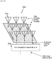
- FIGURE 5B illustrates a conceptual representation of a Tightly Coupled Antenna Array or Current Sheet Array with access to the antenna array virtual ports, according to embodiments of the present disclosure.
- the embodiment of the antenna array configuration 500b shown in FIGURE 5B is for illustration only. Other embodiments could be used without departing from the scope of the present disclosure.
- Each antenna element has a feeding port, which by means of a virtualization network 502b is mapped to a virtual port, at which an excitation can be applied.
- Port virtualization network aims to reduce the number of antenna array physical ports, M, to a smaller number of antenna array virtual ports, N ⁇ M.
- antenna array port can refer either to an antenna array physical port, or an antenna array virtual port.
- CSA antennas have the important advantages listed above, a significant drawback is that CSA antennas appear not to support MIMO communications.
- MIMO systems require no or low correlation among the antenna elements in a MIMO array.
- practical CSA arrays utilize tight electrical coupling among antenna elements to achieve low profiles and wide bandwidths. This tight coupling induces strong correlation among the antenna elements that cause strong correlation among any previously independent signals carried by the antenna elements of a CSA.
- the non-diagonal terms in the correlation matrix in Equation 2 would be large and the upper bound on the system capacity, C, would be low.
- Mutual coupling between antenna array elements is represented by the off-diagonal elements of matrices S RR and S TT .
- S RR and S TT would be diagonal and therefore full rank, thus preserving the rank of the channel matrix H.
- S RR and S TT would be full matrices and therefore very likely not full rank matrices or full rank matrices but with several small eigenvalues, thereby reducing the rank or efficiency of the overall communication link, thus reducing capacity.
- CSA antennas would appear to be wholly unsuitable for MIMO applications.
- the apparent failure of CSA antennas to support MIMO communications is the critical problem addressed by embodiments of the present disclosure.
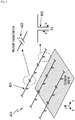
- FIGURE 6 illustrates an implementation of a linear Tightly Coupled Dipole Array over a ground plane according to embodiments of the present disclosure.
- the embodiment of the linear tightly coupled dipole Array 600 shown in FIGURE 6 is for illustration only. Other embodiments could be used without departing from the scope of the present disclosure.
- Mutual coupling is controlled via mutual capacitance, C, between adjacent dipoles by controlling the length of the overlapping sections of their arms.
- the transmitter or receiver array is a linear tightly coupled dipole array 600 placed over a ground plane, as shown in FIGURE 6 .
- the dipole elements are printed on printed circuit boards (PCB), which are arranged in rows placed perpendicularly to ground plane. Mutual coupling between dipole elements is controlled by overlapping sections of the dipole element arms 601.
- FIGURE 7 illustrates an implementation of a circular Tightly Coupled Dipole Array over a ground plane according to embodiments of the present disclosure.
- Mutual coupling is controlled via mutual capacitance, C, between adjacent dipoles by controlling the length of the overlapping sections of their arms.
- the transmitter or receiver array is a circular dipole array 700, as shown in FIGURE 7 .
- the dipole elements are printed on a printed circuit board (PCB), which are arranged in a plane parallel to the ground plane.
- PCB printed circuit board
- Mutual coupling between dipole elements is controlled by overlapping sections of dipole element arms, 701.
- FIGURE 8 illustrates an implementation of a circular Tightly Coupled Dipole Array over a ground plane according to embodiments of the present disclosure.
- the embodiment of the circular tightly coupled dipole array 800 shown in FIGURE 8 is for illustration only. Other embodiments could be used without departing from the scope of the present disclosure.
- Multiple concentric circular arrays can be used to achieve broadband or multi-band characteristics.
- Mutual coupling is controlled via mutual capacitance, C, between adjacent dipoles by controlling the length of the overlapping sections of their arms.
- the transmitter or receiver array is configured as an array of concentric circular dipole arrays 800, as shown in FIGURE 8 .
- the concentric circular arrays, 801, 802, 803, 804 can be placed at planes that have different distances from the ground plane, therefore allowing for multi-band or wideband operation.
- the dipole elements are printed on a printed circuit board (PCB), which are arranged in a plane parallel to the ground plane. Mutual coupling between dipole elements is controlled by overlapping sections of dipole element arms 701.
- PCB printed circuit board
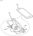
- FIGURE 9 illustrates a user equipment, such as a mobile phone, with three antennas placed along the edges of the metallic or plastic phone chassis according to embodiments of the present disclosure.
- the embodiment of the user equipment shown in FIGURE 9 is for illustration only. Other embodiments could be used without departing from the scope of the present disclosure.
- the mutual coupling between the antennas and the phone chassis can be controlled in the design process so as to establish certain Characteristic Modes, with specific resonant frequencies and orthogonal radiation patterns.
- the transmitter or receiver antenna array is a configuration of tightly coupled antenna elements that are not placed in a linear fashion, neither on a plane parallel to a ground plane.
- the UE can be configured as, for example, a mobile handset, such as a mobile phone 900, as shown in FIGURE 9 .
- tightly coupled antenna elements Antenna 1 901, Antenna 2 902, and Antenna 3 903 are disposed on or close to the mobile phone 900 chassis or casing of the mobile phone 900.
- Antenna 1 901, Antenna 2 902 and Antenna 3 903 can experience strong mutual coupling, unless special decoupling networks are used, or special placement on the phone chassis is exercised. This mutual coupling can be used advantageously according to other embodiments of the present disclosure, for enhanced MIMO operation.
- Antenna 1 901, Antenna 2 902 and Antenna 3 903 also strongly couple or induce currents to the phone chassis or casing.
- the mobile phone 900 casing can be metallic or plastic, or generally, of a material having a certain conductivity, permittivity and permeability.
- FIGURE 10 illustrates a Tightly Coupled Antenna Array or a Current Sheet Array on an integrated circuit (IC) die of a chip (for example CMOS or GaAS) according to embodiments of the present disclosure.
- IC integrated circuit
- FIGURE 10 illustrates a Tightly Coupled Antenna Array or a Current Sheet Array on an integrated circuit (IC) die of a chip (for example CMOS or GaAS) according to embodiments of the present disclosure.
- IC integrated circuit
- FIGURE 10 illustrates a Tightly Coupled Antenna Array or a Current Sheet Array on an integrated circuit (IC) die of a chip (for example CMOS or GaAS) according to embodiments of the present disclosure.
- the embodiment of the integrated circuit (IC) transceiver chip 1000 shown in FIGURE 10 is for illustration only. Other embodiments could be used without departing from the scope of the present disclosure.
- the transmitter or receiver antenna array is a configuration of tightly coupled antenna elements that are placed on the top surface of the die of an integrated circuit (IC) transceiver chip 1000, as shown, in FIGURE 10 .
- the antenna array can be formed by elements much smaller than the wavelength of operation or with antenna element spacing much smaller than the wavelength of operation, thereby with increased mutual coupling.
- Embodiments of the present disclosure are particularly useful in performing MIMO in this setting.
- FIGURE 11 illustrates an FD-MIMO telecommunications system including a user equipment, such as a mobile phone, and a base station according to embodiments of the present disclosure.
- the embodiment of the FD-MIMO telecommunications system 1100 shown in FIGURE 11 is for illustration only. Other embodiments could be used without departing from the scope of the present disclosure.
- the transceiver chip of FIGURE 10 is disposed in a mobile handset, such as a mobile phone, and be used in a MIMO system for communication with a base station as shown in FIGURE 11 .
- the IC transceiver might also include the RF transmit/receive chain, and the base-band unit (signal encoder/decoder) as shown in FIGURE 11 .
- FIGURE 12 illustrates current distributions of various Characteristic Modes on linear dipole arrays and their associated radiation patterns according to embodiments of the present disclosure.
- the embodiments of the current distributions shown in FIGURE 12 are for illustration only. Other embodiments could be used without departing from the scope of the present disclosure.
- the shaded region (light and dark color) on the array plane represents changes in the intensity of the modal current across the antenna array aperture.
- Characteristic Mode 1 1201 is associated with a broadside radiation pattern with wide beamwidth.
- Mode 2 1202 is associated with a tilted radiation pattern, pointing to a substantially different direction than Mode 1.
- Mode 3 1203 can be associated with a pattern exhibiting multiple main lobes, and Mode 4 1204 might be associated with a radiation pattern having a narrow and wide beamwidth in two orthogonal planes.
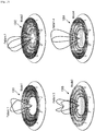
- FIGURE 13 illustrates Characteristic Mode current distributions on an array of concentric circular dipole arrays, such as the one shown in FIGURE 8 , according to embodiments of the present disclosure.
- the embodiments of the current distributions shown in FIGURE 13 are for illustration only. Other embodiments could be used without departing from the scope of the present disclosure.
- the shaded region (light and dark color) on the array plane represents changes in the intensity of the modal current across the antenna array aperture.
- Characteristic Mode 1 1301, Mode 2 1302, Mode 3 1303 and Mode 4 1304 can be associated with a variety of current distributions on the antenna array aperture, each having different intensities across the array aperture, designated by the darker and lighter color shades.
- the different modes might be associated with different radiation patterns, which are orthogonal in the far-field, and can therefore be used for MIMO.
- Mode 1 1301 is associated with a broadside radiation pattern with wide beamwidth.
- Mode 2 1302 is associated with a tilted radiation pattern, pointing to a substantially different direction than Mode 1.
- Mode 3 1303 can be associated with a pattern exhibiting multiple main lobes
- Mode 4 1304 can be associated with a radiation pattern having a narrow and wide beamwidth in two orthogonal planes.
- the transmitter or receiver antenna array is configured as tightly coupled antenna elements that are not placed in a linear or circular fashion, neither on a plane parallel to a ground plane.
- a configuration can be a mobile handset, such as a mobile phone, 900, as shown in FIGURE 9 .
- tightly coupled antenna elements Antenna 1 901, Antenna 2 902, and Antenna 3 903 are disposed on, or close to, the mobile phone 900 chassis or casing of the mobile phone 900. Strong coupling might also occur between the antenna elements and the phone chassis, causing strong currents to be excited on the latter.
- FIGURE 14 illustrates exemplary Characteristic Mode radiation patterns associated with an antenna array placed on a metallic or plastic phone chassis according to embodiments of the present disclosure.
- the embodiments of the radiation patterns shown in FIGURE 14 are for illustration only. Other embodiments could be used without departing from the scope of the present disclosure.
- By exciting the antenna elements with certain amplitude/phase weights, or excitation coefficients, as shown in the table different radiation patterns corresponding to Characteristic Modes can be obtained.
- the phone or device chassis can be designed to assist with or provide extra characteristic modes by coupling to the antennas.
- Antenna 1, Antenna 2 and Antenna 3 can be excited with different excitation coefficients or excitation weights, respectively w1, w2 and w3.
- the different weight combinations will result in exciting different characteristic modes.
- various radiation patterns can be obtained such as a first radiation pattern for a first characteristic mode 1401, a second radiation pattern for a second characteristic mode 1402, and a third radiation pattern for a third characteristic mode 1403.
- Table 1 is an example of the antenna array excitation weights used to excite characteristic mode 1, mode 2 and mode 3, associated respectively with radiation patterns 1401, 1402, and 1403. TABLE 1 Ant # Excitation Coefficient Mode 1 Mode 2 Mode 3 Ant 1 w1 0.7 1 0.2 Ant 2 w2 1 0.7 0.5 Ant 3 w3 0.4 0.8 1
- FIGURE 15 illustrates Characteristic Mode currents and wave-fronts associated with a Tightly Coupled Array antenna or Current Sheet Antenna on a chip according to embodiments of the present disclosure.
- the embodiment of the currents and wave-fronts shown in FIGURE 15 is for illustration only. Other embodiments could be used without departing from the scope of the present disclosure.
- the 3-D shaded region (light and dark color) represents changes in the field intensity of the various modes across the antenna array aperture.
- FIGURE 15 exemplary characteristic mode current or electric field distributions on or above the surface of a tightly coupled patch antenna array or current sheet array, placed on a the die of a transceiver integrated circuit (IC) 1500, are illustrated.
- the tightly coupled patch elements allow for excitation of various Characteristic Modes 1501, 1502 and 1503, which can carry different signals and radiate them in different, orthogonal radiation patterns, according to embodiments of the present disclosure.
- FIGURE 16 illustrates a diagram of a system implementation for estimating the Characteristic Mode excitation coefficients of an antenna array by measuring the antenna array port scattering matrix (S-matrix) and converting the S-matrix to an equivalent impedance matrix (Z-matrix) according to embodiments of the present disclosure.
- the embodiment of the system 1600 shown in FIGURE 16 is for illustration only. Other embodiments could be used without departing from the scope of the present disclosure.
- the associated table provides an exemplary measurement sequence of the S-matrix for a two-element antenna array.
- the antenna array port scattering matrix, S is measured on-the-fly.
- An example of an implementation of a circuit to perform the S-matrix measurement is the system 1600 shown in FIGURE 16 for an antenna array comprised of two elements only.
- the system 1600 is to be used for illustration purposes and should not be construed to limit the scope of this disclosure.
- the system 1600 can be easily scaled to include multiple antennas.
- the system 1600 is configured to: use a combination of two-state switches 1601, namely TR switch #1 1601a, switch #2 1601b and switch #1 1602a and switch #2 1602b along with directional couplers 1603 and circulators 1604, enable a measurement of the antenna array port S-matrix, namely S 11 , S 12 , S 21 , S 22 . That is, system 1600 is configured to perform a measurement of the antenna array port S-matrix. Table 2 shows the measurement sequence to obtain S 11 , S 12 , S 21 , and S 22 .
- the measured S-matrix phase reference obtained by the implementation of system 1600 can be placed at the antenna array ports.
- the S-matrix is obtained at the antenna physical ports or at the antenna array virtual ports.
- the antenna array port scattering matrix S (S-matrix) or the antenna array port impedance matrix Z (Z- matrix)
- S-matrix or the antenna array port impedance matrix Z (Z- matrix)
- Z- matrix can be directly acquired by numerical simulation of the antenna array by using a computational electromagnetics software, and stored in a memory for further post-processing.
- the antenna array port impedance matrix Z is obtained and stored in a memory, either by means of measurement or a-priori numerical simulation, according to embodiments of the present disclosure, calculation of the appropriate orthogonal modes to be used for MIMO can take place.
- the antenna array port Characteristic Modes are extracted from the antenna array port impedance matrix Z and used for MIMO.
- the antenna array port Inagaki modes are extracted from the antenna array port impedance matrix Z and used for MIMO.
- the antenna array port eigenmodes are extracted from the antenna array port scattering matrix S and used for MIMO.
- Equations. 7, 8, and 9 are evaluated at a first frequency.
- Equations 7, 8, and 9 are evaluated at a first and second frequency.
- Equations. 7, 8, and 9 are evaluated over a wideband frequency range.
- the eigenmodes and eigenvalues can be stored in a memory for further post processing.
- a modal intensity factor or modal significance parameter, ⁇ is calculated and stored in a memory.
- the purpose of ⁇ is to scale the modal eigenvalues ⁇ , ranging in magnitude from (0, ⁇ ), in the range from [0,1].
- ⁇ is the eigenvalue of each mode I.
- Equation 10 is to be used as an example of scaling the modal eigenvalues ⁇ , and not for limiting the scope of the present disclosure. It is understood that one could use an alternative scaling or normalization of the modal eigenvalues ⁇ .
- the modal significance parameter ⁇ is used to prioritize or order the eigenmodes.
- the array port excitation coefficients or array port weights can be calculated.
- either the Characteristic Modes or the Inagaki modes are chosen as the desired set of orthogonal array port eigenmodes.
- the array port excitation coefficients can be calculated.
- the process outlined in embodiments of the present disclosure, of calculating the antenna array port excitation coefficients, is only used for exemplary purposes and not for limiting the scope of the present disclosure. It is understood that one could use an alternative mathematical calculation to extract the antenna array port excitation coefficients.
- Z is the antenna array port impedance matrix
- I is the Characteristic or Inagaki eigenmode, respectively given by Equation 7 and Equation 8, that is desired to be excited.
- Voltage V is stored in a memory for further post processing.
- an optimum impedance matching condition is realized at the antenna array ports by means of an impedance matching circuit 1903, such as shown in FIGURE 19 .
- the impedance matching circuit 1903 converts the system impedance used on the right side of the impedance matching circuit 1903, typically set to 50 ⁇ , to the desired impedance at the antenna array port on the left side of the matching circuit.
- the Characteristic or Inagaki eigenmode, I is a linear combination of orthogonal eigenmodes.
- the array port excitation coefficients (amplitude and phase) and impedance matching values are applied with certain amplitude and phase tolerance, such as 10% of the calculated value, without much loss of antenna radiation efficiency.
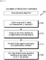
- FIGURE 17 illustrates an exemplary array excitation process according to embodiments of the present disclosure.
- the embodiments of the algorithm 1700 shown in FIGURE 17 is for illustration only. While the flow chart depicts a series of sequential steps, unless explicitly stated, no inference should be drawn from that sequence regarding specific order of performance, performance of steps or portions thereof serially rather than concurrently or in an overlapping manner, or performance of the steps depicted exclusively without the occurrence of intervening or intermediate steps.
- the process depicted in the example depicted is implemented by a transmitter chain in, for example, a mobile station.
- the algorithm 1700 for calculating and applying the desired antenna array port excitation coefficients associated with a certain set of orthogonal modes such as the array port Characteristic Modes or the Inagaki modes is outlined in FIGURE 17 . It is understood that this algorithm 1700 is an example of calculating and applying the desired antenna array port excitation coefficients associated with a certain set of orthogonal modes and should not be used to limit the scope of this invention disclosure.
- the algorithm 1700 shows the four basic steps for determining antenna array port excitation coefficients.
- array port S-matrix is obtained via measurement (or via simulation which is not part of the present invention) by estimating the antenna array port mutual coupling scattering matrix S (at the physical or virtual ports).
- a desired set of eigenmodes and eigenvalues are computed and stored in a memory.
- a maximum modal significance parameter ⁇ a maximum radiation efficiency, a maximum SINR at the user, a minimum interference at the user, a maximum system capacity, a maximum radiation efficiency, or a combination of the above.
- an antenna array excitation table with the antenna excitation coefficients a ij , (coefficient of antenna port i to excite a Characteristic Mode j), and associated port system impedances Z 0,ij is calculated and the calculated antenna weights and characteristic impedances at RF or Baseband (BB) domains are applied.
- BB Baseband
- the array port excitation coefficients and matching impedances can be applied to the antenna array ports(physical or virtual ports).
- An exemplary diagram showing an application of such a set of antenna array port excitation coefficients is shown in FIGURE 18 .
- FIGURE 18A illustrates an exemplary implementation of a feed network for transmitting or receiving two signals S1 and S2 associated with two Characteristic Modes, by applying the appropriate Characteristic Mode excitation coefficients (amplitude a i j , and phase ⁇ i j ) to an antenna array, via use of combiner/splitter network according to embodiments of the present disclosure.
- the embodiment of the feed network 1800 shown in FIGURE 18A is for illustration only. Other embodiments could be used without departing from the scope of the present disclosure.
- signals S1 1803a and S2 1803b are each assigned to an orthogonal mode 1 and 2, such as those described by embodiments of the present disclosure.
- a network of signal combiners/splitters 1804 distributes those signals to M antenna ports 1801.
- Signals S1 and S2 are assigned to an orthogonal mode, such as those described by embodiments of the present disclosure, by being multiplied with the corresponding array port excitation coefficient (amplitude and phase) or weight 1805.
- the weighted signals are then summed or combined via a network of signal summation blocks 1802 prior to transmission by the antenna terminals.
- FIGURE 18B A simplified representation of this process is illustrated in the example shown in FIGURE 18B .
- FIGURE 18B illustrates an implementation of a Current Sheet Antenna or Tightly Coupled Array for transmitting or receiving two signals S1 and S2 associated with two characteristic modes, by applying the appropriate Characteristic Mode excitation coefficients (amplitude a i j , and phase ⁇ i j ) to an antenna array, via use of a power combiner/splitter network according to embodiments of the present disclosure.
- the embodiment of the CSA shown in FIGURE 18B is for illustration only. Other embodiments could be used without departing from the scope of the present disclosure.
- the desired antenna array port excitation coefficients associated with a certain set of orthogonal modes can be applied to the antenna array ports in the RF or Base band (BB) domains.
- BB Base band
- FIGURE 19 illustrates an implementation for applying Orthogonal Mode excitation coefficients (amplitude a i j , and phase ⁇ i j ) and antenna array port system impedance Z 0,ij , at a hardware level in the RF domain according to embodiments of the present disclosure.
- the embodiment of the Characteristic Mode Excitation system 1900 shown in FIGURE 19 is for illustration only. Other embodiments could be used without departing from the scope of the present disclosure.
- the antenna array excitation coefficients are applied to the antenna array ports in the RF domain by the Orthogonal Mode Excitation system 1900.
- Characteristic Mode Excitation system 1900 is provided for exemplary purposes and other embodiments could be used without departing from the scope of the present disclosure.
- Characteristic Mode Excitation system 1900 can include an alternative hardware architecture to implement the desired antenna array port excitation coefficients.
- the Characteristic Mode Excitation system 1900 includes basic implementation blocks that perform amplitude control 1901, related to the amplitude of the antenna array port excitation coefficient, phase control 1902, related to the phase of the antenna array port excitation coefficient, and impedance matching control 1903, related to the desired matching impedance for each antenna array element.
- the desired orthogonal modes to be used for MIMO are stored in a lookup table 1904.
- a signal to be transmitted via a desired orthogonal mode as described in certain embodiments of the present disclosure, is generated at baseband and up-converted to the RF domain, via a frequency mixer and appropriate filtering.
- the desired mode excitation coefficient (amplitude and phase) is applied at each RF chain, connected to each antenna port, via an amplitude control block 1901, such as a variable gain attenuator and a phase control block, such as a phase shifter 1902.
- the signal then is amplified and, after the appropriate impedance matching control block 1903, is propagated into space by the radiation pattern of the desired orthogonal mode.
- FIGURE 20 illustrates an implementation for applying enforcing Orthogonal Mode Excitation coefficients (amplitude a i j , and phase ⁇ i j ), such as for example Characteristic Mode Excitation coefficients, at software level in the baseband domain, and antenna array port system impedance Z 0,ij , at a hardware level in the RF domain according to embodiments of the present disclosure.
- the embodiment of the Characteristic Mode Excitation system 2000 shown in FIGURE 20 is for illustration only. Other embodiments could be used without departing from the scope of the present disclosure.
- the antenna array excitation coefficients are applied to the antenna array ports in the Base band (BB) domain by the Characteristic Mode Excitation system 2000.
- Characteristic Mode Excitation system 2000 is provided for exemplary purposes and other embodiments could be used without departing from the scope of the present disclosure.
- Characteristic Mode Excitation system 2000 can include an alternative architecture to implement the desired antenna array port excitation coefficients.
- the desired orthogonal modes to be used for MIMO are stored in a lookup table 2002.
- a signal to be transmitted via a desired orthogonal mode as described in certain embodiments of the present disclosure, is generated at baseband and assigned the specified weight related to the array port excitation coefficient for the desired orthogonal mode.
- the signal is up-converted to the RF domain, via a frequency mixer and appropriate filtering.
- the signal is then amplified and, after the appropriate impedance matching control block 2001, is propagated into space by the radiation pattern of the desired orthogonal mode.
- embodiments of the present disclosure can be implemented with any number of antenna types and antenna array configurations. Additionally, elements from each of the embodiments can be combined with one or more other embodiments of the present disclosure.
- the antenna arrays are described as tightly coupled arrays or current sheet antennas (CSA), however any type of antenna array in which the antenna elements have strong mutual coupling could be used without departing from the scope of the disclosure. Therefore, embodiments of the present disclosure can be implemented at nearly any carrier frequency (1 MHz to 300 GHz) but restricted to the operating frequency range of intended specified antenna array used with the embodiment. The number of characteristic modes that the antenna array will support will depend upon the electrical size of the antenna array and number of array elements.
- a MIMO antenna array according to certain embodiments of the present disclosure will be smaller than a MIMO array of a conventional design.
- the antenna arrays for certain embodiments can be constructed in planar, circular or irregular array grid, and by using nearly any fabrication technology: printed circuit board (PCB), stamped or formed metal, ceramic substrates with printed metal conductors (e.g., LTCC), integrated antennas in microelectronic devices (i.e., integrated circuits), antennas in IC packaging, and the like.
- PCB printed circuit board
- LTCC printed metal conductors
- integrated antennas in microelectronic devices i.e., integrated circuits
- antennas in IC packaging and the like.
- excitation of the characteristic modes in the antenna array requires weighting of the signals at the antenna ports with complex coefficients.
- the complex weightings can be applied to the signals either in the RF domain using RF amplifiers or variable gain attenuators and RF phase shifters.
- the complex weightings can be applied in the base-band domain through digital signal processing techniques prior to the up- or downconversion of the signals between RF and base-band domains.
- the exact implementation will depend upon the demands and restrictions of a particular application.
- the antenna element types that can be used with the certain embodiments include, but are not limited to: linear antennas, dipoles, monopoles, patch antennas, slot antennas, inverted F, planar inverted F, spiral antennas, log periodic, Yagi-Uda, substrate integrated waveguide antennas, dielectric resonator antennas, and variations on the aforementioned types.
- FIGURE 21 illustrates an example wireless network 2100 according to this disclosure.
- the embodiment of the wireless network 2100 shown in FIGURE 21 is for illustration only. Other embodiments of the wireless network 2100 could be used without departing from the scope of this disclosure.
- the wireless network 2100 includes or is configured as the FD-MIMO system 100.
- the wireless network 2100 includes an eNodeB (eNB) 2101, an eNB 2102, and an eNB 2103.
- the eNB 2101 communicates with the eNB 2102 and the eNB 2103.
- the eNB 2101 also communicates with at least one Internet Protocol (IP) network 2130, such as the Internet, a proprietary IP network, or other data network.
- IP Internet Protocol
- eNodeB eNodeB
- eNB base station
- access point eNodeB
- eNodeB and eNB are used in this patent document to refer to network infrastructure components that provide wireless access to remote terminals.
- UE user equipment
- mobile station such as a mobile telephone or smartphone
- remote terminal such as a desktop computer or vending machine
- the eNB 2102 provides wireless broadband access to the network 2130 for a first plurality of user equipments (UEs) within a coverage area 2120 of the eNB 2102.
- the first plurality of UEs includes a UE 2111, which may be located in a small business (SB); a UE 2112, which may be located in an enterprise (E); a UE 2113, which may be located in a WiFi hotspot (HS); a UE 2114, which may be located in a first residence (R); a UE 2115, which may be located in a second residence (R); and a UE 2116, which may be a mobile device (M) like a cell phone, a wireless laptop, a wireless PDA, or the like.
- M mobile device
- the eNB 2103 provides wireless broadband access to the network 2130 for a second plurality of UEs within a coverage area 2125 of the eNB 2103.
- the second plurality of UEs includes the UE 2115 and the UE 2116.
- one or more of the eNBs 2101-2103 may communicate with each other and with the UEs 2111-2116 using 5G, LTE, LTE-A, WiMAX, or other advanced wireless communication techniques.
- Dotted lines show the approximate extents of the coverage areas 2120 and 2125, which are shown as approximately circular for the purposes of illustration and explanation only. It should be clearly understood that the coverage areas associated with eNBs, such as the coverage areas 2120 and 2125, may have other shapes, including irregular shapes, depending upon the configuration of the eNBs and variations in the radio environment associated with natural and man-made obstructions.
- various components of the network 2100 include tightly coupled antenna arrays or support a miniaturization of MIMO systems via tightly coupled antenna arrays.
- FIGURE 21 illustrates one example of a wireless network 2100
- the wireless network 2100 could include any number of eNBs and any number of UEs in any suitable arrangement.
- the eNB 2101 could communicate directly with any number of UEs and provide those UEs with wireless broadband access to the network 2130.
- each eNB 2102-2103 could communicate directly with the network 2130 and provide UEs with direct wireless broadband access to the network 2130.
- the eNB 2101, 2102, and/or 2103 could provide access to other or additional external networks, such as external telephone networks or other types of data networks.
- FIGURE 22 illustrates an example UE 2114 according to this disclosure.
- the embodiment of the UE 2114 shown in FIGURE 22 is for illustration only, and the other UEs in FIGURE 21 could have the same or similar configuration.
- UEs come in a wide variety of configurations, and FIGURE 22 does not limit the scope of this disclosure to any particular implementation of a UE.
- the UE 2114 includes an antenna 2205, a radio frequency (RF) transceiver 2210, transmit (TX) processing circuitry 2215, a microphone 2220, and receive (RX) processing circuitry 2225.
- the UE 2114 also includes a speaker 2230, a main processor 2240, an input/output (I/O) interface (IF) 2245, a keypad 2250, a display 2255, and a memory 2260.
- the memory 2260 includes a basic operating system (OS) program 2261 and one or more applications 2262.
- OS basic operating system
- the RF transceiver 2210 receives, from the antenna 2205, an incoming RF signal transmitted by an eNB or another UE.
- the RF transceiver 2210 down-converts the incoming RF signal to generate an intermediate frequency (IF) or baseband signal.
- the IF or baseband signal is sent to the RX processing circuitry 2225, which generates a processed baseband signal by filtering, decoding, and/or digitizing the baseband or IF signal.
- the RX processing circuitry 2225 transmits the processed baseband signal to the speaker 2230 (such as for voice data) or to the main processor 2240 for further processing (such as for web browsing data).
- the TX processing circuitry 2215 receives analog or digital voice data from the microphone 2220 or other outgoing baseband data (such as web data, e-mail, or interactive video game data) from the main processor 2240.
- the TX processing circuitry 2215 encodes, multiplexes, and/or digitizes the outgoing baseband data to generate a processed baseband or IF signal.
- the RF transceiver 2210 receives the outgoing processed baseband or IF signal from the TX processing circuitry 2215 and up-converts the baseband or IF signal to an RF signal that is transmitted via the antenna 2205.
- the main processor 2240 can include one or more processors or other processing devices and can execute the basic OS program 2261 stored in the memory 2260 in order to control the overall operation of the UE 2114.
- the main processor 2240 could control the reception of forward channel signals and the transmission of reverse channel signals by the RF transceiver 2210, the RX processing circuitry 2225, and the TX processing circuitry 2215 in accordance with well-known principles.
- the main processor 2240 includes at least one microprocessor or microcontroller.
- the main processor 2240 is also capable of executing other processes and programs resident in the memory 2260 such as operations in support of communication with aggregation of FDD cells and TDD cells.
- the main processor 2240 can move data into or out of the memory 2260 as required by an executing process.
- the main processor 2240 is configured to execute the applications 2262 based on the OS program 2261 or in response to signals received from eNBs, other UEs, or an operator.
- the main processor 2240 is also coupled to the I/O interface 2245, which provides the UE 2114 with the ability to connect to other devices such as laptop computers and handheld computers.
- the I/O interface 2245 is the communication path between these accessories and the main processor 2240.
- the main processor 2240 is also coupled to the keypad 2250 and the display unit 2255.
- the operator of the UE 2114 can use the keypad 2250 to enter data into the UE 2114.
- the display 2255 may be a liquid crystal display or other display capable of rendering text and/or at least limited graphics, such as from web sites.
- the display 2255 could also represent a touchscreen.
- the memory 2260 is coupled to the main processor 2240.
- Part of the memory 2260 could include a random access memory (RAM), and another part of the memory 2260 could include a Flash memory or other read-only memory (ROM).
- RAM random access memory
- ROM read-only memory
- the transmit and receive paths of the UE 2114 include tightly coupled antenna arrays or support a miniaturization of MIMO systems via tightly coupled antenna arrays.
- FIGURE 22 illustrates one example of UE 2114
- various changes may be made to FIGURE 22 .
- various components in FIGURE 22 could be combined, further subdivided, or omitted and additional components could be added according to particular needs.
- the main processor 2240 could be divided into multiple processors, such as one or more central processing units (CPUs) and one or more graphics processing units (GPUs).
- FIGURE 22 illustrates the UE 2114 configured as a mobile telephone or smartphone, UEs could be configured to operate as other types of mobile or stationary devices.
- various components in FIGURE 22 could be replicated, such as when different RF components are used to communicate with the eNBs 2101-2103 and with other UEs.
- FIGURE 23 illustrates an example eNB 2102 according to this disclosure.
- the embodiment of the eNB 2102 shown in FIGURE 23 is for illustration only, and other eNBs of FIGURE 21 could have the same or similar configuration.
- eNBs come in a wide variety of configurations, and FIGURE 23 does not limit the scope of this disclosure to any particular implementation of an eNB.
- the eNB 2102 includes multiple antennas 2305a-2305n, multiple RF transceivers 2310a-2310n, transmit (TX) processing circuitry 2315, and receive (RX) processing circuitry 2320.
- the eNB 2102 also includes a controller/processor 2325, a memory 2330, and a backhaul or network interface 2335.
- the RF transceivers 2310a-2310n receive, from the antennas 2305a-2305n, incoming RF signals, such as signals transmitted by UEs or other eNBs.
- the RF transceivers 2310a-2310n down-convert the incoming RF signals to generate IF or baseband signals.
- the IF or baseband signals are sent to the RX processing circuitry 2320, which generates processed baseband signals by filtering, decoding, and/or digitizing the baseband or IF signals.
- the RX processing circuitry 2320 transmits the processed baseband signals to the controller/ processor 2325 for further processing.
- the TX processing circuitry 2315 receives analog or digital data (such as voice data, web data, e-mail, or interactive video game data) from the controller/processor 2325.
- the TX processing circuitry 2315 encodes, multiplexes, and/or digitizes the outgoing baseband data to generate processed baseband or IF signals.
- the RF transceivers 2310a-2310n receive the outgoing processed baseband or IF signals from the TX processing circuitry 2315 and up-converts the baseband or IF signals to RF signals that are transmitted via the antennas 2305a-2305n.
- the controller/processor 2325 can include one or more processors or other processing devices that control the overall operation of the eNB 2102.
- the controller/processor 2325 could control the reception of forward channel signals and the transmission of reverse channel signals by the RF transceivers 2310a-2310n, the RX processing circuitry 2320, and the TX processing circuitry 2315 in accordance with well-known principles.
- the controller/processor 2325 could support additional functions as well, such as more advanced wireless communication functions.
- the controller/processor 2325 could support beam forming or directional routing operations in which outgoing signals from multiple antennas 2305a-2305n are weighted differently to effectively steer the outgoing signals in a desired direction. Any of a wide variety of other functions could be supported in the eNB 2102 by the controller/processor 2325.
- the controller/ processor 2325 includes at least one microprocessor or microcontroller.
- the controller/processor 2325 is also capable of executing programs and other processes resident in the memory 2330, such as a basic OS.
- the controller/processor 2325 can move data into or out of the memory 2330 as required by an executing process.
- the controller/processor 2325 is also coupled to the backhaul or network interface 2335.
- the backhaul or network interface 2335 allows the eNB 2102 to communicate with other devices or systems over a backhaul connection or over a network.
- the interface 2335 could support communications over any suitable wired or wireless connection(s).
- the eNB 2102 is implemented as part of a cellular communication system (such as one supporting 5G, LTE, or LTE-A)
- the interface 2335 could allow the eNB 2102 to communicate with other eNBs over a wired or wireless backhaul connection.
- the interface 2335 could allow the eNB 2102 to communicate over a wired or wireless local area network or over a wired or wireless connection to a larger network (such as the Internet).
- the interface 2335 includes any suitable structure supporting communications over a wired or wireless connection, such as an Ethernet or RF transceiver.
- the memory 2330 is coupled to the controller/processor 2325. Part of the memory 2330 could include a RAM, and another part of the memory 2330 could include a Flash memory or other ROM.
- the transmit and receive paths of the eNB 2102 include tightly coupled antenna arrays or support a miniaturization of MIMO systems via tightly coupled antenna arrays.
- FIGURE 23 illustrates one example of an eNB 2102
- the eNB 2102 could include any number of each component shown in FIGURE 23 .
- an access point could include a number of interfaces 2335, and the controller/processor 2325 could support routing functions to route data between different network addresses.
- the eNB 2102 while shown as including a single instance of TX processing circuitry 2315 and a single instance of RX processing circuitry 2320, the eNB 2102 could include multiple instances of each (such as one per RF transceiver).
- FIGURES 1 through 16 and 18-23 are for illustration only. Each component could have any suitable size, shape, and dimensions, and multiple components could have any suitable arrangement and layout. Also, various components in FIGURES 1 through 16 and 18-23 could be combined, further subdivided, or omitted and additional components could be added according to particular needs. Further, each component in a device or system could be implemented using any suitable structure(s) for performing the described function(s). In addition, while FIGURE 17 illustrates various series of steps, various steps in FIGURE 17 could overlap, occur in parallel, occur multiple times, or occur in a different order.
Landscapes
- Engineering & Computer Science (AREA)
- Computer Networks & Wireless Communication (AREA)
- Signal Processing (AREA)
- Variable-Direction Aerials And Aerial Arrays (AREA)
- Radio Transmission System (AREA)
Description
- The present disclosure relates to Full Dimension Multiple Input Multiple Output (FD-MIMO) systems with multiple active antennas at transmitter (base station), a receiver (user station), or both.
- Recently, a new Multiple-Input-Multiple-Output (MIMO) system, called the Full-dimensional MIMO (FD-MIMO), has shown great potential to improve the spectral efficiency of the current Long Term Evolution (LTE) networks. The FD-MIMO system applies a large number of active antenna elements arranged in a two-dimensional manner at the Base-Station (BS). The antenna array is capable of beamforming in both azimuth and elevation directions, and capable of providing sufficient degrees of freedom to support high order MultiUser MIMO (MU-MIMO).
- TZUNG-I LEE ET AL: "Mode-Based Information Channels in Closely Coupled Dipole Pairs", IEEE TRANS. ON ANTENNAS AND PROPAGATION, IEEE, vol. 56, no. 12, 1 December 2008, pages 3804-3811, discloses information channels supported by two orthogonal radiation modes in a pair of closely spaced dipole antennas..
- Ioannis Tzanidis ET AL: "Ultrawideband Low-Profile Arrays of Tightly Coupled. Antenna Elements: Excitation, Termination and Feeding Methods" 20 october 2011, discloses an excitation technique based on the characteristic modes (CM) of the mutual impedance matrix of the array.
- S.-L Zuo ET AL: "Eigenmode decoupling for MIMO loop-antenna based on 180 degrees coupler", Progress In Electromagnetics Research Letters, 1 June 2011, pages 11-20, discloses a low-cost, high isolation, printed loop-antenna system for multiple-input multiple-output (MIMO) applications in the 2.4 GHz WLAN band.
- Jonathan Ethier: "MIMO Antenna Design Using characteristic Mode Concepts", Masters Thesis, 6 june 2008 discloses how characteristic mode (CM) theory can be used to in the design of the antennas with the low envelope correlation coefficients preferred for MIMO antennas. JONATHAN ETHIER ET AL: "Through the looking glass: A characteristic mode view of electromagnetic modelling and design", ANTENNA TECHNOLOGY AND APPLIED ELECTROMAGNETICS & THE AMERICAN ELECTROMAGNETICS CONFERENCE (ANTEM-AMEREM), 2010 14TH INT. SYMP., IEEE, 5 July 2010, pages 1-4, discloses how electromagnetic structure can be analysed in terms of its so-called characteristic modes at any frequency
- In an embodiment, a method is provided. The method is configured to generate Multiple Input Multiple Output (MIMO) signals in a wireless propagation channel using antenna array port orthogonal modes. The method includes measuring an antenna array port scattering matrix S at a first frequency from an antenna array comprising tightly coupled antenna array elements. The method also includes determining, a set of antenna array port orthogonal modes, wherein the set of antenna array port orthogonal modes include an antenna array port characteristic mode based on antenna array port scattering matrix S at the first frequency. In addition, the method includes determining an ordering of the antenna array port orthogonal at the first frequency based on system performance criteria. The system performance criteria includes one or more of: a maximum modal significance parameter α, a maximum radiation efficiency, a maximum signal to interference noise ratio (SINR) at a user terminal, a minimum interference at the user terminal, and a maximum capacity of a system in which the apparatus is configured. The method also includes determining antenna array port excitation coefficients at the first frequency based on the ordering of the antenna array port characteristic modes at the first frequency. Further, the method includes applying the antenna array port excitation coefficients as antenna array port excitation weights, wherein the maximum modal significance parameter is determined based on a magnitude of a modal eigenvalue for each of the antenna array port characteristic modes, wherein the maximum modal significance parameter is in a range of [0, 1], and wherein the maximum modal significance parameter is given as:

- In an embodiment, an apparatus is provided. The apparatus includes processing circuitry configured to generate Multiple Input Multiple Output (MIMO) signals in a wireless propagation channel using antenna array port orthogonal modes. The apparatus also includes an antenna array that includes at least two tightly coupled antennas at a first frequency. The apparatus further includes a memory configured to store a plurality of instructions. The plurality of instructions are configured to cause the processing circuitry to: measure an antenna array port scattering matrix S at the first frequencys; determine a set of antenna array port orthogonal modes, wherein the set of antenna array port orthogonal modes include antenna array port characteristic modes based on antenna array port scattering matrix S at the first frequency; determine an ordering of the antenna array port orthogonal modes at the first frequency based on a system performance criteria, the system performance criteria comprising one or more of: a maximum modal significance parameter α, a maximum radiation efficiency, a maximum signal to interference noise ratio (SINR) at a user terminal, a minimum interference at the user terminal, and a maximum capacity of a system in which the apparatus is configured; determine antenna array port excitation coefficients at the first frequency based on the ordering of the antenna array port characteristic modes and the antenna array port characteristics modes at the first frequency; and apply the antenna array port excitation coefficients as antenna array port excitation weights, wherein the maximum modal significance parameter is determined based on a magnitude of a modal eigenvalue for each of the antenna array port characteristic modes, wherein the maximum modal significance parameter is in a range of [0, 1], and wherein the maximum modal significance parameter is given as:

- For a more complete understanding of the present disclosure and its advantages, reference is now made to the following description taken in conjunction with the accompanying drawings, in which like reference numerals represent like parts:
-
FIGURE 1 illustrates an FD-MIMO (Full Dimension MIMO) base station along with user equipment according to embodiments of the present disclosure; -
FIGURE 2 illustrates a propagation environment between a transmitter antenna array and a receiver antenna array according to embodiments of the present disclosure;. -
FIGURE 3 illustrates a conceptual representation of a Current Sheet Antenna or a Tightly Coupled Array placed above a ground plane according to embodiments of the present disclosure; -
FIGURE 4 illustrates a conceptual circuit representation of a Current Sheet Antenna or a Tightly Coupled Array of dipole antennas placed above a ground plane according to embodiments of the present disclosure; -
FIGURE 5A illustrates a conceptual representation of a Tightly Coupled Antenna Array or Current Sheet Array with access to the antenna array physical ports according to embodiments of the present disclosure; -
FIGURE 5B illustrates a conceptual representation of a Tightly Coupled Antenna Array or Current Sheet Array with access to the antenna array virtual ports, according to embodiments of the present disclosure; -
FIGURE 6 illustrates an implementation of a linear Tightly Coupled Dipole Array over a ground plane according to embodiments of the present disclosure; -
FIGURE 7 illustrates an implementation of a circular Tightly Coupled Dipole Array over a ground plane according to embodiments of the present disclosure; -
FIGURE 8 illustrates an implementation of a circular Tightly Coupled Dipole Array over a ground plane according to embodiments of the present disclosure; -
FIGURE 9 illustrates a user equipment with three antennas placed along the edges of the metallic or plastic phone chassis according to embodiments of the present disclosure; -
FIGURE 10 illustrates a Tightly Coupled Antenna Array or a Current Sheet Array on a die of an integrated circuit (IC) chip (for example CMOS or GaAS) according to embodiments of the present disclosure; -
FIGURE 11 illustrates an FD-MIMO telecommunications system including a user equipment and a base station according to embodiments of the present disclosure; -
FIGURE 12 illustrates exemplary current distributions of various Characteristic Modes on linear dipole arrays and their associated radiation patterns according to embodiments of the present disclosure; -
FIGURE 13 illustrates exemplary current distributions of various Characteristic Modes on circular dipole arrays and their associated radiation patterns according to embodiments of the present disclosure; -
FIGURE 14 illustrates exemplary Characteristic Mode radiation patterns associated with an antenna array placed on a metallic or plastic phone chassis according to embodiments of the present disclosure; -
FIGURE 15 illustrates exemplary Characteristic Mode currents and wave-fronts associated with a Tightly Coupled Array antenna or Current Sheet Antenna on a chip according to embodiments of the present disclosure; -
FIGURE 16 illustrates a diagram of a system implementation for estimating the Characteristic Mode excitation coefficients of an antenna array by measuring the antenna arrays scattering matrix (S-matrix) and converting it to an equivalent impedance matrix (Z-matrix) according to embodiments of the present disclosure; -
FIGURE 17 illustrates an array excitation process according to embodiments of the present disclosure; -
FIGURE 18A illustrates an implementation of a feed network for transmitting or receiving two signals S1 and S2 associated with two Characteristic Modes, by applying the appropriate Characteristic Mode excitation coefficients (amplitude ai j , and phase ϕi j ) to an antenna array, via use of combiner/splitter network according to embodiments of the present disclosure;. -
FIGURE 18B illustrates an implementation of a Current Sheet Antenna or Tightly Coupled Array for transmitting or receiving two signals S1 and S2 associated with two characteristic modes, by applying the appropriate Characteristic Mode excitation coefficients (amplitude ai j , and phase ϕi j ) to an antenna array, via use of a power combiner/splitter network according to embodiments of the present disclosure; -
FIGURE 19 illustrates an implementation for applying Characteristic Mode excitation coefficients (amplitude ai j , and phase ϕi j ) and antenna array port system impedance Z0,ij, at a hardware level in the RF domain according to embodiments of the present disclosure; -
FIGURE 20 illustrates an implementation for applying enforcing Characteristic Mode excitation coefficients (amplitude ai j , and phase ϕi j ) at software level in the baseband domain, and antenna array port system impedance Z0,ij , at a hardware level in the RF domain according to embodiments of the present disclosure; -
FIGURE 21 illustrates an example wireless communication network according to this disclosure; -
FIGURE 22 illustrates an example user equipment (UE) according to this disclosure; and -
FIGURE 23 illustrates an example eNodeB (eNB) according to this disclosure. -
FIGURES 1 through 23 , discussed below, and the various embodiments used to describe the principles of the present disclosure in this patent document are by way of illustration only and should not be construed in any way to limit the scope of the disclosure. Those skilled in the art will understand that the principles of the present disclosure may be implemented in any suitably arranged MIMO system. - The following documents and standards descriptions constitute relevant background art: Xin Li; Zaiping Nie, "Mutual coupling effects on the performance of MIMO wireless channels," Antennas and Wireless Propagation Letters, IEEE, vol.3, no.1, pp.344,347, Dec. 2004 (REF 1); Morris, M.L.; Jensen, M.A., "Network model for MIMO systems with coupled antennas and noisy amplifiers," Antennas and Propagation, IEEE Transactions on, vol.53, no.1, pp.545,552, Jan. 2005 (REF 2); Tzanidis, I; Setel K; Volakis J.L; "UWB Low-Profile Tightly Coupled Dipole Array with Integrated Balun and Edge Terminations", Antennas and Propagation, IEEE Transactions on, 2013 (REF 3); Doane, J.P.; Setel K; Volakis J.L; "Matching Bandwidth Limits for Arrays Backed by a Conducting Ground Plane", Antennas and Propagation, IEEE Transactions on, vol. 61, (REF 4); F. Khan, LTE for 4G Mobile Broadband, Cambridge University Press, 2009 (REF 5); S. Loyka and G. Tsoulos, "Estimating MIMO System Performance Using the Correlation Matrix Approach," IEEE Communications Letter, vol. 6, no. 1, January 2002 (REF 6); P.S. Kildal and K. Rosengren, "Correlation and Capacity of MIMO Systems and Mutual Coupling, Radiation Efficiency, and Diversity Gain of Their Antennas: Simulations and Measurements in a Reverberation Chamber," IEEE Communications Magazine, vol. 42, no. 12, December 2004 (REF 7); A. H. Wheeler, "Simple relations derived from phased-array antenna made of an infinite current sheet," IEEE Trans. On Antennas and Propagation, vol. 13, no. 4, 1965 (REF 8); B. Munk, Finite Antenna Arrays and FSS, John Wiley, 2003 (REF 9); D. M. Pozar, "General relations for a phased array of printed antennas derived from infinite current sheets," IEEE Trans. On Antennas and Propagation, vol. 33, no. 5, 1985 (REF 10); . Salman, D. Psychoudakis, J. L. Volakis, L. M. Paulsen, and J. B. West, "Broadband bowtie-shaped current sheet antenna array," IEEE International Symposium on Antennas and Propagation (APSURSI), 2011 (REF 11); I. Tzanidis, K. Sertel, and J.L. Volakis, "Characteristic Excitation Taper for Ultrawideband Tightly Coupled Antenna Arrays," IEEE Transactions on Antennas and Propagation, vol. 60, no. 4, 2012 (REF 12); D. Manteuffel and R. Martens, "A Concept for MIMO Antennas on Small Terminals Based on Characteristic Modes," 2011 International Workshop on Antenna Technology (iWAT), 2011 (REF 13); E. Safin, R. Martens, D. Manteuffel, "Modal Source Reconstruction Based on Radiated Far-Field for Antenna Design," 6th European Conference on Antenna and Propagation (EUCAP), 2011 (REF 14); R.F. Harrington, "Characteristic Modes for Antennas and Scatters," in Numerical and Asymptotic Techniques in Electromagnetics, ed. By R. Mittra, Springer-Verlag, 1975 (REF 15); and F.D. Flaviis , "Multiantenna Systems for MIMO Communications ," Morgan & Claypool publishers, 2008 (REF 16).
- Certain MIMO antenna architectures have been based on antenna arrays of resonant elements spaced by at least λ/2. This antenna element spacing aims to minimize mutual coupling between array elements, which is generally thought to reduce system capacity. A λ/2 spacing might be acceptable for base station arrays comprised of a small number of elements, for example 2H x 8V (2 columns x 8 rows). However, for a MIMO system comprised of maybe one hundred antenna elements, the resulting form factor would be prohibitive for installation on a realistic base station platform.
- Additionally, on a user equipment (UE), such as mobile phones, the available space is even less and antenna size and placement is a big challenge. Performing MIMO on these small platforms is a big challenge and could require transition to high frequencies, such as frequencies >30GHz, where the antenna array physical size becomes small enough to fit on a mobile phone. At these higher frequencies, being able to install the antenna array on-chip could minimize feed line loss and enhance antenna control.
- To shrink the antenna array size, both the element size and the element spacing have to be decreased. But determining whether decreasing element size and the element spacing is possible without compromising any of the MIMO gains may lie in the observation that mutual coupling between array elements may not be a problem if the array can be designed such that the power can radiate efficiently from each element. Furthermore, a recent study shows that mutual coupling might not harm, but even enhance the system capacity under certain circumstances (See
REF 1 and REF 2). - Embodiments of the present disclosure provide a novel approach for MIMO antenna array design. That is, instead of trying to minimize the naturally occurring mutual coupling, embodiments of the present disclosure take advantage of it. This is achieved by a class of arrays referred to as "Tightly Coupled Arrays" (See
REF 3 and REF 4) or Current Sheet Antennas (CSA). The key feature of Tightly Coupled Arrays is that very small antenna elements (λ/10) are packed very close to each other, to create a controlled amount of coupling. - These recent Tightly Coupled Arrays or Current Sheet Arrays showed several unique qualities that are of potential benefit for wireless and cellular communications. These advantageous qualities include the following:
- (a) Very wide bandwidth - frequency bandwidths that exceed 4:1;
- (b) Low profile (or low height) - spacing between antenna array and its associated electrical ground of one-tenth of a wavelength (λ/10);
- (c) High antenna efficiency - radiation efficiencies greater than 50% across the frequency range of the antenna, even for on-chip antennas;
- (d) Small array area/size - antenna array smaller than conventional antenna arrays; and
- (e) CMOS compatible fabrication.
- Current Sheet Arrays (CSA) have unique advantages for wireless communications if the CSA can be used for MIMO operations.
- In CSA, the capacitive coupling among array elements cancels the inductive coupling to the nearby ground plane (REF 11). The negation of inductive coupling through capacitive coupling provides high radiation efficiency despite the close proximity of the antenna array to the ground plane. The combination of wide bandwidth, low profile, and high antenna efficiency all can be realized in a single antenna array by judicious design of the inter-element capacitance.
- Any configuration of tightly coupled antenna elements can be considered a current sheet antenna. In embodiments of the present disclosure, the term Current Sheet Antenna (CSA) is used to describe any antenna array configuration of Tightly Coupled Antenna elements.
- Although CSA antennas have the important advantages listed above, CSA antennas have a significant drawback in that CSA antennas appear not to support MIMO communications. As described above, MIMO systems require no or low correlation among the antenna elements in a MIMO array. However, practical CSA arrays utilize tight electrical coupling among antenna elements to achieve low profiles and wide bandwidths. This tight coupling induces strong correlation among the antenna elements that cause strong correlation among any previously independent signals carried by the antenna elements of a CSA. For a system where either a transmit MIMO array or receive MIMO array utilizes a CSA, the non-diagonal terms in the correlation matrix in Equation 2 (herein below) would be large and the upper bound on the system capacity, C, would be low. Consequently, CSA antennas would appear to be wholly unsuitable for MIMO applications. The apparent failure of CSA antennas to support MIMO communications is the critical problem addressed by embodiments of the present disclosure.
- In fact, by introducing mutual coupling between array elements, the electric current I can "flow" from element to element across the antenna array and resonate at certain frequencies, forming modes that can radiate in an orthogonal fashion. These modes are referred to as Characteristic Modes, since they are characteristic of the antenna element spacing and shape, the overall antenna array size, shape, and the size and shape of the structure supporting or enclosing the antenna array. The amplitude and phase of those modes can be controlled at the antenna ports or feed locations to change the characteristic mode intensity and hence the antenna array radiation pattern. By applying different excitation coefficients (amplitude/phase) across the array elements, different modes can be formed, corresponding to beams which can carry orthogonal signals that can be directed to different users. Tightly Coupled Arrays are expected to decrease the size of MIMO systems by a factor of 4.
-
FIGURE 1 illustrates an FD-MIMO (Full Dimension MIMO) system according to embodiments of the present disclosure. The embodiment of the FD-MIMO system 100 shown inFIGURE 1 is for illustration only. Other embodiments could be used without departing from the scope of the present disclosure. - Recently, the new Multiple-Input-Multiple-Output (MIMO) system called the Full-dimensional MIMO (FD-MIMO) has shown great potential to improve the spectral efficiency of the current Long Term Evolution (LTE) networks. As shown in
FIGURE 1 , the FD-MIMO system 100 applies a large number of antenna elements arranged in a two-dimensional manner at the Base-Station (BS) 102. Such planar array is capable of beamforming in both azimuth and elevation direction, and provides sufficient degrees of freedom to support high order MultiUser MIMO (MU-MIMO) tousers users 101a-101d are shown inFIGURE 1 , embodiments with more or less users could be used without departing from the scope of the present disclosure. - Nearly all modern wireless communications systems use antenna diversity and spatial multiplexing - typically referred to as multiple-input multiple-output (MIMO) - to increase data throughput and system capacity. A MIMO communications system consists of multiple transmitter and receiver antennas operated in a multi-path and fading propagation environment. A MIMO system is generally comprised of two units: A transmitting unit with multiple input ports, referred to as the transmitter, and a receiving unit, with multiple output ports, referred to as the receiver. The receiver can be a single unit with multiple ports, such as a single user employing multiple antennas, or multiple users, each employing one or more antennas.
-
FIGURE 2 illustratesexemplary realizations 200 of a MIMO transmitter, receiver and a propagation environment between the transmitter and receiver according to embodiments of the present disclosure. The communicationlink propagation environment 205 between all transmitter and receiver antennas can be described as a set of links or channels, each having a channel coefficient, h. The embodiment of thepropagation environment 205 shown inFIGURE 2 is for illustration only. Other embodiments could be used without departing from the scope of the present disclosure. - In certain embodiments, the
MIMO system 200 includes one transmitter unit 201 and onereceiver unit 202. The transmitter 201 includes multiple active antennas 203-1, 203-2, ..., 203-N, while the receiver antenna is comprised of multiple active antennas 204-1, 204-2,..., 204-N. - In certain embodiments, the transmitter units 201 and
receiver units 202 assume various form factors. For example, the transmitter unit 201 andreceiver unit 202 could be disposed on: a cellular base station 206-1, a WiFi node 206-2, a mobile handset 206-3, a IC chip 206-4, or the like. - The
propagation environment 205 between the transmitter unit 201 andreceiver unit 202 antennas can be described as a set of links, or channels, 205, between each transmit and receive antenna (REF 5). The total data capacity, C, in such a MIMO system (e.g., such as FD-MIMO system 100) can be expressed as:
logarithm base 2 operation, det[•] is the matrix determinate operation, I is the identity matrix, H is the channel matrix, H* is the transpose conjugate of the channel matrix, ρ is the average signal-to-noise ratio, and M is the maximum number of either the transmit or receive antennas or branches. In REF 6, it is shown that the upper bound on the data capacity can be determined fromEquation 2 and expressed as:

- As mentioned in REF 6, C can be used to estimate Cmean without lengthy stochastic analyses or simulations. The effect of the correlation among the antennas, either on the transmit or receive side of the system, on the data capacity can be evaluated from
Equation 2 assuming fixed linear channels with signal vectors composed of independent and equal power components.Equation 2 shows that the data capacity of the FD-MIMO system 100 may be limited by the correlation of the antennas (either at the transmit or receive side) with lower correlation providing higher data capacity than higher correlation. Therefore, the design of any MIMO antenna array should strive for no correlation (rij = 0) or minimum correlation among antenna elements. - According to certain embodiments, the
propagation environment 205 between the two antennas could be of various scales, including but not limited to: an urban environment 205-1, a rural environment 205-2, a stadium 205-3, an office 205-4 or even the microscopic space between two integrated circuit (IC) chips 205-5. - Various antenna types and antenna array configurations have been employed for MIMO communications systems. For all such present systems, the low correlation among the antenna elements imposes several restrictions on MIMO antenna arrays that often limit their performance or commercial application. Low correlation among antenna elements in a MIMO array require low mutual coupling among the antennas (See REF 7). Mutual coupling between antenna elements is dependent upon the electrical spacing between the antenna elements. Small spacing between elements (measured in units of wavelength) cause higher mutual coupling and high correlation among the antenna elements. To achieve low correlation (and low mutual coupling) the antenna elements must be placed far apart (typically λ/2 or λ) with the specific spacing depending upon the antenna types and their physical configurations. Since the spacing is dependent upon the wavelength, lower frequency MIMO arrays are larger in absolute dimensions than higher frequency arrays. This constraint in the spacing of MIMO antenna elements limits the size and compactness of devices, equipment, or products using MIMO communications.
-
FIGURE 3 illustrates a conceptual representation of a Current Sheet Antenna or a Tightly Coupled Array placed above a ground plane according to embodiments of the present disclosure. The embodiment of theconcept 300 of the CSA shown inFIGURE 3 is for illustration only. Other embodiments could be used without departing from the scope of the present disclosure. - Tightly Coupled Array antennas, also referred to as Current Sheet Antennas (CSA), were initially introduced as analytical models for certain characteristics of antenna arrays (See REF 8, REF 9, and REF 10). The
concept 300 of the CSA is an infinite sheet of electrical currents, I, 301 with the currents arranged such that the sheet produces particular radiation patterns. Wheeler in (REF 8) describes the CSA in the limiting case as many closely spaced small dipole antennas. Later, Munk in (REF 9) presented tightly coupled array of dipole antennas backed by aground plane reflector 302 as a CSA. A dielectric substrate, εr, is typically used to support the dipole antennas and set the spacing, d, between the dipole array plane and the ground plane. More recently, CSAs composed of finite size, tightly coupled, linear antennas with ground plane reflectors have been investigated as described in REF 11 and REF 12. -
FIGURE 4 illustrates a conceptual circuit representation of a Current Sheet Antenna or a Tightly Coupled Array of dipole antennas placed above a ground plane according to embodiments of the present disclosure. The embodiment of the Mutual coupling is represented by mutual capacitance C, developed between the tips of adjacent dipole arms. Each dipole antenna is fed by a pair of balanced transmission lines (typically involving a transmission line section of balun/impedance transformer), with characteristic impedance Z 0. These feed lines are used to excite each antenna by an incident wave a. A reflected wave, b, is established as a result of any impedance mismatch between the antenna port impedance and the transmission line impedance. - An example of a tightly coupled dipole array or CSA, 400 is shown in
FIGURE 4 . Mutual coupling betweendipole antennas 401 can be controlled via adjustingmutual capacitance C 402 to alter the radiation characteristics such as, for example, the resonance frequency or the radiation pattern of a particular antenna mode. Each dipole antenna is fed by a set ofbalanced lines 403, which can have characteristic impedance Z 0.Feed lines 403 are used to establish an excitation or incident wave, a, of certain amplitude and phase and a respective reflected wave, b, as a result of impedance mismatch between thefeed line 403 and the antenna input impedance. These CSAs showed several unique qualities that are of potential benefit for wireless and cellular communications. These advantageous qualities include the following: - (a) Very wide bandwidth - frequency bandwidths that exceed 4:1;
- (b) Low profile (or low height) - spacing between antenna array and its associated electrical ground of one-tenth of a wavelength (λ/10);
- (c) High antenna efficiency - radiation efficiencies greater than 50% across the frequency range of the antenna, even for on-chip antennas;
- (d) Small array area/size - antenna array smaller than conventional antenna arrays;
- (e) CMOS compatible fabrication.
- CSA have unique advantages for wireless communications if they can be used for MIMO operations.
- In current sheet arrays (CSA), the capacitive coupling among array elements cancels the inductive coupling to the nearby ground plane (See REF 11). The negation of inductive coupling through capacitive coupling provides high radiation efficiency despite the close proximity of the antenna array to the ground plane. The combination of wide bandwidth, low profile, and high antenna efficiency may all be realized in a single antenna array by judicious design of the inter-element capacitance.
-
FIGURE 5A illustrates a conceptual representation of a Tightly Coupled Antenna Array or Current Sheet Array with access to the antenna array physical ports, according to embodiments of the present disclosure. The embodiment of the antenna array configuration 500 shown inFIGURE 5A is for illustration only. Other embodiments could be used without departing from the scope of the present disclosure. Each antenna element has a feeding port, through which an excitation can be applied to the antenna physical port. Tight element coupling means that the coupling coefficient measured by means of an S-parameter such as S 21, should be of magnitude of larger than >0.1 or >-10dB. This is generally the case when antenna elements are spaced less than half wavelength at the operation frequency. - Any configuration of tightly coupled antenna elements can be considered a current sheet antenna. In the present disclosure, the term current sheet antenna is used to describe any
antenna array configuration 500a of tightly coupledantenna elements 501a. - Alternatively,
FIGURE 5B illustrates a conceptual representation of a Tightly Coupled Antenna Array or Current Sheet Array with access to the antenna array virtual ports, according to embodiments of the present disclosure. The embodiment of theantenna array configuration 500b shown inFIGURE 5B is for illustration only. Other embodiments could be used without departing from the scope of the present disclosure. Each antenna element has a feeding port, which by means of avirtualization network 502b is mapped to a virtual port, at which an excitation can be applied. Port virtualization network aims to reduce the number of antenna array physical ports, M, to a smaller number of antenna array virtual ports, N<M. In this invention disclosure, antenna array port can refer either to an antenna array physical port, or an antenna array virtual port. - Although CSA antennas have the important advantages listed above, a significant drawback is that CSA antennas appear not to support MIMO communications. As described above, MIMO systems require no or low correlation among the antenna elements in a MIMO array. However, practical CSA arrays utilize tight electrical coupling among antenna elements to achieve low profiles and wide bandwidths. This tight coupling induces strong correlation among the antenna elements that cause strong correlation among any previously independent signals carried by the antenna elements of a CSA. For a system where either the transmitting or receiving MIMO array utilizes a CSA, the non-diagonal terms in the correlation matrix in
Equation 2 would be large and the upper bound on the system capacity, C, would be low. Another way to see the effect of mutual coupling among antenna elements on the system performance is through modeling of the MIMO system using a signal flow diagram (See REF 16). The equation relating the received signals, bR , with respect to the transmitted signals, b0 , is given by:
- Consequently, CSA antennas would appear to be wholly unsuitable for MIMO applications. The apparent failure of CSA antennas to support MIMO communications is the critical problem addressed by embodiments of the present disclosure.
-
FIGURE 6 illustrates an implementation of a linear Tightly Coupled Dipole Array over a ground plane according to embodiments of the present disclosure. The embodiment of the linear tightly coupleddipole Array 600 shown inFIGURE 6 is for illustration only. Other embodiments could be used without departing from the scope of the present disclosure. Mutual coupling is controlled via mutual capacitance, C, between adjacent dipoles by controlling the length of the overlapping sections of their arms. - In certain embodiments, the transmitter or receiver array is a linear tightly coupled
dipole array 600 placed over a ground plane, as shown inFIGURE 6 . The dipole elements are printed on printed circuit boards (PCB), which are arranged in rows placed perpendicularly to ground plane. Mutual coupling between dipole elements is controlled by overlapping sections of thedipole element arms 601. -
FIGURE 7 illustrates an implementation of a circular Tightly Coupled Dipole Array over a ground plane according to embodiments of the present disclosure. Mutual coupling is controlled via mutual capacitance, C, between adjacent dipoles by controlling the length of the overlapping sections of their arms. - In certain embodiments, the transmitter or receiver array is a
circular dipole array 700, as shown inFIGURE 7 . The dipole elements are printed on a printed circuit board (PCB), which are arranged in a plane parallel to the ground plane. Mutual coupling between dipole elements is controlled by overlapping sections of dipole element arms, 701. -
FIGURE 8 illustrates an implementation of a circular Tightly Coupled Dipole Array over a ground plane according to embodiments of the present disclosure. The embodiment of the circular tightly coupleddipole array 800 shown inFIGURE 8 is for illustration only. Other embodiments could be used without departing from the scope of the present disclosure. Multiple concentric circular arrays can be used to achieve broadband or multi-band characteristics. Mutual coupling is controlled via mutual capacitance, C, between adjacent dipoles by controlling the length of the overlapping sections of their arms. - In certain embodiments, the transmitter or receiver array is configured as an array of concentric
circular dipole arrays 800, as shown inFIGURE 8 . The concentric circular arrays, 801, 802, 803, 804 can be placed at planes that have different distances from the ground plane, therefore allowing for multi-band or wideband operation. The dipole elements are printed on a printed circuit board (PCB), which are arranged in a plane parallel to the ground plane. Mutual coupling between dipole elements is controlled by overlapping sections ofdipole element arms 701. -
FIGURE 9 illustrates a user equipment, such as a mobile phone, with three antennas placed along the edges of the metallic or plastic phone chassis according to embodiments of the present disclosure. The embodiment of the user equipment shown inFIGURE 9 is for illustration only. Other embodiments could be used without departing from the scope of the present disclosure. The mutual coupling between the antennas and the phone chassis can be controlled in the design process so as to establish certain Characteristic Modes, with specific resonant frequencies and orthogonal radiation patterns. - In certain embodiments, the transmitter or receiver antenna array is a configuration of tightly coupled antenna elements that are not placed in a linear fashion, neither on a plane parallel to a ground plane. The UE can be configured as, for example, a mobile handset, such as a
mobile phone 900, as shown inFIGURE 9 . InFIGURE 9 , tightly coupledantenna elements Antenna 1 901,Antenna 2 902, andAntenna 3 903 are disposed on or close to themobile phone 900 chassis or casing of themobile phone 900. - At cellular frequencies, the wavelength of operation is similar or larger in size than the mobile device and the antenna spacing. Therefore, according to
Fig. 9 ,Antenna 1 901,Antenna 2 902 andAntenna 3 903 can experience strong mutual coupling, unless special decoupling networks are used, or special placement on the phone chassis is exercised. This mutual coupling can be used advantageously according to other embodiments of the present disclosure, for enhanced MIMO operation. - In certain embodiments,
Antenna 1 901,Antenna 2 902 andAntenna 3 903 also strongly couple or induce currents to the phone chassis or casing. Themobile phone 900 casing can be metallic or plastic, or generally, of a material having a certain conductivity, permittivity and permeability. -
FIGURE 10 illustrates a Tightly Coupled Antenna Array or a Current Sheet Array on an integrated circuit (IC) die of a chip (for example CMOS or GaAS) according to embodiments of the present disclosure. The embodiment of the integrated circuit (IC)transceiver chip 1000 shown inFIGURE 10 is for illustration only. Other embodiments could be used without departing from the scope of the present disclosure. - In certain embodiments, the transmitter or receiver antenna array is a configuration of tightly coupled antenna elements that are placed on the top surface of the die of an integrated circuit (IC)
transceiver chip 1000, as shown, inFIGURE 10 . The antenna array can be formed by elements much smaller than the wavelength of operation or with antenna element spacing much smaller than the wavelength of operation, thereby with increased mutual coupling. Embodiments of the present disclosure are particularly useful in performing MIMO in this setting. -
FIGURE 11 illustrates an FD-MIMO telecommunications system including a user equipment, such as a mobile phone, and a base station according to embodiments of the present disclosure. The embodiment of the FD-MIMO telecommunications system 1100 shown inFIGURE 11 is for illustration only. Other embodiments could be used without departing from the scope of the present disclosure. - In certain embodiments, the transceiver chip of
FIGURE 10 , is disposed in a mobile handset, such as a mobile phone, and be used in a MIMO system for communication with a base station as shown inFIGURE 11 . The IC transceiver might also include the RF transmit/receive chain, and the base-band unit (signal encoder/decoder) as shown inFIGURE 11 . -
FIGURE 12 illustrates current distributions of various Characteristic Modes on linear dipole arrays and their associated radiation patterns according to embodiments of the present disclosure. The embodiments of the current distributions shown inFIGURE 12 are for illustration only. Other embodiments could be used without departing from the scope of the present disclosure. The shaded region (light and dark color) on the array plane represents changes in the intensity of the modal current across the antenna array aperture. - In the example shown in
FIGURE 12 , exemplary Characteristic Mode current distributions on a linear dipole array, such as the one shown inFIGURE 6 , are illustrated. As seen,Characteristic Mode 1,Mode 2,Mode 3,Mode 4 can be associated with a variety of current distributions on the antenna array aperture, each having different intensities across the array aperture, designated by the darker and lighter color shades. As a result, the different modes might be associated with different radiation patterns, which are orthogonal in the far-field, and can therefore be used for MIMO. For example,Mode 1 1201 is associated with a broadside radiation pattern with wide beamwidth.Mode 2 1202 is associated with a tilted radiation pattern, pointing to a substantially different direction thanMode 1.Mode 3 1203 can be associated with a pattern exhibiting multiple main lobes, andMode 4 1204 might be associated with a radiation pattern having a narrow and wide beamwidth in two orthogonal planes. -
FIGURE 13 illustrates Characteristic Mode current distributions on an array of concentric circular dipole arrays, such as the one shown inFIGURE 8 , according to embodiments of the present disclosure. The embodiments of the current distributions shown inFIGURE 13 are for illustration only. Other embodiments could be used without departing from the scope of the present disclosure. The shaded region (light and dark color) on the array plane represents changes in the intensity of the modal current across the antenna array aperture. -
Characteristic Mode 1 1301,Mode 2 1302,Mode 3 1303 andMode 4 1304 can be associated with a variety of current distributions on the antenna array aperture, each having different intensities across the array aperture, designated by the darker and lighter color shades. As a result, the different modes might be associated with different radiation patterns, which are orthogonal in the far-field, and can therefore be used for MIMO. For example,Mode 1 1301 is associated with a broadside radiation pattern with wide beamwidth.Mode 2 1302 is associated with a tilted radiation pattern, pointing to a substantially different direction thanMode 1.Mode 3 1303 can be associated with a pattern exhibiting multiple main lobes, andMode 4 1304 can be associated with a radiation pattern having a narrow and wide beamwidth in two orthogonal planes. - In certain embodiments, the transmitter or receiver antenna array is configured as tightly coupled antenna elements that are not placed in a linear or circular fashion, neither on a plane parallel to a ground plane. Such a configuration can be a mobile handset, such as a mobile phone, 900, as shown in
FIGURE 9 . InFIGURE 9 , tightly coupledantenna elements Antenna 1 901,Antenna 2 902, andAntenna 3 903 are disposed on, or close to, themobile phone 900 chassis or casing of themobile phone 900. Strong coupling might also occur between the antenna elements and the phone chassis, causing strong currents to be excited on the latter. -
FIGURE 14 illustrates exemplary Characteristic Mode radiation patterns associated with an antenna array placed on a metallic or plastic phone chassis according to embodiments of the present disclosure. The embodiments of the radiation patterns shown inFIGURE 14 are for illustration only. Other embodiments could be used without departing from the scope of the present disclosure. By exciting the antenna elements with certain amplitude/phase weights, or excitation coefficients, as shown in the table, different radiation patterns corresponding to Characteristic Modes can be obtained. The phone or device chassis can be designed to assist with or provide extra characteristic modes by coupling to the antennas. - As seen in the example shown in
FIGURE 14 ,Antenna 1,Antenna 2 andAntenna 3 can be excited with different excitation coefficients or excitation weights, respectively w1, w2 and w3. The different weight combinations will result in exciting different characteristic modes. As a result, various radiation patterns can be obtained such as a first radiation pattern for a firstcharacteristic mode 1401, a second radiation pattern for a secondcharacteristic mode 1402, and a third radiation pattern for a thirdcharacteristic mode 1403. Table 1 is an example of the antenna array excitation weights used to excitecharacteristic mode 1,mode 2 andmode 3, associated respectively withradiation patterns TABLE 1 Ant # Excitation Coefficient Mode 1 Mode 2Mode 3Ant 1w1 0.7 1 0.2 Ant 2w2 1 0.7 0.5 Ant 3w3 0.4 0.8 1 -
FIGURE 15 illustrates Characteristic Mode currents and wave-fronts associated with a Tightly Coupled Array antenna or Current Sheet Antenna on a chip according to embodiments of the present disclosure. The embodiment of the currents and wave-fronts shown inFIGURE 15 is for illustration only. Other embodiments could be used without departing from the scope of the present disclosure. The 3-D shaded region (light and dark color) represents changes in the field intensity of the various modes across the antenna array aperture. - In the example shown in
FIGURE 15 , exemplary characteristic mode current or electric field distributions on or above the surface of a tightly coupled patch antenna array or current sheet array, placed on a the die of a transceiver integrated circuit (IC) 1500, are illustrated. The tightly coupled patch elements allow for excitation of variousCharacteristic Modes -
FIGURE 16 illustrates a diagram of a system implementation for estimating the Characteristic Mode excitation coefficients of an antenna array by measuring the antenna array port scattering matrix (S-matrix) and converting the S-matrix to an equivalent impedance matrix (Z-matrix) according to embodiments of the present disclosure. The embodiment of thesystem 1600 shown inFIGURE 16 is for illustration only. Other embodiments could be used without departing from the scope of the present disclosure. The associated table provides an exemplary measurement sequence of the S-matrix for a two-element antenna array. - In certain embodiments, the antenna array port scattering matrix, S, is measured on-the-fly. An example of an implementation of a circuit to perform the S-matrix measurement is the
system 1600 shown inFIGURE 16 for an antenna array comprised of two elements only. Thesystem 1600 is to be used for illustration purposes and should not be construed to limit the scope of this disclosure. Thesystem 1600 can be easily scaled to include multiple antennas. - The
system 1600, is configured to: use a combination of two-state switches 1601, namelyTR switch # 1 1601a, switch #2 1601b and switch #1 1602a and switch #2 1602b along withdirectional couplers 1603 andcirculators 1604, enable a measurement of the antenna array port S-matrix, namely S11, S12, S21, S22. That is,system 1600 is configured to perform a measurement of the antenna array port S-matrix. Table 2 shows the measurement sequence to obtain S11, S12, S21, and S22.TABLE 2 Measurement Sequence TR switch # 1TR switch # 2Switch # 1Switch #2 S11 ( PA # 2 off,LNA # 2 off)State 1 - State 2 - S22 ( PA # 1 off,LNA # 1 off)- State 1 - State 2 S12 ( PA # 1 off,LNA # 2 off)State 2State 1State 1State 1 S21 ( PA # 2 off,LNA # 1 off)State 1State 2State 1State 1 - If the system is properly phase calibrated, that is, all channels (RF chains) are phase adjusted to be in phase upon reaching the antenna terminals, the measured S-matrix phase reference obtained by the implementation of
system 1600 can be placed at the antenna array ports. - In certain embodiments, the S-matrix is obtained at the antenna physical ports or at the antenna array virtual ports.
- In certain embodiments, once the S-matrix is obtained, the S-matrix is stored in a memory and then converted to an array port impedance Z-matrix via the following conversion formula:

- In certain embodiments, the antenna array port scattering matrix S (S-matrix) or the antenna array port impedance matrix Z (Z-matrix), can be directly acquired by numerical simulation of the antenna array by using a computational electromagnetics software, and stored in a memory for further post-processing.
- After the antenna array port impedance matrix Z is obtained and stored in a memory, either by means of measurement or a-priori numerical simulation, according to embodiments of the present disclosure, calculation of the appropriate orthogonal modes to be used for MIMO can take place.
- In certain embodiments, the antenna array port Characteristic Modes are extracted from the antenna array port impedance matrix Z and used for MIMO.
- In certain embodiments, the antenna array port Inagaki modes are extracted from the antenna array port impedance matrix Z and used for MIMO.
- In certain embodiments, the antenna array port eigenmodes are extracted from the antenna array port scattering matrix S and used for MIMO.
- In certain embodiments, the calculation of the antenna array port excitation coefficients are calculated with the following process. First the antenna array port impedance matrix Z is obtained. Matrix Z is separated into real, R, and imaginary, X, components as:

- In certain embodiments which is not a part of the present invention, the desired orthogonal eigenmodes, I, are the antenna array port Characteristic Modes. These modes are obtained via the generalized eigenproblem:

- In certain embodiments which is not a part of the present invention, the desired orthogonal eigenmodes, I, are the antenna array port Inagaki modes. These modes are obtained via the generalized eigenproblem:

- In certain embodiments, the desired orthogonal eigenmodes, I, are the antenna array port scattering eigenmodes. These modes are obtained via the eigenproblem:

- In certain embodiments, Equations. 7, 8, and 9 are evaluated at a first frequency.
- In certain embodiments, Equations 7, 8, and 9 are evaluated at a first and second frequency.
- In certain embodiments, Equations. 7, 8, and 9 are evaluated over a wideband frequency range.
- In certain embodiments, after the eigenmodes, I, and corresponding eigenvalues λ are computed, the eigenmodes and eigenvalues can be stored in a memory for further post processing.
- In certain embodiments, a modal intensity factor or modal significance parameter, α, is calculated and stored in a memory. The purpose of α, is to scale the modal eigenvalues λ, ranging in magnitude from (0,∞), in the range from [0,1]. An example of such a scaling conversion is given by:

Equation 10 is to be used as an example of scaling the modal eigenvalues λ, and not for limiting the scope of the present disclosure. It is understood that one could use an alternative scaling or normalization of the modal eigenvalues λ. - In certain embodiments, the modal significance parameter α, is used to prioritize or order the eigenmodes.
- Once the computation of eigenmodes I and eigenvalues λ has been completed, the array port excitation coefficients or array port weights can be calculated.
- In certain embodiments, either the Characteristic Modes or the Inagaki modes are chosen as the desired set of orthogonal array port eigenmodes. In that case the array port excitation coefficients can be calculated. The process outlined in embodiments of the present disclosure, of calculating the antenna array port excitation coefficients, is only used for exemplary purposes and not for limiting the scope of the present disclosure. It is understood that one could use an alternative mathematical calculation to extract the antenna array port excitation coefficients.
- In certain embodiments, the voltage V at the antenna array ports is calculated via:

- In certain embodiments, the antenna array port excitation coefficients can be calculated and stored in a memory via:

- In certain embodiments, an optimum impedance matching condition is realized at the antenna array ports by means of an
impedance matching circuit 1903, such as shown inFIGURE 19 . Theimpedance matching circuit 1903 converts the system impedance used on the right side of theimpedance matching circuit 1903, typically set to 50Ω, to the desired impedance at the antenna array port on the left side of the matching circuit. The optimum impedance matching condition per antenna array port can be calculated and stored in a memory by:
- In certain embodiments, the Characteristic or Inagaki eigenmode, I, is a linear combination of orthogonal eigenmodes.
- In certain embodiments, the array port scattering eigenmodes are chosen as the desired set of orthogonal array port eigenmodes, given by Equation 9. In that case the array port excitation coefficients can be calculated more readily via:

- In certain embodiments, the array port excitation coefficients (amplitude and phase) and impedance matching values are applied with certain amplitude and phase tolerance, such as 10% of the calculated value, without much loss of antenna radiation efficiency.
-
FIGURE 17 illustrates an exemplary array excitation process according to embodiments of the present disclosure. The embodiments of thealgorithm 1700 shown inFIGURE 17 is for illustration only. While the flow chart depicts a series of sequential steps, unless explicitly stated, no inference should be drawn from that sequence regarding specific order of performance, performance of steps or portions thereof serially rather than concurrently or in an overlapping manner, or performance of the steps depicted exclusively without the occurrence of intervening or intermediate steps. The process depicted in the example depicted is implemented by a transmitter chain in, for example, a mobile station. Thealgorithm 1700 for calculating and applying the desired antenna array port excitation coefficients associated with a certain set of orthogonal modes such as the array port Characteristic Modes or the Inagaki modes is outlined inFIGURE 17 . It is understood that thisalgorithm 1700 is an example of calculating and applying the desired antenna array port excitation coefficients associated with a certain set of orthogonal modes and should not be used to limit the scope of this invention disclosure. - The
algorithm 1700 shows the four basic steps for determining antenna array port excitation coefficients. Inoperation 1705, array port S-matrix is obtained via measurement (or via simulation which is not part of the present invention) by estimating the antenna array port mutual coupling scattering matrix S (at the physical or virtual ports). Inoperation 1710, a desired set of eigenmodes and eigenvalues are computed and stored in a memory. Inoperation 1715, prioritizing/ordering and selecting the desired characteristic mode or modes to be applied to the antenna array ports (physical or virtual) based on a maximum modal significance parameter α, a maximum radiation efficiency, a maximum SINR at the user, a minimum interference at the user, a maximum system capacity, a maximum radiation efficiency, or a combination of the above, is performed. Inoperation 1720, an antenna array excitation table with the antenna excitation coefficients aij , (coefficient of antenna port i to excite a Characteristic Mode j), and associated port system impedances Z0,ij is calculated and the calculated antenna weights and characteristic impedances at RF or Baseband (BB) domains are applied. - Once the array port excitation coefficients and matching impedances have been determined and stored in a memory, the array port excitation coefficients and matching impedances can be applied to the antenna array ports(physical or virtual ports). An exemplary diagram showing an application of such a set of antenna array port excitation coefficients is shown in
FIGURE 18 . -
FIGURE 18A illustrates an exemplary implementation of a feed network for transmitting or receiving two signals S1 and S2 associated with two Characteristic Modes, by applying the appropriate Characteristic Mode excitation coefficients (amplitude ai j , and phase ϕi j ) to an antenna array, via use of combiner/splitter network according to embodiments of the present disclosure. The embodiment of thefeed network 1800 shown inFIGURE 18A is for illustration only. Other embodiments could be used without departing from the scope of the present disclosure. - In certain embodiments, signals
S1 1803a andS2 1803b, are each assigned to anorthogonal mode splitters 1804 distributes those signals toM antenna ports 1801. Signals S1 and S2 are assigned to an orthogonal mode, such as those described by embodiments of the present disclosure, by being multiplied with the corresponding array port excitation coefficient (amplitude and phase) orweight 1805. The weighted signals are then summed or combined via a network of signal summation blocks 1802 prior to transmission by the antenna terminals. A simplified representation of this process is illustrated in the example shown inFIGURE 18B . -
FIGURE 18B illustrates an implementation of a Current Sheet Antenna or Tightly Coupled Array for transmitting or receiving two signals S1 and S2 associated with two characteristic modes, by applying the appropriate Characteristic Mode excitation coefficients (amplitude ai j , and phase ϕi j ) to an antenna array, via use of a power combiner/splitter network according to embodiments of the present disclosure. The embodiment of the CSA shown inFIGURE 18B is for illustration only. Other embodiments could be used without departing from the scope of the present disclosure. - In certain embodiments, the desired antenna array port excitation coefficients associated with a certain set of orthogonal modes, such as those described in embodiments of the present disclosure, can be applied to the antenna array ports in the RF or Base band (BB) domains.
-
FIGURE 19 illustrates an implementation for applying Orthogonal Mode excitation coefficients (amplitude ai j , and phase ϕi j ) and antenna array port system impedance Z0,ij , at a hardware level in the RF domain according to embodiments of the present disclosure. The embodiment of the CharacteristicMode Excitation system 1900 shown inFIGURE 19 is for illustration only. Other embodiments could be used without departing from the scope of the present disclosure. - In certain embodiments, the antenna array excitation coefficients are applied to the antenna array ports in the RF domain by the Orthogonal
Mode Excitation system 1900. CharacteristicMode Excitation system 1900 is provided for exemplary purposes and other embodiments could be used without departing from the scope of the present disclosure. CharacteristicMode Excitation system 1900 can include an alternative hardware architecture to implement the desired antenna array port excitation coefficients. - The Characteristic
Mode Excitation system 1900 includes basic implementation blocks that performamplitude control 1901, related to the amplitude of the antenna array port excitation coefficient,phase control 1902, related to the phase of the antenna array port excitation coefficient, andimpedance matching control 1903, related to the desired matching impedance for each antenna array element. - In certain embodiments, the desired orthogonal modes to be used for MIMO are stored in a lookup table 1904. A signal to be transmitted via a desired orthogonal mode, as described in certain embodiments of the present disclosure, is generated at baseband and up-converted to the RF domain, via a frequency mixer and appropriate filtering. The desired mode excitation coefficient (amplitude and phase) is applied at each RF chain, connected to each antenna port, via an
amplitude control block 1901, such as a variable gain attenuator and a phase control block, such as aphase shifter 1902. The signal then is amplified and, after the appropriate impedancematching control block 1903, is propagated into space by the radiation pattern of the desired orthogonal mode. -
FIGURE 20 illustrates an implementation for applying enforcing Orthogonal Mode Excitation coefficients (amplitude ai j , and phase ϕi j ), such as for example Characteristic Mode Excitation coefficients, at software level in the baseband domain, and antenna array port system impedance Z0,ij , at a hardware level in the RF domain according to embodiments of the present disclosure. The embodiment of the CharacteristicMode Excitation system 2000 shown inFIGURE 20 is for illustration only. Other embodiments could be used without departing from the scope of the present disclosure. - In certain embodiments, the antenna array excitation coefficients are applied to the antenna array ports in the Base band (BB) domain by the Characteristic
Mode Excitation system 2000. CharacteristicMode Excitation system 2000 is provided for exemplary purposes and other embodiments could be used without departing from the scope of the present disclosure. CharacteristicMode Excitation system 2000 can include an alternative architecture to implement the desired antenna array port excitation coefficients. - In certain embodiments, the desired orthogonal modes to be used for MIMO are stored in a lookup table 2002. A signal to be transmitted via a desired orthogonal mode, as described in certain embodiments of the present disclosure, is generated at baseband and assigned the specified weight related to the array port excitation coefficient for the desired orthogonal mode. The signal is up-converted to the RF domain, via a frequency mixer and appropriate filtering. The signal is then amplified and, after the appropriate impedance
matching control block 2001, is propagated into space by the radiation pattern of the desired orthogonal mode. - Various embodiments of the present disclosure can be implemented with any number of antenna types and antenna array configurations. Additionally, elements from each of the embodiments can be combined with one or more other embodiments of the present disclosure. For the purposes of this disclosure, the antenna arrays are described as tightly coupled arrays or current sheet antennas (CSA), however any type of antenna array in which the antenna elements have strong mutual coupling could be used without departing from the scope of the disclosure. Therefore, embodiments of the present disclosure can be implemented at nearly any carrier frequency (1 MHz to 300 GHz) but restricted to the operating frequency range of intended specified antenna array used with the embodiment. The number of characteristic modes that the antenna array will support will depend upon the electrical size of the antenna array and number of array elements. In general, the larger the antenna array (in size and number of elements), the more characteristic modes can be excited and the more independent information signals can be supported by an implementation of certain embodiments of the present disclosure. However, a MIMO antenna array according to certain embodiments of the present disclosure will be smaller than a MIMO array of a conventional design.
- It is further understood that a wide range of methods and technologies can be used to physically implement embodiments of the present disclosure. The antenna arrays for certain embodiments can be constructed in planar, circular or irregular array grid, and by using nearly any fabrication technology: printed circuit board (PCB), stamped or formed metal, ceramic substrates with printed metal conductors (e.g., LTCC), integrated antennas in microelectronic devices (i.e., integrated circuits), antennas in IC packaging, and the like.
As described in certain embodiments, excitation of the characteristic modes in the antenna array requires weighting of the signals at the antenna ports with complex coefficients. The complex weightings can be applied to the signals either in the RF domain using RF amplifiers or variable gain attenuators and RF phase shifters. Alternatively, the complex weightings can be applied in the base-band domain through digital signal processing techniques prior to the up- or downconversion of the signals between RF and base-band domains. The exact implementation will depend upon the demands and restrictions of a particular application. The antenna element types that can be used with the certain embodiments include, but are not limited to: linear antennas, dipoles, monopoles, patch antennas, slot antennas, inverted F, planar inverted F, spiral antennas, log periodic, Yagi-Uda, substrate integrated waveguide antennas, dielectric resonator antennas, and variations on the aforementioned types. -
FIGURE 21 illustrates anexample wireless network 2100 according to this disclosure. The embodiment of thewireless network 2100 shown inFIGURE 21 is for illustration only. Other embodiments of thewireless network 2100 could be used without departing from the scope of this disclosure. In certain embodiments, thewireless network 2100 includes or is configured as the FD-MIMO system 100. - As shown in
FIGURE 21 , thewireless network 2100 includes an eNodeB (eNB) 2101, aneNB 2102, and aneNB 2103. TheeNB 2101 communicates with theeNB 2102 and theeNB 2103. TheeNB 2101 also communicates with at least one Internet Protocol (IP)network 2130, such as the Internet, a proprietary IP network, or other data network. - Depending on the network type, other well-known terms may be used instead of "eNodeB" or "eNB," such as "base station" or "access point." For the sake of convenience, the terms "eNodeB" and "eNB" are used in this patent document to refer to network infrastructure components that provide wireless access to remote terminals. Also, depending on the network type, other well-known terms may be used instead of "user equipment" or "UE," such as "mobile station," "subscriber station," "remote terminal," "wireless terminal," or "user device." For the sake of convenience, the terms "user equipment" and "UE" are used in this patent document to refer to remote wireless equipment that wirelessly accesses an eNB, whether the UE is a mobile device (such as a mobile telephone or smartphone) or is normally considered a stationary device (such as a desktop computer or vending machine).
- The
eNB 2102 provides wireless broadband access to thenetwork 2130 for a first plurality of user equipments (UEs) within acoverage area 2120 of theeNB 2102. The first plurality of UEs includes aUE 2111, which may be located in a small business (SB); aUE 2112, which may be located in an enterprise (E); aUE 2113, which may be located in a WiFi hotspot (HS); aUE 2114, which may be located in a first residence (R); aUE 2115, which may be located in a second residence (R); and aUE 2116, which may be a mobile device (M) like a cell phone, a wireless laptop, a wireless PDA, or the like. TheeNB 2103 provides wireless broadband access to thenetwork 2130 for a second plurality of UEs within acoverage area 2125 of theeNB 2103. The second plurality of UEs includes theUE 2115 and theUE 2116. In some embodiments, one or more of the eNBs 2101-2103 may communicate with each other and with the UEs 2111-2116 using 5G, LTE, LTE-A, WiMAX, or other advanced wireless communication techniques. - Dotted lines show the approximate extents of the
coverage areas coverage areas - As described in more detail below, various components of the network 2100 (such as the eNBs 2101-2103 and/or the UEs 2111-2116) include tightly coupled antenna arrays or support a miniaturization of MIMO systems via tightly coupled antenna arrays.
- Although
FIGURE 21 illustrates one example of awireless network 2100, various changes may be made toFIGURE 21 . For example, thewireless network 2100 could include any number of eNBs and any number of UEs in any suitable arrangement. Also, theeNB 2101 could communicate directly with any number of UEs and provide those UEs with wireless broadband access to thenetwork 2130. Similarly, each eNB 2102-2103 could communicate directly with thenetwork 2130 and provide UEs with direct wireless broadband access to thenetwork 2130. Further, theeNB -
FIGURE 22 illustrates anexample UE 2114 according to this disclosure. The embodiment of theUE 2114 shown inFIGURE 22 is for illustration only, and the other UEs inFIGURE 21 could have the same or similar configuration. However, UEs come in a wide variety of configurations, andFIGURE 22 does not limit the scope of this disclosure to any particular implementation of a UE. - As shown in
FIGURE 22 , theUE 2114 includes anantenna 2205, a radio frequency (RF)transceiver 2210, transmit (TX)processing circuitry 2215, amicrophone 2220, and receive (RX)processing circuitry 2225. TheUE 2114 also includes aspeaker 2230, amain processor 2240, an input/output (I/O) interface (IF) 2245, akeypad 2250, adisplay 2255, and amemory 2260. Thememory 2260 includes a basic operating system (OS)program 2261 and one ormore applications 2262. - The
RF transceiver 2210 receives, from theantenna 2205, an incoming RF signal transmitted by an eNB or another UE. TheRF transceiver 2210 down-converts the incoming RF signal to generate an intermediate frequency (IF) or baseband signal. The IF or baseband signal is sent to theRX processing circuitry 2225, which generates a processed baseband signal by filtering, decoding, and/or digitizing the baseband or IF signal. TheRX processing circuitry 2225 transmits the processed baseband signal to the speaker 2230 (such as for voice data) or to themain processor 2240 for further processing (such as for web browsing data). - The
TX processing circuitry 2215 receives analog or digital voice data from themicrophone 2220 or other outgoing baseband data (such as web data, e-mail, or interactive video game data) from themain processor 2240. TheTX processing circuitry 2215 encodes, multiplexes, and/or digitizes the outgoing baseband data to generate a processed baseband or IF signal. TheRF transceiver 2210 receives the outgoing processed baseband or IF signal from theTX processing circuitry 2215 and up-converts the baseband or IF signal to an RF signal that is transmitted via theantenna 2205. - The
main processor 2240 can include one or more processors or other processing devices and can execute thebasic OS program 2261 stored in thememory 2260 in order to control the overall operation of theUE 2114. For example, themain processor 2240 could control the reception of forward channel signals and the transmission of reverse channel signals by theRF transceiver 2210, theRX processing circuitry 2225, and theTX processing circuitry 2215 in accordance with well-known principles. In some embodiments, themain processor 2240 includes at least one microprocessor or microcontroller. - The
main processor 2240 is also capable of executing other processes and programs resident in thememory 2260 such as operations in support of communication with aggregation of FDD cells and TDD cells. Themain processor 2240 can move data into or out of thememory 2260 as required by an executing process. In some embodiments, themain processor 2240 is configured to execute theapplications 2262 based on theOS program 2261 or in response to signals received from eNBs, other UEs, or an operator. Themain processor 2240 is also coupled to the I/O interface 2245, which provides theUE 2114 with the ability to connect to other devices such as laptop computers and handheld computers. The I/O interface 2245 is the communication path between these accessories and themain processor 2240. - The
main processor 2240 is also coupled to thekeypad 2250 and thedisplay unit 2255. The operator of theUE 2114 can use thekeypad 2250 to enter data into theUE 2114. Thedisplay 2255 may be a liquid crystal display or other display capable of rendering text and/or at least limited graphics, such as from web sites. Thedisplay 2255 could also represent a touchscreen. - The
memory 2260 is coupled to themain processor 2240. Part of thememory 2260 could include a random access memory (RAM), and another part of thememory 2260 could include a Flash memory or other read-only memory (ROM). - As described in more detail below, the transmit and receive paths of the UE 2114 (implemented using the
RF transceiver 2210,TX processing circuitry 2215, and/or RX processing circuitry 2225) include tightly coupled antenna arrays or support a miniaturization of MIMO systems via tightly coupled antenna arrays. - Although
FIGURE 22 illustrates one example ofUE 2114, various changes may be made toFIGURE 22 . For example, various components inFIGURE 22 could be combined, further subdivided, or omitted and additional components could be added according to particular needs. As a particular example, themain processor 2240 could be divided into multiple processors, such as one or more central processing units (CPUs) and one or more graphics processing units (GPUs). Also, whileFIGURE 22 illustrates theUE 2114 configured as a mobile telephone or smartphone, UEs could be configured to operate as other types of mobile or stationary devices. In addition, various components inFIGURE 22 could be replicated, such as when different RF components are used to communicate with the eNBs 2101-2103 and with other UEs. -
FIGURE 23 illustrates anexample eNB 2102 according to this disclosure. The embodiment of theeNB 2102 shown inFIGURE 23 is for illustration only, and other eNBs ofFIGURE 21 could have the same or similar configuration. However, eNBs come in a wide variety of configurations, andFIGURE 23 does not limit the scope of this disclosure to any particular implementation of an eNB. - As shown in
FIGURE 23 , theeNB 2102 includesmultiple antennas 2305a-2305n,multiple RF transceivers 2310a-2310n, transmit (TX)processing circuitry 2315, and receive (RX)processing circuitry 2320. TheeNB 2102 also includes a controller/processor 2325, amemory 2330, and a backhaul ornetwork interface 2335. - The
RF transceivers 2310a-2310n receive, from theantennas 2305a-2305n, incoming RF signals, such as signals transmitted by UEs or other eNBs. TheRF transceivers 2310a-2310n down-convert the incoming RF signals to generate IF or baseband signals. The IF or baseband signals are sent to theRX processing circuitry 2320, which generates processed baseband signals by filtering, decoding, and/or digitizing the baseband or IF signals. TheRX processing circuitry 2320 transmits the processed baseband signals to the controller/processor 2325 for further processing. - The
TX processing circuitry 2315 receives analog or digital data (such as voice data, web data, e-mail, or interactive video game data) from the controller/processor 2325. TheTX processing circuitry 2315 encodes, multiplexes, and/or digitizes the outgoing baseband data to generate processed baseband or IF signals. TheRF transceivers 2310a-2310n receive the outgoing processed baseband or IF signals from theTX processing circuitry 2315 and up-converts the baseband or IF signals to RF signals that are transmitted via theantennas 2305a-2305n. - The controller/
processor 2325 can include one or more processors or other processing devices that control the overall operation of theeNB 2102. For example, the controller/processor 2325 could control the reception of forward channel signals and the transmission of reverse channel signals by theRF transceivers 2310a-2310n, theRX processing circuitry 2320, and theTX processing circuitry 2315 in accordance with well-known principles. The controller/processor 2325 could support additional functions as well, such as more advanced wireless communication functions. For instance, the controller/processor 2325 could support beam forming or directional routing operations in which outgoing signals frommultiple antennas 2305a-2305n are weighted differently to effectively steer the outgoing signals in a desired direction. Any of a wide variety of other functions could be supported in theeNB 2102 by the controller/processor 2325. In some embodiments, the controller/processor 2325 includes at least one microprocessor or microcontroller. - The controller/
processor 2325 is also capable of executing programs and other processes resident in thememory 2330, such as a basic OS. The controller/processor 2325 can move data into or out of thememory 2330 as required by an executing process. - The controller/
processor 2325 is also coupled to the backhaul ornetwork interface 2335. The backhaul ornetwork interface 2335 allows theeNB 2102 to communicate with other devices or systems over a backhaul connection or over a network. Theinterface 2335 could support communications over any suitable wired or wireless connection(s). For example, when theeNB 2102 is implemented as part of a cellular communication system (such as one supporting 5G, LTE, or LTE-A), theinterface 2335 could allow theeNB 2102 to communicate with other eNBs over a wired or wireless backhaul connection. When theeNB 2102 is implemented as an access point, theinterface 2335 could allow theeNB 2102 to communicate over a wired or wireless local area network or over a wired or wireless connection to a larger network (such as the Internet). Theinterface 2335 includes any suitable structure supporting communications over a wired or wireless connection, such as an Ethernet or RF transceiver. - The
memory 2330 is coupled to the controller/processor 2325. Part of thememory 2330 could include a RAM, and another part of thememory 2330 could include a Flash memory or other ROM. - As described in more detail below, the transmit and receive paths of the eNB 2102 (implemented using the
RF transceivers 2310a-2310n,TX processing circuitry 2315, and/or RX processing circuitry 2320) include tightly coupled antenna arrays or support a miniaturization of MIMO systems via tightly coupled antenna arrays. - Although
FIGURE 23 illustrates one example of aneNB 2102, various changes may be made toFIGURE 23 . For example, theeNB 2102 could include any number of each component shown inFIGURE 23 . As a particular example, an access point could include a number ofinterfaces 2335, and the controller/processor 2325 could support routing functions to route data between different network addresses. As another particular example, while shown as including a single instance ofTX processing circuitry 2315 and a single instance ofRX processing circuitry 2320, theeNB 2102 could include multiple instances of each (such as one per RF transceiver). - Although various features have been shown in the figures and described above, various changes may be made to the figures. For example, the size, shape, arrangement, and layout of components shown in
FIGURES 1 through 16 and18-23 are for illustration only. Each component could have any suitable size, shape, and dimensions, and multiple components could have any suitable arrangement and layout. Also, various components inFIGURES 1 through 16 and18-23 could be combined, further subdivided, or omitted and additional components could be added according to particular needs. Further, each component in a device or system could be implemented using any suitable structure(s) for performing the described function(s). In addition, whileFIGURE 17 illustrates various series of steps, various steps inFIGURE 17 could overlap, occur in parallel, occur multiple times, or occur in a different order. - Although the present disclosure has been described with an exemplary embodiment, various changes and modifications may be suggested to one skilled in the art. It is intended that the present disclosure encompass such changes and modifications as fall within the scope of the appended claims.
Claims (11)
- A method to generate multiple input multiple output, MIMO, signals in a wireless propagation channel using antenna array port orthogonal modes, the method performed by an apparatus comprising:measuring (1705), by processing circuitry (2225, 2215) of the apparatus, an antenna array port scattering matrix at a first frequency from an antenna array (500) of the apparatus comprising tightly coupled antenna array elements (501a);determining (1710), by the processing circuitry (2225, 2215), a set of antenna array port orthogonal modes, wherein the set of antenna array port orthogonal modes include antenna array port characteristic modes based on the antenna array port scattering matrix at the first frequency;determining (1715), by the processing circuitry (2225, 2215), an ordering of the antenna array port characteristic modes at the first frequency based on a system performance criteria, the system performance criteria comprising one or more of: a maximum modal significance parameter, a maximum radiation efficiency, a maximum signal to interference noise ratio, SINR, at a user terminal, a minimum interference at the user terminal, and a maximum capacity of a system in which the apparatus is configured;determining (1720), by the processing circuitry (2225, 2215), antenna array excitation coefficients at the first frequency based on the ordering of the antenna array port characteristic modes at the first frequency; andapplying (1720), by the processing circuitry (2225, 2215), the antenna array excitation coefficients as antenna array port excitation weights,wherein the maximum modal significance parameter is determined based on a magnitude of a modal eigenvalue for each of the antenna array port characteristic modes, wherein the maximum modal significance parameter, α, is in a range of [0, 1], and wherein the maximum modal significance parameter is given as:
 wherein λ is an eigenvalue for each mode.
 - The method of claim 1, wherein the antenna array port orthogonal modes comprise eigenmodes of the antenna array port scattering matrix.
- The method of claim 1, wherein determining the antenna array port orthogonal modes comprises determining the antenna array port orthogonal modes at the first frequency and a second frequency.
- The method of claim 1, further comprising: determining the antenna array port orthogonal modes over a frequency range.
- An apparatus comprising:processing circuitry (2225, 2215) configured to generate multiple input multiple output, MIMO, signals in a wireless propagation channel using antenna array port orthogonal modes;an antenna array (500) comprising at least two tightly coupled antennas (501a) at a first frequency;a memory (2260) configured to store a plurality of instructions, wherein the plurality of instructions are configured to cause the processing circuitry (2225, 2215) to:measure an antenna array port scattering matrix at the first frequency from the antenna array (500);determine a set of antenna array port orthogonal modes, wherein the set of antenna array port orthogonal modes include antenna array port characteristics modes based on the antenna array port scattering matrix at the first frequency;determine an ordering of the antenna array port orthogonal modes at the first frequency based on a system performance criteria, the system performance criteria comprising one or more of: a maximum modal significance parameter, a maximum radiation efficiency, a maximum signal to interference noise ratio, SINR, at a user terminal, a minimum interference at the user terminal, and a maximum capacity of a system in which the apparatus is configured;determine antenna array excitation coefficients at the first frequency based on the ordering of antenna array port characteristics modes and the antenna array port characteristics modes at the first frequency; andapply the antenna array excitation coefficients as antenna array port excitation weights,wherein the maximum modal significance parameter is determined based on a magnitude of a modal eigenvalue for each of the antenna array port characteristic modes, wherein the maximum modal significance parameter is in a range of [0, 1], and wherein the maximum modal significance parameter is given as:
 wherein λ is an eigenvalue for each mode.
 - The apparatus of claim 5, wherein the antenna array (500) is configured in one of a transmitter mode and receiver mode.
- The apparatus of claim 5, further comprising an antenna array enclosure or casing, wherein the antenna array (500) is coupled to the antenna array enclosure or casing.
- The apparatus of claim 5, wherein the antenna array (500) is coupled to a chassis or casing of the apparatus, and wherein the antenna array (500) is configured to support a plethora of orthogonal modes, each one of the plethora of orthogonal modes resulting in a different radiation pattern.
- The apparatus of claim 5, wherein the antenna array (500) is disposed on a die of an integrated circuit chip.
- The apparatus of claim 5, wherein the apparatus is a base station.
- The apparatus of claim 5, wherein the apparatus is a handset device (900), wherein the antenna array is coupled to a chassis or casing of the handset, and wherein the antenna array is configured to support a plethora of orthogonal modes, each one of the plethora of orthogonal modes resulting in a different radiation pattern.
Applications Claiming Priority (4)
| Application Number | Priority Date | Filing Date | Title |
|---|---|---|---|
| US201361822251P | 2013-05-10 | 2013-05-10 | |
| US201361827329P | 2013-05-24 | 2013-05-24 | |
| US14/269,962 US9001917B2 (en) | 2013-05-10 | 2014-05-05 | Method and apparatus for miniaturization of MIMO systems via tightly coupled antenna array |
| PCT/KR2014/004174 WO2014182130A1 (en) | 2013-05-10 | 2014-05-09 | Method and apparatus for miniaturization of mimo systems via tightly coupled antenna array |
Publications (3)
| Publication Number | Publication Date |
|---|---|
| EP2995013A1 EP2995013A1 (en) | 2016-03-16 |
| EP2995013A4 EP2995013A4 (en) | 2017-01-04 |
| EP2995013B1 true EP2995013B1 (en) | 2021-03-03 |
Family
ID=51864782
Family Applications (1)
| Application Number | Title | Priority Date | Filing Date |
|---|---|---|---|
| EP14794737.8A Active EP2995013B1 (en) | 2013-05-10 | 2014-05-09 | Method and apparatus for miniaturization of mimo systems via tightly coupled antenna array |
Country Status (3)
| Country | Link |
|---|---|
| US (1) | US9001917B2 (en) |
| EP (1) | EP2995013B1 (en) |
| WO (1) | WO2014182130A1 (en) |
Families Citing this family (34)
| Publication number | Priority date | Publication date | Assignee | Title |
|---|---|---|---|---|
| US10491282B2 (en) * | 2012-12-17 | 2019-11-26 | Ethertronics, Inc. | Communication load balancing using distributed antenna beam steering techniques |
| KR101900873B1 (en) * | 2014-05-27 | 2018-09-20 | 후아웨이 테크놀러지 컴퍼니 리미티드 | Method, device and system for acquiring antenna engineering parameters |
| EP3219021A1 (en) * | 2014-11-14 | 2017-09-20 | Interdigital Patent Holdings, Inc. | Antenna virtualization in two-dimensional antenna array |
| US10490893B2 (en) * | 2015-08-19 | 2019-11-26 | Phase Sensitive Innovations, Inc. | Optically fed antenna and optically fed antenna array |
| US10218067B2 (en) | 2015-09-04 | 2019-02-26 | Elwha Llc | Tunable metamaterial systems and methods |
| US10236576B2 (en) | 2015-09-04 | 2019-03-19 | Elwha Llc | Wireless power transfer using tunable metamaterial systems and methods |
| CN105098374B (en) * | 2015-09-11 | 2018-02-02 | 西北工业大学 | A kind of electromagnetic wave absorption structure of ultra wide band |
| US20170141465A1 (en) * | 2015-11-12 | 2017-05-18 | King Fahd University Of Petroleum And Minerals | Integrated microwave-millimeter wave antenna system with isolation enhancement mechanism |
| US10177464B2 (en) | 2016-05-18 | 2019-01-08 | Ball Aerospace & Technologies Corp. | Communications antenna with dual polarization |
| US10374669B2 (en) | 2016-08-31 | 2019-08-06 | Elwha Llc | Tunable medium linear coder |
| CN108282201B (en) * | 2017-01-05 | 2022-07-15 | 中兴通讯股份有限公司 | User terminal scheduling method and device, and communication system |
| CN108736160B (en) * | 2017-04-20 | 2020-12-15 | 惠州硕贝德无线科技股份有限公司 | A 5G terminal antenna with reconfigurable radiation pattern |
| US10468776B2 (en) * | 2017-05-04 | 2019-11-05 | Elwha Llc | Medical applications using tunable metamaterial systems and methods |
| US10714829B2 (en) | 2017-05-09 | 2020-07-14 | Ball Aerospace & Technologies Corp. | Planar phased array antenna |
| US10431877B2 (en) * | 2017-05-12 | 2019-10-01 | Commscope Technologies Llc | Base station antennas having parasitic coupling units |
| US10306484B2 (en) * | 2017-08-18 | 2019-05-28 | Integrated Device Technology, Inc. | Long range beamforming and steering in wireless communication links |
| US10249950B1 (en) | 2017-09-16 | 2019-04-02 | Searete Llc | Systems and methods for reduced control inputs in tunable meta-devices |
| US10833381B2 (en) | 2017-11-08 | 2020-11-10 | The Invention Science Fund I Llc | Metamaterial phase shifters |
| CN108172999B (en) * | 2017-12-27 | 2020-12-01 | 西安电子科技大学 | Design Method of Pattern Reconfigurable 2-Port MIMO Antenna Based on Eigenmode Theory |
| CN108281769B (en) * | 2018-02-08 | 2023-09-12 | 西安星网天线技术有限公司 | A reconfigurable tightly coupled broadband array antenna |
| CN109041095B (en) * | 2018-07-18 | 2021-06-25 | Oppo广东移动通信有限公司 | Radio frequency circuit debugging method and related device |
| KR102598697B1 (en) * | 2018-12-10 | 2023-11-07 | 삼성전자주식회사 | Electronic device for sensing location and contact of external object |
| JP7210407B2 (en) * | 2019-09-13 | 2023-01-23 | 株式会社東芝 | Electronic device and method |
| US20230258768A1 (en) * | 2020-08-06 | 2023-08-17 | Intel Corporation | Apparatus, system and method of radar antenna calibration |
| CN113361069B (en) * | 2021-04-28 | 2023-09-19 | 西安电子科技大学 | Array antenna pattern synthesis method, system, antenna design and measurement method |
| US12021305B1 (en) | 2021-06-23 | 2024-06-25 | Bae Systems Space & Mission Systems Inc. | Conformal antenna system |
| CN113671269A (en) * | 2021-07-05 | 2021-11-19 | 南京航空航天大学 | A spherical near and far field method based on the principle of scattering matrix |
| CN113612019B (en) * | 2021-07-06 | 2022-06-10 | 南京航空航天大学 | Vehicle-mounted millimeter wave ultra-wideband tightly-coupled antenna array applied to V2X |
| CN113839221B (en) * | 2021-10-09 | 2022-07-22 | 西安电子科技大学 | Tightly coupled phased array antenna based on matching network formed by lumped elements |
| FR3129787B1 (en) * | 2021-12-01 | 2025-02-21 | Commissariat Energie Atomique | Controlled Radiation Antenna System |
| CN114665282B (en) * | 2022-03-11 | 2023-06-27 | 中国人民解放军空军工程大学 | Design method of broadband high-gain low-RCS super-structure surface antenna based on characteristic mode theory |
| US12395213B2 (en) * | 2022-08-11 | 2025-08-19 | Samsung Electronics Co., Ltd. | Circular antenna array design for future 6G TBPS wireless communications |
| CN119181955B (en) * | 2023-06-21 | 2026-01-06 | 北京小米移动软件有限公司 | Radiation unit, antenna device, housing and electronic equipment |
| CN119247314B (en) * | 2024-12-06 | 2025-02-14 | 南京理工大学 | A fast and accurate prediction method and system for RCS sequence based on target characteristic mode |
Family Cites Families (9)
| Publication number | Priority date | Publication date | Assignee | Title |
|---|---|---|---|---|
| KR100617757B1 (en) | 2004-10-25 | 2006-08-28 | 학교법인 포항공과대학교 | Transmission and reception apparatus and method in orthogonal frequency division multiplexing system using array antenna |
| US7400907B2 (en) | 2005-08-29 | 2008-07-15 | Cisco Technology, Inc. | Method and system for partitioning an antenna array and applying multiple-input-multiple-output and beamforming mechanisms |
| WO2007124766A1 (en) * | 2006-04-28 | 2007-11-08 | Telefonaktiebolaget Lm Ericsson (Publ) | Method and device for coupling cancellation of closely spaced antennas |
| WO2009086219A1 (en) * | 2007-12-21 | 2009-07-09 | Rayspan Corporation | Multi-metamaterial-antenna systems with directional couplers |
| US8179990B2 (en) | 2008-01-16 | 2012-05-15 | Mitsubishi Electric Research Laboratories, Inc. | Coding for large antenna arrays in MIMO networks |
| EP2442454A3 (en) | 2010-10-14 | 2014-01-01 | Electronics and Telecommunications Research Institute | Continuous orthogonal spreading code based ultra-high performance array antenna system |
| US8587495B2 (en) | 2010-12-07 | 2013-11-19 | Motorola Solutions, Inc. | Multiple-input multiple-output (MIMO) antenna system |
| US9201132B2 (en) * | 2011-04-15 | 2015-12-01 | Ziva Corporation | Anti-Geolocation |
| US8805300B2 (en) * | 2012-03-19 | 2014-08-12 | Intel Mobile Communications GmbH | Agile and adaptive wideband MIMO antenna isolation |
-
2014
- 2014-05-05 US US14/269,962 patent/US9001917B2/en active Active
- 2014-05-09 WO PCT/KR2014/004174 patent/WO2014182130A1/en not_active Ceased
- 2014-05-09 EP EP14794737.8A patent/EP2995013B1/en active Active
Non-Patent Citations (7)
| Title |
|---|
| ANONYMOUS: "Virtual Antenna Mapping - Wikipedia - history", 9 January 2014 (2014-01-09), XP055674280, Retrieved from the Internet <URL:https://en.wikipedia.org/w/index.php?title=Virtual_Antenna_Mapping&oldid=589903061> [retrieved on 20200306] * |
| ANONYMOUS: "Virtual Antenna Mapping - Wikipedia", 6 February 2020 (2020-02-06), XP055674193, Retrieved from the Internet <URL:https://en.wikipedia.org/wiki/Virtual_Antenna_Mapping> [retrieved on 20200305] * |
| IOANNIS TZANIDIS ET AL: "Ultrawideband Low-Profile Arrays of Tightly Coupled Antenna Elements: Excitation, Termination and Feeding Methods", 20 October 2011 (2011-10-20), XP055461674, Retrieved from the Internet <URL:https://etd.ohiolink.edu/!etd.send_file?accession=osu1316439948&disposition=inline> [retrieved on 20180321] * |
| JONATHAN ETHIER ET AL: "Through the looking glass: A characteristic mode view of electromagnetic modeling & design", ANTENNA TECHNOLOGY AND APPLIED ELECTROMAGNETICS&THE AMERICAN ELECTROMAGNETICS CONFERENCE (ANTEM-AMEREM), 2010 14TH INTERNATIONAL SYMPOSIUM ON, IEEE, PISCATAWAY, NJ, USA, 5 July 2010 (2010-07-05), pages 1 - 4, XP031735254, ISBN: 978-1-4244-5049-7 * |
| JONATHAN ETHIER: "MIMO Antenna Design Using Characteristic Mode Concepts", MASTER THESIS, 6 June 2008 (2008-06-06), Ottawa, XP055461671, Retrieved from the Internet <URL:https://ruor.uottawa.ca/handle/10393/27683> [retrieved on 20180321], DOI: 10.20381/ruor-12198 * |
| S.-L ZUO ET AL: "Eigenmode decoupling for MIMO loop-antenna based on 180[degrees] coupler", PROGRESS IN ELECTROMAGNETICS RESEARCH LETTERS, 1 June 2011 (2011-06-01), pages 11 - 20, XP055461665, Retrieved from the Internet <URL:http://www.jpier.org/PIERL/pierl26/02.11071109.pdf> [retrieved on 20180321] * |
| TZUNG-I LEE ET AL: "Mode-Based Information Channels in Closely Coupled Dipole Pairs", IEEE TRANSACTIONS ON ANTENNAS AND PROPAGATION, IEEE SERVICE CENTER, PISCATAWAY, NJ, US, vol. 56, no. 12, 1 December 2008 (2008-12-01), pages 3804 - 3811, XP011240591, ISSN: 0018-926X, DOI: 10.1109/TAP.2008.2007379 * |
Also Published As
| Publication number | Publication date |
|---|---|
| US20140334565A1 (en) | 2014-11-13 |
| US9001917B2 (en) | 2015-04-07 |
| EP2995013A4 (en) | 2017-01-04 |
| EP2995013A1 (en) | 2016-03-16 |
| WO2014182130A1 (en) | 2014-11-13 |
Similar Documents
| Publication | Publication Date | Title |
|---|---|---|
| US9001917B2 (en) | Method and apparatus for miniaturization of MIMO systems via tightly coupled antenna array | |
| Soltani et al. | A compact planar printed MIMO antenna design | |
| US8059058B2 (en) | Antenna system and method for operating an antenna system | |
| Zhang et al. | Reduction of the envelope correlation coefficient with improved total efficiency for mobile LTE MIMO antenna arrays: mutual scattering mode | |
| Payandehjoo et al. | Employing EBG structures in multiantenna systems for improving isolation and diversity gain | |
| EP3714509B1 (en) | High gain and large bandwidth antenna incorporating a built-in differential feeding scheme | |
| US9735473B2 (en) | Compact radiation structure for diversity antennas | |
| Rao et al. | A compact dual-port diversity antenna for long-term evolution handheld devices | |
| KR20110027824A (en) | Antenna Array Configurations for High Throughput MIMO Fan LAN Systems | |
| Gong et al. | Dual-layer metamaterial rectangular antenna arrays for in-band full-duplex massive MIMO | |
| Ren et al. | Design of dual-polarized, platform-based HF antennas using the characteristic mode theory | |
| Chattha | Compact high isolation wideband 4G and 5G multi‐input multi‐output antenna system for handheld and internet of things applications | |
| Shuhrawardy et al. | A four-element compact wideband MIMO antenna for 5G applications | |
| Mishra et al. | Low mutual coupling six‐port planar antenna for the MIMO applications | |
| CN120476519A (en) | Method and apparatus for dual-polarized base station and user equipment antennas in an upper mid-band X-MIMO system | |
| Daghari et al. | Muli‐UWB Antenna System Design for 5G Wireless Applications with Diversity | |
| Chen et al. | MIMO antenna systems for 5G and beyond | |
| Biswas et al. | Multiband antenna design for smartphone covering 2G, 3G, 4G and 5G NR frequencies | |
| Dioum et al. | Miniature MIMO antennas for 5G mobile terminals | |
| CN106992802B (en) | Signal receiving and transmitting device for user terminal, user terminal and signal transmission method | |
| WO2007136747A2 (en) | Closely coupled antennas for supergain and diversity | |
| Joseph et al. | A miniaturized uniplanar MIMO antenna for n79/n46/millimeter‐wave applications | |
| Gupta et al. | A compact, high isolation building block for 8× 8 multi‐input multi‐output antenna array suitable for 5G smartphone applications | |
| Dhandapani et al. | Ten‐port multiple input multiple output antenna for 4G/5G mobile phone applications | |
| Alam et al. | 8-Port Quad-band MIMO Antenna with an Isolation Enhancement Technique for Sub-6 GHz 5G Applications |
Legal Events
| Date | Code | Title | Description |
|---|---|---|---|
| PUAI | Public reference made under article 153(3) epc to a published international application that has entered the european phase |
Free format text: ORIGINAL CODE: 0009012 |
|
| 17P | Request for examination filed |
Effective date: 20151020 |
|
| AK | Designated contracting states |
Kind code of ref document: A1 Designated state(s): AL AT BE BG CH CY CZ DE DK EE ES FI FR GB GR HR HU IE IS IT LI LT LU LV MC MK MT NL NO PL PT RO RS SE SI SK SM TR |
|
| AX | Request for extension of the european patent |
Extension state: BA ME |
|
| DAX | Request for extension of the european patent (deleted) | ||
| A4 | Supplementary search report drawn up and despatched |
Effective date: 20161206 |
|
| RIC1 | Information provided on ipc code assigned before grant |
Ipc: H04B 7/04 20170101AFI20161130BHEP |
|
| STAA | Information on the status of an ep patent application or granted ep patent |
Free format text: STATUS: EXAMINATION IS IN PROGRESS |
|
| 17Q | First examination report despatched |
Effective date: 20180328 |
|
| REG | Reference to a national code |
Ref country code: DE Ref legal event code: R079 Ref document number: 602014075383 Country of ref document: DE Free format text: PREVIOUS MAIN CLASS: H04B0007040000 Ipc: H01Q0021000000 |
|
| RIC1 | Information provided on ipc code assigned before grant |
Ipc: H01Q 1/24 20060101ALI20200917BHEP Ipc: H01Q 25/04 20060101ALI20200917BHEP Ipc: H01Q 3/26 20060101ALI20200917BHEP Ipc: H01Q 21/00 20060101AFI20200917BHEP Ipc: H01Q 21/06 20060101ALI20200917BHEP |
|
| GRAP | Despatch of communication of intention to grant a patent |
Free format text: ORIGINAL CODE: EPIDOSNIGR1 |
|
| STAA | Information on the status of an ep patent application or granted ep patent |
Free format text: STATUS: GRANT OF PATENT IS INTENDED |
|
| INTG | Intention to grant announced |
Effective date: 20201117 |
|
| GRAS | Grant fee paid |
Free format text: ORIGINAL CODE: EPIDOSNIGR3 |
|
| GRAA | (expected) grant |
Free format text: ORIGINAL CODE: 0009210 |
|
| STAA | Information on the status of an ep patent application or granted ep patent |
Free format text: STATUS: THE PATENT HAS BEEN GRANTED |
|
| AK | Designated contracting states |
Kind code of ref document: B1 Designated state(s): AL AT BE BG CH CY CZ DE DK EE ES FI FR GB GR HR HU IE IS IT LI LT LU LV MC MK MT NL NO PL PT RO RS SE SI SK SM TR |
|
| REG | Reference to a national code |
Ref country code: GB Ref legal event code: FG4D |
|
| REG | Reference to a national code |
Ref country code: AT Ref legal event code: REF Ref document number: 1368233 Country of ref document: AT Kind code of ref document: T Effective date: 20210315 Ref country code: CH Ref legal event code: EP |
|
| REG | Reference to a national code |
Ref country code: DE Ref legal event code: R096 Ref document number: 602014075383 Country of ref document: DE |
|
| REG | Reference to a national code |
Ref country code: IE Ref legal event code: FG4D |
|
| REG | Reference to a national code |
Ref country code: LT Ref legal event code: MG9D |
|
| PG25 | Lapsed in a contracting state [announced via postgrant information from national office to epo] |
Ref country code: LT Free format text: LAPSE BECAUSE OF FAILURE TO SUBMIT A TRANSLATION OF THE DESCRIPTION OR TO PAY THE FEE WITHIN THE PRESCRIBED TIME-LIMIT Effective date: 20210303 Ref country code: HR Free format text: LAPSE BECAUSE OF FAILURE TO SUBMIT A TRANSLATION OF THE DESCRIPTION OR TO PAY THE FEE WITHIN THE PRESCRIBED TIME-LIMIT Effective date: 20210303 Ref country code: FI Free format text: LAPSE BECAUSE OF FAILURE TO SUBMIT A TRANSLATION OF THE DESCRIPTION OR TO PAY THE FEE WITHIN THE PRESCRIBED TIME-LIMIT Effective date: 20210303 Ref country code: GR Free format text: LAPSE BECAUSE OF FAILURE TO SUBMIT A TRANSLATION OF THE DESCRIPTION OR TO PAY THE FEE WITHIN THE PRESCRIBED TIME-LIMIT Effective date: 20210604 Ref country code: BG Free format text: LAPSE BECAUSE OF FAILURE TO SUBMIT A TRANSLATION OF THE DESCRIPTION OR TO PAY THE FEE WITHIN THE PRESCRIBED TIME-LIMIT Effective date: 20210603 Ref country code: NO Free format text: LAPSE BECAUSE OF FAILURE TO SUBMIT A TRANSLATION OF THE DESCRIPTION OR TO PAY THE FEE WITHIN THE PRESCRIBED TIME-LIMIT Effective date: 20210603 |
|
| REG | Reference to a national code |
Ref country code: NL Ref legal event code: MP Effective date: 20210303 |
|
| REG | Reference to a national code |
Ref country code: AT Ref legal event code: MK05 Ref document number: 1368233 Country of ref document: AT Kind code of ref document: T Effective date: 20210303 |
|
| PG25 | Lapsed in a contracting state [announced via postgrant information from national office to epo] |
Ref country code: SE Free format text: LAPSE BECAUSE OF FAILURE TO SUBMIT A TRANSLATION OF THE DESCRIPTION OR TO PAY THE FEE WITHIN THE PRESCRIBED TIME-LIMIT Effective date: 20210303 Ref country code: RS Free format text: LAPSE BECAUSE OF FAILURE TO SUBMIT A TRANSLATION OF THE DESCRIPTION OR TO PAY THE FEE WITHIN THE PRESCRIBED TIME-LIMIT Effective date: 20210303 Ref country code: PL Free format text: LAPSE BECAUSE OF FAILURE TO SUBMIT A TRANSLATION OF THE DESCRIPTION OR TO PAY THE FEE WITHIN THE PRESCRIBED TIME-LIMIT Effective date: 20210303 Ref country code: LV Free format text: LAPSE BECAUSE OF FAILURE TO SUBMIT A TRANSLATION OF THE DESCRIPTION OR TO PAY THE FEE WITHIN THE PRESCRIBED TIME-LIMIT Effective date: 20210303 |
|
| PG25 | Lapsed in a contracting state [announced via postgrant information from national office to epo] |
Ref country code: NL Free format text: LAPSE BECAUSE OF FAILURE TO SUBMIT A TRANSLATION OF THE DESCRIPTION OR TO PAY THE FEE WITHIN THE PRESCRIBED TIME-LIMIT Effective date: 20210303 |
|
| PG25 | Lapsed in a contracting state [announced via postgrant information from national office to epo] |
Ref country code: SM Free format text: LAPSE BECAUSE OF FAILURE TO SUBMIT A TRANSLATION OF THE DESCRIPTION OR TO PAY THE FEE WITHIN THE PRESCRIBED TIME-LIMIT Effective date: 20210303 Ref country code: AT Free format text: LAPSE BECAUSE OF FAILURE TO SUBMIT A TRANSLATION OF THE DESCRIPTION OR TO PAY THE FEE WITHIN THE PRESCRIBED TIME-LIMIT Effective date: 20210303 Ref country code: EE Free format text: LAPSE BECAUSE OF FAILURE TO SUBMIT A TRANSLATION OF THE DESCRIPTION OR TO PAY THE FEE WITHIN THE PRESCRIBED TIME-LIMIT Effective date: 20210303 Ref country code: CZ Free format text: LAPSE BECAUSE OF FAILURE TO SUBMIT A TRANSLATION OF THE DESCRIPTION OR TO PAY THE FEE WITHIN THE PRESCRIBED TIME-LIMIT Effective date: 20210303 |
|
| PG25 | Lapsed in a contracting state [announced via postgrant information from national office to epo] |
Ref country code: SK Free format text: LAPSE BECAUSE OF FAILURE TO SUBMIT A TRANSLATION OF THE DESCRIPTION OR TO PAY THE FEE WITHIN THE PRESCRIBED TIME-LIMIT Effective date: 20210303 Ref country code: RO Free format text: LAPSE BECAUSE OF FAILURE TO SUBMIT A TRANSLATION OF THE DESCRIPTION OR TO PAY THE FEE WITHIN THE PRESCRIBED TIME-LIMIT Effective date: 20210303 Ref country code: ES Free format text: LAPSE BECAUSE OF FAILURE TO SUBMIT A TRANSLATION OF THE DESCRIPTION OR TO PAY THE FEE WITHIN THE PRESCRIBED TIME-LIMIT Effective date: 20210303 Ref country code: PT Free format text: LAPSE BECAUSE OF FAILURE TO SUBMIT A TRANSLATION OF THE DESCRIPTION OR TO PAY THE FEE WITHIN THE PRESCRIBED TIME-LIMIT Effective date: 20210705 Ref country code: IS Free format text: LAPSE BECAUSE OF FAILURE TO SUBMIT A TRANSLATION OF THE DESCRIPTION OR TO PAY THE FEE WITHIN THE PRESCRIBED TIME-LIMIT Effective date: 20210703 |
|
| REG | Reference to a national code |
Ref country code: DE Ref legal event code: R097 Ref document number: 602014075383 Country of ref document: DE |
|
| REG | Reference to a national code |
Ref country code: CH Ref legal event code: PL |
|
| PLBE | No opposition filed within time limit |
Free format text: ORIGINAL CODE: 0009261 |
|
| STAA | Information on the status of an ep patent application or granted ep patent |
Free format text: STATUS: NO OPPOSITION FILED WITHIN TIME LIMIT |
|
| PG25 | Lapsed in a contracting state [announced via postgrant information from national office to epo] |
Ref country code: LU Free format text: LAPSE BECAUSE OF NON-PAYMENT OF DUE FEES Effective date: 20210509 Ref country code: MC Free format text: LAPSE BECAUSE OF FAILURE TO SUBMIT A TRANSLATION OF THE DESCRIPTION OR TO PAY THE FEE WITHIN THE PRESCRIBED TIME-LIMIT Effective date: 20210303 Ref country code: LI Free format text: LAPSE BECAUSE OF NON-PAYMENT OF DUE FEES Effective date: 20210531 Ref country code: AL Free format text: LAPSE BECAUSE OF FAILURE TO SUBMIT A TRANSLATION OF THE DESCRIPTION OR TO PAY THE FEE WITHIN THE PRESCRIBED TIME-LIMIT Effective date: 20210303 Ref country code: CH Free format text: LAPSE BECAUSE OF NON-PAYMENT OF DUE FEES Effective date: 20210531 Ref country code: DK Free format text: LAPSE BECAUSE OF FAILURE TO SUBMIT A TRANSLATION OF THE DESCRIPTION OR TO PAY THE FEE WITHIN THE PRESCRIBED TIME-LIMIT Effective date: 20210303 |
|
| 26N | No opposition filed |
Effective date: 20211206 |
|
| REG | Reference to a national code |
Ref country code: BE Ref legal event code: MM Effective date: 20210531 |
|
| PG25 | Lapsed in a contracting state [announced via postgrant information from national office to epo] |
Ref country code: SI Free format text: LAPSE BECAUSE OF FAILURE TO SUBMIT A TRANSLATION OF THE DESCRIPTION OR TO PAY THE FEE WITHIN THE PRESCRIBED TIME-LIMIT Effective date: 20210303 |
|
| PG25 | Lapsed in a contracting state [announced via postgrant information from national office to epo] |
Ref country code: IT Free format text: LAPSE BECAUSE OF FAILURE TO SUBMIT A TRANSLATION OF THE DESCRIPTION OR TO PAY THE FEE WITHIN THE PRESCRIBED TIME-LIMIT Effective date: 20210303 Ref country code: IE Free format text: LAPSE BECAUSE OF NON-PAYMENT OF DUE FEES Effective date: 20210509 |
|
| PG25 | Lapsed in a contracting state [announced via postgrant information from national office to epo] |
Ref country code: IS Free format text: LAPSE BECAUSE OF FAILURE TO SUBMIT A TRANSLATION OF THE DESCRIPTION OR TO PAY THE FEE WITHIN THE PRESCRIBED TIME-LIMIT Effective date: 20210703 Ref country code: FR Free format text: LAPSE BECAUSE OF NON-PAYMENT OF DUE FEES Effective date: 20210531 |
|
| PG25 | Lapsed in a contracting state [announced via postgrant information from national office to epo] |
Ref country code: BE Free format text: LAPSE BECAUSE OF NON-PAYMENT OF DUE FEES Effective date: 20210531 |
|
| PG25 | Lapsed in a contracting state [announced via postgrant information from national office to epo] |
Ref country code: HU Free format text: LAPSE BECAUSE OF FAILURE TO SUBMIT A TRANSLATION OF THE DESCRIPTION OR TO PAY THE FEE WITHIN THE PRESCRIBED TIME-LIMIT; INVALID AB INITIO Effective date: 20140509 |
|
| PG25 | Lapsed in a contracting state [announced via postgrant information from national office to epo] |
Ref country code: CY Free format text: LAPSE BECAUSE OF FAILURE TO SUBMIT A TRANSLATION OF THE DESCRIPTION OR TO PAY THE FEE WITHIN THE PRESCRIBED TIME-LIMIT Effective date: 20210303 |
|
| PG25 | Lapsed in a contracting state [announced via postgrant information from national office to epo] |
Ref country code: MK Free format text: LAPSE BECAUSE OF FAILURE TO SUBMIT A TRANSLATION OF THE DESCRIPTION OR TO PAY THE FEE WITHIN THE PRESCRIBED TIME-LIMIT Effective date: 20210303 |
|
| PG25 | Lapsed in a contracting state [announced via postgrant information from national office to epo] |
Ref country code: MT Free format text: LAPSE BECAUSE OF FAILURE TO SUBMIT A TRANSLATION OF THE DESCRIPTION OR TO PAY THE FEE WITHIN THE PRESCRIBED TIME-LIMIT Effective date: 20210303 |
|
| PG25 | Lapsed in a contracting state [announced via postgrant information from national office to epo] |
Ref country code: TR Free format text: LAPSE BECAUSE OF FAILURE TO SUBMIT A TRANSLATION OF THE DESCRIPTION OR TO PAY THE FEE WITHIN THE PRESCRIBED TIME-LIMIT Effective date: 20210303 |
|
| PGFP | Annual fee paid to national office [announced via postgrant information from national office to epo] |
Ref country code: GB Payment date: 20260324 Year of fee payment: 13 |
|
| PGFP | Annual fee paid to national office [announced via postgrant information from national office to epo] |
Ref country code: DE Payment date: 20260420 Year of fee payment: 13 |