EP2992628B1 - Circuit arrangement and method for receiving optical signals - Google Patents
Circuit arrangement and method for receiving optical signals Download PDFInfo
- Publication number
- EP2992628B1 EP2992628B1 EP14722633.6A EP14722633A EP2992628B1 EP 2992628 B1 EP2992628 B1 EP 2992628B1 EP 14722633 A EP14722633 A EP 14722633A EP 2992628 B1 EP2992628 B1 EP 2992628B1
- Authority
- EP
- European Patent Office
- Prior art keywords
- transimpedance amplifier
- output
- signals
- input
- data
- Prior art date
- Legal status (The legal status is an assumption and is not a legal conclusion. Google has not performed a legal analysis and makes no representation as to the accuracy of the status listed.)
- Active
Links
Images
Classifications
-
- H—ELECTRICITY
- H04—ELECTRIC COMMUNICATION TECHNIQUE
- H04B—TRANSMISSION
- H04B10/00—Transmission systems employing electromagnetic waves other than radio-waves, e.g. infrared, visible or ultraviolet light, or employing corpuscular radiation, e.g. quantum communication
- H04B10/60—Receivers
- H04B10/66—Non-coherent receivers, e.g. using direct detection
- H04B10/69—Electrical arrangements in the receiver
- H04B10/693—Arrangements for optimizing the preamplifier in the receiver
- H04B10/6931—Automatic gain control of the preamplifier
-
- H—ELECTRICITY
- H03—ELECTRONIC CIRCUITRY
- H03F—AMPLIFIERS
- H03F17/00—Amplifiers using electroluminescent element or photocell
-
- H—ELECTRICITY
- H03—ELECTRONIC CIRCUITRY
- H03F—AMPLIFIERS
- H03F3/00—Amplifiers with only discharge tubes or only semiconductor devices as amplifying elements
- H03F3/04—Amplifiers with only discharge tubes or only semiconductor devices as amplifying elements with semiconductor devices only
- H03F3/08—Amplifiers with only discharge tubes or only semiconductor devices as amplifying elements with semiconductor devices only controlled by light
-
- H—ELECTRICITY
- H04—ELECTRIC COMMUNICATION TECHNIQUE
- H04B—TRANSMISSION
- H04B10/00—Transmission systems employing electromagnetic waves other than radio-waves, e.g. infrared, visible or ultraviolet light, or employing corpuscular radiation, e.g. quantum communication
- H04B10/60—Receivers
- H04B10/66—Non-coherent receivers, e.g. using direct detection
- H04B10/69—Electrical arrangements in the receiver
- H04B10/693—Arrangements for optimizing the preamplifier in the receiver
- H04B10/6933—Offset control of the differential preamplifier
-
- H—ELECTRICITY
- H04—ELECTRIC COMMUNICATION TECHNIQUE
- H04B—TRANSMISSION
- H04B2210/00—Indexing scheme relating to optical transmission systems
- H04B2210/07—Monitoring an optical transmission system using a supervisory signal
- H04B2210/074—Monitoring an optical transmission system using a supervisory signal using a superposed, over-modulated signal
Definitions
- the present invention basically relates to the technical field of optical transmission of signals.
- the present invention relates to a circuit arrangement for receiving optical signals according to the preamble of claim 1 as well as to a corresponding method according to the preamble of claim 13.
- optical or light is understood not only as the range of electromagnetic radiation visible to the eye, extending in a wavelength range from about 380 nanometers to about 780 nanometers (which corresponds to a frequency of about 789 terahertz down to about 385 terahertz).
- the term light or light-emitting is understood as the entire electromagnetic wavelength or frequency spectrum, including the spectrum not visible to the eye, in particular the I[nfra]R[ed] range (wavelength range up to about 2,000 nanometers or frequency range down to about 150 terahertz), for example a wavelength of about 850 nanometers or a frequency of about 350 terahertz.
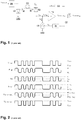
- a typical optical communication system (cf. Fig. 1 : typical optical link; Fig. 2 : typical optical link signalling) comprises three components:
- Such a system typically transmits two-level electrical data pattern V in-data-digital and recovers a replica two-level electrical data pattern V out-data-digital at the receiver side.
- Light (optical) power levels P 1 and P 0 (cf. Fig. 2 ) injected into the light guide GU correspond to each electrical level V HIGH and V LOW . It follows that, at the receiver side, two different light power levels arrive at the input of the light-receiving element PD. These two different light power levels generate two different current levels, namely I 1 and I 0 .
- the current signal I PD generated at the light-receiving element PD has to be converted to a voltage signal.
- An integrator IN in the feedback path FP generates a control signal V int in order to subtract the average input current coming from the light-receiving element PD. This is done in order to generate the zero crossing in the input of a limiter LI.
- the limiter LI acts as a comparator which generates in its output a V HIGH (V LOW ) logic level for positive (negative) voltages in its input.
- the automatic gain control block AG controls the transimpedance amplifier gain R in order to keep the amplitude V out-data-analog to a desired level (for example constant) for different I PD current levels that might occur as input to the transimpedance amplifier TA.
- a status change in the transmitter side could be transmitted to the receiver side. This could be for example a change from EIOS (Electrical Idle Ordered Set - a type of data link layer packet) state to EIEOS (Electric Idle Exit Ordered Set) state in the PCI Express standard.
- EIOS Electrical Idle Ordered Set - a type of data link layer packet
- EIEOS Electrical Idle Exit Ordered Set
- Another optical link could be dedicated to the new signal. However, this is very costly because extra components and extra power is required. Also in some cases, dedicating a complete extra optical link might not be an option at all.
- a third optical power level P 2 different from P 1 and from P 0 is to be transmitted in order to be able to distinguish between the two signals, making a multi-level signalling necessary.
- the object of the present invention is to further develop a circuit arrangement of the above-mentioned type, a corresponding system and a method of the above-mentioned type in such a way that an optical receiver is adapted to receive multilevel optical signals resulting from the superposition of high speed data signals and low speed data signals.
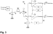
- a circuit arrangement for receiving multilevel optical signals from at least one optical guide, said multilevel optical signals comprising high-speed data signals and low-speed status signals comprises:
- the circuit arrangement works according to the following method for receiving multilevel optical signals from at least one optical guide, said multilevel optical signals comprising high-speed data signals and low-speed status signals, said method comprising the steps of:
- the second limiter is assigned to the second transimpedance amplifier and to the automatic offset controller.
- the automatic gain controller sets the same gain or same transimpedance for both the transimpedance amplifier and the second transimpedance amplifier by sensing the amplitude of the output of the transimpedance amplifier.
- At least one peak detector circuit is provided for sensing the amplitude of the output of the transimpedance amplifier.
- the peak detector circuit is part of the automatic gain control or is shared between the automatic gain controller and the automatic offset controller.
- the amplitude of the output of the transimpedance amplifier is provided to the input of the automatic offset controller.
- the transimpedance amplifier is at least one multi-stage amplifier.
- the second transimpedance amplifier is at least one multi-stage amplifier.
- a short is arranged between the output node of the first stage of the transimpedance amplifier and the output node of the first stage of the second transimpedance amplifier.
- the light-receiving component is at least one photodetector, in particular at least one photodiode.
- the optical guide is at least one fibre.
- the end of the optical guide which is not assigned to the light-receiving component, is assigned to at least one light-emitting component, which is preceded by at least one driver for converting electrical data logic levels into the optical signals.
- the present invention finally relates to the use of at least one circuit arrangement according to the type presented hereinbefore and/or of the method according to the type presented hereinbefore for the optical transmission of data signals and of status signals.
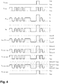
- V in-status-digital is inputted on the transmitter side.
- V in-status-digital is a slow signal comprising short pulses widely spaced-in-time.
- the transition rate of V in-status-digital is significantly low compared to the transition rate of V in-data-digital .
- the optical power P 2 is chosen to be higher than P 1 , such that the received currents I 2 and I 1 fulfill the relation I 2 ⁇ 2*I 1 .
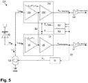
- the second transimpedance amplifier TA2 can be a copy of the transimpedance amplifier TA, or the second transimpedance amplifier TA2 can be an exactly scaled version of the transimpedance amplifier TA.
- the automatic gain control block AG sets the same gain or same transimpedance R for both the transimpedance amplifier TA and the second transimpedance amplifier TA2 by sensing only the V out-data-analog amplitude with of a peak detector circuit, which can be part of the automatic gain control AG or can be shared between the automatic gain control AG and an automatic offset control AO.
- the automatic offset control AO sets the voltage V offset for the second transimpedance amplifier TA2; for example, V offset can be R*(I 1 -I 0 )/2.
- V offset can be R*(I 1 -I 0 )/2.
- the value of V offset is independent of I 2 , and the information about its value is extracted only from V out-data-analog .
- V offset R*(I 1 -I 0 )/2 is achieved by setting V offset double the amplitude.
- V out-data-analog can be measured with a peak detector circuit.
- the peak detector circuit can be part of the automatic offset control AO or can be shared between the automatic offset control AO and the automatic gain control AG.
- V out-status-analog is used as the feedback signal for the automatic offset control block AO because the V out-status-analog average value is -V offset .
- the averaging circuit is part of the automatic offset control block AO.
- the link operation during an initial phase, only the high speed V in-data-digital signal is transmitted.
- the V in-status-digital signal is kept low during this phase.
- the automatic gain control AG and the automatic offset control AO outputs settle to their final value.
- the time constant of these two loops is significantly lower than the time distance between the two consecutive pulses on the V in-status-digital signal.
- V in-status-digital Only after this first initial phase the V in-status-digital signal can be transmitted.
- the V in-status-digital signal When the V in-status-digital signal is low, the V out-data-digital signal follows the V in-data-digital signal.
- the optical power transmitted is always P 2 , independently of the value of the V in-data-digital signal.
- V out-data-digital will be high independently of the value of V in-data-digital .
- the V out-status-digital goes high as well.
- a short between the output nodes of the first stage of the first transimpedance amplifier TA and of the first stage of the second transimpedance amplifier TA2 can be provided, as depicted in Fig. 5 .
- the slow speed signal can be reliably transmitted by sharing the same physical optical link and using multilevel signalling.
Landscapes
- Engineering & Computer Science (AREA)
- Physics & Mathematics (AREA)
- Computer Networks & Wireless Communication (AREA)
- Signal Processing (AREA)
- Electromagnetism (AREA)
- Power Engineering (AREA)
- Amplifiers (AREA)
- Optical Communication System (AREA)
- Light Receiving Elements (AREA)
- Spectroscopy & Molecular Physics (AREA)
- Control Of Amplification And Gain Control (AREA)
Priority Applications (1)
| Application Number | Priority Date | Filing Date | Title |
|---|---|---|---|
| EP14722633.6A EP2992628B1 (en) | 2013-04-30 | 2014-04-30 | Circuit arrangement and method for receiving optical signals |
Applications Claiming Priority (3)
| Application Number | Priority Date | Filing Date | Title |
|---|---|---|---|
| EP13166092 | 2013-04-30 | ||
| EP14722633.6A EP2992628B1 (en) | 2013-04-30 | 2014-04-30 | Circuit arrangement and method for receiving optical signals |
| PCT/EP2014/058937 WO2014177665A1 (en) | 2013-04-30 | 2014-04-30 | Circuit arrangement and method for receiving optical signals |
Publications (2)
| Publication Number | Publication Date |
|---|---|
| EP2992628A1 EP2992628A1 (en) | 2016-03-09 |
| EP2992628B1 true EP2992628B1 (en) | 2018-10-31 |
Family
ID=48463700
Family Applications (1)
| Application Number | Title | Priority Date | Filing Date |
|---|---|---|---|
| EP14722633.6A Active EP2992628B1 (en) | 2013-04-30 | 2014-04-30 | Circuit arrangement and method for receiving optical signals |
Country Status (4)
| Country | Link |
|---|---|
| US (1) | US9780886B2 (enExample) |
| EP (1) | EP2992628B1 (enExample) |
| JP (1) | JP6437530B2 (enExample) |
| WO (1) | WO2014177665A1 (enExample) |
Cited By (1)
| Publication number | Priority date | Publication date | Assignee | Title |
|---|---|---|---|---|
| TWI866046B (zh) * | 2022-02-02 | 2024-12-11 | 美商陞特有限公司 | 轉阻放大器裝置以及光接收器 |
Families Citing this family (3)
| Publication number | Priority date | Publication date | Assignee | Title |
|---|---|---|---|---|
| US10782339B2 (en) * | 2016-04-29 | 2020-09-22 | Teradyne, Inc. | Method and test system for providing accurate analog signals |
| CN107980208B (zh) * | 2017-10-19 | 2021-08-13 | 深圳市汇顶科技股份有限公司 | 信号转换电路、心率传感器和电子设备 |
| US10715358B1 (en) * | 2018-11-29 | 2020-07-14 | Xilinx, Inc. | Circuit for and method of receiving signals in an integrated circuit device |
Family Cites Families (14)
| Publication number | Priority date | Publication date | Assignee | Title |
|---|---|---|---|---|
| GB2175480B (en) * | 1985-05-21 | 1988-12-29 | Stc Plc | Demodulation of auxiliary low frequency channels in digital transmission systems |
| DE3544393A1 (de) * | 1985-12-16 | 1987-06-19 | Philips Patentverwaltung | Diensteintegrierendes, digitales nachrichtenuebertragungssystem mit einrichtungen zur gemeinsamen uebertragung von schmalband- und breitbandsignalen |
| FR2630871B1 (fr) * | 1988-04-29 | 1994-03-18 | Alcatel Cit | Procede et dispositif d'adjonction et de separation d'un canal numerique a bas debit au canal numerique a haut debit d'une liaison de transmission |
| US6763060B1 (en) * | 1999-02-19 | 2004-07-13 | Oasis Silicon Systems | Communication system employing a network of power managed transceivers that can generate a clocking signal or enable data bypass of a digital system associated with each transceiver |
| EP1357682A1 (en) * | 2002-04-23 | 2003-10-29 | Agilent Technologies, Inc. - a Delaware corporation - | Module apparatus for optical communication and circuit pack therefor |
| US6894568B2 (en) * | 2003-08-20 | 2005-05-17 | Intel Corporation | Transimpedance amplifier with receive signal strength indicator |
| US7406268B2 (en) * | 2003-08-27 | 2008-07-29 | Avago Technologies Limited | Optical receiver circuit |
| WO2006013893A1 (ja) * | 2004-08-03 | 2006-02-09 | Nippon Telegraph And Telephone Corporation | トランスインピーダンスアンプ |
| US20060216042A1 (en) * | 2005-03-24 | 2006-09-28 | Yeo Kok S | Automatic gain control circuit for infrared receiver |
| JP4927664B2 (ja) * | 2007-08-14 | 2012-05-09 | 日本電信電話株式会社 | 前置増幅回路 |
| US8983308B2 (en) * | 2009-09-22 | 2015-03-17 | Calix, Inc. | Optical network device with multi-transport support |
| US8155538B2 (en) * | 2009-12-09 | 2012-04-10 | Oracle America, Inc. | Technique for calibrating and centering an optical receiver |
| US8238761B2 (en) * | 2009-12-09 | 2012-08-07 | Oracle America, Inc. | Optical receiver with a calibration mode |
| JP5861363B2 (ja) * | 2011-09-30 | 2016-02-16 | 住友電気工業株式会社 | 増幅装置 |
-
2014
- 2014-04-30 WO PCT/EP2014/058937 patent/WO2014177665A1/en not_active Ceased
- 2014-04-30 EP EP14722633.6A patent/EP2992628B1/en active Active
- 2014-04-30 JP JP2016511081A patent/JP6437530B2/ja not_active Expired - Fee Related
-
2015
- 2015-10-29 US US14/926,862 patent/US9780886B2/en active Active
Non-Patent Citations (1)
| Title |
|---|
| None * |
Cited By (2)
| Publication number | Priority date | Publication date | Assignee | Title |
|---|---|---|---|---|
| TWI866046B (zh) * | 2022-02-02 | 2024-12-11 | 美商陞特有限公司 | 轉阻放大器裝置以及光接收器 |
| US12224718B2 (en) | 2022-02-02 | 2025-02-11 | Semtech Corporation | Transimpedance amplifiers |
Also Published As
| Publication number | Publication date |
|---|---|
| JP6437530B2 (ja) | 2018-12-12 |
| US9780886B2 (en) | 2017-10-03 |
| EP2992628A1 (en) | 2016-03-09 |
| WO2014177665A8 (en) | 2015-06-11 |
| WO2014177665A1 (en) | 2014-11-06 |
| US20160050026A1 (en) | 2016-02-18 |
| JP2016524366A (ja) | 2016-08-12 |
Similar Documents
| Publication | Publication Date | Title |
|---|---|---|
| TWI514789B (zh) | 用於建立及改良一通訊鏈路之方法及用於高速通訊之方法 | |
| US10122469B2 (en) | Optical transmitter, active optical cable, and optical transmission method | |
| US20110299858A1 (en) | Host device with multipurpose optics drive capabilities | |
| EP2992628B1 (en) | Circuit arrangement and method for receiving optical signals | |
| US20020027689A1 (en) | Fiber optic transceiver employing front end level control | |
| AU2005316460A1 (en) | System and method for optically powering a remote network component | |
| KR101557218B1 (ko) | 수직 공진 표면 방출 레이저 다이오드 구동 장치 및 구동 방법 | |
| JP5172046B1 (ja) | 親局側装置 | |
| US10469173B2 (en) | High-speed low-power-consumption optical transceiver chip | |
| CN104426611B (zh) | 低频ac比较电路和包括其的光学模块 | |
| US9882651B2 (en) | Methods, circuits and optical cable assemblies for optical transmission of high-speed data and low-speed data | |
| US10461882B2 (en) | Optical network unit for optical transmission in burst mode | |
| CN102598542A (zh) | 量化光电子模块中的链路质量 | |
| CN1426180A (zh) | 光波长/模式转换器 | |
| KR102017881B1 (ko) | 변조 방식 가변형 광 송수신기 | |
| JP2012249284A (ja) | Vcselベースの光通信リンクを制御する方法及び装置 | |
| CN101854211B (zh) | 高速单纤双向光模块 | |
| US9621972B2 (en) | Burst-mode receiver | |
| KR101411746B1 (ko) | 잡음 제거 방법 및 광송수신기 | |
| US6469823B2 (en) | Optical wavelength converter and optical wavelength division multiplexing communication system using the same | |
| US12126384B2 (en) | Optical transmitter and method for controlling optical transmitter | |
| CN109617609A (zh) | 一种工业级10g高速光收发模块 | |
| CN116961766A (zh) | 一种发射电路、光模块和通信设备 | |
| KR20110067777A (ko) | 광송수신 제어장치 | |
| CN110995353B (zh) | 一种宽带模拟调制的激光收发模块及控制方法 |
Legal Events
| Date | Code | Title | Description |
|---|---|---|---|
| PUAI | Public reference made under article 153(3) epc to a published international application that has entered the european phase |
Free format text: ORIGINAL CODE: 0009012 |
|
| 17P | Request for examination filed |
Effective date: 20151130 |
|
| AK | Designated contracting states |
Kind code of ref document: A1 Designated state(s): AL AT BE BG CH CY CZ DE DK EE ES FI FR GB GR HR HU IE IS IT LI LT LU LV MC MK MT NL NO PL PT RO RS SE SI SK SM TR |
|
| AX | Request for extension of the european patent |
Extension state: BA ME |
|
| RAP1 | Party data changed (applicant data changed or rights of an application transferred) |
Owner name: SILICON LINE GMBH |
|
| RIN1 | Information on inventor provided before grant (corrected) |
Inventor name: HIDRI, OLS Inventor name: GROEPL, MARTIN Inventor name: HOELTKE, HOLGER |
|
| DAX | Request for extension of the european patent (deleted) | ||
| STAA | Information on the status of an ep patent application or granted ep patent |
Free format text: STATUS: EXAMINATION IS IN PROGRESS |
|
| 17Q | First examination report despatched |
Effective date: 20170907 |
|
| GRAP | Despatch of communication of intention to grant a patent |
Free format text: ORIGINAL CODE: EPIDOSNIGR1 |
|
| STAA | Information on the status of an ep patent application or granted ep patent |
Free format text: STATUS: GRANT OF PATENT IS INTENDED |
|
| INTG | Intention to grant announced |
Effective date: 20180511 |
|
| GRAS | Grant fee paid |
Free format text: ORIGINAL CODE: EPIDOSNIGR3 |
|
| GRAA | (expected) grant |
Free format text: ORIGINAL CODE: 0009210 |
|
| STAA | Information on the status of an ep patent application or granted ep patent |
Free format text: STATUS: THE PATENT HAS BEEN GRANTED |
|
| AK | Designated contracting states |
Kind code of ref document: B1 Designated state(s): AL AT BE BG CH CY CZ DE DK EE ES FI FR GB GR HR HU IE IS IT LI LT LU LV MC MK MT NL NO PL PT RO RS SE SI SK SM TR |
|
| REG | Reference to a national code |
Ref country code: CH Ref legal event code: EP Ref country code: GB Ref legal event code: FG4D |
|
| REG | Reference to a national code |
Ref country code: AT Ref legal event code: REF Ref document number: 1060661 Country of ref document: AT Kind code of ref document: T Effective date: 20181115 |
|
| REG | Reference to a national code |
Ref country code: DE Ref legal event code: R096 Ref document number: 602014035083 Country of ref document: DE |
|
| REG | Reference to a national code |
Ref country code: IE Ref legal event code: FG4D |
|
| REG | Reference to a national code |
Ref country code: NL Ref legal event code: MP Effective date: 20181031 |
|
| REG | Reference to a national code |
Ref country code: LT Ref legal event code: MG4D |
|
| REG | Reference to a national code |
Ref country code: AT Ref legal event code: MK05 Ref document number: 1060661 Country of ref document: AT Kind code of ref document: T Effective date: 20181031 |
|
| PG25 | Lapsed in a contracting state [announced via postgrant information from national office to epo] |
Ref country code: FI Free format text: LAPSE BECAUSE OF FAILURE TO SUBMIT A TRANSLATION OF THE DESCRIPTION OR TO PAY THE FEE WITHIN THE PRESCRIBED TIME-LIMIT Effective date: 20181031 Ref country code: LV Free format text: LAPSE BECAUSE OF FAILURE TO SUBMIT A TRANSLATION OF THE DESCRIPTION OR TO PAY THE FEE WITHIN THE PRESCRIBED TIME-LIMIT Effective date: 20181031 Ref country code: HR Free format text: LAPSE BECAUSE OF FAILURE TO SUBMIT A TRANSLATION OF THE DESCRIPTION OR TO PAY THE FEE WITHIN THE PRESCRIBED TIME-LIMIT Effective date: 20181031 Ref country code: LT Free format text: LAPSE BECAUSE OF FAILURE TO SUBMIT A TRANSLATION OF THE DESCRIPTION OR TO PAY THE FEE WITHIN THE PRESCRIBED TIME-LIMIT Effective date: 20181031 Ref country code: BG Free format text: LAPSE BECAUSE OF FAILURE TO SUBMIT A TRANSLATION OF THE DESCRIPTION OR TO PAY THE FEE WITHIN THE PRESCRIBED TIME-LIMIT Effective date: 20190131 Ref country code: AT Free format text: LAPSE BECAUSE OF FAILURE TO SUBMIT A TRANSLATION OF THE DESCRIPTION OR TO PAY THE FEE WITHIN THE PRESCRIBED TIME-LIMIT Effective date: 20181031 Ref country code: PL Free format text: LAPSE BECAUSE OF FAILURE TO SUBMIT A TRANSLATION OF THE DESCRIPTION OR TO PAY THE FEE WITHIN THE PRESCRIBED TIME-LIMIT Effective date: 20181031 Ref country code: IS Free format text: LAPSE BECAUSE OF FAILURE TO SUBMIT A TRANSLATION OF THE DESCRIPTION OR TO PAY THE FEE WITHIN THE PRESCRIBED TIME-LIMIT Effective date: 20190228 Ref country code: ES Free format text: LAPSE BECAUSE OF FAILURE TO SUBMIT A TRANSLATION OF THE DESCRIPTION OR TO PAY THE FEE WITHIN THE PRESCRIBED TIME-LIMIT Effective date: 20181031 Ref country code: NO Free format text: LAPSE BECAUSE OF FAILURE TO SUBMIT A TRANSLATION OF THE DESCRIPTION OR TO PAY THE FEE WITHIN THE PRESCRIBED TIME-LIMIT Effective date: 20190131 |
|
| PG25 | Lapsed in a contracting state [announced via postgrant information from national office to epo] |
Ref country code: NL Free format text: LAPSE BECAUSE OF FAILURE TO SUBMIT A TRANSLATION OF THE DESCRIPTION OR TO PAY THE FEE WITHIN THE PRESCRIBED TIME-LIMIT Effective date: 20181031 Ref country code: PT Free format text: LAPSE BECAUSE OF FAILURE TO SUBMIT A TRANSLATION OF THE DESCRIPTION OR TO PAY THE FEE WITHIN THE PRESCRIBED TIME-LIMIT Effective date: 20190301 Ref country code: RS Free format text: LAPSE BECAUSE OF FAILURE TO SUBMIT A TRANSLATION OF THE DESCRIPTION OR TO PAY THE FEE WITHIN THE PRESCRIBED TIME-LIMIT Effective date: 20181031 Ref country code: SE Free format text: LAPSE BECAUSE OF FAILURE TO SUBMIT A TRANSLATION OF THE DESCRIPTION OR TO PAY THE FEE WITHIN THE PRESCRIBED TIME-LIMIT Effective date: 20181031 Ref country code: AL Free format text: LAPSE BECAUSE OF FAILURE TO SUBMIT A TRANSLATION OF THE DESCRIPTION OR TO PAY THE FEE WITHIN THE PRESCRIBED TIME-LIMIT Effective date: 20181031 Ref country code: GR Free format text: LAPSE BECAUSE OF FAILURE TO SUBMIT A TRANSLATION OF THE DESCRIPTION OR TO PAY THE FEE WITHIN THE PRESCRIBED TIME-LIMIT Effective date: 20190201 |
|
| PG25 | Lapsed in a contracting state [announced via postgrant information from national office to epo] |
Ref country code: IT Free format text: LAPSE BECAUSE OF FAILURE TO SUBMIT A TRANSLATION OF THE DESCRIPTION OR TO PAY THE FEE WITHIN THE PRESCRIBED TIME-LIMIT Effective date: 20181031 Ref country code: CZ Free format text: LAPSE BECAUSE OF FAILURE TO SUBMIT A TRANSLATION OF THE DESCRIPTION OR TO PAY THE FEE WITHIN THE PRESCRIBED TIME-LIMIT Effective date: 20181031 Ref country code: DK Free format text: LAPSE BECAUSE OF FAILURE TO SUBMIT A TRANSLATION OF THE DESCRIPTION OR TO PAY THE FEE WITHIN THE PRESCRIBED TIME-LIMIT Effective date: 20181031 |
|
| REG | Reference to a national code |
Ref country code: DE Ref legal event code: R097 Ref document number: 602014035083 Country of ref document: DE |
|
| PG25 | Lapsed in a contracting state [announced via postgrant information from national office to epo] |
Ref country code: SM Free format text: LAPSE BECAUSE OF FAILURE TO SUBMIT A TRANSLATION OF THE DESCRIPTION OR TO PAY THE FEE WITHIN THE PRESCRIBED TIME-LIMIT Effective date: 20181031 Ref country code: EE Free format text: LAPSE BECAUSE OF FAILURE TO SUBMIT A TRANSLATION OF THE DESCRIPTION OR TO PAY THE FEE WITHIN THE PRESCRIBED TIME-LIMIT Effective date: 20181031 Ref country code: SK Free format text: LAPSE BECAUSE OF FAILURE TO SUBMIT A TRANSLATION OF THE DESCRIPTION OR TO PAY THE FEE WITHIN THE PRESCRIBED TIME-LIMIT Effective date: 20181031 Ref country code: RO Free format text: LAPSE BECAUSE OF FAILURE TO SUBMIT A TRANSLATION OF THE DESCRIPTION OR TO PAY THE FEE WITHIN THE PRESCRIBED TIME-LIMIT Effective date: 20181031 |
|
| PLBE | No opposition filed within time limit |
Free format text: ORIGINAL CODE: 0009261 |
|
| STAA | Information on the status of an ep patent application or granted ep patent |
Free format text: STATUS: NO OPPOSITION FILED WITHIN TIME LIMIT |
|
| 26N | No opposition filed |
Effective date: 20190801 |
|
| PG25 | Lapsed in a contracting state [announced via postgrant information from national office to epo] |
Ref country code: SI Free format text: LAPSE BECAUSE OF FAILURE TO SUBMIT A TRANSLATION OF THE DESCRIPTION OR TO PAY THE FEE WITHIN THE PRESCRIBED TIME-LIMIT Effective date: 20181031 |
|
| PG25 | Lapsed in a contracting state [announced via postgrant information from national office to epo] |
Ref country code: MC Free format text: LAPSE BECAUSE OF FAILURE TO SUBMIT A TRANSLATION OF THE DESCRIPTION OR TO PAY THE FEE WITHIN THE PRESCRIBED TIME-LIMIT Effective date: 20181031 Ref country code: LU Free format text: LAPSE BECAUSE OF NON-PAYMENT OF DUE FEES Effective date: 20190430 |
|
| PG25 | Lapsed in a contracting state [announced via postgrant information from national office to epo] |
Ref country code: TR Free format text: LAPSE BECAUSE OF FAILURE TO SUBMIT A TRANSLATION OF THE DESCRIPTION OR TO PAY THE FEE WITHIN THE PRESCRIBED TIME-LIMIT Effective date: 20181031 |
|
| PG25 | Lapsed in a contracting state [announced via postgrant information from national office to epo] |
Ref country code: IE Free format text: LAPSE BECAUSE OF NON-PAYMENT OF DUE FEES Effective date: 20190430 |
|
| PG25 | Lapsed in a contracting state [announced via postgrant information from national office to epo] |
Ref country code: CY Free format text: LAPSE BECAUSE OF FAILURE TO SUBMIT A TRANSLATION OF THE DESCRIPTION OR TO PAY THE FEE WITHIN THE PRESCRIBED TIME-LIMIT Effective date: 20181031 |
|
| PG25 | Lapsed in a contracting state [announced via postgrant information from national office to epo] |
Ref country code: MT Free format text: LAPSE BECAUSE OF FAILURE TO SUBMIT A TRANSLATION OF THE DESCRIPTION OR TO PAY THE FEE WITHIN THE PRESCRIBED TIME-LIMIT Effective date: 20181031 Ref country code: HU Free format text: LAPSE BECAUSE OF FAILURE TO SUBMIT A TRANSLATION OF THE DESCRIPTION OR TO PAY THE FEE WITHIN THE PRESCRIBED TIME-LIMIT; INVALID AB INITIO Effective date: 20140430 |
|
| PGFP | Annual fee paid to national office [announced via postgrant information from national office to epo] |
Ref country code: CH Payment date: 20210731 Year of fee payment: 8 |
|
| PG25 | Lapsed in a contracting state [announced via postgrant information from national office to epo] |
Ref country code: MK Free format text: LAPSE BECAUSE OF FAILURE TO SUBMIT A TRANSLATION OF THE DESCRIPTION OR TO PAY THE FEE WITHIN THE PRESCRIBED TIME-LIMIT Effective date: 20181031 |
|
| REG | Reference to a national code |
Ref country code: CH Ref legal event code: PL |
|
| PG25 | Lapsed in a contracting state [announced via postgrant information from national office to epo] |
Ref country code: LI Free format text: LAPSE BECAUSE OF NON-PAYMENT OF DUE FEES Effective date: 20220430 Ref country code: CH Free format text: LAPSE BECAUSE OF NON-PAYMENT OF DUE FEES Effective date: 20220430 |
|
| P01 | Opt-out of the competence of the unified patent court (upc) registered |
Effective date: 20230527 |
|
| PGFP | Annual fee paid to national office [announced via postgrant information from national office to epo] |
Ref country code: BE Payment date: 20230427 Year of fee payment: 10 |
|
| PGFP | Annual fee paid to national office [announced via postgrant information from national office to epo] |
Ref country code: GB Payment date: 20230531 Year of fee payment: 10 |
|
| GBPC | Gb: european patent ceased through non-payment of renewal fee |
Effective date: 20240430 |
|
| REG | Reference to a national code |
Ref country code: BE Ref legal event code: MM Effective date: 20240430 |
|
| PG25 | Lapsed in a contracting state [announced via postgrant information from national office to epo] |
Ref country code: BE Free format text: LAPSE BECAUSE OF NON-PAYMENT OF DUE FEES Effective date: 20240430 |
|
| PG25 | Lapsed in a contracting state [announced via postgrant information from national office to epo] |
Ref country code: GB Free format text: LAPSE BECAUSE OF NON-PAYMENT OF DUE FEES Effective date: 20240430 |
|
| PG25 | Lapsed in a contracting state [announced via postgrant information from national office to epo] |
Ref country code: GB Free format text: LAPSE BECAUSE OF NON-PAYMENT OF DUE FEES Effective date: 20240430 Ref country code: BE Free format text: LAPSE BECAUSE OF NON-PAYMENT OF DUE FEES Effective date: 20240430 |
|
| PGFP | Annual fee paid to national office [announced via postgrant information from national office to epo] |
Ref country code: FR Payment date: 20250430 Year of fee payment: 12 |
|
| PGFP | Annual fee paid to national office [announced via postgrant information from national office to epo] |
Ref country code: DE Payment date: 20250630 Year of fee payment: 12 |