EP2991465A1 - Electronic control device - Google Patents
Electronic control device Download PDFInfo
- Publication number
- EP2991465A1 EP2991465A1 EP14789081.8A EP14789081A EP2991465A1 EP 2991465 A1 EP2991465 A1 EP 2991465A1 EP 14789081 A EP14789081 A EP 14789081A EP 2991465 A1 EP2991465 A1 EP 2991465A1
- Authority
- EP
- European Patent Office
- Prior art keywords
- wiring
- electronic component
- center line
- land
- line extending
- Prior art date
- Legal status (The legal status is an assumption and is not a legal conclusion. Google has not performed a legal analysis and makes no representation as to the accuracy of the status listed.)
- Granted
Links
Images









Classifications
-
- H—ELECTRICITY
- H05—ELECTRIC TECHNIQUES NOT OTHERWISE PROVIDED FOR
- H05K—PRINTED CIRCUITS; CASINGS OR CONSTRUCTIONAL DETAILS OF ELECTRIC APPARATUS; MANUFACTURE OF ASSEMBLAGES OF ELECTRICAL COMPONENTS
- H05K1/00—Printed circuits
- H05K1/18—Printed circuits structurally associated with non-printed electric components
- H05K1/181—Printed circuits structurally associated with non-printed electric components associated with surface mounted components
-
- H—ELECTRICITY
- H05—ELECTRIC TECHNIQUES NOT OTHERWISE PROVIDED FOR
- H05K—PRINTED CIRCUITS; CASINGS OR CONSTRUCTIONAL DETAILS OF ELECTRIC APPARATUS; MANUFACTURE OF ASSEMBLAGES OF ELECTRICAL COMPONENTS
- H05K3/00—Apparatus or processes for manufacturing printed circuits
- H05K3/30—Assembling printed circuits with electric components, e.g. with resistors
- H05K3/32—Assembling printed circuits with electric components, e.g. with resistors electrically connecting electric components or wires to printed circuits
- H05K3/34—Assembling printed circuits with electric components, e.g. with resistors electrically connecting electric components or wires to printed circuits by soldering
- H05K3/341—Surface mounted components
- H05K3/3431—Leadless components
- H05K3/3442—Leadless components having edge contacts, e.g. leadless chip capacitors, chip carriers
-
- H—ELECTRICITY
- H05—ELECTRIC TECHNIQUES NOT OTHERWISE PROVIDED FOR
- H05K—PRINTED CIRCUITS; CASINGS OR CONSTRUCTIONAL DETAILS OF ELECTRIC APPARATUS; MANUFACTURE OF ASSEMBLAGES OF ELECTRICAL COMPONENTS
- H05K1/00—Printed circuits
- H05K1/02—Details
- H05K1/11—Printed elements for providing electric connections to or between printed circuits
- H05K1/111—Pads for surface mounting, e.g. lay-out
-
- H—ELECTRICITY
- H05—ELECTRIC TECHNIQUES NOT OTHERWISE PROVIDED FOR
- H05K—PRINTED CIRCUITS; CASINGS OR CONSTRUCTIONAL DETAILS OF ELECTRIC APPARATUS; MANUFACTURE OF ASSEMBLAGES OF ELECTRICAL COMPONENTS
- H05K2201/00—Indexing scheme relating to printed circuits covered by H05K1/00
- H05K2201/09—Shape and layout
- H05K2201/09209—Shape and layout details of conductors
- H05K2201/09372—Pads and lands
- H05K2201/09381—Shape of non-curved single flat metallic pad, land or exposed part thereof; Shape of electrode of leadless component
-
- H—ELECTRICITY
- H05—ELECTRIC TECHNIQUES NOT OTHERWISE PROVIDED FOR
- H05K—PRINTED CIRCUITS; CASINGS OR CONSTRUCTIONAL DETAILS OF ELECTRIC APPARATUS; MANUFACTURE OF ASSEMBLAGES OF ELECTRICAL COMPONENTS
- H05K2201/00—Indexing scheme relating to printed circuits covered by H05K1/00
- H05K2201/09—Shape and layout
- H05K2201/09209—Shape and layout details of conductors
- H05K2201/09372—Pads and lands
- H05K2201/09427—Special relation between the location or dimension of a pad or land and the location or dimension of a terminal
-
- H—ELECTRICITY
- H05—ELECTRIC TECHNIQUES NOT OTHERWISE PROVIDED FOR
- H05K—PRINTED CIRCUITS; CASINGS OR CONSTRUCTIONAL DETAILS OF ELECTRIC APPARATUS; MANUFACTURE OF ASSEMBLAGES OF ELECTRICAL COMPONENTS
- H05K2201/00—Indexing scheme relating to printed circuits covered by H05K1/00
- H05K2201/09—Shape and layout
- H05K2201/09209—Shape and layout details of conductors
- H05K2201/09654—Shape and layout details of conductors covering at least two types of conductors provided for in H05K2201/09218 - H05K2201/095
- H05K2201/09663—Divided layout, i.e. conductors divided in two or more parts
-
- H—ELECTRICITY
- H05—ELECTRIC TECHNIQUES NOT OTHERWISE PROVIDED FOR
- H05K—PRINTED CIRCUITS; CASINGS OR CONSTRUCTIONAL DETAILS OF ELECTRIC APPARATUS; MANUFACTURE OF ASSEMBLAGES OF ELECTRICAL COMPONENTS
- H05K2201/00—Indexing scheme relating to printed circuits covered by H05K1/00
- H05K2201/10—Details of components or other objects attached to or integrated in a printed circuit board
- H05K2201/10613—Details of electrical connections of non-printed components, e.g. special leads
- H05K2201/10621—Components characterised by their electrical contacts
- H05K2201/10636—Leadless chip, e.g. chip capacitor or resistor
-
- Y—GENERAL TAGGING OF NEW TECHNOLOGICAL DEVELOPMENTS; GENERAL TAGGING OF CROSS-SECTIONAL TECHNOLOGIES SPANNING OVER SEVERAL SECTIONS OF THE IPC; TECHNICAL SUBJECTS COVERED BY FORMER USPC CROSS-REFERENCE ART COLLECTIONS [XRACs] AND DIGESTS
- Y02—TECHNOLOGIES OR APPLICATIONS FOR MITIGATION OR ADAPTATION AGAINST CLIMATE CHANGE
- Y02P—CLIMATE CHANGE MITIGATION TECHNOLOGIES IN THE PRODUCTION OR PROCESSING OF GOODS
- Y02P70/00—Climate change mitigation technologies in the production process for final industrial or consumer products
- Y02P70/50—Manufacturing or production processes characterised by the final manufactured product
Definitions
- the present invention relates to an electronic control device including a circuit wiring board in which an electronic component is connected to a land.
- Such electronic control device On a vehicle such as an automobile, various electronic control devices for engine control, for motor control, for automatic transmission control, and the like for example are mounted.
- the electronic control device there is one including a MOSFET for switching an inverter device, a DC-DC converter device, and the like, a capacitor module, and the like.
- Such electronic control device includes a circuit wiring board having plural solid wiring patterns and a chip component in which the electrodes formed in both ends are soldered to the wiring patterns.
- an electronic control device for a vehicle is installed under an environment with sharp temperature change, solid wiring patterns and a chip component repeat expansion and shrinkage, and a crack is liable to occur in solder that connects the chip component and the wiring patterns to each other.
- a surface mounting structure in which lands soldered to the electrodes of the chip component and wiring that connects the lands and the wiring patterns to each other are arranged in a circuit wiring board.
- the connection part of each land and the wiring is disposed within a region in which the region of the width of the chip component extends in the longitudinal direction or within a region in which the region of the length of the chip component extends in the transverse direction (refer to FIG. 1(a) of Patent Literature 1 for example).
- Patent Literature 1 JP-A-2008-72065
- connection portion of each land and the wiring is disposed within a region in which the region of the width of the chip component extends in the longitudinal direction or within a region in which the region of the length of the chip component extends in the transverse direction.
- the distances from the wiring to the solder connection portions connected to both side surfaces of the chip component are generally equal to each other. Therefore, a large stress is generated in both sides in the width direction of the solder connection portion formed on the land, and the crack is liable to occur in both sides in the width direction of this solder connection portion formed on the land.
- An electronic control device of the present invention includes a circuit wiring board in which a wiring pattern is formed on a base metal, with the wiring pattern including a pair of patterns having a large area, a pair of lands arranged between the pair of patterns at a predetermined interval and having an area smaller than that of the pattern, and a pair of wiring portions connecting the pair of lands and the pair of patterns respectively, and an electronic component in which electrodes having a predetermined length and a predetermined width and arranged in one end and the other end in the longitudinal direction respectively are connected to the respective lands respectively, in which the wiring portions are arranged so that the center in the width direction of the connection portion connected to the land is disposed at a position that is outside of both a region in which a region of the predetermined width of the electronic component extends in the longitudinal direction of the electronic component and a region in which a region of the predetermined length of the electronic component extends in the transverse direction of the electronic component.
- the length to the point where the wire breakage caused by the crack of the solder occurs becomes long, the lifetime until the wire breakage can be made long, and the reliability can be improved.
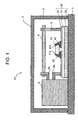
- FIG. 1 is a cross-sectional view of an electronic control device 10
- FIG. 2 is an enlarged cross-sectional view of a circuit wiring board illustrated in FIG. 1 on which a chip component is mounted.
- the electronic control device 10 illustrated in FIG. 1 is used for engine control, motor control, automatic transmission control, and the like of a vehicle such as an automobile for example.
- the electronic control device 10 includes a case 3 formed of a case base portion 1 and a case cover portion 2 that seals the case base portion 1. Inside the case 3, a circuit wire board 30, a chip component (electronic component) 41 mounted on the circuit wire board 30, a capacitor module 6, a circuit board for control 4, and a conductor 5 such as a bus bar are stored.
- the case base portion 1 and the case cover portion 2 are formed of a metal having a main composition of aluminum, iron and copper, a ceramic, or a resin such as a glass epoxy resin, are fixed by a fastening member and the like not illustrated through a seal member not illustrated, and construct a sealing structure.
- the capacitor module 6 is formed by storing X-capacitors imposed between the phases and Y-capacitors imposed between each phase and a chassis within a capacitor case, and flattens the noise inputted to the circuit board for control 4.
- One electrode 6a of the capacitor module 6 is connected to the circuit board for control 4, and the other electrode 6b is connected to the circuit wiring board 30.
- the circuit board for control 4 and the circuit wiring board 30 are connected to each other by the conductor 5.
- the circuit wiring board 30 includes a base board 38 formed of a metal having the main composition of aluminum, iron and copper or a resin, an insulation layer 37 formed on one surface of the base board 38, and plural wiring patterns 31 formed on the insulation layer 37.
- the chip component 41 is a passive element such as a capacitor and a resistor, and includes a pair of electrodes 41a, 41b on both end sides.
- the electrodes 41a, 41b are mounted on lands 33a, 33b (refer to FIG. 3 ) of the wiring patterns 31 respectively, and are soldered by solder 42.
- the solder 42 is formed of a material not containing lead (lead-free) such as SnAgCu for example.
- FIG. 3 (a) is a plan view of the wiring pattern 31 illustrated in FIG. 2 on which the chip component 41 is mounted as viewed from the top
- FIG. 3 (b) is an enlarged view of the region IIIb of FIG. 3 (a) .
- a number of wiring patterns are formed to which an active component such as a MOSFET for switching and a number of chip components are connected, however, below, one chip component 41 and a pair of wiring patterns 31A, 31B to which this chip component is soldered will be explained.
- the reference sign Xo is a straight line extending in the y-direction and passing through the center O of the chip component 41, and is referred to as the center line Xo in the present description.
- the reference sign Yo is a straight line extending in the x-direction and passing through the center O of the chip component 41, and is referred to as the center line Yo in the present description.
- the y-direction is the transverse direction of the chip component 41, and is referred to also as the chip transverse direction.
- the x-direction is the longitudinal direction of the chip component 41, and is referred to also as the chip longitudinal direction.
- the wiring pattern 31A includes a pattern portion 32a, the land 33a, and a wiring portion 34a that connects the pattern portion 32a and the land 33a to each other.
- the pattern portion 32a has a large area, and is wound around into a predetermined shape on the base board 38.
- the wiring pattern 31B includes a pattern portion 32b, the land 33b, and a wiring portion 34b that connects the pattern portion 32b and the land 33b to each other.
- the pattern portion 32b has a large area, and is wound around into a predetermined shape on the base board 38.
- the chip component 41 has a predetermined length Lc in the x-direction (the chip component longitudinal direction) and a predetermined width Wc in the y-direction (the chip component transverse direction), and has a rectangular shape in the plan view in which the length Lc is larger than the width Wc.
- the width Wc of the chip component 41 is smaller than the length in the y-direction of the lands 33a, 33b.
- the land 33a and the land 33b are disposed so as to be apart from each other by the interval S in the x-direction, and the electrodes 41a, 41b of the chip component 41 are placed on the lands 33a, 33b respectively and are soldered by the solder 42.
- illustration of the solder 42 is omitted to make the drawing clear.
- the lands 33a, 33b are formed into a same shape and a same size, have a rectangular shape of 1.4 mm ⁇ 1.1 mm for example in the plan view, and are formed into a rectangular shape in which the length Lc in the x-direction is shorter than the length in the y-direction.
- the length in the y-direction of the lands 33a, 33b is formed to be shorter than that of the wiring patterns 31A, 31B respectively.
- the wiring portion 34a and the wiring portion 34b are formed into a same shape and a same size, and the width Wa that is the length in the y-direction is made shorter than the length in the y-direction of the land 33a respectively.
- the width Wa of the wiring portions 34a, 34b is 0.4 mm for example.
- the lateral side in the outermost side in the y-direction of the wiring portions 34a, 34b is expressed by a reference sign 55, and is referred to as a wiring portion y-direction outermost lateral side.
- the lateral side that is outermost in the y-direction of the lands 33a, 33b is expressed by a reference sign 54, and is referred to as a land y-direction outermost lateral side.
- the center O thereof is disposed generally on the center line of the interval S between the lands.
- the land 33a and the land 33b as well as the wiring portion 34a and the wiring portion 34b are disposed to be line-symmetric with each other respectively with respect to the center line Yo.
- the wiring portion 34a and the wiring portion 34b are extended from the land 33a and the land 33b so as to be generally perpendicular to the y-direction, or, in other words, in parallel with the x-direction, and connect the pattern portions 32a, 32b and the lands 33a, 33b to each other respectively.
- the wiring portions 34a, 34b are connected to lateral sides 51 of the lands 33a, 33b by connection portions 56.
- the distance from the center line Yo to the land y-direction outermost lateral side 54 and the distance from the center line Yo to the wiring portion y-direction outermost lateral side 55 are equal to each other.
- the land y-direction outermost lateral side 54 and the wiring portion y-direction outermost lateral side 55 are arrayed on one straight line.
- the center Ya in the y-direction in a line segment 56 (hereinafter referred to also as the connection portion 56) that is the connection portion where the lands 33a, 33b and the wiring portions 34a, 34b contact with each other is disposed outside of a region in which a region of the width Wc of the chip component 41 extends in the x-direction (the chip component longitudinal direction).
- the center Ya in the y-direction in the connection portion 56 described above is disposed outside of a region in which a region of the length Lc of the chip component 41 extends in the y-direction (the chip component transverse direction).
- the wiring pattern 31A and the wiring pattern 31B have the configurations described below.
- wiring patterns 31A, 31B various embodiments can be employed as shown below.
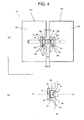
- FIG. 4 (a) and FIG. 4 (b) relate to the embodiment 2 of the present invention
- FIG. 4 (a) is a plan view of the wiring patterns 31A, 31B on which the chip component 41 is mounted as viewed from the top
- FIG. 4 (b) is an enlarged view of the region IVb of FIG. 4 (a) .
- the point of the wiring patterns 31A, 31B of the embodiment 2 different from the embodiment 1 is the point that the wiring portion 34a and the wiring portion 34b are extended in the y-direction from the lateral sides of the lands 33a, 33b, and connect the pattern portions 32a, 32b and the lands 33a, 33b to each other.
- the wiring pattern 31A and the wiring pattern 31B have the configurations described below.
- the distance from the center line Xo to the land x-direction outermost lateral side 51 that is outermost in the x-direction and the distance from the center line Xo to a wiring portion x-direction outermost lateral side 52 that is outermost in the x-direction are equal to each other.
- the land x-direction outermost lateral side 51 and the wiring portion x-direction outermost lateral side 52 are positioned on a same straight line.
- the embodiment 2 is similar to the embodiment 1, and the effect similar to that of the embodiment 1 is exerted in the embodiment 2 also.
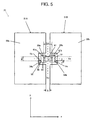
- FIG. 5 relates to the embodiment 3 of the present invention, and is a plan view of the wiring patterns 31A, 31B on which the chip component 41 is mounted as viewed from the top.
- the point of the wiring patterns 31A, 31B of the embodiment 3 different from the embodiment 2 is the point that the wiring portion 34a and the wiring portion 34b respectively have inclined portions.
- the wiring portions 34a, 34b respectively include a straight line portion and an inclined portion, the straight line portion is extended in the x-direction from the connection portion 56 with the lands 33a, 33b, and the inclined portion is arranged to continue to the straight line portion and connects the pattern portions 32a, 32b and the lands 33a, 33b to each other.
- the inclined portion is inclined in the direction of gradually departing from the lands 33a, 33b toward the pattern portions 32a, 32b.
- the land 33a and the land 33b as well as the wiring portion 34a and the wiring portion 34b are formed to be line-symmetric with each other respectively with respect to the center line Xo.
- the center Ya in the y-direction of the connection portion 56 is disposed outside of a region in which a region of the width Wc of the chip component 41 extends in the x-direction and a region in which a region of the length Lc of the chip component 41 extends in the y-direction.
- the connection portion 56 is connected to the land x-direction outermost lateral side 51 that is outermost in the x-direction of the lands 33a, 33b.
- the embodiment 3 also exerts the effect similar to that of the embodiments 1, 2.
- FIG. 6 relates to the embodiment 4 of the present invention, and is a plan view of the wiring patterns 31A, 31B on which the chip component 41 is mounted as viewed from the top.
- the point of the wiring patterns 31A, 31B of the embodiment 4 different from the embodiment 3 is the point that the inclined portion of the wiring portions 34a, 34b are inclined to the opposite direction to the inclined portion of the embodiment 3.
- the wiring portions 34a, 34b respectively include a straight line portion and an inclined portion, the straight line portion is extended in the x-direction from the connection portion 56 with the lands 33a, 33b, and the inclined portion is arranged to continue to the straight line portion and connects the pattern portions 32a, 32b and the lands 33a, 33b to each other similarly to the embodiment 2.
- the inclined portion is inclined to the direction of gradually approaching the center line Yo.
- the land 33a and the land 33b as well as the wiring portion 34a and the wiring portion 34b are formed to be line-symmetric with each other respectively with respect to the center line Xo.
- the center Ya in the y-direction of the connection portion 56 is disposed outside of a region in which a region of the width Wc of the chip component 41 extends in the x-direction and a region in which a region of the length Lc of the chip component 41 extends in the y-direction.
- the connection portion 56 is connected to the land x-direction outermost lateral side 51 that is outermost in the x-direction of the lands 33a, 33b.
- the embodiment 4 also exerts the effect similar to that of the embodiments 1-3.
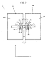
- FIG. 7 relates to the embodiment 5 of the present invention, and is a plan view of the wiring patterns 31A, 31B on which the chip component 41 is mounted as viewed from the top.
- the point of the wiring patterns 31A, 31B of the embodiment 5 different from the embodiment 3 shown in FIG. 5 is the point that the wiring portion 34a and the wiring portion 34b are inclined over the entire length.
- the land 33a and the land 33b as well as the wiring portion 34a and the wiring portion 34b are formed to be line-symmetric with each other respectively with respect to the center line Xo.
- the wiring portions 34a, 34b are extended respectively from the land connection portion 56 incliningly, and connect the pattern portions 32a, 32b and the lands 33a, 33b to each other.
- the wiring portions 34a, 34b are formed so as to incline from the connection portion 56 toward the pattern portions 32a, 32b to the direction of gradually departing from the center line Yo.
- connection portion 56 of the wiring portions 34a, 34b connected to the lands 33a, 33b is in a positional relation same to that of the embodiments 3, 4. More specifically, the center Ya in the y-direction of the connection portion 56 is disposed outside of a region in which a region of the width Wc of the chip component 41 extends in the x-direction and a region in which a region of the length Lc of the chip component 41 extends in the y-direction. Also, the connection portion 56 is connected to the portion outermost in the y-direction of the land x-direction outermost lateral side 51 that is outermost in the x-direction of the lands 33a, 33b.
- the embodiment 5 also exerts the effect similar to that of the embodiments 1-4.
- FIG. 8 relates to the embodiment 6 of the present invention, and is a plan view of the wiring patterns 31A, 31B on which the chip component 41 is mounted as viewed from the top.
- the point of the wiring patterns 31A, 31B of the embodiment 6 different from the embodiment 1 shown in FIG. 3 is the point that the wiring portions 34a, 34b are extended incliningly from the connection portion 53, and connect the pattern portions 32a, 32b and the lands 33a, 33b to each other.
- the wiring portions 34a, 34b are formed so as to incline from the connection portion 53 toward the pattern portions 32a, 32b to the direction of gradually approaching the center line Xo.
- the land 33a and the land 33b as well as the wiring portion 34a and the wiring portion 34b are formed to be line-symmetric with each other respectively with respect to the center line Xo.
- the center Xa in the x-direction of the connection portion 53 is disposed outside of a region in which a region of the width Wc of the chip component 41 extends in the x-direction and a region in which a region of the length Lc of the chip component 41 extends in the y-direction.
- the connection portion 53 is connected to the portion outermost in the x-direction of the land y-direction outermost lateral side 54 that is outermost in the y-direction of the lands 33a, 33b.
- the embodiment 6 also exerts the effect similar to that of the embodiments 1-5.
- FIG. 9 relates to the embodiment 7 of the present invention, and is a plan view of the wiring patterns 31A, 31B on which the chip component 41 is mounted as viewed from the top.
- the point of the wiring patterns 31A, 31B of the embodiment 7 different from the embodiment 4 shown in FIG. 6 is the point that the wiring portion 34a and the wiring portion 34b include not the inclined portion but a step-like routing portion.
- connection portion 56 of the wiring portions 34a, 34b connected to the lands 33a, 33b is in a positional relation same to that of the embodiment 4. More specifically, the center Ya in the y-direction of the connection portion 56 is disposed outside of a region in which a region of the width Wc of the chip component 41 extends in the x-direction and a region in which a region of the length Lc of the chip component 41 extends in the y-direction. Also, the connection portion 56 is connected to the land x-direction outermost lateral side 51 that is outermost in the x-direction of the lands 33a, 33b. Further, in the embodiment 7, the land 33a and the land 33b as well as the wiring portion 34a and the wiring portion 34b are formed to be line-symmetric with each other respectively with respect to the center line Xo.
- the embodiment 7 also exerts the effect similar to that of the embodiments 1-6.
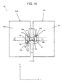
- FIG. 10 relates to the embodiment 8 of the present invention, and is a plan view of the wiring patterns 31A, 31B on which the chip component 41 is mounted as viewed from the top.
- the wiring portion 34a of the wiring pattern 31A and the wiring portion 34b of the wiring pattern 31B in the embodiment 8 are formed to be point-symmetric with each other with respect to the center O of the chip component 41.
- connection portion 53 of the wiring portion 34a connected to the land 33a and the connection portion 53 of the wiring portion 34b connected to the land 33b are disposed at the positions becoming symmetric with each other with respect to the center line Xo and the center line Yo.
- the centers Xa in the x-direction of the connection portions 53 are respectively disposed outside of a region in which a region of the width Wc of the chip component 41 extends in the x-direction and a region in which a region of the length Lc of the chip component 41 extends in the y-direction.
- the x-direction outermost lateral sides 52 which are the wiring portions of outermost in the x-direction of the wiring portions 34a, 34b are on the straight lines same to the land x-direction outermost lateral sides 51 which are outermost in the x-direction of the lands 33a, 33b respectively. Because the other configurations in the embodiment 8 are similar to those of the embodiment 2, explanation thereof will be omitted. Therefore, the embodiment 8 also exerts the effect similar to that of the embodiments 1-7.
- FIG. 11 relates to the embodiment 9 of the present invention, and is a plan view of the wiring patterns 31A, 31B on which the chip component 41 is mounted as viewed from the top.
- the wiring portion 34a of the wiring pattern 31A and the wiring portion 34b of the wiring pattern 31B are formed to be point-symmetric with each other with respect to the center O of the chip component 41.
- the wiring portions 34a, 34b are connected to the land x-direction outermost lateral sides 51 which are outermost in the x-direction of the lands 33a, 33b respectively.
- the wiring portions 34a, 34b respectively include the inclined portion and the straight line portion, the inclined portion is extended obliquely from the lands 33a, 33b, and the straight line portion arranged so as to continue to the end of the inclined portion in the x-direction is connected to the wiring patterns 31A, 31B.
- connection portion 56 of the wiring portions 34a, 34b connected to the lands 33a, 33b is in a positional relation same to that of the embodiment 4 shown in FIG. 6 . More specifically, the centers Ya in the y-direction of the connection portion 56 are respectively disposed outside of a region in which a region of the width Wc of the chip component 41 extends in the x-direction and a region in which a region of the length Lc of the chip component 41 extends in the y-direction. Also, the connection portion 56 is connected to the lateral side 51 that is outermost in the x-direction of the lands 33a, 33b.
- the embodiment 9 also exerts the effect similar to that of the embodiments 1-8.
- FIG. 12 relates to the embodiment 10 of the present invention, and is a plan view of the wiring patterns 31A, 31B on which the chip component 41 is mounted as viewed from the top.
- the embodiment 10 is different from the embodiment 9 in the point that the wiring portions 34a, 34b of the wiring patterns 31A, 31 B are formed of the incline portion only.
- the wiring portions 34a, 34b respectively include the inclined portion, and the pattern portions 32a, 32b and the lands 33a, 33b are connected to each other by this inclined portion.
- the wiring portion 34a and the wiring portion 34b are formed to be point-symmetric with each other with respect to the center O of the chip component 41.
- the center Ya in the y-direction of the connection portion 56 is disposed outside of a region in which a region of the width Wc of the chip component 41 extends in the x-direction and a region in which a region of the length Lc of the chip component 41 extends in the y-direction.
- the connection portion 56 is connected to the land x-direction outermost lateral side 51 that is outermost in the x-direction of the lands 33a, 33b.
- the embodiment 10 also exerts the effect similar to that of the embodiments 1-9.
- FIG. 13 relates to the embodiment 11 of the present invention, and is a plan view of the wiring patterns 31A, 31B on which the chip component 41 is mounted as viewed from the top.
- the embodiment 11 is same to the embodiment 10 in the point that the wiring portions 34a, 34b of the wiring patterns 31A, 31 B are formed of the inclined portion only, but is different from the embodiment 10 in the point that the wiring portions 34a, 34b are connected to the land y-direction outermost lateral side 54 that is outermost in the y-direction of the lands 33a, 33b.
- the wiring portions 34a, 34b respectively include the inclined portion, and the pattern portions 32a, 32b and the lands 33a, 33b are connected to each other by this inclined portion.
- the wiring portion 34a and the wiring portion 34b are formed to be point-symmetric with each other with respect to the center O of the chip component 41.
- the center Xa in the x-direction of the connection portion 53 is disposed outside of a region in which a region of the width Wc of the chip component 41 extends in the x-direction and a region in which a region of the length Lc of the chip component 41 extends in the y-direction.
- the connection portion 53 is connected to the portion outermost in the x-direction of the land y-direction outermost lateral side 54 that is outermost in the y-direction of the lands 33a, 33b.
- the embodiment 11 also exerts the effect similar to that of the embodiments 1-10.
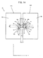
- FIG. 14 relates to the embodiment 12 of the present invention, and is a plan view of the wiring patterns 31A, 31B on which the chip component 41 is mounted as viewed from the top.
- the wiring portion 34a of the wiring pattern 31A and the wiring portion 34b of the wiring pattern 31B are disposed at the positions asymmetric with each other with respect to the center O of the chip component 41.
- the wiring portion 34a is connected to the land y-direction outermost lateral side 54 that is outermost in the y-direction of the land 33a at the connection portion 53.
- the wiring portion x-direction outermost lateral side 52 that is outermost in the x-direction of the wiring portion 34a is on the straight line same to the land x-direction outermost lateral side 51 that is outermost in the x-direction of the land 33a.
- the wiring portion 34b is connected to the land x-direction outermost lateral side 51 that is outermost in the x-direction of the land 33b at the connection portion 56.
- the land y-direction outermost lateral side 54 that is outermost in the y-direction of the land 33b is on the straight line same to the wiring portion y-direction outermost lateral side 55 that is outermost in the y-direction of the wiring portion 34b.
- the center Xa in the x-direction of the connection portion 53 of the wiring portion 34a and the center Ya in the y-direction of the connection portion 56 of the wiring portion 34b are respectively disposed outside of a region in which a region of the width Wc of the chip component 41 extends in the x-direction and a region in which a region of the length Lc of the chip component 41 extends in the y-direction.
- FIG. 15 relates to the embodiment 13 of the present invention, and is a plan view of the wiring patterns 31A, 31B on which the chip component 41 is mounted as viewed from the top.
- the wiring portion 34a of the wiring pattern 31A and the wiring portion 34b of the wiring pattern 31B are disposed at the positions asymmetric with each other with respect to the center O of the chip component 41, however, the embodiment 13 exhibits a form different from that of the embodiment 12.
- the wiring portion 34a is connected to the land y-direction outermost lateral side 54 that is outermost in the y-direction of the land 33a by the connection portion 53.
- the connection portion 53 of the embodiment 13 is arranged on the opposite side of that of the embodiment 12 with respect to the center line Yo.
- the wiring portion x-direction outermost lateral side 52 that is outermost in the x-direction of the wiring portion 34a is on the straight line same to the land x-direction outermost lateral side 51 that is outermost in the x-direction of the lands 33a, 33b.
- the wiring portion 34b is connected to the land x-direction outermost lateral side 51 that is outermost in the x-direction of the land 33b by the connection portion 53. Also, the wiring portion 34b includes a straight line portion and an inclined portion, the straight line portion is extended in the y-direction from the land 33b, and the inclined portion is arranged to continue to the end of the straight line portion and is connected to the pattern portion 32b. As described above, the shape of the drawing out portion extended out from the connection portion 56 toward the pattern portion 32b does not affect the action of the crack generated in the connection portion of the solder 42.
- FIG. 16 relates to the embodiment 14 of the present invention, and is a plan view of the wiring patterns 31A, 31B on which the chip component 41 is mounted as viewed from the top.
- the wiring portion 34a of the wiring pattern 31A and the wiring portion 34b of the wiring pattern 31B are disposed at the positions asymmetric with each other with respect to the center O of the chip component 41, however, the embodiment 14 exhibits a form different from that of the embodiments 12, 13.
- the embodiment 14 is same to the embodiment 13 in the point that the wiring portion 34b of the wiring pattern 31B includes an inclined portion, but is different from the embodiment 13 only in the point that the inclination direction of the inclined portion is opposite.
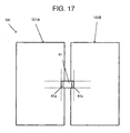
- FIG. 17 is a plan view of the comparative example 1 of wiring patterns 131A, 131B on which the chip component 41 is mounted as viewed from the top.
- the wiring patterns 131 A, 131B are solid patterns, and do not include a land and a wiring portion.
- the electrodes 41a, 41b of the chip component 41 were soldered directly to the wiring patterns 131A, 131B.
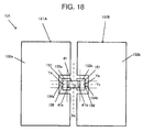
- FIG. 18 is a plan view of the comparative example 2 of the wiring patterns 131 A, 131B on which the chip component 41 is mounted as viewed from the top.
- the wiring patterns 131A, 131B include pattern portions 132a, 132b, lands 133a, 133b, and wiring portions 134a, 134b.
- connection portions 156 are disposed within a region in which a region of the width Wc of the chip component 41 extends in the x-direction. Therefore, naturally, the center Ya in the y-direction of the connection portion 156 is disposed within a range in which a region of the width Wc of the chip component 41 extends in the x-direction.
- the test condition is as follows.
- the circuit wiring board 30 For the circuit wiring board 30, one with the base board 38 of an aluminum material with 50 mm square and 2 mm thickness was used.
- the insulation layer 37 was arranged on the base board 38, and the wiring patterns 31A, 31B or 131A, 131B were formed on the insulation layer 37 by a copper foil.
- a chip resistor of 1608 (1.6 mm ⁇ 0.8 mm) size was used.
- the electrodes 41a, 42b of the chip component 41 were soldered to the wiring patterns 31A, 31B or 131A, 131B using a lead-free solder of Sn3Ag0.5Cu.
- the temperature cycle test of -30/80°C was executed.
- the resistance value of each sample was measured at every 500 cycles, and the case with 10% or more of the resistance value variation was determined to be the wire breakage.
- the wire breakage occurred in 3 samples at 1,500 cycles, and in all 5 samples at 2,000 cycles or more.
- the wire breakage occurred in 2 samples at 1,500 cycles, and in all 5 samples at 2,000 cycles or more.
- the embodiment 2 and the embodiment 8 of the present invention it was confirmed that the wire breakage did not occur even after executing 3,000 cycles. By this test, the effect by the present invention was endorsed.
- the wiring patterns 31A, 31B shown in the embodiments 1-15 described above are examples of the preferred aspect, and the shape, size and the like of the pattern portions 32a, 32b, the lands 33a, 33b, and the wiring portions 34a, 34b can be modified appropriately.
- the lands 33a, 33b are not limited to the rectangular shape, and may be of other polygons and the shape having a curved line portion such as an arc section or a hypotenuse portion in the outline.
- the pattern portion 32a and the pattern portion 32b may be of an asymmetric shape with each other, and may be of different shapes.
- the wiring route of the wiring portions 34a, 34b is free, and an arc portion and a curved line portion may be included.
- the material for connection is not limited to the solder 42, but can be applied to the laser welding, resistance welding, and the like in which one of the land or the electrode is molten for joining.
- the chip component 41 is not limited to the rectangular shape in a plan view, and may have a profile including an arc portion and a curved line portion.
- the electronic control device of the present invention only has to be one in which the center in the width direction in the connection portion of the wiring portion connected to the land is disposed outside of both of a region in which a region of the width of the electronic component extends in the longitudinal direction of the electronic component and a region in which a region of the length of the electronic component extends in the transverse direction of the electronic component.
Landscapes
- Engineering & Computer Science (AREA)
- Microelectronics & Electronic Packaging (AREA)
- Manufacturing & Machinery (AREA)
- Electric Connection Of Electric Components To Printed Circuits (AREA)
- Semiconductor Integrated Circuits (AREA)
Abstract
Description
- The present invention relates to an electronic control device including a circuit wiring board in which an electronic component is connected to a land.
- On a vehicle such as an automobile, various electronic control devices for engine control, for motor control, for automatic transmission control, and the like for example are mounted. As the electronic control device, there is one including a MOSFET for switching an inverter device, a DC-DC converter device, and the like, a capacitor module, and the like. Such electronic control device includes a circuit wiring board having plural solid wiring patterns and a chip component in which the electrodes formed in both ends are soldered to the wiring patterns.
- Because an electronic control device for a vehicle is installed under an environment with sharp temperature change, solid wiring patterns and a chip component repeat expansion and shrinkage, and a crack is liable to occur in solder that connects the chip component and the wiring patterns to each other.
- As a countermeasure for it, a surface mounting structure is known in which lands soldered to the electrodes of the chip component and wiring that connects the lands and the wiring patterns to each other are arranged in a circuit wiring board. With the surface mounting structure, it is assumed that the stress applied to the solder can be absorbed by making the width of the wiring narrower than the width of the chip component soldered to the land. The connection part of each land and the wiring is disposed within a region in which the region of the width of the chip component extends in the longitudinal direction or within a region in which the region of the length of the chip component extends in the transverse direction (refer to
FIG. 1(a) ofPatent Literature 1 for example). - Patent Literature 1:
JP-A-2008-72065 - In the electronic control device described in
Patent Literature 1, the connection portion of each land and the wiring is disposed within a region in which the region of the width of the chip component extends in the longitudinal direction or within a region in which the region of the length of the chip component extends in the transverse direction. In this structure, the distances from the wiring to the solder connection portions connected to both side surfaces of the chip component are generally equal to each other. Therefore, a large stress is generated in both sides in the width direction of the solder connection portion formed on the land, and the crack is liable to occur in both sides in the width direction of this solder connection portion formed on the land. Although the crack generated in the solder connection portion progresses from both sides in the width direction of the solder connection portion toward the center, because the distance to the position where the crack reaches the center in the width direction of the connection portion and wire breakage occurs is short, the lifetime becomes short which lacks the reliability. - An electronic control device of the present invention includes a circuit wiring board in which a wiring pattern is formed on a base metal, with the wiring pattern including a pair of patterns having a large area, a pair of lands arranged between the pair of patterns at a predetermined interval and having an area smaller than that of the pattern, and a pair of wiring portions connecting the pair of lands and the pair of patterns respectively, and an electronic component in which electrodes having a predetermined length and a predetermined width and arranged in one end and the other end in the longitudinal direction respectively are connected to the respective lands respectively, in which the wiring portions are arranged so that the center in the width direction of the connection portion connected to the land is disposed at a position that is outside of both a region in which a region of the predetermined width of the electronic component extends in the longitudinal direction of the electronic component and a region in which a region of the predetermined length of the electronic component extends in the transverse direction of the electronic component.
- According to the present invention, because the length to the point where the wire breakage caused by the crack of the solder occurs becomes long, the lifetime until the wire breakage can be made long, and the reliability can be improved.
-
- [
FIG. 1] FIG. 1 is a cross-sectional view of an electronic control device according to the present invention. - [
FIG. 2] FIG. 2 is an enlarged cross-sectional view of a circuit wiring board illustrated inFIG. 1 on which the chip component is mounted. - [
FIG. 3 ] (a) is a plan view of a wiring pattern illustrated inFIG. 2 on which the chip component is mounted as viewed from the top, and (b) is an enlarged view of the region IIIb of (a). - [
FIG. 4] FIG. 4 relates to theembodiment 2 of the present invention, (a) is a plan view ofwiring patterns chip component 41 is mounted as viewed from the top, and (b) is an enlarged view of the region IVb of (a). - [
FIG. 5] FIG. 5 relates to theembodiment 3 of the present invention, and is a plan view of a wiring pattern on which a chip component is mounted as viewed from the top. - [
FIG. 6] FIG. 6 relates to the embodiment 4 of the present invention, and is a plan view of a wiring pattern on which a chip component is mounted as viewed from the top. - [
FIG. 7] FIG. 7 relates to theembodiment 5 of the present invention, and is a plan view of a wiring pattern on which a chip component is mounted as viewed from the top. - [
FIG. 8] FIG. 8 relates to theembodiment 6 of the present invention, and is a plan view of a wiring pattern on which a chip component is mounted as viewed from the top. - [
FIG. 9] FIG. 9 relates to the embodiment 7 of the present invention, and is a plan view of a wiring pattern on which a chip component is mounted as viewed from the top. - [
FIG. 10] FIG. 10 relates to the embodiment 8 of the present invention, and is a plan view of a wiring pattern on which a chip component is mounted as viewed from the top. - [
FIG. 11] FIG. 11 relates to the embodiment 9 of the present invention, and is a plan view of a wiring pattern on which a chip component is mounted as viewed from the top. - [
FIG. 12] FIG. 12 relates to theembodiment 10 of the present invention, and is a plan view of a wiring pattern on which a chip component is mounted as viewed from the top. - [
FIG. 13] FIG. 13 relates to the embodiment 11 of the present invention, and is a plan view of a wiring pattern on which a chip component is mounted as viewed from the top. - [
FIG. 14] FIG. 14 relates to the embodiment 12 of the present invention, and is a plan view of a wiring pattern on which a chip component is mounted as viewed from the top. - [
FIG. 15] FIG. 15 relates to the embodiment 13 of the present invention, and is a plan view of a wiring pattern on which a chip component is mounted as viewed from the top. - [
FIG. 16] FIG. 16 relates to the embodiment 14 of the present invention, and is a plan view of a wiring pattern on which a chip component is mounted as viewed from the top. - [
FIG. 17] FIG. 17 is a plan view of a wiring pattern on which a chip component is mounted as viewed from the top shown as the comparative example 1. - [
FIG. 18] FIG. 18 is a plan view of a wiring pattern on which a chip component is mounted as viewed from the top shown as the comparative example 2. - [
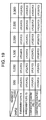
FIG. 19] FIG. 19 is a drawing showing a test result of the wire breakage by the crack generated in the solder connection portion. - Below, an embodiment of an electronic control device related to the present invention will be explained referring to the drawings.
-
FIG. 1 is a cross-sectional view of anelectronic control device 10, andFIG. 2 is an enlarged cross-sectional view of a circuit wiring board illustrated inFIG. 1 on which a chip component is mounted. - The
electronic control device 10 illustrated inFIG. 1 is used for engine control, motor control, automatic transmission control, and the like of a vehicle such as an automobile for example. - The
electronic control device 10 includes acase 3 formed of acase base portion 1 and acase cover portion 2 that seals thecase base portion 1. Inside thecase 3, acircuit wire board 30, a chip component (electronic component) 41 mounted on thecircuit wire board 30, acapacitor module 6, a circuit board for control 4, and aconductor 5 such as a bus bar are stored. - The
case base portion 1 and thecase cover portion 2 are formed of a metal having a main composition of aluminum, iron and copper, a ceramic, or a resin such as a glass epoxy resin, are fixed by a fastening member and the like not illustrated through a seal member not illustrated, and construct a sealing structure. - Although it is not illustrated, the
capacitor module 6 is formed by storing X-capacitors imposed between the phases and Y-capacitors imposed between each phase and a chassis within a capacitor case, and flattens the noise inputted to the circuit board for control 4. - One
electrode 6a of thecapacitor module 6 is connected to the circuit board for control 4, and theother electrode 6b is connected to thecircuit wiring board 30. The circuit board for control 4 and thecircuit wiring board 30 are connected to each other by theconductor 5. - The
circuit wiring board 30 includes abase board 38 formed of a metal having the main composition of aluminum, iron and copper or a resin, aninsulation layer 37 formed on one surface of thebase board 38, andplural wiring patterns 31 formed on theinsulation layer 37. - The
chip component 41 is a passive element such as a capacitor and a resistor, and includes a pair ofelectrodes electrodes lands FIG. 3 ) of thewiring patterns 31 respectively, and are soldered bysolder 42. Thesolder 42 is formed of a material not containing lead (lead-free) such as SnAgCu for example. -
FIG. 3 (a) is a plan view of thewiring pattern 31 illustrated inFIG. 2 on which thechip component 41 is mounted as viewed from the top, andFIG. 3 (b) is an enlarged view of the region IIIb ofFIG. 3 (a) . - Also, on the
insulation layer 37, a number of wiring patterns are formed to which an active component such as a MOSFET for switching and a number of chip components are connected, however, below, onechip component 41 and a pair ofwiring patterns - In
FIGs. 3 (a), 3(b) , the reference sign Xo is a straight line extending in the y-direction and passing through the center O of thechip component 41, and is referred to as the center line Xo in the present description. Also, the reference sign Yo is a straight line extending in the x-direction and passing through the center O of thechip component 41, and is referred to as the center line Yo in the present description. Also, inFIGs. 3 (a), 3(b) , the y-direction is the transverse direction of thechip component 41, and is referred to also as the chip transverse direction. The x-direction is the longitudinal direction of thechip component 41, and is referred to also as the chip longitudinal direction. - The
wiring pattern 31A includes apattern portion 32a, theland 33a, and awiring portion 34a that connects thepattern portion 32a and theland 33a to each other. Thepattern portion 32a has a large area, and is wound around into a predetermined shape on thebase board 38. Similarly, thewiring pattern 31B includes apattern portion 32b, theland 33b, and awiring portion 34b that connects thepattern portion 32b and theland 33b to each other. Thepattern portion 32b has a large area, and is wound around into a predetermined shape on thebase board 38. - The
chip component 41 has a predetermined length Lc in the x-direction (the chip component longitudinal direction) and a predetermined width Wc in the y-direction (the chip component transverse direction), and has a rectangular shape in the plan view in which the length Lc is larger than the width Wc. The width Wc of thechip component 41 is smaller than the length in the y-direction of thelands - The
land 33a and theland 33b are disposed so as to be apart from each other by the interval S in the x-direction, and theelectrodes chip component 41 are placed on thelands solder 42. InFIGs. 3 (a), 3(b) , illustration of thesolder 42 is omitted to make the drawing clear. - The
lands lands wiring patterns - The
wiring portion 34a and thewiring portion 34b are formed into a same shape and a same size, and the width Wa that is the length in the y-direction is made shorter than the length in the y-direction of theland 33a respectively. The width Wa of thewiring portions wiring portions reference sign 55, and is referred to as a wiring portion y-direction outermost lateral side. Also, the lateral side that is outermost in the y-direction of thelands reference sign 54, and is referred to as a land y-direction outermost lateral side. - With respect to the
chip component 41, the center O thereof is disposed generally on the center line of the interval S between the lands. Theland 33a and theland 33b as well as thewiring portion 34a and thewiring portion 34b are disposed to be line-symmetric with each other respectively with respect to the center line Yo. - The
wiring portion 34a and thewiring portion 34b are extended from theland 33a and theland 33b so as to be generally perpendicular to the y-direction, or, in other words, in parallel with the x-direction, and connect thepattern portions lands wiring portions lateral sides 51 of thelands connection portions 56. The distance from the center line Yo to the land y-direction outermostlateral side 54 and the distance from the center line Yo to the wiring portion y-direction outermostlateral side 55 are equal to each other. In other words, the land y-direction outermostlateral side 54 and the wiring portion y-direction outermostlateral side 55 are arrayed on one straight line. - As illustrated in
FIG. 3 (b) , the center Ya in the y-direction in a line segment 56 (hereinafter referred to also as the connection portion 56) that is the connection portion where thelands wiring portions chip component 41 extends in the x-direction (the chip component longitudinal direction). The center Ya in the y-direction in theconnection portion 56 described above is disposed outside of a region in which a region of the length Lc of thechip component 41 extends in the y-direction (the chip component transverse direction). - More specifically, the
wiring pattern 31A and thewiring pattern 31B have the configurations described below. - (a) The distance from the center line Yo that extends in the chip component longitudinal direction to the land y-direction outermost
lateral side 54 and the distance from the center line Yo to the wiring portion y-direction outermostlateral side 55 are equal to each other. Also, theland 33a and theland 33b as well as thewiring portion 34a and thewiring portion 34b are disposed to be line-symmetric with each other respectively with respect to the center line Xo that extends in the chip component transverse direction. - (b) The
wiring portions pattern portions lands - (c) The center Ya in the y-direction of the
line segment 56 that is the connection portion of thelands wiring portions chip component 41 extends in the x-direction (the chip component longitudinal direction). Also, the center Ya in the y-direction of theconnection portion 56 is disposed outside of a region in which a region of the length Lc of thechip component 41 extends in the y-direction (the chip component transverse direction). - According to the
electronic control device 10 of an embodiment described above, the actions and effects described below are exerted. - (1) The
wiring patterns base board 38 through theinsulation layer 37. Thewiring patterns pattern portions lands pattern portions wiring portions lands pattern portions lands
Here, "thelands pattern portions lands wiring portions lands wiring patterns
By employing such pattern structure, when thebase board 38 and thewiring patterns insulation layer 37 also deforms by thermal expansion and thermal shrinkage. By this deformation of theinsulation layer 37, the stress generated in the solder connection portion can be suppressed. In addition, in thewiring portions lands solder 42 by a thermal stress can be suppressed. - (2) As described in the configuration (c), the center Ya in the y-direction of the
line segment 56 that is the connection portion of thelands wiring portions chip component 41 extends in the x-direction, and is disposed outside of a region in which a region of the length Lc of thechip component 41 extends in the y-direction.
According to the prior art, the center Ya in the y-direction of theconnection portion 56 is disposed within a region in which a region of the width Wc of thechip component 41 extends in the x-direction (the chip component longitudinal direction). In other words, the distances from the wiring portion to the solder connection portions connected to both side surfaces of thechip component 41 are generally equal to each other. Therefore, a large stress is generated in both sides in the width direction of the solder connection portion formed on the land, and the crack is liable to occur in both sides in the width direction of this solder connection portion formed on the land. Although the crack generated in the solder connection portion progresses from both sides in the width direction of the solder connection portion toward the center, because the distance to the position where the crack reaches the center in the width direction of the connection portion and wire breakage occurs is short, the lifetime becomes short which lacks the reliability.
On the other hand, according to an embodiment described above, the center Ya in the width direction of the respective connection portions of thewiring portions lands pattern portions chip component 41 extends in the longitudinal direction of thechip component 41 and a region in which a region of the length Lc of thechip component 41 extends in the transverse direction of thechip component 41. The stress generated in the solder connection portion of both side surfaces in the y-direction of thechip component 41 becomes larger as the distance from thewiring portions wiring portions wiring portions solder 42 is liable to be generated in the solder connection portion on the side nearer from thewiring portions wiring portions wiring portions solder 42 occurs becomes long. In other words, the life time until the wire breakage can be made long, and the reliability can be improved.
Also, according to an example of a prior art, because similar cracks are generated in the solder connection portions in both ends in the y-direction and mutually develop, the distance to the position where wire breakage occurs becomes a half of the distance between the solder connection portions in both ends in the y-direction. - (3) In addition to the configuration (c) described above, as described in the configuration (b) described above, the distance to the land y-direction outermost
lateral side 54 of thelands lateral side 55 of thewiring portions lateral side 55 of thewiring portions chip component 41 in thelands wiring portions chip component 41 thus, the stress generated in the solder connection portion can be reduced. - Also, with respect to the
wiring patterns -
FIG. 4 (a) and FIG. 4 (b) relate to theembodiment 2 of the present invention,FIG. 4 (a) is a plan view of thewiring patterns chip component 41 is mounted as viewed from the top, andFIG. 4 (b) is an enlarged view of the region IVb ofFIG. 4 (a) . - The point of the
wiring patterns embodiment 2 different from theembodiment 1 is the point that thewiring portion 34a and thewiring portion 34b are extended in the y-direction from the lateral sides of thelands pattern portions lands - More specifically, the
wiring pattern 31A and thewiring pattern 31B have the configurations described below. - (a) The
land 33a and theland 33b as well as thewiring portion 34a and thewiring portion 34b are formed to be line-symmetric with each other respectively with respect to the center line Xo. - (b) The
wiring portions pattern portions lands wiring portions lands connection portions 53. Theland lateral side 54 is positioned outermost in the x-direction from the center line Xo out of 4 sides which are the contour lines of thelands - (c) The center Xa in the x-direction of a line segment 53 (hereinafter referred to also as the connection portion 53) which is the connection portion of the
lands wiring portions chip component 41 extends in the y-direction. Also, the center Xa in the x-direction of theconnection portion 53 is disposed outside of a region in which a region of the width Wc of thechip component 41 extends in the x-direction. - Also, in the
embodiment 2, the distance from the center line Xo to the land x-direction outermostlateral side 51 that is outermost in the x-direction and the distance from the center line Xo to a wiring portion x-direction outermostlateral side 52 that is outermost in the x-direction are equal to each other. In other words, the land x-direction outermostlateral side 51 and the wiring portion x-direction outermostlateral side 52 are positioned on a same straight line. - Because the other configurations in the
embodiment 2 are similar to those of theembodiment 1, explanation thereof will be omitted. - With respect to the crack of the
solder 42, theembodiment 2 is similar to theembodiment 1, and the effect similar to that of theembodiment 1 is exerted in theembodiment 2 also. -
FIG. 5 relates to theembodiment 3 of the present invention, and is a plan view of thewiring patterns chip component 41 is mounted as viewed from the top. - The point of the
wiring patterns embodiment 3 different from theembodiment 2 is the point that thewiring portion 34a and thewiring portion 34b respectively have inclined portions. - The
wiring portions connection portion 56 with thelands pattern portions lands lands pattern portions - Because the other configurations in the
embodiment 3 are similar to those of theembodiment 2, explanation thereof will be omitted. - In the
embodiment 3, theland 33a and theland 33b as well as thewiring portion 34a and thewiring portion 34b are formed to be line-symmetric with each other respectively with respect to the center line Xo. Also, in theembodiment 3, the center Ya in the y-direction of theconnection portion 56 is disposed outside of a region in which a region of the width Wc of thechip component 41 extends in the x-direction and a region in which a region of the length Lc of thechip component 41 extends in the y-direction. Also, theconnection portion 56 is connected to the land x-direction outermostlateral side 51 that is outermost in the x-direction of thelands - Therefore, the
embodiment 3 also exerts the effect similar to that of theembodiments -
FIG. 6 relates to the embodiment 4 of the present invention, and is a plan view of thewiring patterns chip component 41 is mounted as viewed from the top. - The point of the
wiring patterns embodiment 3 is the point that the inclined portion of thewiring portions embodiment 3. - The
wiring portions connection portion 56 with thelands pattern portions lands embodiment 2. The inclined portion is inclined to the direction of gradually approaching the center line Yo. - Because the other configurations in the embodiment 4 are similar to those of the
embodiment 3, explanation thereof will be omitted. - In the embodiment 4, the
land 33a and theland 33b as well as thewiring portion 34a and thewiring portion 34b are formed to be line-symmetric with each other respectively with respect to the center line Xo. Also, in the embodiment 4, the center Ya in the y-direction of theconnection portion 56 is disposed outside of a region in which a region of the width Wc of thechip component 41 extends in the x-direction and a region in which a region of the length Lc of thechip component 41 extends in the y-direction. Also, theconnection portion 56 is connected to the land x-direction outermostlateral side 51 that is outermost in the x-direction of thelands - Therefore, the embodiment 4 also exerts the effect similar to that of the embodiments 1-3.
-
FIG. 7 relates to theembodiment 5 of the present invention, and is a plan view of thewiring patterns chip component 41 is mounted as viewed from the top. - The point of the
wiring patterns embodiment 5 different from theembodiment 3 shown inFIG. 5 is the point that thewiring portion 34a and thewiring portion 34b are inclined over the entire length. - In the
embodiment 5 also, theland 33a and theland 33b as well as thewiring portion 34a and thewiring portion 34b are formed to be line-symmetric with each other respectively with respect to the center line Xo. - The
wiring portions land connection portion 56 incliningly, and connect thepattern portions lands - The
wiring portions connection portion 56 toward thepattern portions - In the
embodiment 5 also, theconnection portion 56 of thewiring portions lands embodiments 3, 4. More specifically, the center Ya in the y-direction of theconnection portion 56 is disposed outside of a region in which a region of the width Wc of thechip component 41 extends in the x-direction and a region in which a region of the length Lc of thechip component 41 extends in the y-direction. Also, theconnection portion 56 is connected to the portion outermost in the y-direction of the land x-direction outermostlateral side 51 that is outermost in the x-direction of thelands - Because the other configurations in the
embodiment 5 are similar to those of theembodiments 3, 4, explanation thereof will be omitted. Therefore, theembodiment 5 also exerts the effect similar to that of the embodiments 1-4. -
FIG. 8 relates to theembodiment 6 of the present invention, and is a plan view of thewiring patterns chip component 41 is mounted as viewed from the top. - The point of the
wiring patterns embodiment 6 different from theembodiment 1 shown inFIG. 3 is the point that thewiring portions connection portion 53, and connect thepattern portions lands - The
wiring portions connection portion 53 toward thepattern portions - The
land 33a and theland 33b as well as thewiring portion 34a and thewiring portion 34b are formed to be line-symmetric with each other respectively with respect to the center line Xo. - In the
embodiment 6, the center Xa in the x-direction of theconnection portion 53 is disposed outside of a region in which a region of the width Wc of thechip component 41 extends in the x-direction and a region in which a region of the length Lc of thechip component 41 extends in the y-direction. Also, theconnection portion 53 is connected to the portion outermost in the x-direction of the land y-direction outermostlateral side 54 that is outermost in the y-direction of thelands - Because the other configurations in the
embodiment 6 are similar to those of theembodiment 1, explanation thereof will be omitted. Therefore, theembodiment 6 also exerts the effect similar to that of the embodiments 1-5. -
FIG. 9 relates to the embodiment 7 of the present invention, and is a plan view of thewiring patterns chip component 41 is mounted as viewed from the top. - The point of the
wiring patterns FIG. 6 is the point that thewiring portion 34a and thewiring portion 34b include not the inclined portion but a step-like routing portion. - However, in the embodiment 7, the
connection portion 56 of thewiring portions lands connection portion 56 is disposed outside of a region in which a region of the width Wc of thechip component 41 extends in the x-direction and a region in which a region of the length Lc of thechip component 41 extends in the y-direction. Also, theconnection portion 56 is connected to the land x-direction outermostlateral side 51 that is outermost in the x-direction of thelands land 33a and theland 33b as well as thewiring portion 34a and thewiring portion 34b are formed to be line-symmetric with each other respectively with respect to the center line Xo. - Because the other configurations in the embodiment 7 are similar to those of the
embodiment 2, explanation thereof will be omitted. - Therefore, the embodiment 7 also exerts the effect similar to that of the embodiments 1-6.
-
FIG. 10 relates to the embodiment 8 of the present invention, and is a plan view of thewiring patterns chip component 41 is mounted as viewed from the top. - Differently from the embodiments 1-7, the
wiring portion 34a of thewiring pattern 31A and thewiring portion 34b of thewiring pattern 31B in the embodiment 8 are formed to be point-symmetric with each other with respect to the center O of thechip component 41. - The
connection portion 53 of thewiring portion 34a connected to theland 33a and theconnection portion 53 of thewiring portion 34b connected to theland 33b are disposed at the positions becoming symmetric with each other with respect to the center line Xo and the center line Yo. However, the centers Xa in the x-direction of theconnection portions 53 are respectively disposed outside of a region in which a region of the width Wc of thechip component 41 extends in the x-direction and a region in which a region of the length Lc of thechip component 41 extends in the y-direction. Also, the x-direction outermostlateral sides 52 which are the wiring portions of outermost in the x-direction of thewiring portions lateral sides 51 which are outermost in the x-direction of thelands embodiment 2, explanation thereof will be omitted. Therefore, the embodiment 8 also exerts the effect similar to that of the embodiments 1-7. -
FIG. 11 relates to the embodiment 9 of the present invention, and is a plan view of thewiring patterns chip component 41 is mounted as viewed from the top. - In the embodiment 9 also, the
wiring portion 34a of thewiring pattern 31A and thewiring portion 34b of thewiring pattern 31B are formed to be point-symmetric with each other with respect to the center O of thechip component 41. - The
wiring portions lateral sides 51 which are outermost in the x-direction of thelands wiring portions lands wiring patterns - In the embodiment 9, the
connection portion 56 of thewiring portions lands FIG. 6 . More specifically, the centers Ya in the y-direction of theconnection portion 56 are respectively disposed outside of a region in which a region of the width Wc of thechip component 41 extends in the x-direction and a region in which a region of the length Lc of thechip component 41 extends in the y-direction. Also, theconnection portion 56 is connected to thelateral side 51 that is outermost in the x-direction of thelands - Because the other configurations in the embodiment 9 are similar to those of the embodiment 4, explanation thereof will be omitted. Therefore, the embodiment 9 also exerts the effect similar to that of the embodiments 1-8.
-
FIG. 12 relates to theembodiment 10 of the present invention, and is a plan view of thewiring patterns chip component 41 is mounted as viewed from the top. - The
embodiment 10 is different from the embodiment 9 in the point that thewiring portions wiring patterns - The
wiring portions pattern portions lands wiring portion 34a and thewiring portion 34b are formed to be point-symmetric with each other with respect to the center O of thechip component 41. - In the
embodiment 10 also, the center Ya in the y-direction of theconnection portion 56 is disposed outside of a region in which a region of the width Wc of thechip component 41 extends in the x-direction and a region in which a region of the length Lc of thechip component 41 extends in the y-direction. Also, theconnection portion 56 is connected to the land x-direction outermostlateral side 51 that is outermost in the x-direction of thelands - Because the other configurations in the
embodiment 10 are similar to those of the embodiment 4, explanation thereof will be omitted. Therefore, theembodiment 10 also exerts the effect similar to that of the embodiments 1-9. -
FIG. 13 relates to the embodiment 11 of the present invention, and is a plan view of thewiring patterns chip component 41 is mounted as viewed from the top. - The embodiment 11 is same to the
embodiment 10 in the point that thewiring portions wiring patterns embodiment 10 in the point that thewiring portions lateral side 54 that is outermost in the y-direction of thelands - In the embodiment 11, the
wiring portions pattern portions lands wiring portion 34a and thewiring portion 34b are formed to be point-symmetric with each other with respect to the center O of thechip component 41. - In the embodiment 11 also, the center Xa in the x-direction of the
connection portion 53 is disposed outside of a region in which a region of the width Wc of thechip component 41 extends in the x-direction and a region in which a region of the length Lc of thechip component 41 extends in the y-direction. Also, theconnection portion 53 is connected to the portion outermost in the x-direction of the land y-direction outermostlateral side 54 that is outermost in the y-direction of thelands - Because the other configurations in the embodiment 11 are similar to those of the
embodiment 1, explanation thereof will be omitted. Therefore, the embodiment 11 also exerts the effect similar to that of the embodiments 1-10. -
FIG. 14 relates to the embodiment 12 of the present invention, and is a plan view of thewiring patterns chip component 41 is mounted as viewed from the top. - In the embodiment 12, the
wiring portion 34a of thewiring pattern 31A and thewiring portion 34b of thewiring pattern 31B are disposed at the positions asymmetric with each other with respect to the center O of thechip component 41. - In the embodiment 12, the
wiring portion 34a is connected to the land y-direction outermostlateral side 54 that is outermost in the y-direction of theland 33a at theconnection portion 53. The wiring portion x-direction outermostlateral side 52 that is outermost in the x-direction of thewiring portion 34a is on the straight line same to the land x-direction outermostlateral side 51 that is outermost in the x-direction of theland 33a. - The
wiring portion 34b is connected to the land x-direction outermostlateral side 51 that is outermost in the x-direction of theland 33b at theconnection portion 56. The land y-direction outermostlateral side 54 that is outermost in the y-direction of theland 33b is on the straight line same to the wiring portion y-direction outermostlateral side 55 that is outermost in the y-direction of thewiring portion 34b. - The center Xa in the x-direction of the
connection portion 53 of thewiring portion 34a and the center Ya in the y-direction of theconnection portion 56 of thewiring portion 34b are respectively disposed outside of a region in which a region of the width Wc of thechip component 41 extends in the x-direction and a region in which a region of the length Lc of thechip component 41 extends in the y-direction. - The other configurations of the embodiment 12 are similar to those of the
embodiment 1. - Therefore, in the embodiment 12 also, the effect similar to that of the embodiments 1-11 is exerted.
-
FIG. 15 relates to the embodiment 13 of the present invention, and is a plan view of thewiring patterns chip component 41 is mounted as viewed from the top. - In the embodiment 13, the
wiring portion 34a of thewiring pattern 31A and thewiring portion 34b of thewiring pattern 31B are disposed at the positions asymmetric with each other with respect to the center O of thechip component 41, however, the embodiment 13 exhibits a form different from that of the embodiment 12. - In the embodiment 13, the
wiring portion 34a is connected to the land y-direction outermostlateral side 54 that is outermost in the y-direction of theland 33a by theconnection portion 53. Theconnection portion 53 of the embodiment 13 is arranged on the opposite side of that of the embodiment 12 with respect to the center line Yo. The wiring portion x-direction outermostlateral side 52 that is outermost in the x-direction of thewiring portion 34a is on the straight line same to the land x-direction outermostlateral side 51 that is outermost in the x-direction of thelands - The
wiring portion 34b is connected to the land x-direction outermostlateral side 51 that is outermost in the x-direction of theland 33b by theconnection portion 53. Also, thewiring portion 34b includes a straight line portion and an inclined portion, the straight line portion is extended in the y-direction from theland 33b, and the inclined portion is arranged to continue to the end of the straight line portion and is connected to thepattern portion 32b. As described above, the shape of the drawing out portion extended out from theconnection portion 56 toward thepattern portion 32b does not affect the action of the crack generated in the connection portion of thesolder 42. - The other configurations in the embodiment 13 are similar to those of the
embodiment 1. Therefore, in the embodiment 13 also, the effect similar to that of the embodiments 1-12 is exerted. -
FIG. 16 relates to the embodiment 14 of the present invention, and is a plan view of thewiring patterns chip component 41 is mounted as viewed from the top. - In the embodiment 14 also, the
wiring portion 34a of thewiring pattern 31A and thewiring portion 34b of thewiring pattern 31B are disposed at the positions asymmetric with each other with respect to the center O of thechip component 41, however, the embodiment 14 exhibits a form different from that of the embodiments 12, 13. - The embodiment 14 is same to the embodiment 13 in the point that the
wiring portion 34b of thewiring pattern 31B includes an inclined portion, but is different from the embodiment 13 only in the point that the inclination direction of the inclined portion is opposite. - However, all of the other configurations are same to those of the embodiment 13.
- Therefore, in the embodiment 14 also, the effect similar to that of the embodiments 1-13 is exerted.
- The wire breakage caused by the crack in the solder connection portion of the
electrodes lands chip component 41 was evaluated by the test. - In the test, the
embodiment 2, the embodiment 8, the comparative example 1 and the comparative example 2 were compared. -
FIG. 17 is a plan view of the comparative example 1 ofwiring patterns chip component 41 is mounted as viewed from the top. - The
wiring patterns electrodes chip component 41 were soldered directly to thewiring patterns -
FIG. 18 is a plan view of the comparative example 2 of thewiring patterns chip component 41 is mounted as viewed from the top. - The
wiring patterns pattern portions lands wiring portions - The
wiring portions lateral sides 151 which are outermost in the x-direction of thelands connection portions 156. Theconnection portions 156 are disposed within a region in which a region of the width Wc of thechip component 41 extends in the x-direction. Therefore, naturally, the center Ya in the y-direction of theconnection portion 156 is disposed within a range in which a region of the width Wc of thechip component 41 extends in the x-direction. - The test condition is as follows.
- For the
circuit wiring board 30, one with thebase board 38 of an aluminum material with 50 mm square and 2 mm thickness was used. Theinsulation layer 37 was arranged on thebase board 38, and thewiring patterns insulation layer 37 by a copper foil. - For the
chip component 41, a chip resistor of 1608 (1.6 mm×0.8 mm) size was used. Theelectrodes 41a, 42b of thechip component 41 were soldered to thewiring patterns - After soldering, the temperature cycle test of -30/80°C was executed. The resistance value of each sample was measured at every 500 cycles, and the case with 10% or more of the resistance value variation was determined to be the wire breakage. The sample number of each sample was made N=5.
- The result of the above test is shown in
FIG. 19 . - In the comparative example 1, the wire breakage occurred in 3 samples at 1,500 cycles, and in all 5 samples at 2,000 cycles or more. In the comparative example 2, the wire breakage occurred in 2 samples at 1,500 cycles, and in all 5 samples at 2,000 cycles or more. On the other hand, in the
embodiment 2 and the embodiment 8 of the present invention, it was confirmed that the wire breakage did not occur even after executing 3,000 cycles. By this test, the effect by the present invention was endorsed. - Also, the
wiring patterns pattern portions lands wiring portions lands pattern portion 32a and thepattern portion 32b may be of an asymmetric shape with each other, and may be of different shapes. The wiring route of thewiring portions - Each embodiment described above was explained by a case of connecting the
electrodes lands chip component 41 to each other using thesolder 42. However, the material for connection is not limited to thesolder 42, but can be applied to the laser welding, resistance welding, and the like in which one of the land or the electrode is molten for joining. - The
chip component 41 is not limited to the rectangular shape in a plan view, and may have a profile including an arc portion and a curved line portion. - As described above, in short, the electronic control device of the present invention only has to be one in which the center in the width direction in the connection portion of the wiring portion connected to the land is disposed outside of both of a region in which a region of the width of the electronic component extends in the longitudinal direction of the electronic component and a region in which a region of the length of the electronic component extends in the transverse direction of the electronic component.
-
- 1
- Case base portion
- 2
- Case cover portion
- 3
- Case
- 10
- Electronic control device
- 30
- Circuit wiring board
- 31, 31A, 31B
- Wiring pattern
- 32a, 32b
- Pattern portion
- 33a, 33b
- Land
- 34a, 34b
- Wiring portion
- 41
- Chip component (electronic component)
- 41a, 41b
- Electrode
- 51, 52, 54, 55
- Lateral side
- 53, 56
- Connection portion
- Lc
- Length (of chip component)
- Wc
- Width (of chip component)
- Wa
- Width (of wiring portion)
- Xo
- Center line in X-direction (of chip component)
- Yo
- Center line in y-direction (of chip component)
- Xa
- Center in X-direction (of connection portion)
- Ya
- Center in Y-direction (of connection portion)
Claims (12)
- An electronic control device comprising:a circuit wiring board in which a wiring pattern is formed on a base metal, with the wiring pattern including a pair of patterns having a large area, a pair of lands arranged between the pair of patterns at a predetermined interval and having an area smaller than that of the pattern, and a pair of wiring portions connecting the pair of lands and the pair of patterns respectively; andan electronic component in which electrodes having a predetermined length and a predetermined width and arranged in one end and the other end in the longitudinal direction respectively are connected to the respective lands respectively, whereinthe wiring portions are arranged so that the center in the width direction of the connection portion connected to the land is disposed at a position that is outside of both a region in which a region of the predetermined width of the electronic component extends in the longitudinal direction of the electronic component and a region in which a region of the predetermined length of the electronic component extends in the transverse direction of the electronic component.
- The electronic control device according to CLAIM 1, wherein
the circuit wiring board includes a base made of metal, and an insulation layer imposed between the base and the respective wiring patterns. - The electronic control device according to CLAIM 1, wherein
at least one of the wiring portions is extended in the direction perpendicular to the longitudinal direction of the electronic component, and a lateral side of the land on the farther side from the center line extending in the transverse direction of the electronic component and .a lateral side of the wiring portion on the farther side from the center line extending in the transverse direction of the electronic component are connected to each other at a position where the distance from the center line extending in the longitudinal direction of the electronic component is same. - The electronic control device according to CLAIM 3, wherein
each of the wiring portions is extended in the direction perpendicular to the longitudinal direction of the electronic component, and a lateral side of the land on the farther side from the center line extending in the transverse direction of the electronic component and a lateral side of the wiring portion on the farther side from the center line extending in the transverse direction of the electronic component are connected to each other at a position where the distance from the center line extending in the transverse direction of the electronic component is same. - The electronic control device according to CLAIM 4, wherein
a pair of the wiring portions are formed to be line-symmetric with each other with respect to the center line extending in the transverse direction of the electronic component. - The electronic control device according to CLAIM 4, wherein
a pair of the wiring portions are formed to be point-symmetric with each other with respect to the center of the electronic component. - The electronic control device according to CLAIM 1, wherein
each of a pair of the wiring portions is connected to the lateral side of the land on the farther side from the center line extending in the transverse direction of the electronic component, and
at least one of the wiring portion is extended in the direction perpendicular to the transverse direction of the electronic component, and a lateral side of the land on the farther side from the center line extending in the longitudinal direction of the electronic component and a lateral side of the wiring portion on the farther side from the center line extending in the longitudinal direction of the electronic component are connected to each other at a position where the distance from the center line extending in the longitudinal direction of the electronic component is same. - The electronic control device according to CLAIM 7, wherein
each of a pair of the wiring portions is extended in the direction perpendicular to the transverse direction of the electronic component, and a lateral side of the land on the farther side from the center line extending in the longitudinal direction of the electronic component and a lateral side of the wiring portion on the farther side from the center line extending in the longitudinal direction of the electronic component are connected to each other at a position where the distance from the center line extending in the longitudinal direction of the electronic component is same. - The electronic control device according to CLAIM 8, wherein
a pair of the wiring portions are formed to be line-symmetric with each other with respect to the center line extending in the longitudinal direction of the electronic component. - The electronic control device according to CLAIM 8, wherein
a pair of the wiring portions are formed to be point-symmetric with each other with respect to the center of the electronic component. - The electronic control device according to CLAIM 1, wherein
one of the wiring portions is extended in the direction perpendicular to the longitudinal direction of the electronic component, and a lateral side of the land on the farther side from the center line extending in the transverse direction of the electronic component and a lateral side of the wiring portion on the farther side from the center line extending in the transverse direction of the electronic component are connected to each other at a position where the distance from the center line extending in the transverse direction of the electronic component is same, and
the other of the wiring portions is extended in the direction perpendicular to the transverse direction of the electronic component, and a lateral side of the land on the farther side from the center line extending in the longitudinal direction of the electronic component and a lateral side of the wiring portion on the farther side from the center line extending in the longitudinal direction of the electronic component are connected to each other at a position where the distance from the center line extending in the longitudinal direction of the electronic component is same. - The electronic control device according to any one of CLAIMs 1 to 11, wherein
each of the lands has a rectangular shape in which the length parallel to the longitudinal direction of the electronic component is shorter than the length parallel to the transverse direction of the electronic component in a plan view, and the respective electrodes and the respective lands of the electronic component are connected to each other by solder not containing lead.
Applications Claiming Priority (3)
| Application Number | Priority Date | Filing Date | Title |
|---|---|---|---|
| JP2013093210 | 2013-04-26 | ||
| JP2014053436A JP6362889B2 (en) | 2013-04-26 | 2014-03-17 | Electronic control unit |
| PCT/JP2014/061349 WO2014175297A1 (en) | 2013-04-26 | 2014-04-23 | Electronic control device |
Publications (3)
| Publication Number | Publication Date |
|---|---|
| EP2991465A1 true EP2991465A1 (en) | 2016-03-02 |
| EP2991465A4 EP2991465A4 (en) | 2017-04-19 |
| EP2991465B1 EP2991465B1 (en) | 2023-04-19 |
Family
ID=51791867
Family Applications (1)
| Application Number | Title | Priority Date | Filing Date |
|---|---|---|---|
| EP14789081.8A Active EP2991465B1 (en) | 2013-04-26 | 2014-04-23 | Electronic control device |
Country Status (5)
| Country | Link |
|---|---|
| US (1) | US10154589B2 (en) |
| EP (1) | EP2991465B1 (en) |
| JP (1) | JP6362889B2 (en) |
| CN (1) | CN105144855B (en) |
| WO (1) | WO2014175297A1 (en) |
Families Citing this family (6)
| Publication number | Priority date | Publication date | Assignee | Title |
|---|---|---|---|---|
| JP6370652B2 (en) * | 2014-09-16 | 2018-08-08 | 東芝メモリ株式会社 | Semiconductor device |
| KR102379702B1 (en) | 2015-09-25 | 2022-03-28 | 삼성전자주식회사 | Printed Circuit Board |
| JP7345278B2 (en) * | 2019-05-28 | 2023-09-15 | 三菱電機株式会社 | Electronic component mounting boards and printed circuit boards |
| JP7215982B2 (en) * | 2019-09-17 | 2023-01-31 | 株式会社東芝 | Printed circuit board and disk device |
| WO2023159523A1 (en) * | 2022-02-25 | 2023-08-31 | 京东方科技集团股份有限公司 | Driving backplane and manufacturing method therefor, and display device |
| JP2025031250A (en) * | 2023-08-25 | 2025-03-07 | 株式会社日立製作所 | Control board and manufacturing method thereof |
Family Cites Families (19)
| Publication number | Priority date | Publication date | Assignee | Title |
|---|---|---|---|---|
| JPS57181062U (en) * | 1981-05-11 | 1982-11-17 | ||
| JPS63169793A (en) * | 1987-01-07 | 1988-07-13 | 株式会社村田製作所 | Structure of fitting chip parts onto printed board |
| JPS63195772U (en) * | 1987-06-05 | 1988-12-16 | ||
| JPH06177526A (en) * | 1992-12-09 | 1994-06-24 | Toyota Autom Loom Works Ltd | Printing method for bonding agent |
| JPH0793491B2 (en) * | 1993-01-14 | 1995-10-09 | イビデン株式会社 | Printed wiring board for surface mounting |
| JPH0714673U (en) * | 1993-08-10 | 1995-03-10 | 新電元工業株式会社 | Hybrid integrated circuit board |
| JPH08288628A (en) * | 1995-04-11 | 1996-11-01 | Mitsuba Electric Mfg Co Ltd | Printed board |
| US6169253B1 (en) * | 1998-06-08 | 2001-01-02 | Visteon Global Technologies, Inc. | Solder resist window configurations for solder paste overprinting |
| US6570259B2 (en) * | 2001-03-22 | 2003-05-27 | International Business Machines Corporation | Apparatus to reduce thermal fatigue stress on flip chip solder connections |
| JP2002374058A (en) * | 2001-06-13 | 2002-12-26 | Yazaki Corp | Electronic component mounting structure |
| JP2005228921A (en) * | 2004-02-13 | 2005-08-25 | Nippon Seiki Co Ltd | Solder joint structure |
| WO2007049788A1 (en) * | 2005-10-28 | 2007-05-03 | Hitachi Metals, Ltd. | Dc-dc converter |
| JP2007258605A (en) * | 2006-03-24 | 2007-10-04 | Toshiba Corp | Printed wiring board with built-in component, manufacturing method of printed wiring board with built-in component, and electronic device |
| JP5150076B2 (en) * | 2006-09-15 | 2013-02-20 | 株式会社豊田自動織機 | Surface mounting structure of electronic components for surface mounting |
| JP2008187159A (en) * | 2007-01-31 | 2008-08-14 | Toshiba Corp | Printed circuit board pad pattern and current or voltage detection method |
| WO2010008033A1 (en) * | 2008-07-16 | 2010-01-21 | 日本電気株式会社 | Wiring board, chip component mounting structure and chip component mounting method |
| JP5513983B2 (en) * | 2010-05-20 | 2014-06-04 | パナソニック株式会社 | Assembly board |
| JP2012199347A (en) * | 2011-03-22 | 2012-10-18 | Nikon Corp | Printed wiring board |
| JP2013008886A (en) * | 2011-06-27 | 2013-01-10 | Hitachi Automotive Systems Ltd | Circuit board and automotive generator using the same |
-
2014
- 2014-03-17 JP JP2014053436A patent/JP6362889B2/en active Active
- 2014-04-23 US US14/784,124 patent/US10154589B2/en active Active
- 2014-04-23 EP EP14789081.8A patent/EP2991465B1/en active Active
- 2014-04-23 CN CN201480021134.XA patent/CN105144855B/en active Active
- 2014-04-23 WO PCT/JP2014/061349 patent/WO2014175297A1/en not_active Ceased
Non-Patent Citations (1)
| Title |
|---|
| See references of WO2014175297A1 * |
Also Published As
| Publication number | Publication date |
|---|---|
| CN105144855B (en) | 2018-09-11 |
| EP2991465B1 (en) | 2023-04-19 |
| CN105144855A (en) | 2015-12-09 |
| US20160073504A1 (en) | 2016-03-10 |
| EP2991465A4 (en) | 2017-04-19 |
| US10154589B2 (en) | 2018-12-11 |
| JP6362889B2 (en) | 2018-07-25 |
| WO2014175297A1 (en) | 2014-10-30 |
| JP2014225642A (en) | 2014-12-04 |
Similar Documents
| Publication | Publication Date | Title |
|---|---|---|
| EP2991465B1 (en) | Electronic control device | |
| JP7403240B2 (en) | Wiring materials and battery modules | |
| JP5080134B2 (en) | Terminal mounting structure | |
| JP5242302B2 (en) | Bus bar, printed circuit board on which this bus bar is mounted, and automotive electrical component including this printed circuit board | |
| EP3267477B1 (en) | Semiconductor module | |
| JP7339499B2 (en) | light source module | |
| JP6638262B2 (en) | Circuit components | |
| KR970009495A (en) | Surface-mounted electronic parts and manufacturing method thereof | |
| JPWO2019012849A1 (en) | Electronic circuit board | |
| JP2015118872A (en) | Electronic substrate | |
| JP2006222268A (en) | Substrate for electronic circuit | |
| US20180062290A1 (en) | Substrate terminal-equipped printed circuit board | |
| US11791244B2 (en) | Semiconductor-module external terminal | |
| ITMI20112084A1 (en) | WAVE WELDING ON PRINTED CIRCUIT BOARD OF SURFACE MOUNTED ELECTRONIC DEVICES | |
| JP2016035953A (en) | Electronic circuit component | |
| JP6666320B2 (en) | Mounting structure of resin molded board and capacitor | |
| JP2006245362A (en) | Semiconductor device and electrode terminal used therefor | |
| JP6149982B2 (en) | Electronic equipment | |
| JP2013153622A (en) | Bus bar | |
| EP3496141A1 (en) | Semiconductor module | |
| JP6706994B2 (en) | Substrate, semiconductor module, and method for manufacturing semiconductor module | |
| JP7620177B2 (en) | Mounting board | |
| JP2009302101A (en) | Electronic component mounting structure | |
| JP4676299B2 (en) | Circuit board structure | |
| JP5058882B2 (en) | Surface mount connector |
Legal Events
| Date | Code | Title | Description |
|---|---|---|---|
| PUAI | Public reference made under article 153(3) epc to a published international application that has entered the european phase |
Free format text: ORIGINAL CODE: 0009012 |
|
| 17P | Request for examination filed |
Effective date: 20151126 |
|
| AK | Designated contracting states |
Kind code of ref document: A1 Designated state(s): AL AT BE BG CH CY CZ DE DK EE ES FI FR GB GR HR HU IE IS IT LI LT LU LV MC MK MT NL NO PL PT RO RS SE SI SK SM TR |
|
| AX | Request for extension of the european patent |
Extension state: BA ME |
|
| DAX | Request for extension of the european patent (deleted) | ||
| A4 | Supplementary search report drawn up and despatched |
Effective date: 20170321 |
|
| RIC1 | Information provided on ipc code assigned before grant |
Ipc: H05K 1/05 20060101ALI20170315BHEP Ipc: H05K 1/02 20060101ALI20170315BHEP Ipc: H05K 3/34 20060101AFI20170315BHEP |
|
| STAA | Information on the status of an ep patent application or granted ep patent |
Free format text: STATUS: EXAMINATION IS IN PROGRESS |
|
| 17Q | First examination report despatched |
Effective date: 20200616 |
|
| RAP3 | Party data changed (applicant data changed or rights of an application transferred) |
Owner name: HITACHI ASTEMO, LTD. |
|
| GRAP | Despatch of communication of intention to grant a patent |
Free format text: ORIGINAL CODE: EPIDOSNIGR1 |
|
| STAA | Information on the status of an ep patent application or granted ep patent |
Free format text: STATUS: GRANT OF PATENT IS INTENDED |
|
| INTG | Intention to grant announced |
Effective date: 20230102 |
|
| GRAS | Grant fee paid |
Free format text: ORIGINAL CODE: EPIDOSNIGR3 |
|
| GRAA | (expected) grant |
Free format text: ORIGINAL CODE: 0009210 |
|
| STAA | Information on the status of an ep patent application or granted ep patent |
Free format text: STATUS: THE PATENT HAS BEEN GRANTED |
|
| AK | Designated contracting states |
Kind code of ref document: B1 Designated state(s): AL AT BE BG CH CY CZ DE DK EE ES FI FR GB GR HR HU IE IS IT LI LT LU LV MC MK MT NL NO PL PT RO RS SE SI SK SM TR |
|
| REG | Reference to a national code |
Ref country code: GB Ref legal event code: FG4D |
|
| REG | Reference to a national code |
Ref country code: DE Ref legal event code: R096 Ref document number: 602014086727 Country of ref document: DE |
|
| REG | Reference to a national code |
Ref country code: CH Ref legal event code: EP |
|
| REG | Reference to a national code |
Ref country code: IE Ref legal event code: FG4D |
|
| REG | Reference to a national code |
Ref country code: AT Ref legal event code: REF Ref document number: 1562183 Country of ref document: AT Kind code of ref document: T Effective date: 20230515 |
|
| REG | Reference to a national code |
Ref country code: LT Ref legal event code: MG9D |
|
| REG | Reference to a national code |
Ref country code: NL Ref legal event code: MP Effective date: 20230419 |
|
| REG | Reference to a national code |
Ref country code: AT Ref legal event code: MK05 Ref document number: 1562183 Country of ref document: AT Kind code of ref document: T Effective date: 20230419 |
|
| PG25 | Lapsed in a contracting state [announced via postgrant information from national office to epo] |
Ref country code: NL Free format text: LAPSE BECAUSE OF FAILURE TO SUBMIT A TRANSLATION OF THE DESCRIPTION OR TO PAY THE FEE WITHIN THE PRESCRIBED TIME-LIMIT Effective date: 20230419 |
|
| PG25 | Lapsed in a contracting state [announced via postgrant information from national office to epo] |
Ref country code: SE Free format text: LAPSE BECAUSE OF FAILURE TO SUBMIT A TRANSLATION OF THE DESCRIPTION OR TO PAY THE FEE WITHIN THE PRESCRIBED TIME-LIMIT Effective date: 20230419 Ref country code: PT Free format text: LAPSE BECAUSE OF FAILURE TO SUBMIT A TRANSLATION OF THE DESCRIPTION OR TO PAY THE FEE WITHIN THE PRESCRIBED TIME-LIMIT Effective date: 20230821 Ref country code: NO Free format text: LAPSE BECAUSE OF FAILURE TO SUBMIT A TRANSLATION OF THE DESCRIPTION OR TO PAY THE FEE WITHIN THE PRESCRIBED TIME-LIMIT Effective date: 20230719 Ref country code: ES Free format text: LAPSE BECAUSE OF FAILURE TO SUBMIT A TRANSLATION OF THE DESCRIPTION OR TO PAY THE FEE WITHIN THE PRESCRIBED TIME-LIMIT Effective date: 20230419 Ref country code: AT Free format text: LAPSE BECAUSE OF FAILURE TO SUBMIT A TRANSLATION OF THE DESCRIPTION OR TO PAY THE FEE WITHIN THE PRESCRIBED TIME-LIMIT Effective date: 20230419 |
|
| PG25 | Lapsed in a contracting state [announced via postgrant information from national office to epo] |
Ref country code: RS Free format text: LAPSE BECAUSE OF FAILURE TO SUBMIT A TRANSLATION OF THE DESCRIPTION OR TO PAY THE FEE WITHIN THE PRESCRIBED TIME-LIMIT Effective date: 20230419 Ref country code: PL Free format text: LAPSE BECAUSE OF FAILURE TO SUBMIT A TRANSLATION OF THE DESCRIPTION OR TO PAY THE FEE WITHIN THE PRESCRIBED TIME-LIMIT Effective date: 20230419 Ref country code: LV Free format text: LAPSE BECAUSE OF FAILURE TO SUBMIT A TRANSLATION OF THE DESCRIPTION OR TO PAY THE FEE WITHIN THE PRESCRIBED TIME-LIMIT Effective date: 20230419 Ref country code: LT Free format text: LAPSE BECAUSE OF FAILURE TO SUBMIT A TRANSLATION OF THE DESCRIPTION OR TO PAY THE FEE WITHIN THE PRESCRIBED TIME-LIMIT Effective date: 20230419 Ref country code: IS Free format text: LAPSE BECAUSE OF FAILURE TO SUBMIT A TRANSLATION OF THE DESCRIPTION OR TO PAY THE FEE WITHIN THE PRESCRIBED TIME-LIMIT Effective date: 20230819 Ref country code: HR Free format text: LAPSE BECAUSE OF FAILURE TO SUBMIT A TRANSLATION OF THE DESCRIPTION OR TO PAY THE FEE WITHIN THE PRESCRIBED TIME-LIMIT Effective date: 20230419 Ref country code: GR Free format text: LAPSE BECAUSE OF FAILURE TO SUBMIT A TRANSLATION OF THE DESCRIPTION OR TO PAY THE FEE WITHIN THE PRESCRIBED TIME-LIMIT Effective date: 20230720 Ref country code: AL Free format text: LAPSE BECAUSE OF FAILURE TO SUBMIT A TRANSLATION OF THE DESCRIPTION OR TO PAY THE FEE WITHIN THE PRESCRIBED TIME-LIMIT Effective date: 20230419 |
|
| REG | Reference to a national code |
Ref country code: CH Ref legal event code: PL |
|
| PG25 | Lapsed in a contracting state [announced via postgrant information from national office to epo] |
Ref country code: LU Free format text: LAPSE BECAUSE OF NON-PAYMENT OF DUE FEES Effective date: 20230423 Ref country code: FI Free format text: LAPSE BECAUSE OF FAILURE TO SUBMIT A TRANSLATION OF THE DESCRIPTION OR TO PAY THE FEE WITHIN THE PRESCRIBED TIME-LIMIT Effective date: 20230419 |
|
| REG | Reference to a national code |
Ref country code: BE Ref legal event code: MM Effective date: 20230430 |
|
| PG25 | Lapsed in a contracting state [announced via postgrant information from national office to epo] |
Ref country code: SK Free format text: LAPSE BECAUSE OF FAILURE TO SUBMIT A TRANSLATION OF THE DESCRIPTION OR TO PAY THE FEE WITHIN THE PRESCRIBED TIME-LIMIT Effective date: 20230419 |
|
| PG25 | Lapsed in a contracting state [announced via postgrant information from national office to epo] |
Ref country code: MC Free format text: LAPSE BECAUSE OF FAILURE TO SUBMIT A TRANSLATION OF THE DESCRIPTION OR TO PAY THE FEE WITHIN THE PRESCRIBED TIME-LIMIT Effective date: 20230419 |
|
| REG | Reference to a national code |
Ref country code: DE Ref legal event code: R097 Ref document number: 602014086727 Country of ref document: DE |
|
| PG25 | Lapsed in a contracting state [announced via postgrant information from national office to epo] |
Ref country code: SM Free format text: LAPSE BECAUSE OF FAILURE TO SUBMIT A TRANSLATION OF THE DESCRIPTION OR TO PAY THE FEE WITHIN THE PRESCRIBED TIME-LIMIT Effective date: 20230419 Ref country code: SK Free format text: LAPSE BECAUSE OF FAILURE TO SUBMIT A TRANSLATION OF THE DESCRIPTION OR TO PAY THE FEE WITHIN THE PRESCRIBED TIME-LIMIT Effective date: 20230419 Ref country code: RO Free format text: LAPSE BECAUSE OF FAILURE TO SUBMIT A TRANSLATION OF THE DESCRIPTION OR TO PAY THE FEE WITHIN THE PRESCRIBED TIME-LIMIT Effective date: 20230419 Ref country code: MC Free format text: LAPSE BECAUSE OF FAILURE TO SUBMIT A TRANSLATION OF THE DESCRIPTION OR TO PAY THE FEE WITHIN THE PRESCRIBED TIME-LIMIT Effective date: 20230419 Ref country code: LI Free format text: LAPSE BECAUSE OF NON-PAYMENT OF DUE FEES Effective date: 20230430 Ref country code: EE Free format text: LAPSE BECAUSE OF FAILURE TO SUBMIT A TRANSLATION OF THE DESCRIPTION OR TO PAY THE FEE WITHIN THE PRESCRIBED TIME-LIMIT Effective date: 20230419 Ref country code: DK Free format text: LAPSE BECAUSE OF FAILURE TO SUBMIT A TRANSLATION OF THE DESCRIPTION OR TO PAY THE FEE WITHIN THE PRESCRIBED TIME-LIMIT Effective date: 20230419 Ref country code: CZ Free format text: LAPSE BECAUSE OF FAILURE TO SUBMIT A TRANSLATION OF THE DESCRIPTION OR TO PAY THE FEE WITHIN THE PRESCRIBED TIME-LIMIT Effective date: 20230419 Ref country code: CH Free format text: LAPSE BECAUSE OF NON-PAYMENT OF DUE FEES Effective date: 20230430 |
|
| REG | Reference to a national code |
Ref country code: IE Ref legal event code: MM4A |
|
| PLBE | No opposition filed within time limit |
Free format text: ORIGINAL CODE: 0009261 |
|
| STAA | Information on the status of an ep patent application or granted ep patent |
Free format text: STATUS: NO OPPOSITION FILED WITHIN TIME LIMIT |
|
| PG25 | Lapsed in a contracting state [announced via postgrant information from national office to epo] |
Ref country code: BE Free format text: LAPSE BECAUSE OF NON-PAYMENT OF DUE FEES Effective date: 20230430 |
|
| 26N | No opposition filed |
Effective date: 20240122 |
|
| GBPC | Gb: european patent ceased through non-payment of renewal fee |
Effective date: 20230719 |
|
| PG25 | Lapsed in a contracting state [announced via postgrant information from national office to epo] |
Ref country code: IE Free format text: LAPSE BECAUSE OF NON-PAYMENT OF DUE FEES Effective date: 20230423 |
|
| PG25 | Lapsed in a contracting state [announced via postgrant information from national office to epo] |
Ref country code: IE Free format text: LAPSE BECAUSE OF NON-PAYMENT OF DUE FEES Effective date: 20230423 Ref country code: GB Free format text: LAPSE BECAUSE OF NON-PAYMENT OF DUE FEES Effective date: 20230719 |
|
| PG25 | Lapsed in a contracting state [announced via postgrant information from national office to epo] |
Ref country code: SI Free format text: LAPSE BECAUSE OF FAILURE TO SUBMIT A TRANSLATION OF THE DESCRIPTION OR TO PAY THE FEE WITHIN THE PRESCRIBED TIME-LIMIT Effective date: 20230419 |
|
| PG25 | Lapsed in a contracting state [announced via postgrant information from national office to epo] |
Ref country code: SI Free format text: LAPSE BECAUSE OF FAILURE TO SUBMIT A TRANSLATION OF THE DESCRIPTION OR TO PAY THE FEE WITHIN THE PRESCRIBED TIME-LIMIT Effective date: 20230419 Ref country code: IT Free format text: LAPSE BECAUSE OF FAILURE TO SUBMIT A TRANSLATION OF THE DESCRIPTION OR TO PAY THE FEE WITHIN THE PRESCRIBED TIME-LIMIT Effective date: 20230419 Ref country code: FR Free format text: LAPSE BECAUSE OF NON-PAYMENT OF DUE FEES Effective date: 20230619 |
|
| PG25 | Lapsed in a contracting state [announced via postgrant information from national office to epo] |
Ref country code: BG Free format text: LAPSE BECAUSE OF FAILURE TO SUBMIT A TRANSLATION OF THE DESCRIPTION OR TO PAY THE FEE WITHIN THE PRESCRIBED TIME-LIMIT Effective date: 20230419 |
|
| PG25 | Lapsed in a contracting state [announced via postgrant information from national office to epo] |
Ref country code: BG Free format text: LAPSE BECAUSE OF FAILURE TO SUBMIT A TRANSLATION OF THE DESCRIPTION OR TO PAY THE FEE WITHIN THE PRESCRIBED TIME-LIMIT Effective date: 20230419 |
|
| PG25 | Lapsed in a contracting state [announced via postgrant information from national office to epo] |
Ref country code: CY Free format text: LAPSE BECAUSE OF FAILURE TO SUBMIT A TRANSLATION OF THE DESCRIPTION OR TO PAY THE FEE WITHIN THE PRESCRIBED TIME-LIMIT; INVALID AB INITIO Effective date: 20140423 |
|
| PG25 | Lapsed in a contracting state [announced via postgrant information from national office to epo] |
Ref country code: HU Free format text: LAPSE BECAUSE OF FAILURE TO SUBMIT A TRANSLATION OF THE DESCRIPTION OR TO PAY THE FEE WITHIN THE PRESCRIBED TIME-LIMIT; INVALID AB INITIO Effective date: 20140423 |
|
| PG25 | Lapsed in a contracting state [announced via postgrant information from national office to epo] |
Ref country code: TR Free format text: LAPSE BECAUSE OF FAILURE TO SUBMIT A TRANSLATION OF THE DESCRIPTION OR TO PAY THE FEE WITHIN THE PRESCRIBED TIME-LIMIT Effective date: 20230419 |
|
| PGFP | Annual fee paid to national office [announced via postgrant information from national office to epo] |
Ref country code: DE Payment date: 20260305 Year of fee payment: 13 |