EP2991461A1 - Circuit board and electronic apparatus - Google Patents
Circuit board and electronic apparatus Download PDFInfo
- Publication number
- EP2991461A1 EP2991461A1 EP15177921.2A EP15177921A EP2991461A1 EP 2991461 A1 EP2991461 A1 EP 2991461A1 EP 15177921 A EP15177921 A EP 15177921A EP 2991461 A1 EP2991461 A1 EP 2991461A1
- Authority
- EP
- European Patent Office
- Prior art keywords
- circuit board
- printed circuit
- plate member
- electronic apparatus
- vias
- Prior art date
- Legal status (The legal status is an assumption and is not a legal conclusion. Google has not performed a legal analysis and makes no representation as to the accuracy of the status listed.)
- Withdrawn
Links
Images

Classifications
-
- H—ELECTRICITY
- H05—ELECTRIC TECHNIQUES NOT OTHERWISE PROVIDED FOR
- H05K—PRINTED CIRCUITS; CASINGS OR CONSTRUCTIONAL DETAILS OF ELECTRIC APPARATUS; MANUFACTURE OF ASSEMBLAGES OF ELECTRICAL COMPONENTS
- H05K1/00—Printed circuits
- H05K1/02—Details
- H05K1/0201—Thermal arrangements, e.g. for cooling, heating or preventing overheating
- H05K1/0203—Cooling of mounted components
-
- H—ELECTRICITY
- H05—ELECTRIC TECHNIQUES NOT OTHERWISE PROVIDED FOR
- H05K—PRINTED CIRCUITS; CASINGS OR CONSTRUCTIONAL DETAILS OF ELECTRIC APPARATUS; MANUFACTURE OF ASSEMBLAGES OF ELECTRICAL COMPONENTS
- H05K1/00—Printed circuits
- H05K1/02—Details
- H05K1/14—Structural association of two or more printed circuits
- H05K1/144—Stacked arrangements of planar printed circuit boards
-
- H—ELECTRICITY
- H05—ELECTRIC TECHNIQUES NOT OTHERWISE PROVIDED FOR
- H05K—PRINTED CIRCUITS; CASINGS OR CONSTRUCTIONAL DETAILS OF ELECTRIC APPARATUS; MANUFACTURE OF ASSEMBLAGES OF ELECTRICAL COMPONENTS
- H05K1/00—Printed circuits
- H05K1/02—Details
- H05K1/0201—Thermal arrangements, e.g. for cooling, heating or preventing overheating
- H05K1/0203—Cooling of mounted components
- H05K1/0204—Cooling of mounted components using means for thermal conduction connection in the thickness direction of the substrate
- H05K1/0206—Cooling of mounted components using means for thermal conduction connection in the thickness direction of the substrate by printed thermal vias
-
- H—ELECTRICITY
- H05—ELECTRIC TECHNIQUES NOT OTHERWISE PROVIDED FOR
- H05K—PRINTED CIRCUITS; CASINGS OR CONSTRUCTIONAL DETAILS OF ELECTRIC APPARATUS; MANUFACTURE OF ASSEMBLAGES OF ELECTRICAL COMPONENTS
- H05K2201/00—Indexing scheme relating to printed circuits covered by H05K1/00
- H05K2201/03—Conductive materials
- H05K2201/0302—Properties and characteristics in general
- H05K2201/0311—Metallic part with specific elastic properties, e.g. bent piece of metal as electrical contact
-
- H—ELECTRICITY
- H05—ELECTRIC TECHNIQUES NOT OTHERWISE PROVIDED FOR
- H05K—PRINTED CIRCUITS; CASINGS OR CONSTRUCTIONAL DETAILS OF ELECTRIC APPARATUS; MANUFACTURE OF ASSEMBLAGES OF ELECTRICAL COMPONENTS
- H05K2201/00—Indexing scheme relating to printed circuits covered by H05K1/00
- H05K2201/04—Assemblies of printed circuits
- H05K2201/042—Stacked spaced PCBs; Planar parts of folded flexible circuits having mounted components in between or spaced from each other
-
- H—ELECTRICITY
- H05—ELECTRIC TECHNIQUES NOT OTHERWISE PROVIDED FOR
- H05K—PRINTED CIRCUITS; CASINGS OR CONSTRUCTIONAL DETAILS OF ELECTRIC APPARATUS; MANUFACTURE OF ASSEMBLAGES OF ELECTRICAL COMPONENTS
- H05K2201/00—Indexing scheme relating to printed circuits covered by H05K1/00
- H05K2201/09—Shape and layout
- H05K2201/09209—Shape and layout details of conductors
- H05K2201/09654—Shape and layout details of conductors covering at least two types of conductors provided for in H05K2201/09218 - H05K2201/095
- H05K2201/09754—Connector integrally incorporated in the printed circuit board [PCB] or in housing
-
- H—ELECTRICITY
- H05—ELECTRIC TECHNIQUES NOT OTHERWISE PROVIDED FOR
- H05K—PRINTED CIRCUITS; CASINGS OR CONSTRUCTIONAL DETAILS OF ELECTRIC APPARATUS; MANUFACTURE OF ASSEMBLAGES OF ELECTRICAL COMPONENTS
- H05K2201/00—Indexing scheme relating to printed circuits covered by H05K1/00
- H05K2201/10—Details of components or other objects attached to or integrated in a printed circuit board
- H05K2201/10227—Other objects, e.g. metallic pieces
- H05K2201/1028—Thin metal strips as connectors or conductors
-
- H—ELECTRICITY
- H05—ELECTRIC TECHNIQUES NOT OTHERWISE PROVIDED FOR
- H05K—PRINTED CIRCUITS; CASINGS OR CONSTRUCTIONAL DETAILS OF ELECTRIC APPARATUS; MANUFACTURE OF ASSEMBLAGES OF ELECTRICAL COMPONENTS
- H05K2201/00—Indexing scheme relating to printed circuits covered by H05K1/00
- H05K2201/10—Details of components or other objects attached to or integrated in a printed circuit board
- H05K2201/10227—Other objects, e.g. metallic pieces
- H05K2201/10409—Screws
-
- H—ELECTRICITY
- H05—ELECTRIC TECHNIQUES NOT OTHERWISE PROVIDED FOR
- H05K—PRINTED CIRCUITS; CASINGS OR CONSTRUCTIONAL DETAILS OF ELECTRIC APPARATUS; MANUFACTURE OF ASSEMBLAGES OF ELECTRICAL COMPONENTS
- H05K2201/00—Indexing scheme relating to printed circuits covered by H05K1/00
- H05K2201/10—Details of components or other objects attached to or integrated in a printed circuit board
- H05K2201/10431—Details of mounted components
- H05K2201/10598—Means for fastening a component, a casing or a heat sink whereby a pressure is exerted on the component towards the PCB
-
- H—ELECTRICITY
- H10—SEMICONDUCTOR DEVICES; ELECTRIC SOLID-STATE DEVICES NOT OTHERWISE PROVIDED FOR
- H10W—GENERIC PACKAGES, INTERCONNECTIONS, CONNECTORS OR OTHER CONSTRUCTIONAL DETAILS OF DEVICES COVERED BY CLASS H10
- H10W90/00—Package configurations
- H10W90/701—Package configurations characterised by the relative positions of pads or connectors relative to package parts
- H10W90/721—Package configurations characterised by the relative positions of pads or connectors relative to package parts of bump connectors
- H10W90/724—Package configurations characterised by the relative positions of pads or connectors relative to package parts of bump connectors between a chip and a stacked insulating package substrate, interposer or RDL
Definitions
- the embodiment discussed herein is related to a circuit board and an electronic apparatus.
- the thickness of the wiring lines on the board may be increased, for example.
- increasing the thickness of the wiring lines on the board makes it difficult to form a circuit. For example, suppose that a via hole, whose diameter is reduced as the packaging density and the transmission speed increase, is to be formed in a wiring line by using a drill. In such a case, when the wiring line is thick, the drill tends to be broken.
- circuit board and an electronic apparatus each including electronic components that are operable on a simply processed board with an increased current, at an increased packaging density, and at an increased transmission speed.
- a circuit board includes a plate member capable of holding a printed circuit board, the printed circuit board including an electronic component, and a cooling member provided on the electronic component, the printed circuit board and the electronic component being positioned between the plate member and the cooling member; and a circuit provided to the plate member and allowed to be electrically connected with the printed circuit board.
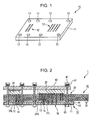
- FIG. 1 illustrates an exemplary circuit board 10 according to the embodiment.
- the circuit board 10 includes a plate member 11 and a circuit provided on the plate member 11.
- the plate member 11 of the circuit board 10 includes terminals 12 provided on a surface thereof, and holes 13.
- the plate member 11 is capable of holding a printed circuit board, electronic components mounted on the printed circuit board, and a cooling member provided over the electronic components, with the printed circuit board and the electronic components being positioned between the plate member 11 and the cooling member.
- the terminals 12 are conductive members that allow connection-object terminals provided on the printed circuit board carrying the electronic components and the circuit provided on the plate member 11 to be connected to each other.
- the terminals 12 are spring-like members that are elastically deformable.
- FIG. 2 illustrates an exemplary electronic apparatus 1 including the circuit board 10 according to the embodiment.
- the electronic apparatus 1 includes a printed circuit board 30 on which electronic components 20 that dissipate heat are mounted, and a heat sink 40 (an example of "cooling member" according to the present disclosure) provided over the electronic components 20.
- the printed circuit board 30 with the electronic components 20 mounted thereon is held between the circuit board 10 and the heat sink 40 provided over the electronic components 20.
- the printed circuit board 30 includes a circuit 33 including large-diameter vias 31L, small-diameter vias 31S, and wiring layers 32.
- the circuit 33 is designed such that a current flowing through the large-diameter vias 31L is higher than a current flowing through the small-diameter vias 31S.
- the circuit board 10 includes vias 14 provided at positions corresponding to the large-diameter vias 31L provided in the printed circuit board 30.
- the terminals 12 allow the vias 14 to be electrically connected with the large-diameter vias 31L.
- the vias 14 are also electrically connected with a wiring layer 15 embedded in the plate member 11 of the circuit board 10.
- the wiring layer 15 of the circuit board 10 is made of conductive plate or foil that is thicker than each of the wiring layers 32 of the printed circuit board 30. Hence, a circuit 16 including the vias 14 and the wiring layer 15 provided in the circuit board 10 may bear a higher current than the circuit 33 included in the printed circuit board 30.
- the circuit board 10 is fixed with bolts 41 that fasten the heat sink 40 and the plate member 11 together.
- a compression spring 42 that exerts a repulsive force when compressed is provided around a head-side part of each of the bolts 41.
- a nut 43 is screwed on the end of each of the bolts 41.
- the compression springs 42 through which the respective bolts 41 extend urge the heat sink 40 toward the printed circuit board 30.
- the heat sink 40 thus urged by the compression springs 42 is in close contact with the electronic components 20 on the printed circuit board 30. Since the heat sink 40 is in close contact with the electronic components 20, the heat dissipated from the electronic components 20 is effectively transferred to the heat sink 40.
- the bolts 41 extend through the respective holes 13 provided in the plate member 11.
- the repulsive forces exerted by the compression springs 42 that urge the heat sink 40 toward the printed circuit board 30 act on the heads of the respective bolts 41.
- the circuit board 10 receives a force that urges the circuit board 10 toward the printed circuit board 30 from the nuts 43 screwed on the respective bolts 41. Consequently, the terminals 12 provided on the plate member 11 are pressed against the printed circuit board 30, whereby the circuit 16 of the circuit board 10 is electrically connected with the circuit 33 of the printed circuit board 30.
- Spacers 44 are interposed between the circuit board 10 and the printed circuit board 30.
- the spacers 44 are each an annular member through which a corresponding one of the bolts 41 extends. The spacers 44 adjust the gap between the circuit board 10 and the printed circuit board 30 to such an extent that the elastically deformable terminals 12 are not squashed.
- FIG. 3 illustrates an exemplary electronic apparatus 101 according to a first comparative example.
- the electronic apparatus 101 according to the first comparative example includes a printed circuit board 130.
- the printed circuit board 130 includes a plurality of wiring layers 132S and 132L and electronic components 20 are mounted on the printed circuit board 130.
- the printed circuit board 130 includes a mixture of the wiring layer 132L that is for high current and the wiring layers 132S that are for low current.
- the wiring layer 132L for high current is made of a conductive plate or foil that is thicker than each of the wiring layers 132S for low current.
- via holes in which vias 131L for high current and vias 131S for low current are to be formed are provided in the printed circuit board 130 including the wiring layer 132L for high current by using a drill
- the drill may be broken.
- a small-diameter drill used in providing via holes intended for the formation of the vias 131S for low current has a lower strength than a large-diameter drill used in providing via holes intended for the formation of the vias 131L for high current.
- the strength of the drill is reduced as the diameter of the via hole to be provided is reduced.
- a drill having a low strength is less capable of drilling through the thick wiring layer 132L for high current.
- the electronic apparatus 101 according to the first comparative example has a trade-off between the increase in the thickness of the wiring layer 132L that occurs with the increase in the current supplied to the electronic components 20 and the reduction in the diameter of the vias 131S that occurs with the increase in the packaging density and the transmission speed of the electronic components 20.
- the electronic apparatus 101 according to the first comparative example it is difficult to realize both the increase in the current supplied to the electronic components 20 and the increase in the packaging density and the transmission speed of the electronic components 20.
- FIG. 4 illustrates an exemplary electronic apparatus 101' according to a second comparative example.
- the electronic apparatus 101' according to the second comparative example differs from the electronic apparatus 101 according to the first comparative example in including a printed circuit board 130' that includes only the wiring layers 132S for low current, unlike the printed circuit board 130. That is, the printed circuit board 130' of the electronic apparatus 101' according to the second comparative example does not include any wiring layer that corresponds to the wiring layer 132L for high current provided in the printed circuit board 130 of the electronic apparatus 101 according to the first comparative example. Instead, the printed circuit board 130' includes a bus bar 134 provided at a position where a high current flows, whereby the lack of thickness corresponding to the wiring layers 132S is compensated for.
- the bus bar 134 has to be provided at a position that does not overlap the area where the electronic components 20 are mounted, as illustrated in FIG. 4 . Such a situation increases the resistance loss in the current flowing from the area where the electronic components 20 are mounted to the position where the bus bar 134 is provided.
- FIG. 5 illustrates an exemplary electronic apparatus 101" according to a third comparative example.
- the electronic apparatus 101" according to the third comparative example includes a printed circuit board 130A" including wiring layers 132S for low current, and a printed circuit board 130B" including a wiring layer 132L for high current.
- the printed circuit board 130B" is joined to the printed circuit board 130A".
- Vias 131LA for high current provided in the printed circuit board 130A" allow a circuit 133B" provided in the printed circuit board 130B" to be electrically connected with the electronic components 20.
- vias 131SA for low current are provided only in the printed circuit board 130A", which includes no wiring layers 132L for high current.
- the printed circuit board 130B" of the electronic apparatus 101" according to the third comparative example is provided as a matter of convenience of drilling performed in providing the via holes. That is, the number of components of the electronic apparatus 101" is increased for the convenience of drilling.
- wiring lines for low current are provided as the circuit 33 of the printed circuit board 30, and wiring lines for high current are provided as the circuit 16 of the circuit board 10, which is separate from the printed circuit board 30.
- via holes intended for the formation of the small-diameter vias 31S for low current may be easily provided in the printed circuit board 30 by using a small-diameter drill that is unbearable in the drilling of the wiring layer 15 for high current provided in the circuit board 10.
- no bus bar intended for small-diameter vias are provided.
- the circuit board 10 also functions as a bolster plate that is provided in correspondence with the heat sink in the related art.
- the bolster plate provided in the related-art electronic apparatus may be omitted, avoiding the increase in the number of components of the electronic apparatus 1.
- the circuit board 10 and the electronic apparatus 1 according to the embodiment may each include electronic components that are operable with an increased current, at an increased packaging density, and at an increased transmission speed on the printed circuit board 30, which may be processed more easily than the printed circuit boards 130, 130', and 130" of the electronic apparatuses 101, 101', and 101" according to the first to third comparative examples.
- the circuit board 10 including the wiring layer 15 for high current is suitable as, for example, a power supply mechanism that supplies power to the printed circuit board 30 including the electronic components 20.
- the circuit board 10 is not limited to such a power supply mechanism.
- the circuit 16 of the circuit board 10 may perform a processing for a current signal similar to that performed by the circuit 33 of the printed circuit board 30.
- the circuit board 10 functions as a bolster plate that is provided in correspondence with the heat sink in the related art. Therefore, the plate member 11 included in the circuit board 10 is preferably rigid enough to bear deformation that may occur in the state where the printed circuit board 30 is held between the circuit board 10 and the heat sink 40.
- the plate member 11 of the circuit board 10 is not limited to a plate member that is so rigid as not to undergo any deformation under, for example, any load generated by a spring X.
- the plate member 11 of the circuit board 10 preferably has such a rigidity that the amount of deformation of the plate member 11 falls within a range in which the printed circuit board 30 that has received a load is not damaged.
- the circuit board 10 illustrated in FIG. 1 has a rectangular shape.
- the circuit board 10 according to the embodiment is not limited to a rectangular board.
- the circuit board 10 may have any other shape such as a square shape, a circular shape, an elliptical shape, a diamond shape, a polygonal shape, and so forth.
- the circuit board 10 illustrated in FIG. 1 includes the terminals 12 that are concentratedly arranged in two areas on the surface of the plate member 11.
- the circuit board 10 according to the embodiment is not limited to such a circuit board including the terminals 12 that are concentratedly arranged in two areas on the surface of the plate member 11 as an example.
- the circuit board 10 preferably includes terminals 12 that are arranged in correspondence with the pattern of wiring lines included in the printed circuit board 30 to be joined to the circuit board 10.
- the circuit board 10 illustrated in FIG. 1 includes eight holes 13 provided at edges of the plate member 11.
- the circuit board 10 according to the embodiment is not limited to such a circuit board having eight holes 13 provided at edges of the plate member 11.
- the circuit board 10 preferably includes an appropriate number of holes 13 provided in correspondence with the positions of holes that are provided in the heat sink 40 and that receive the respective bolts 41.
- the electronic apparatus 1 according to the embodiment includes one circuit board 10.
- the electronic apparatus 1 according to the embodiment is not limited to an electronic apparatus including one circuit board 10, and may include two or more circuit boards 10.
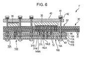
- FIG. 6 illustrates an exemplary electronic apparatus 1' according to a modification.
- the electronic apparatus 1' according to the modification includes two circuit boards 10A and 10B that are joined to the back side of a printed circuit board 30'.
- the printed circuit board 30' of the electronic apparatus 1' according to the modification includes a circuit 33'.
- the circuit 33' includes large-diameter vias 31L, medium-diameter vias 31M, small-diameter vias 31S, and wiring layers 32.
- the circuit 33' is designed such that a current flowing through the large-diameter vias 31L is higher than a current flowing through the medium-diameter vias 31M, and a current flowing through the medium-diameter vias 31M is larger than a current flowing through the small-diameter vias 31S.
- the circuit board 10A which is nearer to the printed circuit board 30' than the circuit board 10B, includes large-diameter vias 14LA at positions corresponding to the large-diameter vias 31L provided in the printed circuit board 30', and medium-diameter vias 14MA at positions corresponding to the medium-diameter vias 31M provided in the printed circuit board 30'.
- the large-diameter vias 14LA and the medium-diameter vias 14MA are allowed to be electrically connected with the large-diameter vias 31L and the medium-diameter vias 31M, respectively, by the terminals 12.
- the large-diameter vias 14LA and the medium-diameter vias 14MA are also electrically connected with a wiring layer 15A embedded in a plate member 11A included in the circuit board 10A.
- the circuit board 10B which is farther from the printed circuit board 30' than the circuit board 10A, includes large-diameter vias 14LB at positions corresponding to the large-diameter vias 31L provided in the printed circuit board 30'.
- the large-diameter vias 14LB are allowed to be electrically connected with the large-diameter vias 31L of the printed circuit board 30' by the terminals 12 and the large-diameter vias 14LA.
- the large-diameter vias 14LB are also electrically connected with a wiring layer 15B embedded in a plate member 11B included in the circuit board 10B.
- wiring lines for low current may be achieved by the circuit 33' included in the printed circuit board 30'
- wiring lines for medium current may be achieved by a circuit 16A included in the circuit board 10A
- wiring lines for high current may be achieved by a circuit 16B included in the circuit board 10B.
- via holes intended for the formation of the small-diameter vias 31S for low current may be easily provided in the printed circuit board 30' by using a small-diameter drill that is unbearable in the drilling of the wiring layer 15B for high current provided in the circuit board 10B.
- via holes intended for the formation of the medium-diameter vias 31M for medium current may be easily provided in the circuit board 10A by using a medium-diameter drill that is unbearable in the drilling of the wiring layer 15B for high current provided in the circuit board 10B. That is, when two or more circuit boards, such as the circuit boards 10A and 10B, are provided as in the case of the electronic apparatus 1' according to the modification, an electronic apparatus including circuits through which various levels of currents flow may be provided.
Landscapes
- Engineering & Computer Science (AREA)
- Microelectronics & Electronic Packaging (AREA)
- Structure Of Printed Boards (AREA)
- Production Of Multi-Layered Print Wiring Board (AREA)
- Combinations Of Printed Boards (AREA)
Abstract
Description
- The embodiment discussed herein is related to a circuit board and an electronic apparatus.
- The electric current supplied to electronic components mounted on a board, and the packaging density and the transmission speed of such electronic components have been increasing. In recent years, several improved techniques of mounting electronic components on a board have been proposed (see Japanese Laid-open Patent Publications No.
2006-66729 2003-174242 2006-253580 - Increasing the size of wiring lines provided on a board carrying electronic components makes it difficult to increase the packaging density and the transmission speed of the electronic components. To increase the electric current supplied to electronic components while increasing the packaging density and the transmission speed of the electronic components, the thickness of the wiring lines on the board may be increased, for example. However, increasing the thickness of the wiring lines on the board makes it difficult to form a circuit. For example, suppose that a via hole, whose diameter is reduced as the packaging density and the transmission speed increase, is to be formed in a wiring line by using a drill. In such a case, when the wiring line is thick, the drill tends to be broken.
- Accordingly, it is desirable to provide a circuit board and an electronic apparatus each including electronic components that are operable on a simply processed board with an increased current, at an increased packaging density, and at an increased transmission speed.
- According to an embodiment of an aspect of the invention, a circuit board includes a plate member capable of holding a printed circuit board, the printed circuit board including an electronic component, and a cooling member provided on the electronic component, the printed circuit board and the electronic component being positioned between the plate member and the cooling member; and a circuit provided to the plate member and allowed to be electrically connected with the printed circuit board.
-
-
FIG. 1 illustrates an exemplary circuit board according to an embodiment; -
FIG. 2 illustrates an exemplary electronic apparatus including the circuit board according to the embodiment; -
FIG. 3 illustrates an exemplary electronic apparatus according to a first comparative example; -
FIG. 4 illustrates an exemplary electronic apparatus according to a second comparative example; -
FIG. 5 illustrates an exemplary electronic apparatus according to a third comparative example; and -
FIG. 6 illustrates an exemplary electronic apparatus according to a modification. - Hereinafter, an embodiment will be described. The following embodiment is only exemplary and does not limit the technical scope of the present disclosure.
-
FIG. 1 illustrates anexemplary circuit board 10 according to the embodiment. Thecircuit board 10 includes aplate member 11 and a circuit provided on theplate member 11. Theplate member 11 of thecircuit board 10 includesterminals 12 provided on a surface thereof, andholes 13. Theplate member 11 is capable of holding a printed circuit board, electronic components mounted on the printed circuit board, and a cooling member provided over the electronic components, with the printed circuit board and the electronic components being positioned between theplate member 11 and the cooling member. Theterminals 12 are conductive members that allow connection-object terminals provided on the printed circuit board carrying the electronic components and the circuit provided on theplate member 11 to be connected to each other. Theterminals 12 are spring-like members that are elastically deformable. -
FIG. 2 illustrates an exemplary electronic apparatus 1 including thecircuit board 10 according to the embodiment. The electronic apparatus 1 includes a printedcircuit board 30 on whichelectronic components 20 that dissipate heat are mounted, and a heat sink 40 (an example of "cooling member" according to the present disclosure) provided over theelectronic components 20. The printedcircuit board 30 with theelectronic components 20 mounted thereon is held between thecircuit board 10 and theheat sink 40 provided over theelectronic components 20. The printedcircuit board 30 includes acircuit 33 including large-diameter vias 31L, small-diameter vias 31S, andwiring layers 32. Thecircuit 33 is designed such that a current flowing through the large-diameter vias 31L is higher than a current flowing through the small-diameter vias 31S. - As illustrated in
FIG. 2 as a sectional view of thecircuit board 10, thecircuit board 10 includesvias 14 provided at positions corresponding to the large-diameter vias 31L provided in the printedcircuit board 30. Theterminals 12 allow thevias 14 to be electrically connected with the large-diameter vias 31L. Thevias 14 are also electrically connected with awiring layer 15 embedded in theplate member 11 of thecircuit board 10. Thewiring layer 15 of thecircuit board 10 is made of conductive plate or foil that is thicker than each of thewiring layers 32 of the printedcircuit board 30. Hence, acircuit 16 including thevias 14 and thewiring layer 15 provided in thecircuit board 10 may bear a higher current than thecircuit 33 included in theprinted circuit board 30. - The
circuit board 10 is fixed withbolts 41 that fasten theheat sink 40 and theplate member 11 together. Acompression spring 42 that exerts a repulsive force when compressed is provided around a head-side part of each of thebolts 41. Anut 43 is screwed on the end of each of thebolts 41. The compression springs 42 through which therespective bolts 41 extend urge theheat sink 40 toward the printedcircuit board 30. Theheat sink 40 thus urged by thecompression springs 42 is in close contact with theelectronic components 20 on the printedcircuit board 30. Since theheat sink 40 is in close contact with theelectronic components 20, the heat dissipated from theelectronic components 20 is effectively transferred to theheat sink 40. - The
bolts 41 extend through therespective holes 13 provided in theplate member 11. The repulsive forces exerted by thecompression springs 42 that urge theheat sink 40 toward the printedcircuit board 30 act on the heads of therespective bolts 41. Accordingly, thecircuit board 10 receives a force that urges thecircuit board 10 toward theprinted circuit board 30 from thenuts 43 screwed on therespective bolts 41. Consequently, theterminals 12 provided on theplate member 11 are pressed against the printedcircuit board 30, whereby thecircuit 16 of thecircuit board 10 is electrically connected with thecircuit 33 of the printedcircuit board 30.Spacers 44 are interposed between thecircuit board 10 and the printedcircuit board 30. Thespacers 44 are each an annular member through which a corresponding one of thebolts 41 extends. Thespacers 44 adjust the gap between thecircuit board 10 and the printedcircuit board 30 to such an extent that the elasticallydeformable terminals 12 are not squashed. -
FIG. 3 illustrates an exemplaryelectronic apparatus 101 according to a first comparative example. Theelectronic apparatus 101 according to the first comparative example includes a printedcircuit board 130. The printedcircuit board 130 includes a plurality ofwiring layers electronic components 20 are mounted on the printedcircuit board 130. The printedcircuit board 130 includes a mixture of thewiring layer 132L that is for high current and thewiring layers 132S that are for low current. Thewiring layer 132L for high current is made of a conductive plate or foil that is thicker than each of thewiring layers 132S for low current. When via holes in which vias 131L for high current andvias 131S for low current are to be formed are provided in the printedcircuit board 130 including thewiring layer 132L for high current by using a drill, the drill may be broken. Specifically, a small-diameter drill used in providing via holes intended for the formation of thevias 131S for low current has a lower strength than a large-diameter drill used in providing via holes intended for the formation of thevias 131L for high current. The strength of the drill is reduced as the diameter of the via hole to be provided is reduced. A drill having a low strength is less capable of drilling through thethick wiring layer 132L for high current. That is, theelectronic apparatus 101 according to the first comparative example has a trade-off between the increase in the thickness of thewiring layer 132L that occurs with the increase in the current supplied to theelectronic components 20 and the reduction in the diameter of thevias 131S that occurs with the increase in the packaging density and the transmission speed of theelectronic components 20. Hence, in theelectronic apparatus 101 according to the first comparative example, it is difficult to realize both the increase in the current supplied to theelectronic components 20 and the increase in the packaging density and the transmission speed of theelectronic components 20. -
FIG. 4 illustrates an exemplary electronic apparatus 101' according to a second comparative example. The electronic apparatus 101' according to the second comparative example differs from theelectronic apparatus 101 according to the first comparative example in including a printed circuit board 130' that includes only thewiring layers 132S for low current, unlike the printedcircuit board 130. That is, the printed circuit board 130' of the electronic apparatus 101' according to the second comparative example does not include any wiring layer that corresponds to thewiring layer 132L for high current provided in the printedcircuit board 130 of theelectronic apparatus 101 according to the first comparative example. Instead, the printed circuit board 130' includes abus bar 134 provided at a position where a high current flows, whereby the lack of thickness corresponding to thewiring layers 132S is compensated for. Nevertheless, to maintain the packaging density and the transmission speed of theelectronic components 20, thebus bar 134 has to be provided at a position that does not overlap the area where theelectronic components 20 are mounted, as illustrated inFIG. 4 . Such a situation increases the resistance loss in the current flowing from the area where theelectronic components 20 are mounted to the position where thebus bar 134 is provided. -
FIG. 5 illustrates an exemplaryelectronic apparatus 101" according to a third comparative example. Theelectronic apparatus 101" according to the third comparative example includes a printedcircuit board 130A" includingwiring layers 132S for low current, and a printedcircuit board 130B" including awiring layer 132L for high current. The printedcircuit board 130B" is joined to the printedcircuit board 130A". Vias 131LA for high current provided in the printedcircuit board 130A" allow acircuit 133B" provided in the printedcircuit board 130B" to be electrically connected with theelectronic components 20. In theelectronic apparatus 101" according to the third comparative example, vias 131SA for low current are provided only in the printedcircuit board 130A", which includes no wiring layers 132L for high current. Hence, there is no need for a small-diameter drill used for forming the vias 131SA to penetrate through thewiring layer 132L for high current. In such a case, the printedcircuit board 130B" of theelectronic apparatus 101" according to the third comparative example is provided as a matter of convenience of drilling performed in providing the via holes. That is, the number of components of theelectronic apparatus 101" is increased for the convenience of drilling. - In contrast, in the
circuit board 10 and the electronic apparatus 1 according to the embodiment, wiring lines for low current are provided as thecircuit 33 of the printedcircuit board 30, and wiring lines for high current are provided as thecircuit 16 of thecircuit board 10, which is separate from the printedcircuit board 30. Hence, via holes intended for the formation of the small-diameter vias 31S for low current may be easily provided in the printedcircuit board 30 by using a small-diameter drill that is unbearable in the drilling of thewiring layer 15 for high current provided in thecircuit board 10. Moreover, no bus bar intended for small-diameter vias are provided. In addition, thecircuit board 10 also functions as a bolster plate that is provided in correspondence with the heat sink in the related art. Hence, the bolster plate provided in the related-art electronic apparatus may be omitted, avoiding the increase in the number of components of the electronic apparatus 1. Thus, thecircuit board 10 and the electronic apparatus 1 according to the embodiment may each include electronic components that are operable with an increased current, at an increased packaging density, and at an increased transmission speed on the printedcircuit board 30, which may be processed more easily than the printedcircuit boards electronic apparatuses - The
circuit board 10 including thewiring layer 15 for high current is suitable as, for example, a power supply mechanism that supplies power to the printedcircuit board 30 including theelectronic components 20. Thecircuit board 10 is not limited to such a power supply mechanism. Thecircuit 16 of thecircuit board 10 may perform a processing for a current signal similar to that performed by thecircuit 33 of the printedcircuit board 30. - The
circuit board 10 according to the embodiment functions as a bolster plate that is provided in correspondence with the heat sink in the related art. Therefore, theplate member 11 included in thecircuit board 10 is preferably rigid enough to bear deformation that may occur in the state where the printedcircuit board 30 is held between thecircuit board 10 and theheat sink 40. However, theplate member 11 of thecircuit board 10 is not limited to a plate member that is so rigid as not to undergo any deformation under, for example, any load generated by a spring X. Theplate member 11 of thecircuit board 10 preferably has such a rigidity that the amount of deformation of theplate member 11 falls within a range in which the printedcircuit board 30 that has received a load is not damaged. - The
circuit board 10 illustrated inFIG. 1 has a rectangular shape. Thecircuit board 10 according to the embodiment is not limited to a rectangular board. Thecircuit board 10 may have any other shape such as a square shape, a circular shape, an elliptical shape, a diamond shape, a polygonal shape, and so forth. - The
circuit board 10 illustrated inFIG. 1 includes theterminals 12 that are concentratedly arranged in two areas on the surface of theplate member 11. Thecircuit board 10 according to the embodiment is not limited to such a circuit board including theterminals 12 that are concentratedly arranged in two areas on the surface of theplate member 11 as an example. Thecircuit board 10 preferably includesterminals 12 that are arranged in correspondence with the pattern of wiring lines included in the printedcircuit board 30 to be joined to thecircuit board 10. - The
circuit board 10 illustrated inFIG. 1 includes eightholes 13 provided at edges of theplate member 11. Thecircuit board 10 according to the embodiment is not limited to such a circuit board having eightholes 13 provided at edges of theplate member 11. Thecircuit board 10 preferably includes an appropriate number ofholes 13 provided in correspondence with the positions of holes that are provided in theheat sink 40 and that receive therespective bolts 41. - The electronic apparatus 1 according to the embodiment includes one
circuit board 10. The electronic apparatus 1 according to the embodiment is not limited to an electronic apparatus including onecircuit board 10, and may include two ormore circuit boards 10.FIG. 6 illustrates an exemplary electronic apparatus 1' according to a modification. The electronic apparatus 1' according to the modification includes twocircuit boards diameter vias 31L, medium-diameter vias 31M, small-diameter vias 31S, and wiring layers 32. The circuit 33' is designed such that a current flowing through the large-diameter vias 31L is higher than a current flowing through the medium-diameter vias 31M, and a current flowing through the medium-diameter vias 31M is larger than a current flowing through the small-diameter vias 31S. - The
circuit board 10A, which is nearer to the printed circuit board 30' than thecircuit board 10B, includes large-diameter vias 14LA at positions corresponding to the large-diameter vias 31L provided in the printed circuit board 30', and medium-diameter vias 14MA at positions corresponding to the medium-diameter vias 31M provided in the printed circuit board 30'. The large-diameter vias 14LA and the medium-diameter vias 14MA are allowed to be electrically connected with the large-diameter vias 31L and the medium-diameter vias 31M, respectively, by theterminals 12. The large-diameter vias 14LA and the medium-diameter vias 14MA are also electrically connected with awiring layer 15A embedded in aplate member 11A included in thecircuit board 10A. - The
circuit board 10B, which is farther from the printed circuit board 30' than thecircuit board 10A, includes large-diameter vias 14LB at positions corresponding to the large-diameter vias 31L provided in the printed circuit board 30'. The large-diameter vias 14LB are allowed to be electrically connected with the large-diameter vias 31L of the printed circuit board 30' by theterminals 12 and the large-diameter vias 14LA. The large-diameter vias 14LB are also electrically connected with awiring layer 15B embedded in aplate member 11B included in thecircuit board 10B. - When two or more circuit boards, such as the
circuit boards circuit 16A included in thecircuit board 10A, and wiring lines for high current may be achieved by acircuit 16B included in thecircuit board 10B. Hence, via holes intended for the formation of the small-diameter vias 31S for low current may be easily provided in the printed circuit board 30' by using a small-diameter drill that is unbearable in the drilling of thewiring layer 15B for high current provided in thecircuit board 10B. Furthermore, via holes intended for the formation of the medium-diameter vias 31M for medium current may be easily provided in thecircuit board 10A by using a medium-diameter drill that is unbearable in the drilling of thewiring layer 15B for high current provided in thecircuit board 10B. That is, when two or more circuit boards, such as thecircuit boards
Claims (10)
- A circuit board comprising:a plate member capable of holding a printed circuit board, the printed circuit board including an electronic component, and a cooling member provided on the electronic component, the printed circuit board and the electronic component being positioned between the plate member and the cooling member; anda circuit provided to the plate member and allowed to be electrically connected with the printed circuit board.
- The circuit board according to claim 1, wherein a terminal that allows a connection-object terminal provided on the printed circuit board and the circuit to be connected to each other is provided on a surface of the plate member.
- The circuit board according to claim 2, wherein the terminal that allows the connection-object terminal provided on the printed circuit board and the circuit to be connected to each other is elastically deformable.
- The circuit board according to any of claims 1 to 3, wherein the plate member includes a hole through which a fastening member that fastens the cooling member and the plate member together is allowed to extend.
- The circuit board according to any of claims 1 to 4, wherein the circuit is made of one of a conductive plate and conductive foil, the one of the conductive plate and the conductive foil being thicker than a circuit included in the printed circuit board.
- An electronic apparatus comprising:a printed circuit board on which an electronic component is mounted;a cooling member provided on the electronic component; anda circuit board includinga plate member configured to hold the printed circuit board and the electronic component, the printed circuit board and the electronic component being positioned between the plate member and the cooling member, anda circuit provided to the plate member and that is electrically connected with the printed circuit board.
- The electronic apparatus according to claim 6, wherein a terminal that connects a connection-object terminal provided on the printed circuit board and the circuit to each other is provided on a surface of the plate member.
- The electronic apparatus according to claim 7, wherein the terminal that connects the connection-object terminal provided on the printed circuit board and the circuit to each other is elastically deformable.
- The electronic apparatus according to any of claims 6 to 8, wherein the plate member includes a hole through which a fastening member that fastens the cooling member and the plate member together extends.
- The electronic apparatus according to any of claims 6 to 9, wherein the circuit is made of one of a conductive plate and conductive foil, the one of the conductive plate and the conductive foil being thicker than a circuit included in the printed circuit board.
Applications Claiming Priority (1)
| Application Number | Priority Date | Filing Date | Title |
|---|---|---|---|
| JP2014164664A JP6421491B2 (en) | 2014-08-13 | 2014-08-13 | Electronics |
Publications (1)
| Publication Number | Publication Date |
|---|---|
| EP2991461A1 true EP2991461A1 (en) | 2016-03-02 |
Family
ID=53682607
Family Applications (1)
| Application Number | Title | Priority Date | Filing Date |
|---|---|---|---|
| EP15177921.2A Withdrawn EP2991461A1 (en) | 2014-08-13 | 2015-07-22 | Circuit board and electronic apparatus |
Country Status (3)
| Country | Link |
|---|---|
| US (1) | US9867274B2 (en) |
| EP (1) | EP2991461A1 (en) |
| JP (1) | JP6421491B2 (en) |
Cited By (2)
| Publication number | Priority date | Publication date | Assignee | Title |
|---|---|---|---|---|
| CN110972394A (en) * | 2019-12-31 | 2020-04-07 | 中科可控信息产业有限公司 | Circuit board structure and electronic equipment |
| WO2020180341A1 (en) * | 2019-03-06 | 2020-09-10 | Ttm Technologies, Inc. | Methods for fabricating printed circuit board assemblies with high density via array |
Families Citing this family (8)
| Publication number | Priority date | Publication date | Assignee | Title |
|---|---|---|---|---|
| JP2018107307A (en) * | 2016-12-27 | 2018-07-05 | 富士通株式会社 | Printed circuit board and electronic device |
| DE102017221861A1 (en) * | 2017-12-05 | 2019-06-06 | Zf Friedrichshafen Ag | Printed circuit board and method for manufacturing a printed circuit board |
| US11508663B2 (en) * | 2018-02-02 | 2022-11-22 | Marvell Israel (M.I.S.L) Ltd. | PCB module on package |
| US11011451B2 (en) * | 2018-12-05 | 2021-05-18 | Taiwan Semiconductor Manufacturing Company, Ltd. | Integrated circuit package and method |
| WO2020250162A1 (en) | 2019-06-10 | 2020-12-17 | Marvell Israel (M.I.S.L) Ltd. | Ic package with top-side memory module |
| US11444002B2 (en) * | 2020-07-29 | 2022-09-13 | Taiwan Semiconductor Manufacturing Company, Ltd. | Package structure |
| JP2025131949A (en) * | 2022-08-08 | 2025-09-10 | 株式会社Ihi | Board fixing structure |
| CN115442954A (en) * | 2022-08-17 | 2022-12-06 | 华为数字能源技术有限公司 | A circuit board assembly and electronic equipment |
Citations (6)
| Publication number | Priority date | Publication date | Assignee | Title |
|---|---|---|---|---|
| JP2003174242A (en) | 2001-12-06 | 2003-06-20 | Shindengen Electric Mfg Co Ltd | Electronic circuit device and method for manufacturing it |
| US20040212964A1 (en) * | 2003-04-28 | 2004-10-28 | Belady Christian L. | Stack up assembly |
| US20040264114A1 (en) * | 2003-05-30 | 2004-12-30 | Kabushiki Kaisha Toshiba | Electronic apparatus including printed wiring board provided with heat generating component |
| JP2006066729A (en) | 2004-08-27 | 2006-03-09 | Toshiba Corp | Circuit board module and manufacturing method thereof |
| JP2006253580A (en) | 2005-03-14 | 2006-09-21 | Alps Electric Co Ltd | Electronic function component packaging body and electronic apparatus |
| WO2014074045A1 (en) * | 2012-11-06 | 2014-05-15 | Telefonaktiebolaget L M Ericsson (Publ) | Heat dissipation assembly |
Family Cites Families (16)
| Publication number | Priority date | Publication date | Assignee | Title |
|---|---|---|---|---|
| JPH062287Y2 (en) * | 1989-03-16 | 1994-01-19 | 日立電線株式会社 | High current wiring board unit |
| US5305185A (en) * | 1992-09-30 | 1994-04-19 | Samarov Victor M | Coplanar heatsink and electronics assembly |
| DE69401040T2 (en) * | 1993-07-12 | 1997-06-05 | Nippon Electric Co | Housing structure for microwave switching |
| US5390078A (en) * | 1993-08-30 | 1995-02-14 | At&T Global Information Solutions Company | Apparatus for using an active circuit board as a heat sink |
| US5557503A (en) * | 1995-05-12 | 1996-09-17 | International Business Machines Corporation | Circuit card having a large module strain relief and heat sink support |
| US20030214800A1 (en) * | 1999-07-15 | 2003-11-20 | Dibene Joseph Ted | System and method for processor power delivery and thermal management |
| US6847529B2 (en) * | 1999-07-15 | 2005-01-25 | Incep Technologies, Inc. | Ultra-low impedance power interconnection system for electronic packages |
| US6856007B2 (en) * | 2001-08-28 | 2005-02-15 | Tessera, Inc. | High-frequency chip packages |
| JP4036742B2 (en) * | 2002-09-18 | 2008-01-23 | 富士通株式会社 | Package structure, printed circuit board on which the package structure is mounted, and electronic apparatus having the printed circuit board |
| JP4393312B2 (en) * | 2004-08-27 | 2010-01-06 | 富士通株式会社 | Semiconductor device |
| JP4744360B2 (en) * | 2006-05-22 | 2011-08-10 | 富士通株式会社 | Semiconductor device |
| DE102006025453B4 (en) * | 2006-05-31 | 2009-12-24 | Infineon Technologies Ag | Semiconductor circuitry |
| JP4985779B2 (en) * | 2007-10-24 | 2012-07-25 | 富士通株式会社 | Printed circuit board unit and socket |
| JP2010087044A (en) * | 2008-09-29 | 2010-04-15 | Toshiba Corp | Electronic apparatus |
| JP2010263118A (en) * | 2009-05-08 | 2010-11-18 | Fuzhun Precision Industry (Shenzhen) Co Ltd | Heat dissipation device |
| JP2011065802A (en) * | 2009-09-16 | 2011-03-31 | Nec Saitama Ltd | Stacking connector and method of manufacturing the same |
-
2014
- 2014-08-13 JP JP2014164664A patent/JP6421491B2/en active Active
-
2015
- 2015-07-21 US US14/804,748 patent/US9867274B2/en active Active
- 2015-07-22 EP EP15177921.2A patent/EP2991461A1/en not_active Withdrawn
Patent Citations (6)
| Publication number | Priority date | Publication date | Assignee | Title |
|---|---|---|---|---|
| JP2003174242A (en) | 2001-12-06 | 2003-06-20 | Shindengen Electric Mfg Co Ltd | Electronic circuit device and method for manufacturing it |
| US20040212964A1 (en) * | 2003-04-28 | 2004-10-28 | Belady Christian L. | Stack up assembly |
| US20040264114A1 (en) * | 2003-05-30 | 2004-12-30 | Kabushiki Kaisha Toshiba | Electronic apparatus including printed wiring board provided with heat generating component |
| JP2006066729A (en) | 2004-08-27 | 2006-03-09 | Toshiba Corp | Circuit board module and manufacturing method thereof |
| JP2006253580A (en) | 2005-03-14 | 2006-09-21 | Alps Electric Co Ltd | Electronic function component packaging body and electronic apparatus |
| WO2014074045A1 (en) * | 2012-11-06 | 2014-05-15 | Telefonaktiebolaget L M Ericsson (Publ) | Heat dissipation assembly |
Cited By (4)
| Publication number | Priority date | Publication date | Assignee | Title |
|---|---|---|---|---|
| WO2020180341A1 (en) * | 2019-03-06 | 2020-09-10 | Ttm Technologies, Inc. | Methods for fabricating printed circuit board assemblies with high density via array |
| US10980127B2 (en) | 2019-03-06 | 2021-04-13 | Ttm Technologies Inc. | Methods for fabricating printed circuit board assemblies with high density via array |
| CN110972394A (en) * | 2019-12-31 | 2020-04-07 | 中科可控信息产业有限公司 | Circuit board structure and electronic equipment |
| CN110972394B (en) * | 2019-12-31 | 2021-03-23 | 中科可控信息产业有限公司 | Circuit board structure and electronic equipment |
Also Published As
| Publication number | Publication date |
|---|---|
| JP6421491B2 (en) | 2018-11-14 |
| US20160050743A1 (en) | 2016-02-18 |
| JP2016040806A (en) | 2016-03-24 |
| US9867274B2 (en) | 2018-01-09 |
Similar Documents
| Publication | Publication Date | Title |
|---|---|---|
| EP2991461A1 (en) | Circuit board and electronic apparatus | |
| US6580611B1 (en) | Dual-sided heat removal system | |
| EP2561733B1 (en) | Wedge lock for use with a single board computer, a single board computer, and method of assembling a computer system | |
| US10199904B2 (en) | Cooling a heat-generating electronic device | |
| EP2525632B1 (en) | Systems for circuit board heat transfer and method of assembling same | |
| US9769916B2 (en) | Printed circuit board and electronic device | |
| KR20120117850A (en) | Thermal plug for use with a heat sink and method of assembling same | |
| US7902464B2 (en) | Heat sink arrangement for electrical apparatus | |
| JP4687430B2 (en) | Electronic device and manufacturing method thereof | |
| EP3853897B1 (en) | ELECTRONIC ASSEMBLY | |
| US10607917B2 (en) | Substrate | |
| US9553428B2 (en) | Power supply module | |
| US20210400839A1 (en) | Pressing Device | |
| US6324059B1 (en) | Apparatus and method for improving heat sink component capacity and efficiency | |
| WO2014075217A1 (en) | Radiator and heat dissipation system | |
| JP4961215B2 (en) | Power device device | |
| EP2200408B1 (en) | Circuit board device, in particular for an electric power consuming device in a motor vehicle | |
| JP6403741B2 (en) | Surface mount semiconductor package equipment | |
| US10306751B2 (en) | DDR electronic module assembly | |
| CN212628593U (en) | Connection structure and motor drive device | |
| JP2018176943A (en) | Electric power steering control device and electronic unit. | |
| JP6733934B2 (en) | Heat conductive flexible printed wiring board and method for manufacturing heat conductive flexible printed wiring board | |
| KR20050072257A (en) | Thermal pad using dlc coating | |
| HK1164633A (en) | Dual-sided heat removal system |
Legal Events
| Date | Code | Title | Description |
|---|---|---|---|
| PUAI | Public reference made under article 153(3) epc to a published international application that has entered the european phase |
Free format text: ORIGINAL CODE: 0009012 |
|
| AK | Designated contracting states |
Kind code of ref document: A1 Designated state(s): AL AT BE BG CH CY CZ DE DK EE ES FI FR GB GR HR HU IE IS IT LI LT LU LV MC MK MT NL NO PL PT RO RS SE SI SK SM TR |
|
| AX | Request for extension of the european patent |
Extension state: BA ME |
|
| 17P | Request for examination filed |
Effective date: 20160422 |
|
| RBV | Designated contracting states (corrected) |
Designated state(s): AL AT BE BG CH CY CZ DE DK EE ES FI FR GB GR HR HU IE IS IT LI LT LU LV MC MK MT NL NO PL PT RO RS SE SI SK SM TR |
|
| STAA | Information on the status of an ep patent application or granted ep patent |
Free format text: STATUS: THE APPLICATION HAS BEEN WITHDRAWN |
|
| 18W | Application withdrawn |
Effective date: 20171102 |