EP2988416A1 - Circuits and methods for 2g amplification using 3g/4g linear path combination - Google Patents
Circuits and methods for 2g amplification using 3g/4g linear path combination Download PDFInfo
- Publication number
- EP2988416A1 EP2988416A1 EP15181220.3A EP15181220A EP2988416A1 EP 2988416 A1 EP2988416 A1 EP 2988416A1 EP 15181220 A EP15181220 A EP 15181220A EP 2988416 A1 EP2988416 A1 EP 2988416A1
- Authority
- EP
- European Patent Office
- Prior art keywords
- amplification
- signal
- path
- end architecture
- paths
- Prior art date
- Legal status (The legal status is an assumption and is not a legal conclusion. Google has not performed a legal analysis and makes no representation as to the accuracy of the status listed.)
- Granted
Links
Images



Classifications
-
- H—ELECTRICITY
- H03—ELECTRONIC CIRCUITRY
- H03F—AMPLIFIERS
- H03F1/00—Details of amplifiers with only discharge tubes, only semiconductor devices or only unspecified devices as amplifying elements
- H03F1/02—Modifications of amplifiers to raise the efficiency, e.g. gliding Class A stages, use of an auxiliary oscillation
- H03F1/0205—Modifications of amplifiers to raise the efficiency, e.g. gliding Class A stages, use of an auxiliary oscillation in transistor amplifiers
- H03F1/0277—Selecting one or more amplifiers from a plurality of amplifiers
-
- H—ELECTRICITY
- H03—ELECTRONIC CIRCUITRY
- H03F—AMPLIFIERS
- H03F3/00—Amplifiers with only discharge tubes or only semiconductor devices as amplifying elements
- H03F3/189—High-frequency amplifiers, e.g. radio frequency amplifiers
- H03F3/19—High-frequency amplifiers, e.g. radio frequency amplifiers with semiconductor devices only
-
- H—ELECTRICITY
- H03—ELECTRONIC CIRCUITRY
- H03F—AMPLIFIERS
- H03F3/00—Amplifiers with only discharge tubes or only semiconductor devices as amplifying elements
- H03F3/189—High-frequency amplifiers, e.g. radio frequency amplifiers
- H03F3/19—High-frequency amplifiers, e.g. radio frequency amplifiers with semiconductor devices only
- H03F3/191—Tuned amplifiers
-
- H—ELECTRICITY
- H03—ELECTRONIC CIRCUITRY
- H03F—AMPLIFIERS
- H03F3/00—Amplifiers with only discharge tubes or only semiconductor devices as amplifying elements
- H03F3/189—High-frequency amplifiers, e.g. radio frequency amplifiers
- H03F3/19—High-frequency amplifiers, e.g. radio frequency amplifiers with semiconductor devices only
- H03F3/195—High-frequency amplifiers, e.g. radio frequency amplifiers with semiconductor devices only in integrated circuits
-
- H—ELECTRICITY
- H03—ELECTRONIC CIRCUITRY
- H03F—AMPLIFIERS
- H03F3/00—Amplifiers with only discharge tubes or only semiconductor devices as amplifying elements
- H03F3/20—Power amplifiers, e.g. Class B amplifiers, Class C amplifiers
- H03F3/21—Power amplifiers, e.g. Class B amplifiers, Class C amplifiers with semiconductor devices only
- H03F3/211—Power amplifiers, e.g. Class B amplifiers, Class C amplifiers with semiconductor devices only using a combination of several amplifiers
-
- H—ELECTRICITY
- H03—ELECTRONIC CIRCUITRY
- H03F—AMPLIFIERS
- H03F3/00—Amplifiers with only discharge tubes or only semiconductor devices as amplifying elements
- H03F3/20—Power amplifiers, e.g. Class B amplifiers, Class C amplifiers
- H03F3/21—Power amplifiers, e.g. Class B amplifiers, Class C amplifiers with semiconductor devices only
- H03F3/213—Power amplifiers, e.g. Class B amplifiers, Class C amplifiers with semiconductor devices only in integrated circuits
-
- H—ELECTRICITY
- H03—ELECTRONIC CIRCUITRY
- H03F—AMPLIFIERS
- H03F3/00—Amplifiers with only discharge tubes or only semiconductor devices as amplifying elements
- H03F3/20—Power amplifiers, e.g. Class B amplifiers, Class C amplifiers
- H03F3/24—Power amplifiers, e.g. Class B amplifiers, Class C amplifiers of transmitter output stages
- H03F3/245—Power amplifiers, e.g. Class B amplifiers, Class C amplifiers of transmitter output stages with semiconductor devices only
-
- H—ELECTRICITY
- H03—ELECTRONIC CIRCUITRY
- H03F—AMPLIFIERS
- H03F3/00—Amplifiers with only discharge tubes or only semiconductor devices as amplifying elements
- H03F3/72—Gated amplifiers, i.e. amplifiers which are rendered operative or inoperative by means of a control signal
-
- H—ELECTRICITY
- H04—ELECTRIC COMMUNICATION TECHNIQUE
- H04B—TRANSMISSION
- H04B1/00—Details of transmission systems, not covered by a single one of groups H04B3/00 - H04B13/00; Details of transmission systems not characterised by the medium used for transmission
- H04B1/005—Details of transmission systems, not covered by a single one of groups H04B3/00 - H04B13/00; Details of transmission systems not characterised by the medium used for transmission adapting radio receivers, transmitters andtransceivers for operation on two or more bands, i.e. frequency ranges
- H04B1/0053—Details of transmission systems, not covered by a single one of groups H04B3/00 - H04B13/00; Details of transmission systems not characterised by the medium used for transmission adapting radio receivers, transmitters andtransceivers for operation on two or more bands, i.e. frequency ranges with common antenna for more than one band
-
- H—ELECTRICITY
- H04—ELECTRIC COMMUNICATION TECHNIQUE
- H04B—TRANSMISSION
- H04B1/00—Details of transmission systems, not covered by a single one of groups H04B3/00 - H04B13/00; Details of transmission systems not characterised by the medium used for transmission
- H04B1/06—Receivers
- H04B1/16—Circuits
- H04B1/18—Input circuits, e.g. for coupling to an antenna or a transmission line
-
- H—ELECTRICITY
- H04—ELECTRIC COMMUNICATION TECHNIQUE
- H04B—TRANSMISSION
- H04B1/00—Details of transmission systems, not covered by a single one of groups H04B3/00 - H04B13/00; Details of transmission systems not characterised by the medium used for transmission
- H04B1/38—Transceivers, i.e. devices in which transmitter and receiver form a structural unit and in which at least one part is used for functions of transmitting and receiving
- H04B1/40—Circuits
- H04B1/401—Circuits for selecting or indicating operating mode
-
- H—ELECTRICITY
- H03—ELECTRONIC CIRCUITRY
- H03F—AMPLIFIERS
- H03F2200/00—Indexing scheme relating to amplifiers
- H03F2200/111—Indexing scheme relating to amplifiers the amplifier being a dual or triple band amplifier, e.g. 900 and 1800 MHz, e.g. switched or not switched, simultaneously or not
-
- H—ELECTRICITY
- H03—ELECTRONIC CIRCUITRY
- H03F—AMPLIFIERS
- H03F2200/00—Indexing scheme relating to amplifiers
- H03F2200/225—Indexing scheme relating to amplifiers the input circuit of an amplifying stage comprising an LC-network
-
- H—ELECTRICITY
- H03—ELECTRONIC CIRCUITRY
- H03F—AMPLIFIERS
- H03F2200/00—Indexing scheme relating to amplifiers
- H03F2200/231—Indexing scheme relating to amplifiers the input of an amplifier can be switched on or off by a switch to amplify or not an input signal
-
- H—ELECTRICITY
- H03—ELECTRONIC CIRCUITRY
- H03F—AMPLIFIERS
- H03F2200/00—Indexing scheme relating to amplifiers
- H03F2200/451—Indexing scheme relating to amplifiers the amplifier being a radio frequency amplifier
-
- H—ELECTRICITY
- H03—ELECTRONIC CIRCUITRY
- H03F—AMPLIFIERS
- H03F2200/00—Indexing scheme relating to amplifiers
- H03F2200/541—Transformer coupled at the output of an amplifier
-
- H—ELECTRICITY
- H03—ELECTRONIC CIRCUITRY
- H03F—AMPLIFIERS
- H03F2203/00—Indexing scheme relating to amplifiers with only discharge tubes or only semiconductor devices as amplifying elements covered by H03F3/00
- H03F2203/20—Indexing scheme relating to power amplifiers, e.g. Class B amplifiers, Class C amplifiers
- H03F2203/21—Indexing scheme relating to power amplifiers, e.g. Class B amplifiers, Class C amplifiers with semiconductor devices only
- H03F2203/211—Indexing scheme relating to power amplifiers, e.g. Class B amplifiers, Class C amplifiers with semiconductor devices only using a combination of several amplifiers
- H03F2203/21109—An input signal being distributed by switching to a plurality of paralleled power amplifiers
-
- H—ELECTRICITY
- H03—ELECTRONIC CIRCUITRY
- H03F—AMPLIFIERS
- H03F2203/00—Indexing scheme relating to amplifiers with only discharge tubes or only semiconductor devices as amplifying elements covered by H03F3/00
- H03F2203/20—Indexing scheme relating to power amplifiers, e.g. Class B amplifiers, Class C amplifiers
- H03F2203/21—Indexing scheme relating to power amplifiers, e.g. Class B amplifiers, Class C amplifiers with semiconductor devices only
- H03F2203/211—Indexing scheme relating to power amplifiers, e.g. Class B amplifiers, Class C amplifiers with semiconductor devices only using a combination of several amplifiers
- H03F2203/21139—An impedance adaptation circuit being added at the output of a power amplifier stage
-
- H—ELECTRICITY
- H03—ELECTRONIC CIRCUITRY
- H03F—AMPLIFIERS
- H03F2203/00—Indexing scheme relating to amplifiers with only discharge tubes or only semiconductor devices as amplifying elements covered by H03F3/00
- H03F2203/20—Indexing scheme relating to power amplifiers, e.g. Class B amplifiers, Class C amplifiers
- H03F2203/21—Indexing scheme relating to power amplifiers, e.g. Class B amplifiers, Class C amplifiers with semiconductor devices only
- H03F2203/211—Indexing scheme relating to power amplifiers, e.g. Class B amplifiers, Class C amplifiers with semiconductor devices only using a combination of several amplifiers
- H03F2203/21142—Output signals of a plurality of power amplifiers are parallel combined to a common output
-
- H—ELECTRICITY
- H03—ELECTRONIC CIRCUITRY
- H03F—AMPLIFIERS
- H03F2203/00—Indexing scheme relating to amplifiers with only discharge tubes or only semiconductor devices as amplifying elements covered by H03F3/00
- H03F2203/20—Indexing scheme relating to power amplifiers, e.g. Class B amplifiers, Class C amplifiers
- H03F2203/21—Indexing scheme relating to power amplifiers, e.g. Class B amplifiers, Class C amplifiers with semiconductor devices only
- H03F2203/211—Indexing scheme relating to power amplifiers, e.g. Class B amplifiers, Class C amplifiers with semiconductor devices only using a combination of several amplifiers
- H03F2203/21145—Output signals are combined by switching a plurality of paralleled power amplifiers to a common output
-
- H—ELECTRICITY
- H03—ELECTRONIC CIRCUITRY
- H03F—AMPLIFIERS
- H03F2203/00—Indexing scheme relating to amplifiers with only discharge tubes or only semiconductor devices as amplifying elements covered by H03F3/00
- H03F2203/72—Indexing scheme relating to gated amplifiers, i.e. amplifiers which are rendered operative or inoperative by means of a control signal
- H03F2203/7209—Indexing scheme relating to gated amplifiers, i.e. amplifiers which are rendered operative or inoperative by means of a control signal the gated amplifier being switched from a first band to a second band
-
- H—ELECTRICITY
- H03—ELECTRONIC CIRCUITRY
- H03F—AMPLIFIERS
- H03F2203/00—Indexing scheme relating to amplifiers with only discharge tubes or only semiconductor devices as amplifying elements covered by H03F3/00
- H03F2203/72—Indexing scheme relating to gated amplifiers, i.e. amplifiers which are rendered operative or inoperative by means of a control signal
- H03F2203/7215—Indexing scheme relating to gated amplifiers, i.e. amplifiers which are rendered operative or inoperative by means of a control signal the gated amplifier being switched on or off by a switch at the input of the amplifier
Definitions
- the present disclosure relates to 2G amplification using 3G/4G path combination.
- Many wireless devices are configured to support current telecommunication standards, as well as one or more older standards.
- many 3G/4G devices are configured to support 2G cellular standard.
- the present disclosure relates to a front-end architecture that includes a first amplification path and a second amplification path, with each being configured to amplify a 3G/4G signal, and the first amplification path including a phase shifting circuit.
- the front-end architecture further includes a splitter configured to receive a 2G signal and split the 2G signal into the first and second amplification paths, and a combiner configured to combine amplified 2G signals from the first and second amplification paths into a common output path.
- the front-end architecture further includes an impedance transformer implemented along the common output path to provide a desired impedance for the combined 2G signal.
- the splitter can include a first switch between a common input and the first amplification path, and a second switch between the common input and the second amplification path. Each of the first and second switches can be closed when the 2G signal is received and split into the first and second amplification paths.
- each of the first and second amplification paths can include a power amplifier (PA).
- PA power amplifier
- the phase shifting circuit can be on the input side of the PA.
- the phase shifting circuit can include an inductance and a capacitance that couples each end of the inductance to ground.
- each of the first and second amplification paths can include an output matching network (OMN).
- OMNs can be implemented as an integrated passive device (IPD).
- IPD integrated passive device
- each OMN can include an inductance and a capacitance that couples the output side of the inductance to ground.
- the combiner can be part of a band selection switch on the output side of the PAs of the first and second amplification paths.
- the band selection switch can include a pole connected to each of the first and second amplification paths.
- the pole connected to the corresponding amplification path can be an existing pole for 3G/4G operation.
- the band selection switch can further include a throw connected to the impedance transformer.
- the band selection switch can be configured to connect each pole associated with the corresponding amplification path to the throw associated with the impedance transformer.
- the impedance transformer can include a first inductance and a second inductance connected in series, a first capacitance that couples a node between the first and second inductances to ground, and a second capacitance that couples the output side of the second inductance to ground.
- the first and second amplification paths can be configured to amplify low band (LB) and very low band (VLB) 3G/4G signals, respectively.
- the 2G signal can have a frequency in, for example, a range between 820 MHz and 920 MHz.
- the 2G signal can include a signal in, for example, a GSM850 band or an EGSM900 band.
- the present disclosure relates to a method for amplifying a 2G signal.
- the method includes splitting the 2G signal to yield a split signal into each of a first amplification path and a second amplification path, with each of the first and second amplification paths being configured to amplify a 3G/4G signal.
- the method further includes phase shifting the split signal in the first amplification path, and amplifying the split signal in each of the first and second amplification paths.
- the method further includes combining the amplified signals from the first and second amplification paths to yield a combined signal, and providing a desired impedance transformation for the combined signal.
- the amplifying can include providing a supply voltage to a power amplifier (PA) in each of the first and second amplification paths.
- the method can further include adjusting the supply voltage to increase the saturated power level (Psat) of the amplified 2G signal. The adjusting can include increasing the supply voltage.
- the present disclosure relates to a front-end module (FEM) that includes a packaging substrate configured to receive a plurality of components, and a power amplifier (PA) die mounted on the packaging substrate.
- the PA die includes a first amplification path and a second amplification path, with each being configured to amplify a 3G/4G signal, and the first amplification path including a phase shifting circuit.
- the FEM further includes a splitter configured to receive a 2G signal and split the 2G signal into the first and second amplification paths, and a band selection switch configured to combine amplified 2G signals from the first and second amplification paths into a common output path.
- the FEM further includes an impedance transformer implemented along the common output path to provide a desired impedance for the combined 2G signal.
- the PA die or the FEM can be substantially free of a 2G amplification path for amplifying the 2G signal. In some embodiments, the FEM can be substantially free of a 2G matching network for associated with the 2G amplification path.
- the present disclosure relates to a wireless device that includes a transceiver configured to generate a radio-frequency (RF) signal, and a front-end architecture in communication with the transceiver.
- the front-end architecture is configured to process 3G/4G signals, and includes a first amplification path and a second amplification path, with each being configured to amplify a 3G/4G signal, and the first amplification path including a phase shifting circuit.
- the front-end architecture further includes a splitter configured to receive a 2G signal and split the 2G signal into the first and second amplification paths, and a combiner configured to combine amplified 2G signals from the first and second amplification paths into a common output path.
- the front-end architecture further includes an impedance transformer implemented along the common output path to provide a desired impedance for the combined 2G signal.
- the wireless device further includes an antenna in communication with the front-end architecture, and configured to facilitate transmission of the amplified 2G signal.
- the wireless device can be a cellular phone.
- the cellular phone can be a 3G/4G device having 2G capability.
- the cellular phone can be capable of operating in a GSM850 band or an EGSM900 band.
- 2G support can be achieved through the use of dedicated 2G PAs and radio-frequency (RF) paths with some impact to cost and/or size.
- RF radio-frequency
- an overall size associated with 2G PA transistors can be more than double the size of 3G PA transistors.
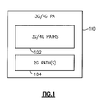
- Figure 1 shows that in some implementations, the present disclosure relates to a 3G/4G front-end architecture 100 that can accommodate one or more 2G amplification paths 104.
- Such an architecture can include a plurality of 3G/4G amplification paths 102 to provide, for example, MMMB functionalities.
- the 2G amplification path(s) 104 of Figure 1 can be configured to utilize existing 3G/4G linear transmit paths and PA stages that are designed, optimized, and appropriately-sized for 3G/4G performance (e.g., linearity and efficiency).
- 3G/4G performance e.g., linearity and efficiency.
- Various non-limiting examples of such 2G amplification path(s) are described herein in greater detail.
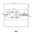
- Figure 2 shows an example of a 2G path 104 that can utilize components that are parts of a 3G/4G architecture 100.
- a first path that includes a PA 116 (PA1) and an output matching network 118 (OMN1) is a 3G/4G path.
- a second path that includes a PA 122 (PA2) and an output matching network 124 (OMN2) is a 3G/4G path.
- first and second 3G/4G paths are described in an example context of low band (LB) and very low band (VLB) paths.
- LB low band
- VLB very low band
- the 2G path 104 can include an input 110 configured to receive a 2G signal (e.g., Low Band GSM850 or EGSM900).
- a 2G signal e.g., Low Band GSM850 or EGSM900
- Such a signal can be divided by a splitter 112 into the first path associated with PA1 and the second path associated with PA2.
- the first path is shown to include a phase shifting circuit 114 before PA1, and the output matching network OMN1 after PA1.
- the second path is shown to include the output matching network OMN2 after PA2.
- the two paths are shown to be combined by a Wilkinson combiner 120 so as to yield an output 128 for the amplified 2G signal.
- Figure 3 shows an example of the Wilkinson combiner 120 of Figure 2 .
- First and second nodes 130, 132 can be connected to the outputs of OMN1 and OMN2, respectively, of Figure 2 .
- Such two nodes (130, 132) are shown to be resistively coupled through resistance R1.
- the first node 130 is shown to be coupled to ground through capacitance C1
- the second node 132 is shown to be coupled to ground through capacitance C2.
- Inductances L1 and L2 in series with each other and collectively parallel with R1 are shown to couple the first and second nodes 130, 132, such that the output 128 is at a node between L1 and L2.
- the output node 128 is shown to be coupled to ground through capacitance C3.
- the splitter 112 e.g., one or more switches
- the splitter 112 can be configured so that a given 2G signal is routed to the first path only, to the second path only, or to both of the first and second paths.
- Table 1 lists examples of saturated power level (Psat) performance that can be obtained or expected for the configuration of Figures 2 and 3 (with or without the Wilkinson combiner), when a 2G signal (824 MHz or 915 MHz) is amplified.
- the lossless Wilkinson combiner 120 in Figure 3
- the foregoing design that utilizes a Wilkinson combiner can include at least four SMT components, a resistor having high power rating, and two extra switch arms (e.g., to split the incoming 2G signal).
- Figure 4 shows an example of a 2G path 104 that can utilize components that are parts of a 3G/4G architecture 100.
- an additional shared throw can be implemented on an existing post-PA band-select switch to allow two low band 3G/4G amplifiers to be simultaneously connected to a common output pole of the post-PA band-select switch. From such an output pole, an impedance transformation network can be provided to optimally combine the outputs of the two PAs, to thereby reach a larger output power specification typically associated with 2G low bands.
- the post-PA band select switch can effectively isolate the foregoing combiner network from other 3G/4G optimized PAs and related paths; accordingly, there is little or no impact on the performance of various 3G/4G operations.
- a first path that includes a PA 156 (PA1) and an output matching network 158 (OMN1) is a 3G/4G path.
- a second path that includes a PA 162 (PA2) and an output matching network 164 (OMN2) is a 3G/4G path.
- first and second 3G/4G paths are described in an example context of low band (LB) and very low band (VLB) paths.
- LB low band
- VLB very low band
- the 2G path 104 can include an input 150 configured to receive a 2G signal (e.g., Low Band GSM850 or EGSM900).
- a 2G signal e.g., Low Band GSM850 or EGSM900
- Such a signal can be divided by a splitter 152 into the first path associated with PA1 and the second path associated with PA2.
- the first path is shown to include a phase shifting circuit 154 before PA1, and the output matching network OMN1 after PA1.
- the second path is shown to include the output matching network OMN2 after PA2.
- the two paths are shown to be combined by a combiner 160, and the combined path is shown to include an impedance transformer 166 configured to yield an output 168 for the amplified 2G signal.
- Figure 5A shows a more specific example of the 3G/4G architecture 100 of Figure 4 .
- the splitter 152, the phase shifting circuit 154, the OMNs 158, 164, and the combiner 160 of Figure 4 are generally indicated with the same reference numbers.
- Figure 5A shows that in some embodiments, the splitter 152 can include first and second switches S1, S2 connected to a common input 150.
- the first switch S1 is shown to be in series with the phase shifting circuit 154 and the first PA 156 (PA1).
- the second switch S2 is shown to be in series with the second PA 162 (PA2).
- operations of the first and second switches S1, S2 can route an incoming 2G signal to the first PA (PA1) only (e.g., S1 closed, S2 open), to the second PA only (e.g., S1 open, S2 closed), or to both of the first and second PAs (PA1 and PA2) (e.g., S1 closed, S2 closed).
- S1 and S2 are both closed; accordingly, the incoming 2G signal is routed to both of the first and second PAs (PA1 and PA2).
- the phase shifting circuit 154 can include an inductance L1, with each end of L1 being coupled to ground through a capacitance (C1 or C1').
- Such an example configuration of the phase shifting circuit 154 can provide a phase shift of approximately 60 degrees for the low band 2G signal. It will be understood that the phase shifting circuit 154 can be configured to provide a different amount of phase shift, and/or to accommodate a different frequency signal.
- each of the first and second PAs can include one or more stages.
- each PA can include a driver stage and an output stage.
- each PA in Figure 5A can be provided with a supply voltage VCC1 for the driver stage, and a supply voltage VCC2 for the output stage.
- FIG. 5A shows that in some embodiments, both of the OMNs 158, 164 can be implemented as an integrated passive device (IPD) 192.
- IPD integrated passive device
- Such an IPD can also include matching networks for other 3G/4G PAs.
- Figure 5A shows that in some embodiments, the phase shifting circuit 154, the PAs (PA1, PA2), and the IPD 192 with the OMNs 158, 164 can be considered to be functionally a PA block 190.
- a functional block can be implemented in one or more die.
- the IPD 192 and a die with the PAs can be stacked to reduce lateral footprint size.
- the IPD 192 and a band selection switch 194 of Figure 5A can be stacked. As one can see, a number of different configurations can be implemented.
- Figure 5A shows that in some embodiments, the combiner 160 of Figure 4 can be implemented in the band selection switch 194.
- the outputs of the OMNs 158, 164 for the first and second paths are shown to be connected to their respective poles that may or may not already exist in the band selection switch 194 for 3G/4G operations.
- Various throws in the band selection switch 194 are shown to be connected to their respective duplexers 198.
- An additional throw 196 can be provided in the band selection switch 194, and such a throw can be connected to an impedance transformer 166 as described herein.
- the band selection switch 194 can be operated to form connections between the output of the first OMN 158 and the throw 196, and between the output of the first OMN 164 and the throw 196, to thereby provide a combined path that includes the impedance transformer 166 and the output 168.
- the duplexers 198 are depicted as including channels for example bands B8, B26, B20, B17, B27, B13, B28, B12, and B28B/B29. It will be understood that more or less numbers of bands, and/or other bands, can be implemented and switched through the band selection switch 194.
- Figure 5B shows an alternate design for the example of Figure 5A . More particularly, the example of Figure 5B is shown to include a combiner 160 that is different than the combiner of Figure 5A .
- the splitter 152, the PA block 190, and the duplexers 198 of Figure 5B can be similar to those of Figure 5A .
- the outputs of the OMNs 158, 164 for the first and second paths are shown to be connected to their respective poles that may or may not already exist in the band selection switch 194 for 3G/4G operations, similar to the example of Figure 5A .
- the band selection switch 194 of Figure 5B there are two throws 193a, 193b that can be connected to such two poles.
- the throw 193a is shown to be connected to an input of a first matching network 195a
- the throw 193b is shown to be connected to an input of a second matching network 195b.
- Outputs of the first and second matching networks 195a, 195b are shown to be connected to a common node 197.
- the combiner in the example of Figure 5B can include the foregoing paths between the OMNs 158, 164 and the common node 197.
- an impedance transformer 166 is shown to be implemented between the common node 197 and the output 168.
- Such an impedance transformer may or may not be the same as the example 25ohm-to-50ohm transformer of Figure 5A .
- FIG 6 shows an example circuit that can be implemented as the impedance transformer 166 of Figures 5A and 5B .
- Such a circuit can include inductances L4 and L5 connected in series between the common throw 196 of the band selection switch 194 and the output 168 of Figure 5A , and between the common node 197 and the output 168 of Figure 5B .
- the impedance transformer circuit 166 is shown to further include capacitance C4 that couples a node between L4 and L5 to ground, and capacitance C5 that couples the output node 128 to ground.
- the impedance transformer 166 is depicted as providing 25 ohm (on the common node (196) side) to 50 ohm (on the output (168) side) transformation.
- values of L4, L5, C4 and C5 in Figure 6 can be as follows.
- L4 can be approximately 3.74 nH
- L5 can be approximately 7.91 nH
- C4 can be approximately 6.33 pF
- C5 can be approximately 2.99 pF.
- L4 can be approximately 3.6 nH
- L5 can be approximately 7.7 nH
- C4 can be approximately 6.2 pF
- C5 can be approximately 3 pF.
- Such an example configuration of the impedance transformer 166 can enhance output power for the low band 2G signal processed as described herein. It will be understood that the impedance transformer 166 can be configured to provide different transformations, and/or to accommodate a different frequency signals.
- the impedance transformer 166 of Figures 4-6 may be implemented using a number of other techniques, including, for example, transmission lines, lumped element reactive transformation, and transformer based on coupled coils of various winding relationships to achieve different impedance transformations.
- Required or desired phase and amplitude relationships between the two PA paths can be achieved through, for example, application of phase shifting and amplitude adjustment at the input of one or the other, or combinations of the stages relative to the other in order to avoid output losses.
- the phase and amplitude adjustment networks can also be implemented at the output side of PA(s), with some loss penalty.
- Figure 7A shows a plot of S11 parameter (reflection coefficient) as a function of frequency, demonstrating broadband property.
- Figure 7B shows a plot of insertion loss as a function of frequency, demonstrating a reasonable insertion loss of about 0.3 dB.
- Figures 8-12 show power amplification gain plots as a function of output power for the various example configurations described herein. More particularly, Figure 8 is for the example of Figure 2 , with VLB path only, after the OMN (124); Figure 9 is for the example of Figure 2 , with LB path only (no phase shift), after the OMN (118); Figure 10 is for the example of Figure 2 , with VLB and LB (290 degree phase shift), after the Wilkinson combiner (120); Figure 11 is for the example of Figure 5A , with VLB and LB (60 degree phase shift), after the impedance transformer (166) (with 0.3 dB loss), with VCC (e.g., VCC2 in Figure 5A ) at 3.4V; and Figure 12 is for the example of Figure 5A , with VLB and LB (60 degree phase shift), after the impedance transformer (166) (with 0.3 dB loss), with VCC increased to 3.8V.
- Figure 8 is for the example of Figure 2 , with VLB path only,
- Table 2 includes a summary of such Psat values for the plots shown in Figures 8-12 . It is noted that the first four rows of Table 2 are the same as Table 1. It is also noted that for the purpose of description, the example configuration of Figure 5A is sometimes referred to herein as a load-sharing configuration when both of the first and second paths (associated with PA1 and PA2) are active.
- the load-sharing configuration of Figure 5A provides good performance similar to the level of performance provided by the lossless Wilkinson-combiner example of Figure 2 .
- the load-sharing configuration of Figure 5A can be implemented with much less number of extra components. Accordingly, the load-sharing configuration of Figure 5A can provide advantageous savings in cost and space.
- one or more features of the present disclosure can advantageously allow, among others, elimination of one or more dedicated 2G power amplifiers and related RF paths through efficient combination of existing paths. As described herein, such existing paths can maintain their optimal performance in the linear 3G/4G modes, as originally designed.
- VCC power supply VCC
- a change in power supply VCC can affect amplification performance for 2G signals.
- such an adjustment in VCC may adversely affect the 3G/4G efficiency/linearity performance.
- trade-off in performance may be acceptable, especially when one considers that processing of 2G signals as described herein can have minimal impact on area and cost for the 3G/4G paths.
- one or more features of the present disclosure can also be implemented in systems involving more than two amplification paths.
- one or more features of the present disclosure can be utilized to extend the power combining advantage to much larger power levels of a combined PA using three or more PA paths.
- Figure 13 shows a process 300 that can be implemented to process 2G signals in a 3G/4G PA engine.
- a 2G signal can be provided to an input of a 3G/4G power amplifier (PA).
- PA power amplifier
- the 2G signal can be split into first and second paths.
- a phase shift can be introduced to the 2G signal in the first path.
- the 2G signal in each of the first and second paths can be amplified.
- each of the amplified 2G signals can be impedance matched.
- the amplified 2G signals from the first and second paths can be combined.
- impedance transformation can be performed on the combined 2G signal.
- impedance transformed 2G signal can be routed to an antenna for transmission.
- one or more features associated with 2G amplification using 3G4G path combination as described herein can be implemented in a PA system having an interface compatible with inputs that are separated by mode or frequency. Additional details concerning such a PA system are described in U.S. Provisional Application No. 62/038,323 filed August 17, 2014 , entitled POWER AMPLIFIER INTERFACE COMPATIBLE WITH INPUTS SEPARATED BY MODE OR FREQUENCY, and its corresponding U.S. Application entitled POWER AMPLIFIER INTERFACE COMPATIBLE WITH INPUTS SEPARATED BY MODE OR FREQUENCY, each of which is expressly incorporated by reference in its entirely, and which is to be considered part of the specification of the present application.
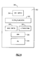
- FIG 14 shows that in some embodiments, some of all of the 3G/4G architecture as described herein can be implemented as a packaged module.
- a front-end module (FEM) 350 can include a packaging substrate 352 configured to receive a plurality of components.
- Such components include, for example, a PA die 354 having a plurality of amplification paths to facilitate 3G/4G MMMB operations.
- a PA die 354 having a plurality of amplification paths to facilitate 3G/4G MMMB operations.
- 2G PAs are traditionally implemented on such a die
- some or all of such 2G PAs can be eliminated, and 2G functionalities can be achieved, by utilizing one or more of the techniques described herein. Accordingly, such a PA die size and cost can be reduced.
- the example FEM 350 is shown to further include a band selection switch 358. As described herein, such a switch can be configured to provide combining functionality for 2G signals routed to two or more amplification paths.
- the example FEM 350 is shown to further include an impedance transformer 360. As described herein, such a transformer can be configured to improve the output power for transmission of 2G signals processed through a 3G/4G engine.
- the example FEM 350 is shown to further include an assembly of filters and duplexers 362.
- filters and duplexers can provide filtering and duplexing functionalities for 3G/4G signals, as well as 2G signals processed through the 3G/4G engine.
- the example FEM 350 is shown to further include an antenna switch 364.
- Such a switch can be configured to route various 3G/4G signals, as well as 2G signals being transmitted.
- a device and/or a circuit having one or more features described herein can be included in an RF device such as a wireless device.
- a wireless device such as a wireless device.
- Such a device and/or a circuit can be implemented directly in the wireless device, in a modular form as described herein, or in some combination thereof.
- such a wireless device can include, for example, a cellular phone, a smart-phone, a hand-held wireless device with or without phone functionality, a wireless tablet, etc.
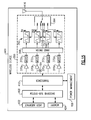
- FIG. 15 depicts an example wireless device 400 having one or more advantageous features described herein.
- a module having one or more features as described herein, such a module can be generally depicted by a dashed box 350, and can be implemented as a front-end module (FEM) such as a FEM-including-duplexer (FEMiD).
- FEM front-end module
- FEMiD FEM-including-duplexer
- PAs 370 can receive their respective RF signals from a transceiver 410 that can be configured and operated to generate RF signals to be amplified and transmitted, and to process received signals.
- the transceiver 410 is shown to interact with a baseband sub-system 408 that is configured to provide conversion between data and/or voice signals suitable for a user and RF signals suitable for the transceiver 410.
- the transceiver 410 is also shown to be connected to a power management component 406 that is configured to manage power for the operation of the wireless device. Such power management can also control operations of the baseband sub-system 408 and the module 350.
- the baseband sub-system 408 is shown to be connected to a user interface 402 to facilitate various input and output of voice and/or data provided to and received from the user.
- the baseband sub-system 408 can also be connected to a memory 404 that is configured to store data and/or instructions to facilitate the operation of the wireless device, and/or to provide storage of information for the user.
- outputs of the PAs 370 are shown to be matched (via respective match circuits 372) and routed to an antenna 416 through a band selection switch 358, their respective duplexers 362 and an antenna switch 364.
- each duplexer 362 can allow transmit and receive operations to be performed simultaneously using a common antenna (e.g., 416).
- received signals are shown to be routed to "Rx" paths (not shown) that can include, for example, a low-noise amplifier (LNA).
- LNA low-noise amplifier
- one or more phase shifting circuits 154 can be implemented at input(s) of the PA(s) 370 to facilitate processing of 2G signals as described herein.
- the band selection switch 358 can be configured to provide combining functionality for two or more amplification paths as described herein.
- an impedance transformer 166 can be implemented at a combined path from the band selection switch 358 to facilitate processing of 2G signals as described herein. In some embodiments, such an impedance transformer can be routed directly to the antenna switch 364 so as to allow transmission through the antenna 416.
- a wireless device does not need to be a multi-band device.
- a wireless device can include additional antennas such as diversity antenna, and additional connectivity features such as Wi-Fi, Bluetooth, and GPS.
Landscapes
- Engineering & Computer Science (AREA)
- Power Engineering (AREA)
- Computer Networks & Wireless Communication (AREA)
- Signal Processing (AREA)
- Microelectronics & Electronic Packaging (AREA)
- Amplifiers (AREA)
- Transceivers (AREA)
- Transmitters (AREA)
Abstract
Description
- This application claims priority to
U.S. Provisional Application Nos. 62/038,322 filed August 17, 2014 62/038,323 filed August 17, 2014 - The present disclosure relates to 2G amplification using 3G/4G path combination.
- Many wireless devices are configured to support current telecommunication standards, as well as one or more older standards. For example, many 3G/4G devices are configured to support 2G cellular standard.
- According to some implementations, the present disclosure relates to a front-end architecture that includes a first amplification path and a second amplification path, with each being configured to amplify a 3G/4G signal, and the first amplification path including a phase shifting circuit. The front-end architecture further includes a splitter configured to receive a 2G signal and split the 2G signal into the first and second amplification paths, and a combiner configured to combine amplified 2G signals from the first and second amplification paths into a common output path. The front-end architecture further includes an impedance transformer implemented along the common output path to provide a desired impedance for the combined 2G signal.
- In some embodiments, the splitter can include a first switch between a common input and the first amplification path, and a second switch between the common input and the second amplification path. Each of the first and second switches can be closed when the 2G signal is received and split into the first and second amplification paths.
- In some embodiments, each of the first and second amplification paths can include a power amplifier (PA). The phase shifting circuit can be on the input side of the PA. The phase shifting circuit can include an inductance and a capacitance that couples each end of the inductance to ground.
- In some embodiments, each of the first and second amplification paths can include an output matching network (OMN). In some embodiments, both OMNs can be implemented as an integrated passive device (IPD). In some embodiments, each OMN can include an inductance and a capacitance that couples the output side of the inductance to ground.
- In some embodiments, the combiner can be part of a band selection switch on the output side of the PAs of the first and second amplification paths. The band selection switch can include a pole connected to each of the first and second amplification paths. The pole connected to the corresponding amplification path can be an existing pole for 3G/4G operation. The band selection switch can further include a throw connected to the impedance transformer. The band selection switch can be configured to connect each pole associated with the corresponding amplification path to the throw associated with the impedance transformer.
- In some embodiments, the impedance transformer can include a first inductance and a second inductance connected in series, a first capacitance that couples a node between the first and second inductances to ground, and a second capacitance that couples the output side of the second inductance to ground.
- In some embodiments, the first and second amplification paths can be configured to amplify low band (LB) and very low band (VLB) 3G/4G signals, respectively. The 2G signal can have a frequency in, for example, a range between 820 MHz and 920 MHz. The 2G signal can include a signal in, for example, a GSM850 band or an EGSM900 band.
- In some teachings, the present disclosure relates to a method for amplifying a 2G signal. The method includes splitting the 2G signal to yield a split signal into each of a first amplification path and a second amplification path, with each of the first and second amplification paths being configured to amplify a 3G/4G signal. The method further includes phase shifting the split signal in the first amplification path, and amplifying the split signal in each of the first and second amplification paths. The method further includes combining the amplified signals from the first and second amplification paths to yield a combined signal, and providing a desired impedance transformation for the combined signal.
- In some embodiments, the amplifying can include providing a supply voltage to a power amplifier (PA) in each of the first and second amplification paths. In some embodiments, the method can further include adjusting the supply voltage to increase the saturated power level (Psat) of the amplified 2G signal. The adjusting can include increasing the supply voltage.
- In a number of implementations, the present disclosure relates to a front-end module (FEM) that includes a packaging substrate configured to receive a plurality of components, and a power amplifier (PA) die mounted on the packaging substrate. The PA die includes a first amplification path and a second amplification path, with each being configured to amplify a 3G/4G signal, and the first amplification path including a phase shifting circuit. The FEM further includes a splitter configured to receive a 2G signal and split the 2G signal into the first and second amplification paths, and a band selection switch configured to combine amplified 2G signals from the first and second amplification paths into a common output path. The FEM further includes an impedance transformer implemented along the common output path to provide a desired impedance for the combined 2G signal.
- In some embodiments, the PA die or the FEM can be substantially free of a 2G amplification path for amplifying the 2G signal. In some embodiments, the FEM can be substantially free of a 2G matching network for associated with the 2G amplification path.
- According to some teachings, the present disclosure relates to a wireless device that includes a transceiver configured to generate a radio-frequency (RF) signal, and a front-end architecture in communication with the transceiver. The front-end architecture is configured to process 3G/4G signals, and includes a first amplification path and a second amplification path, with each being configured to amplify a 3G/4G signal, and the first amplification path including a phase shifting circuit. The front-end architecture further includes a splitter configured to receive a 2G signal and split the 2G signal into the first and second amplification paths, and a combiner configured to combine amplified 2G signals from the first and second amplification paths into a common output path. The front-end architecture further includes an impedance transformer implemented along the common output path to provide a desired impedance for the combined 2G signal. The wireless device further includes an antenna in communication with the front-end architecture, and configured to facilitate transmission of the amplified 2G signal.
- In some embodiments, the wireless device can be a cellular phone. In some embodiments, the cellular phone can be a 3G/4G device having 2G capability. In some embodiments, the cellular phone can be capable of operating in a GSM850 band or an EGSM900 band.
- For purposes of summarizing the disclosure, certain aspects, advantages and novel features of the inventions have been described herein. It is to be understood that not necessarily all such advantages may be achieved in accordance with any particular embodiment of the invention. Thus, the invention may be embodied or carried out in a manner that achieves or optimizes one advantage or group of advantages as taught herein without necessarily achieving other advantages as may be taught or suggested herein.
-
-
Figure 1 depicts a 3G/4G front-end architecture that can accommodate one or more 2G amplification paths. -
Figure 2 shows an example of a 2G path that can utilize components that are parts of a 3G/4G architecture. -
Figure 3 shows an example of a combiner that can be utilized in the example ofFigure 2 . -
Figure 4 shows another example of a 2G path that can utilize components that are parts of a 3G/4G architecture. -
Figure 5A shows a more specific example of the 3G/4G architecture ofFigure 4 . -
Figure 5B shows an alternate design for the example ofFigure 5A . -
Figure 6 shows an example circuit that can be implemented as an impedance transformer in the examples ofFigures 5A and5B . -
Figures 7A and 7B show examples of performance that can be obtained or expected with use of the impedance transformer ofFigures 5 and6 . -
Figure 8 show power amplification gain plots as a function of output power for the example ofFigure 2 in a configuration. -
Figure 9 show power amplification gain plots as a function of output power for the example ofFigure 2 in another configuration. -
Figure 10 show power amplification gain plots as a function of output power for the example ofFigure 2 in yet another configuration. -
Figure 11 show power amplification gain plots as a function of output power for the example ofFigure 5A in a configuration. -
Figure 12 show power amplification gain plots as a function of output power for the example ofFigure 5A in another configuration. -
Figure 13 shows a process that can be implemented to process 2G signals in a 3G/4G power amplifier (PA) engine. -
Figure 14 shows that in some embodiments, some of all of the 3G/4G architecture as described herein can be implemented as a packaged module. -
Figure 15 depicts an example wireless device having one or more advantageous features described herein. - The headings provided herein, if any, are for convenience only and do not necessarily affect the scope or meaning of the claimed invention.
- Support for 2G configurations such as GMSK/8PSK transmit radio-frequency (RF) paths in the front-end of multi-mode multi-band (MMMB) cellular devices has conventionally required dedicated power amplifier (PA) RF blocks in order to address efficiency and target output power requirements. Low band (LB) 2G (e.g., Low Band GSM850 and EGSM900) is especially challenging, as it typically requires 33dBm output power at a cellular antenna, whereas a peak power of a typical linear 3G/4G power amplifier (PA) may be closer to 27dBm. It is also noted that design factors such as active die area, output match and connectivity can have substantive impact to area and/or cost of such front-ends.
- In some applications, 2G support can be achieved through the use of dedicated 2G PAs and radio-frequency (RF) paths with some impact to cost and/or size. For example, an overall size associated with 2G PA transistors can be more than double the size of 3G PA transistors.
- In other applications, use of electrical re-sizing of 3G/4G linear path can be utilized. However, such a technique typically involves adjustment of lossy DC-DC converter supply voltage and/or load impedance switching that can result in poor DC consumption performance and negative impact on the 3G/4G linear path efficiency and/or linearity.
-
Figure 1 shows that in some implementations, the present disclosure relates to a 3G/4G front-end architecture 100 that can accommodate one or more2G amplification paths 104. Such an architecture can include a plurality of 3G/4G amplification paths 102 to provide, for example, MMMB functionalities. - In some embodiment, and as described herein, the 2G amplification path(s) 104 of
Figure 1 can be configured to utilize existing 3G/4G linear transmit paths and PA stages that are designed, optimized, and appropriately-sized for 3G/4G performance (e.g., linearity and efficiency). Various non-limiting examples of such 2G amplification path(s) are described herein in greater detail. -
Figure 2 shows an example of a2G path 104 that can utilize components that are parts of a 3G/4G architecture 100. In the example ofFigure 2 , a first path that includes a PA 116 (PA1) and an output matching network 118 (OMN1) is a 3G/4G path. Similarly, a second path that includes a PA 122 (PA2) and an output matching network 124 (OMN2) is a 3G/4G path. In various examples herein, such first and second 3G/4G paths are described in an example context of low band (LB) and very low band (VLB) paths. However, it will be understood that one or more features of the present disclosure can also be implemented with path(s) associated with other frequency bands. - In the example of
Figure 2 , the2G path 104 can include aninput 110 configured to receive a 2G signal (e.g., Low Band GSM850 or EGSM900). Such a signal can be divided by asplitter 112 into the first path associated with PA1 and the second path associated with PA2. The first path is shown to include aphase shifting circuit 114 before PA1, and the output matching network OMN1 after PA1. The second path is shown to include the output matching network OMN2 after PA2. The two paths are shown to be combined by aWilkinson combiner 120 so as to yield anoutput 128 for the amplified 2G signal. -
Figure 3 shows an example of theWilkinson combiner 120 ofFigure 2 . First andsecond nodes Figure 2 . Such two nodes (130, 132) are shown to be resistively coupled through resistance R1. Thefirst node 130 is shown to be coupled to ground through capacitance C1, and thesecond node 132 is shown to be coupled to ground through capacitance C2. Inductances L1 and L2 in series with each other and collectively parallel with R1 are shown to couple the first andsecond nodes output 128 is at a node between L1 and L2. Theoutput node 128 is shown to be coupled to ground through capacitance C3. - It is noted that in the example of
Figure 2 , the splitter 112 (e.g., one or more switches) can be configured so that a given 2G signal is routed to the first path only, to the second path only, or to both of the first and second paths. With such routing options, and in the example context of the first and second paths being 3G/4G LB and VLB paths, Table 1 lists examples of saturated power level (Psat) performance that can be obtained or expected for the configuration ofFigures 2 and 3 (with or without the Wilkinson combiner), when a 2G signal (824 MHz or 915 MHz) is amplified.Table 1 Path(s) used Psat (dBm) at 824 MHz Psat (dBm) at 915 MHz Phase compensation (degrees) VLB only 31.9 32.7 N/A LB only 30.8 31.3 N/A VLB and LB (calculated) 34.4 35.1 N/A VLB and LB with lossless Wilkinson combiner 34.8 34.9 Ideal phase shift of 290 degrees at the input of LB - Following observations can be made in reference to Table 1. The "VLB only" case showed higher Psat than the "LB only" case in the simulation bench due to lower loadline. The lossless Wilkinson combiner (120 in
Figure 3 ) was modeled with ideal resistor, inductors and capacitors (R1 = 100 ohms, C1 = C2 = 2.6 pF, L1 = L2 = 13 nH, C3 = 5.1 pF). Accordingly, in some embodiments, the foregoing design that utilizes a Wilkinson combiner can include at least four SMT components, a resistor having high power rating, and two extra switch arms (e.g., to split the incoming 2G signal). -
Figure 4 shows an example of a2G path 104 that can utilize components that are parts of a 3G/4G architecture 100. In the example ofFigure 4 , an additional shared throw can be implemented on an existing post-PA band-select switch to allow twolow band 3G/4G amplifiers to be simultaneously connected to a common output pole of the post-PA band-select switch. From such an output pole, an impedance transformation network can be provided to optimally combine the outputs of the two PAs, to thereby reach a larger output power specification typically associated with 2G low bands. Further, the post-PA band select switch can effectively isolate the foregoing combiner network from other 3G/4G optimized PAs and related paths; accordingly, there is little or no impact on the performance of various 3G/4G operations. - Referring to the example of
Figure 4 , a first path that includes a PA 156 (PA1) and an output matching network 158 (OMN1) is a 3G/4G path. Similarly, a second path that includes a PA 162 (PA2) and an output matching network 164 (OMN2) is a 3G/4G path. In various examples herein, such first and second 3G/4G paths are described in an example context of low band (LB) and very low band (VLB) paths. However, it will be understood that one or more features of the present disclosure can also be implemented with path(s) associated with other frequency bands. - In the example of
Figure 4 , the2G path 104 can include aninput 150 configured to receive a 2G signal (e.g., Low Band GSM850 or EGSM900). Such a signal can be divided by asplitter 152 into the first path associated with PA1 and the second path associated with PA2. The first path is shown to include aphase shifting circuit 154 before PA1, and the output matching network OMN1 after PA1. The second path is shown to include the output matching network OMN2 after PA2. The two paths are shown to be combined by acombiner 160, and the combined path is shown to include animpedance transformer 166 configured to yield anoutput 168 for the amplified 2G signal. -
Figure 5A shows a more specific example of the 3G/4G architecture 100 ofFigure 4 . InFigure 5A , thesplitter 152, thephase shifting circuit 154, theOMNs combiner 160 ofFigure 4 are generally indicated with the same reference numbers. -
Figure 5A shows that in some embodiments, thesplitter 152 can include first and second switches S1, S2 connected to acommon input 150. The first switch S1 is shown to be in series with thephase shifting circuit 154 and the first PA 156 (PA1). The second switch S2 is shown to be in series with the second PA 162 (PA2). Accordingly, operations of the first and second switches S1, S2 can route an incoming 2G signal to the first PA (PA1) only (e.g., S1 closed, S2 open), to the second PA only (e.g., S1 open, S2 closed), or to both of the first and second PAs (PA1 and PA2) (e.g., S1 closed, S2 closed). In the example shown inFigure 5A , S1 and S2 are both closed; accordingly, the incoming 2G signal is routed to both of the first and second PAs (PA1 and PA2). -
Figure 5A shows that in some embodiments, thephase shifting circuit 154 can include an inductance L1, with each end of L1 being coupled to ground through a capacitance (C1 or C1'). In the context of the first and second PAs (PA1 and PA2) being LB and VLB PAs, and the 2G signal being a low band signal (e.g., 824 MHz or 915 MHz), example values of L1, C1 and C1' can be as follows: L1 = 7.9 nH, C1 = C1' = 2.1 pF. Such an example configuration of thephase shifting circuit 154 can provide a phase shift of approximately 60 degrees for thelow band 2G signal. It will be understood that thephase shifting circuit 154 can be configured to provide a different amount of phase shift, and/or to accommodate a different frequency signal. -
Figure 5A shows that in some embodiments, each of the first and second PAs (PA1 and PA2) can include one or more stages. For example, each PA can include a driver stage and an output stage. In such a configuration, each PA inFigure 5A can be provided with a supply voltage VCC1 for the driver stage, and a supply voltage VCC2 for the output stage. -
Figure 5A shows that in some embodiments, both of theOMNs -
Figure 5A shows that in some embodiments, thephase shifting circuit 154, the PAs (PA1, PA2), and theIPD 192 with theOMNs PA block 190. Such a functional block can be implemented in one or more die. For example, theIPD 192 and a die with the PAs can be stacked to reduce lateral footprint size. In another example, theIPD 192 and aband selection switch 194 ofFigure 5A can be stacked. As one can see, a number of different configurations can be implemented. -
Figure 5A shows that in some embodiments, thecombiner 160 ofFigure 4 can be implemented in theband selection switch 194. For example, the outputs of theOMNs band selection switch 194 for 3G/4G operations. Various throws in theband selection switch 194 are shown to be connected to theirrespective duplexers 198. Anadditional throw 196 can be provided in theband selection switch 194, and such a throw can be connected to animpedance transformer 166 as described herein. Accordingly, theband selection switch 194 can be operated to form connections between the output of thefirst OMN 158 and thethrow 196, and between the output of thefirst OMN 164 and thethrow 196, to thereby provide a combined path that includes theimpedance transformer 166 and theoutput 168. - In the example of
Figure 5A , theduplexers 198 are depicted as including channels for example bands B8, B26, B20, B17, B27, B13, B28, B12, and B28B/B29. It will be understood that more or less numbers of bands, and/or other bands, can be implemented and switched through theband selection switch 194. -
Figure 5B shows an alternate design for the example ofFigure 5A . More particularly, the example ofFigure 5B is shown to include acombiner 160 that is different than the combiner ofFigure 5A . For the purpose of description, thesplitter 152, thePA block 190, and theduplexers 198 ofFigure 5B can be similar to those ofFigure 5A . - In the example of
Figure 5B , the outputs of theOMNs band selection switch 194 for 3G/4G operations, similar to the example ofFigure 5A . In theband selection switch 194 ofFigure 5B , however, there are twothrows throw 193a is shown to be connected to an input of afirst matching network 195a, and thethrow 193b is shown to be connected to an input of asecond matching network 195b. Outputs of the first andsecond matching networks common node 197. Accordingly, the combiner in the example ofFigure 5B can include the foregoing paths between theOMNs common node 197. - In
Figure 5B , animpedance transformer 166 is shown to be implemented between thecommon node 197 and theoutput 168. Such an impedance transformer may or may not be the same as the example 25ohm-to-50ohm transformer ofFigure 5A . -
Figure 6 shows an example circuit that can be implemented as theimpedance transformer 166 ofFigures 5A and5B . Such a circuit can include inductances L4 and L5 connected in series between thecommon throw 196 of theband selection switch 194 and theoutput 168 ofFigure 5A , and between thecommon node 197 and theoutput 168 ofFigure 5B . Theimpedance transformer circuit 166 is shown to further include capacitance C4 that couples a node between L4 and L5 to ground, and capacitance C5 that couples theoutput node 128 to ground. - In
Figure 5A , theimpedance transformer 166 is depicted as providing 25 ohm (on the common node (196) side) to 50 ohm (on the output (168) side) transformation. In such an example context, values of L4, L5, C4 and C5 inFigure 6 can be as follows. In an ideal situation, L4 can be approximately 3.74 nH, L5 can be approximately 7.91 nH, C4 can be approximately 6.33 pF, and C5 can be approximately 2.99 pF. When implemented in SMT inductors and capacitors with Q factor of about 40, L4 can be approximately 3.6 nH, L5 can be approximately 7.7 nH, C4 can be approximately 6.2 pF, and C5 can be approximately 3 pF. Such an example configuration of theimpedance transformer 166 can enhance output power for thelow band 2G signal processed as described herein. It will be understood that theimpedance transformer 166 can be configured to provide different transformations, and/or to accommodate a different frequency signals. - It will be understood that the
impedance transformer 166 ofFigures 4-6 may be implemented using a number of other techniques, including, for example, transmission lines, lumped element reactive transformation, and transformer based on coupled coils of various winding relationships to achieve different impedance transformations. Required or desired phase and amplitude relationships between the two PA paths can be achieved through, for example, application of phase shifting and amplitude adjustment at the input of one or the other, or combinations of the stages relative to the other in order to avoid output losses. In some applications, the phase and amplitude adjustment networks can also be implemented at the output side of PA(s), with some loss penalty. -
Figures 7A and 7B show examples of performance that can be obtained or expected with use of theimpedance transformer 166 ofFigures 5 and6 , with the foregoing SMT implementations (e.g., with Q = 40).Figure 7A shows a plot of S11 parameter (reflection coefficient) as a function of frequency, demonstrating broadband property.Figure 7B shows a plot of insertion loss as a function of frequency, demonstrating a reasonable insertion loss of about 0.3 dB. -
Figures 8-12 show power amplification gain plots as a function of output power for the various example configurations described herein. More particularly,Figure 8 is for the example ofFigure 2 , with VLB path only, after the OMN (124);Figure 9 is for the example ofFigure 2 , with LB path only (no phase shift), after the OMN (118);Figure 10 is for the example ofFigure 2 , with VLB and LB (290 degree phase shift), after the Wilkinson combiner (120);Figure 11 is for the example ofFigure 5A , with VLB and LB (60 degree phase shift), after the impedance transformer (166) (with 0.3 dB loss), with VCC (e.g., VCC2 inFigure 5A ) at 3.4V; andFigure 12 is for the example ofFigure 5A , with VLB and LB (60 degree phase shift), after the impedance transformer (166) (with 0.3 dB loss), with VCC increased to 3.8V. From such plots, saturated power levels (Psat) can be obtained. Table 2 includes a summary of such Psat values for the plots shown inFigures 8-12 . It is noted that the first four rows of Table 2 are the same as Table 1. It is also noted that for the purpose of description, the example configuration ofFigure 5A is sometimes referred to herein as a load-sharing configuration when both of the first and second paths (associated with PA1 and PA2) are active.Table 2 Path(s) used Psat (dBm) at 824 MHz Psat (dBm) at 915 MHz Phase compensation (degrees) VLB only 31.9 32.7 N/A LB only 30.8 31.3 N/A VLB and LB (calculated) 34.4 35.1 N/A VLB and LB with lossless Wilkinson combiner 34.8 34.9 Ideal phase shift of 290 degrees at the input of LB Load-sharing (VLB and LB) with lossless impedance transformer, with ideal lumped elements in OMNs 34.8 35.2 Ideal transmission line phase shift of 60 degrees Load-sharing (VLB and LB) with lossy (0.3 dB) impedance transformer, with SMT model used for OMNs, VCC = 3.4V 34.5 34.9 Lumped C-L-C elements, phase shift of 60 degrees Load-sharing (VLB and LB) with lossy (0.3 dB) impedance transformer, with SMT model used for OMNs, VCC = 3.8V 35.5 35.9 Lumped C-L-C elements, phase shift of 60 degrees - Based on the performance summary of Table 2, one can see that the load-sharing configuration of
Figure 5A provides good performance similar to the level of performance provided by the lossless Wilkinson-combiner example ofFigure 2 . In contrast to the Wilkinson-combiner example ofFigure 2 in which a number of SMT components as well as high-power rated resistor are likely needed (as well as the extra space to accommodate such components), the load-sharing configuration ofFigure 5A can be implemented with much less number of extra components. Accordingly, the load-sharing configuration ofFigure 5A can provide advantageous savings in cost and space. - It is noted that one or more features of the present disclosure can advantageously allow, among others, elimination of one or more dedicated 2G power amplifiers and related RF paths through efficient combination of existing paths. As described herein, such existing paths can maintain their optimal performance in the linear 3G/4G modes, as originally designed.
- It is also noted that while various examples are described herein in the context of 3G/4G PAs, paths, etc., it will be understood that such PAs, paths, etc. can be configured for 3G operation, for 4G operation, or any combination thereof. It will also be understood that one or more features of the present disclosure can also be applied to configurations involving other generations of cellular standards used in the past, currently in use, to be defined and used in the future, or any combination thereof.
- It is also noted that in the example described in reference to
Figure 12 and Table 2, one can see that a change in power supply VCC can affect amplification performance for 2G signals. In some situations, such an adjustment in VCC may adversely affect the 3G/4G efficiency/linearity performance. Even in such situations, trade-off in performance may be acceptable, especially when one considers that processing of 2G signals as described herein can have minimal impact on area and cost for the 3G/4G paths. - It is also noted that while various examples are described herein in the context of two parallel amplification paths in 3G/4G architectures, one or more features of the present disclosure can also be implemented in other applications. For example, multiple PA combination methods for linearization, such as Doherty techniques where differing phase adjustment and amplitude balance are applied for backed-off efficiency advantage, can utilize one or more features of the present disclosure.
- It is also noted that while various examples are described in the context of two amplification paths, one or more features of the present disclosure can also be implemented in systems involving more than two amplification paths. For example, one or more features of the present disclosure can be utilized to extend the power combining advantage to much larger power levels of a combined PA using three or more PA paths.
-
Figure 13 shows aprocess 300 that can be implemented to process 2G signals in a 3G/4G PA engine. Inblock 302, a 2G signal can be provided to an input of a 3G/4G power amplifier (PA). Inblock 304, the 2G signal can be split into first and second paths. Inblock 306, a phase shift can be introduced to the 2G signal in the first path. Inblock 308, the 2G signal in each of the first and second paths can be amplified. Inblock 310, each of the amplified 2G signals can be impedance matched. Inblock 312, the amplified 2G signals from the first and second paths can be combined. Inblock 314, impedance transformation can be performed on the combined 2G signal. Inblock 316, impedance transformed 2G signal can be routed to an antenna for transmission. - In some embodiments, one or more features associated with 2G amplification using 3G4G path combination as described herein can be implemented in a PA system having an interface compatible with inputs that are separated by mode or frequency. Additional details concerning such a PA system are described in
U.S. Provisional Application No. 62/038,323 filed August 17, 2014 -
Figure 14 shows that in some embodiments, some of all of the 3G/4G architecture as described herein can be implemented as a packaged module. For example, a front-end module (FEM) 350 can include apackaging substrate 352 configured to receive a plurality of components. Such components include, for example, a PA die 354 having a plurality of amplification paths to facilitate 3G/4G MMMB operations. In situations where 2G PAs are traditionally implemented on such a die, some or all of such 2G PAs can be eliminated, and 2G functionalities can be achieved, by utilizing one or more of the techniques described herein. Accordingly, such a PA die size and cost can be reduced. In situations where 2G PAs are traditionally implemented on a separate die, such a die can be reduced in size or eliminated for similar reasons. Accordingly, the module size and cost can be reduced. It is further noted that one or more components that are traditionally mounted on thepackaging substrate 352 to facilitate 2G impedance matching and/or filtering functionalities can also be reduced or eliminated, thereby reducing the module size and cost. - The
example FEM 350 is shown to further include aband selection switch 358. As described herein, such a switch can be configured to provide combining functionality for 2G signals routed to two or more amplification paths. - The
example FEM 350 is shown to further include animpedance transformer 360. As described herein, such a transformer can be configured to improve the output power for transmission of 2G signals processed through a 3G/4G engine. - The
example FEM 350 is shown to further include an assembly of filters andduplexers 362. Such filters and duplexers can provide filtering and duplexing functionalities for 3G/4G signals, as well as 2G signals processed through the 3G/4G engine. - The
example FEM 350 is shown to further include anantenna switch 364. Such a switch can be configured to route various 3G/4G signals, as well as 2G signals being transmitted. - In some implementations, a device and/or a circuit having one or more features described herein can be included in an RF device such as a wireless device. Such a device and/or a circuit can be implemented directly in the wireless device, in a modular form as described herein, or in some combination thereof. In some embodiments, such a wireless device can include, for example, a cellular phone, a smart-phone, a hand-held wireless device with or without phone functionality, a wireless tablet, etc.
-
Figure 15 depicts anexample wireless device 400 having one or more advantageous features described herein. In the context of a module having one or more features as described herein, such a module can be generally depicted by a dashedbox 350, and can be implemented as a front-end module (FEM) such as a FEM-including-duplexer (FEMiD). - PAs 370 can receive their respective RF signals from a
transceiver 410 that can be configured and operated to generate RF signals to be amplified and transmitted, and to process received signals. Thetransceiver 410 is shown to interact with abaseband sub-system 408 that is configured to provide conversion between data and/or voice signals suitable for a user and RF signals suitable for thetransceiver 410. Thetransceiver 410 is also shown to be connected to apower management component 406 that is configured to manage power for the operation of the wireless device. Such power management can also control operations of thebaseband sub-system 408 and themodule 350. - The
baseband sub-system 408 is shown to be connected to auser interface 402 to facilitate various input and output of voice and/or data provided to and received from the user. Thebaseband sub-system 408 can also be connected to amemory 404 that is configured to store data and/or instructions to facilitate the operation of the wireless device, and/or to provide storage of information for the user. - In the
example wireless device 400, outputs of the PAs 370 are shown to be matched (via respective match circuits 372) and routed to anantenna 416 through aband selection switch 358, theirrespective duplexers 362 and anantenna switch 364. In some embodiments, eachduplexer 362 can allow transmit and receive operations to be performed simultaneously using a common antenna (e.g., 416). InFigure 15 , received signals are shown to be routed to "Rx" paths (not shown) that can include, for example, a low-noise amplifier (LNA). - In the
example wireless device 400, one or morephase shifting circuits 154 can be implemented at input(s) of the PA(s) 370 to facilitate processing of 2G signals as described herein. Further, theband selection switch 358 can be configured to provide combining functionality for two or more amplification paths as described herein. Further, animpedance transformer 166 can be implemented at a combined path from theband selection switch 358 to facilitate processing of 2G signals as described herein. In some embodiments, such an impedance transformer can be routed directly to theantenna switch 364 so as to allow transmission through theantenna 416. - A number of other wireless device configurations can utilize one or more features described herein. For example, a wireless device does not need to be a multi-band device. In another example, a wireless device can include additional antennas such as diversity antenna, and additional connectivity features such as Wi-Fi, Bluetooth, and GPS.
- Unless the context clearly requires otherwise, throughout the description and the claims, the words "comprise," "comprising," and the like are to be construed in an inclusive sense, as opposed to an exclusive or exhaustive sense; that is to say, in the sense of "including, but not limited to." The word "coupled", as generally used herein, refers to two or more elements that may be either directly connected, or connected by way of one or more intermediate elements. Additionally, the words "herein," "above," "below," and words of similar import, when used in this application, shall refer to this application as a whole and not to any particular portions of this application. Where the context permits, words in the above Description using the singular or plural number may also include the plural or singular number respectively. The word "or" in reference to a list of two or more items, that word covers all of the following interpretations of the word: any of the items in the list, all of the items in the list, and any combination of the items in the list.
- The above detailed description of embodiments of the invention is not intended to be exhaustive or to limit the invention to the precise form disclosed above. While specific embodiments of, and examples for, the invention are described above for illustrative purposes, various equivalent modifications are possible within the scope of the invention, as those skilled in the relevant art will recognize. For example, while processes or blocks are presented in a given order, alternative embodiments may perform routines having steps, or employ systems having blocks, in a different order, and some processes or blocks may be deleted, moved, added, subdivided, combined, and/or modified. Each of these processes or blocks may be implemented in a variety of different ways. Also, while processes or blocks are at times shown as being performed in series, these processes or blocks may instead be performed in parallel, or may be performed at different times.
- The teachings of the invention provided herein can be applied to other systems, not necessarily the system described above. The elements and acts of the various embodiments described above can be combined to provide further embodiments.
- While some embodiments of the inventions have been described, these embodiments have been presented by way of example only, and are not intended to limit the scope of the disclosure. Indeed, the novel methods and systems described herein may be embodied in a variety of other forms; furthermore, various omissions, substitutions and changes in the form of the methods and systems described herein may be made without departing from the spirit of the disclosure. The accompanying claims and their equivalents are intended to cover such forms or modifications as would fall within the scope and spirit of the disclosure.
Claims (15)
- A front-end architecture (100) comprising:a first amplification path and a second amplification path, each configured to amplify a 3G/4G signal, the first amplification path including a phase shifting circuit (154);a splitter (152) configured to receive a 2G signal and split the 2G signal into the first and second amplification paths;a combiner (160) configured to combine amplified 2G signals from the first and second amplification paths into a common output path (168); andan impedance transformer (166) implemented along the common output path (168) to provide a desired impedance for the combined 2G signal.
- The front-end architecture (100) of claim 1 wherein the splitter (152) includes a first switch (S1) between a common input and the first amplification path, and a second switch (S2) between the common input and the second amplification path.
- The front-end architecture (100) of claim 1 wherein each of the first and second amplification paths includes a power amplifier, PA, (156, 162).
- The front-end architecture (100) of claim 3 wherein the phase shifting circuit (154) includes an inductance (L1) and a capacitance (C1, C1') that couples each end of the inductance (L1) to ground.
- The front-end architecture (100) of claim 3 wherein each of the first and second amplification paths includes an output matching network, OMN, (158, 164).
- The front-end architecture (100) of claim 3 wherein the combiner (160) is part of a band selection switch (194) on the output side of the PAs of the first and second amplification paths.
- The front-end architecture (100) of claim 6 wherein the band selection switch (194) includes a pole connected to each of the first and second amplification paths.
- The front-end architecture (100) of claim 7 wherein the pole connected to the corresponding amplification path is an existing pole for 3G/4G operation.
- The front-end architecture (100) of claim 7 wherein the band selection switch (194) further includes a throw connected to the impedance transformer (166).
- The front-end architecture (100) of claim 9 wherein the band selection switch (194) is configured to connect each pole associated with the corresponding amplification path to the throw associated with the impedance transformer (166).
- The front-end architecture (100) of claim 1 wherein the impedance transformer (166) includes a first inductance (L4) and a second inductance (L5) connected in series, a first capacitance (C4) that couples a node between the first (L4) and second inductances (L5) to ground, and a second capacitance (C5) that couples the output side of the second inductance (L5) to ground.
- The front-end architecture (100) of claim 1 wherein the first and second amplification paths are configured to amplify low band, LB, and very low band, VLB, 3G/4G signals, respectively.
- A front-end module, FEM, (350) comprising the front-end architecture (100) of any of claims 1-12.
- A wireless device (400) comprising:a transceiver (410) configured to generate a radio-frequency, RF, signal;a front-end architecture (100) of any of claims 1-12; andan antenna (416) in communication with the front-end architecture (100), the antenna (416) configured to facilitate transmission of the combined 2G signal.
- A method (300) for amplifying a 2G signal, the method comprising:splitting (304) the 2G signal to yield a split signal into each of a first amplification path and a second amplification path, each of the first and second amplification paths configured to amplify a 3G/4G signal;phase shifting (306) the split signal in the first amplification path;amplifying (308) the split signal in each of the first and second amplification paths;combining (312) the amplified signals from the first and second amplification paths to yield a combined signal; andproviding (314) a desired impedance transformation for the combined signal.
Applications Claiming Priority (2)
| Application Number | Priority Date | Filing Date | Title |
|---|---|---|---|
| US201462038323P | 2014-08-17 | 2014-08-17 | |
| US201462038322P | 2014-08-17 | 2014-08-17 |
Publications (2)
| Publication Number | Publication Date |
|---|---|
| EP2988416A1 true EP2988416A1 (en) | 2016-02-24 |
| EP2988416B1 EP2988416B1 (en) | 2019-11-06 |
Family
ID=53871959
Family Applications (2)
| Application Number | Title | Priority Date | Filing Date |
|---|---|---|---|
| EP15181220.3A Active EP2988416B1 (en) | 2014-08-17 | 2015-08-17 | Circuits and methods for 2g amplification using 3g/4g linear path combination |
| EP15181239.3A Active EP2988417B1 (en) | 2014-08-17 | 2015-08-17 | Power amplifier interface compatible with inputs separated by mode or frequency |
Family Applications After (1)
| Application Number | Title | Priority Date | Filing Date |
|---|---|---|---|
| EP15181239.3A Active EP2988417B1 (en) | 2014-08-17 | 2015-08-17 | Power amplifier interface compatible with inputs separated by mode or frequency |
Country Status (5)
| Country | Link |
|---|---|
| US (3) | US20160190995A1 (en) |
| EP (2) | EP2988416B1 (en) |
| JP (4) | JP2016042700A (en) |
| CN (3) | CN111585534B (en) |
| TW (2) | TWI711270B (en) |
Cited By (5)
| Publication number | Priority date | Publication date | Assignee | Title |
|---|---|---|---|---|
| WO2017177214A1 (en) * | 2016-04-09 | 2017-10-12 | Skyworks Solutions, Inc. | Front-end architecture having switchable duplexer |
| CN109195118A (en) * | 2018-10-19 | 2019-01-11 | 江苏未来智慧信息科技有限公司 | Band PA One-to-All Broadcast communication device and communication means based on bluetooth |
| EP3319230B1 (en) * | 2016-11-03 | 2022-12-07 | NXP USA, Inc. | Amplifier architecture reconfiguration |
| CN115882791A (en) * | 2022-12-12 | 2023-03-31 | 深圳飞骧科技股份有限公司 | Voltage synthesis type Doherty power amplifier |
| CN120149776A (en) * | 2025-05-16 | 2025-06-13 | 深圳飞骧科技股份有限公司 | RF power division unit, RF power division module and RF receiving system |
Families Citing this family (34)
| Publication number | Priority date | Publication date | Assignee | Title |
|---|---|---|---|---|
| JP6616241B2 (en) * | 2015-05-22 | 2019-12-04 | スカイワークス ソリューションズ,インコーポレイテッド | Combined output matching network and filter with parallel function for power amplifier |
| JP6755298B2 (en) * | 2015-07-06 | 2020-09-16 | テレフオンアクチーボラゲット エルエム エリクソン(パブル) | Resource allocation for data transmission in wireless systems |
| JP2017103655A (en) | 2015-12-02 | 2017-06-08 | 株式会社村田製作所 | Power Amplifier Module |
| KR102468952B1 (en) | 2016-03-07 | 2022-11-22 | 삼성전자주식회사 | Electronic apparatus and method for transceiving signals |
| US9887673B2 (en) * | 2016-03-11 | 2018-02-06 | Intel Corporation | Ultra compact multi-band transmitter with robust AM-PM distortion self-suppression techniques |
| US9948350B2 (en) * | 2016-07-06 | 2018-04-17 | Qorvo Us, Inc. | Multi-mode radio frequency circuitry |
| JP2018050167A (en) | 2016-09-21 | 2018-03-29 | 株式会社村田製作所 | Power Amplifier Module |
| JP2018085560A (en) | 2016-11-21 | 2018-05-31 | 株式会社村田製作所 | Power Amplifier Module |
| US10469033B2 (en) | 2016-11-21 | 2019-11-05 | Murata Manufacturing Co., Ltd. | Power amplification module |
| US10148226B2 (en) | 2016-12-09 | 2018-12-04 | Murata Manufacturing Co., Ltd. | Bias circuit |
| JP2018098766A (en) | 2016-12-09 | 2018-06-21 | 株式会社村田製作所 | Bias circuit |
| EP3442120B1 (en) * | 2017-08-08 | 2021-02-03 | Rohde & Schwarz GmbH & Co. KG | Amplifier circuit and method |
| JP2019193115A (en) | 2018-04-25 | 2019-10-31 | 株式会社村田製作所 | High-frequency amplifier circuit, high-frequency front end circuit, and communication apparatus |
| CN108768434B (en) * | 2018-06-06 | 2021-02-12 | 维沃移动通信有限公司 | Radio frequency circuit, terminal and signal transmission control method |
| WO2019244757A1 (en) | 2018-06-19 | 2019-12-26 | 株式会社村田製作所 | High-frequency amplification circuit and communication device |
| US10498298B1 (en) | 2018-08-10 | 2019-12-03 | Qualcomm Incorporated | Time-division duplexing using dynamic transceiver isolation |
| KR102581317B1 (en) * | 2018-12-24 | 2023-09-22 | 삼성전자 주식회사 | An electronic device including a plurality of antenna arrays |
| JP2020156026A (en) * | 2019-03-22 | 2020-09-24 | 日本電波工業株式会社 | Log amplifier circuit |
| US11544211B2 (en) * | 2019-04-19 | 2023-01-03 | Parallel Wireless, Inc. | VRAN with PCIe fronthaul |
| KR102658531B1 (en) * | 2019-05-15 | 2024-04-18 | 삼성전자주식회사 | Method for mutiple bands communication using single antenna and electronic device thereof |
| US11469725B2 (en) | 2019-06-07 | 2022-10-11 | Skyworks Solutions, Inc. | Apparatus and methods for power amplifier output matching |
| US11463116B2 (en) * | 2019-09-20 | 2022-10-04 | Murata Manufacturing Co., Ltd. | Radio frequency module and communication device |
| KR102887576B1 (en) * | 2020-01-23 | 2025-11-26 | 삼성전자 주식회사 | Electronic device for processing radio signal and operating method thereof |
| GB2597359A (en) * | 2020-06-29 | 2022-01-26 | Skyworks Solutions Inc | Dual connectivity power amplifier system |
| JP2022019088A (en) | 2020-07-17 | 2022-01-27 | 株式会社村田製作所 | Power amplification module |
| CN116210157B (en) * | 2020-08-13 | 2025-01-14 | 株式会社村田制作所 | High frequency module |
| US12095430B2 (en) * | 2020-08-26 | 2024-09-17 | Skyworks Solutions, Inc. | Power amplifier power management in user equipment |
| GB2603998B (en) | 2020-12-07 | 2023-04-26 | Skyworks Solutions Inc | Radio frequency front end module including common filter |
| CN116746061B (en) * | 2020-12-28 | 2025-09-05 | 株式会社村田制作所 | High-frequency circuits and communication devices |
| CN113225092B (en) * | 2021-04-14 | 2022-11-08 | 荣耀终端有限公司 | Radio frequency amplifying circuit and method |
| CN113659997B (en) * | 2021-08-16 | 2022-12-27 | 荣耀终端有限公司 | Radio frequency amplifying circuit, phase adjusting method, radio frequency amplifying method and terminal equipment |
| US12494769B2 (en) | 2021-08-27 | 2025-12-09 | Skyworks Solutions, Inc. | Packaged surface acoustic wave device with conductive pillar |
| US20250167742A1 (en) * | 2023-11-21 | 2025-05-22 | Richwave Technology Corp. | Radio frequency power amplifier |
| CN119543848A (en) * | 2025-01-22 | 2025-02-28 | 上海凡麒微电子有限公司 | A multi-frequency amplifier |
Citations (3)
| Publication number | Priority date | Publication date | Assignee | Title |
|---|---|---|---|---|
| US20090045877A1 (en) * | 2007-08-16 | 2009-02-19 | Industrial Technology Research Institute | Power amplifier circuit for multi-frequencies and multi-modes and method for operating the same |
| WO2011066861A1 (en) * | 2009-12-03 | 2011-06-09 | Epcos Ag | Power amplifier circuit and front end circuit |
| US20130273859A1 (en) * | 2012-04-12 | 2013-10-17 | Skyworks Solutions, Inc. | Systems and methods related to improved isolation between transmit and receive radio-frequency signals |
Family Cites Families (41)
| Publication number | Priority date | Publication date | Assignee | Title |
|---|---|---|---|---|
| JP2826433B2 (en) * | 1993-02-26 | 1998-11-18 | 日本電気株式会社 | Dual frequency matching circuit for antenna |
| JP3332194B2 (en) * | 1995-08-10 | 2002-10-07 | ソニー株式会社 | Switch semiconductor integrated circuit and communication terminal device |
| US5973557A (en) * | 1996-10-18 | 1999-10-26 | Matsushita Electric Industrial Co., Ltd. | High efficiency linear power amplifier of plural frequency bands and high efficiency power amplifier |
| US6091966A (en) * | 1997-09-29 | 2000-07-18 | Ericsson, Inc. | Dual-band, dual-mode power amplifier |
| US6188877B1 (en) * | 1997-07-03 | 2001-02-13 | Ericsson Inc. | Dual-band, dual-mode power amplifier with reduced power loss |
| US7212788B2 (en) * | 2002-08-13 | 2007-05-01 | Atheros Communications, Inc. | Method and apparatus for signal power loss reduction in RF communication systems |
| US7196583B2 (en) * | 2004-07-08 | 2007-03-27 | Sony United Kingdom Limited | Power control of a power amplifier |
| JP2007019939A (en) * | 2005-07-08 | 2007-01-25 | Renesas Technology Corp | Radio communications equipment and portable telephone terminal using the same |
| WO2007104055A2 (en) * | 2006-03-09 | 2007-09-13 | Skyworks Solutions, Inc. | High efficiency load insensitive power amplifier |
| DE102007019082B4 (en) * | 2007-04-23 | 2018-04-05 | Snaptrack Inc. | front end module |
| DE102007050606B3 (en) * | 2007-10-23 | 2009-04-23 | Epcos Ag | Circuit arrangement for a mobile radio device and method for operation |
| US7853290B2 (en) * | 2007-10-29 | 2010-12-14 | Infineon Technologies Ag | Transmitter arrangement |
| US7876160B2 (en) * | 2008-02-04 | 2011-01-25 | Skyworks Solutions, Inc. | Multi-mode high efficiency linear power amplifier |
| US8095092B2 (en) * | 2008-06-26 | 2012-01-10 | Infineon Technologies Ag | Power efficient transmitter with high dynamic range |
| US7619468B1 (en) * | 2008-09-30 | 2009-11-17 | Nortel Networks Limited | Doherty amplifier with drain bias supply modulation |
| US8447255B2 (en) * | 2008-10-28 | 2013-05-21 | Sony Ericsson Mobile Communications Ab | Variable impedance matching network and method for the same |
| US8457685B1 (en) * | 2009-04-20 | 2013-06-04 | Rf Micro Devices, Inc. | Method and system for increasing efficiency in a radio front-end |
| JP2010273321A (en) * | 2009-04-22 | 2010-12-02 | Panasonic Corp | High frequency power amplifying device and wireless communication device having the same |
| US8467738B2 (en) * | 2009-05-04 | 2013-06-18 | Rfaxis, Inc. | Multi-mode radio frequency front end module |
| US8971830B2 (en) * | 2009-05-12 | 2015-03-03 | Qualcomm Incorporated | Multi-mode multi-band power amplifier module |
| US8195119B2 (en) * | 2009-05-13 | 2012-06-05 | Qualcomm, Incorporated | Switchable input pair operational amplifiers |
| US8750810B2 (en) * | 2009-07-24 | 2014-06-10 | Qualcomm Incorporated | Power amplifier with switched output matching for multi-mode operation |
| JP5370097B2 (en) | 2009-11-24 | 2013-12-18 | 富士通株式会社 | COMMUNICATION TERMINAL DEVICE, COMMUNICATION CIRCUIT, AND COMMUNICATION METHOD |
| US8849272B2 (en) * | 2010-02-25 | 2014-09-30 | Mediatek Inc. | Methods for coordinating radio activities in different radio access technologies and apparatuses utilizing the same |
| US20120202561A1 (en) * | 2011-02-07 | 2012-08-09 | Qualcomm Incorporated | Cdma transceiver with cdma diversity receiver path shared with time duplexed receiver |
| WO2013027538A1 (en) * | 2011-08-23 | 2013-02-28 | 日本電気株式会社 | Transmitter |
| US9679869B2 (en) * | 2011-09-02 | 2017-06-13 | Skyworks Solutions, Inc. | Transmission line for high performance radio frequency applications |
| US9660687B2 (en) | 2011-09-22 | 2017-05-23 | Qualcomm Incorporated | Front-end circuit for band aggregation modes |
| US8634782B2 (en) * | 2011-10-14 | 2014-01-21 | Qualcomm Incorporated | Multi-antenna wireless device with power combining power amplifiers |
| CN102404879B (en) * | 2011-11-04 | 2016-04-13 | 惠州Tcl移动通信有限公司 | A kind of communication terminal |
| US9143125B2 (en) * | 2011-11-09 | 2015-09-22 | Skyworks Solutions, Inc. | Radio-frequency switches having extended termination bandwidth and related circuits, modules, methods, and systems |
| CN103178791A (en) * | 2011-12-26 | 2013-06-26 | 深圳富泰宏精密工业有限公司 | Power amplifying circuit and a wireless communication device provided with power amplifying circuit |
| US8987851B2 (en) * | 2012-09-07 | 2015-03-24 | Mediatek Inc. | Radio-frequency device package and method for fabricating the same |
| CN202889657U (en) * | 2012-10-25 | 2013-04-17 | 宏达国际电子股份有限公司 | Dual-mode, dual-standby, and dual-pass mobile communication device |
| US9130600B2 (en) * | 2012-12-18 | 2015-09-08 | Broadcom Corporation | Receiver architecture with reconfigurable on-chip matching for wideband operation and off-chip matching for low-power operation |
| US9337991B2 (en) * | 2013-04-19 | 2016-05-10 | Mediatek Singapore Pte. Ltd. | Wireless communication unit, radio frequency module and method therefor |
| US9065541B2 (en) * | 2013-09-10 | 2015-06-23 | Broadcom Corporation | Configurable wireless communication device with configurable front-end |
| US9276552B2 (en) * | 2013-09-26 | 2016-03-01 | Rf Micro Devices, Inc. | Output match directional coupler |
| CN106464218B (en) * | 2014-02-25 | 2019-05-10 | 天工方案公司 | Systems, devices and methods for improved radio frequency modules |
| JP2015160631A (en) | 2014-02-27 | 2015-09-07 | 凸版印刷株式会社 | Packaging container for microwave oven heating |
| WO2016001633A2 (en) * | 2014-07-01 | 2016-01-07 | Sofant Technologies Ltd | Wireless communications apparatus |
-
2015
- 2015-08-17 EP EP15181220.3A patent/EP2988416B1/en active Active
- 2015-08-17 TW TW104126769A patent/TWI711270B/en active
- 2015-08-17 JP JP2015160637A patent/JP2016042700A/en active Pending
- 2015-08-17 US US14/827,543 patent/US20160190995A1/en not_active Abandoned
- 2015-08-17 CN CN202010458421.4A patent/CN111585534B/en active Active
- 2015-08-17 TW TW104126768A patent/TWI672918B/en active
- 2015-08-17 EP EP15181239.3A patent/EP2988417B1/en active Active
- 2015-08-17 US US14/827,534 patent/US10153736B2/en active Active
- 2015-08-17 JP JP2015160631A patent/JP6498563B2/en active Active
- 2015-08-17 CN CN201510504543.1A patent/CN105376660B/en active Active
- 2015-08-17 CN CN201510505346.1A patent/CN105375968B/en active Active
-
2018
- 2018-12-04 US US16/208,873 patent/US11323073B2/en active Active
-
2019
- 2019-03-13 JP JP2019046251A patent/JP6890146B6/en active Active
-
2021
- 2021-06-15 JP JP2021099599A patent/JP2021153326A/en active Pending
Patent Citations (3)
| Publication number | Priority date | Publication date | Assignee | Title |
|---|---|---|---|---|
| US20090045877A1 (en) * | 2007-08-16 | 2009-02-19 | Industrial Technology Research Institute | Power amplifier circuit for multi-frequencies and multi-modes and method for operating the same |
| WO2011066861A1 (en) * | 2009-12-03 | 2011-06-09 | Epcos Ag | Power amplifier circuit and front end circuit |
| US20130273859A1 (en) * | 2012-04-12 | 2013-10-17 | Skyworks Solutions, Inc. | Systems and methods related to improved isolation between transmit and receive radio-frequency signals |
Cited By (6)
| Publication number | Priority date | Publication date | Assignee | Title |
|---|---|---|---|---|
| WO2017177214A1 (en) * | 2016-04-09 | 2017-10-12 | Skyworks Solutions, Inc. | Front-end architecture having switchable duplexer |
| TWI729112B (en) * | 2016-04-09 | 2021-06-01 | 美商天工方案公司 | Front-end architecture having switchable duplexer |
| EP3319230B1 (en) * | 2016-11-03 | 2022-12-07 | NXP USA, Inc. | Amplifier architecture reconfiguration |
| CN109195118A (en) * | 2018-10-19 | 2019-01-11 | 江苏未来智慧信息科技有限公司 | Band PA One-to-All Broadcast communication device and communication means based on bluetooth |
| CN115882791A (en) * | 2022-12-12 | 2023-03-31 | 深圳飞骧科技股份有限公司 | Voltage synthesis type Doherty power amplifier |
| CN120149776A (en) * | 2025-05-16 | 2025-06-13 | 深圳飞骧科技股份有限公司 | RF power division unit, RF power division module and RF receiving system |
Also Published As
| Publication number | Publication date |
|---|---|
| EP2988417B1 (en) | 2020-05-13 |
| TWI672918B (en) | 2019-09-21 |
| TW201620245A (en) | 2016-06-01 |
| JP2021153326A (en) | 2021-09-30 |
| JP6498563B2 (en) | 2019-04-10 |
| US10153736B2 (en) | 2018-12-11 |
| JP2016042700A (en) | 2016-03-31 |
| TW201613286A (en) | 2016-04-01 |
| JP2016042699A (en) | 2016-03-31 |
| CN111585534A (en) | 2020-08-25 |
| US20160191105A1 (en) | 2016-06-30 |
| US11323073B2 (en) | 2022-05-03 |
| CN111585534B (en) | 2024-03-19 |
| JP6890146B2 (en) | 2021-06-18 |
| HK1216468A1 (en) | 2016-11-11 |
| CN105376660A (en) | 2016-03-02 |
| JP2019134460A (en) | 2019-08-08 |
| EP2988417A1 (en) | 2016-02-24 |
| US20190386616A1 (en) | 2019-12-19 |
| JP6890146B6 (en) | 2021-07-14 |
| HK1216471A1 (en) | 2016-11-11 |
| EP2988416B1 (en) | 2019-11-06 |
| CN105375968B (en) | 2020-05-22 |
| CN105375968A (en) | 2016-03-02 |
| CN105376660B (en) | 2020-10-30 |
| US20160190995A1 (en) | 2016-06-30 |
| TWI711270B (en) | 2020-11-21 |
Similar Documents
| Publication | Publication Date | Title |
|---|---|---|
| US11323073B2 (en) | Front-end for processing 2G signal using 3G/4G paths | |
| US11764734B2 (en) | Signal combiner having a tuned termination circuit on an isolation port for a Doherty power amplifier | |
| US10778152B2 (en) | Methods for amplifying signals using a Doherty amplifier | |
| US9912299B2 (en) | Architectures and devices related to Doherty amplifiers | |
| TWI641214B (en) | Power amplification system, radio-frequency module,wireless device, and method for processing a radio-frequency signal | |
| KR102483467B1 (en) | Systems and methods related to linear and efficient broadband power amplifiers | |
| KR102603312B1 (en) | Doherty power amplifier with reduced size | |
| CN105375883B (en) | Doherty power amplifier combiner with adjustable impedance termination circuit | |
| US20180358929A1 (en) | Front-end system having switchable amplifier output stage | |
| HK40036785A (en) | Circuits and methods for 2g amplification using 3g/4g linear path combination | |
| HK1216468B (en) | Circuits, methods and wireless devices for performing 2g amplification | |
| HK40036785B (en) | Circuits and methods for 2g amplification using 3g/4g linear path combination |
Legal Events
| Date | Code | Title | Description |
|---|---|---|---|
| PUAI | Public reference made under article 153(3) epc to a published international application that has entered the european phase |
Free format text: ORIGINAL CODE: 0009012 |
|
| AK | Designated contracting states |
Kind code of ref document: A1 Designated state(s): AL AT BE BG CH CY CZ DE DK EE ES FI FR GB GR HR HU IE IS IT LI LT LU LV MC MK MT NL NO PL PT RO RS SE SI SK SM TR |
|
| AX | Request for extension of the european patent |
Extension state: BA ME |
|
| 17P | Request for examination filed |
Effective date: 20160819 |
|
| RBV | Designated contracting states (corrected) |
Designated state(s): AL AT BE BG CH CY CZ DE DK EE ES FI FR GB GR HR HU IE IS IT LI LT LU LV MC MK MT NL NO PL PT RO RS SE SI SK SM TR |
|
| STAA | Information on the status of an ep patent application or granted ep patent |
Free format text: STATUS: EXAMINATION IS IN PROGRESS |
|
| 17Q | First examination report despatched |
Effective date: 20180917 |
|
| GRAP | Despatch of communication of intention to grant a patent |
Free format text: ORIGINAL CODE: EPIDOSNIGR1 |
|
| STAA | Information on the status of an ep patent application or granted ep patent |
Free format text: STATUS: GRANT OF PATENT IS INTENDED |
|
| INTG | Intention to grant announced |
Effective date: 20190710 |
|
| GRAS | Grant fee paid |
Free format text: ORIGINAL CODE: EPIDOSNIGR3 |
|
| GRAA | (expected) grant |
Free format text: ORIGINAL CODE: 0009210 |
|
| STAA | Information on the status of an ep patent application or granted ep patent |
Free format text: STATUS: THE PATENT HAS BEEN GRANTED |
|
| AK | Designated contracting states |
Kind code of ref document: B1 Designated state(s): AL AT BE BG CH CY CZ DE DK EE ES FI FR GB GR HR HU IE IS IT LI LT LU LV MC MK MT NL NO PL PT RO RS SE SI SK SM TR |
|
| REG | Reference to a national code |
Ref country code: GB Ref legal event code: FG4D |
|
| REG | Reference to a national code |
Ref country code: CH Ref legal event code: EP Ref country code: AT Ref legal event code: REF Ref document number: 1200175 Country of ref document: AT Kind code of ref document: T Effective date: 20191115 |
|
| REG | Reference to a national code |
Ref country code: IE Ref legal event code: FG4D |
|
| REG | Reference to a national code |
Ref country code: DE Ref legal event code: R096 Ref document number: 602015040986 Country of ref document: DE |
|
| REG | Reference to a national code |
Ref country code: NL Ref legal event code: MP Effective date: 20191106 |
|
| REG | Reference to a national code |
Ref country code: LT Ref legal event code: MG4D |
|
| PG25 | Lapsed in a contracting state [announced via postgrant information from national office to epo] |
Ref country code: NL Free format text: LAPSE BECAUSE OF FAILURE TO SUBMIT A TRANSLATION OF THE DESCRIPTION OR TO PAY THE FEE WITHIN THE PRESCRIBED TIME-LIMIT Effective date: 20191106 Ref country code: SE Free format text: LAPSE BECAUSE OF FAILURE TO SUBMIT A TRANSLATION OF THE DESCRIPTION OR TO PAY THE FEE WITHIN THE PRESCRIBED TIME-LIMIT Effective date: 20191106 Ref country code: LV Free format text: LAPSE BECAUSE OF FAILURE TO SUBMIT A TRANSLATION OF THE DESCRIPTION OR TO PAY THE FEE WITHIN THE PRESCRIBED TIME-LIMIT Effective date: 20191106 Ref country code: PL Free format text: LAPSE BECAUSE OF FAILURE TO SUBMIT A TRANSLATION OF THE DESCRIPTION OR TO PAY THE FEE WITHIN THE PRESCRIBED TIME-LIMIT Effective date: 20191106 Ref country code: NO Free format text: LAPSE BECAUSE OF FAILURE TO SUBMIT A TRANSLATION OF THE DESCRIPTION OR TO PAY THE FEE WITHIN THE PRESCRIBED TIME-LIMIT Effective date: 20200206 Ref country code: PT Free format text: LAPSE BECAUSE OF FAILURE TO SUBMIT A TRANSLATION OF THE DESCRIPTION OR TO PAY THE FEE WITHIN THE PRESCRIBED TIME-LIMIT Effective date: 20200306 Ref country code: BG Free format text: LAPSE BECAUSE OF FAILURE TO SUBMIT A TRANSLATION OF THE DESCRIPTION OR TO PAY THE FEE WITHIN THE PRESCRIBED TIME-LIMIT Effective date: 20200206 Ref country code: FI Free format text: LAPSE BECAUSE OF FAILURE TO SUBMIT A TRANSLATION OF THE DESCRIPTION OR TO PAY THE FEE WITHIN THE PRESCRIBED TIME-LIMIT Effective date: 20191106 Ref country code: GR Free format text: LAPSE BECAUSE OF FAILURE TO SUBMIT A TRANSLATION OF THE DESCRIPTION OR TO PAY THE FEE WITHIN THE PRESCRIBED TIME-LIMIT Effective date: 20200207 Ref country code: LT Free format text: LAPSE BECAUSE OF FAILURE TO SUBMIT A TRANSLATION OF THE DESCRIPTION OR TO PAY THE FEE WITHIN THE PRESCRIBED TIME-LIMIT Effective date: 20191106 |
|
| PG25 | Lapsed in a contracting state [announced via postgrant information from national office to epo] |
Ref country code: HR Free format text: LAPSE BECAUSE OF FAILURE TO SUBMIT A TRANSLATION OF THE DESCRIPTION OR TO PAY THE FEE WITHIN THE PRESCRIBED TIME-LIMIT Effective date: 20191106 Ref country code: IS Free format text: LAPSE BECAUSE OF FAILURE TO SUBMIT A TRANSLATION OF THE DESCRIPTION OR TO PAY THE FEE WITHIN THE PRESCRIBED TIME-LIMIT Effective date: 20200306 Ref country code: RS Free format text: LAPSE BECAUSE OF FAILURE TO SUBMIT A TRANSLATION OF THE DESCRIPTION OR TO PAY THE FEE WITHIN THE PRESCRIBED TIME-LIMIT Effective date: 20191106 |
|
| PG25 | Lapsed in a contracting state [announced via postgrant information from national office to epo] |
Ref country code: AL Free format text: LAPSE BECAUSE OF FAILURE TO SUBMIT A TRANSLATION OF THE DESCRIPTION OR TO PAY THE FEE WITHIN THE PRESCRIBED TIME-LIMIT Effective date: 20191106 |
|
| PG25 | Lapsed in a contracting state [announced via postgrant information from national office to epo] |
Ref country code: CZ Free format text: LAPSE BECAUSE OF FAILURE TO SUBMIT A TRANSLATION OF THE DESCRIPTION OR TO PAY THE FEE WITHIN THE PRESCRIBED TIME-LIMIT Effective date: 20191106 Ref country code: ES Free format text: LAPSE BECAUSE OF FAILURE TO SUBMIT A TRANSLATION OF THE DESCRIPTION OR TO PAY THE FEE WITHIN THE PRESCRIBED TIME-LIMIT Effective date: 20191106 Ref country code: RO Free format text: LAPSE BECAUSE OF FAILURE TO SUBMIT A TRANSLATION OF THE DESCRIPTION OR TO PAY THE FEE WITHIN THE PRESCRIBED TIME-LIMIT Effective date: 20191106 Ref country code: EE Free format text: LAPSE BECAUSE OF FAILURE TO SUBMIT A TRANSLATION OF THE DESCRIPTION OR TO PAY THE FEE WITHIN THE PRESCRIBED TIME-LIMIT Effective date: 20191106 Ref country code: DK Free format text: LAPSE BECAUSE OF FAILURE TO SUBMIT A TRANSLATION OF THE DESCRIPTION OR TO PAY THE FEE WITHIN THE PRESCRIBED TIME-LIMIT Effective date: 20191106 |
|
| REG | Reference to a national code |
Ref country code: DE Ref legal event code: R097 Ref document number: 602015040986 Country of ref document: DE |
|
| REG | Reference to a national code |
Ref country code: AT Ref legal event code: MK05 Ref document number: 1200175 Country of ref document: AT Kind code of ref document: T Effective date: 20191106 |
|
| PG25 | Lapsed in a contracting state [announced via postgrant information from national office to epo] |
Ref country code: SM Free format text: LAPSE BECAUSE OF FAILURE TO SUBMIT A TRANSLATION OF THE DESCRIPTION OR TO PAY THE FEE WITHIN THE PRESCRIBED TIME-LIMIT Effective date: 20191106 Ref country code: SK Free format text: LAPSE BECAUSE OF FAILURE TO SUBMIT A TRANSLATION OF THE DESCRIPTION OR TO PAY THE FEE WITHIN THE PRESCRIBED TIME-LIMIT Effective date: 20191106 |
|
| PLBE | No opposition filed within time limit |
Free format text: ORIGINAL CODE: 0009261 |
|
| STAA | Information on the status of an ep patent application or granted ep patent |
Free format text: STATUS: NO OPPOSITION FILED WITHIN TIME LIMIT |
|
| 26N | No opposition filed |
Effective date: 20200807 |
|
| PG25 | Lapsed in a contracting state [announced via postgrant information from national office to epo] |
Ref country code: AT Free format text: LAPSE BECAUSE OF FAILURE TO SUBMIT A TRANSLATION OF THE DESCRIPTION OR TO PAY THE FEE WITHIN THE PRESCRIBED TIME-LIMIT Effective date: 20191106 Ref country code: SI Free format text: LAPSE BECAUSE OF FAILURE TO SUBMIT A TRANSLATION OF THE DESCRIPTION OR TO PAY THE FEE WITHIN THE PRESCRIBED TIME-LIMIT Effective date: 20191106 |
|
| PG25 | Lapsed in a contracting state [announced via postgrant information from national office to epo] |
Ref country code: IT Free format text: LAPSE BECAUSE OF FAILURE TO SUBMIT A TRANSLATION OF THE DESCRIPTION OR TO PAY THE FEE WITHIN THE PRESCRIBED TIME-LIMIT Effective date: 20191106 |
|
| PG25 | Lapsed in a contracting state [announced via postgrant information from national office to epo] |
Ref country code: MC Free format text: LAPSE BECAUSE OF FAILURE TO SUBMIT A TRANSLATION OF THE DESCRIPTION OR TO PAY THE FEE WITHIN THE PRESCRIBED TIME-LIMIT Effective date: 20191106 |
|
| REG | Reference to a national code |
Ref country code: CH Ref legal event code: PL |
|
| PG25 | Lapsed in a contracting state [announced via postgrant information from national office to epo] |
Ref country code: CH Free format text: LAPSE BECAUSE OF NON-PAYMENT OF DUE FEES Effective date: 20200831 Ref country code: LU Free format text: LAPSE BECAUSE OF NON-PAYMENT OF DUE FEES Effective date: 20200817 Ref country code: LI Free format text: LAPSE BECAUSE OF NON-PAYMENT OF DUE FEES Effective date: 20200831 |
|
| REG | Reference to a national code |
Ref country code: BE Ref legal event code: MM Effective date: 20200831 |
|
| PG25 | Lapsed in a contracting state [announced via postgrant information from national office to epo] |
Ref country code: IE Free format text: LAPSE BECAUSE OF NON-PAYMENT OF DUE FEES Effective date: 20200817 Ref country code: BE Free format text: LAPSE BECAUSE OF NON-PAYMENT OF DUE FEES Effective date: 20200831 |
|
| PG25 | Lapsed in a contracting state [announced via postgrant information from national office to epo] |
Ref country code: TR Free format text: LAPSE BECAUSE OF FAILURE TO SUBMIT A TRANSLATION OF THE DESCRIPTION OR TO PAY THE FEE WITHIN THE PRESCRIBED TIME-LIMIT Effective date: 20191106 Ref country code: MT Free format text: LAPSE BECAUSE OF FAILURE TO SUBMIT A TRANSLATION OF THE DESCRIPTION OR TO PAY THE FEE WITHIN THE PRESCRIBED TIME-LIMIT Effective date: 20191106 Ref country code: CY Free format text: LAPSE BECAUSE OF FAILURE TO SUBMIT A TRANSLATION OF THE DESCRIPTION OR TO PAY THE FEE WITHIN THE PRESCRIBED TIME-LIMIT Effective date: 20191106 |
|
| PG25 | Lapsed in a contracting state [announced via postgrant information from national office to epo] |
Ref country code: MK Free format text: LAPSE BECAUSE OF FAILURE TO SUBMIT A TRANSLATION OF THE DESCRIPTION OR TO PAY THE FEE WITHIN THE PRESCRIBED TIME-LIMIT Effective date: 20191106 |
|
| PGFP | Annual fee paid to national office [announced via postgrant information from national office to epo] |
Ref country code: DE Payment date: 20250827 Year of fee payment: 11 |
|
| PGFP | Annual fee paid to national office [announced via postgrant information from national office to epo] |
Ref country code: GB Payment date: 20250827 Year of fee payment: 11 |
|
| PGFP | Annual fee paid to national office [announced via postgrant information from national office to epo] |
Ref country code: FR Payment date: 20250825 Year of fee payment: 11 |