EP2988114B1 - Gas detection device - Google Patents
Gas detection device Download PDFInfo
- Publication number
- EP2988114B1 EP2988114B1 EP14784955.8A EP14784955A EP2988114B1 EP 2988114 B1 EP2988114 B1 EP 2988114B1 EP 14784955 A EP14784955 A EP 14784955A EP 2988114 B1 EP2988114 B1 EP 2988114B1
- Authority
- EP
- European Patent Office
- Prior art keywords
- gas
- conductive thin
- thin film
- optical
- light
- Prior art date
- Legal status (The legal status is an assumption and is not a legal conclusion. Google has not performed a legal analysis and makes no representation as to the accuracy of the status listed.)
- Not-in-force
Links
- 238000001514 detection method Methods 0.000 title description 32
- 230000003287 optical effect Effects 0.000 claims description 118
- 239000010409 thin film Substances 0.000 claims description 100
- 238000010521 absorption reaction Methods 0.000 claims description 40
- 239000000758 substrate Substances 0.000 claims description 33
- 230000005540 biological transmission Effects 0.000 claims description 32
- 238000000411 transmission spectrum Methods 0.000 claims description 32
- 238000000862 absorption spectrum Methods 0.000 claims description 29
- 230000000644 propagated effect Effects 0.000 claims description 9
- XEEYBQQBJWHFJM-UHFFFAOYSA-N Iron Chemical compound [Fe] XEEYBQQBJWHFJM-UHFFFAOYSA-N 0.000 claims description 6
- PXHVJJICTQNCMI-UHFFFAOYSA-N Nickel Chemical compound [Ni] PXHVJJICTQNCMI-UHFFFAOYSA-N 0.000 claims description 6
- KDLHZDBZIXYQEI-UHFFFAOYSA-N Palladium Chemical compound [Pd] KDLHZDBZIXYQEI-UHFFFAOYSA-N 0.000 claims description 6
- 238000003491 array Methods 0.000 claims description 6
- BASFCYQUMIYNBI-UHFFFAOYSA-N platinum Chemical compound [Pt] BASFCYQUMIYNBI-UHFFFAOYSA-N 0.000 claims description 6
- VYZAMTAEIAYCRO-UHFFFAOYSA-N Chromium Chemical compound [Cr] VYZAMTAEIAYCRO-UHFFFAOYSA-N 0.000 claims description 3
- RYGMFSIKBFXOCR-UHFFFAOYSA-N Copper Chemical compound [Cu] RYGMFSIKBFXOCR-UHFFFAOYSA-N 0.000 claims description 3
- KJTLSVCANCCWHF-UHFFFAOYSA-N Ruthenium Chemical compound [Ru] KJTLSVCANCCWHF-UHFFFAOYSA-N 0.000 claims description 3
- BQCADISMDOOEFD-UHFFFAOYSA-N Silver Chemical compound [Ag] BQCADISMDOOEFD-UHFFFAOYSA-N 0.000 claims description 3
- RTAQQCXQSZGOHL-UHFFFAOYSA-N Titanium Chemical compound [Ti] RTAQQCXQSZGOHL-UHFFFAOYSA-N 0.000 claims description 3
- HCHKCACWOHOZIP-UHFFFAOYSA-N Zinc Chemical compound [Zn] HCHKCACWOHOZIP-UHFFFAOYSA-N 0.000 claims description 3
- 229910052782 aluminium Inorganic materials 0.000 claims description 3
- XAGFODPZIPBFFR-UHFFFAOYSA-N aluminium Chemical compound [Al] XAGFODPZIPBFFR-UHFFFAOYSA-N 0.000 claims description 3
- 229910052804 chromium Inorganic materials 0.000 claims description 3
- 239000011651 chromium Substances 0.000 claims description 3
- 229910017052 cobalt Inorganic materials 0.000 claims description 3
- 239000010941 cobalt Substances 0.000 claims description 3
- GUTLYIVDDKVIGB-UHFFFAOYSA-N cobalt atom Chemical compound [Co] GUTLYIVDDKVIGB-UHFFFAOYSA-N 0.000 claims description 3
- 229910052802 copper Inorganic materials 0.000 claims description 3
- 239000010949 copper Substances 0.000 claims description 3
- PCHJSUWPFVWCPO-UHFFFAOYSA-N gold Chemical compound [Au] PCHJSUWPFVWCPO-UHFFFAOYSA-N 0.000 claims description 3
- 229910052737 gold Inorganic materials 0.000 claims description 3
- 239000010931 gold Substances 0.000 claims description 3
- 229910052741 iridium Inorganic materials 0.000 claims description 3
- GKOZUEZYRPOHIO-UHFFFAOYSA-N iridium atom Chemical compound [Ir] GKOZUEZYRPOHIO-UHFFFAOYSA-N 0.000 claims description 3
- 229910052742 iron Inorganic materials 0.000 claims description 3
- 229910052759 nickel Inorganic materials 0.000 claims description 3
- 229910052762 osmium Inorganic materials 0.000 claims description 3
- SYQBFIAQOQZEGI-UHFFFAOYSA-N osmium atom Chemical compound [Os] SYQBFIAQOQZEGI-UHFFFAOYSA-N 0.000 claims description 3
- 229910052763 palladium Inorganic materials 0.000 claims description 3
- 229910052697 platinum Inorganic materials 0.000 claims description 3
- 229910052702 rhenium Inorganic materials 0.000 claims description 3
- WUAPFZMCVAUBPE-UHFFFAOYSA-N rhenium atom Chemical compound [Re] WUAPFZMCVAUBPE-UHFFFAOYSA-N 0.000 claims description 3
- 229910052703 rhodium Inorganic materials 0.000 claims description 3
- 239000010948 rhodium Substances 0.000 claims description 3
- MHOVAHRLVXNVSD-UHFFFAOYSA-N rhodium atom Chemical compound [Rh] MHOVAHRLVXNVSD-UHFFFAOYSA-N 0.000 claims description 3
- 229910052707 ruthenium Inorganic materials 0.000 claims description 3
- 229910052709 silver Inorganic materials 0.000 claims description 3
- 239000004332 silver Substances 0.000 claims description 3
- 239000010936 titanium Substances 0.000 claims description 3
- 229910052719 titanium Inorganic materials 0.000 claims description 3
- 229910052725 zinc Inorganic materials 0.000 claims description 3
- 239000011701 zinc Substances 0.000 claims description 3
- 230000001747 exhibiting effect Effects 0.000 claims description 2
- 239000007789 gas Substances 0.000 description 206
- 238000000034 method Methods 0.000 description 15
- 230000035945 sensitivity Effects 0.000 description 15
- 238000010586 diagram Methods 0.000 description 14
- 229910018503 SF6 Inorganic materials 0.000 description 10
- SFZCNBIFKDRMGX-UHFFFAOYSA-N sulfur hexafluoride Chemical compound FS(F)(F)(F)(F)F SFZCNBIFKDRMGX-UHFFFAOYSA-N 0.000 description 10
- 238000002834 transmittance Methods 0.000 description 9
- 239000004065 semiconductor Substances 0.000 description 8
- XUIMIQQOPSSXEZ-UHFFFAOYSA-N Silicon Chemical compound [Si] XUIMIQQOPSSXEZ-UHFFFAOYSA-N 0.000 description 7
- 230000003993 interaction Effects 0.000 description 7
- 229910052710 silicon Inorganic materials 0.000 description 7
- 239000010703 silicon Substances 0.000 description 7
- 230000000694 effects Effects 0.000 description 6
- 239000000463 material Substances 0.000 description 6
- 230000000052 comparative effect Effects 0.000 description 5
- 230000036961 partial effect Effects 0.000 description 5
- 230000008569 process Effects 0.000 description 5
- 229960000909 sulfur hexafluoride Drugs 0.000 description 5
- IJGRMHOSHXDMSA-UHFFFAOYSA-N Atomic nitrogen Chemical compound N#N IJGRMHOSHXDMSA-UHFFFAOYSA-N 0.000 description 4
- 238000002835 absorbance Methods 0.000 description 3
- 230000002547 anomalous effect Effects 0.000 description 3
- 230000008859 change Effects 0.000 description 3
- 238000011156 evaluation Methods 0.000 description 3
- 238000004519 manufacturing process Methods 0.000 description 3
- 229910052751 metal Inorganic materials 0.000 description 3
- 239000002184 metal Substances 0.000 description 3
- CURLTUGMZLYLDI-UHFFFAOYSA-N Carbon dioxide Chemical compound O=C=O CURLTUGMZLYLDI-UHFFFAOYSA-N 0.000 description 2
- 230000008901 benefit Effects 0.000 description 2
- 238000002485 combustion reaction Methods 0.000 description 2
- 150000001875 compounds Chemical class 0.000 description 2
- 230000003247 decreasing effect Effects 0.000 description 2
- 239000005431 greenhouse gas Substances 0.000 description 2
- 231100001261 hazardous Toxicity 0.000 description 2
- 230000031700 light absorption Effects 0.000 description 2
- 230000004048 modification Effects 0.000 description 2
- 238000012986 modification Methods 0.000 description 2
- 229910052757 nitrogen Inorganic materials 0.000 description 2
- 230000000737 periodic effect Effects 0.000 description 2
- 238000000206 photolithography Methods 0.000 description 2
- 238000002310 reflectometry Methods 0.000 description 2
- 238000004088 simulation Methods 0.000 description 2
- 229910000530 Gallium indium arsenide Inorganic materials 0.000 description 1
- 230000002411 adverse Effects 0.000 description 1
- WUKWITHWXAAZEY-UHFFFAOYSA-L calcium difluoride Chemical compound [F-].[F-].[Ca+2] WUKWITHWXAAZEY-UHFFFAOYSA-L 0.000 description 1
- 229910001634 calcium fluoride Inorganic materials 0.000 description 1
- 229910002092 carbon dioxide Inorganic materials 0.000 description 1
- 239000001569 carbon dioxide Substances 0.000 description 1
- 238000006243 chemical reaction Methods 0.000 description 1
- 239000004020 conductor Substances 0.000 description 1
- 239000000470 constituent Substances 0.000 description 1
- 230000008878 coupling Effects 0.000 description 1
- 238000010168 coupling process Methods 0.000 description 1
- 238000005859 coupling reaction Methods 0.000 description 1
- 238000005516 engineering process Methods 0.000 description 1
- 230000007613 environmental effect Effects 0.000 description 1
- 230000006870 function Effects 0.000 description 1
- 229910052732 germanium Inorganic materials 0.000 description 1
- GNPVGFCGXDBREM-UHFFFAOYSA-N germanium atom Chemical compound [Ge] GNPVGFCGXDBREM-UHFFFAOYSA-N 0.000 description 1
- 230000002401 inhibitory effect Effects 0.000 description 1
- 230000010354 integration Effects 0.000 description 1
- 230000001678 irradiating effect Effects 0.000 description 1
- 230000007774 longterm Effects 0.000 description 1
- 238000005259 measurement Methods 0.000 description 1
- 238000000059 patterning Methods 0.000 description 1
- 230000002093 peripheral effect Effects 0.000 description 1
- 238000012545 processing Methods 0.000 description 1
- 230000001902 propagating effect Effects 0.000 description 1
- 230000005855 radiation Effects 0.000 description 1
- 229910052594 sapphire Inorganic materials 0.000 description 1
- 239000010980 sapphire Substances 0.000 description 1
- 208000008842 sick building syndrome Diseases 0.000 description 1
- 230000002195 synergetic effect Effects 0.000 description 1
- 238000012360 testing method Methods 0.000 description 1
- 239000002341 toxic gas Substances 0.000 description 1
- 239000012780 transparent material Substances 0.000 description 1
- 238000011282 treatment Methods 0.000 description 1
- 238000005406 washing Methods 0.000 description 1
Images


Classifications
-
- G—PHYSICS
- G01—MEASURING; TESTING
- G01N—INVESTIGATING OR ANALYSING MATERIALS BY DETERMINING THEIR CHEMICAL OR PHYSICAL PROPERTIES
- G01N21/00—Investigating or analysing materials by the use of optical means, i.e. using sub-millimetre waves, infrared, visible or ultraviolet light
- G01N21/17—Systems in which incident light is modified in accordance with the properties of the material investigated
- G01N21/25—Colour; Spectral properties, i.e. comparison of effect of material on the light at two or more different wavelengths or wavelength bands
- G01N21/31—Investigating relative effect of material at wavelengths characteristic of specific elements or molecules, e.g. atomic absorption spectrometry
- G01N21/35—Investigating relative effect of material at wavelengths characteristic of specific elements or molecules, e.g. atomic absorption spectrometry using infrared light
- G01N21/3504—Investigating relative effect of material at wavelengths characteristic of specific elements or molecules, e.g. atomic absorption spectrometry using infrared light for analysing gases, e.g. multi-gas analysis
-
- G—PHYSICS
- G01—MEASURING; TESTING
- G01N—INVESTIGATING OR ANALYSING MATERIALS BY DETERMINING THEIR CHEMICAL OR PHYSICAL PROPERTIES
- G01N21/00—Investigating or analysing materials by the use of optical means, i.e. using sub-millimetre waves, infrared, visible or ultraviolet light
- G01N21/17—Systems in which incident light is modified in accordance with the properties of the material investigated
- G01N21/25—Colour; Spectral properties, i.e. comparison of effect of material on the light at two or more different wavelengths or wavelength bands
- G01N21/31—Investigating relative effect of material at wavelengths characteristic of specific elements or molecules, e.g. atomic absorption spectrometry
- G01N21/35—Investigating relative effect of material at wavelengths characteristic of specific elements or molecules, e.g. atomic absorption spectrometry using infrared light
- G01N21/359—Investigating relative effect of material at wavelengths characteristic of specific elements or molecules, e.g. atomic absorption spectrometry using infrared light using near infrared light
-
- G—PHYSICS
- G01—MEASURING; TESTING
- G01N—INVESTIGATING OR ANALYSING MATERIALS BY DETERMINING THEIR CHEMICAL OR PHYSICAL PROPERTIES
- G01N21/00—Investigating or analysing materials by the use of optical means, i.e. using sub-millimetre waves, infrared, visible or ultraviolet light
- G01N21/17—Systems in which incident light is modified in accordance with the properties of the material investigated
- G01N21/55—Specular reflectivity
- G01N21/552—Attenuated total reflection
- G01N21/553—Attenuated total reflection and using surface plasmons
- G01N21/554—Attenuated total reflection and using surface plasmons detecting the surface plasmon resonance of nanostructured metals, e.g. localised surface plasmon resonance
-
- G—PHYSICS
- G01—MEASURING; TESTING
- G01N—INVESTIGATING OR ANALYSING MATERIALS BY DETERMINING THEIR CHEMICAL OR PHYSICAL PROPERTIES
- G01N2201/00—Features of devices classified in G01N21/00
- G01N2201/06—Illumination; Optics
- G01N2201/061—Sources
-
- G—PHYSICS
- G01—MEASURING; TESTING
- G01N—INVESTIGATING OR ANALYSING MATERIALS BY DETERMINING THEIR CHEMICAL OR PHYSICAL PROPERTIES
- G01N2201/00—Features of devices classified in G01N21/00
- G01N2201/06—Illumination; Optics
- G01N2201/063—Illuminating optical parts
- G01N2201/0635—Structured illumination, e.g. with grating
Definitions
- the present disclosure relates to a gas detector, a gas detection method and an optical component.
- Gas detectors are utilized in various fields, such as in the fields of medical treatments, environmental measurements and various kinds of testing. Gas detectors are utilized, for example, to detect exhaust gas of air conditioners, exhaust gas of automobiles, exhaust gas from factories, leaking gas in domestic households, toxic gases such as gases associated with sick house syndrome, and odorous gas of raw garbage and pets and the like.
- gas detection methods include semiconductor type detection, contact combustion type detection, thermal conductivity type detection, and NDIR (non-dispersive infrared) type detection.
- the semiconductor type detection detects changes in electrical resistance caused by gas that is exposed to a semiconductor, and although this type of detection offers the advantages of being compact and having a high degree of mass productivity, there is the drawback that the semiconductor type detection lacks stability.
- the contact combustion type detection combusts gas inside an apparatus, and is limited to combustible gases.
- the thermal conductivity type detection detects a temperature change that is in accordance with a difference in the thermal conductivity of a gas, and has the drawback of low sensitivity.
- the NDIR type detection has an advantage of being applicable to various kinds of gases, having high sensitivity and providing long-term operational stability. However, there is a drawback that the apparatus size may be larger as sufficient optical path length is required.
- Patent Literature 1 discloses, in its abstract, that, in order to keep the intensity of output light from an infrared light source 8 constant, an infrared detector 9B detects infrared light passing through an optical filter 10 B and having a wavelength that is not absorbed by gas , and controls an applied voltage to the infrared light source 8.
- Document US2005/0173635 A1 discloses a gas detector that includes at least two analytical detectors. Further a means for summing the signals detected by said two analytical detectors may be provided.
- Patent Literature 1 Japanese Patent Laid-Open No. 2010-139299
- a gas detector may include a space into which a target gas is supplied, the target gas exhibiting an absorption peak in an absorption spectrum; a light source configured to generate light having at least a wavelength belonging to the absorption peak; and a photodetector configured to detect the light that has emitted from the light source and has propagated through the space, wherein the gas detector may further include a conductive thin film in which a plurality of optical apertures are regularly arranged such that a transmission peak in a transmission spectrum is superimposed over the absorption peak in the absorption spectrum along a wavelength axis, and wherein the conductive thin film is provided on an optical path extending from the light source to the photodetector, and is provided so as to be contactable with the target gas within the space.
- the plurality of optical apertures are two-dimensionally arranged at a predetermined interval along first and second directions that are orthogonal one another in a plane where the conductive thin film exists.
- the plurality of optical apertures include a first and second optical aperture arrays in which the optical apertures are arranged along the first direction, the second optical aperture array being arranged adjacent to the first optical aperture array in the second direction, and arrangement positions of the optical apertures in the second optical aperture array being shifted in the first direction by an amount corresponding to a value of half of the predetermined interval relative to arrangement positions of the optical apertures in the first optical aperture array.
- an interval between the adjacent optical apertures in the optical aperture array in which the optical apertures are arranged along the first direction and an interval between the optical aperture in said optical aperture array and the optical aperture in another optical aperture array adjacent thereto in a diagonal direction are equal.
- the plurality of optical apertures are respectively provided at positions each corresponding to a vertex in a triangular shape that is a unit of a triangular lattice.
- the conductive thin film is provided on a support substrate that is transparent to the emitted light from the light source.
- the support substrate on which the conductive thin film is provided is a window member that mediates propagation of the emitted light from the light source to the space, or that mediates propagation of the light that has propagated through the space to the photodetector.
- the conductive thin film is selected from a group consisting of silver, gold, copper, chromium, aluminum, iron, titanium, nickel, cobalt, rhodium, palladium, platinum, iridium, ruthenium, osmium, zinc, and rhenium.
- the space is defined by a gas cell having a gas inlet and a gas outlet.
- the space is defined by a gas cell having a gas inlet and a gas outlet, and the conductive thin film is provided on a reflective inner side of the gas cell.
- the space is defined by a reflective spherical surface, and the conductive thin film is provided on the spherical surface.
- An optical component may include a support substrate that is transparent to light having a wavelength belonging to an absorption peak of a target gas that exhibits the absorption peak in an absorption spectrum; and a conductive thin film that is provided on the support substrate, a plurality of optical apertures are regularly arranged such that a transmission peak in a transmission spectrum is superimposed over the absorption peak in the absorption spectrum along a wavelength axis.
- the plurality of optical apertures include first and second optical aperture arrays in which the optical apertures are arranged along the first direction, the second optical aperture array being arranged adjacent to the first optical aperture array in the second direction, and arrangement positions of the optical apertures in the second optical aperture array being shifted in the first direction by an amount corresponding to a value of half of the predetermined interval relative to arrangement positions of the optical apertures in the first optical aperture array.
- a gas detection method may include: irradiating, to a conductive thin film provided in a space to which a target gas having an absorption peak in an absorption spectrum is supplied, light having at least a wavelength belonging to the absorption peak, wherein a plurality of optical apertures is regularly arranged in the conductive thin film such that a transmission peak in a transmission spectrum is superimposed over the absorption peak in the absorption spectrum along a wavelength axis; and detecting the light that has propagated through the space via the conductive thin film.
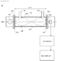
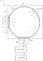
- Fig. 1 is a schematic diagram illustrating a schematic cross-sectional configuration of a gas detector.
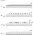
- Fig. 2 is a schematic diagram illustrating the schematic configuration of a window member incorporated into the gas detector, (a) illustrating a partial and schematic upper surface configuration of the window member, and (b) illustrating a schematic cross-sectional configuration of the window member.
- Fig. 3 is a process diagram illustrating a method for manufacturing the window member that is incorporated into the gas detector.
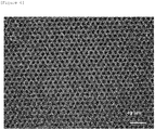
- Fig. 4 is a photograph showing the upper surface of the window member that is incorporated into the gas detector.
- Fig. 1 is a schematic diagram illustrating a schematic cross-sectional configuration of a gas detector.
- Fig. 2 is a schematic diagram illustrating the schematic configuration of a window member incorporated into the gas detector, (a) illustrating a partial and schematic upper surface configuration of the window member, and (b) illustrating a schematic cross-sectional configuration of the window member.
- Fig. 3 is a process diagram illustrating a
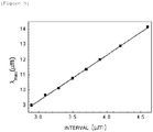
- FIG. 5 is a graph illustrating the relation between the interval between optical apertures of an conductive thin film of the window member incorporated into the gas detector and a wavelength ( ⁇ max ) of the maximum transmittance at a transmission peak in a transmission spectrum.
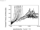
- Fig. 6 is a graph illustrating a comparison between transmission spectra of respective conductive thin films for the window member incorporated into the gas detector.
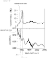
- Fig. 7A is a graph illustrating a transmission spectrum of the conductive thin film of the window member incorporated into the gas detector and an absorption spectrum of a target gas on the same wavelength axis, which shows that the transmission spectrum and the absorption spectrum are superimposed.
- FIG. 7B is a graph illustrating a transmission spectrum of the conductive thin film of the window member incorporated into the gas detector and an absorption spectrum of a target gas on the same wavelength axis, which shows that ⁇ trmax and ⁇ abmax match.
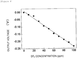
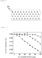
- Fig. 8 is a graph illustrating the relation between a target gas concentration and an output voltage.
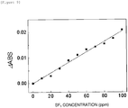
- Fig. 9 is a graph illustrating the relation between a target gas concentration and changes in absorbance.
- a gas detector 10 may include a gas cell 110 that is a container defining a cell internal space 130 for a target gas; a first window member 200; a second window member 300; a light source 410; a photodetector 420; a circuit 510; and a display 520.
- the gas detector 10 may use the photodetector 420 to detect light that has been emitted from the light source 410 and has propagated through the cell internal space 130.
- the gas detector 10 should not be limited to measure the concentration of a target gas, but may also be used to detect the presence of a target gas.
- the presence of a target gas may be detectable based on detecting a decrease in the light intensity of the propagated and received light.
- the gas detector may be configured to detect various kinds of gas.
- sulfur hexafluoride SF 6 is described as an example of the target gas in the present example, the target gas should not be limited thereto, and may be another greenhouse gas such as carbon dioxide, or may be a hazardous or non-hazardous gas other than a greenhouse gas.
- An absorption peak in the absorption spectrum of the currently focused sulfur hexafluoride SF 6 exhibits a maximum absorption at 10.5 ⁇ m.
- the light source 410 of the present example is configured to generate near-infrared light including a wavelength of 10.5 ⁇ m in accordance with the absorption peak of sulfur hexafluoride SF 6 .
- the photodetector 420 of the present example is configured to detect near-infrared light including the wavelength of 10.5 ⁇ m.
- the target gas is a gas having an absorption peak in a different wavelength band
- a wavelength/wavelength band of emitted light from the light source 410 and a wavelength/wavelength band that can be detected by the photodetector 420 will be adjusted in accordance therewith. That is, the disclosure of the present application should not be limited to gas detection in the near-infrared region.
- Light absorption can be expressed by molecular eigenvalue ⁇ concentration ⁇ optical path length. If the concentration is decreased to 1/10, a tenfold optical path length will be required.
- the greater length of the gas cell 110 may be adopted to achieve higher detection sensitivity for the target gas concentration, but will result in the increased size of the gas detector 10 in accordance with the greater length.
- the light source 410 may be configured to generate light having a wavelength belonging to an absorption peak in the absorption spectrum of the target gas. In the present example, as described above, the light source 410 generates near-infrared light.
- the specific configuration of the light source 410 is arbitrary, and for example the light source 410 may be a light source that generates pulsed light or a light source that may generate parallel light.
- a pulsed light source may be more preferable than a continuous light source because the light intensity is measured by the photodetector 420.
- a shutter might be used in combination with a continuous light source.
- An optical system such as a lens, a filter, a prism or a mirror may be incorporated into the light source 410, or an optical system such as a lens, a filter, a prism or a mirror may be optically coupled with the light source 410.
- the light source 410 may typically be a light emitting device such as an LED (light emitting diode) or an LD (laser diode), or a lamp. A wavelength of emitted light may also be adjusted by utilizing a fluorescent material.
- the light emitting device should not be limited to a silicon semiconductor device, and a compound semiconductor device may also be used as a light emitting device.
- the photodetector 420 may be configured to detect light of a wavelength belonging to the absorption peak in the absorption spectrum of the target gas.
- the specific configuration of the photodetector 420 may be arbitrary.
- An optical system such as a lens, a filter, a prism or a mirror may be incorporated into the photodetector 420, or an optical system such as a lens, a filter, a prism or a mirror may be optically coupled with the photodetector 420.
- the photodetector 420 may typically be a compound photodiode such as InGaAs that is sensitive to light in the infrared region, the photodetector 420 should not necessarily be limited thereto, and another light-sensitive element may be utilized. It is also possible to utilize an infrared absorption-type thermosensitive element.
- the light source 410 and the photodetector 420 may be arranged coaxially along an axis AX50, that is, an optical path between the light source 410 and the photodetector 420 may be a straight optical path. Accordingly, the built-in optical system in the gas detector 10 may be simplified, and simplification of assembling the product as well as lower product unit price may be achieved.
- the gas cell 110 may be a hollow container into which the target gas is supplied, and a hollow gas inlet 120 and a hollow gas outlet 140 may be provided thereto.
- the target gas may flow into the cell internal space 130 inside the gas cell 110 via the gas inlet 120, may flow through the cell internal space 130 from the light source 410 side to the photodetector 420 side, and may be discharged to outside via the gas outlet 140.
- the gas cell 110, the gas inlet 120 and the gas outlet 140 are, for example, cylindrically shaped, not necessarily limited thereto though.
- the window member 200 and the window member 300 may also be arranged coaxially along the axis AX50.
- the window member 200 may be a member that mediates/conveys the propagation of emitted light from the light source 410 to the cell internal space 130 side.
- the window member 200 is configured to be transparent to near-infrared light.
- the window member 200 is provided between the light source 410 and the cell internal space 130, and defines the cell internal space 130 from the light source 410 side.
- the window member 300 is a member that mediates/conveys the propagation of light that has emitted from the light source 410 and has propagated through the cell internal space 130, to the photodetector 420 side.
- the window member 300 is configured to be transparent to near-infrared light.
- the window member 300 is provided between the cell internal space 130 and the photodetector 420, and defines the cell internal space 130 from the photodetector 420 side.
- the front view shape of the window members 200 and 300 is arbitrary, and for example is a disc shape or a rectangular shape.
- the interval between the window member 200 and the window member 300 may indicate the cell length L110 of the gas cell 110 according to the present example.
- the cell length L110 is evidently shorter than the conventional products, and sufficient detection sensitivity for the target gas concentration can be secured even with a length of several centimeters thereof.
- the cell length L110 of the gas cell 110 can be shortened to around 10 microns. Accordingly, miniaturization of the gas detector 10 may be envisaged by utilizing a MEMS (micro electro mechanical systems) or the like.
- Fig. 2 is a schematic diagram illustrating the schematic configuration of the window member 200 incorporated into the gas detector 10, (a) illustrating a partial and schematic upper surface configuration of the window member 200, and (b) illustrating a schematic cross-sectional configuration of the window member 200. Note that the configuration of the window member 300 is substantially identical with that of the window member 200, and hence redundant descriptions shall be omitted herein.
- the window member 200 is an optical component in which an electrically conductive thin film 220 is provided on a support substrate 210, and a plurality of optical apertures 222 are regularly and two-dimensionally arranged in the conductive thin film 220.
- the support substrate 210 has a first main surface 211 at a side being exposed to the cell internal space 130, and a second main surface 212 at a side facing the light source 410.
- the first main surface 211 and the second main surface 212 are flat surfaces arranged in parallel one another, and the substrate thickness of the support substrate 210 is defined by these main surfaces.
- the first main surface 211 is also a light emission surface of the window member 200, while the second main surface 212 is also a light incidence surface of the window member 200.
- the conductive thin film 220 is formed on the first main surface 211 of the support substrate 210.
- the conductive thin film 220 is contactable with the target gas in the cell internal space 130, and the conductive thin film 220 is also provided on the optical path between the light source 410 and the photodetector 420.
- the support substrate 210 is a support substrate of the conductive thin film 220 and is transparent to the emitted light from the light source 410.
- the support substrate 210 is transparent to near-infrared light.
- An arbitrary material can be used as the material of the support substrate 210 as long as the material has transparency for the light belonging to an absorption peak in the absorption spectrum of the target gas.
- the support substrate 210 is a silicon substrate with a thickness of 450 to 550 ⁇ m. Since more near-infrared light will be absorbed if the thickness of the silicon substrate increases, it may be desirable to make the silicon substrate thin not to promote such absorption of near-infrared light.
- the thickness of the silicon substrate is 200 to 1000 ⁇ m.
- Another substrate made of germanium, sapphire or calcium fluoride or the like may also be useable.
- the conductive thin film 220 is a thin film made of an electrically conductive material that is exemplified by a metal, and the optical apertures 222 are regularly provided.
- the conductive thin film 220 is typically made of a material selected from the group consisting of silver, gold, copper, chromium, aluminum, iron, titanium, nickel, cobalt, rhodium, palladium, platinum, iridium, ruthenium, osmium, zinc, and rhenium.
- the thickness of the conductive thin film 220 is preferably 50 nm to 100 nm.
- Each optical aperture 222 is typically a space formed by partially removing the conductive thin film 220, but it may possibly filled with a transparent material.
- the arrangement interval of the optical apertures 222 can be changed depending on an absorption peak in the absorption spectrum of the target gas.
- the aperture diameter or maximum aperture width of the optical aperture 222 can be changed depending on the absorption peak in the absorption spectrum of the target gas.
- the shape of the optical apertures 222 should not be limited to the circular shape illustrated in the drawings.
- a transmission peak in the transmission spectrum of the conductive thin film 220 is adjusted by regularly providing the optical aperture 222.
- a transmission peak in the transmission spectrum of the conductive thin film can be explained by reference to an "anomalous transmission phenomenon".
- the “anomalous transmission phenomenon” is a phenomenon whereby an anomalous transmission peak appears in a transmission spectrum due to resonant coupling between incident light and surface plasmon polaritons (SPPs) on the surface of an electrically conductive member in which a periodic structure of regular apertures is provided.
- the studies by the inventor of the present application has revealed that by superimposing the transmission peak in the transmission spectrum of the conductive thin film 220 over the absorption peak in the absorption spectrum of the target gas along a wavelength axis, an adequate detection sensitivity for the target gas may be secured despite that the cell length L110 was shortened. This may be because the target gas and the emitted light of the light source 410 greatly interact at the surface of the conductive thin film 220 where the SPPs are excited, particularly at the edges of the optical apertures 222, in other words, the target gas absorbs a greater amount of the emitted light from the light source 410.
- the optical apertures 222 may be preferable to arrange the optical apertures 222 not in a four-sided lattice shape, but rather in a triangular lattice shape in which the interval between adjacent optical apertures 222 is set to be equal in plane.
- the optical apertures 222 are adjacent in a four-sided lattice shape, two transmission peaks will appear in the transmission spectrum of the conductive thin film 220 because the length of a diagonal line is longer than the length of each side in the square shape. This drawback may be eliminated by making the interval between adjacent optical apertures 222 equal in plane.
- Fig. 2(a) when Fig. 2 is viewed in front, there is an array L1 of optical apertures 222 arranged at a constant interval W7 in the transverse direction (first direction) (optical aperture array) and an array L2 of optical apertures 222 arranged at the constant interval W7 in the same transverse direction (optical aperture array).
- the array L1 and array L2 are adjacent in the vertical direction (second direction) when Fig. 2 is viewed in front. It will be understood that the optical apertures 222 of the array L2 are shifted in the rightward direction by an amount corresponding to W7/2 relative to the optical apertures 222 of the array L1 when Fig. 2 is viewed in front.
- the respective optical apertures 222 may be arranged at the respective vertices of respective triangular lattices, that is, equilateral triangles, and the intervals between adjacent optical apertures 222 are made uniform at the interval W7.
- the optical apertures 222 may be arranged in a zig-zag shape between the array L1 and the array L2. This also applies for the other arrays such as an array L3 and an array L4.
- the interval between the diagonally arranged adjacent optical apertures 222 in the arrays L3 and L4 has the interval W7 either.
- the aforementioned first and second directions are orthogonal one another, and a plane where the conductive thin film 220 exists is defined by these directions.
- the window member 200 may be manufactured based on a photolithography technique as shown in Fig. 3 .
- a sacrificial layer 230 made of, for example, a resist may be formed on the support substrate 210 (see (a) in Fig. 3 ); patterning of the sacrificial layer 230 may be then performed by selective light exposure and washing (see (b) in Fig. 3 ); a conductive layer 220' to be the conductive thin film 220 may be then formed on the patterned sacrificial layer 230 (see (c) in Fig.
- the sacrificial layer 230 on which the conductive layer 220' is deposited may be removed from the top of the support substrate 210 (see (d) in Fig. 3 ) to thereby obtain the window member 200 shown in Fig. 2 .
- laser processing or the like may be utilized instead of photolithography technology.
- Fig. 4 shows an enlarged photograph of the conductive thin film 220 of the window member 200.
- Fig. 5 is a graph illustrating the relation between the interval between the optical apertures 222 of the conductive thin film 220 of the window member 200 incorporated into the gas detector 10 and a wavelength ( ⁇ max ) of the maximum transmittance at a transmission peak in the transmission spectrum.
- Fig. 6 is a graph illustrating a comparison between transmission spectra of respective conductive thin films for the window member 200 incorporated into the gas detector 10.
- Fig. 5 shows results in a case where eight window member samples were used, and in which eight plots are approximated by a straight line.
- Fig. 6 illustrates the respective transmission spectra of the eight samples that relate to Fig. 5 .
- the wavelength ⁇ max shifts to the longer wavelength side as the interval between the optical apertures 222 increases, that is, the transmission peak in the transmission spectrum of the conductive thin film 220 shifts to the longer wavelength side.
- the interval between the optical apertures 222 explained herein indicates, for example, the interval W7 shown in Fig. 2 . It is understandable that an interval adjustment at the ⁇ m level causes a shift of the maximum intensity wavelength at the ⁇ m level.
- the window member of each sample has a single transmission peak for a transmittance in a band from visible red to near infrared (650 nm to 1150 nm).
- Figs. 7A and 7B are graphs in which a transmission spectrum of a conductive thin film at the window member incorporated into the gas detector and an absorption spectrum of the target gas are shown along the same wavelength axis.
- the transmission peak in the transmission spectrum of the conductive thin film 220 is superimposed over an absorption peak in the absorption spectrum of the target gas along the wavelength axis.
- the wavelength band of the transmission peak in the transmission spectrum of the conductive thin film 220 and the wavelength band of the absorption peak in the absorption spectrum of the target gas overlap, that is, include a common wavelength band.
- a wavelength ⁇ abmax at which the maximum absorption of the absorption peak in the absorption spectrum of the target gas occurs is 10.5 ⁇ m
- a wavelength ⁇ trmax at which the maximum transmittance at the transmission peak in the transmission spectrum of the conductive thin film 220 occurs is 10.46 ⁇ m.
- ⁇ abmax ⁇ 0.8 ⁇ ⁇ trmax ⁇ ⁇ abmax ⁇ 1.2 may be satisfied, preferably ⁇ abmax ⁇ 0.9 ⁇ ⁇ trmax ⁇ ⁇ abmax ⁇ 1.1 may be satisfied, and more preferably ⁇ abmax ⁇ 0.95 ⁇ ⁇ trmax ⁇ ⁇ abmax ⁇ 1.05 may be satisfied. In cases where such conditions were satisfied, adequate overlapping between the transmission peak in the transmission spectrum and the absorption peak in the absorption spectrum may be secured.
- the wavelength ⁇ abmax at which the maximum absorption of the absorption peak in the absorption spectrum of the target gas occurs is 10.5 ⁇ m
- the wavelength ⁇ trmax at which the maximum transmittance at the transmission peak in the transmission spectrum of the conductive thin film 220 occurs is 10.5 ⁇ m. It may be desirable that ⁇ abmax and ⁇ trmax completely match in this manner.
- the wavelength bandwidth of the absorption peak is sufficiently narrower than the wavelength bandwidth of the transmission peak, and the absorption peak is completely enclosed inside the wavelength bandwidth of the transmission peak.
- a mixed gas that includes two or more kinds of gases is adopted as the target gas, it is also conceivable that the wavelength bandwidth of the absorption peak will be wider than the wavelength bandwidth of the transmission peak.
- Fig. 8 illustrates that, in a case where SF 6 is used as the target gas under the present configuration, the voltage output changes linearly in accordance with an increase in the concentration of the target gas.
- Fig. 9 illustrates that, likewise, in a case where SF 6 is used as the target gas under the present configuration, a change in the absorbance ( ⁇ ABS) changes linearly in accordance with an increase in the concentration of the target gas. It is understandable that fluctuations in the ppm level of the target gas concentration of the target gas can also be accurately detected.
- the photodetector 420 shown in Fig. 1 typically includes a light detecting element such as a photodiode, an analog peripheral circuit that is electrically coupled to the light detecting element, and as an option, an A/D conversion circuit that converts an analog signal to a digital signal or the like.
- An output signal of the photodetector 420 shows the intensity of light detected by the photodetector 420.
- the circuit 510 includes an analog or digital circuit that processes output signals of the photodetector 420, and depending on the case, is comprised of a computer including a CPU or a memory. The circuit 510 determines and outputs a gas concentration value corresponding to the intensity of the aforementioned detected light based on an output signal of the photodetector 420.
- the output signal of the circuit 510 is transmitted to the display 520, and the display 520 displays the gas concentration value.
- the relation between the intensity of detected light and a gas concentration value may be experimentally determined in advance, and the correlation may be determined by utilizing a predetermined arithmetic expression or a look-up table.
- the target gas is supplied into the cell internal space 130 of the gas cell 110 through the gas inlet 120, and is discharged through the gas outlet 140.
- the light source 410 emits near-infrared pulsed light
- the near-infrared pulsed light is transmitted through the support substrate 210 of the window member 200, is transmitted through the conductive thin film 220, passes through the cell internal space 130, is transmitted through an conductive thin film 320 of the window member 300, and is transmitted through a support substrate 310 of the window member 300 to be incident on the photodetector 420.
- a predetermined proportion of the near-infrared pulsed light is absorbed by the support substrate of the respective window members.
- a predetermined proportion of the near-infrared pulsed light is reflected by the conductive thin film of the respective window members.
- a proportion of the near-infrared pulsed light that is in accordance with the amount/concentration of the target gas that is present in the cell internal space 130 of the gas cell 110 is absorbed by the target gas.
- the photodetector 420 detects the intensity of near-infrared light based on the amount of photoelectric current generated in the photodiode.
- the photodetector 420 converts the photoelectric current to a voltage and outputs to the circuit 510 a detection voltage having a magnitude reflecting the amount of photoelectric current.
- the circuit 510 processes the detection voltage and, for example, determines a target gas concentration value based on the detection voltage and outputs the target gas concentration value.
- a detection voltage value and a target gas concentration value can be experimentally determined beforehand (see Fig. 8 ).
- the display 520 displays the target gas concentration value transmitted from the circuit 510.
- the conductive thin films 220 and 320 in which the periodic structures of the optical apertures 222 are provided are provided on the optical path so as to come in contact with the target gas, and adequate light absorption by the target gas can be promoted in the vicinity of the conductive thin film 220, adequate detection sensitivity for the target gas can be secured without highly depending on the cell length L110 of the gas cell 110. Accordingly, even when the cell length L110 of the gas cell 110 shown in Fig. 1 is greatly shortened than before, adequate detection sensitivity for the target gas may be secured.
- a gas cell based on the existing NDIR method required that a length of "20 cm" or more should be secured as the length of a target gas flow path for detecting a 100ppm target gas.
- the cell length L110 of the gas cell 110 required to secure the same degree of sensitivity is "2 cm," and thus 1/10 downsizing compared to the existing method may be achieved.
- a plurality of conductive thin films two in the present example, namely, the conductive thin films 220 and 320, are provided on the optical path from the light source 410 to the photodetector 420. Accordingly, an interaction region between conductive thin films and target gas may be adequately secured, and adequate detection sensitivity for the target gas concentration can be secured.
- the number of conductive thin films arranged on the optical path is arbitrary, and two or more, for example, four or eight conductive thin films may be provided to secure the detection sensitivity. Note that an adverse effect of a decrease in transmittance may be avoided by making the number of conductive thin film eight or less. It will be apparent from the foregoing descriptions and from Figs. 7A and 7B that the overall transmittance is decreased by increasing the number of conductive thin films. Naturally, only one conductive thin film may be used.
- a conductive thin film may be provided at another location on the optical path between the light source 410 and the photodetector 420.
- an optical component having the same composition as the window member 200 and window member 300 may be provided as an intermediate element between the window member 200 and window member 300. That is, the window member is merely one example of an optical component.
- Fig. 10 is a schematic diagram illustrating a schematic cross-sectional configuration of a gas detector.
- a conductive thin film that is identical with the conductive thin film described in the first embodiment is provided on an inner side of the gas cell 110 and is arranged on the optical path from the light source 410 to the photodetector 420. Accordingly, a more adequate interaction area can be secured between the conductive thin film and the target gas. Similar advantageous effects as those in the first embodiment may be obtained in the present embodiment case either.
- a conductive thin film 240 that is identical with the conductive thin film described in the first embodiment is provided on a reflective inner side of the gas cell 110. Emitted light from the light source 410 diverges in the course of propagating along the optical path, and is reflected by the conductive thin film 240 on the inner side of the gas cell 110 and is also transmitted there-through and reflected by the reflective inner side.
- the inner side of the gas cell 110 has adequate reflectivity, and transmission of incident light through the gas cell 110 itself is inhibited.
- a transmission peak in the transmission spectrum of the conductive thin film 240 is superimposed over an absorption peak in the absorption spectrum of the target gas. Accordingly, absorption of near-infrared light by the target gas is promoted in the vicinity of the conductive thin film 240, and adequate detection sensitivity for the target gas may be secured regardless that the cell length L110 of the gas cell 110 is shortened.
- Fig. 11 is a schematic diagram illustrating a schematic cross-sectional configuration of a gas detector.
- the gas cell 110 has a spherical reflective inner side like an integrating sphere, and a conductive thin film that is identical with the conductive thin film described in the first embodiment is provided on a reflective spherical surface of the gas cell 110.
- the conductive thin film is arranged on the optical path from the light source 410 to the photodetector 420. A more adequate interaction area may be secured between the conductive thin film and the target gas. Similar advantageous effects as those in the first embodiment may be obtained in the present embodiment case either.
- the gas cell 110 is constructed to have a hollow cell internal space 130, and the cell internal space 130 is defined by the spherical surface. Note that a target gas inlet and a target gas outlet that are not shown in the drawing are communicated to the cell internal space 130 inside the gas cell 110. As shown schematically by arrows in Fig. 11 , inside the gas cell 110 the emitted light from the light source 410 is reflected by the conductive thin film 240 and is also transmitted there-through and is reflected by the reflective inner side of the gas cell 110. The inner side of the gas cell 110 is equipped with adequate reflectivity, and transmission of incident light through the gas cell 110 itself is inhibited.
- the constituent material of the gas cell 110 is, for example, one or more silicon substrates. For example, a hollow spherical space may be formed by causing hemispheric cavities formed in two flat silicon substrates to face each other.
- Fig. 12 is a schematic diagram illustrating a partial and schematic upper surface configuration of a window member incorporated into a gas detector.
- the shape of the optical apertures provided in the conductive thin film is circular, the aperture shape may be polygonal. In a case of a polygonal shape, it is predicted that interaction between emitted light from the light source 410 and target gas will be adequately promoted at the edges of the optical apertures because of an optical edge effect whereby light is liable to localize at the edges. Similar advantageous effects as in the first embodiment may be obtained in the present embodiment case either. Further, in comparison to a case where circular optical apertures are provided in the conductive thin film, it is expected that interaction between target gas and light will occur more adequately in the vicinity of the conductive thin film.
- triangular optical apertures 222 as one example of polygonal optical apertures are provided in the conductive thin film 220.
- the fourth embodiment is the same as the first embodiment.
- the optical apertures 222 may also be a square shape, a pentagonal shape, a hexagonal shape or the like, and should not be limited to a triangular shape.
- Figs. 13 and 14 are graphs each illustrating a comparison between inventive examples and a comparative example.
- the symbol ⁇ indicates an evaluation result of an example having an identical configuration with Fig. 1 , and this example is referred to as "Example 1 ".
- the symbol ⁇ indicates an evaluation result of an example in which one of the two conductive thin films is provided at a side not to contact the target gas in the configuration of Fig. 1 , and this example is referred to as "Example 2".
- the symbol ⁇ indicates an evaluation result of a comparative example in which both of the conductive thin films are respectively provided at a side not to contact the target gas.
- Example 1 the target gas was detected from 5 ppm. In the case of Example 2, the target gas was detected from 50 ppm. In the case of the comparative example, the target gas was detected from 80 ppm. The significance of exposing the conductive thin films to the target gas was thus confirmed. Further, the significance of adequately securing an interaction area between the conductive thin film and the target gas was confirmed.
- the used target gas was sulfur hexafluoride as described in the first embodiment.
- the cell length was 2 cm.
- a gas mixing apparatus was communicated to the gas inlet 120.
- a nitrogen cylinder and a target gas cylinder in which nitrogen and sulfur hexafluoride were mixed were connected to the gas mixing apparatus.
- the voltage output of the photodetector 420 was supplied to an oscilloscope, and a change in the output voltage was monitored.
- the required electric power was supplied to the light source, the photodetector and the oscilloscope from an electric power source.
- the light source 410 and the photodetector 420 may be provided at the same side.
- a light shield 251 may preferably be provided for inhibiting incidence of emitted light from the light source 410 onto the photodetector 420 without passing though the cell internal space 130.
- an opening is formed in the window member 200 by dicing, and the light shading unit is inserted into the opening.
- a reflector 252 is provided facing the window member 200, and accordingly emitted light from the light source 410 that has propagated through the cell internal space 130 can travel towards the photodetector 420.
- An optical component having the same structure as the window member 200 may be arranged instead of the reflection member 252.
- the conductive thin film on the substrate functions as a reflective layer, and interaction between the target gas and light may be promoted. It is preferable to set a V-shaped optical path as indicated by arrows in Fig. 15 .
- the gas detector 10 can be noticeably miniaturized.
- Light receiving/emitting devices in which a light receiving device and a light emitting device are integrated have been widely used, and an apparatus may be configured utilizing such light receiving/emitting devices.
- An ultimate integration may be achieved by utilizing a semiconductor process whereby a light receiving device and a light emitting device of semiconductor layered products are provided onto a common substrate of the support substrate 210.
Description
- The present disclosure relates to a gas detector, a gas detection method and an optical component.
- Gas detectors are utilized in various fields, such as in the fields of medical treatments, environmental measurements and various kinds of testing. Gas detectors are utilized, for example, to detect exhaust gas of air conditioners, exhaust gas of automobiles, exhaust gas from factories, leaking gas in domestic households, toxic gases such as gases associated with sick house syndrome, and odorous gas of raw garbage and pets and the like.
- Examples of gas detection methods include semiconductor type detection, contact combustion type detection, thermal conductivity type detection, and NDIR (non-dispersive infrared) type detection. The semiconductor type detection detects changes in electrical resistance caused by gas that is exposed to a semiconductor, and although this type of detection offers the advantages of being compact and having a high degree of mass productivity, there is the drawback that the semiconductor type detection lacks stability. The contact combustion type detection combusts gas inside an apparatus, and is limited to combustible gases. The thermal conductivity type detection detects a temperature change that is in accordance with a difference in the thermal conductivity of a gas, and has the drawback of low sensitivity. The NDIR type detection has an advantage of being applicable to various kinds of gases, having high sensitivity and providing long-term operational stability. However, there is a drawback that the apparatus size may be larger as sufficient optical path length is required.
- Document Yoshiaki Nishijima ET AL: "Selective enhancement of infrared absorption with metal hole arrays", Opt. Mater. Express, y September 2012 (2012-09-07), pages 1367-1377, XP055329236 discloses a metal hole array (MHA) structure useable for an application of gas detection.
-
Patent Literature 1 discloses, in its abstract, that, in order to keep the intensity of output light from an infrared light source 8 constant, an infrared detector 9B detects infrared light passing through an optical filter 10 B and having a wavelength that is not absorbed by gas , and controls an applied voltage to the infrared light source 8. - Document
US2005/0173635 A1 discloses a gas detector that includes at least two analytical detectors. Further a means for summing the signals detected by said two analytical detectors may be provided. - Document
US2012/0190997 A1 discloses a main stream gas analyzing device which obliquely angled infrared radiation source and detector. - Patent Literature 1: Japanese Patent Laid-Open No.
2010-139299 - For a method for measuring a target gas concentration in accordance with attenuation of light, typically the NDIR method, there is an inherent drawback that securing a long optical path length is required to improve the detection sensitivity.
- A gas detector according to an aspect of the present invention may include a space into which a target gas is supplied, the target gas exhibiting an absorption peak in an absorption spectrum; a light source configured to generate light having at least a wavelength belonging to the absorption peak; and a photodetector configured to detect the light that has emitted from the light source and has propagated through the space, wherein the gas detector may further include a conductive thin film in which a plurality of optical apertures are regularly arranged such that a transmission peak in a transmission spectrum is superimposed over the absorption peak in the absorption spectrum along a wavelength axis, and wherein the conductive thin film is provided on an optical path extending from the light source to the photodetector, and is provided so as to be contactable with the target gas within the space.
- In some embodiments, the plurality of optical apertures are two-dimensionally arranged at a predetermined interval along first and second directions that are orthogonal one another in a plane where the conductive thin film exists.
- In some embodiments, the plurality of optical apertures include a first and second optical aperture arrays in which the optical apertures are arranged along the first direction, the second optical aperture array being arranged adjacent to the first optical aperture array in the second direction, and arrangement positions of the optical apertures in the second optical aperture array being shifted in the first direction by an amount corresponding to a value of half of the predetermined interval relative to arrangement positions of the optical apertures in the first optical aperture array.
- In some embodiments, an interval between the adjacent optical apertures in the optical aperture array in which the optical apertures are arranged along the first direction and an interval between the optical aperture in said optical aperture array and the optical aperture in another optical aperture array adjacent thereto in a diagonal direction are equal.
- In some embodiments, the plurality of optical apertures are respectively provided at positions each corresponding to a vertex in a triangular shape that is a unit of a triangular lattice.
- In some embodiments, the conductive thin film is provided on a support substrate that is transparent to the emitted light from the light source.
- In some embodiments, the support substrate on which the conductive thin film is provided is a window member that mediates propagation of the emitted light from the light source to the space, or that mediates propagation of the light that has propagated through the space to the photodetector.
- In some embodiments, the conductive thin film is selected from a group consisting of silver, gold, copper, chromium, aluminum, iron, titanium, nickel, cobalt, rhodium, palladium, platinum, iridium, ruthenium, osmium, zinc, and rhenium.
- In some embodiments, the space is defined by a gas cell having a gas inlet and a gas outlet.
- In some embodiments, the space is defined by a gas cell having a gas inlet and a gas outlet, and the conductive thin film is provided on a reflective inner side of the gas cell.
- In some embodiments, the space is defined by a reflective spherical surface, and the conductive thin film is provided on the spherical surface.
- An optical component according to another aspect of the present invention may include a support substrate that is transparent to light having a wavelength belonging to an absorption peak of a target gas that exhibits the absorption peak in an absorption spectrum; and a conductive thin film that is provided on the support substrate, a plurality of optical apertures are regularly arranged such that a transmission peak in a transmission spectrum is superimposed over the absorption peak in the absorption spectrum along a wavelength axis.
- In some embodiment, in a case where the plurality of optical apertures are two-dimensionally arranged at a predetermined interval along first and second directions that are orthogonal one another in a plane where the conductive thin film exists, the plurality of optical apertures include first and second optical aperture arrays in which the optical apertures are arranged along the first direction, the second optical aperture array being arranged adjacent to the first optical aperture array in the second direction, and arrangement positions of the optical apertures in the second optical aperture array being shifted in the first direction by an amount corresponding to a value of half of the predetermined interval relative to arrangement positions of the optical apertures in the first optical aperture array.
- A gas detection method according to still another aspect of the present invention may include: irradiating, to a conductive thin film provided in a space to which a target gas having an absorption peak in an absorption spectrum is supplied, light having at least a wavelength belonging to the absorption peak, wherein a plurality of optical apertures is regularly arranged in the conductive thin film such that a transmission peak in a transmission spectrum is superimposed over the absorption peak in the absorption spectrum along a wavelength axis; and detecting the light that has propagated through the space via the conductive thin film.
- According to one aspect of the present invention it may be possible to secure sufficient gas detection sensitivity without greatly depending on an optical path length inside an apparatus.
-
- [
Fig. 1] Fig. 1 is a schematic diagram illustrating a schematic cross-sectional configuration of a gas detector according to a first embodiment of the present invention. - [
Fig. 2] Fig. 2 is a schematic diagram illustrating the schematic configuration of a window member incorporated into the gas detector according to the first embodiment of the present invention, (a) illustrating a partial and schematic upper surface configuration of the window member, and (b) illustrating a schematic cross-sectional configuration of the window member. - [
Fig. 3] Fig. 3 is a process diagram illustrating a method for manufacturing the window member incorporated into the gas detector according to the first embodiment of the present invention. - [
Fig. 4] Fig. 4 is a photograph showing the upper surface of the window member incorporated into the gas detector according to the first embodiment of the present invention. - [
Fig. 5] Fig. 5 is a graph illustrating the relation between an interval between optical apertures of an conductive thin film of the window member incorporated into the gas detector according to the first embodiment of the present invention and a wavelength (λmax) of the maximum transmittance at a transmission peak in a transmission spectrum. - [
Fig. 6] Fig. 6 is a graph illustrating a comparison between transmission spectra of respective conductive thin films for the window member incorporated into the gas detector according to the first embodiment of the present invention. - [
Fig. 7A] Fig. 7A is a graph illustrating a transmission spectrum of the conductive thin film of the window member incorporated into the gas detector according to the first embodiment of the present invention and an absorption spectrum of a target gas along the same wavelength axis, showing that the transmission spectrum and the absorption spectrum are superimposed. - [
Fig. 7B] Fig. 7B is a graph illustrating a transmission spectrum of the conductive thin film of the window member incorporated into the gas detector according to the first embodiment of the present invention and an absorption spectrum of a target gas along the same wavelength axis, showing that λtrmax and λabmax match. - [
Fig. 8] Fig. 8 is a graph illustrating the relation between a target gas concentration and an output voltage according to the first embodiment of the present invention. - [
Fig. 9] Fig. 9 is a graph illustrating the relation between a target gas concentration and changes in absorbance according to the first embodiment of the present invention. - [
Fig. 10] Fig. 10 is a schematic diagram illustrating a schematic cross-sectional configuration of a gas detector according to a second embodiment of the present invention. - [
Fig. 11] Fig. 11 is a schematic diagram illustrating a schematic cross-sectional configuration of a gas detector according to a third embodiment of the present invention. - [
Fig. 12] Fig. 12 is a schematic diagram illustrating a partial and schematic upper surface configuration of window member that is incorporated into a gas detector according to a fourth embodiment of the present invention. - [
Fig. 13] Fig. 13 is a graph illustrating a comparison between examples of the present invention and a comparative example. - [
Fig. 14] Fig. 14 is a graph illustrating comparison between examples of the present invention and a comparative example. - [
Fig. 15] Fig. 15 is a schematic diagram illustrating a modification of an embodiment of the present invention. - Hereunder, embodiments of the present invention will be described with reference to the accompanying drawings. The respective embodiments are not individually independent and may be suitably combined by those skilled in the art without providing excessive descriptions herein, and a synergistic effect resulting from such a combination may also be recognizable. In principle, duplicate descriptions among the embodiments shall be omitted.
- A first embodiment will be described referring to
Figs. 1 to 9 .Fig. 1 is a schematic diagram illustrating a schematic cross-sectional configuration of a gas detector.Fig. 2 is a schematic diagram illustrating the schematic configuration of a window member incorporated into the gas detector, (a) illustrating a partial and schematic upper surface configuration of the window member, and (b) illustrating a schematic cross-sectional configuration of the window member.Fig. 3 is a process diagram illustrating a method for manufacturing the window member that is incorporated into the gas detector.Fig. 4 is a photograph showing the upper surface of the window member that is incorporated into the gas detector.Fig. 5 is a graph illustrating the relation between the interval between optical apertures of an conductive thin film of the window member incorporated into the gas detector and a wavelength (λmax) of the maximum transmittance at a transmission peak in a transmission spectrum.Fig. 6 is a graph illustrating a comparison between transmission spectra of respective conductive thin films for the window member incorporated into the gas detector.Fig. 7A is a graph illustrating a transmission spectrum of the conductive thin film of the window member incorporated into the gas detector and an absorption spectrum of a target gas on the same wavelength axis, which shows that the transmission spectrum and the absorption spectrum are superimposed.Fig. 7B is a graph illustrating a transmission spectrum of the conductive thin film of the window member incorporated into the gas detector and an absorption spectrum of a target gas on the same wavelength axis, which shows that λtrmax and λabmax match.Fig. 8 is a graph illustrating the relation between a target gas concentration and an output voltage.Fig. 9 is a graph illustrating the relation between a target gas concentration and changes in absorbance. - As shown in
Fig. 1A , agas detector 10 may include agas cell 110 that is a container defining a cellinternal space 130 for a target gas; afirst window member 200; asecond window member 300; alight source 410; aphotodetector 420; acircuit 510; and adisplay 520. To measure the concentration of a target gas being supplied into the cellinternal space 130, thegas detector 10 may use thephotodetector 420 to detect light that has been emitted from thelight source 410 and has propagated through the cellinternal space 130. Note that thegas detector 10 should not be limited to measure the concentration of a target gas, but may also be used to detect the presence of a target gas. The presence of a target gas may be detectable based on detecting a decrease in the light intensity of the propagated and received light. The gas detector may be configured to detect various kinds of gas. - Although sulfur hexafluoride SF6 is described as an example of the target gas in the present example, the target gas should not be limited thereto, and may be another greenhouse gas such as carbon dioxide, or may be a hazardous or non-hazardous gas other than a greenhouse gas. An absorption peak in the absorption spectrum of the currently focused sulfur hexafluoride SF6 exhibits a maximum absorption at 10.5 µm. The
light source 410 of the present example is configured to generate near-infrared light including a wavelength of 10.5 µm in accordance with the absorption peak of sulfur hexafluoride SF6. Thephotodetector 420 of the present example is configured to detect near-infrared light including the wavelength of 10.5 µm. Note that, if the target gas is a gas having an absorption peak in a different wavelength band, a wavelength/wavelength band of emitted light from thelight source 410 and a wavelength/wavelength band that can be detected by thephotodetector 420 will be adjusted in accordance therewith. That is, the disclosure of the present application should not be limited to gas detection in the near-infrared region. - The longer the cell length L110 of the
gas cell 110 illustrated inFig. 1 will be, the higher the detection sensitivity for the target gas concentration will be. Light absorption can be expressed by molecular eigenvalue × concentration × optical path length. If the concentration is decreased to 1/10, a tenfold optical path length will be required. The greater length of thegas cell 110 may be adopted to achieve higher detection sensitivity for the target gas concentration, but will result in the increased size of thegas detector 10 in accordance with the greater length. As will be apparent from the following descriptions, according to the present embodiment, it may be possible to fundamentally solve this drawback that is inherent to a method for measuring a target gas concentration according to attenuation of light, such as the "NDIR method". - The
light source 410 may be configured to generate light having a wavelength belonging to an absorption peak in the absorption spectrum of the target gas. In the present example, as described above, thelight source 410 generates near-infrared light. The specific configuration of thelight source 410 is arbitrary, and for example thelight source 410 may be a light source that generates pulsed light or a light source that may generate parallel light. A pulsed light source may be more preferable than a continuous light source because the light intensity is measured by thephotodetector 420. However, a shutter might be used in combination with a continuous light source. An optical system such as a lens, a filter, a prism or a mirror may be incorporated into thelight source 410, or an optical system such as a lens, a filter, a prism or a mirror may be optically coupled with thelight source 410. Thelight source 410 may typically be a light emitting device such as an LED (light emitting diode) or an LD (laser diode), or a lamp. A wavelength of emitted light may also be adjusted by utilizing a fluorescent material. The light emitting device should not be limited to a silicon semiconductor device, and a compound semiconductor device may also be used as a light emitting device. - The
photodetector 420 may be configured to detect light of a wavelength belonging to the absorption peak in the absorption spectrum of the target gas. The specific configuration of thephotodetector 420 may be arbitrary. An optical system such as a lens, a filter, a prism or a mirror may be incorporated into thephotodetector 420, or an optical system such as a lens, a filter, a prism or a mirror may be optically coupled with thephotodetector 420. Although thephotodetector 420 may typically be a compound photodiode such as InGaAs that is sensitive to light in the infrared region, thephotodetector 420 should not necessarily be limited thereto, and another light-sensitive element may be utilized. It is also possible to utilize an infrared absorption-type thermosensitive element. - The
light source 410 and thephotodetector 420 may be arranged coaxially along an axis AX50, that is, an optical path between thelight source 410 and thephotodetector 420 may be a straight optical path. Accordingly, the built-in optical system in thegas detector 10 may be simplified, and simplification of assembling the product as well as lower product unit price may be achieved. - The
gas cell 110 may be a hollow container into which the target gas is supplied, and ahollow gas inlet 120 and ahollow gas outlet 140 may be provided thereto. The target gas may flow into the cellinternal space 130 inside thegas cell 110 via thegas inlet 120, may flow through the cellinternal space 130 from thelight source 410 side to thephotodetector 420 side, and may be discharged to outside via thegas outlet 140. Thegas cell 110, thegas inlet 120 and thegas outlet 140 are, for example, cylindrically shaped, not necessarily limited thereto though. - The
window member 200 and thewindow member 300 may also be arranged coaxially along the axis AX50. Thewindow member 200 may be a member that mediates/conveys the propagation of emitted light from thelight source 410 to the cellinternal space 130 side. In the present example, thewindow member 200 is configured to be transparent to near-infrared light. Thewindow member 200 is provided between thelight source 410 and the cellinternal space 130, and defines the cellinternal space 130 from thelight source 410 side. Thewindow member 300 is a member that mediates/conveys the propagation of light that has emitted from thelight source 410 and has propagated through the cellinternal space 130, to thephotodetector 420 side. In the present example thewindow member 300 is configured to be transparent to near-infrared light. Thewindow member 300 is provided between the cellinternal space 130 and thephotodetector 420, and defines the cellinternal space 130 from thephotodetector 420 side. The front view shape of thewindow members - The interval between the
window member 200 and thewindow member 300 may indicate the cell length L110 of thegas cell 110 according to the present example. In the present example, although depicted as being long inFig. 1 , the cell length L110 is evidently shorter than the conventional products, and sufficient detection sensitivity for the target gas concentration can be secured even with a length of several centimeters thereof. According to a simulation performed by the present inventor, the cell length L110 of thegas cell 110 can be shortened to around 10 microns. Accordingly, miniaturization of thegas detector 10 may be envisaged by utilizing a MEMS (micro electro mechanical systems) or the like. -
Fig. 2 is a schematic diagram illustrating the schematic configuration of thewindow member 200 incorporated into thegas detector 10, (a) illustrating a partial and schematic upper surface configuration of thewindow member 200, and (b) illustrating a schematic cross-sectional configuration of thewindow member 200. Note that the configuration of thewindow member 300 is substantially identical with that of thewindow member 200, and hence redundant descriptions shall be omitted herein. - As shown in
Fig. 2 , thewindow member 200 is an optical component in which an electrically conductivethin film 220 is provided on asupport substrate 210, and a plurality ofoptical apertures 222 are regularly and two-dimensionally arranged in the conductivethin film 220. Thesupport substrate 210 has a firstmain surface 211 at a side being exposed to the cellinternal space 130, and a secondmain surface 212 at a side facing thelight source 410. The firstmain surface 211 and the secondmain surface 212 are flat surfaces arranged in parallel one another, and the substrate thickness of thesupport substrate 210 is defined by these main surfaces. The firstmain surface 211 is also a light emission surface of thewindow member 200, while the secondmain surface 212 is also a light incidence surface of thewindow member 200. - The conductive
thin film 220 is formed on the firstmain surface 211 of thesupport substrate 210. The conductivethin film 220 is contactable with the target gas in the cellinternal space 130, and the conductivethin film 220 is also provided on the optical path between thelight source 410 and thephotodetector 420. - The
support substrate 210 is a support substrate of the conductivethin film 220 and is transparent to the emitted light from thelight source 410. In the present example, thesupport substrate 210 is transparent to near-infrared light. An arbitrary material can be used as the material of thesupport substrate 210 as long as the material has transparency for the light belonging to an absorption peak in the absorption spectrum of the target gas. In the present example, thesupport substrate 210 is a silicon substrate with a thickness of 450 to 550 µm. Since more near-infrared light will be absorbed if the thickness of the silicon substrate increases, it may be desirable to make the silicon substrate thin not to promote such absorption of near-infrared light. Preferably, the thickness of the silicon substrate is 200 to 1000 µm. Another substrate made of germanium, sapphire or calcium fluoride or the like may also be useable. - The conductive
thin film 220 is a thin film made of an electrically conductive material that is exemplified by a metal, and theoptical apertures 222 are regularly provided. The conductivethin film 220 is typically made of a material selected from the group consisting of silver, gold, copper, chromium, aluminum, iron, titanium, nickel, cobalt, rhodium, palladium, platinum, iridium, ruthenium, osmium, zinc, and rhenium. The thickness of the conductivethin film 220 is preferably 50 nm to 100 nm. Eachoptical aperture 222 is typically a space formed by partially removing the conductivethin film 220, but it may possibly filled with a transparent material. The arrangement interval of theoptical apertures 222 can be changed depending on an absorption peak in the absorption spectrum of the target gas. The aperture diameter or maximum aperture width of theoptical aperture 222 can be changed depending on the absorption peak in the absorption spectrum of the target gas. The shape of theoptical apertures 222 should not be limited to the circular shape illustrated in the drawings. - A transmission peak in the transmission spectrum of the conductive
thin film 220 is adjusted by regularly providing theoptical aperture 222. A transmission peak in the transmission spectrum of the conductive thin film can be explained by reference to an "anomalous transmission phenomenon". The "anomalous transmission phenomenon" is a phenomenon whereby an anomalous transmission peak appears in a transmission spectrum due to resonant coupling between incident light and surface plasmon polaritons (SPPs) on the surface of an electrically conductive member in which a periodic structure of regular apertures is provided. As will be apparent from the following descriptions, the studies by the inventor of the present application has revealed that by superimposing the transmission peak in the transmission spectrum of the conductivethin film 220 over the absorption peak in the absorption spectrum of the target gas along a wavelength axis, an adequate detection sensitivity for the target gas may be secured despite that the cell length L110 was shortened. This may be because the target gas and the emitted light of thelight source 410 greatly interact at the surface of the conductivethin film 220 where the SPPs are excited, particularly at the edges of theoptical apertures 222, in other words, the target gas absorbs a greater amount of the emitted light from thelight source 410. - Because the interval between the
optical apertures 222 influences the transmission peak in the transmission spectrum of the conductivethin film 220, it may be preferable to arrange theoptical apertures 222 not in a four-sided lattice shape, but rather in a triangular lattice shape in which the interval between adjacentoptical apertures 222 is set to be equal in plane. For example, in a case where theoptical apertures 222 are adjacent in a four-sided lattice shape, two transmission peaks will appear in the transmission spectrum of the conductivethin film 220 because the length of a diagonal line is longer than the length of each side in the square shape. This drawback may be eliminated by making the interval between adjacentoptical apertures 222 equal in plane. - Referring to
Fig. 2(a) , whenFig. 2 is viewed in front, there is an array L1 ofoptical apertures 222 arranged at a constant interval W7 in the transverse direction (first direction) (optical aperture array) and an array L2 ofoptical apertures 222 arranged at the constant interval W7 in the same transverse direction (optical aperture array). The array L1 and array L2 are adjacent in the vertical direction (second direction) whenFig. 2 is viewed in front. It will be understood that theoptical apertures 222 of the array L2 are shifted in the rightward direction by an amount corresponding to W7/2 relative to theoptical apertures 222 of the array L1 whenFig. 2 is viewed in front. - The respective
optical apertures 222 may be arranged at the respective vertices of respective triangular lattices, that is, equilateral triangles, and the intervals between adjacentoptical apertures 222 are made uniform at the interval W7. In other words, theoptical apertures 222 may be arranged in a zig-zag shape between the array L1 and the array L2. This also applies for the other arrays such as an array L3 and an array L4. For example, the interval between the diagonally arranged adjacentoptical apertures 222 in the arrays L3 and L4 has the interval W7 either. Note that, the aforementioned first and second directions are orthogonal one another, and a plane where the conductivethin film 220 exists is defined by these directions. - Any method for manufacturing the
window member 200 may be adoptable. For example, thewindow member 200 may be manufactured based on a photolithography technique as shown inFig. 3 . As shown inFig. 3 , asacrificial layer 230 made of, for example, a resist may be formed on the support substrate 210 (see (a) inFig. 3 ); patterning of thesacrificial layer 230 may be then performed by selective light exposure and washing (see (b) inFig. 3 ); a conductive layer 220' to be the conductivethin film 220 may be then formed on the patterned sacrificial layer 230 (see (c) inFig. 3 ); and thereafter thesacrificial layer 230 on which the conductive layer 220' is deposited may be removed from the top of the support substrate 210 (see (d) inFig. 3 ) to thereby obtain thewindow member 200 shown inFig. 2 . Note that laser processing or the like may be utilized instead of photolithography technology. -
Fig. 4 shows an enlarged photograph of the conductivethin film 220 of thewindow member 200. -
Fig. 5 is a graph illustrating the relation between the interval between theoptical apertures 222 of the conductivethin film 220 of thewindow member 200 incorporated into thegas detector 10 and a wavelength (λmax) of the maximum transmittance at a transmission peak in the transmission spectrum.Fig. 6 is a graph illustrating a comparison between transmission spectra of respective conductive thin films for thewindow member 200 incorporated into thegas detector 10.Fig. 5 shows results in a case where eight window member samples were used, and in which eight plots are approximated by a straight line.Fig. 6 illustrates the respective transmission spectra of the eight samples that relate toFig. 5 . - As shown in
Fig. 5 , the wavelength λmax shifts to the longer wavelength side as the interval between theoptical apertures 222 increases, that is, the transmission peak in the transmission spectrum of the conductivethin film 220 shifts to the longer wavelength side. The interval between theoptical apertures 222 explained herein indicates, for example, the interval W7 shown inFig. 2 . It is understandable that an interval adjustment at the µm level causes a shift of the maximum intensity wavelength at the µm level. - As shown in
Fig. 6 , it is recognizable that the window member of each sample has a single transmission peak for a transmittance in a band from visible red to near infrared (650 nm to 1150 nm). -
Figs. 7A and7B are graphs in which a transmission spectrum of a conductive thin film at the window member incorporated into the gas detector and an absorption spectrum of the target gas are shown along the same wavelength axis. In the present embodiment, as shown inFigs. 7A and7B , the transmission peak in the transmission spectrum of the conductivethin film 220 is superimposed over an absorption peak in the absorption spectrum of the target gas along the wavelength axis. In other words, the wavelength band of the transmission peak in the transmission spectrum of the conductivethin film 220 and the wavelength band of the absorption peak in the absorption spectrum of the target gas overlap, that is, include a common wavelength band. The studies and simulation results made and obtained by the inventor of the present application has revealed that, such a feature may promote the absorption of near-infrared light by the target gas in the vicinity of the conductive thin film, more specifically, and without any intention to limit the present invention, in the vicinity of side faces defining the optical apertures of the conductive thin film and in the vicinity of the surface of the first main surface of the conductive thin film at the side being exposed to the target gas so that an adequate detection sensitivity may be secured despite that the cell length L110 is shortened. - In the case illustrated in
Fig. 7A , a wavelength λabmax at which the maximum absorption of the absorption peak in the absorption spectrum of the target gas occurs is 10.5 µm, and a wavelength λtrmax at which the maximum transmittance at the transmission peak in the transmission spectrum of the conductivethin film 220 occurs is 10.46 µm. Thus, even when there is a difference between the wavelength λabmax and the wavelength λtrmax, it may be sufficient as long as overlapping of the transmission peak and the absorption peak is secured. - For example, when the wavelength at which the maximum absorption of the absorption peak in the absorption spectrum of the target gas occurs is taken as λabmax and the wavelength at which the maximum transmittance at the transmission peak in the transmission spectrum of the conductive thin film is taken as λtrmax, λabmax × 0.8 ≤ λtrmax ≤ λabmax × 1.2 may be satisfied, preferably λabmax × 0.9 ≤ λtrmax ≤ λabmax × 1.1 may be satisfied, and more preferably λabmax × 0.95 ≤ λtrmax ≤ λabmax × 1.05 may be satisfied. In cases where such conditions were satisfied, adequate overlapping between the transmission peak in the transmission spectrum and the absorption peak in the absorption spectrum may be secured.
- In the case illustrated in
Fig. 7B , the wavelength λabmax at which the maximum absorption of the absorption peak in the absorption spectrum of the target gas occurs is 10.5 µm, and the wavelength λtrmax at which the maximum transmittance at the transmission peak in the transmission spectrum of the conductivethin film 220 occurs is 10.5 ≤m. It may be desirable that λabmax and λtrmax completely match in this manner. In the case illustrated inFig. 7B , the wavelength bandwidth of the absorption peak is sufficiently narrower than the wavelength bandwidth of the transmission peak, and the absorption peak is completely enclosed inside the wavelength bandwidth of the transmission peak. When a mixed gas that includes two or more kinds of gases is adopted as the target gas, it is also conceivable that the wavelength bandwidth of the absorption peak will be wider than the wavelength bandwidth of the transmission peak. -
Fig. 8 illustrates that, in a case where SF6 is used as the target gas under the present configuration, the voltage output changes linearly in accordance with an increase in the concentration of the target gas.Fig. 9 illustrates that, likewise, in a case where SF6 is used as the target gas under the present configuration, a change in the absorbance (ΔABS) changes linearly in accordance with an increase in the concentration of the target gas. It is understandable that fluctuations in the ppm level of the target gas concentration of the target gas can also be accurately detected. - The
photodetector 420 shown inFig. 1 typically includes a light detecting element such as a photodiode, an analog peripheral circuit that is electrically coupled to the light detecting element, and as an option, an A/D conversion circuit that converts an analog signal to a digital signal or the like. An output signal of thephotodetector 420 shows the intensity of light detected by thephotodetector 420. Thecircuit 510 includes an analog or digital circuit that processes output signals of thephotodetector 420, and depending on the case, is comprised of a computer including a CPU or a memory. Thecircuit 510 determines and outputs a gas concentration value corresponding to the intensity of the aforementioned detected light based on an output signal of thephotodetector 420. The output signal of thecircuit 510 is transmitted to thedisplay 520, and thedisplay 520 displays the gas concentration value. The relation between the intensity of detected light and a gas concentration value may be experimentally determined in advance, and the correlation may be determined by utilizing a predetermined arithmetic expression or a look-up table. - Operation of the
gas detector 10 will now be described. The target gas is supplied into the cellinternal space 130 of thegas cell 110 through thegas inlet 120, and is discharged through thegas outlet 140. When thelight source 410 emits near-infrared pulsed light, the near-infrared pulsed light is transmitted through thesupport substrate 210 of thewindow member 200, is transmitted through the conductivethin film 220, passes through the cellinternal space 130, is transmitted through an conductivethin film 320 of thewindow member 300, and is transmitted through asupport substrate 310 of thewindow member 300 to be incident on thephotodetector 420. A predetermined proportion of the near-infrared pulsed light is absorbed by the support substrate of the respective window members. A predetermined proportion of the near-infrared pulsed light is reflected by the conductive thin film of the respective window members. A proportion of the near-infrared pulsed light that is in accordance with the amount/concentration of the target gas that is present in the cellinternal space 130 of thegas cell 110 is absorbed by the target gas. - The
photodetector 420 detects the intensity of near-infrared light based on the amount of photoelectric current generated in the photodiode. Thephotodetector 420 converts the photoelectric current to a voltage and outputs to the circuit 510 a detection voltage having a magnitude reflecting the amount of photoelectric current. Thecircuit 510 processes the detection voltage and, for example, determines a target gas concentration value based on the detection voltage and outputs the target gas concentration value. Those skilled in the art will understand that the relation between a detection voltage value and a target gas concentration value can be experimentally determined beforehand (seeFig. 8 ). Thedisplay 520 displays the target gas concentration value transmitted from thecircuit 510. - In the present embodiment, since the conductive
thin films optical apertures 222 are provided are provided on the optical path so as to come in contact with the target gas, and adequate light absorption by the target gas can be promoted in the vicinity of the conductivethin film 220, adequate detection sensitivity for the target gas can be secured without highly depending on the cell length L110 of thegas cell 110. Accordingly, even when the cell length L110 of thegas cell 110 shown inFig. 1 is greatly shortened than before, adequate detection sensitivity for the target gas may be secured. For example, a gas cell based on the existing NDIR method required that a length of "20 cm" or more should be secured as the length of a target gas flow path for detecting a 100ppm target gas. In the present embodiment, the cell length L110 of thegas cell 110 required to secure the same degree of sensitivity is "2 cm," and thus 1/10 downsizing compared to the existing method may be achieved. - In addition, according to the present embodiment, a plurality of conductive thin films, two in the present example, namely, the conductive
thin films light source 410 to thephotodetector 420. Accordingly, an interaction region between conductive thin films and target gas may be adequately secured, and adequate detection sensitivity for the target gas concentration can be secured. The number of conductive thin films arranged on the optical path is arbitrary, and two or more, for example, four or eight conductive thin films may be provided to secure the detection sensitivity. Note that an adverse effect of a decrease in transmittance may be avoided by making the number of conductive thin film eight or less. It will be apparent from the foregoing descriptions and fromFigs. 7A and7B that the overall transmittance is decreased by increasing the number of conductive thin films. Naturally, only one conductive thin film may be used. - It is not essential to provide a conductive thin film at the window member, and a conductive thin film may be provided at another location on the optical path between the
light source 410 and thephotodetector 420. For example, an optical component having the same composition as thewindow member 200 andwindow member 300 may be provided as an intermediate element between thewindow member 200 andwindow member 300. That is, the window member is merely one example of an optical component. - A second embodiment will now be described referring to
Fig. 10. Fig. 10 is a schematic diagram illustrating a schematic cross-sectional configuration of a gas detector. In the present embodiment, a conductive thin film that is identical with the conductive thin film described in the first embodiment is provided on an inner side of thegas cell 110 and is arranged on the optical path from thelight source 410 to thephotodetector 420. Accordingly, a more adequate interaction area can be secured between the conductive thin film and the target gas. Similar advantageous effects as those in the first embodiment may be obtained in the present embodiment case either. - As shown in
Fig. 10 , a conductivethin film 240 that is identical with the conductive thin film described in the first embodiment is provided on a reflective inner side of thegas cell 110. Emitted light from thelight source 410 diverges in the course of propagating along the optical path, and is reflected by the conductivethin film 240 on the inner side of thegas cell 110 and is also transmitted there-through and reflected by the reflective inner side. The inner side of thegas cell 110 has adequate reflectivity, and transmission of incident light through thegas cell 110 itself is inhibited. In the present embodiment also, a transmission peak in the transmission spectrum of the conductivethin film 240 is superimposed over an absorption peak in the absorption spectrum of the target gas. Accordingly, absorption of near-infrared light by the target gas is promoted in the vicinity of the conductivethin film 240, and adequate detection sensitivity for the target gas may be secured regardless that the cell length L110 of thegas cell 110 is shortened. - A third embodiment will now be described referring to
Fig. 11. Fig. 11 is a schematic diagram illustrating a schematic cross-sectional configuration of a gas detector. In the present embodiment, thegas cell 110 has a spherical reflective inner side like an integrating sphere, and a conductive thin film that is identical with the conductive thin film described in the first embodiment is provided on a reflective spherical surface of thegas cell 110. The conductive thin film is arranged on the optical path from thelight source 410 to thephotodetector 420. A more adequate interaction area may be secured between the conductive thin film and the target gas. Similar advantageous effects as those in the first embodiment may be obtained in the present embodiment case either. - As shown in
Fig. 11 , thegas cell 110 is constructed to have a hollow cellinternal space 130, and the cellinternal space 130 is defined by the spherical surface. Note that a target gas inlet and a target gas outlet that are not shown in the drawing are communicated to the cellinternal space 130 inside thegas cell 110. As shown schematically by arrows inFig. 11 , inside thegas cell 110 the emitted light from thelight source 410 is reflected by the conductivethin film 240 and is also transmitted there-through and is reflected by the reflective inner side of thegas cell 110. The inner side of thegas cell 110 is equipped with adequate reflectivity, and transmission of incident light through thegas cell 110 itself is inhibited. The constituent material of thegas cell 110 is, for example, one or more silicon substrates. For example, a hollow spherical space may be formed by causing hemispheric cavities formed in two flat silicon substrates to face each other. - A fourth embodiment will now be described referring to
Fig. 12. Fig. 12 is a schematic diagram illustrating a partial and schematic upper surface configuration of a window member incorporated into a gas detector. Although in the above described embodiments the shape of the optical apertures provided in the conductive thin film is circular, the aperture shape may be polygonal. In a case of a polygonal shape, it is predicted that interaction between emitted light from thelight source 410 and target gas will be adequately promoted at the edges of the optical apertures because of an optical edge effect whereby light is liable to localize at the edges. Similar advantageous effects as in the first embodiment may be obtained in the present embodiment case either. Further, in comparison to a case where circular optical apertures are provided in the conductive thin film, it is expected that interaction between target gas and light will occur more adequately in the vicinity of the conductive thin film. - As shown in
Fig. 12 , triangularoptical apertures 222 as one example of polygonal optical apertures are provided in the conductivethin film 220. In other respects, the fourth embodiment is the same as the first embodiment. Theoptical apertures 222 may also be a square shape, a pentagonal shape, a hexagonal shape or the like, and should not be limited to a triangular shape. -
Figs. 13 and14 are graphs each illustrating a comparison between inventive examples and a comparative example. The symbol ■ indicates an evaluation result of an example having an identical configuration withFig. 1 , and this example is referred to as "Example 1 ". The symbol ● indicates an evaluation result of an example in which one of the two conductive thin films is provided at a side not to contact the target gas in the configuration ofFig. 1 , and this example is referred to as "Example 2". The symbol ▲ indicates an evaluation result of a comparative example in which both of the conductive thin films are respectively provided at a side not to contact the target gas. - In the case of Example 1, the target gas was detected from 5 ppm. In the case of Example 2, the target gas was detected from 50 ppm. In the case of the comparative example, the target gas was detected from 80 ppm. The significance of exposing the conductive thin films to the target gas was thus confirmed. Further, the significance of adequately securing an interaction area between the conductive thin film and the target gas was confirmed.
- Note that the used target gas was sulfur hexafluoride as described in the first embodiment. The cell length was 2 cm. A gas mixing apparatus was communicated to the
gas inlet 120. A nitrogen cylinder and a target gas cylinder in which nitrogen and sulfur hexafluoride were mixed were connected to the gas mixing apparatus. The voltage output of thephotodetector 420 was supplied to an oscilloscope, and a change in the output voltage was monitored. The required electric power was supplied to the light source, the photodetector and the oscilloscope from an electric power source. - Based on the above teachings, various modifications may be added to the respective embodiments by those skilled in the art.
- As shown in
Fig. 15 , thelight source 410 and thephotodetector 420 may be provided at the same side. In this case, as shown inFig. 15 , alight shield 251 may preferably be provided for inhibiting incidence of emitted light from thelight source 410 onto thephotodetector 420 without passing though the cellinternal space 130. For example, an opening is formed in thewindow member 200 by dicing, and the light shading unit is inserted into the opening. Areflector 252 is provided facing thewindow member 200, and accordingly emitted light from thelight source 410 that has propagated through the cellinternal space 130 can travel towards thephotodetector 420. An optical component having the same structure as thewindow member 200 may be arranged instead of thereflection member 252. In such a case the conductive thin film on the substrate functions as a reflective layer, and interaction between the target gas and light may be promoted. It is preferable to set a V-shaped optical path as indicated by arrows inFig. 15 . In the case illustrated inFig. 15 , thegas detector 10 can be noticeably miniaturized. Light receiving/emitting devices in which a light receiving device and a light emitting device are integrated have been widely used, and an apparatus may be configured utilizing such light receiving/emitting devices. An ultimate integration may be achieved by utilizing a semiconductor process whereby a light receiving device and a light emitting device of semiconductor layered products are provided onto a common substrate of thesupport substrate 210. -
- 10 Gas detector
- 110 Gas cell
- 120 Gas inlet
- 130 Cell internal space
- 140 Gas outlet
- 200 Window member
- 210 Support substrate
- 220 Electrically conductive thin film
- 300 Window member
- 310 Support substrate
- 320 Electrically conductive thin film
- 410 Light source
- 420 Photodetector
- 510 Circuit
- 520 Display
Claims (8)
- A gas detector (10), comprising:a space (130) into which a target gas is supplied, the space (130) being defined by a gas cell (110) having a gas inlet (120) and a gas outlet (140), and the target gas exhibiting an absorption peak in an absorption spectrum;a light source (410) configured to generate light having at least a wavelength belonging to the absorption peak;a photodetector (420) configured to detect the light that has been emitted from the light source (410) and has propagated through the space (130);a support substrate (210) that is arranged on an optical path extending from the light source (410) to the photodetector (420);
characterized in thata conductive thin film (220, 240, 320) on which surface plasmon polaritons are excited in response to the light from the light source (410) and in which a plurality of optical apertures (222) are regularly arranged such that a transmission peak in a transmission spectrum is superimposed over the absorption peak in the absorption spectrum along a wavelength axis, the transmission peak being in accordance with an interval of the regularly arranged optical apertures (222), the conductive thin film (220, 240, 320) being able to transmit light corresponding to the transmission peak; ,wherein the conductive thin film (220, 320) is provided on the support substrate (210) to configure a window member (200, 300) of the gas cell (110) that mediates propagation of the emitted light from the light source (410) to the defined space (130), or that mediates propagation of the light that has propagated through the defined space (130) to the photodetector (420) the conductive thin film (220, 320) being provided so as to be contactable with the target gas within the defined space (130). - The gas detector of claim 1, wherein the plurality of optical apertures (222) are two-dimensionally arranged at a predetermined interval along first and second directions that are orthogonal one another in a plane where the conductive thin film (220, 240, 320) exists.
- The gas detector of claim 2, wherein the plurality of optical apertures (222) include a first and second optical aperture arrays (L1-L4) in which the optical apertures (222) are arranged along the first direction, the second optical aperture array being arranged adjacent to the first optical aperture array (L1,L3) in the second direction, and arrangement positions of the optical apertures (222) in the second optical aperture array (L2,L4) being shifted in the first direction by an amount corresponding to a value of half of the predetermined interval relative to arrangement positions of the optical apertures (222) in the first optical aperture array.
- The gas detector of claim 2 or 3, wherein an interval between the adjacent optical apertures (222) in the optical aperture array (L1-L4) in which the optical apertures (222) are arranged along the first direction and an interval between the optical aperture (222) in said optical aperture array (L1-L4) and the optical aperture (222) in another optical aperture array (L1-L4) adjacent thereto in a diagonal direction are equal.
- The gas detector according to any one of claims 1 to 4, wherein the plurality of optical apertures (222) are respectively provided at positions each corresponding to a vertex in a triangular shape that is a unit of a triangular lattice.
- The gas detector according to any one of claims 1 to 5, wherein the conductive thin film (220, 240, 320) is selected from a group consisting of silver, gold, copper, chromium, aluminum, iron, titanium, nickel, cobalt, rhodium, palladium, platinum, iridium, ruthenium, osmium, zinc, and rhenium.
- The gas detector according to any one of claims 1 to 7, wherein the conductive thin film (240) is provided on a reflective inner side of the gas cell (110).
- The gas detector according to any one of claims 1 to 6, wherein the space (130) is defined by a reflective spherical surface of the gas cell (110), and the conductive thin film (240) is provided on the spherical surface.
Applications Claiming Priority (2)
| Application Number | Priority Date | Filing Date | Title |
|---|---|---|---|
| JP2013087683A JP6063333B2 (en) | 2013-04-18 | 2013-04-18 | Gas detection device, gas detection method, and optical component |
| PCT/JP2014/060229 WO2014171372A1 (en) | 2013-04-18 | 2014-04-08 | Gas detection device, gas detection method, and optical component |
Publications (3)
| Publication Number | Publication Date |
|---|---|
| EP2988114A1 EP2988114A1 (en) | 2016-02-24 |
| EP2988114A4 EP2988114A4 (en) | 2017-01-25 |
| EP2988114B1 true EP2988114B1 (en) | 2018-02-28 |
Family
ID=51731315
Family Applications (1)
| Application Number | Title | Priority Date | Filing Date |
|---|---|---|---|
| EP14784955.8A Not-in-force EP2988114B1 (en) | 2013-04-18 | 2014-04-08 | Gas detection device |
Country Status (4)
| Country | Link |
|---|---|
| US (1) | US9791366B2 (en) |
| EP (1) | EP2988114B1 (en) |
| JP (1) | JP6063333B2 (en) |
| WO (1) | WO2014171372A1 (en) |
Families Citing this family (5)
| Publication number | Priority date | Publication date | Assignee | Title |
|---|---|---|---|---|
| US9759652B2 (en) * | 2015-02-28 | 2017-09-12 | Board Of Supervisors Of Louisiana State University And Agricultural And Mechanical College | Quantum dot light emitting diodes for multiplex gas sensing |
| CN106353277B (en) * | 2016-08-29 | 2020-07-14 | 吉林大学 | Gas absorption cell based on copper scandium oxygen infrared transparent conducting film |
| CN110462380B (en) * | 2017-03-31 | 2022-05-24 | 国立大学法人横浜国立大学 | Hydrogen detection element, method for manufacturing hydrogen detection element, and hydrogen detection device |
| US10656080B2 (en) | 2018-07-06 | 2020-05-19 | Asahi Kasei Microdevices Corporation | Gas detection apparatus |
| US20200378892A1 (en) * | 2019-05-28 | 2020-12-03 | Si-Ware Systems | Integrated device for fluid analysis |
Family Cites Families (12)
| Publication number | Priority date | Publication date | Assignee | Title |
|---|---|---|---|---|
| JPH06102184A (en) * | 1992-09-18 | 1994-04-15 | Senri Oyo Keisoku Kenkyusho:Kk | Chemical sensor |
| US20030023181A1 (en) * | 2001-07-26 | 2003-01-30 | Mault James R. | Gas analyzer of the fluorescent-film type particularly useful for respiratory analysis |
| US6998613B2 (en) * | 2003-04-22 | 2006-02-14 | Raytheon Company | Integrated spectroscopic microbolometer with microfilter arrays |
| US7132657B2 (en) | 2004-02-09 | 2006-11-07 | Sensor Electronics Corporation | Infrared gas detector |
| US20060044562A1 (en) * | 2004-08-25 | 2006-03-02 | Norsk Elektro Optikk As | Gas monitor |
| JP2007218900A (en) * | 2006-01-18 | 2007-08-30 | Canon Inc | Element for detecting target substance |
| WO2007083817A1 (en) | 2006-01-18 | 2007-07-26 | Canon Kabushiki Kaisha | Target substance-detecting element |
| JP2010139299A (en) | 2008-12-10 | 2010-06-24 | Akebono Brake Ind Co Ltd | Gas sensor |
| JP5452140B2 (en) * | 2009-09-03 | 2014-03-26 | 日本航空電子工業株式会社 | Surface plasmon resonance element for hydrogen detection, surface plasmon resonance optical hydrogen detector, and method for optically detecting hydrogen using surface plasmon resonance |
| JP5971789B2 (en) * | 2010-08-31 | 2016-08-17 | 国立研究開発法人物質・材料研究機構 | Fabrication method of fiber probe |
| US20120190997A1 (en) * | 2011-01-21 | 2012-07-26 | Carefusion 2200, Inc. | Main stream gas analyzing device |
| JP6102184B2 (en) | 2012-10-31 | 2017-03-29 | 日立化成株式会社 | Light control element, light control device, light control film drive method, light control film drive device |
-
2013
- 2013-04-18 JP JP2013087683A patent/JP6063333B2/en active Active
-
2014
- 2014-04-08 WO PCT/JP2014/060229 patent/WO2014171372A1/en active Application Filing
- 2014-04-08 US US14/784,548 patent/US9791366B2/en active Active
- 2014-04-08 EP EP14784955.8A patent/EP2988114B1/en not_active Not-in-force
Non-Patent Citations (1)
| Title |
|---|
| None * |
Also Published As
| Publication number | Publication date |
|---|---|
| US9791366B2 (en) | 2017-10-17 |
| US20160054220A1 (en) | 2016-02-25 |
| JP2014211362A (en) | 2014-11-13 |
| EP2988114A4 (en) | 2017-01-25 |
| JP6063333B2 (en) | 2017-01-18 |
| EP2988114A1 (en) | 2016-02-24 |
| WO2014171372A1 (en) | 2014-10-23 |
Similar Documents
| Publication | Publication Date | Title |
|---|---|---|
| EP2988114B1 (en) | Gas detection device | |
| CN101706434B (en) | Fluorophototmeter capable of detecting light absorption or light transmission | |
| US5923035A (en) | Infrared absorption measuring device | |
| CA2771670C (en) | Remote sensing of gas leaks | |
| CN101105449A (en) | Double light source double sensitive element infra-red multiple gas detection sensor | |
| CN201689050U (en) | Fluophotometer capable of detecting light absorption or light transmission | |
| US10036702B2 (en) | Method, device and sensor for determining an absorption behavior of a medium | |
| EP3480570A1 (en) | Pyranometer and photometric device | |
| CN111929267A (en) | Gas sensor with low power consumption | |
| JP2007201475A (en) | Narrow band transmission filter for euv radiation | |
| US20190186988A1 (en) | Pyranometer and photometric device | |
| JP6516484B2 (en) | Dissolved matter concentration measuring device | |
| CN209961651U (en) | Multi-angle particulate matter detects photometer | |
| US10114154B2 (en) | Optical head for receiving light and optical system using the same | |
| US9865763B2 (en) | Method, a semiconductor detector, and a detector arrangement, for the detection of sunlight | |
| US11892396B2 (en) | Gas sensor with two switchable filters and method for operating such a gas sensor | |
| WO2018101690A1 (en) | Optical gas-sensor using multiple inner reflection | |
| CN110261350A (en) | A kind of optical sensor system and sensing testing method | |
| RU2698961C1 (en) | Smoke detector | |
| US10684214B2 (en) | Optical cavity with strong dynamic | |
| CN214066923U (en) | Non-dispersive infrared long optical path measuring cell combined gas measuring system | |
| CA2934093A1 (en) | Remote sensing of natural gas leaks | |
| RU169833U1 (en) | Matched spectrum optical radiation source for measuring the concentration of methane molecules in the atmosphere | |
| KR20090004271A (en) | Optical gas sensors | |
| RU171814U1 (en) | Optical radiation source for measuring the concentration of methane molecules in the gas phase |
Legal Events
| Date | Code | Title | Description |
|---|---|---|---|
| PUAI | Public reference made under article 153(3) epc to a published international application that has entered the european phase |
Free format text: ORIGINAL CODE: 0009012 |
|
| 17P | Request for examination filed |
Effective date: 20151102 |
|
| AK | Designated contracting states |
Kind code of ref document: A1 Designated state(s): AL AT BE BG CH CY CZ DE DK EE ES FI FR GB GR HR HU IE IS IT LI LT LU LV MC MK MT NL NO PL PT RO RS SE SI SK SM TR |
|
| AX | Request for extension of the european patent |
Extension state: BA ME |
|
| DAX | Request for extension of the european patent (deleted) | ||
| REG | Reference to a national code |
Ref country code: DE Ref legal event code: R079 Ref document number: 602014021693 Country of ref document: DE Free format text: PREVIOUS MAIN CLASS: G01N0021610000 Ipc: G01N0021552000 |
|
| A4 | Supplementary search report drawn up and despatched |
Effective date: 20170103 |
|
| RIC1 | Information provided on ipc code assigned before grant |
Ipc: G01N 21/3504 20140101ALI20161221BHEP Ipc: G01N 21/359 20140101ALI20161221BHEP Ipc: G01N 21/552 20140101AFI20161221BHEP |
|
| GRAP | Despatch of communication of intention to grant a patent |
Free format text: ORIGINAL CODE: EPIDOSNIGR1 |
|
| INTG | Intention to grant announced |
Effective date: 20170914 |
|
| RIN1 | Information on inventor provided before grant (corrected) |
Inventor name: NISHIJIMA,YOSHIAKI Inventor name: ADACHI,YUTA |
|
| GRAS | Grant fee paid |
Free format text: ORIGINAL CODE: EPIDOSNIGR3 |
|
| GRAA | (expected) grant |
Free format text: ORIGINAL CODE: 0009210 |
|
| AK | Designated contracting states |
Kind code of ref document: B1 Designated state(s): AL AT BE BG CH CY CZ DE DK EE ES FI FR GB GR HR HU IE IS IT LI LT LU LV MC MK MT NL NO PL PT RO RS SE SI SK SM TR |
|
| REG | Reference to a national code |
Ref country code: GB Ref legal event code: FG4D Ref country code: CH Ref legal event code: EP |
|
| REG | Reference to a national code |
Ref country code: AT Ref legal event code: REF Ref document number: 974685 Country of ref document: AT Kind code of ref document: T Effective date: 20180315 |
|
| REG | Reference to a national code |
Ref country code: IE Ref legal event code: FG4D |
|
| REG | Reference to a national code |
Ref country code: DE Ref legal event code: R096 Ref document number: 602014021693 Country of ref document: DE |
|
| REG | Reference to a national code |
Ref country code: NL Ref legal event code: MP Effective date: 20180228 |
|
| REG | Reference to a national code |
Ref country code: LT Ref legal event code: MG4D |
|
| REG | Reference to a national code |
Ref country code: AT Ref legal event code: MK05 Ref document number: 974685 Country of ref document: AT Kind code of ref document: T Effective date: 20180228 |
|
| PG25 | Lapsed in a contracting state [announced via postgrant information from national office to epo] |
Ref country code: LT Free format text: LAPSE BECAUSE OF FAILURE TO SUBMIT A TRANSLATION OF THE DESCRIPTION OR TO PAY THE FEE WITHIN THE PRESCRIBED TIME-LIMIT Effective date: 20180228 Ref country code: CY Free format text: LAPSE BECAUSE OF FAILURE TO SUBMIT A TRANSLATION OF THE DESCRIPTION OR TO PAY THE FEE WITHIN THE PRESCRIBED TIME-LIMIT Effective date: 20180228 Ref country code: NO Free format text: LAPSE BECAUSE OF FAILURE TO SUBMIT A TRANSLATION OF THE DESCRIPTION OR TO PAY THE FEE WITHIN THE PRESCRIBED TIME-LIMIT Effective date: 20180528 Ref country code: FI Free format text: LAPSE BECAUSE OF FAILURE TO SUBMIT A TRANSLATION OF THE DESCRIPTION OR TO PAY THE FEE WITHIN THE PRESCRIBED TIME-LIMIT Effective date: 20180228 Ref country code: NL Free format text: LAPSE BECAUSE OF FAILURE TO SUBMIT A TRANSLATION OF THE DESCRIPTION OR TO PAY THE FEE WITHIN THE PRESCRIBED TIME-LIMIT Effective date: 20180228 Ref country code: HR Free format text: LAPSE BECAUSE OF FAILURE TO SUBMIT A TRANSLATION OF THE DESCRIPTION OR TO PAY THE FEE WITHIN THE PRESCRIBED TIME-LIMIT Effective date: 20180228 Ref country code: ES Free format text: LAPSE BECAUSE OF FAILURE TO SUBMIT A TRANSLATION OF THE DESCRIPTION OR TO PAY THE FEE WITHIN THE PRESCRIBED TIME-LIMIT Effective date: 20180228 |
|
| PG25 | Lapsed in a contracting state [announced via postgrant information from national office to epo] |
Ref country code: RS Free format text: LAPSE BECAUSE OF FAILURE TO SUBMIT A TRANSLATION OF THE DESCRIPTION OR TO PAY THE FEE WITHIN THE PRESCRIBED TIME-LIMIT Effective date: 20180228 Ref country code: LV Free format text: LAPSE BECAUSE OF FAILURE TO SUBMIT A TRANSLATION OF THE DESCRIPTION OR TO PAY THE FEE WITHIN THE PRESCRIBED TIME-LIMIT Effective date: 20180228 Ref country code: SE Free format text: LAPSE BECAUSE OF FAILURE TO SUBMIT A TRANSLATION OF THE DESCRIPTION OR TO PAY THE FEE WITHIN THE PRESCRIBED TIME-LIMIT Effective date: 20180228 Ref country code: GR Free format text: LAPSE BECAUSE OF FAILURE TO SUBMIT A TRANSLATION OF THE DESCRIPTION OR TO PAY THE FEE WITHIN THE PRESCRIBED TIME-LIMIT Effective date: 20180529 Ref country code: BG Free format text: LAPSE BECAUSE OF FAILURE TO SUBMIT A TRANSLATION OF THE DESCRIPTION OR TO PAY THE FEE WITHIN THE PRESCRIBED TIME-LIMIT Effective date: 20180528 Ref country code: AT Free format text: LAPSE BECAUSE OF FAILURE TO SUBMIT A TRANSLATION OF THE DESCRIPTION OR TO PAY THE FEE WITHIN THE PRESCRIBED TIME-LIMIT Effective date: 20180228 |
|
| PG25 | Lapsed in a contracting state [announced via postgrant information from national office to epo] |
Ref country code: AL Free format text: LAPSE BECAUSE OF FAILURE TO SUBMIT A TRANSLATION OF THE DESCRIPTION OR TO PAY THE FEE WITHIN THE PRESCRIBED TIME-LIMIT Effective date: 20180228 Ref country code: IT Free format text: LAPSE BECAUSE OF FAILURE TO SUBMIT A TRANSLATION OF THE DESCRIPTION OR TO PAY THE FEE WITHIN THE PRESCRIBED TIME-LIMIT Effective date: 20180228 Ref country code: EE Free format text: LAPSE BECAUSE OF FAILURE TO SUBMIT A TRANSLATION OF THE DESCRIPTION OR TO PAY THE FEE WITHIN THE PRESCRIBED TIME-LIMIT Effective date: 20180228 Ref country code: PL Free format text: LAPSE BECAUSE OF FAILURE TO SUBMIT A TRANSLATION OF THE DESCRIPTION OR TO PAY THE FEE WITHIN THE PRESCRIBED TIME-LIMIT Effective date: 20180228 Ref country code: RO Free format text: LAPSE BECAUSE OF FAILURE TO SUBMIT A TRANSLATION OF THE DESCRIPTION OR TO PAY THE FEE WITHIN THE PRESCRIBED TIME-LIMIT Effective date: 20180228 |
|
| REG | Reference to a national code |
Ref country code: DE Ref legal event code: R097 Ref document number: 602014021693 Country of ref document: DE |
|
| PG25 | Lapsed in a contracting state [announced via postgrant information from national office to epo] |
Ref country code: SK Free format text: LAPSE BECAUSE OF FAILURE TO SUBMIT A TRANSLATION OF THE DESCRIPTION OR TO PAY THE FEE WITHIN THE PRESCRIBED TIME-LIMIT Effective date: 20180228 Ref country code: CZ Free format text: LAPSE BECAUSE OF FAILURE TO SUBMIT A TRANSLATION OF THE DESCRIPTION OR TO PAY THE FEE WITHIN THE PRESCRIBED TIME-LIMIT Effective date: 20180228 Ref country code: MC Free format text: LAPSE BECAUSE OF FAILURE TO SUBMIT A TRANSLATION OF THE DESCRIPTION OR TO PAY THE FEE WITHIN THE PRESCRIBED TIME-LIMIT Effective date: 20180228 Ref country code: SM Free format text: LAPSE BECAUSE OF FAILURE TO SUBMIT A TRANSLATION OF THE DESCRIPTION OR TO PAY THE FEE WITHIN THE PRESCRIBED TIME-LIMIT Effective date: 20180228 Ref country code: DK Free format text: LAPSE BECAUSE OF FAILURE TO SUBMIT A TRANSLATION OF THE DESCRIPTION OR TO PAY THE FEE WITHIN THE PRESCRIBED TIME-LIMIT Effective date: 20180228 |
|
| REG | Reference to a national code |
Ref country code: CH Ref legal event code: PL |
|
| REG | Reference to a national code |
Ref country code: BE Ref legal event code: MM Effective date: 20180430 |
|
| PLBE | No opposition filed within time limit |
Free format text: ORIGINAL CODE: 0009261 |
|
| STAA | Information on the status of an ep patent application or granted ep patent |
Free format text: STATUS: NO OPPOSITION FILED WITHIN TIME LIMIT |
|
| REG | Reference to a national code |
Ref country code: IE Ref legal event code: MM4A |
|
| GBPC | Gb: european patent ceased through non-payment of renewal fee |
Effective date: 20180528 |
|
| PG25 | Lapsed in a contracting state [announced via postgrant information from national office to epo] |
Ref country code: LU Free format text: LAPSE BECAUSE OF NON-PAYMENT OF DUE FEES Effective date: 20180408 |
|
| 26N | No opposition filed |
Effective date: 20181129 |
|
| PG25 | Lapsed in a contracting state [announced via postgrant information from national office to epo] |
Ref country code: SI Free format text: LAPSE BECAUSE OF FAILURE TO SUBMIT A TRANSLATION OF THE DESCRIPTION OR TO PAY THE FEE WITHIN THE PRESCRIBED TIME-LIMIT Effective date: 20180228 Ref country code: CH Free format text: LAPSE BECAUSE OF NON-PAYMENT OF DUE FEES Effective date: 20180430 Ref country code: LI Free format text: LAPSE BECAUSE OF NON-PAYMENT OF DUE FEES Effective date: 20180430 Ref country code: BE Free format text: LAPSE BECAUSE OF NON-PAYMENT OF DUE FEES Effective date: 20180430 |
|
| PG25 | Lapsed in a contracting state [announced via postgrant information from national office to epo] |
Ref country code: FR Free format text: LAPSE BECAUSE OF NON-PAYMENT OF DUE FEES Effective date: 20180428 Ref country code: IE Free format text: LAPSE BECAUSE OF NON-PAYMENT OF DUE FEES Effective date: 20180408 Ref country code: GB Free format text: LAPSE BECAUSE OF NON-PAYMENT OF DUE FEES Effective date: 20180528 |
|
| PG25 | Lapsed in a contracting state [announced via postgrant information from national office to epo] |
Ref country code: MT Free format text: LAPSE BECAUSE OF NON-PAYMENT OF DUE FEES Effective date: 20180408 |
|
| PG25 | Lapsed in a contracting state [announced via postgrant information from national office to epo] |
Ref country code: TR Free format text: LAPSE BECAUSE OF FAILURE TO SUBMIT A TRANSLATION OF THE DESCRIPTION OR TO PAY THE FEE WITHIN THE PRESCRIBED TIME-LIMIT Effective date: 20180228 |
|
| PG25 | Lapsed in a contracting state [announced via postgrant information from national office to epo] |
Ref country code: PT Free format text: LAPSE BECAUSE OF FAILURE TO SUBMIT A TRANSLATION OF THE DESCRIPTION OR TO PAY THE FEE WITHIN THE PRESCRIBED TIME-LIMIT Effective date: 20180228 |
|
| PG25 | Lapsed in a contracting state [announced via postgrant information from national office to epo] |
Ref country code: HU Free format text: LAPSE BECAUSE OF FAILURE TO SUBMIT A TRANSLATION OF THE DESCRIPTION OR TO PAY THE FEE WITHIN THE PRESCRIBED TIME-LIMIT; INVALID AB INITIO Effective date: 20140408 Ref country code: MK Free format text: LAPSE BECAUSE OF NON-PAYMENT OF DUE FEES Effective date: 20180228 |
|
| PG25 | Lapsed in a contracting state [announced via postgrant information from national office to epo] |
Ref country code: IS Free format text: LAPSE BECAUSE OF FAILURE TO SUBMIT A TRANSLATION OF THE DESCRIPTION OR TO PAY THE FEE WITHIN THE PRESCRIBED TIME-LIMIT Effective date: 20180628 |
|
| PGFP | Annual fee paid to national office [announced via postgrant information from national office to epo] |
Ref country code: DE Payment date: 20210428 Year of fee payment: 8 |
|
| REG | Reference to a national code |
Ref country code: DE Ref legal event code: R119 Ref document number: 602014021693 Country of ref document: DE |
|
| PG25 | Lapsed in a contracting state [announced via postgrant information from national office to epo] |
Ref country code: DE Free format text: LAPSE BECAUSE OF NON-PAYMENT OF DUE FEES Effective date: 20221103 |