EP2985903A1 - Piezoelectric driving device and driving method therefor, and robot and driving method therefor - Google Patents
Piezoelectric driving device and driving method therefor, and robot and driving method therefor Download PDFInfo
- Publication number
- EP2985903A1 EP2985903A1 EP15180534.8A EP15180534A EP2985903A1 EP 2985903 A1 EP2985903 A1 EP 2985903A1 EP 15180534 A EP15180534 A EP 15180534A EP 2985903 A1 EP2985903 A1 EP 2985903A1
- Authority
- EP
- European Patent Office
- Prior art keywords
- piezoelectric
- electrode
- driving device
- substrate
- piezoelectric body
- Prior art date
- Legal status (The legal status is an assumption and is not a legal conclusion. Google has not performed a legal analysis and makes no representation as to the accuracy of the status listed.)
- Withdrawn
Links
- 238000000034 method Methods 0.000 title claims description 16
- 239000000758 substrate Substances 0.000 claims description 84
- XUIMIQQOPSSXEZ-UHFFFAOYSA-N Silicon Chemical compound [Si] XUIMIQQOPSSXEZ-UHFFFAOYSA-N 0.000 claims description 6
- 229910052710 silicon Inorganic materials 0.000 claims description 6
- 239000010703 silicon Substances 0.000 claims description 6
- 230000005684 electric field Effects 0.000 claims description 3
- 238000010586 diagram Methods 0.000 description 16
- 239000010408 film Substances 0.000 description 12
- 230000004044 response Effects 0.000 description 11
- 239000007788 liquid Substances 0.000 description 10
- 239000000463 material Substances 0.000 description 10
- 239000004020 conductor Substances 0.000 description 9
- 230000033001 locomotion Effects 0.000 description 9
- 238000004519 manufacturing process Methods 0.000 description 9
- 239000010409 thin film Substances 0.000 description 9
- 210000000707 wrist Anatomy 0.000 description 8
- 230000008602 contraction Effects 0.000 description 7
- 238000004544 sputter deposition Methods 0.000 description 7
- 238000000059 patterning Methods 0.000 description 6
- 230000003014 reinforcing effect Effects 0.000 description 6
- VYPSYNLAJGMNEJ-UHFFFAOYSA-N Silicium dioxide Chemical compound O=[Si]=O VYPSYNLAJGMNEJ-UHFFFAOYSA-N 0.000 description 5
- 239000000126 substance Substances 0.000 description 5
- 229910052782 aluminium Inorganic materials 0.000 description 4
- XAGFODPZIPBFFR-UHFFFAOYSA-N aluminium Chemical compound [Al] XAGFODPZIPBFFR-UHFFFAOYSA-N 0.000 description 4
- PNEYBMLMFCGWSK-UHFFFAOYSA-N aluminium oxide Inorganic materials [O-2].[O-2].[O-2].[Al+3].[Al+3] PNEYBMLMFCGWSK-UHFFFAOYSA-N 0.000 description 4
- 230000015556 catabolic process Effects 0.000 description 4
- 239000000919 ceramic Substances 0.000 description 4
- 238000000151 deposition Methods 0.000 description 4
- 230000008021 deposition Effects 0.000 description 4
- 230000000694 effects Effects 0.000 description 4
- 238000002161 passivation Methods 0.000 description 4
- 238000003980 solgel method Methods 0.000 description 4
- 239000000243 solution Substances 0.000 description 4
- 239000004642 Polyimide Substances 0.000 description 3
- 230000015572 biosynthetic process Effects 0.000 description 3
- 238000001354 calcination Methods 0.000 description 3
- 229910052593 corundum Inorganic materials 0.000 description 3
- -1 e.g. Substances 0.000 description 3
- 230000007246 mechanism Effects 0.000 description 3
- PXHVJJICTQNCMI-UHFFFAOYSA-N nickel Substances [Ni] PXHVJJICTQNCMI-UHFFFAOYSA-N 0.000 description 3
- BASFCYQUMIYNBI-UHFFFAOYSA-N platinum Substances [Pt] BASFCYQUMIYNBI-UHFFFAOYSA-N 0.000 description 3
- 229920001721 polyimide Polymers 0.000 description 3
- 229910052814 silicon oxide Inorganic materials 0.000 description 3
- 238000005245 sintering Methods 0.000 description 3
- 238000000992 sputter etching Methods 0.000 description 3
- 229910001845 yogo sapphire Inorganic materials 0.000 description 3
- XKRFYHLGVUSROY-UHFFFAOYSA-N Argon Chemical compound [Ar] XKRFYHLGVUSROY-UHFFFAOYSA-N 0.000 description 2
- RYGMFSIKBFXOCR-UHFFFAOYSA-N Copper Chemical compound [Cu] RYGMFSIKBFXOCR-UHFFFAOYSA-N 0.000 description 2
- OAICVXFJPJFONN-UHFFFAOYSA-N Phosphorus Chemical compound [P] OAICVXFJPJFONN-UHFFFAOYSA-N 0.000 description 2
- 229910052581 Si3N4 Inorganic materials 0.000 description 2
- RTAQQCXQSZGOHL-UHFFFAOYSA-N Titanium Chemical compound [Ti] RTAQQCXQSZGOHL-UHFFFAOYSA-N 0.000 description 2
- XLOMVQKBTHCTTD-UHFFFAOYSA-N Zinc monoxide Chemical compound [Zn]=O XLOMVQKBTHCTTD-UHFFFAOYSA-N 0.000 description 2
- MCMNRKCIXSYSNV-UHFFFAOYSA-N Zirconium dioxide Chemical compound O=[Zr]=O MCMNRKCIXSYSNV-UHFFFAOYSA-N 0.000 description 2
- 239000000853 adhesive Substances 0.000 description 2
- 229910052454 barium strontium titanate Inorganic materials 0.000 description 2
- 230000008901 benefit Effects 0.000 description 2
- 230000005540 biological transmission Effects 0.000 description 2
- 229910052802 copper Inorganic materials 0.000 description 2
- 239000010949 copper Substances 0.000 description 2
- 239000013078 crystal Substances 0.000 description 2
- 238000005137 deposition process Methods 0.000 description 2
- 238000006073 displacement reaction Methods 0.000 description 2
- 239000010931 gold Substances 0.000 description 2
- NOESYZHRGYRDHS-UHFFFAOYSA-N insulin Chemical compound N1C(=O)C(NC(=O)C(CCC(N)=O)NC(=O)C(CCC(O)=O)NC(=O)C(C(C)C)NC(=O)C(NC(=O)CN)C(C)CC)CSSCC(C(NC(CO)C(=O)NC(CC(C)C)C(=O)NC(CC=2C=CC(O)=CC=2)C(=O)NC(CCC(N)=O)C(=O)NC(CC(C)C)C(=O)NC(CCC(O)=O)C(=O)NC(CC(N)=O)C(=O)NC(CC=2C=CC(O)=CC=2)C(=O)NC(CSSCC(NC(=O)C(C(C)C)NC(=O)C(CC(C)C)NC(=O)C(CC=2C=CC(O)=CC=2)NC(=O)C(CC(C)C)NC(=O)C(C)NC(=O)C(CCC(O)=O)NC(=O)C(C(C)C)NC(=O)C(CC(C)C)NC(=O)C(CC=2NC=NC=2)NC(=O)C(CO)NC(=O)CNC2=O)C(=O)NCC(=O)NC(CCC(O)=O)C(=O)NC(CCCNC(N)=N)C(=O)NCC(=O)NC(CC=3C=CC=CC=3)C(=O)NC(CC=3C=CC=CC=3)C(=O)NC(CC=3C=CC(O)=CC=3)C(=O)NC(C(C)O)C(=O)N3C(CCC3)C(=O)NC(CCCCN)C(=O)NC(C)C(O)=O)C(=O)NC(CC(N)=O)C(O)=O)=O)NC(=O)C(C(C)CC)NC(=O)C(CO)NC(=O)C(C(C)O)NC(=O)C1CSSCC2NC(=O)C(CC(C)C)NC(=O)C(NC(=O)C(CCC(N)=O)NC(=O)C(CC(N)=O)NC(=O)C(NC(=O)C(N)CC=1C=CC=CC=1)C(C)C)CC1=CN=CN1 NOESYZHRGYRDHS-UHFFFAOYSA-N 0.000 description 2
- 229910052451 lead zirconate titanate Inorganic materials 0.000 description 2
- 239000011574 phosphorus Substances 0.000 description 2
- 229910052698 phosphorus Inorganic materials 0.000 description 2
- 230000009467 reduction Effects 0.000 description 2
- WSMQKESQZFQMFW-UHFFFAOYSA-N 5-methyl-pyrazole-3-carboxylic acid Chemical compound CC1=CC(C(O)=O)=NN1 WSMQKESQZFQMFW-UHFFFAOYSA-N 0.000 description 1
- 229910000838 Al alloy Inorganic materials 0.000 description 1
- ZOXJGFHDIHLPTG-UHFFFAOYSA-N Boron Chemical compound [B] ZOXJGFHDIHLPTG-UHFFFAOYSA-N 0.000 description 1
- ZAMOUSCENKQFHK-UHFFFAOYSA-N Chlorine atom Chemical compound [Cl] ZAMOUSCENKQFHK-UHFFFAOYSA-N 0.000 description 1
- 229910000881 Cu alloy Inorganic materials 0.000 description 1
- 102000004877 Insulin Human genes 0.000 description 1
- 108090001061 Insulin Proteins 0.000 description 1
- 229910001030 Iron–nickel alloy Inorganic materials 0.000 description 1
- 239000002033 PVDF binder Substances 0.000 description 1
- GDFCWFBWQUEQIJ-UHFFFAOYSA-N [B].[P] Chemical compound [B].[P] GDFCWFBWQUEQIJ-UHFFFAOYSA-N 0.000 description 1
- VNSWULZVUKFJHK-UHFFFAOYSA-N [Sr].[Bi] Chemical compound [Sr].[Bi] VNSWULZVUKFJHK-UHFFFAOYSA-N 0.000 description 1
- 229910045601 alloy Inorganic materials 0.000 description 1
- 239000000956 alloy Substances 0.000 description 1
- 229910052786 argon Inorganic materials 0.000 description 1
- 229910002113 barium titanate Inorganic materials 0.000 description 1
- JRPBQTZRNDNNOP-UHFFFAOYSA-N barium titanate Chemical compound [Ba+2].[Ba+2].[O-][Ti]([O-])([O-])[O-] JRPBQTZRNDNNOP-UHFFFAOYSA-N 0.000 description 1
- 238000005452 bending Methods 0.000 description 1
- 230000000903 blocking effect Effects 0.000 description 1
- 229910052796 boron Inorganic materials 0.000 description 1
- 239000005380 borophosphosilicate glass Substances 0.000 description 1
- 238000005229 chemical vapour deposition Methods 0.000 description 1
- 239000000460 chlorine Substances 0.000 description 1
- 229910052801 chlorine Inorganic materials 0.000 description 1
- 229910052681 coesite Inorganic materials 0.000 description 1
- 229910052906 cristobalite Inorganic materials 0.000 description 1
- 238000002425 crystallisation Methods 0.000 description 1
- 230000008025 crystallization Effects 0.000 description 1
- NKZSPGSOXYXWQA-UHFFFAOYSA-N dioxido(oxo)titanium;lead(2+) Chemical compound [Pb+2].[O-][Ti]([O-])=O NKZSPGSOXYXWQA-UHFFFAOYSA-N 0.000 description 1
- 238000001312 dry etching Methods 0.000 description 1
- 230000001747 exhibiting effect Effects 0.000 description 1
- 239000007789 gas Substances 0.000 description 1
- PCHJSUWPFVWCPO-UHFFFAOYSA-N gold Chemical compound [Au] PCHJSUWPFVWCPO-UHFFFAOYSA-N 0.000 description 1
- 229910052737 gold Inorganic materials 0.000 description 1
- 230000020169 heat generation Effects 0.000 description 1
- 239000012535 impurity Substances 0.000 description 1
- 239000012212 insulator Substances 0.000 description 1
- 229940125396 insulin Drugs 0.000 description 1
- 238000010884 ion-beam technique Methods 0.000 description 1
- 229910052741 iridium Inorganic materials 0.000 description 1
- GKOZUEZYRPOHIO-UHFFFAOYSA-N iridium atom Chemical compound [Ir] GKOZUEZYRPOHIO-UHFFFAOYSA-N 0.000 description 1
- JQJCSZOEVBFDKO-UHFFFAOYSA-N lead zinc Chemical compound [Zn].[Pb] JQJCSZOEVBFDKO-UHFFFAOYSA-N 0.000 description 1
- HFGPZNIAWCZYJU-UHFFFAOYSA-N lead zirconate titanate Chemical compound [O-2].[O-2].[O-2].[O-2].[O-2].[Ti+4].[Zr+4].[Pb+2] HFGPZNIAWCZYJU-UHFFFAOYSA-N 0.000 description 1
- GQYHUHYESMUTHG-UHFFFAOYSA-N lithium niobate Chemical compound [Li+].[O-][Nb](=O)=O GQYHUHYESMUTHG-UHFFFAOYSA-N 0.000 description 1
- 239000008155 medical solution Substances 0.000 description 1
- 239000007769 metal material Substances 0.000 description 1
- 238000002156 mixing Methods 0.000 description 1
- 230000004048 modification Effects 0.000 description 1
- 238000012986 modification Methods 0.000 description 1
- 229910052759 nickel Inorganic materials 0.000 description 1
- 239000011368 organic material Substances 0.000 description 1
- 230000003647 oxidation Effects 0.000 description 1
- 238000007254 oxidation reaction Methods 0.000 description 1
- 229910052697 platinum Inorganic materials 0.000 description 1
- 229920002981 polyvinylidene fluoride Polymers 0.000 description 1
- UKDIAJWKFXFVFG-UHFFFAOYSA-N potassium;oxido(dioxo)niobium Chemical compound [K+].[O-][Nb](=O)=O UKDIAJWKFXFVFG-UHFFFAOYSA-N 0.000 description 1
- 239000000843 powder Substances 0.000 description 1
- 230000008569 process Effects 0.000 description 1
- 239000002994 raw material Substances 0.000 description 1
- 239000011347 resin Substances 0.000 description 1
- 229920005989 resin Polymers 0.000 description 1
- 229910052706 scandium Inorganic materials 0.000 description 1
- SIXSYDAISGFNSX-UHFFFAOYSA-N scandium atom Chemical compound [Sc] SIXSYDAISGFNSX-UHFFFAOYSA-N 0.000 description 1
- 239000004065 semiconductor Substances 0.000 description 1
- 239000000377 silicon dioxide Substances 0.000 description 1
- HQVNEWCFYHHQES-UHFFFAOYSA-N silicon nitride Chemical compound N12[Si]34N5[Si]62N3[Si]51N64 HQVNEWCFYHHQES-UHFFFAOYSA-N 0.000 description 1
- XMVONEAAOPAGAO-UHFFFAOYSA-N sodium tungstate Chemical compound [Na+].[Na+].[O-][W]([O-])(=O)=O XMVONEAAOPAGAO-UHFFFAOYSA-N 0.000 description 1
- 229910000679 solder Inorganic materials 0.000 description 1
- 239000010935 stainless steel Substances 0.000 description 1
- 229910001220 stainless steel Inorganic materials 0.000 description 1
- 229910052682 stishovite Inorganic materials 0.000 description 1
- 239000010936 titanium Substances 0.000 description 1
- 229910052719 titanium Inorganic materials 0.000 description 1
- 229910052905 tridymite Inorganic materials 0.000 description 1
- 238000011144 upstream manufacturing Methods 0.000 description 1
- 239000011787 zinc oxide Substances 0.000 description 1
Images


Classifications
-
- H—ELECTRICITY
- H10—SEMICONDUCTOR DEVICES; ELECTRIC SOLID-STATE DEVICES NOT OTHERWISE PROVIDED FOR
- H10N—ELECTRIC SOLID-STATE DEVICES NOT OTHERWISE PROVIDED FOR
- H10N30/00—Piezoelectric or electrostrictive devices
- H10N30/80—Constructional details
- H10N30/802—Drive or control circuitry or methods for piezoelectric or electrostrictive devices not otherwise provided for
-
- B—PERFORMING OPERATIONS; TRANSPORTING
- B25—HAND TOOLS; PORTABLE POWER-DRIVEN TOOLS; MANIPULATORS
- B25J—MANIPULATORS; CHAMBERS PROVIDED WITH MANIPULATION DEVICES
- B25J9/00—Programme-controlled manipulators
- B25J9/10—Programme-controlled manipulators characterised by positioning means for manipulator elements
- B25J9/12—Programme-controlled manipulators characterised by positioning means for manipulator elements electric
-
- B—PERFORMING OPERATIONS; TRANSPORTING
- B25—HAND TOOLS; PORTABLE POWER-DRIVEN TOOLS; MANIPULATORS
- B25J—MANIPULATORS; CHAMBERS PROVIDED WITH MANIPULATION DEVICES
- B25J17/00—Joints
-
- H—ELECTRICITY
- H02—GENERATION; CONVERSION OR DISTRIBUTION OF ELECTRIC POWER
- H02N—ELECTRIC MACHINES NOT OTHERWISE PROVIDED FOR
- H02N2/00—Electric machines in general using piezoelectric effect, electrostriction or magnetostriction
- H02N2/0005—Electric machines in general using piezoelectric effect, electrostriction or magnetostriction producing non-specific motion; Details common to machines covered by H02N2/02 - H02N2/16
- H02N2/001—Driving devices, e.g. vibrators
- H02N2/003—Driving devices, e.g. vibrators using longitudinal or radial modes combined with bending modes
- H02N2/004—Rectangular vibrators
-
- H—ELECTRICITY
- H02—GENERATION; CONVERSION OR DISTRIBUTION OF ELECTRIC POWER
- H02N—ELECTRIC MACHINES NOT OTHERWISE PROVIDED FOR
- H02N2/00—Electric machines in general using piezoelectric effect, electrostriction or magnetostriction
- H02N2/10—Electric machines in general using piezoelectric effect, electrostriction or magnetostriction producing rotary motion, e.g. rotary motors
- H02N2/103—Electric machines in general using piezoelectric effect, electrostriction or magnetostriction producing rotary motion, e.g. rotary motors by pressing one or more vibrators against the rotor
-
- H—ELECTRICITY
- H02—GENERATION; CONVERSION OR DISTRIBUTION OF ELECTRIC POWER
- H02P—CONTROL OR REGULATION OF ELECTRIC MOTORS, ELECTRIC GENERATORS OR DYNAMO-ELECTRIC CONVERTERS; CONTROLLING TRANSFORMERS, REACTORS OR CHOKE COILS
- H02P25/00—Arrangements or methods for the control of AC motors characterised by the kind of AC motor or by structural details
- H02P25/02—Arrangements or methods for the control of AC motors characterised by the kind of AC motor or by structural details characterised by the kind of motor
- H02P25/032—Reciprocating, oscillating or vibrating motors
-
- H—ELECTRICITY
- H10—SEMICONDUCTOR DEVICES; ELECTRIC SOLID-STATE DEVICES NOT OTHERWISE PROVIDED FOR
- H10N—ELECTRIC SOLID-STATE DEVICES NOT OTHERWISE PROVIDED FOR
- H10N30/00—Piezoelectric or electrostrictive devices
- H10N30/20—Piezoelectric or electrostrictive devices with electrical input and mechanical output, e.g. functioning as actuators or vibrators
- H10N30/202—Piezoelectric or electrostrictive devices with electrical input and mechanical output, e.g. functioning as actuators or vibrators using longitudinal or thickness displacement combined with bending, shear or torsion displacement
- H10N30/2023—Piezoelectric or electrostrictive devices with electrical input and mechanical output, e.g. functioning as actuators or vibrators using longitudinal or thickness displacement combined with bending, shear or torsion displacement having polygonal or rectangular shape
-
- H—ELECTRICITY
- H10—SEMICONDUCTOR DEVICES; ELECTRIC SOLID-STATE DEVICES NOT OTHERWISE PROVIDED FOR
- H10N—ELECTRIC SOLID-STATE DEVICES NOT OTHERWISE PROVIDED FOR
- H10N30/00—Piezoelectric or electrostrictive devices
- H10N30/80—Constructional details
- H10N30/87—Electrodes or interconnections, e.g. leads or terminals
- H10N30/872—Connection electrodes of multilayer piezoelectric or electrostrictive devices, e.g. external electrodes
-
- Y—GENERAL TAGGING OF NEW TECHNOLOGICAL DEVELOPMENTS; GENERAL TAGGING OF CROSS-SECTIONAL TECHNOLOGIES SPANNING OVER SEVERAL SECTIONS OF THE IPC; TECHNICAL SUBJECTS COVERED BY FORMER USPC CROSS-REFERENCE ART COLLECTIONS [XRACs] AND DIGESTS
- Y10—TECHNICAL SUBJECTS COVERED BY FORMER USPC
- Y10S—TECHNICAL SUBJECTS COVERED BY FORMER USPC CROSS-REFERENCE ART COLLECTIONS [XRACs] AND DIGESTS
- Y10S901/00—Robots
- Y10S901/27—Arm part
- Y10S901/28—Joint
Definitions
- the present invention relates to a piezoelectric driving device and a driving method therefor, and a robot and a driving method therefor.
- Piezoelectric actuators that drive driven members by vibrating piezoelectric bodies require no magnets or coils and are used in various fields (e.g. Patent Document 1 ( JP-A-2004-320979 )).
- Patent Document 1 JP-A-2004-320979
- four piezoelectric elements are arranged in two rows and two columns on each of two surfaces of a reinforcing plate, and a total of eight piezoelectric elements are provided on both sides of the reinforcing plate.
- Each of the individual piezoelectric elements is a unit in which a piezoelectric body is sandwiched by two electrodes and the reinforcing plate is also used as one electrode of the piezoelectric element.
- a projecting portion for rotating a rotor as a driven member is provided in contact with the rotor on one end of the reinforcing plate.
- an alternating-current voltage is applied to the diagonally provided two piezoelectric elements of the four piezoelectric elements, the two piezoelectric elements expand and contract and the projecting portion of the reinforcing plate performs reciprocating motion or elliptical motion in response thereto.
- the rotor as the driven member rotates in a predetermined rotation direction.
- Patent Document 2 JP-A-2008-227123 discloses a manufacturing method for a piezoelectric vibrator having a piezoelectric body.
- the piezoelectric body manufactured by the manufacturing method is the so-called bulk piezoelectric body and its thickness is 0.15 mm (150 ⁇ m).
- the wiring space may be insufficient with a piezoelectric driving device using a piezoelectric body of related art, and there has been a demand for a thinner piezoelectric body.
- the piezoelectric body is made too much thinner, the force generated in the piezoelectric element becomes extremely small and displacement necessary for driving of the driven member is not obtained, and thus, it is necessary to increase the mechanical quality factor Qm for increasing the displacement.
- an appropriate configuration of the small piezoelectric driving device that can drive the driven member is not sufficiently studied.
- the object of the invention is to solve at least a part of the problems described above, and the invention can be implemented as the following forms or application examples.
- the invention can be implemented in various aspects, and, for example, not only in the piezoelectric driving device but also in various aspects including a driving method for a piezoelectric driving device, a manufacturing method for a piezoelectric driving device, a robot including a piezoelectric driving device, a driving method for a robot including a piezoelectric driving device, a liquid delivery pump, and a chemical dosing pump.
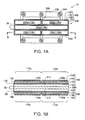
- Fig. 1A is a plan view showing a schematic configuration of a piezoelectric driving device 10 in a first embodiment of the invention
- Fig. 1B is a sectional view along line B-B thereof.
- the piezoelectric driving device 10 includes a vibrating plate 200 and two piezoelectric vibrators 100 respectively provided on both surfaces of the vibrating plate 200 (a first surface 211 (also referred to as "front surface") and a second surface 212 (also referred to as "rear surface”)).
- the piezoelectric vibrator 100 includes a substrate 120, a first electrode 130 formed on the substrate 120, a piezoelectric body 140 formed on the first electrode 130, and a second electrode 150 formed on the piezoelectric body 140.
- the first electrode 130 and the second electrode 150 sandwich the piezoelectric body 140.
- the two piezoelectric vibrators 100 are symmetrically provided with respect to the vibrating plate 200.
- the two piezoelectric vibrators 100 have the same configuration, and the configuration of the piezoelectric vibrator 100 on the upper side of the vibrating plate 200 will be explained unless otherwise noted.
- the substrate 120 of the piezoelectric vibrator 100 is used as a substrate for formation of the first electrode 130, the piezoelectric body 140, and the second electrode 150 in a deposition process. Further, the substrate 120 also has a function as a vibrating plate that mechanically vibrates.
- the substrate 120 may be formed using e.g. Si, Al 2 O 3 , ZrO 2 , or the like.
- As an Si substrate 120 e.g. an Si wafer for semiconductor manufacture can be used.
- the planar shape of the substrate 120 is a rectangular shape.
- the thickness of the substrate 120 is preferably e.g. in a range from 10 ⁇ m to 100 ⁇ m.
- the substrate 120 When the thickness of the substrate 120 is set to 10 ⁇ m or more, the substrate 120 may be handled relatively easily in deposition processing on the substrate 120. Note that, when the thickness of the substrate 120 is set to 50 ⁇ m or more, the substrate 120 may be handled more easily. Or, when the thickness of the substrate 120 is set to 100 ⁇ m or less, the substrate 120 may be vibrated easily in response to expansion and contraction of the piezoelectric body 140 formed by a thin film.
- the first electrode 130 is formed as a single continuous conductor layer formed on the substrate 120.
- the second electrode 150 is sectioned into five conductor layers 150a to 150e (also referred to as "second electrodes 150a to 150e") as shown in Fig. 1A .
- the second electrode 150e at the center is formed in a rectangular shape over nearly the entire in the longitudinal direction of the substrate 120 at the center in the width direction (lateral direction) of the substrate 120.
- the other four second electrodes 150a, 150b, 150c, 150d have the same planar shape and are formed in the positions in the four corners of the substrate 120.
- both the first electrode 130 and the second electrode 150 have rectangular planar shapes.
- the first electrode 130 and the second electrode 150 are thin films formed by e.g. sputtering.
- materials for the first electrode 130 and the second electrode 150 arbitrary materials having higher conductivity, e.g., Al (aluminum), Ni (nickel), Au (gold), Pt (platinum), Ir (iridium) are available. Note that, instead of using a single continuous conductor layer for the first electrode 130, the first electrode may be sectioned into five conductor layers having substantially the same planar shapes as the second electrodes 150a to 150e.
- wiring for electrical connection among the second electrodes 150a to 150e and wiring (or a wiring layer and an insulating layer) for electrical connection among the first electrode 130 and the second electrodes 150a to 150e and the drive circuit are not shown in Figs. 1A and 1B .
- the piezoelectric body 140 is formed as five piezoelectric body layers having substantially the same planar shapes as the second electrodes 150a to 150e. Instead, the piezoelectric body 140 may be formed as a single continuous piezoelectric body layer having substantially the same planar shape as the first electrode 130. Five piezoelectric elements 110a to 110e ( Fig. 1A ) are formed by the layered structure of the first electrode 130, piezoelectric body 140, and the second electrodes 150a to 150e.
- the piezoelectric body 140 is a thin film formed by e.g. the sol-gel method or sputtering method.
- As the material for the piezoelectric body 140 an arbitrary material that exhibits the piezoelectric effect including ceramics having an ABO 3 -type perovskite structure is available.
- As the ceramics having the ABO 3 -type perovskite structure e.g.
- PZT lead zirconate titanate
- BST barium strontium titanate
- SBT strontium bismuth tantalate
- lead metaniobate lead zinc niobate, lead scandium niobate, or the like
- another material exhibiting the piezoelectric effect than ceramics e.g., polyvinylidene fluoride, crystal, or the like can be used. It is preferable that the thickness of the piezoelectric body 140 is set e.g. within a range from 50 nm (0.05 ⁇ m) to 20 ⁇ m.
- the thin film of the piezoelectric body 140 having the thickness within the range may be easily formed using a deposition process.
- the thickness of the piezoelectric body 140 is set to 0.05 ⁇ m or more, a sufficiently large force may be generated in response to the expansion and contraction of the piezoelectric body 140.
- the piezoelectric driving device 10 may be sufficiently downsized.
- Fig. 2 is a plan view of the vibrating plate 200.
- the vibrating plate 200 has a vibrator part 210 having a rectangular shape and three connecting portions 220 respectively extending from the right and left longitudinal sides of the vibrator part 210, and two attachment portions 230 respectively connected to the right and left three connecting portions 220. Note that, in Fig. 2 , for convenience of illustration, the vibrator part 210 is hatched.
- the attachment portions 230 are used for attaching the piezoelectric driving device 10 to another member using screws 240.
- the vibrating plate 200 can be formed using a metal material, e.g., stainless steel, aluminum, aluminum alloy, titanium, titan alloy, copper, copper alloy, iron-nickel alloy, or the like.
- the length L of the vibrator part 210 may be set e.g. in a range from 3.5 mm to 30 mm and the width W may be set e.g. in a range from 1 mm to 8 mm.
- the thickness of the vibrator part 210 (the thickness of the vibrating plate 200) may be set e.g. in a range from 50 ⁇ m to 700 ⁇ m.
- the thickness of the vibrator part 210 is set to 50 ⁇ m or more, the part has sufficient rigidity for supporting the piezoelectric vibrators 100.
- the thickness of the vibrator part 210 is set to 700 ⁇ m or less, the part may generate sufficiently large deformation in response to the deformation of the piezoelectric vibrators 100.
- a projecting portion 20 (also referred to as “contact portion” or “acting portion”) is provided on one short side of the vibrating plate 200.
- the projecting portion 20 is a member that comes into contact with a driven member and provides force to the driven member. It is preferable to form the projecting portion 20 using a material having durability such as ceramics (e.g. Al 2 O 3 ).
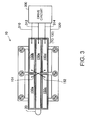
- Fig. 3 is an explanatory diagram showing an electrical connection state between the piezoelectric driving device 10 and a drive circuit 300.
- the five second electrodes 150a to 150e one diagonal pair of second electrodes 150a, 150d are electrically connected to each other via a line 151 and the other diagonal pair of second electrodes 150b, 150c are electrically connected to each other via a line 152.
- These wires 151, 152 may be formed by deposition processing or implemented by wire-shaped lines.
- Three second electrodes 150b, 150e, 150d on the right side of Fig. 3 and the first electrode 130 ( Figs. 1A and 1B ) are electrically connected to the drive circuit 300 via lines 310, 312, 314, 320.
- the drive circuit 300 can ultrasonically vibrate the piezoelectric driving device 10 and rotate the rotor (driven member) in contact with the projecting portion 20 in a predetermined rotation direction by applying a periodically changing alternating-current voltage or undulating voltage between the one pair of second electrodes 150a, 150d and the first electrode 130.
- undulating voltage refers to a voltage formed by addition of a DC offset to an alternating-current voltage, the direction of the voltage (electric field) is one direction from one electrode to the other electrode.
- the circuit can rotate the rotor in contact with the projecting portion 20 in the opposite direction by applying an alternating-current voltage or undulating voltage between the other pair of second electrodes 150b, 150c and the first electrode 130.
- the voltage application is performed at the same time on the two piezoelectric vibrators 100 provided on the surfaces of the vibrating plate 200.
- the wiring (or the wiring layer and the insulating layer) forming the lines 151, 152, 310, 312, 314, 320 shown in Fig. 3 is not shown in Figs. 1A and 1B .
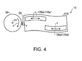
- Fig. 4 is an explanatory diagram showing an example of a movement of the piezoelectric driving device 10.
- the projecting portion 20 of the piezoelectric driving device 10 is in contact with the outer circumference of a rotor 50 as a driven member.
- the drive circuit 300 applies the alternating-current voltage or undulating voltage between the one pair of second electrodes 150a, 150d and the first electrode 130, and the piezoelectric elements 110a, 110d expand and contract in directions of arrows x in Fig. 4 .
- the vibrator part 210 of the piezoelectric driving device 10 is bended within the plane of the vibrator part 210 and deformed into a meandering shape (S-shape), and the end of the projecting portion 20 performs reciprocating motion in the directions of arrows y or elliptic motion.
- the rotor 50 rotates about its center 51 in a predetermined direction z (clockwise direction in Fig. 4 ).
- the three connecting portions 220 ( Fig. 2 ) of the vibrating plate 200 explained in Fig. 2 are provided in positions of nodes of the vibration of the vibrator part 210.
- the drive circuit 300 applies the alternating-current voltage or undulating voltage between the other pair of second electrodes 150b, 150c and the first electrode 130, the rotor 50 rotates in the opposite direction. If the same voltage as that to the one pair of second electrodes 150a, 150d (or the other pair of second electrodes 150b, 150c) is applied to the second electrode 150e at the center, the piezoelectric driving device 10 expands and contracts in the longitudinal directions, and the force provided from the projecting portion 20 to the rotor 50 can be made larger. Note that the movement of the piezoelectric driving device 10 (or piezoelectric vibrator 100) is disclosed in the related art document ( JP-A-2004-320979 or the counterpart U.S. Patent No. 7224102 ), and the disclosed contents are incorporated herein by reference.
- Fig. 5 is a sectional view of the example of the sectional structure shown in Fig. 1B further in detail.
- the piezoelectric vibrator 100 includes the substrate 120, an insulating layer 125, the first electrode 130, the piezoelectric body 140, the second electrodes 150, an insulating layer 160, and lead electrodes 171, 172.
- the plurality of second electrodes 150 and the plurality of lead electrodes 171, 172 are distinguished by addition of an index "c" or "d".
- the lines 151, 152 shown in Fig. 3 are not shown.
- the insulating layer 125 is formed on the substrate 120 and insulates between the substrate 120 and the first electrode 130.
- the first electrode 130 is formed on the insulating layer 125.
- the piezoelectric body 140 is formed on the first electrode 130.
- the second electrode 150 is formed on the piezoelectric body 140.
- the insulating layer 160 is formed on the second electrode 150. Further, the insulating layer 160 has openings (contact holes) in its parts for the first lead electrode 171 into contact with the first electrode 130 and the second lead electrode 172 into contact with the second electrode 150.
- the first lead electrode 171 is formed on the insulating layer 160 and in contact with the first electrode 130.
- the second lead electrode 172 is formed on the insulating layer 160 and in contact with the second electrode 150.
- the two lead electrodes 171, 172 are not directly connected to each other.
- the second lead electrodes 172c, 172d are formed in positions closer to the boundary between the piezoelectric element 110c and the piezoelectric element 110d, however, the second lead electrodes 172c, 172d may be formed on both ends in the longitudinal direction of the vibrating plate 200 on the opposite sides to the boundary between the piezoelectric element 110c and the piezoelectric element 110d. In this case, when the positions of the first lead electrodes 171c, 171d and the second lead electrodes 172c, 172d in the width direction (in the lateral direction of the vibrating plate 200) are different, they are not connected to each other.
- the second lead electrodes 172c, 172d may extend to regions without the piezoelectric body 140 underneath. If the lines 151, 152, 314 are connected to the second lead electrodes 172 in the regions without the piezoelectric body 140 underneath, electrostatic breakdown of the piezoelectric body 140 due to wiring connection is harder to occur.
- Fig. 6 is an explanatory diagram showing a manufacturing flowchart of the piezoelectric driving device 10.
- the piezoelectric element 110 is formed on the substrate 120, and thereby, the piezoelectric vibrator 100 is formed.
- the substrate 120 e.g. an Si wafer may be used as the substrate 120.
- a plurality of the piezoelectric vibrators 100 can be formed on the single Si wafer.
- Si has a value of mechanical quality factor Qm as large as about a hundred thousand, and the mechanical quality factors Qm of the piezoelectric vibrators 100 and the piezoelectric driving device 10 may be made larger.
- the substrate 120 with the piezoelectric driving devices 10 formed thereon are diced and divided into individual piezoelectric vibrators 100.
- the rear surface of the substrate 120 may be ground so that the substrate 120 may have a desired thickness.
- the two piezoelectric vibrators 100 are bonded to the surfaces of the vibrating plate 200 using adhesive agents.
- the wiring layers of the piezoelectric vibrators 100 and the drive circuit are electrically connected by wiring.
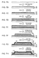
- Figs. 7A to 7H are explanatory diagrams showing a manufacturing process of the piezoelectric vibrator 100 at step S100 in Fig. 6 .
- Figs. 7A to 7H show a process of forming the piezoelectric element 110d shown in the upper part of the right half of Fig. 5 .
- the substrate 120 is prepared and the insulating layer 125 is formed on the front surface of the substrate 120.
- the insulating layer 125 e.g. an SiO 2 layer formed by thermal oxidation of the front surface of the substrate 120 may be used.
- alumina (Al 2 O 3 ) or an organic material such as acryl or polyimide may be used for the insulating layer. Note that, when the substrate 120 is an insulator, the step of forming the insulating layer 125 may be omitted.
- the first electrode 130 is formed on the insulating layer 125.
- the first electrode 130 may be formed by e.g. sputtering.
- the piezoelectric body 140 is formed on the first electrode 130.
- the piezoelectric body 140 can be formed using e.g. the sol-gel method. That is, a sol-gel solution of a piezoelectric body material is dropped on the substrate 120 (first electrode 130), the substrate 120 is rotated at a high speed, and thereby, a thin film of the sol-gel solution is formed on the first electrode 130. Then, preliminary calcination is performed at a temperature of 200 to 300°C and a first layer of the piezoelectric material is formed on the first electrode 130.
- the piezoelectric body layer is formed to a desired thickness on the first electrode 130.
- the thickness of one layer of the piezoelectric body formed in one cycle is a thickness of about 50 nm to 150 nm, though depending on the viscosity of the sol-gel solution and the rotation speed of the substrate 120.
- the piezoelectric body layer is formed to the desired thickness, then, sintered at a temperature of 600°C to 1000°C, and thereby, the piezoelectric body 140 is formed.
- the thinner piezoelectric driving device 10 When the thickness of the sintered piezoelectric body 140 is set to be from 50 nm (0.05 ⁇ m) to 20 ⁇ m, the smaller piezoelectric driving device 10 may be implemented. Note that, when the thickness of the piezoelectric body 140 is set to 0. 05 ⁇ m or more, a sufficiently large force may be generated in response to the expansion and contraction of the piezoelectric body 140. Further, when the thickness of the piezoelectric body 140 is set to 20 ⁇ m or less, a sufficiently large force may be generated even when the voltage applied to the piezoelectric body 140 is equal to or less than 600 V. As a result, the drive circuit 300 for driving the piezoelectric driving device 10 may be formed using inexpensive elements.
- the thickness of the piezoelectric body 140 may be set to 400 nm or more, and, in this case, the force generated in the piezoelectric element may be increased.
- the temperatures and periods for the preliminary calcination and sintering are just examples and appropriately selected depending on the piezoelectric body material.
- the thin film of the piezoelectric body material is formed using the so-gel method and sintered, there are advantages that (a) the thin film is formed more easily, (b) crystallization with oriented lattice direction is performed more easily, and (c) the withstand voltage of the piezoelectric body may be improved compared to the sintering method of mixing and sintering raw material powder in related art.
- the second electrode 150 is formed on the piezoelectric body 140.
- the formation of the second electrode 150 may be performed by sputtering like the first electrode.
- the second electrode 150 and the piezoelectric body 140 are patterned.
- patterning of the second electrode 150 and the piezoelectric body 140 is performed by ion milling using an argon ion beam. Note that the period for ion milling is controlled, and thereby, only patterning of the second electrode 150 and the piezoelectric body 140 except the first electrode 130 can be performed. Note that, in place of patterning using ion milling, patterning may be performed by another arbitrary patterning method (e.g. dry etching using chlorine-containing gas).
- the insulating layer 160 is formed on the first electrode 130 and the second electrode 150.
- a phosphorus-containing silicon oxide film PSG film
- a boron phosphorus-containing silicon oxide film BPSG film
- an NSG film silicon oxide film containing no impurities such as boron or phosphorus
- Si 3 N 4 film silicon nitride film
- a conductor layer for lead electrodes is formed and patterned.
- the conductor layer may be formed using e.g. aluminum and formed by sputtering. Then, the conductor layer is patterned, and thereby, the first lead electrode 171 and the second lead electrode 172 are formed.
- the first lead electrode 171 is connected to the first electrode 130 and the second lead electrode 172 is connected to the second electrode 150. Note that, when the first electrodes 130 of the piezoelectric elements 110a to 110e form a single continuous conductor layer, the second lead electrodes 172 are not necessarily formed in the other piezoelectric elements 110a, 110b, 110c, 110e.
- the second lead electrode 172 may extend to a region without the piezoelectric body 140 underneath.
- both the first lead electrode 171 and the second lead electrode 172 may be left on the insulating layer 160.
- the wiring layer of the vibrating plate 200 and the first lead electrode 171, the second lead electrode 172 may be electrically connected more easily.
- a passivation film is formed on the first lead electrode 171 and the second lead electrode 172.
- the passivation film may be formed using e.g. SiN, polyimide.
- opening portions (contact holes) for connection of the first lead electrodes 171 and the second lead electrodes 172 to the lines 151, 152, 310, 312, 314, 320 ( Fig. 3 ) are formed.
- Figs. 8A and 8B are explanatory diagram showing an example of wiring between the piezoelectric driving device 10 and the drive circuit 300.
- the connection states of wiring on the front surface side and the rear surface side of the piezoelectric driving device 10 are shown.
- the sizes of the electrodes 150a to 150e etc. are different from those in Figs. 1A and 1B .
- the second electrodes 150a, 150b, 150c, 150d, 150e, the first lead electrodes 171a, 171b, 171c, 171d, 171e, and the second lead electrodes 172a, 172b, 172c, 172d, 172e are respectively provided on the front surface and the rear surface of the piezoelectric driving device.
- indices a, b, c, d, e are added to the ends of the second electrodes 150, the first lead electrodes 171, and the second lead electrodes 172.
- the first electrode 130 forms a single continuous conductor layer
- the first lead electrodes 171a, 171b, 171c, 171d, 171e shown by broken lines in Figs. 8A and 8B are not necessarily formed.
- the lines connecting the respective electrodes of the piezoelectric driving device 10 are wired as follows.
- the respective electrodes of the piezoelectric driving device 10 and the drive circuit are connected as follows.
- the piezoelectric elements 110b, 110c may be driven.
- the piezoelectric elements 110a, 110d may be driven.
- the piezoelectric element 110e may be driven.
- the thickness of the piezoelectric body 140 is set to be from 50 nm (0.05 ⁇ m) to 20 ⁇ m, and thereby, the smaller piezoelectric driving device 10 may be implemented.
- the thickness of the piezoelectric body 140 is set to 0.05 ⁇ m or more, a sufficiently large force may be generated in response to the expansion and contraction of the piezoelectric body 140.
- the thickness of the piezoelectric body 140 is set to 20 ⁇ m or less, a sufficiently large force may be generated even when the voltage applied to the piezoelectric body 140 is equal to or less than 600 V. Therefore, the drive circuit 300 for driving the piezoelectric driving device 10 may be formed using inexpensive elements.
- the voltage actually applied to the piezoelectric body 140 is sufficient in a range from 20 to 40 V.
- the thickness of the piezoelectric body may be set to 400 nm or more, and, in this case, the force generated in the piezoelectric element may be increased.
- the piezoelectric elements (110a to 110e) are formed on the substrate 120, and thereby, the value of mechanical quality factor Qm of the piezoelectric driving device 10 may be made larger than that of the case without the substrate 120.
- the mechanical quality factor Qm value of the Si substrate is about a hundred thousand, and, when the Si substrate 120 is used, the value of mechanical quality factor Qm of the piezoelectric driving device 10 may be made larger.
- the piezoelectric vibrator 100 has the substrate 120, the first electrode 130 provided on the substrate 120, the piezoelectric body 140 provided on the first electrode 130, and the second electrode 150 provided on the piezoelectric body 140, and thereby, even when the thickness of the piezoelectric body 140 is made thinner, the mechanical strength and the mechanical quality factor Qm of the piezoelectric vibrator 100 may be made larger.
- the silicon substrate is used as the substrate 120.
- the value of the mechanical quality factor Qm of the piezoelectric body 140 is several thousands and, in contrast, the value of the mechanical quality factor Qm of the substrate 120 is about a hundred thousand. Therefore, the value of the mechanical quality factor Qm of the piezoelectric driving device 10 may be made larger.
- the thickness of the substrate 120 may be from 10 ⁇ m to 100 ⁇ m.
- the substrate 120 may be handled relatively easily in deposition processing on the substrate 120.
- the substrate 120 may be vibrated easily in response to expansion and contraction of the piezoelectric body 140 formed by a thin film.
- the piezoelectric vibrator 100 has the insulating layer 160 on the second electrode 150, and the first lead electrode 171 connected to the first electrode 130 and the second lead electrode 172 connected to the second electrode 150 on the insulating layer 160, and thereby, the lines 151, 152, 310, 312, 314, 320 may be wired to the first lead electrode 171, the second lead electrode 172 and voltages may be applied from the first lead electrode 171, the second lead electrode 172. Further, compared to the case of direct wiring to the first electrode 130, the second electrode 150, electrostatic breakdown of the piezoelectric body 140 or the like is harder to occur when the wiring is connected and leakage current of the piezoelectric body 140 may be suppressed.
- the piezoelectric body 140 it is preferable to form the piezoelectric body 140 by the sol-gel method because the thinner piezoelectric body is easily formed. Further, it is preferable to easily orient the lattice direction of the crystal of the piezoelectric body because deformation of the shape of the piezoelectric body may be made larger when the same voltage is applied and the withstand voltage may be made larger. Note that the piezoelectric body 140 may be formed by the sputtering method. The same advantage as that by the sol-gel method may be obtained by the sputtering method.
- Fig. 9 is a sectional view of a piezoelectric driving device 10a as another embodiment of the invention, and corresponds to Fig. 1B of the first embodiment.
- the piezoelectric vibrator 100 is provided upside down to that in Fig. 1B on the vibrating plate 200. That is, here, the vibrator is provided so that the second electrode 150 may be closer to the vibrating plate 200 and the substrate 120 may be farthest from the vibrating plate 200.
- the vibrator is provided so that the second electrode 150 may be closer to the vibrating plate 200 and the substrate 120 may be farthest from the vibrating plate 200.
- the piezoelectric driving device 10a may also achieve the same effect as that of the first embodiment.
- Figs. 10A to 10E are explanatory diagrams showing a manufacturing process of the piezoelectric driving device 10a shown in Fig. 9 .
- the vibrating plate 200 is prepared and insulating layers 202 are formed.
- the insulating layers 202 can be formed using e.g. an insulating resin such as polyimide.
- wiring layers 204 are formed on the insulating layers 202 and the wiring layers 204 are patterned.
- the wiring layers 204 include first wiring and second wiring.
- copper or aluminum may be used.
- insulating layers 206 are formed on the wiring layers 204 and opening portions are patterned.
- the insulating layers 206 may be formed using e.g. solder resists.
- the piezoelectric vibrators 100 individually formed by the step S200 in Fig. 6 are bonded to both surfaces of the vibrating plate 200.
- conducting members 208 are provided between the wiring layers 204 and the first lead electrodes 171, the second lead electrodes 172 for electrical contact via the conducting members 208.
- the first wiring of the wiring layer 204 and the first lead electrode 171 are brought into electrical contact and the second wiring of the wiring layer 204 and the second lead electrode 172 are brought into electrical contact.
- the conducting members 208 By intervention of the conducting members 208, even when there are steps between the wiring layers 204 of the vibrating plate 200 and the first lead electrodes 171 and the second lead electrodes 172 of the piezoelectric vibrators 100, the steps may be relaxed for electrical contact.
- the conducting members 208 e.g. micro bumps or conducting paste may be used.
- the first surface side in Fig. 10E shows a state in which the piezoelectric vibrator 100 has been bonded and the second surface side shows a state immediately before bonding of the piezoelectric vibrator 100. Note that the above described passivation films 180 are formed in the upper parts of the piezoelectric vibrators 100 shown in Fig. 10E .
- the passivation films 180 protect around the first lead electrodes 171, the second lead electrodes 172 and suppress electrical short circuit between the first lead electrodes 171, the second lead electrodes 172 and the other members.
- the shape of the second lead electrode 172 is extended to a region without the piezoelectric body 140 underneath, however, it is not necessarily extended. This is because the second lead electrode 172 is connected to the wiring layer 204 of the vibrating plate 200 via the conducting member 208 and it is not necessary to extend the electrode to the region without the piezoelectric body 140 underneath.
- the wiring layers 204 and the drive circuit 300 are connected by the lines 310, 312, 314, 320. That is, in the embodiment, the lines 310, 312, 314, 320 are not directly wired to the first lead electrodes 171, the second lead electrode 172, but wired via the wiring layers 204. Accordingly, direct wiring to the vibrating piezoelectric vibrators 100 is not necessary and, even when the piezoelectric vibrators 100 vibrate, detachment of the wiring is harder.
- the lines 310, 312, 314, 320 are connected after the piezoelectric vibrators 100 are bonded to the vibrating plate 200, however, the lines 310, 312, 314, 320 may be first connected, and then, the piezoelectric vibrators 100 may be bonded to the vibrating plate 200.
- Fig. 11A is a plan view of a piezoelectric driving device 10b as yet another embodiment of the invention and corresponds to Fig. 1A of the first embodiment.
- the connecting portions 220 and the attachment portions 230 of the vibrating plate 200 are not shown.
- a pair of second electrodes 150b, 150c are omitted.
- the piezoelectric driving device 10b can also rotate the rotor 50 in one direction z as shown in Fig. 4 . Note that the same voltage is applied to the three second electrodes 150a, 150e, 150d in Fig. 11A , and the three second electrodes 150a, 150e, 150d may be formed as a single continuous electrode layer.
- Fig. 11B is a plan view of a piezoelectric driving device 10c as yet another embodiment of the invention.
- the second electrode 150e at the center in Fig. 1A is omitted and the other four second electrodes 150a, 150b, 150c, 150d are formed in larger areas than those in Fig. 1A .
- the piezoelectric driving device 10c also may achieve nearly the same effect as that of the first embodiment.
- Fig. 11C is a plan view of a piezoelectric driving device 10d as yet another embodiment of the invention.
- the four second electrodes 150a, 150b, 150c, 150d in Fig. 1A are omitted and one second electrode 150e is formed in a larger area.
- the piezoelectric driving device 10d only expands and contracts in the longitudinal directions, but can provide a larger force to the driven member (not shown) from the projecting portion 20.
- the second electrode 150 of the piezoelectric vibrator 100 at least one electrode layer may be provided. Note that, as in the embodiments shown in Figs. 1A and 1B and Figs. 11A to 11B , it is preferable to provide the second electrodes 150 in diagonal positions of the rectangular piezoelectric vibrator 100 because the piezoelectric vibrator 100 and the vibrating plate 200 can be deformed to bend into a meandering shape within the plane.
- the above described piezoelectric driving device 10 may provide a larger force to a driven member using resonance, and can be applied to various apparatuses.
- the piezoelectric driving device 10 may be used as a driving device in various apparatuses including e.g. a robot (including an electronic part carrying apparatus (IC handler)), a chemical dosing pump, a calendar advancing apparatus of a clock, and a printing apparatus (e.g. a paper feed mechanism, though not applied to a head because the vibrating plate is not resonated in a piezoelectric driving device used for the head).
- a robot including an electronic part carrying apparatus (IC handler)
- a chemical dosing pump e.g. a chemical dosing pump
- a calendar advancing apparatus of a clock e.g. a calendar advancing apparatus of a clock
- a printing apparatus e.g. a paper feed mechanism, though not applied to a head because the vibrating plate is not resonated in a piezoelectric driving device used for the head
- Fig. 12 is an explanatory diagram showing an example of a robot 2050 using the above described piezoelectric driving devices 10.
- the robot 2050 has an arm 2010 (also referred to as "arm part") including a plurality of link parts 2012 (also referred to as “link members”) and a plurality of joint parts 2020 rotatably or bendably connecting between the link parts 2012.
- Each joint part 2020 contains the above described piezoelectric driving devices 10 and can rotate or bend the joint part 2020 to an arbitrary angle using the piezoelectric driving device 10.
- a robot hand 2000 is connected to the distal end of the arm 2010.
- the robot hand 2000 includes a pair of grasping parts 2003.
- the robot hand 2000 also contains the piezoelectric driving device 10 and can grasp an object by opening and closing the grasping parts 2003 using the piezoelectric driving device 10. Further, the piezoelectric driving device 10 is also provided between the robot hand 2000 and the arm 2010 and can rotate the robot hand 2000 with respect to the arm 2010 using the piezoelectric driving device 10.
- Fig. 13 is an explanatory diagram of a wrist part of the robot 2050 shown in Fig. 12 .
- the joint parts 2020 sandwich a wrist rotating part 2022 and the link part 2012 of the wrist is rotatably attached about the center axis O of the wrist rotating part 2022.
- the wrist rotating part 2022 contains the piezoelectric driving device 10 and the piezoelectric driving device 10 rotates the link part 2012 of the wrist and the robot hand 2000 about the center axis O.
- the plurality of grasping parts 2003 are stood.
- the base end parts of the grasping parts 2003 are movable within the robot hand 2000 and the piezoelectric driving devices 10 are provided in the base parts of the grasping parts 2003. Accordingly, the piezoelectric driving devices 10 are operated, and thereby, the grasping parts 2003 may be moved to grasp an object.
- the piezoelectric driving device 10 may be applied not only to a single-arm robot but also to a multi-arm robot having two or more arms.
- the joint parts 2020 of the wrist and the robot hand 2000 contain not only the piezoelectric driving devices 10 but also power lines for supplying power to various devices including force sensors and gyro sensors, signal lines for transmitting signals, etc. , and lots of wiring is necessary. Therefore, it was very difficult to provide wiring within the joint parts 2020 and the robot hand 2000.
- a drive current may be made smaller than in a general electric motor or a piezoelectric driving device in related art, and thus, wiring can be provided even in the smaller spaces in the joint parts 2020 (specifically, the joint parts of the distal end of the arm 2010) and the robot hand 2000.
- Fig. 14 is an explanatory diagram showing an example of a liquid delivery pump 2200 using the above described piezoelectric driving device 10.
- a reservoir 2211, a tube 2212, the piezoelectric driving device 10, a rotor 2222, a reduction transmission mechanism 2223, a cam 2202, and a plurality of fingers 2213, 2214, 2215, 2216, 2217, 2218, 2219 are provided within a case 2230.
- the reservoir 2211 is a container part for housing a liquid to be carried.
- the tube 2212 is a tube for carrying the liquid output from the reservoir 2211.
- the projecting portion 20 of the piezoelectric driving device 10 is provided in press contact with the side surface of the rotor 2222 and the piezoelectric driving device 10 rotationally drives the rotor 2222.
- the rotation force of the rotor 2222 is transmitted to the cam 2202 via the reduction transmission mechanism 2223.
- the fingers 2213 to 2219 are members for blocking the tube 2212. When the cam 2202 rotates, the fingers 2213 to 2219 are sequentially pushed outward in the radial direction by projecting portions 2202A of the cam 2202.
- the fingers 2213 to 2219 block the tube 2212 sequentially from the upstream side in the carrying direction (the reservoir 2212 side). Thereby, the liquid within the tube 2212 is sequentially carried to the downstream side.
- the smaller liquid delivery pump 2200 that can deliver an extremely small amount of the liquid with higher accuracy may be implemented.
- the arrangement of the respective members is not limited to the illustrated one.
- a ball or the like provided on the rotor 2222 may block the tube 2212.
- the above described liquid delivery pump 2200 may be utilized for a chemical dosing apparatus for giving a medical solution such as insulin to a human body.
- the piezoelectric driving device 10 of the above described embodiment is used, and thereby, drive currents are smaller than those in the piezoelectric driving device in related art, and power consumption of the chemical dosing apparatus may be suppressed. Therefore, the embodiment is particularly effective when the chemical dosing apparatus is driven using a battery.
- the first electrode 130, the piezoelectric body 140, and the second electrode 150 are formed on the substrate 120, however, the substrate 120 may be omitted and the first electrode 130, the piezoelectric body 140, and the second electrode 150 may be formed on the vibrating plate 200.
- the respective single piezoelectric vibrators 100 are provided on both surfaces of the vibrating plate 200, however, one of the piezoelectric vibrators 100 may be omitted. Note that it is preferable to respectively provide the piezoelectric vibrators 100 on both surfaces of the vibrating plate 200 because the vibrating plate 200 is deformed to bend in a meandering shape within the plane more easily.
Abstract

Description
- The present invention relates to a piezoelectric driving device and a driving method therefor, and a robot and a driving method therefor.
- Piezoelectric actuators (piezoelectric driving devices) that drive driven members by vibrating piezoelectric bodies require no magnets or coils and are used in various fields (e.g. Patent Document 1 (
JP-A-2004-320979 JP-A-2008-227123 - In the case where a piezoelectric driving device is housed and used in a small space (e.g. within a joint of a robot), the wiring space may be insufficient with a piezoelectric driving device using a piezoelectric body of related art, and there has been a demand for a thinner piezoelectric body. However, if the piezoelectric body is made too much thinner, the force generated in the piezoelectric element becomes extremely small and displacement necessary for driving of the driven member is not obtained, and thus, it is necessary to increase the mechanical quality factor Qm for increasing the displacement. Further, it is necessary to suppress heat generation for housing of the piezoelectric driving device in the small space, and it is necessary to reduce mechanical loss with vibrations by increasing the mechanical quality factor Qm. As described above, in related art, an appropriate configuration of the small piezoelectric driving device that can drive the driven member is not sufficiently studied.
- The object of the invention is to solve at least a part of the problems described above, and the invention can be implemented as the following forms or application examples.
- (1) An aspect of the invention provides a piezoelectric driving device. The piezoelectric driving device includes a vibrating plate, and a piezoelectric vibrator having a first electrode, a second electrode, and a piezoelectric body located between the first electrode and the second electrode and provided on the vibrating plate, wherein a thickness of the piezoelectric body is from 50 nm to 20 µm. According to this configuration, the thickness of the piezoelectric body is set to be from 50 nm (0.05 µm) to 20 µm, and the smaller piezoelectric driving device may be implemented.
- (2) In the piezoelectric driving device according to the aspect, the thickness of the piezoelectric body may be from 400 nm to 20 µm. According to this configuration, the thickness of the piezoelectric body is set to 400 nm or more, a force generated in a piezoelectric element may be made larger.
- (3) In the piezoelectric driving device according to the aspect, the piezoelectric vibrator may have a substrate, the first electrode formed on the substrate, the piezoelectric body formed on the first electrode, and the second electrode formed on the piezoelectric body, and the substrate may be bonded to the vibrating plate. In order to extract higher energy from the piezoelectric element, the mechanical quality factor Qm may be made larger so that a larger amplitude may be obtained in the resonance state. According to this configuration, the piezoelectric body, the first electrode, and the second electrode are formed on the substrate, and thereby, the value of the mechanical quality factor Qm of the piezoelectric driving device may be made larger than that of the case without the substrate.
- (4) In the piezoelectric driving device according to the aspect, the substrate may be a silicon substrate. The value of the mechanical quality factor Qm of the piezoelectric body is several thousands and, in contrast, the value of the mechanical quality factor Qm of the silicon substrate is about a hundred thousand. Therefore, according to this configuration, the value of the mechanical quality factor Qm of the piezoelectric driving device may be made larger.
- (5) In the piezoelectric driving device according to the aspect, the vibrating plate may have a first surface and a second surface, and the piezoelectric vibrators may be provided on the first surface and the second surface of the vibrating plate. According to this configuration, the piezoelectric elements are provided on the first surface and the second surface of the vibrating plate, and thereby, a driving force of the piezoelectric driving device may be made larger.
- (6) In the piezoelectric driving device according to the aspect, the vibrating plate may include a projecting portion in contact with a driven member. According to this configuration, the projecting portion may push the driven member to drive the driven member.
- (7) Another aspect of the invention provides a piezoelectric driving device. The piezoelectric driving device includes a vibrating plate and a piezoelectric vibrator provided on the vibrating plate, and the piezoelectric vibrator includes a substrate, a first electrode provided on the substrate, a piezoelectric body provided on the first electrode, and a second electrode provided on the piezoelectric body. According to this configuration, the piezoelectric vibrator includes the substrate, and, even when the piezoelectric body is made thinner, the mechanical strength and the mechanical quality factor Qm of the piezoelectric vibrator may be made larger. As a result, an appropriate configuration of the smaller piezoelectric driving device may be implemented.
- (8) In the piezoelectric driving device according to the aspect, the piezoelectric vibrator may have an insulating layer on the second electrode and a first lead electrode connected to the first electrode and a second lead electrode connected to the second electrode on the insulating layer. According to this configuration, wiring to the first lead electrode, the second lead electrode may be provided and voltages may be applied from the first lead electrode, the second lead electrode. Compared to the case of direct wiring to the first electrode, the second electrode, no piezoelectric body exists under the position of the wiring connection, and electrostatic breakdown of the piezoelectric body or the like is harder to occur when the wiring is connected and leakage current of the piezoelectric body may be suppressed.
- (9) In the piezoelectric driving device according to the aspect, the piezoelectric vibrator may be provided on the vibrating plate so that the second electrode and the vibrating plate may sandwich the piezoelectric body, the first electrode, and the substrate.
- (10) In the piezoelectric driving device according to the aspect, the piezoelectric vibrator may be provided on the vibrating plate so that the substrate and the vibrating plate may sandwich the first electrode, the piezoelectric body, and the second electrode. In the piezoelectric vibrator, the substrate side may be in contact with the vibrating plate or the second electrode side may be in contact with the vibrating plate.
- (11) In the piezoelectric driving device according to the aspect, the vibrating plate may have a wiring layer having a plurality of lines, the piezoelectric vibrator may have an insulating layer on the second electrode, the first lead electrode may be connected to the first line of the plurality of lines, and the second lead electrode may be connected to the second line of the plurality of lines. According to this configuration, wiring to the first line, the second line on the vibrating plate may be provided, and thereby, electrostatic breakdown of the piezoelectric body or the like is harder to occur when the wiring is connected and leakage current of the piezoelectric body may be suppressed.
- (12) In the piezoelectric driving device according to the aspect, the substrate may be a silicon substrate. The value of the mechanical quality factor Qm of the piezoelectric body is several thousands and, in contrast, the value of the mechanical quality factor Qm of the silicon substrate is about a hundred thousand. Therefore, according to this configuration, the value of the mechanical quality factor Qm of the piezoelectric driving device may be made larger.
- (13) In the piezoelectric driving device according to the aspect, a thickness of the substrate may be from 10 µm to 100 µm. When the thickness of the substrate is set to 10 µm or more, the substrate may be handled relatively easily in deposition processing on the substrate. Or, when the thickness of the substrate is set to 100 µm or less, the substrate may be vibrated easily in response to expansion and contraction of the piezoelectric body formed by a thin film.
- (14) In the piezoelectric driving device according to the aspect, the thickness of the substrate may be from 50 nm to 20 µm. When the thickness of the piezoelectric body is set to 50 nm (0.05 µm) or more, a sufficiently large force may be generated in response to the expansion and contraction of the piezoelectric body. Or, when the thickness of the piezoelectric body is set to 20 µm or less, the piezoelectric driving device may be sufficiently downsized.
- (15) In the piezoelectric driving device according to the aspect, the vibrating plate may have a first surface and a second surface, and the piezoelectric vibrators may be provided on the first surface and the second surface of the vibrating plate. According to this configuration, the piezoelectric elements are provided on the first surface and the second surface of the vibrating plate, and thereby, a driving force of the piezoelectric driving device may be made larger.
- (16) In the piezoelectric driving device according to the aspect, the vibrating plate may include a projecting portion in contact with a driven member. According to this configuration, the projecting portion may push the driven member to drive the driven member.
- (17) Still another aspect of the invention provides a robot. The robot includes a plurality of link parts, joint parts connecting the plurality of link parts, and the piezoelectric driving devices according to any one of the above described configurations, which rotate the plurality of link parts in the joint parts. According to this configuration, the piezoelectric driving device may be used for driving of the robot.
- (18) Yet another aspect of the invention provides a driving method for a robot. The driving method includes driving the piezoelectric driving devices by applying periodically changing voltages between the first electrodes and the second electrodes of the piezoelectric driving devices to rotate the plurality of link parts in the joint parts.
- (19) Still yet another aspect of the invention provides a driving method for the piezoelectric driving device. The driving method includes applying, between the first electrode and the second electrode, a periodically changing voltage which is an undulating voltage whose direction of an electric field applied to the piezoelectric body is a single direction from one electrode to the other electrode of the electrodes. According to this configuration, the voltage applied to the piezoelectric body is only in the single direction, and durability of the piezoelectric body may be improved.
- The invention can be implemented in various aspects, and, for example, not only in the piezoelectric driving device but also in various aspects including a driving method for a piezoelectric driving device, a manufacturing method for a piezoelectric driving device, a robot including a piezoelectric driving device, a driving method for a robot including a piezoelectric driving device, a liquid delivery pump, and a chemical dosing pump.
- The invention will be described with reference to the accompanying drawings, wherein like numbers reference like elements.
-
Figs. 1A and 1B are a plan view and a sectional view showing a schematic configuration of a piezoelectric driving device of a first embodiment. -
Fig. 2 is a plan view of a vibrating plate. -
Fig. 3 is an explanatory diagram showing an electrical connection state between the piezoelectric driving device and a drive circuit. -
Fig. 4 is an explanatory diagram showing an example of a movement of the piezoelectric driving device. -
Fig. 5 is a detailed sectional view of the piezoelectric driving device cut along a plane of section in parallel to the longitudinal direction. -
Fig. 6 is a manufacturing flowchart of the piezoelectric driving device. -
Figs. 7A to 7H are explanatory diagrams showing a manufacturing process of a piezoelectric vibrator at step S100 inFig. 6 . -
Figs. 8A and 8B are explanatory diagrams showing an example of wiring between the piezoelectric driving device and the drive circuit. -
Fig. 9 is a sectional view of a piezoelectric driving device as another embodiment of the invention. -
Figs. 10A to 10E are sectional views of the piezoelectric driving device of the other embodiment. -
Figs. 11A to 11C are plan views of piezoelectric driving devices of the other embodiments. -
Fig. 12 is an explanatory diagram showing an example of a robot using the piezoelectric driving devices. -
Fig. 13 is an explanatory diagram of a wrist part of the robot. -
Fig. 14 is an explanatory diagram showing an example of a liquid delivery pump using the piezoelectric driving device. -
Fig. 1A is a plan view showing a schematic configuration of apiezoelectric driving device 10 in a first embodiment of the invention, andFig. 1B is a sectional view along line B-B thereof. Thepiezoelectric driving device 10 includes a vibratingplate 200 and twopiezoelectric vibrators 100 respectively provided on both surfaces of the vibrating plate 200 (a first surface 211 (also referred to as "front surface") and a second surface 212 (also referred to as "rear surface")). Thepiezoelectric vibrator 100 includes asubstrate 120, afirst electrode 130 formed on thesubstrate 120, apiezoelectric body 140 formed on thefirst electrode 130, and asecond electrode 150 formed on thepiezoelectric body 140. Thefirst electrode 130 and thesecond electrode 150 sandwich thepiezoelectric body 140. The twopiezoelectric vibrators 100 are symmetrically provided with respect to the vibratingplate 200. The twopiezoelectric vibrators 100 have the same configuration, and the configuration of thepiezoelectric vibrator 100 on the upper side of the vibratingplate 200 will be explained unless otherwise noted. - The
substrate 120 of thepiezoelectric vibrator 100 is used as a substrate for formation of thefirst electrode 130, thepiezoelectric body 140, and thesecond electrode 150 in a deposition process. Further, thesubstrate 120 also has a function as a vibrating plate that mechanically vibrates. Thesubstrate 120 may be formed using e.g. Si, Al2O3, ZrO2, or the like. As anSi substrate 120, e.g. an Si wafer for semiconductor manufacture can be used. In the embodiment, the planar shape of thesubstrate 120 is a rectangular shape. The thickness of thesubstrate 120 is preferably e.g. in a range from 10 µm to 100 µm. When the thickness of thesubstrate 120 is set to 10 µm or more, thesubstrate 120 may be handled relatively easily in deposition processing on thesubstrate 120. Note that, when the thickness of thesubstrate 120 is set to 50 µm or more, thesubstrate 120 may be handled more easily. Or, when the thickness of thesubstrate 120 is set to 100 µm or less, thesubstrate 120 may be vibrated easily in response to expansion and contraction of thepiezoelectric body 140 formed by a thin film. - The
first electrode 130 is formed as a single continuous conductor layer formed on thesubstrate 120. On the other hand, thesecond electrode 150 is sectioned into fiveconductor layers 150a to 150e (also referred to as "second electrodes 150a to 150e") as shown inFig. 1A . Thesecond electrode 150e at the center is formed in a rectangular shape over nearly the entire in the longitudinal direction of thesubstrate 120 at the center in the width direction (lateral direction) of thesubstrate 120. The other foursecond electrodes substrate 120. In the example ofFigs. 1A and 1B , both thefirst electrode 130 and thesecond electrode 150 have rectangular planar shapes. Thefirst electrode 130 and thesecond electrode 150 are thin films formed by e.g. sputtering. As materials for thefirst electrode 130 and thesecond electrode 150, arbitrary materials having higher conductivity, e.g., Al (aluminum), Ni (nickel), Au (gold), Pt (platinum), Ir (iridium) are available. Note that, instead of using a single continuous conductor layer for thefirst electrode 130, the first electrode may be sectioned into five conductor layers having substantially the same planar shapes as thesecond electrodes 150a to 150e. Also, note that wiring (or a wiring layer and an insulating layer) for electrical connection among thesecond electrodes 150a to 150e and wiring (or a wiring layer and an insulating layer) for electrical connection among thefirst electrode 130 and thesecond electrodes 150a to 150e and the drive circuit are not shown inFigs. 1A and 1B . - The
piezoelectric body 140 is formed as five piezoelectric body layers having substantially the same planar shapes as thesecond electrodes 150a to 150e. Instead, thepiezoelectric body 140 may be formed as a single continuous piezoelectric body layer having substantially the same planar shape as thefirst electrode 130. Fivepiezoelectric elements 110a to 110e (Fig. 1A ) are formed by the layered structure of thefirst electrode 130,piezoelectric body 140, and thesecond electrodes 150a to 150e. - The
piezoelectric body 140 is a thin film formed by e.g. the sol-gel method or sputtering method. As the material for thepiezoelectric body 140, an arbitrary material that exhibits the piezoelectric effect including ceramics having an ABO3-type perovskite structure is available. As the ceramics having the ABO3-type perovskite structure, e.g. lead zirconate titanate (PZT), barium titanate, lead titanate, potassium niobate, lithium niobate, lithium tantalate, sodium tungstate, zinc oxide, barium strontium titanate (BST), strontium bismuth tantalate (SBT), lead metaniobate, lead zinc niobate, lead scandium niobate, or the like can be used. Or, another material exhibiting the piezoelectric effect than ceramics, e.g., polyvinylidene fluoride, crystal, or the like can be used. It is preferable that the thickness of thepiezoelectric body 140 is set e.g. within a range from 50 nm (0.05 µm) to 20 µm. The thin film of thepiezoelectric body 140 having the thickness within the range may be easily formed using a deposition process. When the thickness of thepiezoelectric body 140 is set to 0.05 µm or more, a sufficiently large force may be generated in response to the expansion and contraction of thepiezoelectric body 140. Or, when the thickness of thepiezoelectric body 140 is set to 20 µm or less, thepiezoelectric driving device 10 may be sufficiently downsized. -
Fig. 2 is a plan view of the vibratingplate 200. The vibratingplate 200 has avibrator part 210 having a rectangular shape and three connectingportions 220 respectively extending from the right and left longitudinal sides of thevibrator part 210, and twoattachment portions 230 respectively connected to the right and left three connectingportions 220. Note that, inFig. 2 , for convenience of illustration, thevibrator part 210 is hatched. Theattachment portions 230 are used for attaching thepiezoelectric driving device 10 to another member using screws 240. The vibratingplate 200 can be formed using a metal material, e.g., stainless steel, aluminum, aluminum alloy, titanium, titan alloy, copper, copper alloy, iron-nickel alloy, or the like. - The piezoelectric vibrators 100 (
Figs. 1A and 1B ) are respectively bonded to the upper surface (first surface) and the lower surface (second surface) of thevibrator part 210 using adhesive agents. It is preferable that the ratio between the length L and the width W of thevibrator part 210 is set to nearly L:W = 7:2. This ratio is a preferable value for thevibrator part 210 to perform ultrasonic vibration (to be described later) of bending to right and left along the plane. The length L of thevibrator part 210 may be set e.g. in a range from 3.5 mm to 30 mm and the width W may be set e.g. in a range from 1 mm to 8 mm. Note that it is preferable to set the length L to 50 mm or less for ultrasonic vibration of thevibrator part 210. The thickness of the vibrator part 210 (the thickness of the vibrating plate 200) may be set e.g. in a range from 50 µm to 700 µm. When the thickness of thevibrator part 210 is set to 50 µm or more, the part has sufficient rigidity for supporting thepiezoelectric vibrators 100. Or, when the thickness of thevibrator part 210 is set to 700 µm or less, the part may generate sufficiently large deformation in response to the deformation of thepiezoelectric vibrators 100. - A projecting portion 20 (also referred to as "contact portion" or "acting portion") is provided on one short side of the vibrating
plate 200. The projectingportion 20 is a member that comes into contact with a driven member and provides force to the driven member. It is preferable to form the projectingportion 20 using a material having durability such as ceramics (e.g. Al2O3). -
Fig. 3 is an explanatory diagram showing an electrical connection state between thepiezoelectric driving device 10 and adrive circuit 300. Of the fivesecond electrodes 150a to 150e, one diagonal pair ofsecond electrodes line 151 and the other diagonal pair ofsecond electrodes line 152. Thesewires second electrodes Fig. 3 and the first electrode 130 (Figs. 1A and 1B ) are electrically connected to thedrive circuit 300 vialines drive circuit 300 can ultrasonically vibrate thepiezoelectric driving device 10 and rotate the rotor (driven member) in contact with the projectingportion 20 in a predetermined rotation direction by applying a periodically changing alternating-current voltage or undulating voltage between the one pair ofsecond electrodes first electrode 130. Here, "undulating voltage" refers to a voltage formed by addition of a DC offset to an alternating-current voltage, the direction of the voltage (electric field) is one direction from one electrode to the other electrode. Further, the circuit can rotate the rotor in contact with the projectingportion 20 in the opposite direction by applying an alternating-current voltage or undulating voltage between the other pair ofsecond electrodes first electrode 130. The voltage application is performed at the same time on the twopiezoelectric vibrators 100 provided on the surfaces of the vibratingplate 200. Note that the wiring (or the wiring layer and the insulating layer) forming thelines Fig. 3 is not shown inFigs. 1A and 1B . -
Fig. 4 is an explanatory diagram showing an example of a movement of thepiezoelectric driving device 10. The projectingportion 20 of thepiezoelectric driving device 10 is in contact with the outer circumference of arotor 50 as a driven member. In the example shown inFig. 4 , the drive circuit 300 (Fig. 3 ) applies the alternating-current voltage or undulating voltage between the one pair ofsecond electrodes first electrode 130, and thepiezoelectric elements Fig. 4 . In response thereto, thevibrator part 210 of thepiezoelectric driving device 10 is bended within the plane of thevibrator part 210 and deformed into a meandering shape (S-shape), and the end of the projectingportion 20 performs reciprocating motion in the directions of arrows y or elliptic motion. As a result, therotor 50 rotates about itscenter 51 in a predetermined direction z (clockwise direction inFig. 4 ). The three connecting portions 220 (Fig. 2 ) of the vibratingplate 200 explained inFig. 2 are provided in positions of nodes of the vibration of thevibrator part 210. Note that, when thedrive circuit 300 applies the alternating-current voltage or undulating voltage between the other pair ofsecond electrodes first electrode 130, therotor 50 rotates in the opposite direction. If the same voltage as that to the one pair ofsecond electrodes second electrodes second electrode 150e at the center, thepiezoelectric driving device 10 expands and contracts in the longitudinal directions, and the force provided from the projectingportion 20 to therotor 50 can be made larger. Note that the movement of the piezoelectric driving device 10 (or piezoelectric vibrator 100) is disclosed in the related art document (JP-A-2004-320979 U.S. Patent No. 7224102 ), and the disclosed contents are incorporated herein by reference. -
Fig. 5 is a sectional view of the example of the sectional structure shown inFig. 1B further in detail. Thepiezoelectric vibrator 100 includes thesubstrate 120, an insulatinglayer 125, thefirst electrode 130, thepiezoelectric body 140, thesecond electrodes 150, an insulatinglayer 160, and leadelectrodes Fig. 5 , the plurality ofsecond electrodes 150 and the plurality oflead electrodes Fig. 5 , thelines Fig. 3 are not shown. - The insulating
layer 125 is formed on thesubstrate 120 and insulates between thesubstrate 120 and thefirst electrode 130. Thefirst electrode 130 is formed on the insulatinglayer 125. Thepiezoelectric body 140 is formed on thefirst electrode 130. Thesecond electrode 150 is formed on thepiezoelectric body 140. The insulatinglayer 160 is formed on thesecond electrode 150. Further, the insulatinglayer 160 has openings (contact holes) in its parts for the firstlead electrode 171 into contact with thefirst electrode 130 and the secondlead electrode 172 into contact with thesecond electrode 150. The firstlead electrode 171 is formed on the insulatinglayer 160 and in contact with thefirst electrode 130. The secondlead electrode 172 is formed on the insulatinglayer 160 and in contact with thesecond electrode 150. Note that the twolead electrodes Fig. 5 , for convenience of illustration, the secondlead electrodes piezoelectric element 110c and thepiezoelectric element 110d, however, the secondlead electrodes plate 200 on the opposite sides to the boundary between thepiezoelectric element 110c and thepiezoelectric element 110d. In this case, when the positions of the firstlead electrodes lead electrodes lead electrodes piezoelectric body 140 underneath. If thelines lead electrodes 172 in the regions without thepiezoelectric body 140 underneath, electrostatic breakdown of thepiezoelectric body 140 due to wiring connection is harder to occur. -
Fig. 6 is an explanatory diagram showing a manufacturing flowchart of thepiezoelectric driving device 10. At step S100, the piezoelectric element 110 is formed on thesubstrate 120, and thereby, thepiezoelectric vibrator 100 is formed. In this regard, as thesubstrate 120, e.g. an Si wafer may be used. A plurality of thepiezoelectric vibrators 100 can be formed on the single Si wafer. Further, Si has a value of mechanical quality factor Qm as large as about a hundred thousand, and the mechanical quality factors Qm of thepiezoelectric vibrators 100 and thepiezoelectric driving device 10 may be made larger. At step S200, thesubstrate 120 with thepiezoelectric driving devices 10 formed thereon are diced and divided into individualpiezoelectric vibrators 100. Note that, before dicing of thesubstrate 120, the rear surface of thesubstrate 120 may be ground so that thesubstrate 120 may have a desired thickness. At step S300, the twopiezoelectric vibrators 100 are bonded to the surfaces of the vibratingplate 200 using adhesive agents. At step S400, the wiring layers of thepiezoelectric vibrators 100 and the drive circuit are electrically connected by wiring. -
Figs. 7A to 7H are explanatory diagrams showing a manufacturing process of thepiezoelectric vibrator 100 at step S100 inFig. 6 .Figs. 7A to 7H show a process of forming thepiezoelectric element 110d shown in the upper part of the right half ofFig. 5 . At step S110, thesubstrate 120 is prepared and the insulatinglayer 125 is formed on the front surface of thesubstrate 120. As the insulatinglayer 125, e.g. an SiO2 layer formed by thermal oxidation of the front surface of thesubstrate 120 may be used. In addition, alumina (Al2O3) or an organic material such as acryl or polyimide may be used for the insulating layer. Note that, when thesubstrate 120 is an insulator, the step of forming the insulatinglayer 125 may be omitted. - Ate step S120, the
first electrode 130 is formed on the insulatinglayer 125. Thefirst electrode 130 may be formed by e.g. sputtering. - At step S130, the
piezoelectric body 140 is formed on thefirst electrode 130. Specifically, thepiezoelectric body 140 can be formed using e.g. the sol-gel method. That is, a sol-gel solution of a piezoelectric body material is dropped on the substrate 120 (first electrode 130), thesubstrate 120 is rotated at a high speed, and thereby, a thin film of the sol-gel solution is formed on thefirst electrode 130. Then, preliminary calcination is performed at a temperature of 200 to 300°C and a first layer of the piezoelectric material is formed on thefirst electrode 130. Then, a cycle of dropping of the so-gel solution, high-speed rotation, preliminary calcination is repeated at a plurality of times, and thereby, the piezoelectric body layer is formed to a desired thickness on thefirst electrode 130. Note that the thickness of one layer of the piezoelectric body formed in one cycle is a thickness of about 50 nm to 150 nm, though depending on the viscosity of the sol-gel solution and the rotation speed of thesubstrate 120. The piezoelectric body layer is formed to the desired thickness, then, sintered at a temperature of 600°C to 1000°C, and thereby, thepiezoelectric body 140 is formed. When the thickness of the sinteredpiezoelectric body 140 is set to be from 50 nm (0.05 µm) to 20 µm, the smallerpiezoelectric driving device 10 may be implemented. Note that, when the thickness of thepiezoelectric body 140 is set to 0. 05 µm or more, a sufficiently large force may be generated in response to the expansion and contraction of thepiezoelectric body 140. Further, when the thickness of thepiezoelectric body 140 is set to 20 µm or less, a sufficiently large force may be generated even when the voltage applied to thepiezoelectric body 140 is equal to or less than 600 V. As a result, thedrive circuit 300 for driving thepiezoelectric driving device 10 may be formed using inexpensive elements. Note that the thickness of thepiezoelectric body 140 may be set to 400 nm or more, and, in this case, the force generated in the piezoelectric element may be increased. The temperatures and periods for the preliminary calcination and sintering are just examples and appropriately selected depending on the piezoelectric body material. - In the case where the thin film of the piezoelectric body material is formed using the so-gel method and sintered, there are advantages that (a) the thin film is formed more easily, (b) crystallization with oriented lattice direction is performed more easily, and (c) the withstand voltage of the piezoelectric body may be improved compared to the sintering method of mixing and sintering raw material powder in related art.
- At step S140, the
second electrode 150 is formed on thepiezoelectric body 140. The formation of thesecond electrode 150 may be performed by sputtering like the first electrode. - At step S150, the
second electrode 150 and thepiezoelectric body 140 are patterned. In the embodiment, patterning of thesecond electrode 150 and thepiezoelectric body 140 is performed by ion milling using an argon ion beam. Note that the period for ion milling is controlled, and thereby, only patterning of thesecond electrode 150 and thepiezoelectric body 140 except thefirst electrode 130 can be performed. Note that, in place of patterning using ion milling, patterning may be performed by another arbitrary patterning method (e.g. dry etching using chlorine-containing gas). - At step S160, the insulating
layer 160 is formed on thefirst electrode 130 and thesecond electrode 150. As the insulatinglayer 160, a phosphorus-containing silicon oxide film (PSG film), a boron phosphorus-containing silicon oxide film (BPSG film), an NSG film (silicon oxide film containing no impurities such as boron or phosphorus), a silicon nitride film (Si3N4 film), or the like can be used. The insulatinglayer 160 may be formed by e.g. the CVD method. After the formation of the insulatinglayer 160, patterning for formingcontact holes first electrode 130 and thesecond electrode 150 is performed. - At step S170, a conductor layer for lead electrodes is formed and patterned. The conductor layer may be formed using e.g. aluminum and formed by sputtering. Then, the conductor layer is patterned, and thereby, the first
lead electrode 171 and the secondlead electrode 172 are formed. The firstlead electrode 171 is connected to thefirst electrode 130 and the secondlead electrode 172 is connected to thesecond electrode 150. Note that, when thefirst electrodes 130 of thepiezoelectric elements 110a to 110e form a single continuous conductor layer, the secondlead electrodes 172 are not necessarily formed in the otherpiezoelectric elements lead electrode 172 may extend to a region without thepiezoelectric body 140 underneath. If thelines lead electrodes 172 in the regions without thepiezoelectric body 140 underneath, the wiring connection does not affect thepiezoelectric body 140. Further, both the firstlead electrode 171 and the secondlead electrode 172 may be left on the insulatinglayer 160. When the wiring layer is formed in the vibratingplate 200 and the piezoelectric element 110 is provided between thesubstrate 120 and the vibratingplate 200, the wiring layer of the vibratingplate 200 and the firstlead electrode 171, the secondlead electrode 172 may be electrically connected more easily. - Then, though not illustrated, a passivation film is formed on the first
lead electrode 171 and the secondlead electrode 172. The passivation film may be formed using e.g. SiN, polyimide. Then, opening portions (contact holes) for connection of the firstlead electrodes 171 and the secondlead electrodes 172 to thelines Fig. 3 ) are formed. -
Figs. 8A and 8B are explanatory diagram showing an example of wiring between thepiezoelectric driving device 10 and thedrive circuit 300. Here, the connection states of wiring on the front surface side and the rear surface side of thepiezoelectric driving device 10 are shown. Note that, for convenience of illustration, the sizes of theelectrodes 150a to 150e etc. are different from those inFigs. 1A and 1B . Thesecond electrodes first lead electrodes second lead electrodes piezoelectric elements 110a to 110e, indices a, b, c, d, e are added to the ends of thesecond electrodes 150, the firstlead electrodes 171, and the secondlead electrodes 172. Note that, when thefirst electrode 130 forms a single continuous conductor layer, thefirst lead electrodes Figs. 8A and 8B are not necessarily formed. - The lines connecting the respective electrodes of the
piezoelectric driving device 10 are wired as follows. - The
line 151 connects thesecond lead electrode 172a and thesecond lead electrode 172d on the front surface side. - The
line 152 connects the secondlead electrode 172b and the secondlead electrode 172c on the front surface side. - A
line 182a connects thesecond lead electrode 172a on the front surface side and thesecond lead electrode 172a on the rear surface side. - A
line 182b connects the secondlead electrode 172b on the front surface side and the secondlead electrode 172b on the rear surface side. - A
line 182c connects the secondlead electrode 172c on the front surface side and the secondlead electrode 172c on the rear surface side. - A
line 182d connects thesecond lead electrode 172d on the front surface side and thesecond lead electrode 172d on the rear surface side. - The respective electrodes of the
piezoelectric driving device 10 and the drive circuit are connected as follows. - The
line 310 connects thedrive circuit 300 and the secondlead electrode 172b on the front surface side. - The
line 312 connects thedrive circuit 300 and thesecond lead electrode 172e on the front surface side and thesecond lead electrode 172e on the rear surface side. - The
line 314 connects thedrive circuit 300 and thesecond lead electrode 172d on the front surface side. - The
line 320 connects thedrive circuit 300 and thefirst lead electrode 171d on the front surface side and thefirst lead electrode 171d on the rear surface side. - By application of an alternating-current voltage or undulating voltage between the
lines piezoelectric elements Fig. 1A ) may be driven. Further, by application of an alternating-current voltage or undulating voltage between thelines piezoelectric elements Fig. 1A ) may be driven. By application of an alternating-current voltage or undulating voltage between thelines piezoelectric element 110e (Fig. 1A ) may be driven. - As above, according to the embodiment, the thickness of the
piezoelectric body 140 is set to be from 50 nm (0.05 µm) to 20 µm, and thereby, the smallerpiezoelectric driving device 10 may be implemented. Note that, when the thickness of thepiezoelectric body 140 is set to 0.05 µm or more, a sufficiently large force may be generated in response to the expansion and contraction of thepiezoelectric body 140. Further, when the thickness of thepiezoelectric body 140 is set to 20 µm or less, a sufficiently large force may be generated even when the voltage applied to thepiezoelectric body 140 is equal to or less than 600 V. Therefore, thedrive circuit 300 for driving thepiezoelectric driving device 10 may be formed using inexpensive elements. Note that the voltage actually applied to thepiezoelectric body 140 is sufficient in a range from 20 to 40 V. In addition, the thickness of the piezoelectric body may be set to 400 nm or more, and, in this case, the force generated in the piezoelectric element may be increased. - According to the embodiment, the piezoelectric elements (110a to 110e) are formed on the
substrate 120, and thereby, the value of mechanical quality factor Qm of thepiezoelectric driving device 10 may be made larger than that of the case without thesubstrate 120. Particularly, the mechanical quality factor Qm value of the Si substrate is about a hundred thousand, and, when theSi substrate 120 is used, the value of mechanical quality factor Qm of thepiezoelectric driving device 10 may be made larger. - Further, according to the embodiment, the
piezoelectric vibrator 100 has thesubstrate 120, thefirst electrode 130 provided on thesubstrate 120, thepiezoelectric body 140 provided on thefirst electrode 130, and thesecond electrode 150 provided on thepiezoelectric body 140, and thereby, even when the thickness of thepiezoelectric body 140 is made thinner, the mechanical strength and the mechanical quality factor Qm of thepiezoelectric vibrator 100 may be made larger. Furthermore, in the embodiment, the silicon substrate is used as thesubstrate 120. The value of the mechanical quality factor Qm of thepiezoelectric body 140 is several thousands and, in contrast, the value of the mechanical quality factor Qm of thesubstrate 120 is about a hundred thousand. Therefore, the value of the mechanical quality factor Qm of thepiezoelectric driving device 10 may be made larger. - According to the embodiment, the thickness of the
substrate 120 may be from 10 µm to 100 µm. When the thickness of thesubstrate 120 is set to 10 µm or more, thesubstrate 120 may be handled relatively easily in deposition processing on thesubstrate 120. Further, when the thickness of thesubstrate 120 is set to 100 µm or less, thesubstrate 120 may be vibrated easily in response to expansion and contraction of thepiezoelectric body 140 formed by a thin film. - According to the embodiment, the
piezoelectric vibrator 100 has the insulatinglayer 160 on thesecond electrode 150, and the firstlead electrode 171 connected to thefirst electrode 130 and the secondlead electrode 172 connected to thesecond electrode 150 on the insulatinglayer 160, and thereby, thelines lead electrode 171, the secondlead electrode 172 and voltages may be applied from the firstlead electrode 171, the secondlead electrode 172. Further, compared to the case of direct wiring to thefirst electrode 130, thesecond electrode 150, electrostatic breakdown of thepiezoelectric body 140 or the like is harder to occur when the wiring is connected and leakage current of thepiezoelectric body 140 may be suppressed. - It is preferable to form the
piezoelectric body 140 by the sol-gel method because the thinner piezoelectric body is easily formed. Further, it is preferable to easily orient the lattice direction of the crystal of the piezoelectric body because deformation of the shape of the piezoelectric body may be made larger when the same voltage is applied and the withstand voltage may be made larger. Note that thepiezoelectric body 140 may be formed by the sputtering method. The same advantage as that by the sol-gel method may be obtained by the sputtering method. -
Fig. 9 is a sectional view of apiezoelectric driving device 10a as another embodiment of the invention, and corresponds toFig. 1B of the first embodiment. In thepiezoelectric driving device 10a, thepiezoelectric vibrator 100 is provided upside down to that inFig. 1B on the vibratingplate 200. That is, here, the vibrator is provided so that thesecond electrode 150 may be closer to the vibratingplate 200 and thesubstrate 120 may be farthest from the vibratingplate 200. Note that, also, inFig. 9 , likeFig. 1B , wiring (or a wiring layer and an insulating layer) for electrical connection among thesecond electrodes 150a to 150e and wiring (or a wiring layer and an insulating layer) for electrical connection among thefirst electrode 130 and thesecond electrodes 150a to 150e and the drive circuit are not shown. Thepiezoelectric driving device 10a may also achieve the same effect as that of the first embodiment. -
Figs. 10A to 10E are explanatory diagrams showing a manufacturing process of thepiezoelectric driving device 10a shown inFig. 9 . At step S510, the vibratingplate 200 is prepared and insulatinglayers 202 are formed. The insulatinglayers 202 can be formed using e.g. an insulating resin such as polyimide. At step S520, wiring layers 204 are formed on the insulatinglayers 202 and the wiring layers 204 are patterned. The wiring layers 204 include first wiring and second wiring. For the wiring layers 204, copper or aluminum may be used. At step S530, insulatinglayers 206 are formed on the wiring layers 204 and opening portions are patterned. The insulatinglayers 206 may be formed using e.g. solder resists. - At step S540, the
piezoelectric vibrators 100 individually formed by the step S200 inFig. 6 (Figs. 7A to 7H ) are bonded to both surfaces of the vibratingplate 200. In this regard, conductingmembers 208 are provided between the wiring layers 204 and the firstlead electrodes 171, the secondlead electrodes 172 for electrical contact via the conductingmembers 208. Specifically, the first wiring of thewiring layer 204 and the firstlead electrode 171 are brought into electrical contact and the second wiring of thewiring layer 204 and the secondlead electrode 172 are brought into electrical contact. By intervention of the conductingmembers 208, even when there are steps between the wiring layers 204 of the vibratingplate 200 and the firstlead electrodes 171 and the secondlead electrodes 172 of thepiezoelectric vibrators 100, the steps may be relaxed for electrical contact. As the conductingmembers 208, e.g. micro bumps or conducting paste may be used. The first surface side inFig. 10E shows a state in which thepiezoelectric vibrator 100 has been bonded and the second surface side shows a state immediately before bonding of thepiezoelectric vibrator 100. Note that the above describedpassivation films 180 are formed in the upper parts of thepiezoelectric vibrators 100 shown inFig. 10E . Thepassivation films 180 protect around the firstlead electrodes 171, the secondlead electrodes 172 and suppress electrical short circuit between the firstlead electrodes 171, the secondlead electrodes 172 and the other members. Note that, in this embodiment, the shape of the secondlead electrode 172 is extended to a region without thepiezoelectric body 140 underneath, however, it is not necessarily extended. This is because the secondlead electrode 172 is connected to thewiring layer 204 of the vibratingplate 200 via the conductingmember 208 and it is not necessary to extend the electrode to the region without thepiezoelectric body 140 underneath. - Then, the wiring layers 204 and the drive circuit 300 (
Figs. 8A and 8B ) are connected by thelines lines lead electrodes 171, the secondlead electrode 172, but wired via the wiring layers 204. Accordingly, direct wiring to the vibratingpiezoelectric vibrators 100 is not necessary and, even when thepiezoelectric vibrators 100 vibrate, detachment of the wiring is harder. In the embodiment, thelines piezoelectric vibrators 100 are bonded to the vibratingplate 200, however, thelines piezoelectric vibrators 100 may be bonded to the vibratingplate 200. -
Fig. 11A is a plan view of apiezoelectric driving device 10b as yet another embodiment of the invention and corresponds toFig. 1A of the first embodiment. InFigs. 11A to 11C , for convenience of illustration, the connectingportions 220 and theattachment portions 230 of the vibratingplate 200 are not shown. In thepiezoelectric driving device 10b ofFig. 11A , a pair ofsecond electrodes piezoelectric driving device 10b can also rotate therotor 50 in one direction z as shown inFig. 4 . Note that the same voltage is applied to the threesecond electrodes Fig. 11A , and the threesecond electrodes -
Fig. 11B is a plan view of apiezoelectric driving device 10c as yet another embodiment of the invention. In thepiezoelectric driving device 10c, thesecond electrode 150e at the center inFig. 1A is omitted and the other foursecond electrodes Fig. 1A . Thepiezoelectric driving device 10c also may achieve nearly the same effect as that of the first embodiment. -
Fig. 11C is a plan view of apiezoelectric driving device 10d as yet another embodiment of the invention. In thepiezoelectric driving device 10d, the foursecond electrodes Fig. 1A are omitted and onesecond electrode 150e is formed in a larger area. Thepiezoelectric driving device 10d only expands and contracts in the longitudinal directions, but can provide a larger force to the driven member (not shown) from the projectingportion 20. - As will be understood from
Figs. 1A and 1B andFigs. 11A to 11C , as thesecond electrode 150 of thepiezoelectric vibrator 100, at least one electrode layer may be provided. Note that, as in the embodiments shown inFigs. 1A and 1B andFigs. 11A to 11B , it is preferable to provide thesecond electrodes 150 in diagonal positions of the rectangularpiezoelectric vibrator 100 because thepiezoelectric vibrator 100 and the vibratingplate 200 can be deformed to bend into a meandering shape within the plane. - The above described
piezoelectric driving device 10 may provide a larger force to a driven member using resonance, and can be applied to various apparatuses. Thepiezoelectric driving device 10 may be used as a driving device in various apparatuses including e.g. a robot (including an electronic part carrying apparatus (IC handler)), a chemical dosing pump, a calendar advancing apparatus of a clock, and a printing apparatus (e.g. a paper feed mechanism, though not applied to a head because the vibrating plate is not resonated in a piezoelectric driving device used for the head). As below, representative embodiments will be explained. -
Fig. 12 is an explanatory diagram showing an example of arobot 2050 using the above describedpiezoelectric driving devices 10. Therobot 2050 has an arm 2010 (also referred to as "arm part") including a plurality of link parts 2012 (also referred to as "link members") and a plurality ofjoint parts 2020 rotatably or bendably connecting between thelink parts 2012. Eachjoint part 2020 contains the above describedpiezoelectric driving devices 10 and can rotate or bend thejoint part 2020 to an arbitrary angle using thepiezoelectric driving device 10. Arobot hand 2000 is connected to the distal end of thearm 2010. Therobot hand 2000 includes a pair of graspingparts 2003. Therobot hand 2000 also contains thepiezoelectric driving device 10 and can grasp an object by opening and closing the graspingparts 2003 using thepiezoelectric driving device 10. Further, thepiezoelectric driving device 10 is also provided between therobot hand 2000 and thearm 2010 and can rotate therobot hand 2000 with respect to thearm 2010 using thepiezoelectric driving device 10. -
Fig. 13 is an explanatory diagram of a wrist part of therobot 2050 shown inFig. 12 . Thejoint parts 2020 sandwich awrist rotating part 2022 and thelink part 2012 of the wrist is rotatably attached about the center axis O of thewrist rotating part 2022. The wristrotating part 2022 contains thepiezoelectric driving device 10 and thepiezoelectric driving device 10 rotates thelink part 2012 of the wrist and therobot hand 2000 about the center axis O. In therobot hand 2000, the plurality of graspingparts 2003 are stood. The base end parts of the graspingparts 2003 are movable within therobot hand 2000 and thepiezoelectric driving devices 10 are provided in the base parts of the graspingparts 2003. Accordingly, thepiezoelectric driving devices 10 are operated, and thereby, the graspingparts 2003 may be moved to grasp an object. - Note that, as a robot, the
piezoelectric driving device 10 may be applied not only to a single-arm robot but also to a multi-arm robot having two or more arms. Here, thejoint parts 2020 of the wrist and therobot hand 2000 contain not only thepiezoelectric driving devices 10 but also power lines for supplying power to various devices including force sensors and gyro sensors, signal lines for transmitting signals, etc. , and lots of wiring is necessary. Therefore, it was very difficult to provide wiring within thejoint parts 2020 and therobot hand 2000. However, in thepiezoelectric driving device 10 of the above described embodiment, a drive current may be made smaller than in a general electric motor or a piezoelectric driving device in related art, and thus, wiring can be provided even in the smaller spaces in the joint parts 2020 (specifically, the joint parts of the distal end of the arm 2010) and therobot hand 2000. -
Fig. 14 is an explanatory diagram showing an example of aliquid delivery pump 2200 using the above describedpiezoelectric driving device 10. In theliquid delivery pump 2200, areservoir 2211, atube 2212, thepiezoelectric driving device 10, arotor 2222, areduction transmission mechanism 2223, acam 2202, and a plurality offingers case 2230. Thereservoir 2211 is a container part for housing a liquid to be carried. Thetube 2212 is a tube for carrying the liquid output from thereservoir 2211. The projectingportion 20 of thepiezoelectric driving device 10 is provided in press contact with the side surface of therotor 2222 and thepiezoelectric driving device 10 rotationally drives therotor 2222. The rotation force of therotor 2222 is transmitted to thecam 2202 via thereduction transmission mechanism 2223. Thefingers 2213 to 2219 are members for blocking thetube 2212. When thecam 2202 rotates, thefingers 2213 to 2219 are sequentially pushed outward in the radial direction by projectingportions 2202A of thecam 2202. Thefingers 2213 to 2219 block thetube 2212 sequentially from the upstream side in the carrying direction (thereservoir 2212 side). Thereby, the liquid within thetube 2212 is sequentially carried to the downstream side. In this manner, the smallerliquid delivery pump 2200 that can deliver an extremely small amount of the liquid with higher accuracy may be implemented. Note that the arrangement of the respective members is not limited to the illustrated one. Further, without the members like fingers, a ball or the like provided on therotor 2222 may block thetube 2212. The above describedliquid delivery pump 2200 may be utilized for a chemical dosing apparatus for giving a medical solution such as insulin to a human body. Here, thepiezoelectric driving device 10 of the above described embodiment is used, and thereby, drive currents are smaller than those in the piezoelectric driving device in related art, and power consumption of the chemical dosing apparatus may be suppressed. Therefore, the embodiment is particularly effective when the chemical dosing apparatus is driven using a battery. - The invention is not limited to the above described examples and embodiments, but can be embodied in various forms without departing from the scope of the invention. For example, the following modifications may be made.
- In the above described embodiments, the
first electrode 130, thepiezoelectric body 140, and thesecond electrode 150 are formed on thesubstrate 120, however, thesubstrate 120 may be omitted and thefirst electrode 130, thepiezoelectric body 140, and thesecond electrode 150 may be formed on the vibratingplate 200. - In the above described embodiments, the respective single
piezoelectric vibrators 100 are provided on both surfaces of the vibratingplate 200, however, one of thepiezoelectric vibrators 100 may be omitted. Note that it is preferable to respectively provide thepiezoelectric vibrators 100 on both surfaces of the vibratingplate 200 because the vibratingplate 200 is deformed to bend in a meandering shape within the plane more easily. - As above, the embodiments of the invention are described based on the several examples. The above described embodiments of the invention facilitate understanding of the invention, not limit the invention. Changes and improvements may be made to the invention without departing from the scope of the invention as defined by the appended claims.
Claims (9)
- A piezoelectric driving device (10) comprising:a vibrating plate (200); anda piezoelectric vibrator (100) having a first electrode (130), a second electrode (150), and a piezoelectric body (140) located between the first electrode (130) and the second electrode (150), the piezoelectric vibrator (100) being provided on the vibrating plate (200),wherein a thickness of the piezoelectric body (140) is within a range from 50 nm to 20 µm.
- The piezoelectric driving device (10) according to claim 1, wherein the thickness of the piezoelectric body (140) is within a range from 400 nm to 20 µm.
- The piezoelectric driving device (10) according to claim 1 or 2, wherein
the piezoelectric vibrator (100) has a substrate (120), the first electrode (130) formed on the substrate (120), the piezoelectric body (140) formed on the first electrode (130), and the second electrode (150) formed on the piezoelectric body (140), and
the substrate (120) is bonded to the vibrating plate (200). - The piezoelectric driving device (10) according to claim 3, wherein the substrate (120) is a silicon substrate.
- The piezoelectric driving device (10) according to any one of claims 1 to 4, wherein
the vibrating plate (200) has a first surface and a second surface, and
the piezoelectric driving device (10) comprises a plurality of the piezoelectric vibrators (100), the piezoelectric vibrators (100) being provided on the first surface and the second surface of the vibrating plate (200). - The piezoelectric driving device (10) according to any one of claims 1 to 5, wherein the vibrating plate (200) includes a projecting portion (20) configured for getting in contact with a driven member.
- A robot (2050) comprising:a plurality of link parts (2012);joint parts (2020) connecting the plurality of link parts (2012); andpiezoelectric driving devices (10) according to any one of claims 1 to 6, which rotate the plurality of link parts (2012) in the joint parts (2020).
- A method for driving the robot according to claim 7, comprising driving the piezoelectric driving devices (10) by applying periodically changing voltages between the first electrodes (130) and the second electrodes (150) of the piezoelectric driving devices (10) to rotate the plurality of link parts (2012) in the joint parts (2020).
- A method for driving the piezoelectric driving device (10) according to any one of claims 1 to 6, comprising applying, between the first electrode (130) and the second electrode (150), a periodically changing voltage which is an undulating voltage whose direction of an electric field applied to the piezoelectric body (140) is a single direction from one electrode to the other electrode of the electrodes.
Applications Claiming Priority (2)
| Application Number | Priority Date | Filing Date | Title |
|---|---|---|---|
| JP2014164619A JP6413461B2 (en) | 2014-08-13 | 2014-08-13 | Piezoelectric driving device and driving method thereof, robot and driving method thereof |
| JP2014164618A JP2016040984A (en) | 2014-08-13 | 2014-08-13 | Piezoelectric drive device and drive method of the same, robot and drive method of the robot |
Publications (1)
| Publication Number | Publication Date |
|---|---|
| EP2985903A1 true EP2985903A1 (en) | 2016-02-17 |
Family
ID=53794145
Family Applications (1)
| Application Number | Title | Priority Date | Filing Date |
|---|---|---|---|
| EP15180534.8A Withdrawn EP2985903A1 (en) | 2014-08-13 | 2015-08-11 | Piezoelectric driving device and driving method therefor, and robot and driving method therefor |
Country Status (5)
| Country | Link |
|---|---|
| US (1) | US10147866B2 (en) |
| EP (1) | EP2985903A1 (en) |
| KR (1) | KR20160020360A (en) |
| CN (1) | CN105375812A (en) |
| TW (1) | TW201613149A (en) |
Cited By (2)
| Publication number | Priority date | Publication date | Assignee | Title |
|---|---|---|---|---|
| EP3051688B1 (en) * | 2015-01-30 | 2019-03-06 | Seiko Epson Corporation | Piezoelectric drive device, robot, and drive method of robot |
| EP3176842B1 (en) * | 2015-11-13 | 2022-03-02 | Seiko Epson Corporation | Piezoelectric actuator, piezoelectric motor, robot, and hand thereof |
Families Citing this family (3)
| Publication number | Priority date | Publication date | Assignee | Title |
|---|---|---|---|---|
| JP6828342B2 (en) * | 2016-09-23 | 2021-02-10 | セイコーエプソン株式会社 | Manufacturing methods for piezoelectric actuators, piezoelectric motors, robots, electronic component transfer devices, printers and piezoelectric actuators |
| JP2019027920A (en) * | 2017-07-31 | 2019-02-21 | セイコーエプソン株式会社 | Force detector and robot |
| JP6954007B2 (en) * | 2017-10-30 | 2021-10-27 | セイコーエプソン株式会社 | Piezoelectric drive devices, piezoelectric motors, robots, electronic component transfer devices, printers and projectors |
Citations (7)
| Publication number | Priority date | Publication date | Assignee | Title |
|---|---|---|---|---|
| JP2004320979A (en) | 2003-04-03 | 2004-11-11 | Seiko Epson Corp | Driving device and electric equipment |
| JP2008227123A (en) | 2007-03-13 | 2008-09-25 | Seiko Epson Corp | Method and device for manufacturing piezoelectric vibrator |
| US20110291525A1 (en) * | 2010-05-31 | 2011-12-01 | Canon Kabushiki Kaisha | Vibration element, manufacturing method thereof, and vibration wave actuator |
| US20120153774A1 (en) * | 2010-12-20 | 2012-06-21 | Canon Kabushiki Kaisha | Vibrating body of vibratory drive unit and vibratory drive unit |
| US20120248805A1 (en) * | 2011-03-29 | 2012-10-04 | Seiko Epson Corporation | Piezoelectric actuator, motor, robot hand, and robot |
| US20130334932A1 (en) * | 2012-06-14 | 2013-12-19 | Canon Kabushiki Kaisha | Vibrating body, method of manufacturing the same and vibration type drive device |
| US20140159543A1 (en) * | 2012-12-06 | 2014-06-12 | Canon Kabushiki Kaisha | Vibrator and production method thereof, and vibration wave driving device |
Family Cites Families (26)
| Publication number | Priority date | Publication date | Assignee | Title |
|---|---|---|---|---|
| US5616980A (en) * | 1993-07-09 | 1997-04-01 | Nanomotion Ltd. | Ceramic motor |
| IL113291A0 (en) * | 1995-04-06 | 1995-07-31 | Nanomotion Ltd | A multi-axis rotation device |
| KR200187391Y1 (en) * | 1997-10-10 | 2000-07-01 | 윤종용 | Apparatus for correcting handblur by magnets |
| US6384514B1 (en) * | 1999-07-28 | 2002-05-07 | Technology Commercialization Corp. | Reversible piezoelectric positioning device and a disk drive using same |
| JP3705089B2 (en) | 2000-07-24 | 2005-10-12 | 松下電器産業株式会社 | Thin film piezoelectric element |
| JP3833070B2 (en) | 2001-02-09 | 2006-10-11 | キヤノン株式会社 | Liquid ejecting head and manufacturing method |
| JP2003179279A (en) | 2001-12-10 | 2003-06-27 | Seiko Epson Corp | Piezoelectric actuator and ink jet type recording head |
| JP4511120B2 (en) | 2002-04-03 | 2010-07-28 | オリンパス株式会社 | Ultrasonic linear motor |
| JP4086023B2 (en) | 2003-12-04 | 2008-05-14 | セイコーエプソン株式会社 | Micromechanical electrostatic vibrator |
| JP2007167998A (en) | 2005-12-20 | 2007-07-05 | Toshiba Corp | Device having beam structure and semiconductor device |
| JP2007185056A (en) | 2006-01-10 | 2007-07-19 | Sony Corp | Exciting method of elastic vibration body, and vibration drive device |
| KR101336886B1 (en) | 2007-07-24 | 2013-12-06 | 삼성전자주식회사 | Actuating device and method thereof, and, module variation control device using the actuating device |
| US7768178B2 (en) * | 2007-07-27 | 2010-08-03 | Fujifilm Corporation | Piezoelectric device, piezoelectric actuator, and liquid discharge device having piezoelectric films |
| JP2009067025A (en) | 2007-09-18 | 2009-04-02 | Canon Inc | Ink jet head and manufacturing method for ink jet head |
| JP2009174420A (en) | 2008-01-24 | 2009-08-06 | Fujikura Ltd | Piezoelectric fan device |
| JP2009254198A (en) * | 2008-04-10 | 2009-10-29 | Sharp Corp | Ultrasonic motor and ultrasonic oscillator |
| JP5544504B2 (en) | 2008-05-09 | 2014-07-09 | 新シコー科技株式会社 | Linear drive device, lens drive device, camera and mobile phone with camera |
| JP2010192721A (en) | 2009-02-19 | 2010-09-02 | Fujifilm Corp | Piezoelectric element and method for manufacturing the same and liquid discharger |
| JP2010214634A (en) | 2009-03-13 | 2010-09-30 | Ricoh Co Ltd | Thin film actuator, liquid delivering head, ink cartridge and image forming apparatus |
| WO2013114857A1 (en) | 2012-01-31 | 2013-08-08 | パナソニック株式会社 | Piezoelectric actuator device and method for manufacturing same |
| JP2013160891A (en) | 2012-02-03 | 2013-08-19 | Funai Electric Co Ltd | Oscillation mirror element and electronic apparatus with projector function |
| JP5978907B2 (en) | 2012-10-12 | 2016-08-24 | セイコーエプソン株式会社 | Piezoelectric actuator, robot hand, robot, electronic component transport device, electronic component inspection device, liquid feed pump, printing device, electronic watch, projection device, transport device |
| JP2014079135A (en) | 2012-10-12 | 2014-05-01 | Seiko Epson Corp | Piezoelectric actuator, robot hand, robot, electronic component conveyance device, electronic component inspection device, liquid feeding pump, printer, electronic clock, projection apparatus, conveyance device |
| JP6060672B2 (en) | 2012-12-20 | 2017-01-18 | セイコーエプソン株式会社 | Liquid ejecting head, liquid ejecting apparatus, piezoelectric element, and manufacturing method thereof |
| JP6467809B2 (en) * | 2014-08-13 | 2019-02-13 | セイコーエプソン株式会社 | Piezoelectric driving device and driving method thereof, robot and driving method thereof |
| JP6398454B2 (en) * | 2014-08-13 | 2018-10-03 | セイコーエプソン株式会社 | Piezoelectric drive device, robot, and drive method thereof |
-
2015
- 2015-07-30 CN CN201510458439.3A patent/CN105375812A/en active Pending
- 2015-08-04 KR KR1020150109844A patent/KR20160020360A/en unknown
- 2015-08-10 TW TW104126000A patent/TW201613149A/en unknown
- 2015-08-11 EP EP15180534.8A patent/EP2985903A1/en not_active Withdrawn
- 2015-08-12 US US14/824,308 patent/US10147866B2/en active Active
Patent Citations (8)
| Publication number | Priority date | Publication date | Assignee | Title |
|---|---|---|---|---|
| JP2004320979A (en) | 2003-04-03 | 2004-11-11 | Seiko Epson Corp | Driving device and electric equipment |
| US7224102B2 (en) | 2003-04-03 | 2007-05-29 | Seiko Epson Corporation | Operating apparatus and an electric instrument |
| JP2008227123A (en) | 2007-03-13 | 2008-09-25 | Seiko Epson Corp | Method and device for manufacturing piezoelectric vibrator |
| US20110291525A1 (en) * | 2010-05-31 | 2011-12-01 | Canon Kabushiki Kaisha | Vibration element, manufacturing method thereof, and vibration wave actuator |
| US20120153774A1 (en) * | 2010-12-20 | 2012-06-21 | Canon Kabushiki Kaisha | Vibrating body of vibratory drive unit and vibratory drive unit |
| US20120248805A1 (en) * | 2011-03-29 | 2012-10-04 | Seiko Epson Corporation | Piezoelectric actuator, motor, robot hand, and robot |
| US20130334932A1 (en) * | 2012-06-14 | 2013-12-19 | Canon Kabushiki Kaisha | Vibrating body, method of manufacturing the same and vibration type drive device |
| US20140159543A1 (en) * | 2012-12-06 | 2014-06-12 | Canon Kabushiki Kaisha | Vibrator and production method thereof, and vibration wave driving device |
Non-Patent Citations (1)
| Title |
|---|
| MURALT P ET AL: "Fabrication and characterization of PZT thin-film vibrators for micromotors", SENSORS AND ACTUATORS A, vol. 48, no. 2, 15 May 1995 (1995-05-15), pages 157 - 165, XP027205887, ISSN: 0924-4247, [retrieved on 19950515] * |
Cited By (2)
| Publication number | Priority date | Publication date | Assignee | Title |
|---|---|---|---|---|
| EP3051688B1 (en) * | 2015-01-30 | 2019-03-06 | Seiko Epson Corporation | Piezoelectric drive device, robot, and drive method of robot |
| EP3176842B1 (en) * | 2015-11-13 | 2022-03-02 | Seiko Epson Corporation | Piezoelectric actuator, piezoelectric motor, robot, and hand thereof |
Also Published As
| Publication number | Publication date |
|---|---|
| KR20160020360A (en) | 2016-02-23 |
| US20160049573A1 (en) | 2016-02-18 |
| TW201613149A (en) | 2016-04-01 |
| US10147866B2 (en) | 2018-12-04 |
| CN105375812A (en) | 2016-03-02 |
Similar Documents
| Publication | Publication Date | Title |
|---|---|---|
| EP3121861B1 (en) | Piezoelectric drive device, robot, and method for driving piezoelectric drive device | |
| US9919418B2 (en) | Piezoelectric driving device, robot, and driving method of the same | |
| US10249811B2 (en) | Piezoelectric driving device, robot, and driving method of the same | |
| JP6467809B2 (en) | Piezoelectric driving device and driving method thereof, robot and driving method thereof | |
| JP6511900B2 (en) | Piezoelectric drive device and drive method therefor, robot and drive method therefor | |
| US10147866B2 (en) | Piezoelectric driving device and driving method therefor, and robot and driving method therefor | |
| EP3051688B1 (en) | Piezoelectric drive device, robot, and drive method of robot | |
| JP6676935B2 (en) | Electric devices, piezoelectric motors, robots, hands and liquid pumps | |
| US10179405B2 (en) | Piezoelectric drive device, robot, and drive method thereof | |
| EP3051687B1 (en) | Piezoelectric element drive circuit and robot | |
| JP6766328B2 (en) | Piezoelectric drive, robots, and methods of driving piezoelectric drives | |
| US20170008167A1 (en) | Piezoelectric drive device, robot, and method for driving piezoelectric drive device | |
| JP2016040984A (en) | Piezoelectric drive device and drive method of the same, robot and drive method of the robot | |
| US20160261211A1 (en) | Piezoelectric drive device and robot | |
| JP6543896B2 (en) | Piezoelectric drive device, robot, and method of driving them | |
| JP6432204B2 (en) | Piezoelectric drive device, robot, and drive method thereof | |
| CN106849741B (en) | Piezoelectric actuator, laminated actuator, piezoelectric motor, robot, and robot hand | |
| US20170012605A1 (en) | Piezoelectric drive device and robot | |
| JP6702447B2 (en) | Piezoelectric driving device and driving method thereof, robot and driving method thereof | |
| JP6413461B2 (en) | Piezoelectric driving device and driving method thereof, robot and driving method thereof | |
| JP6432369B2 (en) | Piezoelectric driving device, robot, and robot driving method |
Legal Events
| Date | Code | Title | Description |
|---|---|---|---|
| PUAI | Public reference made under article 153(3) epc to a published international application that has entered the european phase |
Free format text: ORIGINAL CODE: 0009012 |
|
| AK | Designated contracting states |
Kind code of ref document: A1 Designated state(s): AL AT BE BG CH CY CZ DE DK EE ES FI FR GB GR HR HU IE IS IT LI LT LU LV MC MK MT NL NO PL PT RO RS SE SI SK SM TR |
|
| AX | Request for extension of the european patent |
Extension state: BA ME |
|
| 17P | Request for examination filed |
Effective date: 20160712 |
|
| RBV | Designated contracting states (corrected) |
Designated state(s): AL AT BE BG CH CY CZ DE DK EE ES FI FR GB GR HR HU IE IS IT LI LT LU LV MC MK MT NL NO PL PT RO RS SE SI SK SM TR |
|
| 17Q | First examination report despatched |
Effective date: 20180905 |
|
| STAA | Information on the status of an ep patent application or granted ep patent |
Free format text: STATUS: THE APPLICATION HAS BEEN WITHDRAWN |
|
| 18W | Application withdrawn |
Effective date: 20190301 |