JP6766328B2 - Piezoelectric drive, robots, and methods of driving piezoelectric drives - Google Patents
Piezoelectric drive, robots, and methods of driving piezoelectric drives Download PDFInfo
- Publication number
- JP6766328B2 JP6766328B2 JP2015150424A JP2015150424A JP6766328B2 JP 6766328 B2 JP6766328 B2 JP 6766328B2 JP 2015150424 A JP2015150424 A JP 2015150424A JP 2015150424 A JP2015150424 A JP 2015150424A JP 6766328 B2 JP6766328 B2 JP 6766328B2
- Authority
- JP
- Japan
- Prior art keywords
- piezoelectric
- electrode
- drive device
- vibrating
- vibrating body
- Prior art date
- Legal status (The legal status is an assumption and is not a legal conclusion. Google has not performed a legal analysis and makes no representation as to the accuracy of the status listed.)
- Active
Links
- 238000000034 method Methods 0.000 title claims description 19
- 229910052710 silicon Inorganic materials 0.000 claims description 6
- 239000010703 silicon Substances 0.000 claims description 5
- 239000010408 film Substances 0.000 description 51
- 239000000758 substrate Substances 0.000 description 36
- 238000010586 diagram Methods 0.000 description 19
- 239000000463 material Substances 0.000 description 12
- 239000007788 liquid Substances 0.000 description 11
- 238000004519 manufacturing process Methods 0.000 description 10
- 239000010409 thin film Substances 0.000 description 10
- 239000002313 adhesive film Substances 0.000 description 9
- 210000000707 wrist Anatomy 0.000 description 9
- 238000006073 displacement reaction Methods 0.000 description 8
- 230000001681 protective effect Effects 0.000 description 7
- 229940079593 drug Drugs 0.000 description 6
- 239000003814 drug Substances 0.000 description 6
- 238000000059 patterning Methods 0.000 description 6
- 230000000694 effects Effects 0.000 description 5
- 239000004065 semiconductor Substances 0.000 description 5
- XUIMIQQOPSSXEZ-UHFFFAOYSA-N Silicon Chemical compound [Si] XUIMIQQOPSSXEZ-UHFFFAOYSA-N 0.000 description 4
- 239000000853 adhesive Substances 0.000 description 4
- 230000001070 adhesive effect Effects 0.000 description 4
- 230000005540 biological transmission Effects 0.000 description 4
- 239000000919 ceramic Substances 0.000 description 4
- 230000008602 contraction Effects 0.000 description 4
- 238000005530 etching Methods 0.000 description 4
- 238000004544 sputter deposition Methods 0.000 description 4
- 229910018072 Al 2 O 3 Inorganic materials 0.000 description 3
- 238000009826 distribution Methods 0.000 description 3
- PXHVJJICTQNCMI-UHFFFAOYSA-N nickel Substances [Ni] PXHVJJICTQNCMI-UHFFFAOYSA-N 0.000 description 3
- BASFCYQUMIYNBI-UHFFFAOYSA-N platinum Substances [Pt] BASFCYQUMIYNBI-UHFFFAOYSA-N 0.000 description 3
- 238000005245 sintering Methods 0.000 description 3
- 238000003980 solgel method Methods 0.000 description 3
- XKRFYHLGVUSROY-UHFFFAOYSA-N Argon Chemical compound [Ar] XKRFYHLGVUSROY-UHFFFAOYSA-N 0.000 description 2
- XLOMVQKBTHCTTD-UHFFFAOYSA-N Zinc monoxide Chemical compound [Zn]=O XLOMVQKBTHCTTD-UHFFFAOYSA-N 0.000 description 2
- 238000001354 calcination Methods 0.000 description 2
- 239000010949 copper Substances 0.000 description 2
- 239000010931 gold Substances 0.000 description 2
- 238000009413 insulation Methods 0.000 description 2
- NOESYZHRGYRDHS-UHFFFAOYSA-N insulin Chemical compound N1C(=O)C(NC(=O)C(CCC(N)=O)NC(=O)C(CCC(O)=O)NC(=O)C(C(C)C)NC(=O)C(NC(=O)CN)C(C)CC)CSSCC(C(NC(CO)C(=O)NC(CC(C)C)C(=O)NC(CC=2C=CC(O)=CC=2)C(=O)NC(CCC(N)=O)C(=O)NC(CC(C)C)C(=O)NC(CCC(O)=O)C(=O)NC(CC(N)=O)C(=O)NC(CC=2C=CC(O)=CC=2)C(=O)NC(CSSCC(NC(=O)C(C(C)C)NC(=O)C(CC(C)C)NC(=O)C(CC=2C=CC(O)=CC=2)NC(=O)C(CC(C)C)NC(=O)C(C)NC(=O)C(CCC(O)=O)NC(=O)C(C(C)C)NC(=O)C(CC(C)C)NC(=O)C(CC=2NC=NC=2)NC(=O)C(CO)NC(=O)CNC2=O)C(=O)NCC(=O)NC(CCC(O)=O)C(=O)NC(CCCNC(N)=N)C(=O)NCC(=O)NC(CC=3C=CC=CC=3)C(=O)NC(CC=3C=CC=CC=3)C(=O)NC(CC=3C=CC(O)=CC=3)C(=O)NC(C(C)O)C(=O)N3C(CCC3)C(=O)NC(CCCCN)C(=O)NC(C)C(O)=O)C(=O)NC(CC(N)=O)C(O)=O)=O)NC(=O)C(C(C)CC)NC(=O)C(CO)NC(=O)C(C(C)O)NC(=O)C1CSSCC2NC(=O)C(CC(C)C)NC(=O)C(NC(=O)C(CCC(N)=O)NC(=O)C(CC(N)=O)NC(=O)C(NC(=O)C(N)CC=1C=CC=CC=1)C(C)C)CC1=CN=CN1 NOESYZHRGYRDHS-UHFFFAOYSA-N 0.000 description 2
- 229910052451 lead zirconate titanate Inorganic materials 0.000 description 2
- GQYHUHYESMUTHG-UHFFFAOYSA-N lithium niobate Chemical compound [Li+].[O-][Nb](=O)=O GQYHUHYESMUTHG-UHFFFAOYSA-N 0.000 description 2
- 238000000992 sputter etching Methods 0.000 description 2
- 210000003857 wrist joint Anatomy 0.000 description 2
- ZAMOUSCENKQFHK-UHFFFAOYSA-N Chlorine atom Chemical compound [Cl] ZAMOUSCENKQFHK-UHFFFAOYSA-N 0.000 description 1
- RYGMFSIKBFXOCR-UHFFFAOYSA-N Copper Chemical compound [Cu] RYGMFSIKBFXOCR-UHFFFAOYSA-N 0.000 description 1
- 102000004877 Insulin Human genes 0.000 description 1
- 108090001061 Insulin Proteins 0.000 description 1
- 239000002033 PVDF binder Substances 0.000 description 1
- 239000004642 Polyimide Substances 0.000 description 1
- 229910004298 SiO 2 Inorganic materials 0.000 description 1
- RTAQQCXQSZGOHL-UHFFFAOYSA-N Titanium Chemical compound [Ti] RTAQQCXQSZGOHL-UHFFFAOYSA-N 0.000 description 1
- WOIHABYNKOEWFG-UHFFFAOYSA-N [Sr].[Ba] Chemical compound [Sr].[Ba] WOIHABYNKOEWFG-UHFFFAOYSA-N 0.000 description 1
- 239000002253 acid Substances 0.000 description 1
- NIXOWILDQLNWCW-UHFFFAOYSA-N acrylic acid group Chemical group C(C=C)(=O)O NIXOWILDQLNWCW-UHFFFAOYSA-N 0.000 description 1
- 229910052782 aluminium Inorganic materials 0.000 description 1
- XAGFODPZIPBFFR-UHFFFAOYSA-N aluminium Chemical compound [Al] XAGFODPZIPBFFR-UHFFFAOYSA-N 0.000 description 1
- PNEYBMLMFCGWSK-UHFFFAOYSA-N aluminium oxide Inorganic materials [O-2].[O-2].[O-2].[Al+3].[Al+3] PNEYBMLMFCGWSK-UHFFFAOYSA-N 0.000 description 1
- 229910052786 argon Inorganic materials 0.000 description 1
- 229910002113 barium titanate Inorganic materials 0.000 description 1
- JRPBQTZRNDNNOP-UHFFFAOYSA-N barium titanate Chemical compound [Ba+2].[Ba+2].[O-][Ti]([O-])([O-])[O-] JRPBQTZRNDNNOP-UHFFFAOYSA-N 0.000 description 1
- 238000005452 bending Methods 0.000 description 1
- 230000015572 biosynthetic process Effects 0.000 description 1
- 239000003795 chemical substances by application Substances 0.000 description 1
- 239000000460 chlorine Substances 0.000 description 1
- 229910052801 chlorine Inorganic materials 0.000 description 1
- 238000009770 conventional sintering Methods 0.000 description 1
- 229910052802 copper Inorganic materials 0.000 description 1
- NKZSPGSOXYXWQA-UHFFFAOYSA-N dioxido(oxo)titanium;lead(2+) Chemical compound [Pb+2].[O-][Ti]([O-])=O NKZSPGSOXYXWQA-UHFFFAOYSA-N 0.000 description 1
- 238000001312 dry etching Methods 0.000 description 1
- 230000005684 electric field Effects 0.000 description 1
- 230000001747 exhibiting effect Effects 0.000 description 1
- 239000007789 gas Substances 0.000 description 1
- PCHJSUWPFVWCPO-UHFFFAOYSA-N gold Chemical compound [Au] PCHJSUWPFVWCPO-UHFFFAOYSA-N 0.000 description 1
- 229910052737 gold Inorganic materials 0.000 description 1
- 239000012212 insulator Substances 0.000 description 1
- 229940125396 insulin Drugs 0.000 description 1
- 238000010884 ion-beam technique Methods 0.000 description 1
- 229910052741 iridium Inorganic materials 0.000 description 1
- GKOZUEZYRPOHIO-UHFFFAOYSA-N iridium atom Chemical compound [Ir] GKOZUEZYRPOHIO-UHFFFAOYSA-N 0.000 description 1
- 238000010030 laminating Methods 0.000 description 1
- JQJCSZOEVBFDKO-UHFFFAOYSA-N lead zinc Chemical compound [Zn].[Pb] JQJCSZOEVBFDKO-UHFFFAOYSA-N 0.000 description 1
- HFGPZNIAWCZYJU-UHFFFAOYSA-N lead zirconate titanate Chemical compound [O-2].[O-2].[O-2].[O-2].[O-2].[Ti+4].[Zr+4].[Pb+2] HFGPZNIAWCZYJU-UHFFFAOYSA-N 0.000 description 1
- 229910052759 nickel Inorganic materials 0.000 description 1
- 239000011368 organic material Substances 0.000 description 1
- 230000001590 oxidative effect Effects 0.000 description 1
- 229910052697 platinum Inorganic materials 0.000 description 1
- 229920001721 polyimide Polymers 0.000 description 1
- 229920002981 polyvinylidene fluoride Polymers 0.000 description 1
- UKDIAJWKFXFVFG-UHFFFAOYSA-N potassium;oxido(dioxo)niobium Chemical compound [K+].[O-][Nb](=O)=O UKDIAJWKFXFVFG-UHFFFAOYSA-N 0.000 description 1
- 239000000843 powder Substances 0.000 description 1
- 239000010453 quartz Substances 0.000 description 1
- 239000002994 raw material Substances 0.000 description 1
- 230000003014 reinforcing effect Effects 0.000 description 1
- 229910052706 scandium Inorganic materials 0.000 description 1
- SIXSYDAISGFNSX-UHFFFAOYSA-N scandium atom Chemical compound [Sc] SIXSYDAISGFNSX-UHFFFAOYSA-N 0.000 description 1
- VYPSYNLAJGMNEJ-UHFFFAOYSA-N silicon dioxide Inorganic materials O=[Si]=O VYPSYNLAJGMNEJ-UHFFFAOYSA-N 0.000 description 1
- 238000004088 simulation Methods 0.000 description 1
- XMVONEAAOPAGAO-UHFFFAOYSA-N sodium tungstate Chemical compound [Na+].[Na+].[O-][W]([O-])(=O)=O XMVONEAAOPAGAO-UHFFFAOYSA-N 0.000 description 1
- 238000003860 storage Methods 0.000 description 1
- 229910052712 strontium Inorganic materials 0.000 description 1
- CIOAGBVUUVVLOB-UHFFFAOYSA-N strontium atom Chemical compound [Sr] CIOAGBVUUVVLOB-UHFFFAOYSA-N 0.000 description 1
- 239000010936 titanium Substances 0.000 description 1
- 229910052719 titanium Inorganic materials 0.000 description 1
- 238000011144 upstream manufacturing Methods 0.000 description 1
- 239000011787 zinc oxide Substances 0.000 description 1
Images


Classifications
-
- H—ELECTRICITY
- H10—SEMICONDUCTOR DEVICES; ELECTRIC SOLID-STATE DEVICES NOT OTHERWISE PROVIDED FOR
- H10N—ELECTRIC SOLID-STATE DEVICES NOT OTHERWISE PROVIDED FOR
- H10N30/00—Piezoelectric or electrostrictive devices
- H10N30/80—Constructional details
- H10N30/88—Mounts; Supports; Enclosures; Casings
- H10N30/883—Further insulation means against electrical, physical or chemical damage, e.g. protective coatings
-
- B—PERFORMING OPERATIONS; TRANSPORTING
- B25—HAND TOOLS; PORTABLE POWER-DRIVEN TOOLS; MANIPULATORS
- B25J—MANIPULATORS; CHAMBERS PROVIDED WITH MANIPULATION DEVICES
- B25J17/00—Joints
- B25J17/02—Wrist joints
-
- B—PERFORMING OPERATIONS; TRANSPORTING
- B25—HAND TOOLS; PORTABLE POWER-DRIVEN TOOLS; MANIPULATORS
- B25J—MANIPULATORS; CHAMBERS PROVIDED WITH MANIPULATION DEVICES
- B25J9/00—Programme-controlled manipulators
- B25J9/10—Programme-controlled manipulators characterised by positioning means for manipulator elements
- B25J9/12—Programme-controlled manipulators characterised by positioning means for manipulator elements electric
-
- H—ELECTRICITY
- H02—GENERATION; CONVERSION OR DISTRIBUTION OF ELECTRIC POWER
- H02N—ELECTRIC MACHINES NOT OTHERWISE PROVIDED FOR
- H02N2/00—Electric machines in general using piezoelectric effect, electrostriction or magnetostriction
- H02N2/0005—Electric machines in general using piezoelectric effect, electrostriction or magnetostriction producing non-specific motion; Details common to machines covered by H02N2/02 - H02N2/16
- H02N2/001—Driving devices, e.g. vibrators
- H02N2/003—Driving devices, e.g. vibrators using longitudinal or radial modes combined with bending modes
- H02N2/004—Rectangular vibrators
-
- H—ELECTRICITY
- H02—GENERATION; CONVERSION OR DISTRIBUTION OF ELECTRIC POWER
- H02N—ELECTRIC MACHINES NOT OTHERWISE PROVIDED FOR
- H02N2/00—Electric machines in general using piezoelectric effect, electrostriction or magnetostriction
- H02N2/10—Electric machines in general using piezoelectric effect, electrostriction or magnetostriction producing rotary motion, e.g. rotary motors
- H02N2/103—Electric machines in general using piezoelectric effect, electrostriction or magnetostriction producing rotary motion, e.g. rotary motors by pressing one or more vibrators against the rotor
-
- H—ELECTRICITY
- H02—GENERATION; CONVERSION OR DISTRIBUTION OF ELECTRIC POWER
- H02N—ELECTRIC MACHINES NOT OTHERWISE PROVIDED FOR
- H02N2/00—Electric machines in general using piezoelectric effect, electrostriction or magnetostriction
- H02N2/10—Electric machines in general using piezoelectric effect, electrostriction or magnetostriction producing rotary motion, e.g. rotary motors
- H02N2/12—Constructional details
-
- H—ELECTRICITY
- H10—SEMICONDUCTOR DEVICES; ELECTRIC SOLID-STATE DEVICES NOT OTHERWISE PROVIDED FOR
- H10N—ELECTRIC SOLID-STATE DEVICES NOT OTHERWISE PROVIDED FOR
- H10N30/00—Piezoelectric or electrostrictive devices
- H10N30/01—Manufacture or treatment
- H10N30/03—Assembling devices that include piezoelectric or electrostrictive parts
-
- H—ELECTRICITY
- H10—SEMICONDUCTOR DEVICES; ELECTRIC SOLID-STATE DEVICES NOT OTHERWISE PROVIDED FOR
- H10N—ELECTRIC SOLID-STATE DEVICES NOT OTHERWISE PROVIDED FOR
- H10N30/00—Piezoelectric or electrostrictive devices
- H10N30/20—Piezoelectric or electrostrictive devices with electrical input and mechanical output, e.g. functioning as actuators or vibrators
- H10N30/202—Piezoelectric or electrostrictive devices with electrical input and mechanical output, e.g. functioning as actuators or vibrators using longitudinal or thickness displacement combined with bending, shear or torsion displacement
- H10N30/2023—Piezoelectric or electrostrictive devices with electrical input and mechanical output, e.g. functioning as actuators or vibrators using longitudinal or thickness displacement combined with bending, shear or torsion displacement having polygonal or rectangular shape
-
- H—ELECTRICITY
- H10—SEMICONDUCTOR DEVICES; ELECTRIC SOLID-STATE DEVICES NOT OTHERWISE PROVIDED FOR
- H10N—ELECTRIC SOLID-STATE DEVICES NOT OTHERWISE PROVIDED FOR
- H10N30/00—Piezoelectric or electrostrictive devices
- H10N30/50—Piezoelectric or electrostrictive devices having a stacked or multilayer structure
-
- H—ELECTRICITY
- H10—SEMICONDUCTOR DEVICES; ELECTRIC SOLID-STATE DEVICES NOT OTHERWISE PROVIDED FOR
- H10N—ELECTRIC SOLID-STATE DEVICES NOT OTHERWISE PROVIDED FOR
- H10N30/00—Piezoelectric or electrostrictive devices
- H10N30/80—Constructional details
- H10N30/87—Electrodes or interconnections, e.g. leads or terminals
- H10N30/875—Further connection or lead arrangements, e.g. flexible wiring boards, terminal pins
-
- H—ELECTRICITY
- H10—SEMICONDUCTOR DEVICES; ELECTRIC SOLID-STATE DEVICES NOT OTHERWISE PROVIDED FOR
- H10N—ELECTRIC SOLID-STATE DEVICES NOT OTHERWISE PROVIDED FOR
- H10N30/00—Piezoelectric or electrostrictive devices
- H10N30/80—Constructional details
- H10N30/88—Mounts; Supports; Enclosures; Casings
Description
本発明は、圧電駆動装置、ロボット、及び圧電駆動装置の駆動方法に関するものである。 The present invention relates to a piezoelectric drive, a robot, and a method of driving the piezoelectric drive.
圧電体を振動させて被駆動体(被駆動部材)を駆動する圧電アクチュエーター(圧電駆動装置)は、磁石やコイルが不要のため、様々な分野で利用されている(例えば、特許文献1参照)。この圧電駆動装置の基本的な構成は、補強板の2つの面のそれぞれの上に、4つの圧電素子が2行2列に配置された構成である。圧電体は支持部材である振動体を変形させて駆動している。 Piezoelectric actuators (piezoelectric drive devices) that vibrate a piezoelectric body to drive a driven body (driven member) are used in various fields because they do not require magnets or coils (see, for example, Patent Document 1). .. The basic configuration of this piezoelectric drive device is a configuration in which four piezoelectric elements are arranged in two rows and two columns on each of the two surfaces of the reinforcing plate. The piezoelectric body is driven by deforming a vibrating body which is a support member.
しかしながら、特許文献1では、圧電体が支持部材である振動体を変形させて駆動しているため、振動体の剛性により効率が低下するという課題がある。特に薄膜ピエゾの場合、ピエゾの膜厚に対して振動体の厚さが大きくなるため、課題が顕著となる。
However, in
本発明は、上述の課題の少なくとも一部を解決するためになされたものであり、以下の形態又は適用例として実現することが可能である。 The present invention has been made to solve at least a part of the above-mentioned problems, and can be realized as the following forms or application examples.
[適用例1]本適用例に係る圧電駆動装置は、第1面と、凹部が形成された第2面とを有する振動体と、前記第1面に設けられた圧電素子と、を含み、前記凹部と前記圧電素子とは、前記第2面の法線方向から見て、重なる部分を有することを特徴とする。 [Application Example 1] The piezoelectric drive device according to the present application example includes a vibrating body having a first surface, a second surface on which a recess is formed, and a piezoelectric element provided on the first surface. The recess and the piezoelectric element are characterized by having overlapping portions when viewed from the normal direction of the second surface.
本適用例によれば、振動体を使った圧電駆動装置において、振動体に凹部を作り、振動体の剛性を低くすることにより効率が向上する。また、素子変位拡大、最適化による効率向上が見込める。 According to this application example, in a piezoelectric drive device using a vibrating body, efficiency is improved by forming a recess in the vibrating body to reduce the rigidity of the vibrating body. In addition, efficiency improvement can be expected by expanding element displacement and optimizing.
[適用例2]上記適用例に記載の圧電駆動装置において、前記凹部は、溝状又は穴状の形状の少なくとも一つを有することが好ましい。 [Application Example 2] In the piezoelectric drive device described in the above application example, it is preferable that the recess has at least one groove-like or hole-like shape.
本適用例によれば、凹部を容易に形成することができる。 According to this application example, the recess can be easily formed.
[適用例3]上記適用例に記載の圧電駆動装置において、前記振動体は、第1線に対して対称な形状であり、前記凹部は、前記第1線に対して対称に配置されていることが好ましい。 [Application Example 3] In the piezoelectric drive device according to the above application example, the vibrating body has a shape symmetrical with respect to the first line, and the recesses are arranged symmetrically with respect to the first line. Is preferable.
本適用例によれば、凹部の配置によって振動体の剛性に等方性を持たせ、圧電駆動装置の先端が描く軌道の分布が方向に依存しないようにコントロールすることができる。 According to this application example, the rigidity of the vibrating body can be made isotropic by arranging the recesses, and the distribution of the orbits drawn by the tip of the piezoelectric drive device can be controlled so as not to depend on the direction.
[適用例4]上記適用例に記載の圧電駆動装置において、前記振動体は、第1線に対して対称な形状であり、前記凹部は、前記第1線に対して非対称に配置されていることが好ましい。 [Application Example 4] In the piezoelectric drive device according to the above application example, the vibrating body has a shape symmetrical with respect to the first line, and the recesses are arranged asymmetrically with respect to the first line. Is preferable.
本適用例によれば、凹部の配置によって振動体の剛性に異方性を持たせ、圧電駆動装置の先端が描く軌道をコントロールすることができる。 According to this application example, the rigidity of the vibrating body can be made anisotropic by the arrangement of the recesses, and the trajectory drawn by the tip of the piezoelectric drive device can be controlled.
[適用例5]上記適用例に記載の圧電駆動装置において、前記第1面は、平坦であることが好ましい。 [Application Example 5] In the piezoelectric drive device described in the above application example, the first surface is preferably flat.
本適用例によれば、圧電素子の薄膜は、膜形成プロセスを利用して容易に形成することができる。 According to this application example, the thin film of the piezoelectric element can be easily formed by utilizing the film forming process.
[適用例6]上記適用例に記載の圧電駆動装置において、前記圧電素子は、第1電極、第2電極、及び前記第1電極と前記第2電極との間に位置する圧電体と、を有し、前記圧電体の厚さは、50nm以上20μm以下であることが好ましい。 [Application Example 6] In the piezoelectric drive device according to the above application example, the piezoelectric element includes a first electrode, a second electrode, and a piezoelectric body located between the first electrode and the second electrode. The thickness of the piezoelectric body is preferably 50 nm or more and 20 μm or less.
本適用例によれば、圧電体の厚みを0.05μm以上とすれば、圧電体の伸縮に応じて十分に大きな力を発生することができる。また、圧電体の厚みを20μm以下とすれば、圧電振動部を十分に小型化することができる。 According to this application example, if the thickness of the piezoelectric body is 0.05 μm or more, a sufficiently large force can be generated according to the expansion and contraction of the piezoelectric body. Further, if the thickness of the piezoelectric body is 20 μm or less, the piezoelectric vibrating portion can be sufficiently miniaturized.
[適用例7]上記適用例に記載の圧電駆動装置において、前記振動体は、シリコンを含むことが好ましい。 [Application Example 7] In the piezoelectric drive device described in the above application example, the vibrating body preferably contains silicon.
本適用例によれば、圧電駆動装置を、半導体製造装置や半導体製造プロセスを応用して製造可能なので、圧電駆動装置を小型、高精度に製造できる。 According to this application example, since the piezoelectric drive device can be manufactured by applying the semiconductor manufacturing device or the semiconductor manufacturing process, the piezoelectric drive device can be manufactured in a small size and with high accuracy.
[適用例8]上記適用例に記載の圧電駆動装置において、前記振動体と前記圧電素子と、を含む第1圧電振動部及び第2圧電振動部を有することが好ましい。 [Application Example 8] In the piezoelectric drive device described in the above application example, it is preferable to have a first piezoelectric vibrating portion and a second piezoelectric vibrating portion including the vibrating body and the piezoelectric element.
本適用例によれば、第1圧電振動部と第2圧電振動部との2つの圧電振動部を備えるので、高い動力を得ることができる。 According to this application example, since two piezoelectric vibrating portions, a first piezoelectric vibrating portion and a second piezoelectric vibrating portion, are provided, high power can be obtained.
[適用例9]上記適用例に記載の圧電駆動装置において、前記第1圧電振動部の上に前記第2圧電振動部が積層されていることが好ましい。 [Application Example 9] In the piezoelectric drive device described in the above application example, it is preferable that the second piezoelectric vibrating portion is laminated on the first piezoelectric vibrating portion.
本適用例によれば、第1圧電振動部の上に第2圧電振動部を積層することにより、高い動力を得ることができる。また、素子を多層に重ねる場合、振動体の表面の凹部が接着材の逃げの役割を果たし、接着材のはみ出しを防ぐことができる。 According to this application example, high power can be obtained by laminating the second piezoelectric vibrating portion on the first piezoelectric vibrating portion. Further, when the elements are stacked in multiple layers, the recesses on the surface of the vibrating body serve to escape the adhesive, and the adhesive can be prevented from protruding.
[適用例10]本適用例に係るロボットは、複数のリンク部と、前記複数のリンク部を接続する関節部と、前記複数のリンク部を前記関節部で回動させる上記のいずれか一項に記載の圧電駆動装置と、を有することを特徴とする。 [Application Example 10] In the robot according to the present application example, any one of the above items of rotating a plurality of link portions, a joint portion connecting the plurality of link portions, and the plurality of link portions at the joint portion. It is characterized by having the piezoelectric drive device according to the above.
本適用例によれば、圧電駆動装置をロボットの駆動に利用できる。 According to this application example, the piezoelectric drive device can be used to drive the robot.
[適用例11]本適用例に係る圧電駆動装置の駆動方法は、上記のいずれか一項に記載の圧電駆動装置の駆動方法であって、前記圧電駆動装置は、第1電極、第2電極、及び前記第1電極と前記第2電極との間に位置する圧電体、を有し、前記第1電極と前記第2電極との間に、周期的に変化する電圧を印加することを特徴とする。 [Application Example 11] The driving method of the piezoelectric driving device according to the present application example is the driving method of the piezoelectric driving device according to any one of the above, and the piezoelectric driving device has a first electrode and a second electrode. , And a piezoelectric material located between the first electrode and the second electrode, and a cyclically changing voltage is applied between the first electrode and the second electrode. And.
本適用例によれば、圧電素子の圧電体に印加される電圧は一方向だけなので、圧電体の耐久性を向上できる。 According to this application example, since the voltage applied to the piezoelectric body of the piezoelectric element is only in one direction, the durability of the piezoelectric body can be improved.
本発明は、種々の形態で実現することが可能であり、例えば、圧電駆動装置の他、圧電駆動装置の駆動方法、圧電駆動装置の製造方法、圧電駆動装置を搭載するロボット、圧電駆動装置を搭載するロボットの駆動方法、電子部品搬送装置、送液ポンプ、及び投薬ポンプ等、様々な形態で実現することができる。 The present invention can be realized in various forms. For example, in addition to a piezoelectric drive device, a method for driving a piezoelectric drive device, a method for manufacturing a piezoelectric drive device, a robot equipped with the piezoelectric drive device, and a piezoelectric drive device can be used. It can be realized in various forms such as a driving method of a robot to be mounted, an electronic component transfer device, a liquid feed pump, and a medication pump.
以下、本発明を具体化した実施形態について図面に従って説明する。なお、使用する図面は、説明する部分が認識可能な状態となるように、適宜拡大又は縮小して表示している。 Hereinafter, embodiments embodying the present invention will be described with reference to the drawings. The drawings to be used are enlarged or reduced as appropriate so that the parts to be explained can be recognized.
図1は、本実施形態に係る圧電振動部の概略構成を示す説明図である。図1(A)は平面図であり、図1(B)はその1B−1B断面図である。図1(A)に示す平面図では、図1(B)に示した絶縁膜240と、配線電極250と、保護膜260と、については、図示が省略されている。始めに、圧電駆動装置10と圧電振動部100との関係を説明する。圧電駆動装置10は、1以上の圧電振動部100を備えるものである。したがって、圧電振動部100が1つしかない場合、圧電駆動装置10と圧電振動部100とは同じものである。
FIG. 1 is an explanatory diagram showing a schematic configuration of a piezoelectric vibration unit according to the present embodiment. FIG. 1 (A) is a plan view, and FIG. 1 (B) is a sectional view thereof of 1B-1B. In the plan view shown in FIG. 1 (A), the
圧電振動部100は、基板200と、圧電素子110と、絶縁膜240と、配線電極250と、保護膜260と、を備える。基板200は、振動体210と、支持部220とを備える。振動体210と、支持部220とは、振動体210の長辺の中央で接続されている。支持部220のうち、振動体210と接続されている端部を「第1接続部222」及び「第2接続部223」と呼び、第1接続部222及び第2接続部223以外の部分を「固定部221」と呼ぶ。なお、第1接続部222と第2接続部223とを区別しない場合には、「第1接続部222」及び「第2接続部223」を、それぞれ「接続部222」及び「接続部223」とも呼ぶ。振動体210は、第1面217と、凹部12が形成された第2面218とを備えている。基板200の上には、圧電素子110が形成されている。圧電素子110は、基板200の第1面217に形成されている。凹部12と圧電素子110とは、第2面218の法線方向から見て、重なる部分を有している。圧電素子110の上には、絶縁膜240と、配線電極250と、保護膜260とが形成されている。基板200の第1面217は、平坦であってもよい。これによれば、圧電素子110の薄膜は、膜形成プロセスを利用して容易に形成することができる。
The
圧電素子110は、第1電極130(膜状に形成されているため「第1電極膜130」とも呼ぶ。)と、第1電極130の上に形成された圧電体140(膜状に形成されているため「圧電体膜140」とも呼ぶ。)と、圧電体140の上に形成された第2電極150(膜状に形成されているため「第2電極膜150」とも呼ぶ。)と、を備え、第1電極130と第2電極150とは、圧電体140を挟持している。第1電極130や第2電極150は、例えばスパッタリングによって形成される薄膜である。第1電極130や第2電極150の材料としては、例えばAl(アルミニウム)や、Ni(ニッケル),Au(金),Pt(白金),Ir(イリジウム),及びCu(銅)などの導電性の高い任意の材料を利用可能である。
The
圧電体140は、例えばゾル−ゲル法やスパッタリング法によって形成され、薄膜形状を有している。圧電体140の材料としては、ABO3型のペロブスカイト構造を採るセラミックスなど、圧電効果を示す任意の材料を利用可能である。ABO3型のペロブスカイト構造を採るセラミックスとしては、例えばチタン酸ジルコン酸鉛(PZT),チタン酸バリウム,チタン酸鉛,ニオブ酸カリウム,ニオブ酸リチウム,タンタル酸リチウム,タングステン酸ナトリウム,酸化亜鉛,チタン酸バリウムストロンチウム(BST),タンタル酸ストロンチウムビスマス(SBT),メタニオブ酸鉛,亜鉛ニオブ酸鉛,及びスカンジウムニオブ酸鉛等を用いることが可能である。またセラミック以外の圧電効果を示す材料は、例えばポリフッ化ビニリデン及び水晶等を用いることも可能である。圧電体140の厚みは、例えば50nm(0.05μm)以上20μm以下の範囲とすることが好ましい。この範囲の厚みを有する圧電体140の薄膜は、膜形成プロセス(「成膜プロセス」とも呼ぶ。)を利用して容易に形成することができる。これによれば、圧電体140の厚みを0.05μm以上とすれば、圧電体140の伸縮に応じて十分に大きな力を発生することができる。また、圧電体140の厚みを20μm以下とすれば、圧電振動部100を十分に小型化することができる。
The
本実施形態では、圧電振動部100は、圧電素子110として、5つの圧電素子110a,110b,110c,110d,110eを含んでいる。圧電素子110eは、ほぼ長方形形状に形成されており、振動体210の幅方向の中央において、振動体210の長手方向に沿って形成されている。圧電素子110a,110b,110c,110dは、振動体210の四隅の位置に形成されている。なお、図1では、圧電素子110が振動体210の一方の面に形成されている例を示しているが、圧電素子110は、振動体210の2つの面に形成されていてもよい。この場合、一方の面の圧電素子110a〜110eと、他方の面の圧電素子110a〜110eとは、振動体210を対称面とする対称位置に配置されることが好ましい。
In the present embodiment, the piezoelectric vibrating
基板200は、第1電極130と圧電体140と第2電極150とを膜形成プロセスで形成するための基板として使用される。また、基板200の振動体210は機械的な振動を行う振動板としての機能も有する。基板200は、例えば、Si、Al2O3、及びZrO2などで形成することができる。Si製の基板200(「シリコン基板200」とも呼ぶ。)として、例えば半導体製造用のSiウェハーを利用することが可能である。これによれば、圧電駆動装置10を、半導体製造装置や半導体製造プロセスを応用して製造可能なので、圧電駆動装置10を小型、高精度に製造できる。基板200の厚みは、例えば10μm以上100μm以下の範囲とすることが好ましい。基板200の厚みを10μm以上とすれば、基板200上の成膜処理の際に基板200を比較的容易に取り扱うことができる。なお、基板200の厚みを50μm以上とすれば、基板200をさらに容易に取り扱うことができる。また、基板200(振動体210)の厚みを100μm以下とすれば、薄膜で形成された圧電体140の伸縮に応じて、振動体210を容易に振動させることができる。
The
本実施形態では、支持部220の上にも、第1電極130と、圧電体140と、第2電極150と、絶縁膜240と、配線電極250と、保護膜260と、が形成されている。その結果、振動体210における圧電振動部100の厚さと支持部220における圧電振動部100の厚さとをほぼ同じにする(例えば厚さの差を6μm以下、あるいは3μm以下にする)ことができる。これにより複数の圧電振動部100を重ねて圧電駆動装置10を構成する場合、振動体210における隣接する2つの圧電振動部100の間の隙間と、支持部220における隣接する2つの圧電振動部100の間の隙間とをほぼ同じにできるので、圧電振動部100間のガタツキが発生し難い。なお、固定部221の上の第1電極130と、圧電体140と、第2電極150とは、動作可能な圧電素子を構成していないことが好ましい。動作可能な圧電素子を構成していなければ、圧電体140が変形しないので、固定部221を他の部材と固定しやすい。本実施形態では、後述するように、配線電極250を介して振動体210上の第1電極130と、第2電極150とに電圧を印加する。動作可能な圧電素子を構成しないようにするには、(i)固定部221の上の第1電極130と、第2電極150とを、振動体210上の第1電極130と、第2電極150とに電圧を印加するための配線電極250と接続しない、あるいは、(ii)固定部221の上の第1電極130と、固定部221の上の第2電極150とを互いに接続する、の少なくとも一方を行えば良い。なお、固定部221の上の電極130,150と、振動体210の上の電極130,150とは、互いに接続されておらず、分離されている。上記説明では、第1電極130と、圧電体140と、第2電極150とは、支持部220(固定部221と接続部222,223)の上に形成されているとしたが、支持部220のうち、接続部222,223の上には第1電極130と、圧電体140と、第2電極150とが形成されない構成であってもよい。
In the present embodiment, the
図2は、本実施形態に係る基板200を示す平面図である。基板200は、振動体210と、支持部220(固定部221と接続部222,223)と、を備えている。図2では、振動体210と支持部220とを区別しやすくするために、振動体210にハッチングを付し、支持部220(固定部221と接続部222,223)には、ハッチングを付していない。振動体210は、第1辺211と、第2辺212と、第3辺213と、第4辺214と、の4辺を含む長方形形状を有している。第1辺211と、第2辺212とは互いに対辺であり、第3辺213と第4辺214とは、互いに対辺である。第3辺213と第4辺214とは、ぞれぞれ、第1辺211と第2辺212との間をつなぎ、第1辺211よりも長い。
FIG. 2 is a plan view showing the
振動体210は、第1面217と、凹部12が形成された第2面218とを備えている。振動体210は少なくとも一つの凹部12を備えている。凹部12は穴状の形状を有している。凹部12は溝状であってもよい。これによれば、凹部12を容易に形成することができる。凹部12の形状は特に限定されず、例えば、円柱状であってもよい。凹部12の内周はテーパー形状に形成されていてもよい。凹部12は平面形状が矩形又は円形に形成されていてもよい。凹部12は千鳥状に配列されていてもよい。
The vibrating
振動体210は、第1線に対して対称な形状である。ここで、第1線は任意の線であり、本実施形態では、第1線は、第1辺211の中点と第2辺212の中点とを結んだ線とも言えるし、第3辺213の中点と第4辺214の中点とを結んだ線とも言える。
凹部12は、上記第1線に対して対称に配置されてもよい。これによれば、凹部12の配置によって振動体210の剛性に等方性を持たせ、圧電駆動装置10の先端が描く軌道の分布が方向に依存しないようにコントロールすることができる。
凹部12は、上記第1線に対して非対称に配置されてもよい。これによれば、凹部12の配置によって振動体210の剛性に異方性を持たせ、圧電駆動装置10の先端が描く軌道をコントロールすることができる。
The vibrating
The
The
2つの接続部222,223は、それぞれ固定部221の端部に設けられ、振動体210の第3辺213と第4辺214とのそれぞれ中央の位置に接続されている。固定部221は、第1接続部222から第2辺212側を回って、第2接続部223に至るように、第1辺211よりも第2辺212に近い側に配置されている。振動体210と、支持部220とは、1枚のシリコン基板から一体形成されている。具体的には、圧電素子110が形成されたシリコン基板をエッチングすることにより、個々の基板200の形状を形成するとともに、振動体210と、支持部220との間の隙間205を形成する。これにより、振動体210と、支持部220(固定部221と接続部222,223)とが一体形成される。
The two connecting
振動体210の長さL(第3辺213及び第4辺214の長さ)と幅W(第1辺211及び第2辺212の長さ)との比は、L:W=約7:2とすることが好ましい。この比は、振動体210がその平面に沿って左右に屈曲する超音波振動(後述)を行うために好ましい値である。振動体210の長さLは、例えば0.1mm以上30mm以下の範囲とすることができ、幅Wは、例えば0.02mm以上9mm以下の範囲とすることができる。なお、振動体210が超音波振動を行うために、長さLは50mm以下とすることが好ましい。
The ratio of the length L (the length of the
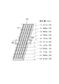
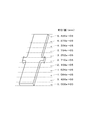
図3は、本実施形態に係る振動体210の剛性を示す図である。図4は、従来の振動体の剛性を示す図である。
上述の実施形態の効果を確認するために振動体210の剛性のシミュレーションを行った。振動体210の大きさは、縦が3.5mmで、横が1.00mmで、厚さが0.2mm(0.1mmを2枚)である。各接続部222,223の大きさは、横が0.25mmで、縦が0.3mmである。凹部12の大きさは、Φが0.1mmで、深さが0.05mmである。その配列は、縦が0.15mmで、横が0.2mmのピッチで片側23×5=115穴(両面に凹部12あり)である。
FIG. 3 is a diagram showing the rigidity of the vibrating
In order to confirm the effect of the above-described embodiment, the rigidity of the vibrating
シミュレーション結果を図3及び図4に示す。それぞれ同じ力で素子長辺方向に力を加えた時の各領域の変位(量)を求めており、変位が大きければ振動体210の剛性が低いということになる。図3のように振動体210に凹部12をパターン化して作った形状にすることで、図4の凹部のない形状に比べて変位(1N引張時の変位)が54nm(凹部なし)→70nm(凹部12あり)で約1.3倍になっている。つまり、圧電素子110へ同じ電力を加えた場合、変位が約1.3倍になる。変位が増えた分、出力が増加すると予測できる。同じ電力で出力が増加すれば、効率は向上する。
The simulation results are shown in FIGS. 3 and 4. The displacement (amount) of each region when a force is applied in the long side direction of the element with the same force is obtained, and if the displacement is large, the rigidity of the vibrating
振動体210の第1辺211には、凹部216が形成されている。凹部216には、被駆動部材と接触可能な接触子20が嵌め込まれて接合(通常は接着)される。接触子20は、被駆動部材と接触して、被駆動部材に力を与えるための部材である。接触子20は、セラミックス(例えばAl2O3)などの耐久性がある材料で形成することが好ましい。
A
図5は、圧電駆動装置10の等価回路を示す説明図である。図5に示す等価回路は、1つの圧電振動部100を動作するものを例として図示している。圧電素子110は、3つのグループに分けられる。第1グループは、2つの圧電素子110a,110dを有する。第2グループは、2つの圧電素子110b,110cを有する。第3グループは、1つの圧電素子110eのみを有する。第1グループの圧電素子110a,110dは、互いに並列に接続され、駆動回路300に接続されている。第2グループの圧電素子110b,110cは、互いに並列に接続され、駆動回路300に接続されている。第3グループの圧電素子110eは、単独で駆動回路300に接続されている。
FIG. 5 is an explanatory diagram showing an equivalent circuit of the
駆動回路300は、5つの圧電素子110a〜110eのうちの所定の圧電素子、例えば第1グループの圧電素子110a,110dの第1電極130と第2電極150との間に周期的に変化する交流電圧又は脈流電圧を印加することにより、圧電振動部100を超音波振動させて、接触子20に接触するローター(被駆動体、被駆動部材)を所定の回転方向に回転させることが可能である。ここで、「脈流電圧」とは、交流電圧にDCオフセットを付加した電圧を意味し、脈流電圧の電圧(電界)の向きは、一方の電極から他方の電極に向かう一方向である。電流の向きは、第1電極130から第2電極150に向かうよりも第2電極150から第1電極130に向かう方が好ましい。また、第2グループの圧電素子110b,110cの第1電極130と第2電極150との間に交流電圧又は脈流電圧を印加することにより、接触子20に接触するローターを逆方向に回転させることが可能である。
The
駆動回路300は、圧電素子110の共振周波数と同じ周波数の交流電圧又は脈流電圧を印加させてもよい。こうすることで、圧電素子110を滑らかに屈曲振動又は縦振動させることができる。本実施形態の圧電駆動装置10は、振動体210に凹部12を設けることにより、圧電素子110の共振周波数が下がる。また、縦共振と屈曲共振との差も変わるので、凹部12の個数や形状によって共振周波数の調整が可能である。さらに、凹部12の形状の分布や形状により、振動体210の剛性に異方性を持たせることができる。これにより、ローターと接する接触子20が描く軌跡の変位をコントロールでき、効率のよい駆動が実現できる。
The
図6は、圧電振動部100の動作の例を示す説明図である。圧電振動部100の接触子20は、被駆動部材としてのローター50の外周に接触している。図6に示す例では、第1グループの2つの圧電素子110a,110dに交流電圧又は脈流電圧を印加しており、圧電素子110a,110dは図6の矢印xの方向に伸縮する。これに応じて、圧電振動部100の振動体210が振動体210の平面内で屈曲して蛇行形状(S字形状)に変形し、接触子20の先端が矢印yの向きに往復運動するか、又は、楕円運動する。その結果、ローター50は、その中心51の周りに所定の方向z(図6では時計回り方向)に回転する。なお、駆動回路300が、第2グループの2つの圧電素子110b,110c(図1)に交流電圧又は脈流電圧を印加する場合には、ローター50は逆方向に回転する。なお、中央の圧電素子110eに、交流電圧又は脈流電圧を印加すれば、圧電駆動装置10が長手方向に伸縮するので、接触子20からローター50に与える力をより大きくすることが可能である。これによれば、圧電素子110a,110dの圧電体140に印加される電圧は一方向だけなので、圧電体140の耐久性を向上できる。なお、圧電駆動装置10(又は圧電振動部100)のこのような動作については、上記先行技術文献1(特開2004−320979号公報、又は、対応する米国特許第7224102号)に記載されており、その開示内容は参照により組み込まれる。
FIG. 6 is an explanatory diagram showing an example of the operation of the
図7は、本実施形態に係る圧電振動部100の製造工程で実行される膜形成プロセスを示すフローチャートを示す説明図である。図8は、本実施形態に係る圧電振動部100の製造工程を図示した説明図である。ステップS100では、基板200上に絶縁膜201を形成する。基板200として例えばSiウェハーを利用することができる。1枚のSiウェハー上には、圧電振動部100を複数個形成することが可能である。絶縁膜201としては、例えば、基板200の表面を熱酸化して形成されるSiO2膜を利用することができる。なお、図1では、絶縁膜201の図示が省略されている。その他、絶縁膜201としてアルミナ(Al2O3),アクリルやポリイミドなどの有機材料を用いることができる。なお、基板200が絶縁体である場合には、絶縁膜201を形成する工程は省略可能である。
FIG. 7 is an explanatory diagram showing a flowchart showing a film forming process executed in the manufacturing process of the
ステップS110では、第1電極130を形成し、パターニングする。第1電極130は、例えば、スパッタリングにより形成でき、パターニングは、エッチングにより行うことができる。
In step S110, the
ステップS120では、第1電極130の上に圧電体140を形成し、パターニングする。圧電体140を形成は、例えばゾル−ゲル法を用いて行うことが可能である。すなわち、圧電体材料のゾルゲル溶液を基板200(第1電極130)の上に滴下し、基板200を高速回転させることにより、第1電極130の上にゾルゲル溶液の薄膜を形成する。その後、200〜300℃の温度で仮焼きして第1電極130の上に圧電体材料の第1層を形成する。その後、ゾルゲル溶液の滴下、高速回転、仮焼き、のサイクルを複数回繰り返すことによって、第1電極130の上に所望の厚さまで圧電体膜を形成する。なお、1サイクルで形成される圧電体の一層の厚みは、ゾルゲル溶液の粘度や、基板200の回転速度にも依存するが、約50nm〜150nmの厚さとなる。所望の厚さまで圧電体膜を形成した後、600℃〜1000℃の温度で焼結することにより、圧電体140を形成する。焼結後の圧電体140の厚さを、50nm(0.05μm)以上20μm以下とすれば、小型の圧電駆動装置10を実現できる。なお、圧電体140の厚さを0.05μm以上とすれば、圧電体140の伸縮に応じて十分に大きな力を発生することができる。また、圧電体140の厚さを20μm以下とすれば、圧電体140に印加する電圧を600V以下としても十分に大きな力を発生することができる。その結果、圧電駆動装置10を駆動するための駆動回路300を安価な素子で構成できる。なお、圧電体の厚さを400nm以上としてもよく、この場合、圧電素子で発生する力を大きくできる。なお、仮焼きや焼結の温度、時間は、一例であり、圧電体材料により、適宜選択される。
In step S120, the
ゾル−ゲル法を用いて圧電体材料の薄膜を形成した後に焼結した場合には、原料粉末を混合して焼結する従来の焼結法と比較して、(a)薄膜を形成しやすい、(b)格子方向を揃えて結晶化し易い、(c)圧電体の耐圧を向上できる、というメリットがある。 When a thin film of a piezoelectric material is formed using the sol-gel method and then sintered, it is easier to form (a) a thin film as compared with the conventional sintering method in which raw material powders are mixed and sintered. , (B) It is easy to crystallize by aligning the lattice directions, and (c) It is possible to improve the withstand voltage of the piezoelectric material.
本実施形態では、ステップS120において、アルゴンイオンビームを用いたイオンミリングにより、圧電体140のパターニングを行っている。なお、イオンミリングを用いてパターニングを行う代わりに、他の任意のパターニング方法(例えば、塩素系のガスを用いたドライエッチング)によりパターニングを行っても良い。
In the present embodiment, in step S120, the
ステップS130では、圧電体140の上に第2電極150を形成し、パターニングする。第2電極150の形成及びパターニングは、第1電極130と同様に、スパッタリングとエッチングにより行うことができる。
In step S130, the
ステップS140では、第2電極150の上に絶縁膜240を形成する。ステップS150では、絶縁膜240の上に配線電極250を形成する。
In step S140, the insulating
図9は、配線電極250のパターンを示す説明図である。配線電極250は、4つの配線パターン251,252,253,254を有している。これらの配線パターン251〜254は、固定部221の上から接続部222,223の上を通って振動体210上に至るように形成されている。第1配線パターン251は、振動体210上で、圧電素子110a,110d(図1)の第2電極150と接続される。同様に、第2配線パターン252は、振動体210上で、圧電素子110b,110cの第2電極150と接続され、第3配線パターン253は、振動体210上で、圧電素子110eの第2電極150と接続され、第4配線パターン254は、振動体210上で、圧電素子110a,110b,110c,110d,110eの第1電極130と接続される。また、これらの配線パターン251〜254は、支持部220上(接続部222,223上を除く)で、駆動回路300からの配線と接続されている。なお、配線パターン251〜254は、固定部221上の第1電極130及び第2電極150とは接続されていない。
FIG. 9 is an explanatory diagram showing a pattern of the
ステップS160では、保護膜260を形成し、ステップS170では、エッチングにより、個々の基板200の形状を形成すると同時に、振動体210と、支持部220との間に隙間205を形成し、第1辺211に凹部216を形成する。凹部216には、接触子20が接着剤で接着される。また、振動体210の第2面218に凹部12を形成する。
In step S160, the
以上、本実施形態によれば、振動体210と支持部220(固定部221と接続部222,223)とが一体成形されており、振動体210の少なくとも一方の面に第1電極130と圧電体140と第2電極150とで一体に形成された圧電素子110を備える。したがって、振動体210と圧電素子110との間に接着剤膜がなく、駆動力の伝達ロスが発生し難い。
As described above, according to the present embodiment, the vibrating
図10は、圧電駆動装置の構成例を示す説明図である。図10(A)及び(B)は4つの圧電振動部100a,100b,100c,100dを備えている図であり、図10(C)は2つの圧電振動部100e,100fを備えている図である。
図10(A)に示す圧電駆動装置10aは、4つの圧電振動部100a,100b,100c,100dを備えている。各圧電振動部100a〜100dは、上述した圧電振動部100と同様に、振動体210と支持部220とを備えている。第2圧電振動部100bの支持部や固定部を「第2支持部」及び「第2固定部」と呼ぶ。以下、第3圧電振動部100c、第4圧電振動部100dについても同様である。この例では、第2圧電振動部100bは、第1圧電振動部100aの振動体210と、第1圧電振動部100aに隣接する第2圧電振動部100bの圧電素子110(第2圧電素子)とが接着剤膜270により接着されている。これによれば、振動体210表面の凹部12形状が接着剤膜270の逃げの役割を果たし、接着剤膜270のはみ出しを防ぐことができる。
FIG. 10 is an explanatory diagram showing a configuration example of the piezoelectric drive device. 10 (A) and 10 (B) are views including four
The
図10(B)に示す圧電駆動装置10bも、同様に4つの圧電振動部100a,100b,100c,100dを備えている。ただし、図10(B)では、第1圧電振動部100aの振動体210と、第1圧電振動部100aに隣接する第2圧電振動部100bの振動体210(「第2振動体210」とも呼ぶ。)と、が接着剤膜270により接着され、第2圧電振動部100bの圧電素子110と、第2圧電振動部100bに隣接する第3圧電振動部100cの圧電素子110と、が接着剤膜270により接着されている。これによれば、振動体210表面の凹部12形状が接着剤膜270の逃げの役割を果たし、接着剤膜270のはみ出しを防ぐことができる。
The
なお、第1圧電振動部100aの振動体210と、第1圧電振動部100aに隣接する第2圧電振動部100bの振動体210(「第2振動体210」とも呼ぶ。)とは、接着剤膜270の有無にかかわらず、凹部12同士をずらして(図面上左右)嵌合してもよい。
The vibrating
図10(C)に示す圧電駆動装置10cは、2つの圧電振動部100e,100fを備えており、これらの圧電振動部100e,100fは、いずれも振動体210の両面に圧電素子110を備える構成である。第1圧電振動部100eの圧電素子110と、第1圧電振動部100eに隣接する第2圧電振動部100fの圧電素子110とが接着剤膜270により接着されている。
The
このように、圧電駆動装置10は、2以上の圧電振動部100を振動体210の法線方向に積層した構成を備えていても良い。これにより、駆動力を大きくできる。なお、本実施形態では、圧電駆動装置10は、2以上の圧電振動部100を振動体210の法線方向に積層した構成を備えているが、2以上の圧電振動部100を振動体210の平面に沿って配置しても良い。これによれば、2以上の圧電振動部100を振動体210の法線方向に積層した構成と比較して、圧電駆動装置10を薄型化することができる。
As described above, the
図11は、他の実施形態としての圧電振動部の平面図であり、第1実施形態の図1(A)に対応する図である。図11(A)は3つの圧電素子110a,110e,110dが形成されている図であり、図11(B)は4つの圧電素子110a,110b,110c,110dが形成されている図であり、図11(C)は1つの第2電極150eが形成されている図である。図11(A)、(B)、及び(C)では、図示の便宜上、振動体210のみを図示し、支持部220や接続部222,223は、図示が省略されている。図11(A)の圧電振動部100gでは、一対の圧電素子110b,110cが省略されている。この圧電振動部100gも、図6に示すような1つの方向zにローター50を回転させることが可能である。なお、図11(A)の3つの圧電素子110a,110e,110dには同じ電圧が印加されるので、これらの3つの圧電素子110a,110e,110dの第2電極(150a,150e,150d)を、連続する1つの電極膜として形成してもよい。
FIG. 11 is a plan view of the piezoelectric vibration unit as another embodiment, and is a diagram corresponding to FIG. 1 (A) of the first embodiment. FIG. 11A is a diagram in which three
図11(B)は、本発明のさらに他の実施形態としての圧電振動部100hの平面図である。この圧電振動部100hでは、図1(A)の中央の圧電素子110eが省略されており、他の4つの圧電素子110a,110b,110c,110dが図1(A)よりも大きな面積に形成されている。この圧電振動部100cも、第1実施形態とほぼ同様な効果を達成することができる。
FIG. 11B is a plan view of the piezoelectric vibrating
図11(C)は、本発明のさらに他の実施形態としての圧電振動部100jの平面図である。この圧電振動部100jでは、図1(A)の4つの第2電極150a,150b,150c,150dが省略されており、1つの第2電極150eが大きな面積で形成されている。この圧電振動部100dは、長手方向に伸縮するだけであるが、接触子20から被駆動体(図示省略)に対して大きな力を与えることが可能である。
FIG. 11C is a plan view of the piezoelectric vibrating
図1及び図11(A)、(B)、及び(C)から理解できるように、圧電振動部100の第2電極150としては、少なくとも1つの電極膜を設けることができる。ただし、図1及び図11(A)及び(B)に示す実施形態のように、長方形の振動体210の対角の位置に圧電素子110(第2電極150)を設けるようにすれば、振動体210を、その平面内で屈曲する蛇行形状に変形させることが可能である点で好ましい。
As can be understood from FIGS. 1 and 11 (A), (B), and (C), at least one electrode film can be provided as the
図12は、圧電振動部100の別の構成を示す説明図である。圧電振動部100kは、図1に示す圧電振動部100と比較すると、以下の点が異なっている。図1に示す圧電振動部100では、基板200の上に圧電素子110が形成され、その上に絶縁膜240と配線電極250と保護膜260とが形成されている。図12に示す圧電振動部100kでは、基板200の上に絶縁膜240と配線電極250と絶縁膜265とが形成され、絶縁膜265の上に圧電素子110が配置されている。すなわち、圧電体140よりも基板200側に配線電極250が形成される。このような構成であっても良い。この構成の場合、配線電極250の下層に圧電体140がなく、圧電体140の厚さの影響を受けないので、配線電極250が断線しにくいという効果がある。
FIG. 12 is an explanatory diagram showing another configuration of the
(圧電駆動装置を用いた装置の実施形態)
上述した圧電駆動装置10は、共振を利用することで被駆動部材に対して大きな力を与えることができるものであり、各種の装置に適用可能である。圧電駆動装置10は、例えば、ロボット(電子部品搬送装置(ICハンドラー)も含む)、投薬用ポンプ、時計のカレンダー送り装置、印刷装置(例えば紙送り機構。ただし、ヘッドに利用される圧電駆動装置では、振動板を共振させないので、ヘッドには適用不可である。)等の各種の機器における駆動装置として用いることができる。以下、代表的な実施の形態について説明する。
(Embodiment of a device using a piezoelectric drive device)
The above-mentioned
図13は、上述の圧電駆動装置10を利用したロボット2050の一例を示す説明図である。ロボット2050は、複数本のリンク部2012(「リンク部材」とも呼ぶ)と、それらリンク部2012の間を回動又は屈曲可能な状態で接続する複数の関節部2020とを備えたアーム2010(「腕部」とも呼ぶ)を有している。それぞれの関節部2020には、上述した圧電駆動装置10が内蔵されており、圧電駆動装置10を用いて関節部2020を任意の角度だけ回動又は屈曲させることが可能である。アーム2010の先端には、ロボットハンド2000が接続されている。ロボットハンド2000は、一対の把持部2003を備えている。ロボットハンド2000にも圧電駆動装置10が内蔵されており、圧電駆動装置10を用いて把持部2003を開閉してものを把持することが可能である。また、ロボットハンド2000とアーム2010との間にも圧電駆動装置10が設けられており、圧電駆動装置10を用いてロボットハンド2000をアーム2010に対して回転させることも可能である。
FIG. 13 is an explanatory diagram showing an example of the
図14は、図13に示したロボット2050の手首部分の説明図である。手首の関節部2020は、手首回動部2022を挟持しており、手首回動部2022に手首のリンク部2012が、手首回動部2022の中心軸O周りに回動可能に取り付けられている。手首回動部2022は、圧電駆動装置10を備えており、圧電駆動装置10は、手首のリンク部2012及びロボットハンド2000を中心軸O周りに回動させる。ロボットハンド2000には、複数の把持部2003が立設されている。把持部2003の基端部はロボットハンド2000内で移動可能となっており、この把持部2003の根元の部分に圧電駆動装置10が搭載されている。このため、圧電駆動装置10を動作させることで、把持部2003を移動させて対象物を把持することができる。
FIG. 14 is an explanatory view of the wrist portion of the
なお、ロボットとしては、単腕のロボットに限らず、腕の数が2以上の多腕ロボットにも圧電駆動装置10を適用可能である。ここで、手首の関節部2020やロボットハンド2000の内部には、圧電駆動装置10の他に、力覚センサーやジャイロセンサー等の各種装置に電力を供給する電力線や、信号を伝達する信号線等が含まれ、非常に多くの配線が必要になる。したがって、関節部2020やロボットハンド2000の内部に配線を配置することは非常に困難だった。しかしながら、上述した実施形態の圧電駆動装置10は、通常の電動モーターや、従来の圧電駆動装置よりも駆動電流を小さくできるので、関節部2020(特に、アーム2010の先端の関節部)やロボットハンド2000のような小さな空間でも配線を配置することが可能になる。
The robot is not limited to a single-arm robot, but the
図15は、上述の圧電駆動装置10を利用した送液ポンプ2200の一例を示す説明図である。送液ポンプ2200は、ケース2230内に、リザーバー2211と、チューブ2212と、圧電駆動装置10と、ローター2222と、減速伝達機構2223と、カム2202と、複数のフィンガー2213,2214,2215,2216,2217,2218,2219と、が設けられている。リザーバー2211は、輸送対象である液体を収容するための収容部である。チューブ2212は、リザーバー2211から送り出される液体を輸送するための管である。圧電駆動装置10の接触子20は、ローター2222の側面に押し付けた状態で設けられており、圧電駆動装置10がローター2222を回転駆動する。ローター2222の回転力は減速伝達機構2223を介してカム2202に伝達される。フィンガー2213〜2219はチューブ2212を閉塞させるための部材である。カム2202が回転すると、カム2202の突起部2202Aによってフィンガー2213〜2219が順番に放射方向外側に押される。フィンガー2213〜2219は、輸送方向上流側(リザーバー2211側)から順にチューブ2212を閉塞する。これにより、チューブ2212内の液体が順に下流側に輸送される。こうすれば、極く僅かな量を精度良く送液可能で、しかも小型な送液ポンプ2200を実現することができる。なお、各部材の配置は図示されたものには限られない。また、フィンガーなどの部材を備えず、ローター2222に設けられたボールなどがチューブ2212を閉塞する構成であってもよい。上記のような送液ポンプ2200は、インシュリンなどの薬液を人体に投与する投薬装置などに活用できる。ここで、上述した実施形態の圧電駆動装置10を用いることにより、従来の圧電駆動装置よりも駆動電流が小さくなるので、投薬装置の消費電力を抑制することができる。したがって、投薬装置を電池駆動する場合は、特に有効である。
FIG. 15 is an explanatory diagram showing an example of a
以上、いくつかの実施例に基づいて本発明の実施の形態について説明してきたが、上記した発明の実施の形態は、本発明の理解を容易にするためのものであり、本発明を限定するものではない。本発明は、その趣旨並びに特許請求の範囲を逸脱することなく、変更、改良され得るとともに、本発明にはその等価物が含まれることはもちろんである。 Although the embodiments of the present invention have been described above based on some examples, the above-described embodiments of the invention are for facilitating the understanding of the present invention and limit the present invention. It's not a thing. The present invention can be modified and improved without departing from the spirit and claims, and it goes without saying that the present invention includes an equivalent thereof.
10,10a,10b,10c…圧電駆動装置 12…凹部 20…接触子 50…ローター 51…中心 100,100a,100b,100c,100d,100e,100f,100g,100h,100j,100k…圧電振動部 110,110a,110b,110c,110d,110e…圧電素子 130…第1電極(第1電極膜) 140…圧電体(圧電体膜) 150,150a,150b,150c,150d,150e…第2電極(第2電極膜) 200…基板 201…絶縁膜 205…隙間 210…振動体 211…第1辺 212…第2辺 213…第3辺 214…第4辺 216…凹部 217…第1面 218…第2面 220…支持部 221…固定部 222…第1接続部 223…第2接続部 240…絶縁膜 250…配線電極 251,252,253,254…配線パターン 260…保護膜 265…絶縁膜 270…接着剤膜 300…駆動回路 2000…ロボットハンド 2003…把持部 2010…アーム 2012…リンク部 2020…関節部 2022…手首回動部 2050…ロボット 2200…送液ポンプ 2202…カム 2202A…突起部 2211…リザーバー 2212…チューブ 2213〜2219…フィンガー 2222…ローター 2223…減速伝達機構 2230…ケース。
10, 10a, 10b, 10c ...
Claims (9)
前記第1面に設けられた圧電素子と、
前記振動体と前記圧電素子とを含む第1圧電振動部及び第2圧電振動部と、を含み、
前記凹部は、円柱状の形状であり、第2面から第1面へ貫通せず、
前記凹部と前記圧電素子とは、前記第2面の法線方向から見て、重なる部分を有し、
前記第1圧電振動部の前記第2面と前記第2圧電振動部の前記第2面とが接着されていることを特徴とする圧電駆動装置。 A vibrating body having a first surface and a second surface on the back surface side of the first surface and having a recess formed therein.
The piezoelectric element provided on the first surface and
A first piezoelectric vibrating portion and a second piezoelectric vibrating portion including the vibrating body and the piezoelectric element are included.
The recess has a columnar shape and does not penetrate from the second surface to the first surface.
Wherein said recess and the piezoelectric element, when viewed from the normal direction of the second surface, have a portion overlapping,
A piezoelectric drive device characterized in that the second surface of the first piezoelectric vibrating portion and the second surface of the second piezoelectric vibrating portion are adhered to each other .
前記第2面の法線方向から見て、
前記振動体は、第1線に対して対称な形状であり、
前記凹部は、前記第1線に対して対称に配置されていることを特徴とする圧電駆動装置。 In the piezoelectric drive device according to claim 1,
Seen from the normal direction of the second surface
The vibrating body has a shape symmetrical with respect to the first line.
A piezoelectric drive device characterized in that the recesses are arranged symmetrically with respect to the first line.
前記第2面の法線方向から見て、
前記振動体は、第1線に対して対称な形状であり、
前記凹部は、前記第1線に対して非対称に配置されていることを特徴とする圧電駆動装置。 In the piezoelectric drive device according to claim 1 or 2.
Seen from the normal direction of the second surface
The vibrating body has a shape symmetrical with respect to the first line.
A piezoelectric drive device characterized in that the recesses are arranged asymmetrically with respect to the first line.
前記第1面は、平坦であることを特徴とする圧電駆動装置。 In the piezoelectric drive device according to any one of claims 1 to 3.
The first surface is a piezoelectric drive device characterized by being flat.
前記圧電素子は、第1電極、第2電極、及び前記第1電極と前記第2電極との間に位置する圧電体を有し、
前記圧電体の厚さは、50nm以上20μm以下であることを特徴とする圧電駆動装置。 In the piezoelectric drive device according to any one of claims 1 to 4.
The piezoelectric element has a first electrode, a second electrode, and a piezoelectric body located between the first electrode and the second electrode.
A piezoelectric driving device characterized in that the thickness of the piezoelectric body is 50 nm or more and 20 μm or less.
前記振動体は、シリコンを含むことを特徴とする圧電駆動装置。 In the piezoelectric drive device according to any one of claims 1 to 5.
The vibrating body is a piezoelectric driving device characterized by containing silicon.
前記振動体に接続されている支持部を含むことを特徴とする圧電駆動装置。 In the piezoelectric drive device according to any one of claims 1 to 6.
A piezoelectric drive device including a support portion connected to the vibrating body .
前記複数のリンク部を接続する関節部と、
前記リンク部を前記関節部で回動させる請求項1〜7のいずれか一項に記載の圧電駆動装置と、
を有することを特徴とするロボット。 With multiple links
The joints that connect the plurality of links and
The piezoelectric drive device according to any one of claims 1 to 7 , wherein the link portion is rotated by the joint portion.
A robot characterized by having.
前記圧電駆動装置は、第1電極、第2電極、及び前記第1電極と前記第2電極との間に位置する圧電体を有し、
前記第1電極と前記第2電極との間に、周期的に変化する電圧を印加することを特徴とする圧電駆動装置の駆動方法。 The method for driving a piezoelectric driving device according to any one of claims 1 to 7 .
The piezoelectric drive device has a first electrode, a second electrode, and a piezoelectric body located between the first electrode and the second electrode.
A method for driving a piezoelectric drive device, characterized in that a voltage that changes periodically is applied between the first electrode and the second electrode.
Priority Applications (3)
| Application Number | Priority Date | Filing Date | Title |
|---|---|---|---|
| JP2015150424A JP6766328B2 (en) | 2015-07-30 | 2015-07-30 | Piezoelectric drive, robots, and methods of driving piezoelectric drives |
| PCT/JP2016/003213 WO2017017907A1 (en) | 2015-07-30 | 2016-07-06 | Piezoelectric drive device, robot and method for driving piezoelectric drive device |
| US15/748,382 US11107969B2 (en) | 2015-07-30 | 2016-07-06 | Piezoelectric drive device, robot, and method for driving piezoelectric drive device |
Applications Claiming Priority (1)
| Application Number | Priority Date | Filing Date | Title |
|---|---|---|---|
| JP2015150424A JP6766328B2 (en) | 2015-07-30 | 2015-07-30 | Piezoelectric drive, robots, and methods of driving piezoelectric drives |
Publications (3)
| Publication Number | Publication Date |
|---|---|
| JP2017034784A JP2017034784A (en) | 2017-02-09 |
| JP2017034784A5 JP2017034784A5 (en) | 2018-09-06 |
| JP6766328B2 true JP6766328B2 (en) | 2020-10-14 |
Family
ID=57884407
Family Applications (1)
| Application Number | Title | Priority Date | Filing Date |
|---|---|---|---|
| JP2015150424A Active JP6766328B2 (en) | 2015-07-30 | 2015-07-30 | Piezoelectric drive, robots, and methods of driving piezoelectric drives |
Country Status (3)
| Country | Link |
|---|---|
| US (1) | US11107969B2 (en) |
| JP (1) | JP6766328B2 (en) |
| WO (1) | WO2017017907A1 (en) |
Families Citing this family (3)
| Publication number | Priority date | Publication date | Assignee | Title |
|---|---|---|---|---|
| US10601397B2 (en) * | 2017-03-24 | 2020-03-24 | Zhuhai Crystal Resonance Technologies Co., Ltd. | RF resonator electrode and membrane combinations and method of fabrication |
| DE102017009542B3 (en) * | 2017-10-13 | 2019-01-03 | Marco Systemanalyse Und Entwicklung Gmbh | positioning |
| KR102486154B1 (en) | 2018-11-02 | 2023-01-10 | 엘지디스플레이 주식회사 | Ultrasonic sensor, ultrasonic sensing device and display device |
Family Cites Families (13)
| Publication number | Priority date | Publication date | Assignee | Title |
|---|---|---|---|---|
| JPH07108102B2 (en) * | 1990-05-01 | 1995-11-15 | 日本碍子株式会社 | Method for manufacturing piezoelectric / electrostrictive film type actuator |
| US5389849A (en) * | 1993-01-20 | 1995-02-14 | Olympus Optical Co., Ltd. | Tactility providing apparatus and manipulating device using the same |
| JPH09182468A (en) | 1995-12-28 | 1997-07-11 | Nikon Corp | Oscillatory actuator |
| JP3124514B2 (en) * | 1997-08-01 | 2001-01-15 | セイコーインスツルメンツ株式会社 | Ultrasonic motors, electronic devices, and analog watches |
| JP2003008094A (en) | 2001-06-19 | 2003-01-10 | Seiko Instruments Inc | Piezoelectric device and its manufacturing method |
| JP2003134861A (en) | 2001-10-26 | 2003-05-09 | Taiheiyo Cement Corp | Piezoelectric actuator |
| JP4454930B2 (en) | 2002-11-29 | 2010-04-21 | セイコーインスツル株式会社 | Ultrasonic motor and electronic device with ultrasonic motor |
| JP2004320979A (en) | 2003-04-03 | 2004-11-11 | Seiko Epson Corp | Driving device and electric equipment |
| JP6020022B2 (en) | 2012-10-17 | 2016-11-02 | セイコーエプソン株式会社 | Piezoelectric actuator, robot hand, robot, electronic component transport device, electronic component inspection device, liquid feed pump, printing device, electronic watch, projection device, transport device |
| JP6296227B2 (en) * | 2013-11-22 | 2018-03-20 | セイコーエプソン株式会社 | Liquid ejecting head, liquid ejecting apparatus, and piezoelectric element |
| CN104887364B (en) * | 2014-03-03 | 2018-11-02 | 精工爱普生株式会社 | Articulations digitorum manus driving device |
| CN105267007B (en) * | 2014-05-29 | 2019-03-08 | 精工爱普生株式会社 | Driving device and its driving method |
| JP6485118B2 (en) * | 2015-03-04 | 2019-03-20 | セイコーエプソン株式会社 | Piezoelectric drive device and robot |
-
2015
- 2015-07-30 JP JP2015150424A patent/JP6766328B2/en active Active
-
2016
- 2016-07-06 US US15/748,382 patent/US11107969B2/en active Active
- 2016-07-06 WO PCT/JP2016/003213 patent/WO2017017907A1/en active Application Filing
Also Published As
| Publication number | Publication date |
|---|---|
| WO2017017907A1 (en) | 2017-02-02 |
| JP2017034784A (en) | 2017-02-09 |
| US20180226561A1 (en) | 2018-08-09 |
| US11107969B2 (en) | 2021-08-31 |
Similar Documents
| Publication | Publication Date | Title |
|---|---|---|
| EP3121861B1 (en) | Piezoelectric drive device, robot, and method for driving piezoelectric drive device | |
| JP6405785B2 (en) | Piezoelectric drive device, robot, and drive method thereof | |
| JP6511900B2 (en) | Piezoelectric drive device and drive method therefor, robot and drive method therefor | |
| JP6398454B2 (en) | Piezoelectric drive device, robot, and drive method thereof | |
| JP6543951B2 (en) | Piezoelectric drive device, robot, and method of driving them | |
| EP3051688B1 (en) | Piezoelectric drive device, robot, and drive method of robot | |
| JP6641944B2 (en) | Piezoelectric drive device for motor and method of manufacturing the same, motor, robot, and pump | |
| US10147866B2 (en) | Piezoelectric driving device and driving method therefor, and robot and driving method therefor | |
| JP6503940B2 (en) | Piezoelectric drive device, robot and drive method of piezoelectric drive device | |
| JP6766328B2 (en) | Piezoelectric drive, robots, and methods of driving piezoelectric drives | |
| US10097111B2 (en) | Piezoelectric drive device and robot | |
| JP6503764B2 (en) | Piezoelectric element drive circuit and robot | |
| JP6442913B2 (en) | Piezoelectric drive device, robot, and drive method thereof | |
| JP6601174B2 (en) | Piezoelectric actuators, stacked actuators, piezoelectric motors, robots, hands and liquid pumps | |
| JP2016040984A (en) | Piezoelectric drive device and drive method of the same, robot and drive method of the robot | |
| JP6432204B2 (en) | Piezoelectric drive device, robot, and drive method thereof | |
| JP6662007B2 (en) | Piezo drives, motors, robots, and pumps | |
| JP6702482B2 (en) | Piezoelectric driving device and driving method thereof, robot and driving method thereof | |
| JP2017135935A (en) | Piezoelectric actuator, piezoelectric motor, robot, hand and feed pump | |
| JP6413461B2 (en) | Piezoelectric driving device and driving method thereof, robot and driving method thereof | |
| JP6432369B2 (en) | Piezoelectric driving device, robot, and robot driving method |
Legal Events
| Date | Code | Title | Description |
|---|---|---|---|
| A521 | Request for written amendment filed |
Free format text: JAPANESE INTERMEDIATE CODE: A523 Effective date: 20180720 |
|
| A621 | Written request for application examination |
Free format text: JAPANESE INTERMEDIATE CODE: A621 Effective date: 20180720 |
|
| RD05 | Notification of revocation of power of attorney |
Free format text: JAPANESE INTERMEDIATE CODE: A7425 Effective date: 20180906 |
|
| RD03 | Notification of appointment of power of attorney |
Free format text: JAPANESE INTERMEDIATE CODE: A7423 Effective date: 20181116 |
|
| A131 | Notification of reasons for refusal |
Free format text: JAPANESE INTERMEDIATE CODE: A131 Effective date: 20190820 |
|
| A521 | Request for written amendment filed |
Free format text: JAPANESE INTERMEDIATE CODE: A523 Effective date: 20191016 |
|
| A131 | Notification of reasons for refusal |
Free format text: JAPANESE INTERMEDIATE CODE: A131 Effective date: 20200212 |
|
| A521 | Request for written amendment filed |
Free format text: JAPANESE INTERMEDIATE CODE: A523 Effective date: 20200326 |
|
| RD07 | Notification of extinguishment of power of attorney |
Free format text: JAPANESE INTERMEDIATE CODE: A7427 Effective date: 20200803 |
|
| TRDD | Decision of grant or rejection written | ||
| A01 | Written decision to grant a patent or to grant a registration (utility model) |
Free format text: JAPANESE INTERMEDIATE CODE: A01 Effective date: 20200818 |
|
| A61 | First payment of annual fees (during grant procedure) |
Free format text: JAPANESE INTERMEDIATE CODE: A61 Effective date: 20200831 |
|
| R150 | Certificate of patent or registration of utility model |
Ref document number: 6766328 Country of ref document: JP Free format text: JAPANESE INTERMEDIATE CODE: R150 |