EP2979357B1 - Radio-frequency device calibration - Google Patents
Radio-frequency device calibration Download PDFInfo
- Publication number
- EP2979357B1 EP2979357B1 EP14716147.5A EP14716147A EP2979357B1 EP 2979357 B1 EP2979357 B1 EP 2979357B1 EP 14716147 A EP14716147 A EP 14716147A EP 2979357 B1 EP2979357 B1 EP 2979357B1
- Authority
- EP
- European Patent Office
- Prior art keywords
- power amplifier
- voltage
- output voltage
- bias voltage
- relationship
- Prior art date
- Legal status (The legal status is an assumption and is not a legal conclusion. Google has not performed a legal analysis and makes no representation as to the accuracy of the status listed.)
- Active
Links
- 230000006835 compression Effects 0.000 claims description 46
- 238000007906 compression Methods 0.000 claims description 46
- 238000000034 method Methods 0.000 claims description 35
- 238000005516 engineering process Methods 0.000 claims description 33
- 238000013461 design Methods 0.000 description 7
- 238000004891 communication Methods 0.000 description 6
- 230000006870 function Effects 0.000 description 5
- 238000007796 conventional method Methods 0.000 description 3
- 230000003287 optical effect Effects 0.000 description 3
- 230000008901 benefit Effects 0.000 description 2
- 230000008859 change Effects 0.000 description 2
- 238000012512 characterization method Methods 0.000 description 2
- 238000006243 chemical reaction Methods 0.000 description 2
- 230000003750 conditioning effect Effects 0.000 description 2
- 238000010586 diagram Methods 0.000 description 2
- 239000000835 fiber Substances 0.000 description 2
- 239000002245 particle Substances 0.000 description 2
- 238000012546 transfer Methods 0.000 description 2
- 238000013459 approach Methods 0.000 description 1
- 238000004590 computer program Methods 0.000 description 1
- 230000003247 decreasing effect Effects 0.000 description 1
- 238000004519 manufacturing process Methods 0.000 description 1
- 238000012986 modification Methods 0.000 description 1
- 230000004048 modification Effects 0.000 description 1
- 230000008569 process Effects 0.000 description 1
- 238000012545 processing Methods 0.000 description 1
- 230000004044 response Effects 0.000 description 1
- 238000001228 spectrum Methods 0.000 description 1
- 230000003068 static effect Effects 0.000 description 1
Images


Classifications
-
- H—ELECTRICITY
- H03—ELECTRONIC CIRCUITRY
- H03F—AMPLIFIERS
- H03F1/00—Details of amplifiers with only discharge tubes, only semiconductor devices or only unspecified devices as amplifying elements
- H03F1/02—Modifications of amplifiers to raise the efficiency, e.g. gliding Class A stages, use of an auxiliary oscillation
- H03F1/0205—Modifications of amplifiers to raise the efficiency, e.g. gliding Class A stages, use of an auxiliary oscillation in transistor amplifiers
- H03F1/0211—Modifications of amplifiers to raise the efficiency, e.g. gliding Class A stages, use of an auxiliary oscillation in transistor amplifiers with control of the supply voltage or current
-
- H—ELECTRICITY
- H03—ELECTRONIC CIRCUITRY
- H03F—AMPLIFIERS
- H03F1/00—Details of amplifiers with only discharge tubes, only semiconductor devices or only unspecified devices as amplifying elements
- H03F1/32—Modifications of amplifiers to reduce non-linear distortion
- H03F1/3241—Modifications of amplifiers to reduce non-linear distortion using predistortion circuits
- H03F1/3247—Modifications of amplifiers to reduce non-linear distortion using predistortion circuits using feedback acting on predistortion circuits
-
- H—ELECTRICITY
- H03—ELECTRONIC CIRCUITRY
- H03F—AMPLIFIERS
- H03F3/00—Amplifiers with only discharge tubes or only semiconductor devices as amplifying elements
- H03F3/189—High-frequency amplifiers, e.g. radio frequency amplifiers
-
- H—ELECTRICITY
- H03—ELECTRONIC CIRCUITRY
- H03F—AMPLIFIERS
- H03F3/00—Amplifiers with only discharge tubes or only semiconductor devices as amplifying elements
- H03F3/20—Power amplifiers, e.g. Class B amplifiers, Class C amplifiers
Definitions
- the present invention relates generally to calibration of a radio-frequency (RF) transmitter. More specifically, the present invention relates to embodiments for calibrating a power amplifier device with digital pre-distortion.
- RF radio-frequency
- Electronic amplifiers are used for increasing a power and/or an amplitude of various electronic signals. Most electronic amplifiers operate by using power from a power supply, and controlling an output signal to match the shape of an input signal, while providing a higher amplitude signal.
- a power amplifier which is a versatile device used in various applications to meet design requirements for signal conditioning, special transfer functions, analog instrumentation, and analog computation, among others.
- Power amplifiers are often used in wireless applications, and may employ RF amplifier designs for use in the RF range of the electromagnetic spectrum.
- An RF power amplifier is a type of electronic amplifier used to convert a low-power RF signal into a signal of significant power, typically for driving an antenna of a transmitter.
- RF power amplifiers are oftentimes used to increase the range of a wireless communication system by increasing the output power of a transmitter.
- Power amplifiers typically, do not behave in a linear manner. More particularly, power amplifier distortion may compress or may expand an output signal swing of a power amplifier. Signal detectors receiving and decoding the amplified signals typically do not operate in such a non-linear fashion. Therefore, it is usually necessary to linearize an output of a power amplifier.
- One approach to such linearization is digital pre-distortion (DPD). DPD may be calibrated and used with power amplifiers to invert power amplifier distortion characteristics by expanding compression regions and compressing expansion regions of power amplifier characteristics.
- DPD digital pre-distortion
- APT average power tracking
- ET envelope tracking
- DAC digital-to-analog converter
- each power amplifier control technology may have a target compression value, which may also be referred to as a target compression point.
- APT has a target compression value of 1.5 dB
- EPT has a target compression value of 2 dB
- ET has a target compression value of 3 dB.
- one or more other control technologies may have a target compression value of 2 dB.
- a conventional method of characterizing a power amplifier digital pre-distortion device may include measuring a few parts (i.e., a few amplifiers of a batch), and using an average of the parts, or a worst case scenario.
- this method suffers due to a power amplifier's part-to-part amplitude modulation-to-amplitude modulation (AM-AM) variation and/or amplitude modulation-to-phase modulation (AM-PM) variation.
- AM-AM part-to-part amplitude modulation-to-amplitude modulation
- AM-PM amplitude modulation-to-phase modulation
- Exemplary embodiments of the present invention include embodiments for determining a relationship among three variables (i.e., input voltage Vin, output voltage Vout, and bias voltage Vcc) of a power amplifier based on a desired compression point for the power amplifier.
- the relationship data may then be used for determining a power amplifier's AM-AM per part.
- a gain index which controls a power amplifier input voltage level, and voltage level of a bias signal (“bias voltage”) conveyed to the power amplifier (i.e., power amplifier bias voltage) for each desired power level of a signal output by the power amplifier (i.e., a power amplifier output voltage) may be calculated.
- the relationship data may be shared among a plurality of control technologies.
- a device may include a power amplifier configured to receive an input voltage and a bias voltage and convey an output voltage.
- the device may also include a processor coupled to the power amplifier and configured to sense a plurality of in-phase and quadrature (IQ) samples conveyed by the power amplifier at a plurality of input voltages and bias voltages conveyed to the power amplifier.
- the processor may also be configured to generate a plurality of AM-AM curves from the plurality of sensed IQ samples.
- the processor may be configured to determine a relationship among the input voltage, the bias voltage, and the output voltage based on target compression point on each curve for each power amplifier control technology.
- the processor may further be configured to determine, based on the relationship, two of the input voltage, the bias voltage, and the output voltage to reach the target compression point based on a known value for one of the input voltage, bias voltage, and the output voltage.
- the present invention includes methods for calibrating a power amplifier digital pre-distortion device.
- Various embodiments of such a method may include calibrating an RF device by calculating input voltage values and bias voltage values of a power amplifier for each desired output voltage value of the power amplifier to generate a desired compression point.
- the method may also include applying DPD values to the input voltage of the power amplifier, and measuring a value of the output voltage after applying the DPD values.
- a method may include sensing a plurality of IQ samples conveyed by the power amplifier at a plurality of input voltages and bias voltages conveyed to the power amplifier.
- the method may include generating a plurality of AM-AM curves from the plurality of sensed IQ samples.
- the method may further include determining a relationship among the input voltage, the bias voltage, and the output voltage based on target compression point on each curve for each power amplifier control technology.
- the method may include determining, based on the relationship, two of the input voltage, the bias voltage, and the output voltage to reach the target compression point based on a known value for one of the input voltage, bias voltage, and the output voltage.
- FIG. 1 illustrates a device 100 including a DPD unit 102, gain unit 104, a power amplifier 106, and a processor 108. It is noted that device 100 is an example of a power amplifier digital pre-distortion device, which may be used for carrying out one or more of the various methods described herein.
- FIG. 2 depicts a device 200, which is a more detailed example of a power amplifier digital pre-distortion device that may be used for carrying out one or more of the various methods described herein.
- Device 200 includes a modulator 202, a pre-DPD gain unit 204, and a linearized system 205.
- Linearized system 205 includes a DPD unit 206, a post-DPD gain unit 208, a digital-to-analog converter (DAC) 210, an RF gain index 212, a power amplifier 214, and a duplexer 216.
- Power amplifier 214 may be configured to receive an input voltage and a bias voltage, and output an output voltage.
- post-DPD gain unit 208, RF gain index 212, or both may be varied to modify a power level of a signal received by power amplifier 214.
- Device 200 may further include a processor 108 for receiving an output of duplexer 216 controlling an operation of one or more of the components of device 200.
- processor 108 may be configured for capturing IQ samples at a plurality of input and bias voltages (e.g., input voltages of the power amplifier 214 and voltages for biasing the power amplifier 214).
- processor 108 may include a DPD capture unit (not shown in FIG. 2 ) configured for capturing IQ samples. It is noted that processor 108 may include one or more memory devices for storing data related to calibration of a device 100/200, as described herein.
- a plurality of IQ samples may be captured at a various input and bias voltages.
- a plurality of IQ samples may be captured at four predetermined voltage combinations (i.e., power amplifier input voltage and bias voltage combinations).
- each IQ capture may result in an AM-AM curve on a plot. More specifically, if a processor captures four IQ samples, the processor may generate a plot including four AM-AM curves, wherein each curve is associated with a specific bias voltage.
- a desired compression point on each AM-AM curve may be identified, and the plot may be scaled by extending a line linearly through each compression point to identify additional AM-AM curves. More specifically, as long as the plot includes at least two AM-AM curves, wherein each curve includes a desired compression, the plot may be scaled to include more than the two AM-AM curves.
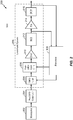
- the power amplifier digital pre-distortion device may be calibrated by determining a relationship among the input voltage of a power amplifier (e.g., power amplifier 214), the output voltage of the power amplifier, and the bias voltage of the power amplifier. For example, capturing a plurality of IQ samples, generating a plurality of AM-AM curves on a plot, and scaling the plot along a linear line extending through desired compression points may result in a three-dimensional plot 300, as illustrated in FIG. 3 .
- three-dimensional plot 300 illustrates desired compression points ("stars" for a first power amplifier technology (e.g., EPT) and "squares" for a second, different power amplifier technology (e.g., ET)) on AM-AM curves for given a given input voltage (Vin), output voltage (Vout), and bias voltage. More specifically, plot 300 includes a plurality of curves 302A-N, wherein a y-axis represents the output voltage Vout, an x-axis represents the input voltage Vin, and each separate curve relates to a bias voltage.
- first power amplifier technology e.g., EPT
- ET second, different power amplifier technology
- a curve designated by reference numeral 302A relates to a bias voltage of 1.0 volt
- a curve designated by reference numeral 302B relates to a bias voltage of 1.2 volts
- a curve designated by reference numeral 302C related to a bias voltage of 1.4 volts
- a curve designated by reference numeral 302D related to a bias voltage of 1.6 volts.
- curves 302E-N respectively relate to bias voltages of 1.8 volts, 2.0 volts, 2.2 volts, 2.4 volts, 2.6 volts, 2.8 volts, 3.0 volts, 3.2 volts, 3.4 volts, and 3.6 volts, respectively.
- Plot 300 further includes a plurality of desired compression points for a given technology (e.g., EPT) that form a line 304, which extends linearly across the curves 302AN and establishes a relationship among three variables (i.e., input voltage Vin, output voltage Vout, and bias voltage Vcc).
- a given technology e.g., EPT
- Vcc bias voltage
- the first power amplifier control technology e.g., EPT, represented by "stars"
- EPT represented by "stars”
- the input voltage is substantially equal to 0.42 volts
- the bias voltage is substantially equal to 3.1 volts to reach a desired compression point for the first power amplifier control technology.
- a known input voltage is substantially equal to 0.3 volts
- the output voltage is substantially equal to 4.1 volts
- the bias voltage is substantially equal to 2.0 volts the first power amplifier control technology.
- a known bias voltage is substantially equal to 1.2 volts
- line 304 as a guide, it may be determined that the input voltage is substantially equal to 0.2 volts, and the output voltage is substantially equal to 2.1 volts the first power amplifier control technology.
- Plot 300 further includes a second plurality of desired compression points for another technology (e.g., ET) that form a line 305, which extends linearly across the curves 302A-N and establishes a relationship among three variables (i.e., input voltage Vin, output voltage Vout, and the bias voltage).
- ET another technology
- an output power value after DPD can be accurately predicted. More specifically, after applying DPD, linearized system 205 may be become a linear system and the input may be represented by the output (e.g., the output may comprise a linear scaled version of the input). Thus, as will be appreciated by a person having ordinary skill in the art, the output power may be calculated without any knowledge of the DPD. Stated another way, for a desired output power level, a required input level and a required bias level may be determined.
- a first calibration sweep e.g., an "alignment sweep”
- a plurality of IQ samples may be captured at a plurality of predetermined bias voltage Vcc and gain index combinations (e.g., four).
- Vcc bias voltage
- gain index combinations e.g., four.
- FIG. 4 is a three-dimensional plot 400 illustrating four amplitude-to-amplitude (AM-AM) curves 406A-D.
- the first calibration sweep may include scaling a plot (e.g., plot 400) across a line including a plurality of desired compression points (e.g., line 410) to generate additional AM-AM curves across various bias voltages (e.g., as illustrated in plot 300 of FIG. 3 .
- a relationship between an input voltage, an output voltage, and a bias voltage for the control technology may be determined. Therefore, according to one exemplary embodiment, as noted above, required bias voltages and gain indices for desired output powers may be calculated to reach a desired compression point for a given control technology. It is noted that in response to determining the relationship, processor 108 (see FIGS.
- the methods described herein including determining input voltage and bias voltage values of a power amplifier for desired output voltage values to reach a desired compression point may be performed during device manufacture (e.g., at the factory).
- a second calibration sweep e.g., a "digital pre-distortion sweep”
- input and bias levels may be applied and IQ samples may be captured and used to re-calculate AM-AM and/or amplitude modulation-to-phase modulation (AM-PM) distortion components, as will be appreciated by a person having ordinary skill in the art.
- An inverted AM-AM and AM-PM may be then be loaded into a DPD block.
- a third calibration sweep e.g., a "power sweep”
- input and bias levels may be applied, DPD may be applied, and an output power level may be measured.
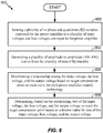
- FIG. 5 is a flowchart illustrating a method 500, in accordance with one or more exemplary embodiments.
- Method 500 may include calculating input voltage values and bias voltage values of a power amplifier for each desired output voltage value of the power amplifier at a desired compression point (depicted by numeral 502).
- method 500 may include calibrating a radio-frequency (RF) device including the power amplifier based on the calculated input and bias voltage values (depicted by numeral 504).
- RF radio-frequency
- FIG. 6 is a flowchart illustrating a method 600, in accordance with one or more exemplary embodiments.
- Method 600 may include sensing a plurality of IQ samples conveyed by the power amplifier at a plurality of input voltages and bias voltages conveyed to the power amplifier (depicted by numeral 602).
- method 600 may include generating a plurality of amplitude-to-amplitude (AM-AM) curves from the plurality of sensed IQ samples (depicted by numeral 604).
- Method 600 may also include determining a relationship among the input voltage, the bias voltage, and the output voltage based on target compression point on each curve for each power amplifier control technology (depicted by numeral 606).
- method 600 may include determining, based on the relationship, two of the input voltage, the bias voltage, and the output voltage to reach the target compression point based on a known value for one of the input voltage, bias voltage, and the output voltage (depicted by numeral 608).
- Exemplary embodiments of the present invention as disclosed herein enable the AM-AM on each power amplifier part to be determined. Further, there is no need for characterization, which may be required be conventional methods. In addition, exemplary embodiments provide for accurate identification of compression points, enhanced efficiency and accurate output power prediction after DPD. Moreover, exemplary embodiments may reduce calibration time as compared to conventional methods.
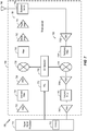
- FIG. 7 shows a block diagram of an exemplary design of a wireless communication device 700.
- wireless device 700 includes a data processor 710 and a transceiver 720.
- Transceiver 720 includes a transmitter 730 and a receiver 750 that support bi-directional wireless communication.
- wireless device 700 may include any number of transmitters and any number of receivers for any number of communication systems and any number of frequency bands.
- data processor 710 processes data to be transmitted and provides an analog output signal to transmitter 730.
- the analog output signal is amplified by an amplifier (Amp) 732, filtered by a lowpass filter 734 to remove images caused by digital-to-analog conversion, amplified by a VGA 736, and upconverted from baseband to RF by a mixer 738.
- the upconverted signal is filtered by a filter 740, further amplified by a driver amplifier 742 and a power amplifier 744, routed through switches/duplexers 746, and transmitted via an antenna 748.
- power amplifier 744 may comprise power amplifier 106 of FIG. 1 and/or power amplifier 214 of FIG. 2 .
- antenna 748 receives signals from base stations and/or other transmitter stations and provides a received signal, which is routed through switches/duplexers 746 and provided to receiver 750.
- the received signal is amplified by an LNA 752, filtered by a bandpass filter 754, and downconverted from RF to baseband by a mixer 756.
- the downconverted signal is amplified by a VGA 758, filtered by a lowpass filter 760, and amplified by an amplifier 762 to obtain an analog input signal, which is provided to data processor 710.
- FIG. 7 shows transmitter 730 and receiver 750 implementing a direct-conversion architecture, which frequency converts a signal between RF and baseband in one stage.
- Transmitter 730 and/or receiver 750 may also implement a super-heterodyne architecture, which frequency converts a signal between RF and baseband in multiple stages.
- a local oscillator (LO) generator 770 generates and provides transmit and receive LO signals to mixers 738 and 756, respectively.
- a phase locked loop (PLL) 772 receives control information from data processor 710 and provides control signals to LO generator 770 to generate the transmit and receive LO signals at the proper frequencies.
- LO local oscillator
- PLL phase locked loop
- FIG. 7 shows an exemplary transceiver design.
- the conditioning of the signals in transmitter 730 and receiver 750 may be performed by one or more stages of amplifier, filter, mixer, etc. These circuits may be arranged differently from the configuration shown in FIG. 7 .
- other circuits not shown in FIG. 7 may also be used in transmitter 730 and receiver 750.
- transmitter 730 may include a gain unit (e.g., post-DPD gain unit 208), an RF gain index (e.g., RF gain index 212), and/or a DPD unit (e.g., DPD unit 202).
- device 700 may include one or more matching circuits for matching various active circuits in FIG. 7 . Some circuits in FIG. 7 may also be omitted.
- transceiver 720 may be implemented on one or more analog integrated circuits (ICs), RF ICs (RFICs), mixed-signal ICs, etc.
- ICs analog integrated circuits
- RFICs RF ICs
- amplifier 732 through power amplifier 744 in transmitter 730 may be implemented on an RFIC.
- Driver amplifier 742 and power amplifier 744 may also be implemented on another IC external to the RFIC.
- Data processor 710 may perform various functions for wireless device 700, e.g., processing for transmitted and received data.
- Memory 712 may store program codes and data for data processor 710. More specifically, memory 712 may store program codes for execution by data processor 710 to carry out the methods described herein.
- Data processor 710 may be implemented on one or more application specific integrated circuits (ASICs) and/or other ICs.
- ASICs application specific integrated circuits
- DSP Digital Signal Processor
- ASIC Application Specific Integrated Circuit
- FPGA Field Programmable Gate Array
- a general purpose processor may be a microprocessor, but in the alternative, the processor may be any conventional processor, controller, microcontroller, or state machine.
- a processor may also be implemented as a combination of computing devices, e.g., a combination of a DSP and a microprocessor, a plurality of microprocessors, one or more microprocessors in conjunction with a DSP core, or any other such configuration.
- the functions described may be implemented in hardware, software, firmware, or any combination thereof. If implemented in software, the functions may be stored on or transmitted over as one or more instructions or code on a computer-readable medium.
- Computer-readable media includes both computer storage media and communication media including any medium that facilitates transfer of a computer program from one place to another.
- a storage media may be any available media that can be accessed by a computer.
- such computer-readable media can comprise RAM, ROM, EEPROM, CD-ROM or other optical disk storage, magnetic disk storage or other magnetic storage devices, or any other medium that can be used to carry or store desired program code in the form of instructions or data structures and that can be accessed by a computer.
- any connection is properly termed a computer-readable medium.
- the software is transmitted from a website, server, or other remote source using a coaxial cable, fiber optic cable, twisted pair, digital subscriber line (DSL), or wireless technologies such as infrared, radio, and microwave
- the coaxial cable, fiber optic cable, twisted pair, DSL, or wireless technologies such as infrared, radio, and microwave are included in the definition of medium.
- Disk and disc includes compact disc (CD), laser disc, optical disc, digital versatile disc (DVD), floppy disk and blu-ray disc where disks usually reproduce data magnetically, while discs reproduce data optically with lasers. Combinations of the above should also be included within the scope of computer-readable media.
Landscapes
- Engineering & Computer Science (AREA)
- Power Engineering (AREA)
- Physics & Mathematics (AREA)
- Nonlinear Science (AREA)
- Amplifiers (AREA)
Applications Claiming Priority (3)
| Application Number | Priority Date | Filing Date | Title |
|---|---|---|---|
| US201361805839P | 2013-03-27 | 2013-03-27 | |
| US14/205,265 US9729110B2 (en) | 2013-03-27 | 2014-03-11 | Radio-frequency device calibration |
| PCT/US2014/024913 WO2014159728A1 (en) | 2013-03-27 | 2014-03-12 | Radio-frequency device calibration |
Publications (2)
| Publication Number | Publication Date |
|---|---|
| EP2979357A1 EP2979357A1 (en) | 2016-02-03 |
| EP2979357B1 true EP2979357B1 (en) | 2017-05-31 |
Family
ID=51620191
Family Applications (1)
| Application Number | Title | Priority Date | Filing Date |
|---|---|---|---|
| EP14716147.5A Active EP2979357B1 (en) | 2013-03-27 | 2014-03-12 | Radio-frequency device calibration |
Country Status (6)
Families Citing this family (10)
| Publication number | Priority date | Publication date | Assignee | Title |
|---|---|---|---|---|
| US9565642B2 (en) * | 2014-04-11 | 2017-02-07 | Cree, Inc. | GaN amplifier for WiFi applications |
| CN106797356B (zh) * | 2014-12-29 | 2020-07-07 | 华为技术有限公司 | 一种数字预失真校正系数的控制方法及装置 |
| GB201613948D0 (en) * | 2016-08-15 | 2016-09-28 | Univ Surrey | Load modulation in signal transmission |
| US10756675B2 (en) * | 2018-11-28 | 2020-08-25 | Qorvo Us, Inc. | Broadband power amplifier circuit |
| US11515617B1 (en) | 2019-04-03 | 2022-11-29 | Micro Mobio Corporation | Radio frequency active antenna system in a package |
| CN111220897B (zh) * | 2020-02-11 | 2022-01-21 | 南京派格测控科技有限公司 | 功率校准方法、装置、系统以及测试系统 |
| CN112083370B (zh) * | 2020-08-25 | 2024-02-09 | 山东浪潮科学研究院有限公司 | 一种混频器直流偏置校准方法、设备及介质 |
| CN112422463B (zh) * | 2020-09-28 | 2023-02-03 | 山东浪潮科学研究院有限公司 | 一种直流偏置校准方法、设备及介质 |
| WO2023140827A1 (en) * | 2022-01-18 | 2023-07-27 | Zeku, Inc. | Apparatus and method for fast average power tracking calibration of a radio frequency chip |
| US20240429883A1 (en) * | 2023-06-23 | 2024-12-26 | Qualcomm Incorporated | Interpolated power tracking and input power adjustment based on peak-to-average power ratio |
Family Cites Families (19)
| Publication number | Priority date | Publication date | Assignee | Title |
|---|---|---|---|---|
| US6246286B1 (en) * | 1999-10-26 | 2001-06-12 | Telefonaktiebolaget Lm Ericsson | Adaptive linearization of power amplifiers |
| JP2002318256A (ja) * | 2001-04-24 | 2002-10-31 | Mitsubishi Electric Corp | 増幅器の総合特性計算装置 |
| US7058369B1 (en) | 2001-11-21 | 2006-06-06 | Pmc-Sierra Inc. | Constant gain digital predistortion controller for linearization of non-linear amplifiers |
| US6985704B2 (en) | 2002-05-01 | 2006-01-10 | Dali Yang | System and method for digital memorized predistortion for wireless communication |
| US6646501B1 (en) | 2002-06-25 | 2003-11-11 | Nortel Networks Limited | Power amplifier configuration |
| JP2005109860A (ja) * | 2003-09-30 | 2005-04-21 | Seiko Epson Corp | 回路特性調整装置 |
| US7915954B2 (en) * | 2004-01-16 | 2011-03-29 | Qualcomm, Incorporated | Amplifier predistortion and autocalibration method and apparatus |
| US7145390B2 (en) | 2004-09-03 | 2006-12-05 | Broadcom Corporation | Differential power amplifier and method in class AB mode |
| US20060199553A1 (en) * | 2005-03-07 | 2006-09-07 | Andrew Corporation | Integrated transceiver with envelope tracking |
| GB2434932B (en) | 2006-02-03 | 2010-11-10 | Filtronic Plc | Amplifier |
| US7957707B2 (en) | 2007-03-30 | 2011-06-07 | Freescale Semiconductor, Inc. | Systems, apparatus and method for performing digital pre-distortion based on lookup table gain values |
| US7564311B2 (en) * | 2007-09-28 | 2009-07-21 | Intel Corporation | Method and apparatus to enhance linearity and efficiency in an RF power amplifier |
| CN101247153B (zh) | 2008-03-13 | 2011-11-30 | 中兴通讯股份有限公司 | 一种提升功放效率的方法及其数字预失真宽带发信机 |
| US8620233B2 (en) | 2008-04-11 | 2013-12-31 | Samsung Electroncs Co., Ltd. | Method of power amplifier predistortion adaptation using compression detection |
| US8433263B2 (en) * | 2008-09-24 | 2013-04-30 | Freescale Semiconductor, Inc. | Wireless communication unit, integrated circuit and method of power control of a power amplifier therefor |
| US7777566B1 (en) | 2009-02-05 | 2010-08-17 | Quantance, Inc. | Amplifier compression adjustment circuit |
| JP5206526B2 (ja) | 2009-03-19 | 2013-06-12 | 富士通株式会社 | 増幅装置および送信装置 |
| US8912851B2 (en) * | 2010-12-30 | 2014-12-16 | Intel Mobile Communications GmbH | Apparatus and method for providing amplifier linearity information |
| US9041464B2 (en) | 2011-09-16 | 2015-05-26 | Qualcomm Incorporated | Circuitry for reducing power consumption |
-
2014
- 2014-03-11 US US14/205,265 patent/US9729110B2/en not_active Expired - Fee Related
- 2014-03-12 EP EP14716147.5A patent/EP2979357B1/en active Active
- 2014-03-12 CN CN201480018544.9A patent/CN105075112A/zh active Pending
- 2014-03-12 KR KR1020157030397A patent/KR20150135421A/ko not_active Withdrawn
- 2014-03-12 JP JP2016505480A patent/JP6337087B2/ja not_active Expired - Fee Related
- 2014-03-12 WO PCT/US2014/024913 patent/WO2014159728A1/en active Application Filing
Also Published As
| Publication number | Publication date |
|---|---|
| JP2016514918A (ja) | 2016-05-23 |
| JP6337087B2 (ja) | 2018-06-06 |
| EP2979357A1 (en) | 2016-02-03 |
| KR20150135421A (ko) | 2015-12-02 |
| US9729110B2 (en) | 2017-08-08 |
| US20140292404A1 (en) | 2014-10-02 |
| WO2014159728A1 (en) | 2014-10-02 |
| CN105075112A (zh) | 2015-11-18 |
Similar Documents
| Publication | Publication Date | Title |
|---|---|---|
| EP2979357B1 (en) | Radio-frequency device calibration | |
| US9680422B2 (en) | Power amplifier signal compensation | |
| US20150194936A1 (en) | Power amplifier envelope tracking | |
| EP3031135B1 (en) | Analog switch for rf front end | |
| US10567092B2 (en) | System to calibrate phase using system information | |
| US9142877B2 (en) | Control of a transmitter output power | |
| KR101521186B1 (ko) | 온도 보상을 갖는 전력 검출기 | |
| JP4802190B2 (ja) | ポーラ変調送信回路及び通信機器 | |
| US20110025414A1 (en) | Predistortion of amplifier input signals | |
| US20120326686A1 (en) | Power supply generator with noise cancellation | |
| EP2449675B1 (en) | Gain control linearity in an rf driver amplifier transmitter | |
| KR101309856B1 (ko) | 자체 진단 트랜스시버 아키텍처 및 관련된 방법 | |
| US20140111252A1 (en) | Threshold tracking bias voltage for mixers | |
| CN101479946B (zh) | 发送电路及通信设备 | |
| EP2590346B1 (en) | High-frequency signal processor and wireless communication system | |
| US9100842B2 (en) | Apparatus and method for supporting calibration for radio frequency circuit in communication device | |
| US7889810B2 (en) | Method and apparatus for a nonlinear feedback control system | |
| US20170302229A1 (en) | Amplification device | |
| SUBHARMONIC | c12) United States Patent |
Legal Events
| Date | Code | Title | Description |
|---|---|---|---|
| PUAI | Public reference made under article 153(3) epc to a published international application that has entered the european phase |
Free format text: ORIGINAL CODE: 0009012 |
|
| 17P | Request for examination filed |
Effective date: 20150825 |
|
| AK | Designated contracting states |
Kind code of ref document: A1 Designated state(s): AL AT BE BG CH CY CZ DE DK EE ES FI FR GB GR HR HU IE IS IT LI LT LU LV MC MK MT NL NO PL PT RO RS SE SI SK SM TR |
|
| AX | Request for extension of the european patent |
Extension state: BA ME |
|
| DAX | Request for extension of the european patent (deleted) | ||
| REG | Reference to a national code |
Ref country code: DE Ref legal event code: R079 Ref document number: 602014010278 Country of ref document: DE Free format text: PREVIOUS MAIN CLASS: H03F0001020000 Ipc: H03F0003189000 |
|
| GRAP | Despatch of communication of intention to grant a patent |
Free format text: ORIGINAL CODE: EPIDOSNIGR1 |
|
| RIC1 | Information provided on ipc code assigned before grant |
Ipc: H03F 1/32 20060101ALI20161123BHEP Ipc: H03F 3/189 20060101AFI20161123BHEP Ipc: H03F 1/02 20060101ALI20161123BHEP Ipc: H03F 3/20 20060101ALI20161123BHEP |
|
| INTG | Intention to grant announced |
Effective date: 20161213 |
|
| GRAS | Grant fee paid |
Free format text: ORIGINAL CODE: EPIDOSNIGR3 |
|
| GRAA | (expected) grant |
Free format text: ORIGINAL CODE: 0009210 |
|
| AK | Designated contracting states |
Kind code of ref document: B1 Designated state(s): AL AT BE BG CH CY CZ DE DK EE ES FI FR GB GR HR HU IE IS IT LI LT LU LV MC MK MT NL NO PL PT RO RS SE SI SK SM TR |
|
| REG | Reference to a national code |
Ref country code: CH Ref legal event code: EP Ref country code: GB Ref legal event code: FG4D |
|
| REG | Reference to a national code |
Ref country code: AT Ref legal event code: REF Ref document number: 898268 Country of ref document: AT Kind code of ref document: T Effective date: 20170615 |
|
| REG | Reference to a national code |
Ref country code: IE Ref legal event code: FG4D |
|
| REG | Reference to a national code |
Ref country code: DE Ref legal event code: R096 Ref document number: 602014010278 Country of ref document: DE |
|
| REG | Reference to a national code |
Ref country code: NL Ref legal event code: MP Effective date: 20170531 |
|
| REG | Reference to a national code |
Ref country code: LT Ref legal event code: MG4D |
|
| REG | Reference to a national code |
Ref country code: AT Ref legal event code: MK05 Ref document number: 898268 Country of ref document: AT Kind code of ref document: T Effective date: 20170531 |
|
| PG25 | Lapsed in a contracting state [announced via postgrant information from national office to epo] |
Ref country code: NO Free format text: LAPSE BECAUSE OF FAILURE TO SUBMIT A TRANSLATION OF THE DESCRIPTION OR TO PAY THE FEE WITHIN THE PRESCRIBED TIME-LIMIT Effective date: 20170831 Ref country code: AT Free format text: LAPSE BECAUSE OF FAILURE TO SUBMIT A TRANSLATION OF THE DESCRIPTION OR TO PAY THE FEE WITHIN THE PRESCRIBED TIME-LIMIT Effective date: 20170531 Ref country code: ES Free format text: LAPSE BECAUSE OF FAILURE TO SUBMIT A TRANSLATION OF THE DESCRIPTION OR TO PAY THE FEE WITHIN THE PRESCRIBED TIME-LIMIT Effective date: 20170531 Ref country code: GR Free format text: LAPSE BECAUSE OF FAILURE TO SUBMIT A TRANSLATION OF THE DESCRIPTION OR TO PAY THE FEE WITHIN THE PRESCRIBED TIME-LIMIT Effective date: 20170901 Ref country code: HR Free format text: LAPSE BECAUSE OF FAILURE TO SUBMIT A TRANSLATION OF THE DESCRIPTION OR TO PAY THE FEE WITHIN THE PRESCRIBED TIME-LIMIT Effective date: 20170531 Ref country code: FI Free format text: LAPSE BECAUSE OF FAILURE TO SUBMIT A TRANSLATION OF THE DESCRIPTION OR TO PAY THE FEE WITHIN THE PRESCRIBED TIME-LIMIT Effective date: 20170531 Ref country code: LT Free format text: LAPSE BECAUSE OF FAILURE TO SUBMIT A TRANSLATION OF THE DESCRIPTION OR TO PAY THE FEE WITHIN THE PRESCRIBED TIME-LIMIT Effective date: 20170531 |
|
| PG25 | Lapsed in a contracting state [announced via postgrant information from national office to epo] |
Ref country code: LV Free format text: LAPSE BECAUSE OF FAILURE TO SUBMIT A TRANSLATION OF THE DESCRIPTION OR TO PAY THE FEE WITHIN THE PRESCRIBED TIME-LIMIT Effective date: 20170531 Ref country code: NL Free format text: LAPSE BECAUSE OF FAILURE TO SUBMIT A TRANSLATION OF THE DESCRIPTION OR TO PAY THE FEE WITHIN THE PRESCRIBED TIME-LIMIT Effective date: 20170531 Ref country code: RS Free format text: LAPSE BECAUSE OF FAILURE TO SUBMIT A TRANSLATION OF THE DESCRIPTION OR TO PAY THE FEE WITHIN THE PRESCRIBED TIME-LIMIT Effective date: 20170531 Ref country code: BG Free format text: LAPSE BECAUSE OF FAILURE TO SUBMIT A TRANSLATION OF THE DESCRIPTION OR TO PAY THE FEE WITHIN THE PRESCRIBED TIME-LIMIT Effective date: 20170831 Ref country code: SE Free format text: LAPSE BECAUSE OF FAILURE TO SUBMIT A TRANSLATION OF THE DESCRIPTION OR TO PAY THE FEE WITHIN THE PRESCRIBED TIME-LIMIT Effective date: 20170531 Ref country code: IS Free format text: LAPSE BECAUSE OF FAILURE TO SUBMIT A TRANSLATION OF THE DESCRIPTION OR TO PAY THE FEE WITHIN THE PRESCRIBED TIME-LIMIT Effective date: 20170930 |
|
| PG25 | Lapsed in a contracting state [announced via postgrant information from national office to epo] |
Ref country code: RO Free format text: LAPSE BECAUSE OF FAILURE TO SUBMIT A TRANSLATION OF THE DESCRIPTION OR TO PAY THE FEE WITHIN THE PRESCRIBED TIME-LIMIT Effective date: 20170531 Ref country code: CZ Free format text: LAPSE BECAUSE OF FAILURE TO SUBMIT A TRANSLATION OF THE DESCRIPTION OR TO PAY THE FEE WITHIN THE PRESCRIBED TIME-LIMIT Effective date: 20170531 Ref country code: DK Free format text: LAPSE BECAUSE OF FAILURE TO SUBMIT A TRANSLATION OF THE DESCRIPTION OR TO PAY THE FEE WITHIN THE PRESCRIBED TIME-LIMIT Effective date: 20170531 Ref country code: EE Free format text: LAPSE BECAUSE OF FAILURE TO SUBMIT A TRANSLATION OF THE DESCRIPTION OR TO PAY THE FEE WITHIN THE PRESCRIBED TIME-LIMIT Effective date: 20170531 Ref country code: SK Free format text: LAPSE BECAUSE OF FAILURE TO SUBMIT A TRANSLATION OF THE DESCRIPTION OR TO PAY THE FEE WITHIN THE PRESCRIBED TIME-LIMIT Effective date: 20170531 |
|
| REG | Reference to a national code |
Ref country code: FR Ref legal event code: PLFP Year of fee payment: 5 |
|
| PG25 | Lapsed in a contracting state [announced via postgrant information from national office to epo] |
Ref country code: PL Free format text: LAPSE BECAUSE OF FAILURE TO SUBMIT A TRANSLATION OF THE DESCRIPTION OR TO PAY THE FEE WITHIN THE PRESCRIBED TIME-LIMIT Effective date: 20170531 Ref country code: IT Free format text: LAPSE BECAUSE OF FAILURE TO SUBMIT A TRANSLATION OF THE DESCRIPTION OR TO PAY THE FEE WITHIN THE PRESCRIBED TIME-LIMIT Effective date: 20170531 Ref country code: SM Free format text: LAPSE BECAUSE OF FAILURE TO SUBMIT A TRANSLATION OF THE DESCRIPTION OR TO PAY THE FEE WITHIN THE PRESCRIBED TIME-LIMIT Effective date: 20170531 |
|
| REG | Reference to a national code |
Ref country code: DE Ref legal event code: R097 Ref document number: 602014010278 Country of ref document: DE |
|
| PLBE | No opposition filed within time limit |
Free format text: ORIGINAL CODE: 0009261 |
|
| STAA | Information on the status of an ep patent application or granted ep patent |
Free format text: STATUS: NO OPPOSITION FILED WITHIN TIME LIMIT |
|
| 26N | No opposition filed |
Effective date: 20180301 |
|
| PG25 | Lapsed in a contracting state [announced via postgrant information from national office to epo] |
Ref country code: SI Free format text: LAPSE BECAUSE OF FAILURE TO SUBMIT A TRANSLATION OF THE DESCRIPTION OR TO PAY THE FEE WITHIN THE PRESCRIBED TIME-LIMIT Effective date: 20170531 |
|
| REG | Reference to a national code |
Ref country code: CH Ref legal event code: PL |
|
| PG25 | Lapsed in a contracting state [announced via postgrant information from national office to epo] |
Ref country code: MC Free format text: LAPSE BECAUSE OF FAILURE TO SUBMIT A TRANSLATION OF THE DESCRIPTION OR TO PAY THE FEE WITHIN THE PRESCRIBED TIME-LIMIT Effective date: 20170531 |
|
| REG | Reference to a national code |
Ref country code: BE Ref legal event code: MM Effective date: 20180331 |
|
| REG | Reference to a national code |
Ref country code: IE Ref legal event code: MM4A |
|
| PG25 | Lapsed in a contracting state [announced via postgrant information from national office to epo] |
Ref country code: LU Free format text: LAPSE BECAUSE OF NON-PAYMENT OF DUE FEES Effective date: 20180312 |
|
| PG25 | Lapsed in a contracting state [announced via postgrant information from national office to epo] |
Ref country code: IE Free format text: LAPSE BECAUSE OF NON-PAYMENT OF DUE FEES Effective date: 20180312 |
|
| PG25 | Lapsed in a contracting state [announced via postgrant information from national office to epo] |
Ref country code: BE Free format text: LAPSE BECAUSE OF NON-PAYMENT OF DUE FEES Effective date: 20180331 Ref country code: LI Free format text: LAPSE BECAUSE OF NON-PAYMENT OF DUE FEES Effective date: 20180331 Ref country code: CH Free format text: LAPSE BECAUSE OF NON-PAYMENT OF DUE FEES Effective date: 20180331 |
|
| PG25 | Lapsed in a contracting state [announced via postgrant information from national office to epo] |
Ref country code: MT Free format text: LAPSE BECAUSE OF NON-PAYMENT OF DUE FEES Effective date: 20180312 |
|
| PG25 | Lapsed in a contracting state [announced via postgrant information from national office to epo] |
Ref country code: TR Free format text: LAPSE BECAUSE OF FAILURE TO SUBMIT A TRANSLATION OF THE DESCRIPTION OR TO PAY THE FEE WITHIN THE PRESCRIBED TIME-LIMIT Effective date: 20170531 |
|
| PG25 | Lapsed in a contracting state [announced via postgrant information from national office to epo] |
Ref country code: PT Free format text: LAPSE BECAUSE OF FAILURE TO SUBMIT A TRANSLATION OF THE DESCRIPTION OR TO PAY THE FEE WITHIN THE PRESCRIBED TIME-LIMIT Effective date: 20170531 |
|
| PG25 | Lapsed in a contracting state [announced via postgrant information from national office to epo] |
Ref country code: MK Free format text: LAPSE BECAUSE OF NON-PAYMENT OF DUE FEES Effective date: 20170531 Ref country code: CY Free format text: LAPSE BECAUSE OF FAILURE TO SUBMIT A TRANSLATION OF THE DESCRIPTION OR TO PAY THE FEE WITHIN THE PRESCRIBED TIME-LIMIT Effective date: 20170531 Ref country code: HU Free format text: LAPSE BECAUSE OF FAILURE TO SUBMIT A TRANSLATION OF THE DESCRIPTION OR TO PAY THE FEE WITHIN THE PRESCRIBED TIME-LIMIT; INVALID AB INITIO Effective date: 20140312 |
|
| PG25 | Lapsed in a contracting state [announced via postgrant information from national office to epo] |
Ref country code: AL Free format text: LAPSE BECAUSE OF FAILURE TO SUBMIT A TRANSLATION OF THE DESCRIPTION OR TO PAY THE FEE WITHIN THE PRESCRIBED TIME-LIMIT Effective date: 20170531 |
|
| PGFP | Annual fee paid to national office [announced via postgrant information from national office to epo] |
Ref country code: DE Payment date: 20250210 Year of fee payment: 12 |
|
| PGFP | Annual fee paid to national office [announced via postgrant information from national office to epo] |
Ref country code: FR Payment date: 20250211 Year of fee payment: 12 |
|
| PGFP | Annual fee paid to national office [announced via postgrant information from national office to epo] |
Ref country code: GB Payment date: 20250213 Year of fee payment: 12 |