EP2978290A2 - Sensorkopf für einen flugkörper - Google Patents
Sensorkopf für einen flugkörper Download PDFInfo
- Publication number
- EP2978290A2 EP2978290A2 EP15001998.2A EP15001998A EP2978290A2 EP 2978290 A2 EP2978290 A2 EP 2978290A2 EP 15001998 A EP15001998 A EP 15001998A EP 2978290 A2 EP2978290 A2 EP 2978290A2
- Authority
- EP
- European Patent Office
- Prior art keywords
- sensor head
- housing
- electronics
- sensor
- electronics housing
- Prior art date
- Legal status (The legal status is an assumption and is not a legal conclusion. Google has not performed a legal analysis and makes no representation as to the accuracy of the status listed.)
- Granted
Links
Images


Classifications
-
- H—ELECTRICITY
- H05—ELECTRIC TECHNIQUES NOT OTHERWISE PROVIDED FOR
- H05K—PRINTED CIRCUITS; CASINGS OR CONSTRUCTIONAL DETAILS OF ELECTRIC APPARATUS; MANUFACTURE OF ASSEMBLAGES OF ELECTRICAL COMPONENTS
- H05K7/00—Constructional details common to different types of electric apparatus
- H05K7/14—Mounting supporting structure in casing or on frame or rack
- H05K7/1422—Printed circuit boards receptacles, e.g. stacked structures, electronic circuit modules or box like frames
- H05K7/1427—Housings
- H05K7/1434—Housings for electronics exposed to high gravitational force; Cylindrical housings
-
- F—MECHANICAL ENGINEERING; LIGHTING; HEATING; WEAPONS; BLASTING
- F41—WEAPONS
- F41G—WEAPON SIGHTS; AIMING
- F41G7/00—Direction control systems for self-propelled missiles
- F41G7/20—Direction control systems for self-propelled missiles based on continuous observation of target position
- F41G7/22—Homing guidance systems
- F41G7/2253—Passive homing systems, i.e. comprising a receiver and do not requiring an active illumination of the target
-
- F—MECHANICAL ENGINEERING; LIGHTING; HEATING; WEAPONS; BLASTING
- F41—WEAPONS
- F41G—WEAPON SIGHTS; AIMING
- F41G7/00—Direction control systems for self-propelled missiles
- F41G7/20—Direction control systems for self-propelled missiles based on continuous observation of target position
- F41G7/22—Homing guidance systems
- F41G7/2273—Homing guidance systems characterised by the type of waves
- F41G7/2293—Homing guidance systems characterised by the type of waves using electromagnetic waves other than radio waves
-
- H—ELECTRICITY
- H05—ELECTRIC TECHNIQUES NOT OTHERWISE PROVIDED FOR
- H05K—PRINTED CIRCUITS; CASINGS OR CONSTRUCTIONAL DETAILS OF ELECTRIC APPARATUS; MANUFACTURE OF ASSEMBLAGES OF ELECTRICAL COMPONENTS
- H05K7/00—Constructional details common to different types of electric apparatus
- H05K7/20—Modifications to facilitate cooling, ventilating, or heating
- H05K7/2039—Modifications to facilitate cooling, ventilating, or heating characterised by the heat transfer by conduction from the heat generating element to a dissipating body
- H05K7/20436—Inner thermal coupling elements in heat dissipating housings, e.g. protrusions or depressions integrally formed in the housing
- H05K7/20445—Inner thermal coupling elements in heat dissipating housings, e.g. protrusions or depressions integrally formed in the housing the coupling element being an additional piece, e.g. thermal standoff
Definitions
- the invention relates to a sensor head for a missile, with a sensor head housing, an electronics unit and an electronics housing around the electronics unit.
- Missiles often have a sensor head for measuring size measurement in the bow region of their fuselage. This measured variable detection usually takes place by means of an electronic unit arranged in the sensor head and serves to guide the target of the missile.
- an electronics unit usually comprises a number of boards, which are each equipped with a number of electronic components.
- the sensor head may experience extreme accelerations and high speeds. This is especially the case with precision ammunition, such as a guided artillery round.
- the accelerations occurring there can be up to 26,000 g at launch.
- a reliable function of the electronic unit is necessary even under such extreme conditions.
- the electronic unit has, inter alia, an electronics housing with a cavity and two superimposed, supported by so-called. Support structures boards.
- the housing is prepared to be fitted in a sensor head housing.
- the electronics housing has an outer contour corresponding to the inner contour of the sensor head housing.
- a sensor head of the aforementioned type in which, according to the invention, the electronics housing at least predominantly encloses the electronics unit and has an essentially rotationally symmetrical outer contour and arranged in a rotationally parallel to the axis formed by the sensor head housing substantially rotational axis, wherein a thermal insulation layer between the electronics housing and the sensor head housing is arranged.
- the invention is based on the consideration that missiles, such as long-range shot tube ammunition fly over long distances at high speeds through the atmosphere. In this case, air friction temperatures of 250 ° C and above may occur at the missile bow.
- the maximum permissible temperature of electronic components of the electronics unit is usually only 100 ° C.
- the function of the electronic unit - and thus for example the precise guidance of the missile - can be affected by the frictional heat during flight of the missile at high speed. This may be the case, in particular, when the sensor head has a comparatively large contact area between the housing of the electronics unit and the housing of the sensor head as a thermal bridge.
- the heat conduction between the two housings is favored, so that the frictional heat penetrate to the electronics unit, this heat unduly high and consequently can affect up to the failure of function.
- this heat conduction can be reduced, thus reducing the heating of the electronics unit by the frictional heat and consequently a failure of the electronics unit can be avoided by overheating.
- the invention is particularly advantageous applicable to a missile, designed as precision ammunition, in particular designed as a guided artillery shell.
- the frictional heat due to the high airspeed of up to 1 km / s is particularly high, so that the thermal insulation layer can particularly effectively reduce the risk of failure of the electronics unit due to overheating.
- the sensor head housing may be prepared for mounting on the fuselage of a missile or may be adapted to form the fuselage nose of a missile.
- the substantially rotationally symmetrical cavity formed by the sensor head housing may have a tubular, cylindrical and / or conical shape.
- the electronics unit comprises at least one circuit board or a printed circuit board with a plurality of electronic components, in particular optoelectronic components.
- the electronics unit is prepared for at least predominantly performing a function, for example an opto-electronic target detection function for the guidance of the missile.
- the electronics housing is in particular arranged coaxially in the sensor head housing, so that a swirl-related imbalance is reduced during flight of the missile.
- the substantially rotationally symmetrical outer contour of the electronics housing can essentially have a tubular, cylindrical and / or conical shape.
- the thermal insulation layer is in particular arranged radially between the electronics housing and the sensor head housing.
- the thermal insulation layer may be disposed in or formed by a gap between the electronics housing and the sensor head housing.
- the insulation layer is formed by a radial air gap between the electronics housing and the sensor head housing of at least 1%, preferably at least 2%, of the maximum diameter of the electronics housing.
- the air gap dimension can be realized by a suitable dimensioning of the outer diameter of the electronics housing and the inner diameter of the sensor head housing with simple means with a predetermined value.
- the radial air gap has a measure determined for the purpose of effective thermal insulation.
- the air gap is technically significantly different from a tolerance-related, unwanted play between the electronics housing and the sensor head housing, which should not exceed 50 microns in missiles, in particular missile-resistant missiles.
- a gap of at least 0.2 mm, in particular of at least 0.5 mm is advantageous.
- a solid, plastic or castable insulating material can form at least part of the insulating layer.
- a material forming the thermal insulation layer can be prepared for pouring into the gap and in particular for at least predominantly filling in the gap.
- the insulation layer extends in the tangential direction circumferentially over at least 270 °, preferably over more than 330 °, to the electronics housing.
- the insulation layer extends in the axial direction over at least half, in particular at least 80%, of the axial length of the electronics housing.
- the insulation layer may extend in sections in the axial direction, that is to say consisting of a plurality of separate insulation layer sections, over the electronics housing.
- a remaining thermal bridge between sensor head and electronics housing is expediently arranged in a region within which no or only individual, temperature-resistant electronic components are arranged.
- a particularly effective thermal insulation of the electronics unit can be achieved if the insulating layer encases an at least predominant proportion, in particular more than 80%, of the outer surface of the electronics housing.
- This can be achieved in a particularly simple manner if the electronics housing is fastened at least predominantly on one of its end faces in the sensor head housing so that the remaining outer surface of the electronics housing is at least predominantly non-contact with the inner surface of the sensor head housing.
- the electronics housing is plugged at its bow-side end in a socket in the sensor head housing, wherein the outer surface of the electronics housing is radially fixed at a predetermined distance from the inner surface of the sensor head housing.
- the electronics housing has an opening extending over at least a predominant portion of the axial length of the electronics housing.
- This opening may be designed as a slot, a recess, an omission or a gap.
- the opening causes the electronics unit is partially not enclosed by the electronics housing, so that the electronic unit can at least partially adjacent to the insulating layer.
- the opening may be designed such that the insulation layer extends into the interior of the electronics housing.
- the insulation layer as an air gap is executed, formed by the opening in the region of the opening a radially recessed air gap, so that convection and / or improved insulation effect can be achieved.
- the electronics housing may have a plurality, in particular two, of such openings.
- the opening is a gap between two separate housing segment shells.
- the opening can be produced in this way low cost, since additional manufacturing steps for introducing the opening, for example, by a machining of the electronics housing, can be dispensed with.
- several gaps are provided at regular intervals over the circumference of the electronics housing.
- the gap has a tangential opening angle of at least 30 °, preferably 60 °.
- a comparatively large opening is achieved, so that the insulating layer, ie in particular the air gap, can better reach the components of the electronic unit.
- the electronic unit has a plurality of plates arranged one above the other in the axial direction, it can be achieved that the air of the air gap can circulate between the boards. By this circulation of the air gap, a convection-induced cooling effect can be achieved, whereby overheating of the electronic unit can be counteracted.
- the electronics housing has at least one housing segment shell with an internally formed circular arc-shaped tangential groove and a circular-cylindrical outer surface.
- a board or generally an electronics carrier may be introduced, which is hereinafter also referred to as a board for the sake of simplicity.
- the outer surface of the housing segment shell can be substantially cylindrical and extend tangentially over at least 90 °, preferably 120 °.
- at least two housing segment shells form the electronics housing at least partially.
- the housing segment shells can be arranged on opposite sides of the electronics unit and comprise them like a jaw.
- a plurality of housing segment shells are arranged at regular intervals over the circumference of the electronics unit. So can A balancing of the missile when taxiing during the flight are avoided.
- the invention is also directed to a sensor head of the type mentioned, in which the electronics unit according to the invention in at least three parallel planes - arranged axially one above the other - a first, a second and at least a third board, a first flexible flat cable, the first with the second board connects electrically conductive, a second flexible flat cable connects the second electrically conductively connected to the third board and the two flexible flat cable in the axial direction meandering the boards are arranged connecting.
- a meandering arrangement can be achieved when the first and second flexible flat cables are arranged at opposite edges of the second boards. are and in particular arcuately curved in opposite directions. Due to the curvature, the flexible flat cables have a length greater than necessary for bridging the board spacing.
- this meandering cable connection it is possible to ensure that the printed circuit boards of the electronics unit, insofar as they are not yet firmly mounted in the electronics housing, are largely axially movable relative to one another. In particular, such an accordion-like movement of the boards can be achieved, wherein an unwanted release of the electrically conductive connection is counteracted by the flexible, meandering connection.
- the assembly of the electronics unit in the electronics housing can therefore be realized low cost. A precise and thus usually complex production of the electronics housing, in particular the prepared for receiving the boards Tangentialnuten can also be avoided, since this type of flat cable assembly can compensate for distance tolerances.
- the invention is also directed to a sensor head of the aforementioned type, which according to the invention comprises a sensor optics with at least one optical element and a sensor disposed at an axial distance to the optical element, wherein the axial distance through an at least indirectly between the optical element and the sensor inserted axial distance adjustment element is adjusted.
- the sensor optics can be prepared for optical detection of targets of the missile.
- the optical element of the sensor optics is in particular an optical lens or an objective.
- the optical element can be in an optical storage, for example, the Recording and version of a lens is prepared to be stored.
- the optical element may be a part of the electronic unit.
- the sensor may be an optoelectronic detector.
- the sensor may be a part of the electronic unit, in particular an electronic component mounted on a board of the electronic unit.
- the sensor can be mounted in a sensor bearing.
- the axial distance between the optical element and the sensor may be a certain distance, which is necessary to achieve a function of the sensor head, in particular an opto-electronic target detection.
- the Axialabstandsjustageelement can be inserted between the optical element and the sensor in the sensor head, so that the distance between the optical element and the sensor adjusted by the Axialabstandsjustageelement, so is set.
- the Axialabstandsjustageelement may be a ring, a perforated disc, a plate with an opening or the like.
- the Axialabstandsjustageelement between the sensor bearing and the optical bearing is inserted into the sensor head.
- the optical element is mounted in the sensor head housing.
- the sensor head housing may for this purpose have a corresponding socket or holder for an optical lens.
- the optical element is mounted in the electronics housing.
- the electronics housing may for this purpose have a socket or a holder in which the optical element is arranged.
- the invention is directed to a sensor head of the aforementioned type.
- the sensor head provides an interface element arranged at an axial distance from an edge of the electronics housing, wherein the axial distance is adjusted by an at least indirectly inserted between the interface element and the electronics housing Axialabstandsjustageelement.
- the edge of the electronics housing is expediently an edge forming the rear end of the electronics housing.
- the interface element is, for example, a plug which is prepared for producing a plug connection with a plug coupling.
- the interface element can be prepared for the conduction of electrical signals that serve to guide the missile.
- it is necessary that the interface element is arranged at a certain axial distance from the edge of the electronics housing or that the interface element protrudes by a certain axial distance beyond the rear edge of the sensor head housing.
- the Axialabstandsjustageelement may be a ring, a perforated disc or a plate with an opening. For example, the Axialabstandsjustageelement between an interface member carrying board and a wall of the electronics housing is inserted.
- the invention is directed to a system of a plurality of sensor heads according to the invention, wherein each arranged at the same point Axialabstandsjustage implant the sensor heads have an axial thickness difference of at least 0.2 mm, preferably at least 0.7 mm.
- Each of the sensor heads of the system has at least one axial pitch adjustment element.
- the Axialabstandsjustage implant of the system are each arranged in the same place, so for example between the optical element and the sensor.
- the axial thickness difference is due to the purpose of pitch adjustment, which typically requires a different axial thickness of the axial pitch adjustment member for each sensor head of the system.
- an axial thickness difference of at least 0.2 mm, preferably 0.7 mm is sufficient for the purpose of appropriate axial distance adjustment for a large number of sensor heads. In some cases, it may be advantageous to provide an axial thickness difference of more than 1 mm, for example 2 mm.
- a further advantageous embodiment provides a supporting element which is supported in the electronics housing and which is arranged to support the back of a central region of a printed circuit board of the electronics unit in the axial direction.
- the support member may be a brace, a plate or a beam which is mounted in the electronics housing.
- the board is at least partially with its central region on the support element.
- the board can be a circular disk.
- the support element is a support wall and is arranged in the axial direction between two boards of the electronics unit and consists at least predominantly of metal.
- the arrangement between the two boards and the metallic material can be done in a simple manner an electromagnetic shielding of at least one of the boards of an electromagnetic influence by the other of the two boards. Due to the dual function of the support wall, namely the support at a start and the shield against radiation, these functions can be particularly low cost with a means - namely the support wall - can be achieved.
- the invention is directed to a method for mounting a sensor head.
- the method provides that, according to the invention, a difference between a desired value and an actual value of an axial distance between two elements of the sensor head is determined.
- the setpoint may be a value of an axial distance to an adjustment, in particular an in-focus, of the focus of the lens on the sensor.
- the elements can be a lens and a sensor.
- a deviation of the actual value of the distance from the desired value of the distance can result from an inevitably imperfect production.
- the difference between the setpoint and the actual value can be determined by a measurement or a gauge.
- an axial distance adjusting element having a certain axial thickness is selected from a set of Axial distance adjustment elements with different axial thicknesses selected.
- the set of axial spacing adjusting elements may comprise a plurality of elements whose axial thicknesses may differ from one another by up to 0.2 mm, in particular by up to 2 mm.
- the so selected Axialabstandsjustageelement is mounted in the sensor head and hereby adjusted the axial distance between the lens and the sensor. In this way, the required distance can be achieved at low cost while avoiding a complex precise production or a costly reworking on the sensor head.
- the two elements are an interface element and an edge of an electronics housing of the sensor head.
- the desired value may be a value required for the manufacturability of an interface connection, in particular a plug connection.
- the actual value of the distance results from the necessarily imperfect production or from tolerances of the interface element.
- the difference between the setpoint and the actual value can be determined by a measurement or a gauge.
- the so selected Axialabstandsjustageelement is mounted in the sensor head and hereby adjusted the axial distance between the interface element and the edge of the electronics housing. In this way, this required distance can be achieved at low cost while avoiding a complex precise production or a costly reworking on the sensor head.
- the invention is directed to a method for mounting a sensor head, in which a portion of a peripheral edge of a board of an electronics unit is inserted into a groove of a housing segment shell of an electronics housing.
- the peripheral edge of the board may be circular arc, in particular circular.
- the groove may be circular arc.
- the groove may be dimensioned in the thickness direction so that a frictional connection between the housing segment shell and the board is achieved.
- the housing segment shell may have a plurality of grooves for receiving a plurality of boards. It may be possible to insert more than one board in a groove.
- a further housing segment shell provided with a further groove is attached with this further groove to a further portion of the peripheral edge of the board.
- the housing segment shell on the first housing segment shell opposite peripheral edge or at a peripheral peripheral edge on the opposite side plugged so that the board is gripped like a jaw by the two housing segment shells.
- the board is fixed by the housing segment shells in the radial direction between them and hereby at least a part of the electronics unit - namely the board - mounted in the electronics housing. Due to the described plug connection between several, in particular two, housing segment shells, the electronics unit is particularly easy to install in the electronics housing. Furthermore, the board or its electronic components are easily accessible by merely removing one of the housing segment shells, which may be advantageous, for example, for removing and replacing an electronic component.
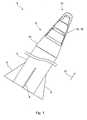
- FIG. 1 shows a schematic representation of a missile 2 with a fuselage 4 with rear side formed wings 6, a sensor head 8 and a hood 10.
- the hood 10 is shown in a longitudinal section and forms the foremost part of the missile in a direction of flight 2.
- the sensor head 8 has a rotationally symmetrical sensor head housing 14 and an optical element 16, which is embodied in the present embodiment as an optical lens 18.
- the sensor head 8 is for detecting targets and / or for guidance of the missile 2 by means of the optical element 16 and an electronics unit 22 mounted in the interior of the sensor head housing 14 (see FIG FIG. 2 ) prepared.
- the hood 10 is attached to the sensor head housing 14 and covers in particular the optical element 16 and the optical lens 18 for protection against damage.
- the missile 2 is designed as a guided artillery shell, so that the airspeed of the missile 2 is up to 1 km / s.
- high temperatures of up to 300 ° C. occur on the outer surface of the missile 2, in particular on the foremost region of the missile 2 or its bow.
- the hood 10 is usually the thermally most highly stressed by the air friction component of the missile. 2
- the hood 10 is prepared for dropping at a given time during a flight of the missile 2, so that the sensor head 8 after this predetermined time until the arrival of the missile 2 in a target forms the foremost region of the missile 2.
- the sensor head housing 14 is thermally highly stressed from this predetermined time by the applied frictional heat.
- the frictional heat is transported by the heat conduction partially into the interior of the sensor head housing 14 and thus leads to a heating of the components mounted in its interior.
- appropriate technical precautions must be taken.
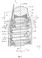
- FIG. 2 shows the sensor head 8 with the sensor head housing 14 FIG. 1 in a longitudinal section.
- the sensor head housing 14 forms a substantially rotationally symmetrical cavity 20 in which the electronic unit 22 is arranged.
- the electronics unit 22 is at least predominantly of an electronics housing 84 (see FIG. 3 ) enveloped, due to the selected cutting plane in FIG. 2 and a partial occlusion by the electronic unit 22 is not shown.
- the axis of rotation 24 of the sensor head housing 14 and the axis of rotation 26 of the electronics housing 84 are arranged coaxially.
- a sensor optic 32 comprising the optical element 16 or the optical lens 18, a filter 30 and a sensor 31 arranged on a circuit board 48, the optical element 16 being mounted in the sensor head housing 14.
- the optical element 16 may be mounted in the electronics housing 84.
- the optical element 16 or the optical lens 18 is arranged at an axial distance A1 to the filter 30, wherein the axial distance A1 is adjusted by an at least indirectly inserted between the optical lens 18 and the filter 30 Axialabstandsjustageelement 34.
- the Axialabstandsjustageelement 34 is in the present embodiment, a circular ring with a rectangular cross-section.
- the sensor 31 upstream filter 30 is in a circular holder 33 is supported, on the one hand the Axialabstandsjustageelement 34 at least partially rests and the other has a projection 33a with a rectangular cross-section, wherein the sensor 31 supporting board 48 and the holder 33 are at least partially connected to each other via the extension 33a.
- the holder 33 thus ensures a defined axial distance between the filter 30 and the sensor 31st
- the target value in the present exemplary embodiment is a value for setting the focus of the optical lens 18 on the sensor 31, which is located at a defined distance from the filter 30 via the holder 33.
- the deviation of the actual value of the distance A1 from the target value of the distance A1 results from manufacturing inaccuracies of the sensor head 8, in particular of the sensor head housing 14 and the electronics housing 84.
- the difference between the desired value and the actual value is determined by a measurement.
- the axial distance adjusting element 34 having a certain axial thickness A2 is selected from a set of axial distance adjusting elements having different axial thicknesses.
- a different axial distance adjusting element with an axial thickness deviating from A2 would accordingly be selected.
- the so selected Axialabstandsjustageelement 34 is mounted in the sensor head housing 14 and hereby the axial distance A1 between the lens 18 and the filter 30 and thus the axial distance A14 between the lens 18 and sensor 31 adjusted or adjusted the focus of the lens 18 on the sensor 31 ,
- the electronic unit 22 has seven boards 36, 38, 40, 42, 44, 46 and 48, which are arranged in seven planes 50, 52, 54, 56, 58, 60 and 62 in the axial direction 28 one above the other.
- the boards 36 to 48 are connected to six flexible flat cables 64, 66, 68, 70, 72 and 74. More specifically, each electrically conductive connects the first flat cable 64, the first board 36 to the second board 38, the second flat cable 66, the second board 38 to the third board 40, the third flat cable 68, the third board 40 to the fourth board 42, the fourth Flat cable 70, the fourth board 42 with the fifth board 44, the fifth flat cable 72, the fifth board 44 with the sixth board 46 and the sixth flat cable 74, the sixth board 46 with the seventh board 48.
- the flexible flat cables 64, 66, 68, 70, 72 and 74 are arranged meandering in the axial direction 28 meandering. Due to the resulting curvature, the flexible flat cables 64, 66, 68, 70, 72 and 74 each have a greater length than necessary for bridging the respective blank spacing.
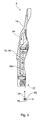
- FIG. 3 shows the sensor head 8 FIG. 1 in a sectional view with a relative to FIG. 2 rotated by 90 ° cutting plane, the representation is limited by a breaking edge on the features to be clarified here.
- the electronics unit 22 is enveloped at least predominantly by an electronics housing 84.
- the electronics housing 84 has a housing segment shell 86a. Between the electronics housing 84 and the sensor head housing 14, a thermal insulation layer 76 is disposed. In the present embodiment, this insulating layer 76 is formed by a radial air gap 80. In the area of the housing segment shell, the air gap 80 has a gap of approximately 0.5 mm. In the tangential direction 82, the insulation layer 76 or the air gap 80 extends approximately completely around the electronics housing 84. In the axial direction 28, the air gap 80 extends approximately over the entire axial length L (see FIG. 4 ) of the electronics housing 84.
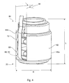
- FIG. 4 shows the electronics housing 84 from FIG. 3 with two housing segment shells 86a, 86b and arranged in the interior of the electronics housing 84 electronic unit 22 in a perspective view.
- the following descriptions are essentially limited to the differences from the previous embodiments, to which reference is made to the features and functions that remain the same. Substantially identical components are basically identified by the same reference numeral and features not mentioned are adopted in the following exemplary embodiments without being described again.
- the electronics housing 84 has a substantially rotationally symmetrical outer contour with a maximum diameter D and an axial length L and an opening 88 extending over approximately the entire axial length L.
- the electronics housing 84 encloses the electronics unit 22 predominantly, wherein in particular the flexible flat cables 66 and 70 of the electronics unit 22 are arranged in the opening 88.
- the opening 88 is designed as a gap 90 between the separate housing segment shells 86a and 86b, which each form a circular cylindrical outer surface 92 of the electronics housing 84.
- the gap has a tangential opening angle 94 of 60 °. Due to the perspective view in FIG. 3 is another identical by 180 ° to the gap 90 offset gap not visible. The gap 90 allows for ventilation of the electronics unit 22.
- the air gap 80 encloses the housing segment shells 86a, so that in the region of the housing segment shells 86a, 86b, a thermal bridge to the sensor head housing 14 is avoided.
- FIG. 5 shows the electronics housing 84 with the two housing segment shells 86a and 86b and the electronics unit 22 from FIG. 4 in a further sectional view.
- the electronics housing 84 on a support member 96 which supports a central region of the board 48 in the axial direction 28.
- the support member 96 is designed as a support wall 98 and arranged in the axial direction 28 between the two boards 46 and 48.
- the support wall is predominantly made of a metal, so that the board 46 is shielded from any electromagnetic radiation emanating from the board 48.
- the electronic unit 22 has an interface element 100.
- the interface element 100 is arranged on the circuit board 36 and projects beyond an edge 102 of the electronics housing 84 by a distance A3. Between the circuit board 36 - and thus at least indirectly between the interface element 100 and the electronics housing 22 - a further Axialabstandsjustageelement 104 is inserted.
- the Axialabstandsjustageelement 104 is executed in the present embodiment as a circular ring with a rectangular cross-section.
- a difference between a desired value and an actual value of the axial distance A3 between the interface element 100 and the edge 102 of the electronics housing 84 is determined.
- the desired value is a value for the production of a plug connection between the interface element 100 and an interface housing, not specified in detail, in accordance with requirements.
- the deviation of the actual value of the distance A3 from the target value of the distance A3 is due to manufacturing inaccuracies of the Sensor head 8, in particular of the electronics housing 84.
- the difference between the setpoint and the actual value is determined by a gauge.
- the axial distance adjusting element 104 having a certain axial thickness A4 is selected from a set of axial distance adjusting elements having different axial thicknesses.
- a different axial distance adjusting element with an axial thickness deviating from A4 would accordingly be selected.
- the so selected Axialabstandsjustageelement 104 is mounted in the electronics housing 84 and hereby the axial distance A3 between the interface element 100 and the edge 102 is adjusted.
- the housing segment shells 86 have a plurality of arcuate tangential grooves 106, 108, 110 and 112. The edge surfaces of the boards 38, 40, 42 and 44 are inserted into the tangential grooves 106, 108, 110 and 112.
- the boards 38, 40, 42 and 44 are inserted into the Tagentialnuten 106, 108, 110 and 112 and so fixed between the housing segment shells 86. More specifically, the peripheral edge 114a of the board 38 is inserted into the tangential groove 106a, the peripheral edge 116a of the board 40 into the tangential groove 108a, the peripheral edge 118a of the board 42 into the tangential groove 110a, and the peripheral edge 120a of the board 44 into the tangential groove 112a of the housing segment shell 86a , Thereafter, the GeHousegmentschale 86 b with the Tagentialnuten 106 b, 108 b, 110 b and 112 b mounted on the so partially fixed boards 38, 40, 42 and 44.
- the housing segment shell 86b with the tangential groove 106b is applied to the peripheral edge 114b of the board 38, the tangential groove 108b to the peripheral edge 116b of the board 40, the tangential groove 110b to the peripheral edge 118b of the board 42, and the tangential groove 112b to the peripheral edge 120b of the board 44 attached.
- the boards 38 to 44 are fixed between the housing segment shells 86 in the radial direction 78 and the axial direction 28.
- FIG. 6 shows a schematic representation of a system 122 of a plurality of sensor heads 8, wherein representation is limited for reasons of clarity on only two sensor heads 8a and 8b.
- the optical lens 18a is disposed at an axial distance A5 from the filter 30a, the axial distance A5 being adjusted by the axial distance adjusting member 34a.
- its optical lens 18b to the filter 30b is likewise arranged at the axial distance A5.
- the axial distance A5 is adjusted at the sensor head 8b by the axial distance adjusting member 34b.
- the interface element 100a is disposed at an axial distance A9 to the edge 102a, the axial distance A9 being adjusted by the axial distance adjusting element 104a.
- its interface element 100b to the edge 102b is likewise arranged at the axial distance A9.
- the axial distance A9 is adjusted at the sensor head 8b by the axial distance adjusting element 104b.
- the distance from the rear edge 103 of the sensor head housing 14 to the interface element 100 is adjusted to allow a realization of a plug connection between the interface element 100 and an interface housing, not shown. For this purpose, it is necessary for the interface element 100 to project beyond the rear edge 103 of the sensor head housing 14 by the distance A16.
Landscapes
- Engineering & Computer Science (AREA)
- Microelectronics & Electronic Packaging (AREA)
- Chemical & Material Sciences (AREA)
- Combustion & Propulsion (AREA)
- General Engineering & Computer Science (AREA)
- Physics & Mathematics (AREA)
- Electromagnetism (AREA)
- Thermal Sciences (AREA)
- Switches Operated By Changes In Physical Conditions (AREA)
- Measurement Of Length, Angles, Or The Like Using Electric Or Magnetic Means (AREA)
Abstract
Description
- Die Erfindung betrifft einen Sensorkopf für einen Flugkörper, mit einem Sensorkopfgehäuse, einer Elektronikeinheit und einem Elektronikgehäuse um die Elektronikeinheit.
- Flugkörper weisen im Bugbereich ihres Rumpfes häufig einen Sensorkopf zur Messgrößenerfassung auf. Diese Messgrößenerfassung erfolgt üblicherweise durch eine im Sensorkopf angeordnete Elektronikeinheit und dient der Zielführung des Flugkörpers. Eine solche Elektronikeinheit umfasst üblicherweise eine Anzahl von Platinen, die jeweils mit einer Anzahl von elektronischen Komponenten bestückt sind.
- Je nach Flugkörpertyp und Flugbedingungen kann der Sensorkopf extremen Beschleunigungen und hohen Geschwindigkeiten ausgesetzt sein. Dies ist insbesondere bei Präzisionsmunition, wie beispielsweise einem zielgeführten Artilleriegeschoss, der Fall. Die dort auftretenden Beschleunigungen können beim Abschuss bis zu 26.000 g betragen. Um eine stets präzise Zielführung des Flugkörpers zu gewährleisten, ist eine verlässliche Funktion der Elektronikeinheit auch unter solch extremen Bedingungen notwendig.
- Aus der
WO 2011/014287 A2 ist eine Elektronikeinheit für einen Flugkörper bekannt. Die Elektronikeinheit weist unter anderem ein Elektronikgehäuse mit einer Kavität und zwei übereinander angeordnete, durch sog. Stützstrukturen getragene Platinen auf. Das Gehäuse ist dazu vorbereitet in ein Sensorkopfgehäuse eingepasst zu werden. Zu diesem Zweck weist das Elektronikgehäuse eine der Innenkontur des Sensorkopfgehäuses entsprechende Außenkontur auf. - Es ist eine Aufgabe der vorliegenden Erfindung, einen robusten Sensorkopf anzugeben.
- Diese Aufgabe wird durch einen Sensorkopf der eingangs genannten Art gelöst, bei dem erfindungsgemäß das Elektronikgehäuse die Elektronikeinheit zumindest überwiegend umhüllt und eine im Wesentlichen rotationssymmetrische Außenkontur aufweist und in einem durch das Sensorkopfgehäuse gebildeten im Wesentlichen rotationssymmetrischen Hohlraum rotationsachsenparallel angeordnet ist, wobei eine thermische Isolationsschicht zwischen dem Elektronikgehäuse und dem Sensorkopfgehäuse angeordnet ist.
- Die Erfindung geht dabei von der Überlegung aus, dass Flugkörper, beispielsweise langreichweitig verschossene Rohrmunition, über große Distanzen mit hohen Geschwindigkeiten durch die Atmosphäre fliegen. Hierbei können luftreibungsbedingte Temperaturen von 250° C und darüber am Flugkörperbug auftreten. Die maximal zulässige Temperatur von Elektronikbauteilen der Elektronikeinheit liegt hingegen üblicherweise bei lediglich 100° C. Die Funktion der Elektronikeinheit - und damit beispielsweise die präzise Zielführung des Flugkörpers - kann durch die Reibungswärme während eines Fluges des Flugkörpers mit hoher Geschwindigkeit beeinträchtigt werden. Dies kann insbesondere der Fall sein, wenn der Sensorkopf zwischen dem Gehäuse der Elektronikeinheit und dem Gehäuse des Sensorkopfes eine vergleichsweise große Kontaktfläche als Wärmebrücke aufweist. Hierdurch wird die Wärmeleitung zwischen beiden Gehäusen begünstigt, sodass die Reibungswärme bis zur Elektronikeinheit vordringen, diese unzulässig stark erwärmen und folglich bis hin zum Funktionsausfall beeinträchtigen kann. Durch die Anordnung einer thermischen Isolationsschicht zwischen dem Sensorkopfgehäuse und dem Elektronikgehäuse kann diese Wärmeleitung vermindert, so die Erwärmung der Elektronikeinheit durch die Reibungswärme reduziert und folglich ein Ausfall der Elektronikeinheit durch Überhitzen vermieden werden.
- Die Erfindung ist besonders vorteilhaft anwendbar bei einem Flugkörper, ausgeführt als Präzisionsmunition, insbesondere ausgeführt als gelenktes Artilleriegeschoss. Bei diesem Flugkörpertyp ist die auftretende Reibungswärme aufgrund der hohen Fluggeschwindigkeit von bis zu 1 km/s besonders hoch, sodass die thermische Isolationsschicht besonders wirksam ein Versagensrisiko der Elektronikeinheit infolge eines Überhitzens vermindern kann.
- Das Sensorkopfgehäuse kann zur Montage am Rumpf eines Flugkörpers vorbereitet sein oder dazu geeignet sein, den Rumpfbug eines Flugkörpers zu bilden. Der durch das Sensorkopfgehäuse gebildete im Wesentlichen rotationssymmetrische Hohlraum kann eine Röhren-, Zylinder- und/oder Konusform aufweisen.
- Die Elektronikeinheit umfasst zumindest eine Platine bzw. eine Leiterplatte mit einer Mehrzahl von Elektronikkomponenten, insbesondere optoelektronische Komponenten. Die Elektronikeinheit ist zum zumindest überwiegenden Vollbringen einer Funktion, beispielsweise einer optoelektronischen Zielerfassungsfunktion zur Zielführung des Flugkörpers, vorbereitet.
- Das Elektronikgehäuse ist insbesondere koaxial im Sensorkopfgehäuse angeordnet, sodass eine drallbedingte Unwucht während eines Fluges des Flugkörpers vermindert wird. Die im Wesentlichen rotationssymmetrische Außenkontur des Elektronikgehäuses kann im Wesentlichen eine Röhren-, Zylinder- und/oder Konusform aufweisen.
- Die thermische Isolationsschicht ist insbesondere radial zwischen dem Elektronikgehäuse und dem Sensorkopfgehäuse angeordnet. Die thermische Isolationsschicht kann in einem Spalt zwischen dem Elektronikgehäuse und dem Sensorkopfgehäuse angeordnet oder durch diesen gebildet sein.
- In einer vorteilhaften Ausführungsform der Erfindung ist die Isolationsschicht durch einen radialen Luftspalt zwischen dem Elektronikgehäuse und dem Sensorkopfgehäuse von zumindest 1 %, vorzugsweise zumindest 2 %, des maximalen Durchmessers des Elektronikgehäuses gebildet. Das Luftspaltmaß kann durch eine entsprechende Dimensionierung des Außendurchmessers des Elektronikgehäuses und des Innendurchmessers des Sensorkopfgehäuses mit einfachen Mitteln mit einem vorgegebenen Wert realisiert werden. Der radiale Luftspalt weist ein zum Zweck der wirksamen thermischen Isolation ermitteltes Maß auf. Der Luftspalt unterscheidet sich technisch wesentlich von einem toleranzbedingten, ungewollten Spiel zwischen dem Elektronikgehäuse und dem Sensorkopfgehäuse, das bei Flugkörpern, insbesondere abschussfesten Flugkörpern, 50 µm nicht übersteigen sollte. Um eine gute thermische Isolierung zu gewährleisten, ist ein Spaltmaß von zumindest 0,2 mm, insbesondere von zumindest 0,5 mm, vorteilhaft.
- Anstelle eines vollständig mit Gas gefüllten Spalts kann ein festes, plastisches oder gießbares Isolationsmaterial zumindest einen Teil der Isolationsschicht bilden. Ein die thermische Isolationsschicht bildendes Material kann zum Eingießen in den Spalt und insbesondere zum zumindest überwiegenden Ausfüllen des Spalts vorbereitet sein. Vorteilhafterweise erstreckt sich die Isolationsschicht in tangentialer Richtung umlaufend über zumindest 270°, vorzugsweise über mehr als 330°, um das Elektronikgehäuse. Durch die derartige Ummantelung des Elektronikgehäuses mit der Isolationsschicht wird einer Bildung von Wärmebrücken zwischen dem Elektronik- und dem Sensorkopfgehäuse entgegengewirkt. Die Isolationsschicht kann sich in tangentialer Richtung abschnittsweise, also aus mehreren separaten Isolationsschichtabschnitten bestehend, um das Elektronikgehäuse erstrecken.
- Zweckmäßigerweise erstreckt sich die Isolationsschicht in axialer Richtung über zumindest die Hälfte, insbesondere zumindest 80 % der axialen Länge des Elektronikgehäuses. Die Isolationsschicht kann sich in axialer Richtung abschnittsweise, also aus mehreren separaten Isolationsschichtabschnitten bestehend, über das Elektronikgehäuse erstrecken. Eine verbleibende Wärmebrücke zwischen Sensorkopf- und Elektronikgehäuse ist zweckmäßigerweise in einem Bereich angeordnet, innerhalb dessen keine oder nur einzelne, temperaturbeständige Elektronikbauelemente angeordnet sind.
- Eine besonders wirksame thermische Isolation der Elektronikeinheit kann erreicht werden, wenn die Isolationsschicht einen zumindest überwiegenden Anteil, insbesondere mehr als 80 %, der Außenfläche des Elektronikgehäuses ummantelt. Dies kann besonders einfach erreicht werden, wenn das Elektronikgehäuse zumindest überwiegend an einer seiner Stirnseiten in dem Sensorkopfgehäuse befestigt wird, sodass die verbleibende Außenfläche des Elektronikgehäuses zumindest überwiegend kontaktfrei zur Innenfläche des Sensorkopfgehäuses angeordnet ist. Beispielsweise ist das Elektronikgehäuse an seiner bugseitigen Stirnseite in eine Fassung im Sensorkopfgehäuse eingesteckt, wobei die Außenfläche des Elektronikgehäuses in einem vorgegebenen Abstand zur Innenfläche des Sensorkopfgehäuses radial fixiert ist.
- In einer vorteilhaften Ausführungsform weist das Elektronikgehäuse eine über zumindest einen überwiegenden Anteil der axialen Länge des Elektronikgehäuses verlaufende Öffnung auf. Diese Öffnung kann als ein Schlitz, eine Aussparung, eine Auslassung oder ein Spalt ausgeführt sein. Die Öffnung bewirkt, dass die Elektronikeinheit teilweise nicht von dem Elektronikgehäuse umschlossen ist, sodass die Elektronikeinheit zumindest teilweise an die Isolationsschicht angrenzen kann. Die Öffnung kann so ausgeführt sein, dass sich die Isolationsschicht in das Innere des Elektronikgehäuses erstreckt. Insbesondere, wenn die Isolationsschicht als Luftspalt ausgeführt ist, entsteht durch die Öffnung im Bereich der Öffnung ein radial vertiefter Luftspalt, sodass Konvektion und/oder eine verbesserte Isolationswirkung erzielt werden kann. Vorteilhafterweise kann das Elektronikgehäuse mehrere, insbesondere zwei, solcher Öffnungen aufweisen.
- Zweckmäßigerweise ist die Öffnung eine Lücke zwischen zwei separaten Gehäusesegmentschalen. Die Öffnung kann auf diese Weise aufwandsgünstig hergestellt werden, da auf zusätzliche Fertigungsschritte zum Einbringen der Öffnung, beispielsweise durch eine spanende Bearbeitung des Elektronikgehäuses, verzichtet werden kann. Vorteilhafterweise sind mehrere Lücken in regelmäßigen Abständen über den Umfang des Elektronikgehäuses vorgesehen. So kann eine Umwucht des Flugkörpers bei einem Rollen vermieden werden, insbesondere bei drallbehafteten Geschossen, die mit bis zu 150 U/s um ihre Längsachse rotieren.
- Vorteilhafterweise weist die Lücke einen tangentialen Öffnungswinkel von zumindest 30°, vorzugsweise 60°, auf. Auf diese Weise wird eine vergleichsweise große Öffnung erreicht, sodass die Isolationsschicht, also insbesondere der Luftspalt, die Komponenten der Elektronikeinheit besser erreichen kann. Insbesondere, wenn die Elektronikeinheit mehrere in axialer Richtung übereinander beabstandet angeordnete Platinen aufweist, kann so erreicht werden, dass die Luft des Luftspalts zwischen den Platinen zirkulieren kann. Durch dieses Zirkulieren des Luftspalts kann ein konvektionsbedingter Kühleffekt erzielt werden, wodurch einer Überhitzung der Elektronikeinheit entgegengewirkt werden kann.
- In einer vorteilhaften Weiterbildung weist das Elektronikgehäuse zumindest eine Gehäusesegmentschale mit einer innenliegend ausgebildeten kreisbogenförmigen Tangentialnut und einer kreiszylindrischen Außenfläche auf. In die Tangentialnut kann eine Platine oder generell ein Elektronikträger eingeführt sein, der im Folgenden der Einfachheit halber auch als Platine bezeichnet wird.
- Die Außenfläche der Gehäusesegmentschale kann im Wesentlichen zylindrisch sein und sich tangential über zumindest 90°, vorzugsweise 120° erstrecken. Zweckmäßigerweise bilden mindestens zwei Gehäusesegmentschalen das Elektronikgehäuse zumindest teilweise. Die Gehäusesegmentschalen können an gegenüberliegenden Seiten der Elektronikeinheit angeordnet sein und diese backenartig umfassen. Vorteilhafterweise sind mehrere Gehäusesegmentschalen in regelmäßigen Abständen über den Umfang der Elektronikeinheit angeordnet. So kann eine Umwucht des Flugkörpers bei einem Rollen während des Fluges vermieden werden.
- Die Erfindung ist außerdem gerichtet auf einen Sensorkopf der eingangs genannten Art, bei dem die Elektronikeinheit erfindungsgemäß in zumindest drei parallelen Ebenen - axial übereinander angeordnet - eine erste, eine zweite und zumindest eine dritte Platine umfasst, ein erstes flexibles Flachkabel die erste mit der zweiten Platine elektrisch leitfähig verbindet, ein zweites flexibles Flachkabel die zweite mit der dritten Platine elektrisch leitfähig verbindet und die beiden flexiblen Flachkabel in axialer Richtung mäanderförmig die Platinen verbindend angeordnet sind.
- Eine mäanderförmige Anordnung kann erreicht werden, wenn das erste und das zweite flexible Flachkabel an gegenüberliegenden Kanten der zweiten Platinen angeordnet. sind und insbesondere bogenförmig gekrümmt in entgegengesetzte Richtungen weisen. Durch die Krümmung weisen die flexiblen Flachkabel eine größer als zur Überbrückung des Platinenabstands notwendige Länge auf. Durch diese mäanderförmige Kabelverbindung kann erreicht werden, dass die Platinen der Elektronikeinheit, sofern sie noch nicht fest in dem Elektronikgehäuse montiert sind, in hohem Maße axial zueinander beweglich sind. Insbesondere kann so eine ziehharmonikaartige Bewegung der Platinen erreicht werden, wobei einem ungewollten Lösen der elektrisch leitfähigen Verbindung durch die flexible, mäanderförmige Verbindung entgegengewirkt wird. Die Montage der Elektronikeinheit im Elektronikgehäuse kann deshalb aufwandsgünstig realisiert werden. Eine präzise und damit in der Regel aufwändige Fertigung des Elektronikgehäuses, insbesondere der zur Aufnahme der Platinen vorbereiteten Tangentialnuten, kann ebenso vermieden werden, da diese Art der Flachkabelanordnung Abstandstoleranzen ausgleichen kann.
- Die Erfindung ist außerdem gerichtet auf einen Sensorkopf der eingangs genannten Art, der erfindungsgemäß eine Sensoroptik mit zumindest einem optischen Element und einen in einem axialen Abstand zum optischen Element angeordneten Sensor aufweist, wobei der axiale Abstand durch ein zumindest mittelbar zwischen dem optischen Element und dem Sensor eingefügtes Axialabstandsjustageelement justiert ist.
- Die Sensoroptik kann zur optischen Erfassung von Zielen des Flugkörpers vorbereitet sein. Das optische Element der Sensoroptik ist insbesondere eine optische Linse bzw. ein Objektiv. Das optische Element kann in einem Optiklager, das beispielsweise zur Aufnahme und Fassung einer Linse vorbereitet ist, gelagert sein. Das optische Element kann ein Teil der Elektronikeinheit sein.
- Der Sensor kann ein optoelektronischer Detektor sein. Zweckmäßigerweise kann der Sensor ein Teil der Elektronikeinheit, insbesondere eine auf einer Platine der Elektronikeinheit montierte elektronische Komponente, sein. Der Sensor kann in einem Sensorlager gelagert sein.
- Der axiale Abstand zwischen dem optischen Element und dem Sensor kann ein bestimmter Abstand sein, der erforderlich ist, um eine Funktion des Sensorkopfes, insbesondere eine optoelektronische Zielerfassung, zu erreichen.
- Das Axialabstandsjustageelement kann zwischen dem optischen Element und dem Sensor in den Sensorkopf eingelegt sein, so dass der Abstand zwischen dem optischen Element und dem Sensor durch das Axialabstandsjustageelement justiert, also eingestellt, ist. Das Axialabstandsjustageelement kann ein Ring, eine gelochte Scheibe, eine Platte mit einer Öffnung oder dergleichen sein. Beispielsweise ist das Axialabstandsjustageelement zwischen dem Sensorlager und dem Optiklager in den Sensorkopf eingefügt.
- Durch das Axialabstandsjustageelement kann ein von dem bestimmten Abstand abweichender Abstand zwischen dem optischen Element und dem Sensor mit einfachen Mitteln ausgeglichen werden. Eine präzise und in der Regel aufwändige Fertigung des Sensorkopfs, insbesondere hinsichtlich des Abstandsmaßes zwischen dem optischen Element und dem Sensor, kann deshalb vermieden werden.
- Zweckmäßigerweise ist das optische Element im Sensorkopfgehäuse gelagert. Das Sensorkopfgehäuse kann zu diesem Zweck eine entsprechende Fassung oder Halterung für eine optische Linse aufweisen.
- In einer anderen Ausführungsvariante ist das optische Element im Elektronikgehäuse gelagert. Das Elektronikgehäuse kann hierfür eine Fassung oder eine Halterung aufweisen, in der das optische Element angeordnet ist.
- Des Weiteren ist die Erfindung gerichtet auf einen Sensorkopf der eingangs genannten Art. Der Sensorkopf sieht erfindungsgemäß ein in einem axialen Abstand zu einer Kante des Elektronikgehäuses angeordnetes Schnittstellenelement vor, wobei der axiale Abstand durch ein zumindest mittelbar zwischen dem Schnittstellenelement und dem Elektronikgehäuse eingefügtes Axialabstandsjustageelement justiert ist.
- Die Kante des Elektronikgehäuses ist zweckmäßigerweise eine das hintere Ende des Elektronikgehäuses bildende Kante. Das Schnittstellenelement ist beispielsweise ein Stecker, der zur Herstellung einer Steckverbindung mit einer Steckerkupplung vorbereitet ist. Außerdem kann das Schnittstellenelement zur Leitung von elektrischen Signalen vorbereitet sein, die zur Zielführung des Flugkörpers dienen. Um eine zuverlässige Herstellbarkeit der Steckverbindung zu erreichen, ist es notwendig, dass das Schnittstellenelement in einem bestimmten axialen Abstand zu der Kante des Elektronikgehäuses angeordnet ist- bzw. dass das Schnittstellenelement um einen bestimmten axialen Abstand über die heckseitige Kante des Sensorkopfgehäuses herausragt.
- Das Axialabstandsjustageelement kann ein Ring, eine gelochte Scheibe oder eine Platte mit einer Öffnung sein. Beispielsweise ist das Axialabstandsjustageelement zwischen einer das Schnittstellenelement tragenden Platine und einer Wand des Elektronikgehäuses eingefügt.
- Auf diese Weise kann eine präzise und in der Regel aufwändige Fertigung des Sensorkopfs, insbesondere hinsichtlich des Abstandsmaßes zwischen dem Schnittstellenelement und der Kante des Elektronikgehäuses, vermieden werden.
- Zudem ist die Erfindung gerichtet auf ein System aus mehreren erfindungsgemäßen Sensorköpfen, wobei die jeweils an der gleichen Stelle angeordneten Axialabstandsjustageelemente der Sensorköpfe eine Axialdickendifferenz von zumindest 0,2 mm, vorzugsweise zumindest 0,7 mm, aufweisen. Jeder der Sensorköpfe des Systems weist zumindest ein Axialabstandsjustageelement auf. Die Axialabstandsjustageelemente des Systems sind jeweils an der gleichen Stelle angeordnet, also beispielsweise zwischen dem optischen Element und dem Sensor. Die Axialdickendifferenz ergibt sich aus dem Zweck der Abstandsjustage, die in der Regel für jeden Sensorkopf des Systems eine verschiedene Axialdicke des Axialabstandsjustageelements erfordert. In der Erprobung hat sich gezeigt, dass eine Axialdickendifferenz von zumindest 0,2 mm, vorzugsweise von 0,7 mm, zur zweckmäßigen Axialabstandsjustage für eine Vielzahl von Sensorköpfen ausreichend ist. In einigen Fällen kann es vorteilhaft sein, eine Axialdickendifferenz von mehr als 1 mm, beispielsweise 2 mm, vorzusehen.
- Eine weitere vorteilhafte Ausführungsform sieht ein im Elektronikgehäuse abgestütztes Stützelement vor, das einen mittleren Bereich einer Platine der Elektronikeinheit in axialer Richtung hinterstützend angeordnet ist. Das Stützelement kann eine Verstrebung, eine Platte oder ein Balken sein, die bzw. der in dem Elektronikgehäuse befestigt ist. Die Platine liegt zumindest teilweise mit ihrem mittleren Bereich auf dem Stützelement auf. Die Platine kann eine Kreisscheibe sein. Durch das so angeordnete Abstützelement wird eine übermäßige Deformation der Platine durch die Einwirkung von Trägheitskräften während des Starts des Flugkörpers vermieden. Dies ist insbesondere bei einem als gelenktes Artilleriegeschoss ausgeführten Flugkörper von Vorteil, da die dort auftretende Abschussbeschleunigung bis zu 26.000 g erreichen kann, was ohne eine entsprechende Vorkehrung zu einer starken Deformation und/oder dem Versagen der Platine der Elektronikeinheit führen kann.
- Weiterhin ist es vorteilhaft, wenn das Stützelement eine Stützwand ist und in axialer Richtung zwischen zwei Platinen der Elektronikeinheit angeordnet ist und zumindest überwiegend aus Metall besteht. Durch die Anordnung zwischen den beiden Platinen und den metallischen Werkstoff kann auf einfache Weise eine elektromagnetische Abschirmung zumindest einer der Platinen von einer elektromagnetischen Einwirkung durch die andere der beiden Platinen erfolgen. Durch die Doppelfunktion der Stützwand, nämlich der Abstützung bei einem Start und der Abschirmung gegen Strahlung, können diese Funktionen besonders aufwandsgünstig mit einem Mittel - nämlich der Stützwand - erreicht werden.
- Zudem ist die Erfindung auf ein Verfahren zur Montage eines Sensorkopfs gerichtet.
- Das Verfahren sieht vor, dass erfindungsgemäß eine Differenz zwischen einem Sollwert und einem Istwert eines axialen Abstands zwischen zwei Elementen des Sensorkopfs ermittelt wird. Der Sollwert kann ein Wert eines axialen Abstands zu einer Einstellung, insbesondere einer Scharfstellung, des Fokus der Linse auf dem Sensor sein. Hierfür können die Elemente eine Linse und ein Sensor sein. Eine Abweichung des Istwerts des Abstands vom Sollwert des Abstands kann sich aus einer zwangsläufig unvollkommenen Fertigung ergeben. Die Differenz zwischen dem Sollwert und dem Istwert kann durch eine Messung oder mit einer Maßlehre ermittelt werden.
- Unter Verwendung des ermittelten Abstandswerts wird ein Axialabstandsjustageelement mit einer bestimmten Axialdicke aus einem Satz von Axialabstandsjustageelementen mit unterschiedlichen Axialdicken ausgewählt. Der Satz von Axialabstandsjustageelementen kann eine Vielzahl von Elementen umfassen, deren Axialdicken sich bis zu 0,2 mm, insbesondere um bis zu 2 mm, voneinander unterscheiden können.
- Das so ausgewählte Axialabstandsjustageelement wird im Sensorkopf montiert und hiermit der axiale Abstand zwischen der Linse und dem Sensor justiert. Auf diese Weise kann der erforderliche Abstand unter Vermeidung einer aufwändigen präzisen Fertigung bzw. eines aufwändigen Nacharbeitens an dem Sensorkopf aufwandsgünstig erreicht werden.
- Es ist ebenfalls möglich, dass die beiden Elemente ein Schnittstellenelement und eine Kante eines Elektronikgehäuses des Sensorkopfs sind. Der Sollwert kann ein zu einer Herstellbarkeit einer Schnittstellenverbindung, insbesondere einer Steckverbindung, erforderlicher Wert sein. Der Istwert des Abstands ergibt sich aus der zwangsläufig unvollkommenen Fertigung bzw. aus Toleranzen des Schnittstellenelements. Die Differenz zwischen dem Sollwert und dem Istwert kann durch eine Messung oder mit einer Maßlehre ermittelt werden.
- Das so ausgewählte Axialabstandsjustageelement wird im Sensorkopf montiert und hiermit der axiale Abstand zwischen dem Schnittstellenelement und der Kante des Elektronikgehäuses justiert. Auf diese Weise kann dieser erforderliche Abstand unter Vermeidung einer aufwändigen präzisen Fertigung bzw. eines aufwändigen Nacharbeitens an dem Sensorkopf aufwandsgünstig erreicht werden.
- Des Weiteren ist die Erfindung gerichtet auf ein Verfahren zur Montage eines Sensorkopfs, bei dem ein Anteil einer Umfangskante einer Platine einer Elektronikeinheit in eine Nut einer Gehäusesegmentschale eines Elektronikgehäuses eingesteckt wird. Die Umfangskante der Platine kann kreisbogenförmig, insbesondere kreisförmig sein. Die Nut kann kreisbogenförmig sein. Insbesondere kann die Nut in Dickenrichtung so bemessen sein, dass eine kraftschlüssige Steckverbindung zwischen der Gehäusesegmentschale und der Platine erreicht wird. Die Gehäusesegmentschale kann mehrere Nuten zur Aufnahme mehrerer Platinen aufweisen. Es kann möglich sein, mehr als eine Platine in eine Nut einzustecken.
- Eine mit einer weiteren Nut versehene weitere Gehäusesegmentschale wird mit dieser weiteren Nut auf einen weiteren Anteil der Umfangskante der Platine aufgesteckt. Zweckmäßigerweise wird die Gehäusesegmentschale auf die der ersten Gehäusesegmentschale gegenüberliegende Umfangskante bzw. bei einer umlaufenden Umfangskante auf die gegenüberliegende Seite, aufgesteckt, sodass die Platine backenartig durch die beiden Gehäusesegmentschalen umgriffen wird.
- Die Platine wird von den Gehäusesegmentschalen in radialer Richtung zwischen diesen fixiert und hiermit zumindest ein Teil der Elektronikeinheit - nämlich die Platine - in dem Elektronikgehäuse montiert. Durch die beschriebene Steckverbindung zwischen mehreren, insbesondere zwei, Gehäusesegmentschalen, ist die Elektronikeinheit besonders einfach in dem Elektronikgehäuse montierbar. Ferner sind die Platine bzw. deren elektronische Komponenten durch ein bloßes Entfernen einer der Gehäusesegmentschalen gut erreichbar, was beispielsweise zum Entfernen und Ersetzen einer elektronischen Komponente vorteilhaft sein kann.
- Die bisher gegebene Beschreibung vorteilhafter Ausgestaltungen der Erfindung enthält zahlreiche Merkmale, die in den einzelnen Unteransprüchen teilweise zu mehreren zusammengefasst wiedergegeben sind. Diese Merkmale können jedoch zweckmäßigerweise auch einzeln betrachtet und zu sinnvollen weiteren Kombinationen zusammenfasst werden. Insbesondere sind diese Merkmale jeweils einzeln und in beliebiger geeigneter Kombination mit dem erfindungsgemäßen Verfahren und der erfindungsgemäßen Vorrichtung gemäß den unabhängigen Ansprüchen kombinierbar.
- Die oben beschriebenen Eigenschaften, Merkmale und Vorteile dieser Erfindung, sowie die Art und Weise, wie diese erreicht werden, werden klarer und deutlicher verständlich im Zusammenhang mit der folgenden Beschreibung der Ausführungsbeispiele, die im Zusammenhang mit den Zeichnungen näher erläutert werden. Die Ausführungsbeispiele dienen der Erläuterung der Erfindung und beschränken die Erfindung nicht auf die darin angegebene Kombination von Merkmalen, auch nicht in Bezug auf funktionale Merkmale. Außerdem können dazu geeignete Merkmale eines jeden Ausführungsbeispiels auch explizit isoliert betrachtet, aus einem Ausführungsbeispiel entfernt, in ein anderes Ausführungsbeispiel zu dessen Ergänzung eingebracht und/oder mit einem beliebigen der Ansprüche kombiniert werden.
- Es zeigen:
- FIG 1
- einen Flugkörper mit einem Sensorkopf mit einem Sensorkopfgehäuse und einer Bughaube,
- FIG 2
- den Sensorkopf aus
FIG 1 mit einer im Inneren des Sensorkopfgehäuses montierter Elektronikeinheit in einer Schnittdarstellung, - FIG 3
- den Sensorkopf aus
FIG 1 in einer Schnittdarstellung mit einer relativ zuFIG 2 um 90° gedrehten Schnittebene, - FIG 4
- ein Elektronikgehäuse mit Gehäusesegmentschalen und der Elektronikeinheit aus
FIG 2 , - FIG 5
- das Elektronikgehäuse und die Elektronikeinheit aus
FIG 4 in einer Schnittdarstellung und - FIG 6
- ein System aus mehreren Sensorköpfen.
-
FIG 1 zeigt eine schematische Darstellung eines Flugkörpers 2 mit einem Rumpf 4 mit heckseitig ausgebildeten Tragflügeln 6, einem Sensorkopf 8 und einer Bughaube 10. Die Bughaube 10 ist in einem Längsschnitt dargestellt und bildet den in einer Flugrichtung 12 vordersten Teil des Flugkörpers 2. Der Sensorkopf 8 weist ein rotationssymmetrisches Sensorkopfgehäuse 14 und ein optisches Element 16 auf, das im vorliegenden Ausführungsbeispiel als optische Linse 18 ausgeführt ist. Der Sensorkopf 8 ist zur Erfassung von Zielen und/oder zur Zielführung des Flugkörpers 2 mittels des optischen Elements 16 und einer im Inneren des Sensorkopfgehäuses 14 montierten Elektronikeinheit 22 (sieheFIG 2 ) vorbereitet. Die Bughaube 10 ist auf das Sensorkopfgehäuse 14 aufgesteckt und deckt insbesondere das optische Element 16 bzw. die optische Linse 18 zum Schutz vor Beschädigungen ab. - Im vorliegenden Ausführungsbeispiel ist der Flugkörper 2 als gelenktes Artilleriegeschoss ausgeführt, sodass die Fluggeschwindigkeit des Flugkörpers 2 bis zu 1 km/s beträgt. Durch die dabei auftretende Luftreibung treten hohe Temperaturen von bis zu 300° C an der Außenfläche des Flugkörpers 2, insbesondere am vordersten Bereich des Flugkörpers 2 bzw. dessen Bug, auf.
- Nach einem Start des Flugkörpers 2 und in einer frühen Flugphase ist die Bughaube 10 in der Regel das durch die Luftreibung thermisch am höchsten beanspruchte Bauteil des Flugkörpers 2.
- Die Bughaube 10 ist zum Abwerfen zu einem vorgegebenen Zeitpunkt während eines Fluges des Flugkörpers 2 vorbereitet, sodass der Sensorkopf 8 nach diesem vorgegebenen Zeitpunkt bis zum Eintreffen des Flugkörpers 2 in einem Ziel den vordersten Bereich des Flugkörpers 2 bildet. Infolgedessen wird das Sensorkopfgehäuse 14 ab diesem vorgegebenen Zeitpunkt durch die einwirkende Reibungswärme thermisch hoch beansprucht. Die Reibungswärme wird durch die Wärmeleitung teilweise bis in das Innere des Sensorkopfgehäuses 14 transportiert und führt so zu einer Erwärmung der in dessen Inneren montierten Komponenten. Um eine unzulässig hohe thermische Beanspruchung der im Inneren des Sensorkopfgehäuses 14 angeordneten Elektronikeinheit 22 - und damit einen möglichen Ausfall der Zielführungsfunktion des Flugkörpers 2 - zu vermeiden, müssen entsprechende technische Vorkehrungen getroffen werden.
-
FIG 2 zeigt den Sensorkopf 8 mit dem Sensorkopfgehäuse 14 ausFIG 1 in einem Längsschnitt. Das Sensorkopfgehäuse 14 bildet einen im Wesentlichen rotationssymmetrischen Hohlraum 20 in dem die Elektronikeinheit 22 angeordnet ist. Die Elektronikeinheit 22 wird zumindest überwiegend von einem Elektronikgehäuse 84 (sieheFIG 3 ) umhüllt, das aufgrund der gewählten Schnittebene inFIG 2 und einer teilweisen Verdeckung durch die Elektronikeinheit 22 nicht dargestellt ist. Die Rotationsachse 24 des Sensorkopfgehäuses 14 und die Rotationsachse 26 des Elektronikgehäuses 84 sind koaxial angeordnet. - In axialer Richtung 28 oberhalb der Elektronikeinheit 22 ist eine das optische Element 16 bzw. die optische Linse 18, einen Filter 30 und einen auf einer Platine 48 angeordneten Sensor 31 umfassende Sensoroptik 32 angeordnet, wobei das optische Element 16 im Sensorkopfgehäuse 14 gelagert ist. In einem anderen vorliegend nicht näher beschriebenen Ausführungsbeispiel kann das optische Element 16 im Elektronikgehäuse 84 gelagert sein. Das optische Element 16 bzw. die optische Linse 18 ist in einem axialen Abstand A1 zum Filter 30 angeordnet, wobei der axiale Abstand A1 durch ein zumindest mittelbar zwischen der optischen Linse 18 und dem Filter 30 eingefügtes Axialabstandsjustageelement 34 justiert ist. Das Axialabstandsjustageelement 34 ist im vorliegenden Ausführungsbeispiel ein Kreisring mit einem rechteckigen Querschnitt. Der dem Sensor 31 vorgeordnete Filter 30 ist in einer kreisförmigen Halterung 33 gehaltert, auf der zum einen das Axialabstandsjustageelement 34 zumindest teilweise aufliegt und die zum anderen einen Fortsatz 33a mit rechteckförmigem Querschnitt aufweist, wobei die den Sensor 31 tragende Platine 48 und die Halterung 33 über den Fortsatz 33a zumindest bereichsweise miteinander verbunden sind. Die Halterung 33 sorgt somit für einen definierten axialen Abstand zwischen Filter 30 und Sensor 31.
- Zur Montage des Sensorkopfs 8 wird eine Differenz zwischen einem Sollwert und einem Istwert des axialen Abstands A1 zwischen der optischen Linse 18 und dem Filter 30 ermittelt. Der Sollwert ist im vorliegenden Ausführungsbeispiel ein Wert zu einer Einstellung des Fokus der optischen Linse 18 auf dem Sensor 31, welcher sich über die Halterung 33 in einem definierten Abstand zum Filter 30 befindet. Die Abweichung des Istwerts des Abstands A1 vom Sollwert des Abstands A1 ergibt sich infolge von Fertigungsungenauigkeiten des Sensorkopfs 8, insbesondere des Sensorkopfgehäuses 14 und des Elektronikgehäuses 84. Die Differenz zwischen dem Sollwert und dem Istwert wird durch eine Messung ermittelt.
- Unter Verwendung des so ermittelten Abstandswerts wird das Axialabstandsjustageelement 34 mit einer bestimmten Axialdicke A2 aus einem Satz von Axialabstandsjustageelementen mit unterschiedlichen Axialdicken ausgewählt. Bei einem anderen Sensorkopf würde infolge anderer Fertigungsabweichungen dementsprechend ein anderes Axialabstandsjustageelement mit einer von A2 abweichenden Axialdicke ausgewählt werden. Das so ausgewählte Axialabstandsjustageelement 34 wird im Sensorkopfgehäuse 14 montiert und hiermit der axiale Abstand A1 zwischen der Linse 18 und dem Filter 30 und damit auch der axiale Abstand A14 zwischen Linse 18 und Sensor 31 justiert bzw. der Fokus der Linse 18 auf dem Sensor 31 eingestellt.
- Die Elektronikeinheit 22 weist sieben Platinen 36, 38, 40, 42, 44, 46 und 48 auf, die in sieben Ebenen 50, 52, 54, 56, 58, 60 und 62 in axialer Richtung 28 übereinander angeordnet sind. Die Platinen 36 bis 48 sind mit sechs flexiblen Flachkabeln 64, 66, 68, 70, 72 und 74 verbunden. Genauer, verbindet jeweils elektrisch leitfähig das erste Flachkabel 64 die erste Platine 36 mit der zweiten Platine 38, das zweite Flachkabel 66 die zweite Platine 38 mit der dritten Platine 40, das dritte Flachkabel 68 die dritte Platine 40 mit der vierten Platine 42, das vierte Flachkabel 70 die vierte Platine 42 mit der fünften Platine 44, das fünfte Flachkabel 72 die fünfte Platine 44 mit der sechsten Platine 46 und das sechse Flachkabel 74 die sechste Platine 46 mit der siebten Platine 48. Die flexiblen Flachkabel 64, 66, 68, 70, 72 und 74 sind dabei in axialer Richtung 28 mäanderförmig gewunden angeordnet. Durch die sich so ergebende Krümmung weisen die flexiblen Flachkabel 64, 66, 68, 70, 72 und 74 jeweils eine größere als zur Überbrückung des jeweiligen Platinenabstands notwendige Länge auf.
-
FIG 3 zeigt den Sensorkopf 8 ausFIG 1 in einer Schnittdarstellung mit einer relativ zuFIG 2 um 90° gedrehten Schnittebene, wobei die Darstellung durch eine Bruchkante auf die hier zu verdeutlichenden Merkmale beschränkt wird. Die Elektronikeinheit 22 wird zumindest überwiegend von einem Elektronikgehäuse 84. umhüllt Das Elektronikgehäuse 84 weist eine Gehäusesegmentschale 86a auf. Zwischen dem Elektronikgehäuse 84 und dem Sensorkopfgehäuse 14 ist eine thermische Isolationsschicht 76 angeordnet. Im vorliegenden Ausführungsbeispiel wird diese Isolationsschicht 76 durch einen radialen Luftspalt 80 gebildet. Im Bereich der Gehäusesegmentschale weist der Luftspalt 80 ein Spaltmaß von etwa 0,5 mm auf. In tangentialer Richtung 82 erstreckt sich die Isolationsschicht 76 bzw. der Luftspalt 80 annähernd vollständig um das Elektronikgehäuse 84 herum. In axialer Richtung 28 erstreckt sich der Luftspalt 80 annähernd über die gesamte axiale Länge L (sieheFIG 4 ) des Elektronikgehäuses 84. -
FIG 4 zeigt das Elektronikgehäuse 84 ausFIG 3 mit zwei Gehäusesegmentschalen 86a, 86b und die im Inneren des Elektronikgehäuses 84 angeordneten Elektronikeinheit 22 in einer perspektivischen Ansicht. Die nachfolgenden Beschreibungen beschränken sich im Wesentlichen auf die Unterschiede zu den vorhergehenden Ausführungsbeispielen, auf die bezüglich gleich bleibender Merkmale und Funktionen verwiesen wird. Im Wesentlichen gleich bleibende Bauteile sind grundsätzlich mit der gleichen Bezugsziffer gekennzeichnet und nicht erwähnte Merkmale sind in den folgenden Ausführungsbeispielen übernommen, ohne dass sie erneut beschrieben sind. - Das Elektronikgehäuse 84 weist eine im Wesentlichen rotationssymmetrische Außenkontur mit einem maximalen Durchmesser D und einer axialen Länge L und eine sich über annähernd die gesamte axiale Länge L erstreckende Öffnung 88 auf. Das Elektronikgehäuse 84 umhüllt die Elektronikeinheit 22 überwiegend, wobei insbesondere die flexiblen Flachkabel 66 und 70 der Elektronikeinheit 22 in der Öffnung 88 angeordnet sind.
- Im vorliegenden Ausführungsbeispiel ist die Öffnung 88 als Lücke 90 zwischen den separaten Gehäusesegmentschalen 86a und 86b, die jeweils eine kreiszylindrische Außenfläche 92 des Elektronikgehäuses 84 bilden, ausgeführt. Die Lücke weist einen tangentialen Öffnungswinkel 94 von 60° auf. Aufgrund der perspektivischen Darstellung in
FIG 3 ist eine weitere identische um 180° zur Lücke 90 versetzte Lücke nicht erkennbar. Die Lücke 90 ermöglicht eine Belüftung der Elektronikeinheit 22. - In dem in
FIG 2 undFIG 3 dargestellten Einbauzustand der Elektronikeinheit 22 im Sensorkopfgehäuse 14 umhüllt der Luftspalt 80 die Gehäusesegmentschalen 86a, sodass im Bereich der Gehäusesegmentschalen 86a, 86b eine Wärmebrücke zum Sensorkopfgehäuse 14 vermieden wird. -
FIG 5 zeigt das Elektronikgehäuse 84 mit den beiden Gehäusesegmentschalen 86a und 86b und die Elektronikeinheit 22 ausFIG 4 in einer weiteren Schnittdarstellung. Wie in dieser Darstellung ersichtlich weist das Elektronikgehäuse 84 ein Stützelement 96 auf, das einen mittleren Bereich der Platine 48 in axialer Richtung 28 hinterstützt. Das Stützelement 96 ist als Stützwand 98 ausgeführt und in axialer Richtung 28 zwischen den beiden Platinen 46 und 48 angeordnet. Die Stützwand besteht überwiegend aus einem Metall, sodass die Platine 46 von eineretwaigen von der Platine 48 ausgehenden elektromagnetischen Abstrahlung abgeschirmt wird. - Zudem weist die Elektronikeinheit 22 ein Schnittstellenelement 100 auf. Das Schnittstellenelement 100 ist auf der Platine 36 angeordnet und überragt eine Kante 102 des Elektronikgehäuses 84 um einen Abstand A3. Zwischen der Platine 36 - und so zumindest mittelbar zwischen dem Schnittstellenelement 100 und dem Elektronikgehäuse 22 - ist ein weiteres Axialabstandsjustageelement 104 eingefügt. Das Axialabstandsjustageelement 104 ist im vorliegenden Ausführungsbeispiel als ein Kreisring mit einem rechteckigen Querschnitt ausgeführt.
- Zur Montage des Sensorkopfs 8 wird eine Differenz zwischen einem Sollwert und einem Istwert des axialen Abstands A3 zwischen dem Schnittstellenelement 100 und der Kante 102 des Elektronikgehäuses 84 ermittelt. Der Sollwert ist im vorliegenden Ausführungsbeispiel ein Wert zur anforderungsgerechten Herstellung einer Steckverbindung zwischen dem Schnittstellenelement 100 und einem nicht näher bezeichneten Schnittstellengehäuse. Die Abweichung des Istwerts des Abstands A3 vom Sollwert des Abstands A3 ergibt sich infolge von Fertigungsungenauigkeiten des Sensorkopfs 8, insbesondere des Elektronikgehäuses 84. Die Differenz zwischen dem Sollwert und dem Istwert wird durch eine Maßlehre ermittelt.
- Unter Verwendung des so ermittelten Abstandswerts wird das Axialabstandsjustageelement 104 mit einer bestimmten Axialdicke A4 aus einem Satz von Axialabstandsjustageelementen mit unterschiedlichen Axialdicken ausgewählt. Bei einem anderen Sensorkopf würde infolge anderer Fertigungsabweichungen dementsprechend ein anderes Axialabstandsjustageelement mit einer von A4 abweichenden Axialdicke ausgewählt werden. Das so ausgewählte Axialabstandsjustageelement 104 wird im Elektronikgehäuse 84 montiert und hiermit der axiale Abstand A3 zwischen dem Schnittstellenelement 100 und der Kante 102 justiert.
- Die Gehäusesegmentschalen 86 weisen eine Mehrzahl von kreisbogenförmigen Tangentialnuten 106, 108, 110 und 112 auf. Die Kantenflächen der Platinen 38, 40, 42 und 44 sind in die Tangentialnuten 106, 108, 110 und 112 eingefügt.
- Zur Montage der Elektronikeinheit 22 in dem Elektronikgehäuse 84 werden die Platinen 38, 40, 42 und 44 in die Tagentialnuten 106, 108, 110 und 112 eingesteckt und so zwischen den Gehäusesegmentschalen 86 fixiert. Genauer, werden die Umfangskante 114a der Platine 38 in die Tangentialnut 106a, die Umfangskante 116a der Platine 40 in die Tangentialnut 108a, die Umfangskante 118a der Platine 42 in die Tangentialnut 110a und die Umfangskante 120a der Platine 44 in die Tangentialnut 112a der Gehäusesegmentschale 86a eingesteckt. Hiernach wird die Gehäusesegmentschale 86b mit den Tagentialnuten 106b, 108b, 110b und 112b auf die so teilweise fixierten Platinen 38, 40, 42 und 44 aufgesteckt. Genauer, wird die Gehäusesegmentschale 86b mit der Tangentialnut 106b auf die Umfangskante 114b der Platine 38, der Tangentialnut 108b auf die Umfangskante 116b der Platine 40, der Tangentialnut 110b auf die Umfangskante 118b der Platine 42 und der Tangentialnut 112b auf die Umfangskante 120b der Platine 44 aufgesteckt. In der Weise werden die Platinen 38 bis 44 zwischen den Gehäusesegmentschalen 86 in radialer Richtung 78 und axialer Richtung 28 fixiert.
-
FIG 6 zeigt eine schematische Darstellung eines Systems 122 aus mehreren Sensorköpfen 8, wobei sich Darstellung aus Gründen der Übersichtlichkeit auf lediglich zwei Sensorköpfe 8a und 8b beschränkt. - Bei dem Sensorkopf 8a ist die optische Linse 18a in einem axialen Abstand A5 zum Filter 30a angeordnet, wobei der axiale Abstand A5 durch das Axialabstandsjustageelement 34a justiert ist. Bei dem Sensorkopf 8b ist dessen optische Linse 18b zum Filter 30b ebenfalls in dem axialen Abstand A5 angeordnet. Der axiale Abstand A5 ist bei dem Sensorkopf 8b durch das Axialabstandsjustageelement 34b justiert. Die Axialabstandsjustageelemente 34a und 34b weisen unterschiedliche Axialdicken A6 bzw. A7 auf. Im vorliegenden Ausführungsbeispiel beträgt die Axialdickendifferenz A8=1A6-A71 etwa 0,5 mm.
- Zudem ist bei dem Sensorkopf 8a ist das Schnittstellenelement 100a in einem axialen Abstand A9 zur Kante 102a angeordnet, wobei der axiale Abstand A9 durch das Axialabstandsjustageelement 104a justiert ist. Bei dem Sensorkopf 8b ist dessen Schnittstellenelement 100b zur Kante 102b ebenfalls in dem axialen Abstand A9 angeordnet. Der axiale Abstand A9 ist bei dem Sensorkopf 8b durch das Axialabstandsjustageelement 104b justiert. Die Axialabstandsjustageelemente 104a und 104b weisen unterschiedliche Axialdicken A10 bzw. A11 auf. Im vorliegenden Ausführungsbeispiel beträgt die Axialdickendifferenz A12=|A10-A11| etwa 0,1 mm.
- Durch die Justage des axialen Abstands A9 wird gleichzeitig der Abstand A16, der Abstand von heckseitiger Kante 103 des Sensorkopfgehäuses 14 zum Schnittstellenelement 100 justiert, um eine Realisierung einer Steckverbindung zwischen dem Schnittstellenelement 100 und einem nicht näher dargestellten Schnittstellengehäuse zu ermöglichen. Hierzu ist es erforderlich, dass das Schnittstellenelement 100 um den Abstand A16 über die heckseitige Kante 103 des Sensorkopfgehäuses 14 herausragt.
-
- 2
- Flugkörper
- 4
- Rumpf
- 6
- Tragflügel
- 8, 8a, 8b
- Sensorkopf
- 10
- Bughaube
- 12
- Flugrichtung
- 14
- Sensorkopfgehäuse
- 16
- optisches Element
- 18, 18a, 18b
- optische Linse
- 20
- Hohlraum
- 22
- Elektronikeinheit
- 24, 26
- Rotationsachse
- 28
- Axialrichtung
- 30, 30a, 30b
- Filter
- 31
- Sensor
- 32
- Sensoroptik
- 33
- Halterung
- 33a
- Fortsatz
- 34, 34a, 34b
- Axialabstandsjustageelement
- 36, 38, 40, 42, 44, 46, 48
- Platine
- 50, 52, 54, 56, 58, 60, 62
- Ebenen
- 64, 66, 68, 70, 72, 74
- flexibles Flachkabel
- 76
- thermische Isolationsschicht
- 78
- Radialrichtung
- 80
- Luftspalt
- 82
- Tangentialrichtung
- 84
- Elektronikgehäuse
- 86a, 86b
- Gehäusesegmentschale
- 88
- Öffnung
- 90
- Lücke
- 92
- Außenfläche
- 94
- Öffnungswinkel
- 96
- Stützelement
- 98
- Stützwand
- 100, 100a, 100b
- Schnittstellenelement
- 102, 102a, 102b
- Kante
- 103
- Kante
- 104, 104a, 104b
- Axialabstandsjustageelement
- 106a, 106b
- Tangentialnut
- 108a, 108b
- Tangentialnut
- 110a, 110b
- Tangentialnut
- 112a, 112b
- Tangentialnut
- 114a, 114b
- Umfangskante
- 116a, 116b
- Umfangskante
- 118a, 118b
- Umfangskante
- 120a, 120b
- Umfangskante
- 122
- System mehrerer Sensorköpfe
- A1, A3, A5, A9, A14, A16
- Axialabstand
- A2, A4, A6, A7, A10, A11
- Axialdicke
- A8, A12
- Axialdickendifferenz
- D
- maximaler Durchmesser
- L
- axiale Länge
Claims (15)
- Sensorkopf (8) für einen Flugkörper (2), mit einem Sensorkopfgehäuse (14), einer Elektronikeinheit (22) und einem Elektronikgehäuse (84) um die Elektronikeinheit (22),
dadurch gekennzeichnet,
dass das Elektronikgehäuse (84) die Elektronikeinheit (22) zumindest überwiegend umhüllt und eine im Wesentlichen rotationssymmetrische Außenkontur (92) aufweist und in einem durch das Sensorkopfgehäuse (14) gebildeten im Wesentlichen rotationssymmetrischen Hohlraum (20) rotationsachsenparallel (24, 26) angeordnet ist, wobei eine thermische Isolationsschicht (76) zwischen dem Elektronikgehäuse (84) und dem Sensorkopfgehäuse (14) angeordnet ist. - Sensorkopf (8) nach Anspruch 1,
dadurch gekennzeichnet,
dass die Isolationsschicht (76) durch einen radialen (78) Luftspalt (80) zwischen dem Elektronikgehäuse (84) und dem Sensorkopfgehäuse (14) von zumindest 1 %, vorzugsweise 2 %, des maximalen Durchmessers (D) des Elektronikgehäuses (84) gebildet ist. - Sensorkopf (8) nach Anspruch 1 oder 2,
dadurch gekennzeichnet,
dass die Isolationsschicht (76) sich in tangentialer Richtung (82) umlaufend über zumindest 270°, vorzugsweise über mehr als 330°, um das Elektronikgehäuse (84) erstreckt. - Sensorkopf (8) nach einem der vorhergehenden Ansprüche,
dadurch gekennzeichnet,
dass die Isolationsschicht (76) sich in axialer Richtung (28) über zumindest die Hälfte der axialen Länge (L) des Elektronikgehäuses (84) erstreckt. - Sensorkopf (8) nach einem der vorhergehenden Ansprüche,
dadurch gekennzeichnet,
dass das Elektronikgehäuse (84) eine über zumindest einen überwiegenden Anteil der axialen Länge (L) des Elektronikgehäuses (84) verlaufende Öffnung (88) aufweist, wobei die Öffnung (88) bevorzugt eine Lücke (90) zwischen zwei separaten Gehäusesegmentschalen (86) ist. - Sensorkopf (8) nach Anspruch 5,
dadurch gekennzeichnet,
dass die Lücke (90) einen tangentialen Öffnungswinkel (94) von zumindest 30°, vorzugsweise 60°, aufweist. - Sensorkopf (8) nach einem der vorhergehenden Ansprüche,
dadurch gekennzeichnet,
dass das Elektronikgehäuse (84) zumindest eine Gehäusesegmentschale (86a, 86b) mit einer innenliegend ausgebildeten kreisbogenförmigen Tangentialnut (106a-112a, 106b-112b) und einer kreiszylindrischen Außenfläche (92) aufweist. - Sensorkopf (8) nach einem der vorhergehenden Ansprüche,
dadurch gekennzeichnet,
dass die Elektronikeinheit (22) in zumindest drei parallelen Ebenen (50, 52, 54) - axial übereinander angeordnet - eine erste (36), eine zweite (38) und zumindest eine dritte Platine (40) umfasst, ein erstes flexibles Flachkabel (64) die erste (36) mit der zweiten Platine (38) elektrisch leitfähig verbindet, ein zweites flexibles Flachkabel (66) die zweite (40) mit der dritten Platine (42) elektrisch leitfähig verbindet und die beiden flexiblen Flachkabel (64, 66) in axialer Richtung (28) mäanderförmig die Platinen (36, 38, 40) verbindend angeordnet sind. - Sensorkopf (8) nach einem der vorhergehenden Ansprüche,
gekennzeichnet
durch eine Sensoroptik (32) mit zumindest einem optischen Element (16) und einen in einem axialen Abstand (A14) zum optischen Element (16) angeordneten Sensor (31), wobei der axiale Abstand (A14) durch ein zumindest mittelbar zwischen dem optischen Element (16) und dem Sensor (31) eingefügtes Axialabstandsjustageelement (34) justiert ist. - Sensorkopf (8) nach Anspruch 9,
dadurch gekennzeichnet,
dass das optische Element (16) im Sensorkopfgehäuse (14) oder im Elektronikgehäuse (84) gelagert ist. - Sensorkopf (8) nach einem der vorhergehenden Ansprüche,
gekennzeichnet
durch ein in einem axialen Abstand (A3) zu einer Kante (102) des Elektronikgehäuses (84) angeordnetes Schnittstellenelement (100), wobei der axiale Abstand (A3) durch ein zumindest mittelbar zwischen dem Schnittstellenelement (100) und dem Elektronikgehäuse (84) eingefügtes Axialabstandsjustageelement (104) justiert ist. - System (122) aus mehreren Sensorköpfen (8a, 8b) nach einem der Ansprüche 9 bis 11,
dadurch gekennzeichnet,
dass die jeweils an der gleichen Stelle angeordneten Axialabstandsjustageelemente (34a, 34b) (104a, 104b) der Sensorköpfe (8a, 8b) eine Axialdickendifferenz (A8, A12) von zumindest 0,2 mm, vorzugsweise zumindest 0,7 mm, aufweisen. - Verfahren zur Montage eines Sensorkopfs (8), bei dem eine Differenz zwischen einem Sollwert und einem Istwert eines axialen Abstands zwischen zwei Elementen des Sensorkopfs (8) ermittelt wird, unter Verwendung des ermittelten Abstandswerts ein Axialabstandsjustageelement (34) mit einer bestimmten Axialdicke (A2) aus einem Satz von Axialabstandsjustageelementen mit unterschiedlichen Axialdicken ausgewählt, im Sensorkopf (8) montiert und hiermit der axiale Abstand (A14) justiert wird.
- Verfahren nach Anspruch 13,
dadurch gekennzeichnet,
dass die beiden Elemente eine Linse (18) und ein Sensor (30) sind und/oder ein Schnittstellenelement (100) und eine Kante (102) eines Elektronikgehäuses (84) des Sensorkopfs (8) sind. - Verfahren nach einem der Ansprüche 13 oder 14,
dadurch gekennzeichnet,
dass ein Anteil einer Umfangskante (114a) einer Platine (38) einer Elektronikeinheit (22) in eine Nut (106a) einer Gehäusesegmentschale (86a) eines Elektronikgehäuses (84) eingesteckt wird, eine mit einer weiteren Nut (106b) versehene weitere Gehäusesegmentschale (86b) mit dieser weiteren Nut (106b) auf einen weiteren Anteil der Umfangskante (114b) der Platine (38) aufgesteckt wird, wobei die Platine (38) von den Gehäusesegmentschalen (86a, 86b) in radialer Richtung (78) zwischen diesen fixiert und hiermit zumindest ein Teil der Elektronikeinheit (22) in dem Elektronikgehäuse (84) montiert wird.
Applications Claiming Priority (1)
| Application Number | Priority Date | Filing Date | Title |
|---|---|---|---|
| DE102014011036.2A DE102014011036A1 (de) | 2014-07-23 | 2014-07-23 | Sensorkopf für einen Flugkörper |
Publications (3)
| Publication Number | Publication Date |
|---|---|
| EP2978290A2 true EP2978290A2 (de) | 2016-01-27 |
| EP2978290A3 EP2978290A3 (de) | 2016-04-27 |
| EP2978290B1 EP2978290B1 (de) | 2018-09-19 |
Family
ID=53541480
Family Applications (1)
| Application Number | Title | Priority Date | Filing Date |
|---|---|---|---|
| EP15001998.2A Active EP2978290B1 (de) | 2014-07-23 | 2015-07-04 | Sensorkopf für einen flugkörper |
Country Status (2)
| Country | Link |
|---|---|
| EP (1) | EP2978290B1 (de) |
| DE (1) | DE102014011036A1 (de) |
Cited By (3)
| Publication number | Priority date | Publication date | Assignee | Title |
|---|---|---|---|---|
| CN109969418A (zh) * | 2017-12-27 | 2019-07-05 | 中国空空导弹研究院 | 一种飞行器及其电气系统及电路板框架 |
| CN115930697A (zh) * | 2022-12-29 | 2023-04-07 | 湖南湘科浩宇科技有限公司 | 一种单兵便携式近空导弹的导引头 |
| EP4079116A4 (de) * | 2019-12-18 | 2023-12-27 | SpinLaunch Inc. | Robuste avionik zur verwendung an kinetisch eingekoppelten fahrzeugen |
Citations (1)
| Publication number | Priority date | Publication date | Assignee | Title |
|---|---|---|---|---|
| WO2011014287A2 (en) | 2009-05-21 | 2011-02-03 | Raytheon Company | Low cost, high strength electronics module for airborne object |
Family Cites Families (13)
| Publication number | Priority date | Publication date | Assignee | Title |
|---|---|---|---|---|
| US5391875A (en) * | 1990-07-18 | 1995-02-21 | Raytheon Company | Infrared sensor package |
| DE4112140A1 (de) * | 1991-04-13 | 1992-10-15 | Bodenseewerk Geraetetech | Suchkopfabdeckung fuer lenkflugkoerper |
| US5276590A (en) * | 1991-10-24 | 1994-01-04 | International Business Machines Corporation | Flex circuit electronic cards |
| US5228703A (en) * | 1992-02-18 | 1993-07-20 | Ronald White | Sealing member |
| US5499164A (en) * | 1994-06-22 | 1996-03-12 | Northrop Grumman Corporation | High impact digital crash data recorder |
| US5841638A (en) * | 1996-02-15 | 1998-11-24 | L3 Communications | Stacked memory for flight recorders |
| US5911583A (en) * | 1997-11-24 | 1999-06-15 | Raytheon Company | Stacked electrical circuit having an improved interconnect and alignment system |
| US6351383B1 (en) * | 1999-09-02 | 2002-02-26 | Raytheon Company | Heat conducting device for a circuit board |
| US6404636B1 (en) * | 2001-01-31 | 2002-06-11 | Raytheon Company | Passively operated thermally diodic packaging method for missile avionics |
| US6744637B2 (en) * | 2001-11-30 | 2004-06-01 | Alliant Techsystems Inc. | Guided munitions electronics package and method |
| US7023695B2 (en) * | 2003-09-08 | 2006-04-04 | Honeywell International, Inc. | Air-gap insulator for short-term exposure to a high temperature environment |
| US8773864B2 (en) * | 2008-06-18 | 2014-07-08 | Lockheed Martin Corporation | Enclosure assembly housing at least one electronic board assembly and systems using same |
| US8190012B2 (en) * | 2009-09-10 | 2012-05-29 | Raytheon Company | Optical system with adjustable shims |
-
2014
- 2014-07-23 DE DE102014011036.2A patent/DE102014011036A1/de not_active Withdrawn
-
2015
- 2015-07-04 EP EP15001998.2A patent/EP2978290B1/de active Active
Patent Citations (1)
| Publication number | Priority date | Publication date | Assignee | Title |
|---|---|---|---|---|
| WO2011014287A2 (en) | 2009-05-21 | 2011-02-03 | Raytheon Company | Low cost, high strength electronics module for airborne object |
Cited By (3)
| Publication number | Priority date | Publication date | Assignee | Title |
|---|---|---|---|---|
| CN109969418A (zh) * | 2017-12-27 | 2019-07-05 | 中国空空导弹研究院 | 一种飞行器及其电气系统及电路板框架 |
| EP4079116A4 (de) * | 2019-12-18 | 2023-12-27 | SpinLaunch Inc. | Robuste avionik zur verwendung an kinetisch eingekoppelten fahrzeugen |
| CN115930697A (zh) * | 2022-12-29 | 2023-04-07 | 湖南湘科浩宇科技有限公司 | 一种单兵便携式近空导弹的导引头 |
Also Published As
| Publication number | Publication date |
|---|---|
| EP2978290A3 (de) | 2016-04-27 |
| EP2978290B1 (de) | 2018-09-19 |
| DE102014011036A1 (de) | 2016-01-28 |
Similar Documents
| Publication | Publication Date | Title |
|---|---|---|
| EP2978290B1 (de) | Sensorkopf für einen flugkörper | |
| EP3056683B1 (de) | Axial geteilter Innenring für eine Strömungsmaschine und Leitschaufelkranz | |
| EP2440851B1 (de) | Hitzeschildelementanordnung mit schraubeneinfädelmittel und verfahren zur montage eines hitzeschildelementes | |
| EP3973200B1 (de) | Gondel für eine windkraftanlage | |
| DE69012300T2 (de) | Peripheriemantel für einen rohrabgeschossenen gelenkten Flugkörper. | |
| WO2012022589A1 (de) | Befestigung von magneten an einem rotor | |
| EP0516930A2 (de) | Vorrichtung zur Verbindung von Leitungen | |
| DE202013001995U1 (de) | Rotationslager | |
| DE3415625C2 (de) | ||
| EP2250524A1 (de) | Verfahren zur herstellung einer lichttransmissonsanordnung und lichttransmissionsanordnung | |
| EP1347262A2 (de) | Antriebseinheit für grosskalibrige Munition | |
| EP2876261B1 (de) | Gehäuseanordnung einer Gasturbine | |
| EP3107156A1 (de) | Ausbauvorrichtung für ein kabel, verfahren zum ausbau eines kabels unter verwendung der ausbauvorrichtung sowie kabel zur verwendung in dem verfahren | |
| DE102019126831B4 (de) | Zündkerze | |
| EP3291381A1 (de) | Steckverbindergehäuse und steckverbinder | |
| DE112013006793B4 (de) | Speicherprogrammierbare Steuerung | |
| DE102013017313A1 (de) | Prüfstiftvorrichtung | |
| CH684367A5 (de) | Lichtleiterendstück für eine Lichtleitfaser. | |
| EP3778097B1 (de) | Laserbearbeitungsvorrichtung für geschirmte leitungen und verfahren zum betreiben einer laserbearbeitungsvorrichtung für geschirmte leitungen | |
| DE3437594A1 (de) | Hubschrauberabwehrgeschoss | |
| DE102017220833A1 (de) | Messsystem zur Erfassung der räumlichen Lage eines Sicherungsstiftes und Verfahren zum Ausbohren eines Sicherungsstiftes | |
| DE102014104590A1 (de) | Abdeckvorrichtung an einem Anbauteil | |
| DE102013000913B4 (de) | Suchkopf für einen gelenkten Flugkörper | |
| DE2402816B2 (de) | Linsen-Halterungsanordnung in Mikroskopobjektiven | |
| WO2019223862A1 (de) | Richtungspfeil am bremsenträger |
Legal Events
| Date | Code | Title | Description |
|---|---|---|---|
| PUAI | Public reference made under article 153(3) epc to a published international application that has entered the european phase |
Free format text: ORIGINAL CODE: 0009012 |
|
| AK | Designated contracting states |
Kind code of ref document: A2 Designated state(s): AL AT BE BG CH CY CZ DE DK EE ES FI FR GB GR HR HU IE IS IT LI LT LU LV MC MK MT NL NO PL PT RO RS SE SI SK SM TR |
|
| AX | Request for extension of the european patent |
Extension state: BA ME |
|
| PUAL | Search report despatched |
Free format text: ORIGINAL CODE: 0009013 |
|
| AK | Designated contracting states |
Kind code of ref document: A3 Designated state(s): AL AT BE BG CH CY CZ DE DK EE ES FI FR GB GR HR HU IE IS IT LI LT LU LV MC MK MT NL NO PL PT RO RS SE SI SK SM TR |
|
| AX | Request for extension of the european patent |
Extension state: BA ME |
|
| RIC1 | Information provided on ipc code assigned before grant |
Ipc: H05K 7/14 20060101AFI20160318BHEP Ipc: H05K 7/20 20060101ALI20160318BHEP Ipc: F41G 7/22 20060101ALI20160318BHEP |
|
| 17P | Request for examination filed |
Effective date: 20161020 |
|
| RBV | Designated contracting states (corrected) |
Designated state(s): AL AT BE BG CH CY CZ DE DK EE ES FI FR GB GR HR HU IE IS IT LI LT LU LV MC MK MT NL NO PL PT RO RS SE SI SK SM TR |
|
| RAP1 | Party data changed (applicant data changed or rights of an application transferred) |
Owner name: DIEHL DEFENCE GMBH & CO. KG |
|
| GRAP | Despatch of communication of intention to grant a patent |
Free format text: ORIGINAL CODE: EPIDOSNIGR1 |
|
| STAA | Information on the status of an ep patent application or granted ep patent |
Free format text: STATUS: GRANT OF PATENT IS INTENDED |
|
| INTG | Intention to grant announced |
Effective date: 20180607 |
|
| GRAS | Grant fee paid |
Free format text: ORIGINAL CODE: EPIDOSNIGR3 |
|
| GRAA | (expected) grant |
Free format text: ORIGINAL CODE: 0009210 |
|
| STAA | Information on the status of an ep patent application or granted ep patent |
Free format text: STATUS: THE PATENT HAS BEEN GRANTED |
|
| AK | Designated contracting states |
Kind code of ref document: B1 Designated state(s): AL AT BE BG CH CY CZ DE DK EE ES FI FR GB GR HR HU IE IS IT LI LT LU LV MC MK MT NL NO PL PT RO RS SE SI SK SM TR |
|
| REG | Reference to a national code |
Ref country code: GB Ref legal event code: FG4D Free format text: NOT ENGLISH |
|
| REG | Reference to a national code |
Ref country code: CH Ref legal event code: EP |
|
| REG | Reference to a national code |
Ref country code: AT Ref legal event code: REF Ref document number: 1044878 Country of ref document: AT Kind code of ref document: T Effective date: 20181015 |
|
| REG | Reference to a national code |
Ref country code: IE Ref legal event code: FG4D Free format text: LANGUAGE OF EP DOCUMENT: GERMAN |
|
| REG | Reference to a national code |
Ref country code: DE Ref legal event code: R096 Ref document number: 502015005911 Country of ref document: DE |
|
| REG | Reference to a national code |
Ref country code: NL Ref legal event code: MP Effective date: 20180919 |
|
| PG25 | Lapsed in a contracting state [announced via postgrant information from national office to epo] |
Ref country code: LT Free format text: LAPSE BECAUSE OF FAILURE TO SUBMIT A TRANSLATION OF THE DESCRIPTION OR TO PAY THE FEE WITHIN THE PRESCRIBED TIME-LIMIT Effective date: 20180919 Ref country code: GR Free format text: LAPSE BECAUSE OF FAILURE TO SUBMIT A TRANSLATION OF THE DESCRIPTION OR TO PAY THE FEE WITHIN THE PRESCRIBED TIME-LIMIT Effective date: 20181220 Ref country code: RS Free format text: LAPSE BECAUSE OF FAILURE TO SUBMIT A TRANSLATION OF THE DESCRIPTION OR TO PAY THE FEE WITHIN THE PRESCRIBED TIME-LIMIT Effective date: 20180919 Ref country code: NO Free format text: LAPSE BECAUSE OF FAILURE TO SUBMIT A TRANSLATION OF THE DESCRIPTION OR TO PAY THE FEE WITHIN THE PRESCRIBED TIME-LIMIT Effective date: 20181219 Ref country code: BG Free format text: LAPSE BECAUSE OF FAILURE TO SUBMIT A TRANSLATION OF THE DESCRIPTION OR TO PAY THE FEE WITHIN THE PRESCRIBED TIME-LIMIT Effective date: 20181219 Ref country code: FI Free format text: LAPSE BECAUSE OF FAILURE TO SUBMIT A TRANSLATION OF THE DESCRIPTION OR TO PAY THE FEE WITHIN THE PRESCRIBED TIME-LIMIT Effective date: 20180919 Ref country code: SE Free format text: LAPSE BECAUSE OF FAILURE TO SUBMIT A TRANSLATION OF THE DESCRIPTION OR TO PAY THE FEE WITHIN THE PRESCRIBED TIME-LIMIT Effective date: 20180919 |
|
| REG | Reference to a national code |
Ref country code: LT Ref legal event code: MG4D |
|
| PG25 | Lapsed in a contracting state [announced via postgrant information from national office to epo] |
Ref country code: HR Free format text: LAPSE BECAUSE OF FAILURE TO SUBMIT A TRANSLATION OF THE DESCRIPTION OR TO PAY THE FEE WITHIN THE PRESCRIBED TIME-LIMIT Effective date: 20180919 Ref country code: LV Free format text: LAPSE BECAUSE OF FAILURE TO SUBMIT A TRANSLATION OF THE DESCRIPTION OR TO PAY THE FEE WITHIN THE PRESCRIBED TIME-LIMIT Effective date: 20180919 Ref country code: AL Free format text: LAPSE BECAUSE OF FAILURE TO SUBMIT A TRANSLATION OF THE DESCRIPTION OR TO PAY THE FEE WITHIN THE PRESCRIBED TIME-LIMIT Effective date: 20180919 |
|
| PG25 | Lapsed in a contracting state [announced via postgrant information from national office to epo] |
Ref country code: CZ Free format text: LAPSE BECAUSE OF FAILURE TO SUBMIT A TRANSLATION OF THE DESCRIPTION OR TO PAY THE FEE WITHIN THE PRESCRIBED TIME-LIMIT Effective date: 20180919 Ref country code: NL Free format text: LAPSE BECAUSE OF FAILURE TO SUBMIT A TRANSLATION OF THE DESCRIPTION OR TO PAY THE FEE WITHIN THE PRESCRIBED TIME-LIMIT Effective date: 20180919 Ref country code: IS Free format text: LAPSE BECAUSE OF FAILURE TO SUBMIT A TRANSLATION OF THE DESCRIPTION OR TO PAY THE FEE WITHIN THE PRESCRIBED TIME-LIMIT Effective date: 20190119 Ref country code: PL Free format text: LAPSE BECAUSE OF FAILURE TO SUBMIT A TRANSLATION OF THE DESCRIPTION OR TO PAY THE FEE WITHIN THE PRESCRIBED TIME-LIMIT Effective date: 20180919 Ref country code: EE Free format text: LAPSE BECAUSE OF FAILURE TO SUBMIT A TRANSLATION OF THE DESCRIPTION OR TO PAY THE FEE WITHIN THE PRESCRIBED TIME-LIMIT Effective date: 20180919 Ref country code: ES Free format text: LAPSE BECAUSE OF FAILURE TO SUBMIT A TRANSLATION OF THE DESCRIPTION OR TO PAY THE FEE WITHIN THE PRESCRIBED TIME-LIMIT Effective date: 20180919 Ref country code: RO Free format text: LAPSE BECAUSE OF FAILURE TO SUBMIT A TRANSLATION OF THE DESCRIPTION OR TO PAY THE FEE WITHIN THE PRESCRIBED TIME-LIMIT Effective date: 20180919 |
|
| PG25 | Lapsed in a contracting state [announced via postgrant information from national office to epo] |
Ref country code: PT Free format text: LAPSE BECAUSE OF FAILURE TO SUBMIT A TRANSLATION OF THE DESCRIPTION OR TO PAY THE FEE WITHIN THE PRESCRIBED TIME-LIMIT Effective date: 20190119 Ref country code: SM Free format text: LAPSE BECAUSE OF FAILURE TO SUBMIT A TRANSLATION OF THE DESCRIPTION OR TO PAY THE FEE WITHIN THE PRESCRIBED TIME-LIMIT Effective date: 20180919 Ref country code: SK Free format text: LAPSE BECAUSE OF FAILURE TO SUBMIT A TRANSLATION OF THE DESCRIPTION OR TO PAY THE FEE WITHIN THE PRESCRIBED TIME-LIMIT Effective date: 20180919 |
|
| REG | Reference to a national code |
Ref country code: DE Ref legal event code: R097 Ref document number: 502015005911 Country of ref document: DE |
|
| PLBE | No opposition filed within time limit |
Free format text: ORIGINAL CODE: 0009261 |
|
| STAA | Information on the status of an ep patent application or granted ep patent |
Free format text: STATUS: NO OPPOSITION FILED WITHIN TIME LIMIT |
|
| PG25 | Lapsed in a contracting state [announced via postgrant information from national office to epo] |
Ref country code: DK Free format text: LAPSE BECAUSE OF FAILURE TO SUBMIT A TRANSLATION OF THE DESCRIPTION OR TO PAY THE FEE WITHIN THE PRESCRIBED TIME-LIMIT Effective date: 20180919 |
|
| 26N | No opposition filed |
Effective date: 20190620 |
|
| PG25 | Lapsed in a contracting state [announced via postgrant information from national office to epo] |
Ref country code: SI Free format text: LAPSE BECAUSE OF FAILURE TO SUBMIT A TRANSLATION OF THE DESCRIPTION OR TO PAY THE FEE WITHIN THE PRESCRIBED TIME-LIMIT Effective date: 20180919 |
|
| PG25 | Lapsed in a contracting state [announced via postgrant information from national office to epo] |
Ref country code: MC Free format text: LAPSE BECAUSE OF FAILURE TO SUBMIT A TRANSLATION OF THE DESCRIPTION OR TO PAY THE FEE WITHIN THE PRESCRIBED TIME-LIMIT Effective date: 20180919 |
|
| REG | Reference to a national code |
Ref country code: CH Ref legal event code: PL |
|
| PG25 | Lapsed in a contracting state [announced via postgrant information from national office to epo] |
Ref country code: TR Free format text: LAPSE BECAUSE OF FAILURE TO SUBMIT A TRANSLATION OF THE DESCRIPTION OR TO PAY THE FEE WITHIN THE PRESCRIBED TIME-LIMIT Effective date: 20180919 |
|
| REG | Reference to a national code |
Ref country code: BE Ref legal event code: MM Effective date: 20190731 |
|
| PG25 | Lapsed in a contracting state [announced via postgrant information from national office to epo] |
Ref country code: LI Free format text: LAPSE BECAUSE OF NON-PAYMENT OF DUE FEES Effective date: 20190731 Ref country code: BE Free format text: LAPSE BECAUSE OF NON-PAYMENT OF DUE FEES Effective date: 20190731 Ref country code: CH Free format text: LAPSE BECAUSE OF NON-PAYMENT OF DUE FEES Effective date: 20190731 Ref country code: LU Free format text: LAPSE BECAUSE OF NON-PAYMENT OF DUE FEES Effective date: 20190704 |
|
| PG25 | Lapsed in a contracting state [announced via postgrant information from national office to epo] |
Ref country code: IE Free format text: LAPSE BECAUSE OF NON-PAYMENT OF DUE FEES Effective date: 20190704 |
|
| PG25 | Lapsed in a contracting state [announced via postgrant information from national office to epo] |
Ref country code: CY Free format text: LAPSE BECAUSE OF FAILURE TO SUBMIT A TRANSLATION OF THE DESCRIPTION OR TO PAY THE FEE WITHIN THE PRESCRIBED TIME-LIMIT Effective date: 20180919 |
|
| PG25 | Lapsed in a contracting state [announced via postgrant information from national office to epo] |
Ref country code: HU Free format text: LAPSE BECAUSE OF FAILURE TO SUBMIT A TRANSLATION OF THE DESCRIPTION OR TO PAY THE FEE WITHIN THE PRESCRIBED TIME-LIMIT; INVALID AB INITIO Effective date: 20150704 Ref country code: MT Free format text: LAPSE BECAUSE OF FAILURE TO SUBMIT A TRANSLATION OF THE DESCRIPTION OR TO PAY THE FEE WITHIN THE PRESCRIBED TIME-LIMIT Effective date: 20180919 |
|
| REG | Reference to a national code |
Ref country code: AT Ref legal event code: MM01 Ref document number: 1044878 Country of ref document: AT Kind code of ref document: T Effective date: 20200704 |
|
| PG25 | Lapsed in a contracting state [announced via postgrant information from national office to epo] |
Ref country code: AT Free format text: LAPSE BECAUSE OF NON-PAYMENT OF DUE FEES Effective date: 20200704 |
|
| PG25 | Lapsed in a contracting state [announced via postgrant information from national office to epo] |
Ref country code: MK Free format text: LAPSE BECAUSE OF FAILURE TO SUBMIT A TRANSLATION OF THE DESCRIPTION OR TO PAY THE FEE WITHIN THE PRESCRIBED TIME-LIMIT Effective date: 20180919 |
|
| PGFP | Annual fee paid to national office [announced via postgrant information from national office to epo] |
Ref country code: DE Payment date: 20250904 Year of fee payment: 11 |
|
| PGFP | Annual fee paid to national office [announced via postgrant information from national office to epo] |
Ref country code: IT Payment date: 20250724 Year of fee payment: 11 |
|
| PGFP | Annual fee paid to national office [announced via postgrant information from national office to epo] |
Ref country code: GB Payment date: 20250722 Year of fee payment: 11 |
|
| PGFP | Annual fee paid to national office [announced via postgrant information from national office to epo] |
Ref country code: FR Payment date: 20250725 Year of fee payment: 11 |