EP2975915A1 - Reflow solderable flexible circuit board - to - flexible circuit board connector reinforcement - Google Patents
Reflow solderable flexible circuit board - to - flexible circuit board connector reinforcement Download PDFInfo
- Publication number
- EP2975915A1 EP2975915A1 EP15177399.1A EP15177399A EP2975915A1 EP 2975915 A1 EP2975915 A1 EP 2975915A1 EP 15177399 A EP15177399 A EP 15177399A EP 2975915 A1 EP2975915 A1 EP 2975915A1
- Authority
- EP
- European Patent Office
- Prior art keywords
- board
- flexible substrate
- smd
- stiffener
- major surface
- Prior art date
- Legal status (The legal status is an assumption and is not a legal conclusion. Google has not performed a legal analysis and makes no representation as to the accuracy of the status listed.)
- Granted
Links
Images


Classifications
-
- H—ELECTRICITY
- H04—ELECTRIC COMMUNICATION TECHNIQUE
- H04R—LOUDSPEAKERS, MICROPHONES, GRAMOPHONE PICK-UPS OR LIKE ACOUSTIC ELECTROMECHANICAL TRANSDUCERS; ELECTRIC HEARING AIDS; PUBLIC ADDRESS SYSTEMS
- H04R25/00—Electric hearing aids
- H04R25/60—Mounting or interconnection of hearing aid parts, e.g. inside tips, housings or to ossicles
- H04R25/609—Mounting or interconnection of hearing aid parts, e.g. inside tips, housings or to ossicles of circuitry
-
- H—ELECTRICITY
- H05—ELECTRIC TECHNIQUES NOT OTHERWISE PROVIDED FOR
- H05K—PRINTED CIRCUITS; CASINGS OR CONSTRUCTIONAL DETAILS OF ELECTRIC APPARATUS; MANUFACTURE OF ASSEMBLAGES OF ELECTRICAL COMPONENTS
- H05K1/00—Printed circuits
- H05K1/02—Details
- H05K1/0277—Bendability or stretchability details
- H05K1/028—Bending or folding regions of flexible printed circuits
- H05K1/0281—Reinforcement details thereof
-
- H—ELECTRICITY
- H05—ELECTRIC TECHNIQUES NOT OTHERWISE PROVIDED FOR
- H05K—PRINTED CIRCUITS; CASINGS OR CONSTRUCTIONAL DETAILS OF ELECTRIC APPARATUS; MANUFACTURE OF ASSEMBLAGES OF ELECTRICAL COMPONENTS
- H05K1/00—Printed circuits
- H05K1/02—Details
- H05K1/03—Use of materials for the substrate
- H05K1/0393—Flexible materials
-
- H—ELECTRICITY
- H05—ELECTRIC TECHNIQUES NOT OTHERWISE PROVIDED FOR
- H05K—PRINTED CIRCUITS; CASINGS OR CONSTRUCTIONAL DETAILS OF ELECTRIC APPARATUS; MANUFACTURE OF ASSEMBLAGES OF ELECTRICAL COMPONENTS
- H05K1/00—Printed circuits
- H05K1/02—Details
- H05K1/11—Printed elements for providing electric connections to or between printed circuits
- H05K1/111—Pads for surface mounting, e.g. lay-out
-
- H—ELECTRICITY
- H05—ELECTRIC TECHNIQUES NOT OTHERWISE PROVIDED FOR
- H05K—PRINTED CIRCUITS; CASINGS OR CONSTRUCTIONAL DETAILS OF ELECTRIC APPARATUS; MANUFACTURE OF ASSEMBLAGES OF ELECTRICAL COMPONENTS
- H05K3/00—Apparatus or processes for manufacturing printed circuits
- H05K3/30—Assembling printed circuits with electric components, e.g. with resistors
- H05K3/303—Assembling printed circuits with electric components, e.g. with resistors with surface mounted components
-
- H—ELECTRICITY
- H05—ELECTRIC TECHNIQUES NOT OTHERWISE PROVIDED FOR
- H05K—PRINTED CIRCUITS; CASINGS OR CONSTRUCTIONAL DETAILS OF ELECTRIC APPARATUS; MANUFACTURE OF ASSEMBLAGES OF ELECTRICAL COMPONENTS
- H05K3/00—Apparatus or processes for manufacturing printed circuits
- H05K3/30—Assembling printed circuits with electric components, e.g. with resistors
- H05K3/32—Assembling printed circuits with electric components, e.g. with resistors electrically connecting electric components or wires to printed circuits
- H05K3/34—Assembling printed circuits with electric components, e.g. with resistors electrically connecting electric components or wires to printed circuits by soldering
-
- H—ELECTRICITY
- H05—ELECTRIC TECHNIQUES NOT OTHERWISE PROVIDED FOR
- H05K—PRINTED CIRCUITS; CASINGS OR CONSTRUCTIONAL DETAILS OF ELECTRIC APPARATUS; MANUFACTURE OF ASSEMBLAGES OF ELECTRICAL COMPONENTS
- H05K3/00—Apparatus or processes for manufacturing printed circuits
- H05K3/36—Assembling printed circuits with other printed circuits
- H05K3/361—Assembling flexible printed circuits with other printed circuits
- H05K3/363—Assembling flexible printed circuits with other printed circuits by soldering
-
- H—ELECTRICITY
- H04—ELECTRIC COMMUNICATION TECHNIQUE
- H04R—LOUDSPEAKERS, MICROPHONES, GRAMOPHONE PICK-UPS OR LIKE ACOUSTIC ELECTROMECHANICAL TRANSDUCERS; ELECTRIC HEARING AIDS; PUBLIC ADDRESS SYSTEMS
- H04R25/00—Electric hearing aids
- H04R25/60—Mounting or interconnection of hearing aid parts, e.g. inside tips, housings or to ossicles
- H04R25/603—Mounting or interconnection of hearing aid parts, e.g. inside tips, housings or to ossicles of mechanical or electronic switches or control elements
-
- H—ELECTRICITY
- H05—ELECTRIC TECHNIQUES NOT OTHERWISE PROVIDED FOR
- H05K—PRINTED CIRCUITS; CASINGS OR CONSTRUCTIONAL DETAILS OF ELECTRIC APPARATUS; MANUFACTURE OF ASSEMBLAGES OF ELECTRICAL COMPONENTS
- H05K1/00—Printed circuits
- H05K1/18—Printed circuits structurally associated with non-printed electric components
- H05K1/189—Printed circuits structurally associated with non-printed electric components characterised by the use of flexible or folded printed circuits
-
- H—ELECTRICITY
- H05—ELECTRIC TECHNIQUES NOT OTHERWISE PROVIDED FOR
- H05K—PRINTED CIRCUITS; CASINGS OR CONSTRUCTIONAL DETAILS OF ELECTRIC APPARATUS; MANUFACTURE OF ASSEMBLAGES OF ELECTRICAL COMPONENTS
- H05K2201/00—Indexing scheme relating to printed circuits covered by H05K1/00
- H05K2201/10—Details of components or other objects attached to or integrated in a printed circuit board
- H05K2201/10007—Types of components
- H05K2201/10189—Non-printed connector
Definitions
- This document relates generally to flexible circuits and more particularly to flexible circuit assemblies with board-to-board connectors to connect a flexible circuit or flexible circuit assembly to another flexible circuit or flexible circuit assembly and a method to provide connector reinforcement.
- Flexible electronics also referred to as flex assemblies, is a technology in which electronic devices may be mounted on flexible substrates. These devices mounted onto the flexible substrate may be referred to as surface mounted devices (SMDs). Examples of such substrates include but are not limited to polyimide or PEEK.
- SMDs surface mounted devices
- the completed flexible electronic assembly may conform to a desired shape or may flex during use, such as may be desirable for tightly assembled electronic packages or where the assembly is required to flex during normal use.
- hearing aids or other hearing assistance devices may be fabricated using flexible electronics.
- Flexible electronics may be passive wiring structures used to interconnect integrated circuits and other electronic SMDs. Flexible electronics may be used to make interconnections to electronic assemblies directly or by use of connectors to a secondary electronic assembly.
- a segmented flex assembly may include more than one flex circuit segments. These flex circuit segments, which may be referred to as flex circuit boards, may be connected using board-to-board connectors. Board-to-board connectors may be surface mounted on to flexible circuits. Elements of a board-to-board connector may include a board-to-board connector plug and a complementary board-to-board connector receptacle. It is desirable to increase the robustness of these board-to-board connectors.
- a stiffener may be fabricated using a rigid material, such as polyethylene terephthalate (PET), FR4 board or stainless steel. PET is a thermoplastic polymer resin, and an FR4 board is a glass epoxy which has been used to fabricate printed circuit boards (PCBs).
- PET polyethylene terephthalate
- FR4 board is a glass epoxy which has been used to fabricate printed circuit boards (PCBs).
- the stiffener is either built into the board during the fabrication process or attached during subsequent assembly steps using an adhesive. Building the stiffener into the board during the fabrication process greatly increases the price of the flexible circuit assembly. Fabricating the stiffener into the board also reduces the circuit board's versatility, as the presence of the stiffener on one side limits the locations connectors can be attached and the resulting possible assembly orientations of the flexible circuit.
- a stiffener may be attached post assembly, but the additional assembly steps require additional time and materials. For example, common methods involve the use of either a thermoset or pressure sensitive adhesive. These methods are generally complicated, with the adhesives and stiffener boards supplied separately and combination completed in house by assembly operators.
- Underfilling may involve a process in which epoxy or other adhesives are applied under SMD(s) mounted on the flexible substrate, and then cured to harden.
- underfill cannot be effectively used to further reinforce the connector without the need for a stiffener, as underfilling can wick into the connectors, preventing them from making electrical connections and functioning properly.
- an embodiment of a system may include a first flexible substrate with a first number of conductors, the first flexible substrate configured to be mechanically flexed.
- the system may further include a surface mounted device (SMD) mounted on the first flexible substrate and connected to at least some of the first number of conductors, and a first board-to-board connector element connected to at least some of the first number of conductors on a first side of the substrate.
- SMD surface mounted device
- the first board-to-board connector element is configured to mechanically connect to a second board-to-board connector element on a second flexible substrate and to electrically connect at least some of the first number of conductors in the first flexible substrate to at least some conductors in the second flexible substrate.
- the system may further include a stiffener board connected to a second side of the first or second flexible substrate opposite the board-to-board connector element by a solder connection.
- An embodiment of a system may comprise a first flex circuit segment and a second flex circuit segment.
- the first flex circuit segment may include a first flexible substrate with a first number of conductors, a first surface mounted device (SMD) mounted on the first flexible substrate and connected to at least some of the first number of conductors, a first board-to-board connector element on a first side of the first flexible substrate connected to at least some of the first number of conductors, and a first stiffener board connected to a second side of the first flexible substrate opposite the board-to-board connector element.
- SMD surface mounted device
- the second flex circuit segment may include a second flexible substrate with a second number of conductors, a second SMD mounted on the second flexible substrate and connected to at least some of the second number of conductors, a second board-to-board connector element on a first side of the second flexible substrate connected to at least some of the second number of conductors , and a second stiffener board connected to a second side of the second flexible substrate opposite the board-to-board connector element.
- the first and second board-to-board connector elements are configured to mechanically connect to each and to electrically connect at least some of the first number of conductors to at least some of the second number of conductors.
- An embodiment of a method includes assembling a flex circuit, which may include assembling SMD(s) on a flexible substrate that has a first major surface and a second major surface. Assembling SMD(s) may include preparing mounting pads on the flexible substrate.
- the mounting pads includes at least a first mounting pad on the first major surface of the flexible substrate, at least a second mounting pad on the second major surface, the first and second mounting pads being on opposing sides of the flexible substrate to cause the first and second mounting pads to sandwich the flexible substrate, and at least one other mounting pad on the first major surface or the second major surface.
- the method may further include machine assisted, automatic picking and placing SMD(s) onto the mounting pads.
- the SMD(s) include at least one surface mounted device (SMD), a connection element and a stiffener board. At least one SMD may be mounted onto at least one other mounting pad.
- the connection element may be mounted to one of the first or the second mounting pads.
- a stiffener board maybe mounted to the other one of the first or second mounting pads.
- Embodiment 1 A system, comprising a first flexible substrate with a first number of conductors, the first flexible substrate configured to be mechanically flexed; a surface mounted device (SMD) mounted on the first flexible substrate and connected to at least some of the first number of conductors; a first board-to-board connector element connected to at least some of the first number of conductors on a first side of the substrate, the first board-to-board connector element being configured to mechanically connect to a second board-to-board connector element on a second flexible substrate and to electrically connect at least some of the first number of conductors in the first flexible substrate to at least some conductors in the second flexible substrate; and a stiffener board connected by a solder connection to a second side of the first flexible substrate opposite the board-to-board connector element.
- SMD surface mounted device
- Embodiment 2 The system according to embodiment 1, wherein the stiffener board includes a rigid material that is not solid metal.
- Embodiment 3 The system according to embodiment 1, wherein the stiffener board includes FR4 board, acrylic, epoxy, polyimide, kapton, ceramic, or silicon.
- Embodiment 4 The system according to any of embodiments 1 to 3, wherein the first board-to-board connector element includes one of a board-to-board connector plug or a board-to-board connector receptacle, and the second board-to-board connector element includes the other of the board-to-board connector plug or the board-to-board connector receptacle.
- Embodiment 5 The system according to any of embodiments 1 to 4, wherein the SMD is mounted on the first side of the first flexible substrate.
- Embodiment 6 The system according to any of embodiments 1 to 4, wherein the SMD is mounted on the second side of the first flexible substrate.
- Embodiment 7 The system according to any of embodiments 1 to 4, wherein the SMD is a first SMD mounted on the first side of the first flexible substrate, the system further including a second SMD mounted on the second side of the first flexible substrate.
- Embodiment 8 The system according to any of embodiment 1 to 7, wherein the stiffener board is configured to provide mechanical support without providing an electrical function for the system.
- Embodiment 9 A system, comprising a first flex circuit segment, including a first flexible substrate with a first number of conductors, the first flexible substrate configured to be mechanically flexed; a first surface mounted device (SMD) mounted on the first flexible substrate and connected to at least some of the first number of conductors; a first board-to-board connector element on a first side of the first flexible substrate connected to at least some of the first number of conductors; and a first stiffener board connected by a solder connection to a second side of the first flexible substrate opposite the board-to-board connector element; and the system further comprising a second flex circuit segment, including a second flexible substrate with a second number of conductors, the second flexible substrate configured to be mechanically flexed; a second SMD mounted on the second flexible substrate and connected to at least some of the second number of conductors; a second board-to-board connector element on a first side of the second flexible substrate connected to at least some of the second number of conductors, wherein
- Embodiment 10 The system according to embodiment 9, wherein a first mounting pad is used to mount the first board-to-board connector element to the first side of the first flexible substrate, and a second mounting pad is used to mount the second board-to-board connector element to the second side of the first flexible substrate, and wherein the first mounting pad and the second mounting pad have compatible designs with identical footprints, and wherein outer solder balls are used to mechanically connect the first board-to-board connector element to the first mounting pad.
- Embodiment 11 The system according to any of embodiments 9 to 10, wherein each of the first and second flexible substrates have a rectangular footprint.
- Embodiment 12 The system according to any of embodiments 9 to 11, wherein the system is a hearing assistance system, the first flex circuit segment includes a main board, and the second flex circuit segment includes at least one microphone.
- Embodiment 13 The system according to embodiment 12, wherein the first connector element mounted to the main board is a board-to-board connector receptacle, and wherein the main board includes another board-to-board connector receptacle mounted to one of the first or second sides, and another stiffener board mounted to the other of the first or second sides.
- Embodiment 14 The system according to any of embodiments 9 to 13, wherein each of the first and second stiffener boards includes a rigid material that is not solid metal.
- Embodiment 15 A method, comprising assembling a flex circuit, wherein assembling the flexible circuit includes assembling SMD(s) on a flexible substrate that has a first major surface and a second major surface, including preparing mounting pads on the flexible substrate, the mounting pads including at least a first mounting pad on the first major surface of the flexible substrate; at least a second mounting pad on the second major surface, the first and second mounting pads being on opposing sides of the flexible substrate to cause the first and second mounting pads to sandwich the flexible substrate; and at least one other mounting pad on the first major surface or the second major surface; the assembling further including picking and placing SMD(s) onto the mounting pads, the SMD(s) including at least one surface mounted device (SMD), a connection element and a stiffener board, the at least one SMD being mounted onto the at least one other mounting pad, the connection element being mounted to one of the first or the second mounting pads, and a stiffener board being mounted to the other one of the first or second mounting pads.
- SMD surface mounted device
- Embodiment 16 The method according to embodiment 15, wherein preparing mounting pads includes printing solder or printing flux or both printing solder and printing flux on the mounting pads, the method further comprising reflowing the solder after picking and placing the SMD(s) on the mounting pads.
- Embodiment 17 The method according to any of embodiments 15 to 16, wherein assembling the flexible circuit includes assembling SMD(s) onto the first major surface of the flexible substrate, including printing solder on mounting pads on the first major surface; printing flux on the mounting pads on the first major surface; picking and placing SMD(s) onto the mounting pads on the first major surface to create a first intermediate structure with SMD(s) on the first mounting pads; cleaning the first intermediate structure, baking the cleaned first intermediate structure and then applying underfill and curing the baked first intermediate structure; and applying underfill and curing the structure; and wherein assembling the flexible circuit further includes assembling SMD(s) onto the second major surface of the flexible substrate, including printing solder on mounting pads on the second major surface; printing flux on the mounting pads on the second major surface; picking and placing SMD(s) onto the mounting pads on the first major surface to create a second intermediate structure with SMD(s) on the mounting pads on the second surface; cleaning the second intermediate structure, baking the cleaned second intermediate structure and then applying underfill and curing the baked second intermediate structure
- Embodiment 18 The method according to any of embodiments 15 to 17, wherein the connection element is configured to mechanically connect to another connection element on another flexible substrate and to electrically connect at least some conductors in the first flexible substrate to at least some conductors in the second flexible substrate.
- Embodiment 19 The method according to embodiment 18, wherein the connection element is one of a plug or a receptacle, and the other connection element is the other one of the plug or the receptacle.
- Embodiment 20 The method according to any of embodiments 15 to 19, wherein picking and placing SMD(s) includes supplying stiffener boards to a pick and place machine using a waffle pack or using a tape and reel.
- Flexible circuit assemblies may include one or more flexible substrates that may be connected to each other to form the assembly.
- Each flexible substrate and the circuitry and the SMDs thereon may be referred to as a flexible circuit or flexible circuit assembly or more simply as a flex circuit or flex assembly.
- FIG. 1 illustrates, by way of example and not limitation, flex circuits and a board-to-board connector mating pair between flex circuits.
- Each of the flex circuits 101 and 102 is illustrated generally as a flexible substrate with board-to-board connector elements 103A-B attached thereon.
- the board-to-board connector elements are configured to mechanically connect the flexible substrates and to electrically connect at least some of the conductors in the flexible substrate of the flex circuit 101 to at least some conductors in the flexible substrate of the flex circuit 102.
- the connector elements 103A-B may have a cooperative relationship such as a plug / receptacle relationship.
- the flexible substrates may be cut from a panel of flex (e.g. a panel of two- layer flex or a panel of four-layer flex by way of example), depending on the design of the flex circuit assembly.
- the cut flexible substrates have two major surfaces (e.g. a top surface and a bottom surface).
- SMD(s) may be mounted to either major surface or some SMD(s) may be mounted on one surface and other SMD(s) may be mounted on the other surface.
- the final design of the flexible circuit may be segmental, in which multiple flex circuits connect together to form a final flex assembly.
- One or more SMD(s) may be on one of the flexible substrates, and one or more SMD(s) may be on another of the flexible substrates.
- FIG. 2 illustrates, by way of example and not limitation, a segmented system fabricated using flex circuits and multiple board-to-board mating pairs.
- the illustrated system forms a flex assembly using a first flex circuit segment 204, a second flex segment circuit 205, and a third flex segment circuit 206, where each flex circuit segment has one or more SMD(s) mounted thereon.
- FIG. 2 illustrates connector elements 207A-B for connecting the first flex circuit segment 204 to the second flex circuit segment 205, and further illustrates connector elements 208A-B for connecting the first flex circuit segment 204 to the third flex circuit segment 206.
- Each of the flex circuit segments also includes at least one area in which a board-to-board connector element may be mounted.
- the flex circuit may be designed to allow a board-to-board connector element to be mounted on either major surface (i.e. either on the top surface or bottom surface) in the same area of the flex circuit.
- board-to-board connector element 207A may be positioned at 209A on the other major surface of the first flex circuit segment 204
- board-to-board connector element 207B may be positioned at 209B on the other major surface of the second flex circuit segment 205.
- board-to-board connector element 208A may be positioned at 210A on the other major surface of the first flex circuit segment 204
- board-to-board connector element 208B may be positioned at 210B on the other major surface of the third flex circuit segment 206.
- This capability provides flexibility in working with the segmented design of the flex circuits when assembling the flex circuits into the completed flex circuit assembly.
- FIG. 3 illustrates another connection arrangement of the flex circuits of FIG. 2 . As illustrated, the third flex circuit segment 206 is connected on top of the first flex circuit segment 204 using connectors 208A-B.
- FIG. 4 illustrates, by way of example and not limitation, a segmented design using flex circuits for a hearing assistance device.
- a first flex circuit segment 304 may function as a mainboard with a DSP processor package 311. The first flex circuit segment 304 may also have a radio package 312 configured to provide the hearing assistance device with wireless communication capabilities.
- a second flex circuit segment 305 may also have a power management package 313, and a third flex circuit 306 may have one or more microphones 314, a telecoil ("t-coil”) 315, and a switch 316 configured to be manipulated by a user of the hearing assistance device.
- t-coil telecoil
- the telecoil 315 may be designed to pick up an electromagnetic signal for conversion to a sound for presentation to the user, and the switch may be configured to allow the user to change whether the sound presented to the user is the ambient sound or a sound converted from the electromagnetic signal.
- Each of these modules may be implemented in a number of hearing assistance device designs, including different hearing aid styles such as behind-the-ear or receiver-in-canal designs, and including left and right hearing aids.
- the ability to connect on either side of a flex circuit may allow a flex circuit to be assembled in a right hearing aid or a symmetrical left hearing aid.
- the flex circuit segments of the flexible circuit assembly may be flipped or folded differently.
- FIG. 5 illustrates, by way of example and not limitation, a planar view of the flex circuit segments of FIG. 4 .
- the flexible substrate has a rectangular footprint rather than a more irregular shape, more flexible substrates may be cut from a given panel of flex. Any segment may be on either major surface of corresponding flexible substrate.
- Flexible circuits may be designed with connector footprints on both sides of the circuit, allowing for a connector to be attached to either side. These footprints may be referred to as a connector area 317 used to mount a connector element (e.g. connector plug or connector receptacle).
- the flexible circuit may be designed for use within a variety of hearing aids, and to fit within a behind-the-ear hearing aid with the connector on one side of the circuit and to fit within a receiver-in-canal hearing aid with the connector on the other side of the circuit, thus increasing the circuits re-usability.
- the connector area 317 may be a solder pad on which the connector element or stiffener board may be mounted.
- a connector element e.g. plug or receptacle
- a stiffener board may be mounted in this area 317 on the other one of the major surfaces.
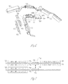
- FIG. 6 illustrates, by way of example and not limitation, a perspective view of a segmented design of a hearing assistance device.
- a first flex circuit segment 604 may function as a mainboard with a DSP processor package 611. The first flex circuit segment 604 may also have a radio package 612 configured to provide the hearing assistance device with wireless communication capabilities.
- a second flex circuit segment 605 may have a power management package 613, and a third flex circuit segment 606 may have one or more microphones 614, a telecoil ("t-coil”) 615, and a switch 616 configured to be manipulated by a user of the hearing assistance device.
- the first flex circuit segment 604 may include connector receptacles 607A and 608A.
- the second flex circuit segment 605 may include a connector plug 607B configured to cooperate with receptacle 607A to mechanically and electrically connect the first and second flex circuit 604 and 605.
- the third flex circuit segment 606 may include a connector plug 608B configured to cooperate with receptacle 608A to mechanically and electrically connect the first and third flex circuit segments 604 and 606.
- a stiffener board 618 may be mounted on the opposite surface of the flex circuit from the surface on which the connector element 607A, 607B, 608A, 608B is mounted.
- the footprint of the stiffener board 618 may be the same or approximately the same as the footprint of the connector element.
- the material of the stiffener board may be any rigid material that is not solid metal. Examples of such material include, but are not limited to, FR4 board, acrylic, epoxy, polyimide, kapton, ceramic, silicon, and the like.
- the rigid material may contain solder pads consisting of ENIG finish or other pad finishes.
- the rigid material may also contain small solder balls on top of the pads. The pads are not used for any electrical connection purposes, but rather are used as means for mechanically attaching the stiffener to the flexible substrate on the opposite side of the board-to-board connector.
- the rigid material can be supplied to the pick-and-place machine for mounting on the flexible electronics by a number of methods, including by way of example and not limitation, by tape and reel and waffle pack.
- the flexible circuit to which the rigid material will be attached contains solder pads to match those of the rigid material.
- solder balls on the rigid material flux is applied to the flexible circuit pads per the normal flux printing process and the stiffener attached during the normal pick and place process.
- solder paste is applied to the flexible circuit pads per the normal solder paste printing process and the stiffener attached during the normal pick and place process.
- the entire flexible circuit board is put through the reflow oven, during which all SMD(s) firmly attach to the circuit board, including the stiffener.
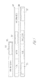
- FIG. 7 illustrates by way of example and not limitation, that SMD(s) 719 may be mounted on either major surface, and illustrates a connector element 707 on a surface and a stiffener board 718 on the opposite surface.
- the flex circuit may be assembled by mounting component(s) on one major surface of the flex circuit and then mounting component(s) on the other major surface of the flex circuit.
- the surface of the flex circuit may include a mounting pad, such as a solder pad, on which the component may be mounted to the surface.
- the process of mounting component(s) on a given surface may include mounting one or more SMD(s), a connector element or a stiffener board. That is, the connector element or stiffener board may be mounted on a surface of the flex circuit during the same process for mounting SMD(s) on the surface.
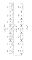
- FIG. 8 illustrates a flow diagram for assembling a two-sided flex assembly, which may also be referred to as a flexible circuit assembly or flex circuit assembly.
- the two-sided flex assembly may be a flex circuit segment for a larger segmented flex assembly.
- the diagram illustrates the assembly of side 1 (e.g. including mounting SMD(s) on first major surface) and then the assembly of side 2 (e.g. including mounting SMD(s) on a second major surface).
- the process steps provide a high-level view of the process for assembling a flex assembly, and the illustrated steps are the same for both surfaces of the flex assembly.
- Assembly of the first side of the flex circuit may include printing solder 820A and printing flux 821A on the first side of the flex substrate.
- a pick and place mechanism may be used to place the SMD(s) 822A (e.g. SMDs, connector elements, and/ or stiffener board) on the first side of the flex substrate according to the design of the system.
- the solder is reflowed 823A, and the assembly is cleaned 824A and baked 825A.
- an underfill may be applied and cured 826A.
- the second side of the flex circuit may be similarly assembled by printing solder 820B, printing flux 821B, picking and placing SMD(s) 822B, reflowing solder 823B, cleaning the assembly 824B, baking the assembly 825B, and applying an underfill and curing 826B.
- Various embodiments of the present subject matter provide flex assemblies with reinforced board-to-board connectors fabricated at the surface mounted device (SMD) level of the flex circuit.
- SMD surface mounted device
- the present subject matter improves the reliability of board-to-board connectors without altering the flex fabrication process and without implementing additional hand assembly steps.
- a different processing step is not required as the reinforcement may be applied using the same pick-and-place processing used to mount the devices on the flex assembly.
- a pick and place machine may automatically place the stiffener board on the flex circuit in the same fashion as other SMD(s) and the stiffener board is secured to the flex circuit by solder during the reflow process.
- previous methods would require additional frontend efforts by the circuit supplier or would require more manual processes, such in applying adhesive based attachments, after the SMD assembly process.
- FIG. 9 illustrates a flow diagram for assembling SMDs and connector elements in a flex assembly, which may also be referred to as a flex circuit, and further illustrates by way of example and not limitation that SMDs may be mounted on either major surface of the flexible substrates, and also illustrates a connector element and a stiffener board mounted on opposing surfaces.
- the flex circuit may be a flex circuit segment for a larger segmented flex assembly.
- the first side of the flex circuit is assembled 927A, and this process includes picking and placing components 922A on the surface of the first side.
- the second side of the flex circuit is assembled 927B, and this process similarly includes picking and placing components 922B.
- the components that are picked and placed may include one or more SMD(s), one or more connector element(s), or one or more stiffener board(s). All of the SMD(s) may be placed on the surface before the solder is reflowed.
- FIG. 10 illustrates, by way of example and not limitation, a footprint of a stiffener board 1018.
- the footprint is generally compatible with the footprint of a connector element.
- a rectangular stiffener board may be compatible with a rectangular connector element.
- the connector element may include larger solder bumps around the periphery of the connector element to provide mechanical coupling.
- the connector element may also include smaller solder bumps spaced closer together to provide electrical coupling between the connector and the flex circuit substrate.
- the stiffener may similarly include the larger solder bumps 1020 around the periphery to provide the mechanical connection.
- the stiffener board does not have an electrical function and thus does not include the smaller solder bumps.
- the stiffener material can have solder balls populated to mate with each pad, or only selectively populate some. The stiffener can then be underfilled per the normal process as well for extra support and pad protection.
- the size of stiffener material may be less than 25 mm 2 in some embodiments.
- the size of the stiffener material may be less than 10 mm 2 . In some embodiment, the size of the stiffener material may be less than 5 mm 2 .
- flex assemblies with board-to-board connectors to connect a flex or flex circuit assembly to another flex circuit or flex circuit assembly.
- these flex assemblies may be implemented in hearing assistance devices. It is understood that any hearing assistance device may be used without departing from the scope and the devices depicted in the figures are intended to demonstrate the subject matter, but not in a limited, exhaustive, or exclusive sense. It is also understood that the present subject matter can be used with a device designed for use in the right ear or the left ear or both ears of the wearer.
- hearing assistance devices include hearing aids
- hearing aids include but are not limited to, behind-the-ear (BTE), in-the-ear (ITE), in-the-canal (ITC), receiver-in-canal (RIC), or completely-in-the-canal (CIC) type hearing aids.
- BTE behind-the-ear
- ITE in-the-ear
- ITC in-the-canal
- RIC receiver-in-canal
- CIC completely-in-the-canal
- hearing aids may include devices that reside substantially behind the ear or over the ear.
- Such devices may include hearing aids with receivers associated with the electronics portion of the behind-the-ear device, or hearing aids of the type having receivers in the ear canal of the user, including but not limited to receiver-in-canal (RIC) or receiver-in-the-ear (RITE) designs.
- RIC receiver-in-canal
- RITE receiver-in-the-ear
- the present subject matter can also be used in hearing assistance devices generally, such as cochlear implant type hearing devices and such as deep insertion devices having a transducer, such as a receiver or microphone, whether custom fitted, standard, open fitted or occlusive fitted. It is understood that other hearing assistance devices not expressly stated herein may be used in conjunction with the present subject matter.
- digital hearing aids include a processor.
- a processor programmed to provide corrections to hearing impairments
- programmable gains are employed to tailor the hearing aid output to a wearer's particular hearing impairment.
- the processor may be a digital signal processor (DSP), microprocessor, microcontroller, other digital logic, or combinations thereof.
- DSP digital signal processor
- the processing of signals referenced in this application can be performed using the processor. Processing may be done in the digital domain, the analog domain, or combinations thereof. Processing may be done using subband processing techniques. Processing may be done with frequency domain or time domain approaches. Some processing may involve both frequency and time domain aspects.
- drawings may omit certain blocks that perform frequency synthesis, frequency analysis, analog-to-digital conversion, digital-to-analog conversion, amplification, and certain types of filtering and processing.
- the processor is adapted to perform instructions stored in memory which may or may not be explicitly shown.
- Various types of memory may be used, including volatile and nonvolatile forms of memory.
- instructions are performed by the processor to perform a number of signal processing tasks.
- analog components are in communication with the processor to perform signal tasks, such as microphone reception, or receiver sound embodiments (i.e., in applications where such transducers are used).
- different realizations of the block diagrams, circuits, and processes set forth herein may occur without departing from the scope of the present subject matter.
- the hearing assistance device may support wireless communications.
- the wireless communications can include standard or nonstandard communications.
- Some examples of standard wireless communications include link protocols including, but not limited to, BluetoothTM, IEEE 802.11(wireless LANs), 802.15 (WPANs), 802.16 (WiMAX), cellular protocols including, but not limited to CDMA and GSM, ZigBee, and ultra-wideband (UWB) technologies.
- Such protocols support radio frequency communications and some support infrared communications.
- the wireless communication maybe implemented using radio, ultrasonic, optical, or forms of wireless communication.
- the standards which can be used include past and present standards. It is also contemplated that future versions of these standards and new future standards may be employed without departing from the scope of the present subject matter.
- the wireless communications may support a connection from other devices.
- Such connections include, but are not limited to, one or more mono or stereo connections or digital connections having link protocols including, but not limited to 802.3 (Ethernet), 802.4, 802.5, USB, ATM, Fibre-channel, Firewire or 1394, InfiniBand, or a native streaming interface.
- link protocols including, but not limited to 802.3 (Ethernet), 802.4, 802.5, USB, ATM, Fibre-channel, Firewire or 1394, InfiniBand, or a native streaming interface.
- link protocols including, but not limited to 802.3 (Ethernet), 802.4, 802.5, USB, ATM, Fibre-channel, Firewire or 1394, InfiniBand, or a native streaming interface.
- such connections include all past and present link protocols. It is also contemplated that future versions of these protocols and new future standards may be employed without departing from the scope of the present subject matter.
- Hearing assistance devices typically include an enclosure or housing, a microphone, hearing assistance device electronics including processing electronics, and a speaker or receiver. It is understood that in various embodiments the microphone is optional. It is understood that in various embodiments the receiver is optional. Antenna configurations may vary and may be included within an enclosure for the electronics or be external to an enclosure for the electronics.
Landscapes
- Engineering & Computer Science (AREA)
- Microelectronics & Electronic Packaging (AREA)
- Manufacturing & Machinery (AREA)
- Health & Medical Sciences (AREA)
- General Health & Medical Sciences (AREA)
- Neurosurgery (AREA)
- Otolaryngology (AREA)
- Physics & Mathematics (AREA)
- Acoustics & Sound (AREA)
- Signal Processing (AREA)
- Combinations Of Printed Boards (AREA)
Description
- This document relates generally to flexible circuits and more particularly to flexible circuit assemblies with board-to-board connectors to connect a flexible circuit or flexible circuit assembly to another flexible circuit or flexible circuit assembly and a method to provide connector reinforcement.
- Flexible electronics, also referred to as flex assemblies, is a technology in which electronic devices may be mounted on flexible substrates. These devices mounted onto the flexible substrate may be referred to as surface mounted devices (SMDs). Examples of such substrates include but are not limited to polyimide or PEEK. The completed flexible electronic assembly may conform to a desired shape or may flex during use, such as may be desirable for tightly assembled electronic packages or where the assembly is required to flex during normal use. By way of example and not limitation, hearing aids or other hearing assistance devices may be fabricated using flexible electronics. Flexible electronics may be passive wiring structures used to interconnect integrated circuits and other electronic SMDs. Flexible electronics may be used to make interconnections to electronic assemblies directly or by use of connectors to a secondary electronic assembly.
- A segmented flex assembly may include more than one flex circuit segments. These flex circuit segments, which may be referred to as flex circuit boards, may be connected using board-to-board connectors. Board-to-board connectors may be surface mounted on to flexible circuits. Elements of a board-to-board connector may include a board-to-board connector plug and a complementary board-to-board connector receptacle. It is desirable to increase the robustness of these board-to-board connectors.
- Given the flexibility of the substrate on which the board-to-board connectors are attached, reliability issues may arise without a stiffener to support the flexible circuit in the location of the board-to-board connectors. For example, the lack of a stiffener may lead to bent or broken connectors during assembly and repair, and may lead to circuit delamination during the detaching process, with the connector tearing apart from the flex. A stiffener may be fabricated using a rigid material, such as polyethylene terephthalate (PET), FR4 board or stainless steel. PET is a thermoplastic polymer resin, and an FR4 board is a glass epoxy which has been used to fabricate printed circuit boards (PCBs). Generally the stiffener is either built into the board during the fabrication process or attached during subsequent assembly steps using an adhesive. Building the stiffener into the board during the fabrication process greatly increases the price of the flexible circuit assembly. Fabricating the stiffener into the board also reduces the circuit board's versatility, as the presence of the stiffener on one side limits the locations connectors can be attached and the resulting possible assembly orientations of the flexible circuit. A stiffener may be attached post assembly, but the additional assembly steps require additional time and materials. For example, common methods involve the use of either a thermoset or pressure sensitive adhesive. These methods are generally complicated, with the adhesives and stiffener boards supplied separately and combination completed in house by assembly operators.
- Underfilling may involve a process in which epoxy or other adhesives are applied under SMD(s) mounted on the flexible substrate, and then cured to harden. However, underfill cannot be effectively used to further reinforce the connector without the need for a stiffener, as underfilling can wick into the connectors, preventing them from making electrical connections and functioning properly.
- Accordingly, there is a need in the art for improving flexible circuit assemblies, including improving connections between boards of the flexible circuit assemblies.
- Disclosed herein, among other things, are systems and methods for reinforcing board-to-board connectors that connect a flexible circuit or flexible circuit assembly to another flexible circuit or flexible circuit assembly. By way of example, an embodiment of a system may include a first flexible substrate with a first number of conductors, the first flexible substrate configured to be mechanically flexed. The system may further include a surface mounted device (SMD) mounted on the first flexible substrate and connected to at least some of the first number of conductors, and a first board-to-board connector element connected to at least some of the first number of conductors on a first side of the substrate. The first board-to-board connector element is configured to mechanically connect to a second board-to-board connector element on a second flexible substrate and to electrically connect at least some of the first number of conductors in the first flexible substrate to at least some conductors in the second flexible substrate. The system may further include a stiffener board connected to a second side of the first or second flexible substrate opposite the board-to-board connector element by a solder connection.
- An embodiment of a system may comprise a first flex circuit segment and a second flex circuit segment. The first flex circuit segment may include a first flexible substrate with a first number of conductors, a first surface mounted device (SMD) mounted on the first flexible substrate and connected to at least some of the first number of conductors, a first board-to-board connector element on a first side of the first flexible substrate connected to at least some of the first number of conductors, and a first stiffener board connected to a second side of the first flexible substrate opposite the board-to-board connector element. The second flex circuit segment may include a second flexible substrate with a second number of conductors, a second SMD mounted on the second flexible substrate and connected to at least some of the second number of conductors, a second board-to-board connector element on a first side of the second flexible substrate connected to at least some of the second number of conductors , and a second stiffener board connected to a second side of the second flexible substrate opposite the board-to-board connector element. The first and second board-to-board connector elements are configured to mechanically connect to each and to electrically connect at least some of the first number of conductors to at least some of the second number of conductors.
- An embodiment of a method includes assembling a flex circuit, which may include assembling SMD(s) on a flexible substrate that has a first major surface and a second major surface. Assembling SMD(s) may include preparing mounting pads on the flexible substrate. The mounting pads includes at least a first mounting pad on the first major surface of the flexible substrate, at least a second mounting pad on the second major surface, the first and second mounting pads being on opposing sides of the flexible substrate to cause the first and second mounting pads to sandwich the flexible substrate, and at least one other mounting pad on the first major surface or the second major surface. The method may further include machine assisted, automatic picking and placing SMD(s) onto the mounting pads. The SMD(s) include at least one surface mounted device (SMD), a connection element and a stiffener board. At least one SMD may be mounted onto at least one other mounting pad. The connection element may be mounted to one of the first or the second mounting pads. A stiffener board maybe mounted to the other one of the first or second mounting pads.
- Further, the following constitute embodiments of the present invention:
- Embodiment 1: A system, comprising a first flexible substrate with a first number of conductors, the first flexible substrate configured to be mechanically flexed; a surface mounted device (SMD) mounted on the first flexible substrate and connected to at least some of the first number of conductors; a first board-to-board connector element connected to at least some of the first number of conductors on a first side of the substrate, the first board-to-board connector element being configured to mechanically connect to a second board-to-board connector element on a second flexible substrate and to electrically connect at least some of the first number of conductors in the first flexible substrate to at least some conductors in the second flexible substrate; and a stiffener board connected by a solder connection to a second side of the first flexible substrate opposite the board-to-board connector element.
- Embodiment 2: The system according to
embodiment 1, wherein the stiffener board includes a rigid material that is not solid metal. - Embodiment 3: The system according to
embodiment 1, wherein the stiffener board includes FR4 board, acrylic, epoxy, polyimide, kapton, ceramic, or silicon. - Embodiment 4: The system according to any of
embodiments 1 to 3, wherein the first board-to-board connector element includes one of a board-to-board connector plug or a board-to-board connector receptacle, and the second board-to-board connector element includes the other of the board-to-board connector plug or the board-to-board connector receptacle. - Embodiment 5: The system according to any of
embodiments 1 to 4, wherein the SMD is mounted on the first side of the first flexible substrate. - Embodiment 6: The system according to any of
embodiments 1 to 4, wherein the SMD is mounted on the second side of the first flexible substrate. - Embodiment 7: The system according to any of
embodiments 1 to 4, wherein the SMD is a first SMD mounted on the first side of the first flexible substrate, the system further including a second SMD mounted on the second side of the first flexible substrate. - Embodiment 8: The system according to any of
embodiment 1 to 7, wherein the stiffener board is configured to provide mechanical support without providing an electrical function for the system. - Embodiment 9: A system, comprising a first flex circuit segment, including a first flexible substrate with a first number of conductors, the first flexible substrate configured to be mechanically flexed; a first surface mounted device (SMD) mounted on the first flexible substrate and connected to at least some of the first number of conductors; a first board-to-board connector element on a first side of the first flexible substrate connected to at least some of the first number of conductors; and a first stiffener board connected by a solder connection to a second side of the first flexible substrate opposite the board-to-board connector element; and the system further comprising a second flex circuit segment, including a second flexible substrate with a second number of conductors, the second flexible substrate configured to be mechanically flexed; a second SMD mounted on the second flexible substrate and connected to at least some of the second number of conductors; a second board-to-board connector element on a first side of the second flexible substrate connected to at least some of the second number of conductors, wherein the first and second board-to-board connector elements are configured to mechanically connect to each and to electrically connect at least some of the first number of conductors to at least some of the second number of conductors; and a second stiffener board connected by a solder connection to a second side of the second flexible substrate opposite the board-to-board connector element.
- Embodiment 10: The system according to embodiment 9, wherein a first mounting pad is used to mount the first board-to-board connector element to the first side of the first flexible substrate, and a second mounting pad is used to mount the second board-to-board connector element to the second side of the first flexible substrate, and wherein the first mounting pad and the second mounting pad have compatible designs with identical footprints, and wherein outer solder balls are used to mechanically connect the first board-to-board connector element to the first mounting pad.
- Embodiment 11: The system according to any of embodiments 9 to 10, wherein each of the first and second flexible substrates have a rectangular footprint.
- Embodiment 12: The system according to any of embodiments 9 to 11, wherein the system is a hearing assistance system, the first flex circuit segment includes a main board, and the second flex circuit segment includes at least one microphone.
- Embodiment 13: The system according to embodiment 12, wherein the first connector element mounted to the main board is a board-to-board connector receptacle, and wherein the main board includes another board-to-board connector receptacle mounted to one of the first or second sides, and another stiffener board mounted to the other of the first or second sides.
- Embodiment 14: The system according to any of embodiments 9 to 13, wherein each of the first and second stiffener boards includes a rigid material that is not solid metal.
- Embodiment 15: A method, comprising assembling a flex circuit, wherein assembling the flexible circuit includes assembling SMD(s) on a flexible substrate that has a first major surface and a second major surface, including preparing mounting pads on the flexible substrate, the mounting pads including at least a first mounting pad on the first major surface of the flexible substrate; at least a second mounting pad on the second major surface, the first and second mounting pads being on opposing sides of the flexible substrate to cause the first and second mounting pads to sandwich the flexible substrate; and at least one other mounting pad on the first major surface or the second major surface; the assembling further including picking and placing SMD(s) onto the mounting pads, the SMD(s) including at least one surface mounted device (SMD), a connection element and a stiffener board, the at least one SMD being mounted onto the at least one other mounting pad, the connection element being mounted to one of the first or the second mounting pads, and a stiffener board being mounted to the other one of the first or second mounting pads.
- Embodiment 16: The method according to embodiment 15, wherein preparing mounting pads includes printing solder or printing flux or both printing solder and printing flux on the mounting pads, the method further comprising reflowing the solder after picking and placing the SMD(s) on the mounting pads.
- Embodiment 17: The method according to any of embodiments 15 to 16, wherein assembling the flexible circuit includes assembling SMD(s) onto the first major surface of the flexible substrate, including printing solder on mounting pads on the first major surface; printing flux on the mounting pads on the first major surface; picking and placing SMD(s) onto the mounting pads on the first major surface to create a first intermediate structure with SMD(s) on the first mounting pads; cleaning the first intermediate structure, baking the cleaned first intermediate structure and then applying underfill and curing the baked first intermediate structure; and applying underfill and curing the structure; and wherein assembling the flexible circuit further includes assembling SMD(s) onto the second major surface of the flexible substrate, including printing solder on mounting pads on the second major surface; printing flux on the mounting pads on the second major surface; picking and placing SMD(s) onto the mounting pads on the first major surface to create a second intermediate structure with SMD(s) on the mounting pads on the second surface; cleaning the second intermediate structure, baking the cleaned second intermediate structure and then applying underfill and curing the baked second intermediate structure.
- Embodiment 18: The method according to any of embodiments 15 to 17, wherein the connection element is configured to mechanically connect to another connection element on another flexible substrate and to electrically connect at least some conductors in the first flexible substrate to at least some conductors in the second flexible substrate.
- Embodiment 19: The method according to embodiment 18, wherein the connection element is one of a plug or a receptacle, and the other connection element is the other one of the plug or the receptacle.
- Embodiment 20: The method according to any of embodiments 15 to 19, wherein picking and placing SMD(s) includes supplying stiffener boards to a pick and place machine using a waffle pack or using a tape and reel.
- This Summary is an overview of some of the teachings of the present application and not intended to be an exclusive or exhaustive treatment of the present subject matter. Further details about the present subject matter are found in the detailed description and appended claims. The scope of the present invention is defined by the appended claims and their legal equivalents.
-
-
FIG. 1 illustrates, by way of example and not limitation, flex circuits and a board-to-board connector mating pair between flex circuits. -
FIG. 2 illustrates, by way of example and not limitation, a segmented system fabricated using flex circuits and multiple board-to-board mating pairs. -
FIG. 3 illustrates, by way of example and not limitation, another connection arrangement of the flex circuits ofFIG. 2 . -
FIG. 4 illustrates, by way of example and not limitation, a segmented design implemented using flex circuits for a hearing assistance device. -
FIG. 5 illustrates, by way of example and not limitation, a planar view of the flex circuit segments ofFIG. 4 . -
FIG. 6 illustrates, by way of example and not limitation, a perspective view of a segmented design of a hearing assistance device. -
FIG. 7 illustrates by way of example and not limitation that SMDs may be mounted on either major surface of the flexible substrates, and illustrates a connector element on a surface and a stiffener board on the opposite surface. -
FIG. 8 illustrates a flow diagram for assembling a two-sided flex assembly, which may also be referred to as a flexible circuit assembly or a flex circuit assembly. -
FIG. 9 illustrates a flow diagram for assembling SMDs and connector elements in a flex assembly, which also may be referred to as a flex circuit, and further illustrates by way of example and not limitation that SMDs may be mounted on either major surface of the flexible substrates, and also illustrates a connector element and a stiffener board mounted on opposing surfaces. -
FIG. 10 illustrates, by way of example and not limitation, a footprint of a stiffener board. - The following detailed description of the present subject matter refers to subject matter in the accompanying drawings which show, by way of illustration, specific aspects and embodiments in which the present subject matter may be practiced. These embodiments are described in sufficient detail to enable those skilled in the art to practice the present subject matter. References to "an", "one", or "various" embodiments in this disclosure are not necessarily to the same embodiment, and such references contemplate more than one embodiment. The following detailed description is demonstrative and not to be taken in a limiting sense. The scope of the present subject matter is defined by the appended claims, along with the full scope of legal equivalents to which such claims are entitled.
- This document refers generally to flexible circuits or flexible circuit assemblies. Flexible circuit assemblies may include one or more flexible substrates that may be connected to each other to form the assembly. Each flexible substrate and the circuitry and the SMDs thereon may be referred to as a flexible circuit or flexible circuit assembly or more simply as a flex circuit or flex assembly.
-
FIG. 1 illustrates, by way of example and not limitation, flex circuits and a board-to-board connector mating pair between flex circuits. Each of theflex circuits board connector elements 103A-B attached thereon. The board-to-board connector elements are configured to mechanically connect the flexible substrates and to electrically connect at least some of the conductors in the flexible substrate of theflex circuit 101 to at least some conductors in the flexible substrate of theflex circuit 102. Theconnector elements 103A-B may have a cooperative relationship such as a plug / receptacle relationship. - The flexible substrates may be cut from a panel of flex (e.g. a panel of two- layer flex or a panel of four-layer flex by way of example), depending on the design of the flex circuit assembly. The cut flexible substrates have two major surfaces (e.g. a top surface and a bottom surface). SMD(s) may be mounted to either major surface or some SMD(s) may be mounted on one surface and other SMD(s) may be mounted on the other surface. The final design of the flexible circuit may be segmental, in which multiple flex circuits connect together to form a final flex assembly. One or more SMD(s) may be on one of the flexible substrates, and one or more SMD(s) may be on another of the flexible substrates.
-
FIG. 2 illustrates, by way of example and not limitation, a segmented system fabricated using flex circuits and multiple board-to-board mating pairs. The illustrated system forms a flex assembly using a firstflex circuit segment 204, a secondflex segment circuit 205, and a thirdflex segment circuit 206, where each flex circuit segment has one or more SMD(s) mounted thereon.FIG. 2 illustratesconnector elements 207A-B for connecting the firstflex circuit segment 204 to the secondflex circuit segment 205, and further illustratesconnector elements 208A-B for connecting the firstflex circuit segment 204 to the thirdflex circuit segment 206. Each of the flex circuit segments also includes at least one area in which a board-to-board connector element may be mounted. This area may be referred to as a mounting pad area. An example of a mounting pad area is a solder pad. In some embodiments, the flex circuit may be designed to allow a board-to-board connector element to be mounted on either major surface (i.e. either on the top surface or bottom surface) in the same area of the flex circuit. Thus, for example, board-to-board connector element 207A may be positioned at 209A on the other major surface of the firstflex circuit segment 204, and/or board-to-board connector element 207B may be positioned at 209B on the other major surface of the secondflex circuit segment 205. Also, board-to-board connector element 208A may be positioned at 210A on the other major surface of the firstflex circuit segment 204, and/or board-to-board connector element 208B may be positioned at 210B on the other major surface of the thirdflex circuit segment 206. This capability provides flexibility in working with the segmented design of the flex circuits when assembling the flex circuits into the completed flex circuit assembly. By way of example and not limitation,FIG. 3 illustrates another connection arrangement of the flex circuits ofFIG. 2 . As illustrated, the thirdflex circuit segment 206 is connected on top of the firstflex circuit segment 204 usingconnectors 208A-B. -
FIG. 4 illustrates, by way of example and not limitation, a segmented design using flex circuits for a hearing assistance device. A firstflex circuit segment 304 may function as a mainboard with aDSP processor package 311. The firstflex circuit segment 304 may also have aradio package 312 configured to provide the hearing assistance device with wireless communication capabilities. A secondflex circuit segment 305 may also have apower management package 313, and athird flex circuit 306 may have one ormore microphones 314, a telecoil ("t-coil") 315, and aswitch 316 configured to be manipulated by a user of the hearing assistance device. The telecoil 315 may be designed to pick up an electromagnetic signal for conversion to a sound for presentation to the user, and the switch may be configured to allow the user to change whether the sound presented to the user is the ambient sound or a sound converted from the electromagnetic signal. Each of these modules may be implemented in a number of hearing assistance device designs, including different hearing aid styles such as behind-the-ear or receiver-in-canal designs, and including left and right hearing aids. For example, the ability to connect on either side of a flex circuit may allow a flex circuit to be assembled in a right hearing aid or a symmetrical left hearing aid. The flex circuit segments of the flexible circuit assembly may be flipped or folded differently. -
FIG. 5 illustrates, by way of example and not limitation, a planar view of the flex circuit segments ofFIG. 4 . If the flexible substrate has a rectangular footprint rather than a more irregular shape, more flexible substrates may be cut from a given panel of flex. Any segment may be on either major surface of corresponding flexible substrate. Flexible circuits may be designed with connector footprints on both sides of the circuit, allowing for a connector to be attached to either side. These footprints may be referred to as aconnector area 317 used to mount a connector element (e.g. connector plug or connector receptacle). For example, the flexible circuit may be designed for use within a variety of hearing aids, and to fit within a behind-the-ear hearing aid with the connector on one side of the circuit and to fit within a receiver-in-canal hearing aid with the connector on the other side of the circuit, thus increasing the circuits re-usability. Theconnector area 317 may be a solder pad on which the connector element or stiffener board may be mounted. Thus, according to various embodiments, a connector element (e.g. plug or receptacle) may be mounted in thisarea 317 on one of the major surfaces, and a stiffener board may be mounted in thisarea 317 on the other one of the major surfaces. -
FIG. 6 illustrates, by way of example and not limitation, a perspective view of a segmented design of a hearing assistance device. A firstflex circuit segment 604 may function as a mainboard with aDSP processor package 611. The firstflex circuit segment 604 may also have aradio package 612 configured to provide the hearing assistance device with wireless communication capabilities. A secondflex circuit segment 605 may have apower management package 613, and a thirdflex circuit segment 606 may have one ormore microphones 614, a telecoil ("t-coil") 615, and aswitch 616 configured to be manipulated by a user of the hearing assistance device. The firstflex circuit segment 604 may includeconnector receptacles flex circuit segment 605 may include aconnector plug 607B configured to cooperate withreceptacle 607A to mechanically and electrically connect the first andsecond flex circuit flex circuit segment 606 may include aconnector plug 608B configured to cooperate withreceptacle 608A to mechanically and electrically connect the first and thirdflex circuit segments stiffener board 618 may be mounted on the opposite surface of the flex circuit from the surface on which theconnector element stiffener board 618 may be the same or approximately the same as the footprint of the connector element. - The material of the stiffener board may be any rigid material that is not solid metal. Examples of such material include, but are not limited to, FR4 board, acrylic, epoxy, polyimide, kapton, ceramic, silicon, and the like. The rigid material may contain solder pads consisting of ENIG finish or other pad finishes. The rigid material may also contain small solder balls on top of the pads. The pads are not used for any electrical connection purposes, but rather are used as means for mechanically attaching the stiffener to the flexible substrate on the opposite side of the board-to-board connector. The rigid material can be supplied to the pick-and-place machine for mounting on the flexible electronics by a number of methods, including by way of example and not limitation, by tape and reel and waffle pack. The flexible circuit to which the rigid material will be attached contains solder pads to match those of the rigid material. In the case of solder balls on the rigid material, flux is applied to the flexible circuit pads per the normal flux printing process and the stiffener attached during the normal pick and place process. In the case of no solder balls and only solder pads on the stiffener, solder paste is applied to the flexible circuit pads per the normal solder paste printing process and the stiffener attached during the normal pick and place process. The entire flexible circuit board is put through the reflow oven, during which all SMD(s) firmly attach to the circuit board, including the stiffener.
-
FIG. 7 illustrates by way of example and not limitation, that SMD(s) 719 may be mounted on either major surface, and illustrates aconnector element 707 on a surface and astiffener board 718 on the opposite surface. The flex circuit may be assembled by mounting component(s) on one major surface of the flex circuit and then mounting component(s) on the other major surface of the flex circuit. The surface of the flex circuit may include a mounting pad, such as a solder pad, on which the component may be mounted to the surface. The process of mounting component(s) on a given surface may include mounting one or more SMD(s), a connector element or a stiffener board. That is, the connector element or stiffener board may be mounted on a surface of the flex circuit during the same process for mounting SMD(s) on the surface. -
FIG. 8 illustrates a flow diagram for assembling a two-sided flex assembly, which may also be referred to as a flexible circuit assembly or flex circuit assembly. The two-sided flex assembly may be a flex circuit segment for a larger segmented flex assembly. The diagram illustrates the assembly of side 1 (e.g. including mounting SMD(s) on first major surface) and then the assembly of side 2 (e.g. including mounting SMD(s) on a second major surface). The process steps provide a high-level view of the process for assembling a flex assembly, and the illustrated steps are the same for both surfaces of the flex assembly. Assembly of the first side of the flex circuit may includeprinting solder 820A andprinting flux 821A on the first side of the flex substrate. A pick and place mechanism may be used to place the SMD(s) 822A (e.g. SMDs, connector elements, and/ or stiffener board) on the first side of the flex substrate according to the design of the system. After placing the SMD(s), the solder is reflowed 823A, and the assembly is cleaned 824A and baked 825A. Finally, an underfill may be applied and cured 826A. The second side of the flex circuit may be similarly assembled by printingsolder 820B,printing flux 821B, picking and placing SMD(s) 822B, reflowingsolder 823B, cleaning theassembly 824B, baking theassembly 825B, and applying an underfill and curing 826B. - Various embodiments of the present subject matter provide flex assemblies with reinforced board-to-board connectors fabricated at the surface mounted device (SMD) level of the flex circuit. By performing this reinforcement during the SMD assembly process, the present subject matter improves the reliability of board-to-board connectors without altering the flex fabrication process and without implementing additional hand assembly steps. Further, a different processing step is not required as the reinforcement may be applied using the same pick-and-place processing used to mount the devices on the flex assembly. For example, a pick and place machine may automatically place the stiffener board on the flex circuit in the same fashion as other SMD(s) and the stiffener board is secured to the flex circuit by solder during the reflow process. In contrast, previous methods would require additional frontend efforts by the circuit supplier or would require more manual processes, such in applying adhesive based attachments, after the SMD assembly process.
-
FIG. 9 illustrates a flow diagram for assembling SMDs and connector elements in a flex assembly, which may also be referred to as a flex circuit, and further illustrates by way of example and not limitation that SMDs may be mounted on either major surface of the flexible substrates, and also illustrates a connector element and a stiffener board mounted on opposing surfaces. The flex circuit may be a flex circuit segment for a larger segmented flex assembly. The first side of the flex circuit is assembled 927A, and this process includes picking and placingcomponents 922A on the surface of the first side. The second side of the flex circuit is assembled 927B, and this process similarly includes picking and placingcomponents 922B. Depending on the design of the system, the components that are picked and placed may include one or more SMD(s), one or more connector element(s), or one or more stiffener board(s). All of the SMD(s) may be placed on the surface before the solder is reflowed. -
FIG. 10 illustrates, by way of example and not limitation, a footprint of astiffener board 1018. The footprint is generally compatible with the footprint of a connector element. By way of example and not limitation, a rectangular stiffener board may be compatible with a rectangular connector element. The connector element may include larger solder bumps around the periphery of the connector element to provide mechanical coupling. The connector element may also include smaller solder bumps spaced closer together to provide electrical coupling between the connector and the flex circuit substrate. The stiffener may similarly include thelarger solder bumps 1020 around the periphery to provide the mechanical connection. However, according to some embodiments, the stiffener board does not have an electrical function and thus does not include the smaller solder bumps. The stiffener material can have solder balls populated to mate with each pad, or only selectively populate some. The stiffener can then be underfilled per the normal process as well for extra support and pad protection. The size of stiffener material may be less than 25 mm2 in some embodiments. The size of the stiffener material may be less than 10 mm2. In some embodiment, the size of the stiffener material may be less than 5 mm2. - This document relates to flex assemblies with board-to-board connectors to connect a flex or flex circuit assembly to another flex circuit or flex circuit assembly. As identified above, these flex assemblies may be implemented in hearing assistance devices. It is understood that any hearing assistance device may be used without departing from the scope and the devices depicted in the figures are intended to demonstrate the subject matter, but not in a limited, exhaustive, or exclusive sense. It is also understood that the present subject matter can be used with a device designed for use in the right ear or the left ear or both ears of the wearer.
- Examples of hearing assistance devices include hearing aids, and examples of hearing aids include but are not limited to, behind-the-ear (BTE), in-the-ear (ITE), in-the-canal (ITC), receiver-in-canal (RIC), or completely-in-the-canal (CIC) type hearing aids. It is understood that behind-the-ear type hearing aids may include devices that reside substantially behind the ear or over the ear. Such devices may include hearing aids with receivers associated with the electronics portion of the behind-the-ear device, or hearing aids of the type having receivers in the ear canal of the user, including but not limited to receiver-in-canal (RIC) or receiver-in-the-ear (RITE) designs. The present subject matter can also be used in hearing assistance devices generally, such as cochlear implant type hearing devices and such as deep insertion devices having a transducer, such as a receiver or microphone, whether custom fitted, standard, open fitted or occlusive fitted. It is understood that other hearing assistance devices not expressly stated herein may be used in conjunction with the present subject matter.
- It is understood that digital hearing aids include a processor. In digital hearing aids with a processor programmed to provide corrections to hearing impairments, programmable gains are employed to tailor the hearing aid output to a wearer's particular hearing impairment. The processor may be a digital signal processor (DSP), microprocessor, microcontroller, other digital logic, or combinations thereof. The processing of signals referenced in this application can be performed using the processor. Processing may be done in the digital domain, the analog domain, or combinations thereof. Processing may be done using subband processing techniques. Processing may be done with frequency domain or time domain approaches. Some processing may involve both frequency and time domain aspects. For brevity, in some examples drawings may omit certain blocks that perform frequency synthesis, frequency analysis, analog-to-digital conversion, digital-to-analog conversion, amplification, and certain types of filtering and processing. In various embodiments the processor is adapted to perform instructions stored in memory which may or may not be explicitly shown. Various types of memory may be used, including volatile and nonvolatile forms of memory. In various embodiments, instructions are performed by the processor to perform a number of signal processing tasks. In such embodiments, analog components are in communication with the processor to perform signal tasks, such as microphone reception, or receiver sound embodiments (i.e., in applications where such transducers are used). In various embodiments, different realizations of the block diagrams, circuits, and processes set forth herein may occur without departing from the scope of the present subject matter.
- It is understood that the hearing assistance device may support wireless communications. In various embodiments the wireless communications can include standard or nonstandard communications. Some examples of standard wireless communications include link protocols including, but not limited to, Bluetooth™, IEEE 802.11(wireless LANs), 802.15 (WPANs), 802.16 (WiMAX), cellular protocols including, but not limited to CDMA and GSM, ZigBee, and ultra-wideband (UWB) technologies. Such protocols support radio frequency communications and some support infrared communications. The wireless communication maybe implemented using radio, ultrasonic, optical, or forms of wireless communication. It is understood that the standards which can be used include past and present standards. It is also contemplated that future versions of these standards and new future standards may be employed without departing from the scope of the present subject matter. The wireless communications may support a connection from other devices. Such connections include, but are not limited to, one or more mono or stereo connections or digital connections having link protocols including, but not limited to 802.3 (Ethernet), 802.4, 802.5, USB, ATM, Fibre-channel, Firewire or 1394, InfiniBand, or a native streaming interface. In various embodiments, such connections include all past and present link protocols. It is also contemplated that future versions of these protocols and new future standards may be employed without departing from the scope of the present subject matter.
- Hearing assistance devices typically include an enclosure or housing, a microphone, hearing assistance device electronics including processing electronics, and a speaker or receiver. It is understood that in various embodiments the microphone is optional. It is understood that in various embodiments the receiver is optional. Antenna configurations may vary and may be included within an enclosure for the electronics or be external to an enclosure for the electronics.
- This application is intended to cover adaptations or variations of the present subject matter. It is to be understood that the above description is intended to be illustrative, and not restrictive. The scope of the present subject matter should be determined with reference to the appended claims, along with the full scope of legal equivalents to which such claims are entitled.
Claims (15)
- A system, comprising:a first flexible substrate with a first number of conductors, the first flexible substrate configured to be mechanically flexed;a surface mounted device (SMD) mounted on the first flexible substrate and connected to at least some of the first number of conductors;a first board-to-board connector element connected to at least some of the first number of conductors on a first side of the substrate, the first board-to-board connector element being configured to mechanically connect to a second board-to-board connector element on a second flexible substrate and to electrically connect at least some of the first number of conductors in the first flexible substrate to at least some conductors in the second flexible substrate; anda stiffener board connected by a solder connection to a second side of the first flexible substrate opposite the board-to-board connector element.
- The system according to claim 1, wherein the stiffener board includes a rigid material that is not solid metal.
- The system according to claim 1, wherein the stiffener board includes FR4 board, acrylic, epoxy, polyimide, kapton, ceramic, or silicon.
- The system according to any of the preceding claims, wherein the first board-to-board connector element includes one of a board-to-board connector plug or a board-to-board connector receptacle, and the second board-to-board connector element includes the other of the board-to-board connector plug or the board-to-board connector receptacle.
- The system according to any of the preceding claims, wherein the stiffener board is configured to provide mechanical support without providing an electrical function for the system.
- The system according to claim 1, comprising:a first flex circuit segment, including the first flexible substrate, the surface mounted device (SMD) as a first SMD, the first board-to-board connector element, and the stiffener board as a first stiffener board; anda second flex circuit segment, including:a second flexible substrate with a second number of conductors, the second flexible substrate configured to be mechanically flexed;a second SMD mounted on the second flexible substrate and connected to at least some of the second number of conductors;a second board-to-board connector element on a first side of the second flexible substrate connected to at least some of the second number of conductors, wherein the first and second board-to-board connector elements are configured to mechanically connect to each and to electrically connect at least some of the first number of conductors to at least some of the second number of conductors; anda second stiffener board connected by a solder connection to a second side of the second flexible substrate opposite the board-to-board connector element.
- The system according to claim 6, wherein a first mounting pad is used to mount the first board-to-board connector element to the first side of the first flexible substrate, and a second mounting pad is used to mount the second board-to-board connector element to the second side of the first flexible substrate, and wherein the first mounting pad and the second mounting pad have compatible designs with identical footprints, and wherein outer solder balls are used to mechanically connect the first board-to-board connector element to the first mounting pad.
- The system according to any of claims 6-7, wherein each of the first and second flexible substrates have a rectangular footprint.
- The system according to any of claims 6-8, wherein the system is a hearing assistance system, the first flex circuit segment includes a main board, and the second flex circuit segment includes at least one microphone.
- The system according to claim 9, wherein the first connector element mounted to the main board is a board-to-board connector receptacle, and wherein the main board includes another board-to-board connector receptacle mounted to one of the first or second sides, and another stiffener board mounted to the other of the first or second sides.
- The system according to any of claims 6-10, wherein each of the first and second stiffener boards includes a rigid material that is not solid metal.
- A method, comprising:assembling a flex circuit, wherein assembling the flexible circuit includes assembling SMD(s) on a flexible substrate that has a first major surface and a second major surface, including:preparing mounting pads on the flexible substrate, the mounting pads including:at least a first mounting pad on the first major surface of the flexible substrate;at least a second mounting pad on the second major surface, the first and second mounting pads being on opposing sides of the flexible substrate to cause the first and second mounting pads to sandwich the flexible substrate; andat least one other mounting pad on the first major surface or the second major surface;picking and placing SMD(s) onto the mounting pads, the SMD(s) including at least one surface mounted device (SMD), a connection element and a stiffener board, the at least one SMD being mounted onto the at least one other mounting pad, the connection element being mounted to one of the first or the second mounting pads, and a stiffener board being mounted to the other one of the first or second mounting pads.
- The method according to claim 12, wherein preparing mounting pads includes printing solder or printing flux or both printing solder and printing flux on the mounting pads, the method further comprising reflowing the solder after picking and placing the SMD(s) on the mounting pads.
- The method according to any of claims 12-13, wherein assembling the flexible circuit includes:assembling SMD(s) onto the first major surface of the flexible substrate, including:printing solder on mounting pads on the first major surface;printing flux on the mounting pads on the first major surface;picking and placing SMD(s) onto the mounting pads on the first major surface to create a first intermediate structure with SMD(s) on the first mounting pads;cleaning the first intermediate structure, baking the cleaned first intermediate structure and then applying underfill and curing the baked first intermediate structure; andapplying underfill and curing the structure; andassembling SMD(s) onto the second major surface of the flexible substrate, including:printing solder on mounting pads on the second major surface;printing flux on the mounting pads on the second major surface;picking and placing SMD(s) onto the mounting pads on the first major surface to create a second intermediate structure with SMD(s) on the mounting pads on the second surface;cleaning the second intermediate structure, baking the cleaned second intermediate structure and then applying underfill and curing the baked second intermediate structure.
- The method according to any of claims 12-14, wherein picking and placing SMD(s) includes supplying stiffener boards to a pick and place machine using a waffle pack or using a tape and reel.
Applications Claiming Priority (1)
| Application Number | Priority Date | Filing Date | Title |
|---|---|---|---|
| US14/335,513 US9474154B2 (en) | 2014-07-18 | 2014-07-18 | Reflow solderable flexible circuit board — to — flexible circuit board connector reinforcement |
Publications (2)
| Publication Number | Publication Date |
|---|---|
| EP2975915A1 true EP2975915A1 (en) | 2016-01-20 |
| EP2975915B1 EP2975915B1 (en) | 2019-10-02 |
Family
ID=53673840
Family Applications (1)
| Application Number | Title | Priority Date | Filing Date |
|---|---|---|---|
| EP15177399.1A Active EP2975915B1 (en) | 2014-07-18 | 2015-07-17 | Reflow solderable flexible circuit board - to - flexible circuit board connector reinforcement |
Country Status (3)
| Country | Link |
|---|---|
| US (1) | US9474154B2 (en) |
| EP (1) | EP2975915B1 (en) |
| DK (1) | DK2975915T3 (en) |
Cited By (4)
| Publication number | Priority date | Publication date | Assignee | Title |
|---|---|---|---|---|
| US9782096B2 (en) | 2011-01-31 | 2017-10-10 | Clothing Plus Mbu Oy | Textile substrate for measuring physical quantity |
| CN107959915A (en) * | 2016-10-18 | 2018-04-24 | 西万拓私人有限公司 | Hearing aid and the signal processing apparatus for hearing aid |
| EP3806486A4 (en) * | 2018-05-30 | 2021-11-17 | Sony Group Corporation | INFORMATION PROCESSING DEVICE |
| US11291409B2 (en) | 2014-12-03 | 2022-04-05 | Clothing Plus Mbu Oy | Device for determining effects of aging of a wearable device |
Families Citing this family (15)
| Publication number | Priority date | Publication date | Assignee | Title |
|---|---|---|---|---|
| US11266014B2 (en) | 2008-02-14 | 2022-03-01 | Metrospec Technology, L.L.C. | LED lighting systems and method |
| US10334735B2 (en) | 2008-02-14 | 2019-06-25 | Metrospec Technology, L.L.C. | LED lighting systems and methods |
| US8851356B1 (en) * | 2008-02-14 | 2014-10-07 | Metrospec Technology, L.L.C. | Flexible circuit board interconnection and methods |
| US8007286B1 (en) | 2008-03-18 | 2011-08-30 | Metrospec Technology, Llc | Circuit boards interconnected by overlapping plated through holes portions |
| US9525222B2 (en) | 2014-04-11 | 2016-12-20 | Apple Inc. | Reducing or eliminating board-to-board connectors |
| US20160029503A1 (en) * | 2014-07-22 | 2016-01-28 | Apple Inc. | Reducing or eliminating board-to-board connectors |
| US9666967B2 (en) | 2014-07-28 | 2017-05-30 | Apple Inc. | Printed circuit board connector for non-planar configurations |
| US10945664B1 (en) | 2015-09-30 | 2021-03-16 | Apple, Inc. | Protective case with coupling gasket for a wearable electronic device |
| US10103688B2 (en) * | 2016-09-29 | 2018-10-16 | Sunpower Corporation | Systems and methods for improved installation and grounding of photovoltaic assemblies |
| US10085097B2 (en) | 2016-10-04 | 2018-09-25 | Starkey Laboratories, Inc. | Hearing assistance device incorporating system in package module |
| CN108076584B (en) * | 2016-11-15 | 2020-04-14 | 鹏鼎控股(深圳)股份有限公司 | Flexible circuit board, circuit board element and manufacturing method of flexible circuit board |
| CN106790792B (en) * | 2016-12-08 | 2019-02-05 | Oppo广东移动通信有限公司 | Imaging modules and mobile terminals |
| CN107817633A (en) * | 2017-10-26 | 2018-03-20 | 惠科股份有限公司 | Signal transmission device and display device |
| WO2019164310A1 (en) | 2018-02-21 | 2019-08-29 | Samsung Electronics Co., Ltd. | Electronic device including shield member for shielding at least part of magnetic force generated by magnetic substance and connection portion including property of nonmagnetic substance connected to shield member |
| US10849200B2 (en) | 2018-09-28 | 2020-11-24 | Metrospec Technology, L.L.C. | Solid state lighting circuit with current bias and method of controlling thereof |
Citations (7)
| Publication number | Priority date | Publication date | Assignee | Title |
|---|---|---|---|---|
| US4756940A (en) * | 1986-03-25 | 1988-07-12 | Tektronix, Inc. | Flexible circuit strain relief |
| US5201671A (en) * | 1992-01-24 | 1993-04-13 | Compaq Computer Corporation | Flex pull tab for surface mount connector |
| US5616050A (en) * | 1995-01-19 | 1997-04-01 | Ast Research Inc. | Flexible circuit connector |
| US20040081328A1 (en) * | 1996-03-14 | 2004-04-29 | Sarnoff Corporation | Hearing aid |
| US20070177749A1 (en) * | 2006-01-30 | 2007-08-02 | Sjursen Walter P | Hearing aid circuit with integrated switch and battery |
| US20090186496A1 (en) * | 2008-01-17 | 2009-07-23 | Hon Hai Precision Ind. Co., Ltd. | Board-to-board connector assembly having pull tab |
| US20130294628A1 (en) * | 2012-05-07 | 2013-11-07 | Starkey Laboratories, Inc. | Flex connector for a hearing assistance device |
Family Cites Families (49)
| Publication number | Priority date | Publication date | Assignee | Title |
|---|---|---|---|---|
| US5995855A (en) * | 1998-02-11 | 1999-11-30 | Masimo Corporation | Pulse oximetry sensor adapter |
| US5482473A (en) * | 1994-05-09 | 1996-01-09 | Minimed Inc. | Flex circuit connector |
| JP2746171B2 (en) * | 1995-02-21 | 1998-04-28 | 日本電気株式会社 | Solid-state imaging device and manufacturing method thereof |
| US5603619A (en) * | 1995-07-20 | 1997-02-18 | Intel Corporation | Scalable test interface port |
| US5903059A (en) | 1995-11-21 | 1999-05-11 | International Business Machines Corporation | Microconnectors |
| TW392976U (en) * | 1998-12-23 | 2000-06-01 | Hon Hai Prec Ind Co Ltd | Electrical connector assembly |
| JP3795706B2 (en) * | 1999-07-02 | 2006-07-12 | 富士通株式会社 | Connector for signal transmission path |
| US6462955B1 (en) * | 1999-09-13 | 2002-10-08 | Miraco, Inc. | Component alignment casing system |
| KR100597812B1 (en) * | 1999-09-20 | 2006-07-06 | 엘지.필립스 엘시디 주식회사 | Auxiliary connector of liquid crystal display |
| AU2001232772A1 (en) * | 2000-01-20 | 2001-07-31 | Gryphics, Inc. | Flexible compliant interconnect assembly |
| US7247932B1 (en) | 2000-05-19 | 2007-07-24 | Megica Corporation | Chip package with capacitor |
| US6299476B1 (en) * | 2000-10-04 | 2001-10-09 | Fci Usa, Inc. | Electrical connector with a flexible circuit and rigidizer subassembly and a spring |
| US6508661B1 (en) * | 2001-12-17 | 2003-01-21 | Hon Hai Precision Ind. Co., Ltd. | Flexible printed circuit connector |
| GB2388468B (en) | 2002-02-08 | 2005-05-04 | Microsaic Systems Ltd | Microengineered electrical connectors |
| JP4145226B2 (en) * | 2002-12-26 | 2008-09-03 | 第一電子工業株式会社 | connector |
| JP4543772B2 (en) * | 2003-09-19 | 2010-09-15 | セイコーエプソン株式会社 | Electro-optical device and electronic apparatus |
| US7025619B2 (en) | 2004-02-13 | 2006-04-11 | Zyvex Corporation | Sockets for microassembly |
| JP4014575B2 (en) * | 2004-03-29 | 2007-11-28 | シャープ株式会社 | Circuit board with connector for flexible board and connection structure between circuit board and flexible board |
| US7131849B2 (en) * | 2004-06-18 | 2006-11-07 | Yamaichi Electronics U.S.A., Inc. | Connector for connecting printed circuit boards |
| CN2731905Y (en) * | 2004-08-07 | 2005-10-05 | 鸿富锦精密工业(深圳)有限公司 | Connection face of circuit board |
| WO2006030352A2 (en) | 2004-09-13 | 2006-03-23 | Arima Devices Corporation | Electronic device comprising a flexible printed circuit board conductively connected to a metallic stiffener by means of solder |
| US7322832B2 (en) | 2004-10-26 | 2008-01-29 | Medtronic, Inc. | Radio frequency antenna flexible circuit interconnect with unique micro connectors |
| US7033208B1 (en) * | 2005-03-07 | 2006-04-25 | Cheng Uei Precision Industry Co., Ltd. | Flexible printed circuit connector |
| TWI284628B (en) | 2005-07-01 | 2007-08-01 | Ind Tech Res Inst | Method of fabricating a microconnector and shape of a terminal of the microconnector |
| FR2889626B1 (en) * | 2005-08-03 | 2016-08-19 | Yazaki Corp | WATERPROOF CONNECTOR FOR FLAT CABLE |
| US7150652B1 (en) * | 2006-02-21 | 2006-12-19 | Myoungsoo Jeon | Connector having a pair of printed circuits and facing sets of contact beams |
| TWI342457B (en) | 2006-05-05 | 2011-05-21 | Chimei Innolux Corp | Printed circuit board module used in liquid crystal display device |
| CN102062912B (en) * | 2006-09-19 | 2015-01-21 | 揖斐电株式会社 | Optical interconnect device and method for manufacturing the same |
| US20080156365A1 (en) | 2006-10-25 | 2008-07-03 | Scholz Jeremy H | Edge mountable electrical connection assembly |
| US7491078B2 (en) * | 2007-04-26 | 2009-02-17 | Hon Hai Precision Ind. Co., Ltd. | Stacked electrical connector |
| CN100556248C (en) * | 2007-04-27 | 2009-10-28 | 富葵精密组件(深圳)有限公司 | Flexible circuit board laser processing bearing device |
| JP5380800B2 (en) | 2007-07-12 | 2014-01-08 | ヤマハ株式会社 | Manufacturing method of electronic parts |
| US7772696B2 (en) | 2007-08-30 | 2010-08-10 | Nvidia Corporation | IC package having IC-to-PCB interconnects on the top and bottom of the package substrate |
| JP4480185B2 (en) * | 2007-11-16 | 2010-06-16 | 日本航空電子工業株式会社 | connector |
| US20100331060A1 (en) * | 2008-03-11 | 2010-12-30 | Sumitomo Bakelite Co. Ltd | Connector unit and electronic equipment |
| US7612290B1 (en) | 2008-06-04 | 2009-11-03 | Wiliams - Pyro, Inc. | Flexible high speed micro-cable |
| JP5358152B2 (en) * | 2008-10-03 | 2013-12-04 | 任天堂株式会社 | Handheld information processing device |
| JP2011107389A (en) * | 2009-11-17 | 2011-06-02 | Hitachi Displays Ltd | Display device |
| US20110255250A1 (en) * | 2010-04-19 | 2011-10-20 | Richard Hung Minh Dinh | Printed circuit board components for electronic devices |
| US20130161078A1 (en) * | 2010-09-03 | 2013-06-27 | Hui Hong Jim Kery Li | Rigid-flex circuit board and manufacturing method |
| US8333598B2 (en) * | 2011-02-07 | 2012-12-18 | Tyco Electronics Corporation | Connector assemblies having flexible circuits configured to dissipate thermal energy therefrom |
| JP5687570B2 (en) * | 2011-06-10 | 2015-03-18 | 株式会社ジャパンディスプレイ | Display device |
| TWM420090U (en) * | 2011-06-16 | 2012-01-01 | Molex Taiwan Ltd | Electrical connection device |
| CN103427568B (en) * | 2012-05-17 | 2017-05-10 | 德昌电机(深圳)有限公司 | Motor |
| CN103515755B (en) * | 2012-06-16 | 2016-06-08 | 富士康(昆山)电脑接插件有限公司 | Micro coaxial cable connector assembly and manufacture method thereof |
| TWI547216B (en) * | 2012-11-23 | 2016-08-21 | Flexible circuit board and connector welding structure | |
| CN103973943A (en) * | 2013-01-31 | 2014-08-06 | 鸿富锦精密工业(深圳)有限公司 | Double-camera module |
| KR102133452B1 (en) * | 2013-12-11 | 2020-07-14 | 삼성디스플레이 주식회사 | Display device |
| US9831573B2 (en) * | 2014-06-10 | 2017-11-28 | Apple Inc. | Low profile connector |
-
2014
- 2014-07-18 US US14/335,513 patent/US9474154B2/en active Active
-
2015
- 2015-07-17 EP EP15177399.1A patent/EP2975915B1/en active Active
- 2015-07-17 DK DK15177399.1T patent/DK2975915T3/en active
Patent Citations (7)
| Publication number | Priority date | Publication date | Assignee | Title |
|---|---|---|---|---|
| US4756940A (en) * | 1986-03-25 | 1988-07-12 | Tektronix, Inc. | Flexible circuit strain relief |
| US5201671A (en) * | 1992-01-24 | 1993-04-13 | Compaq Computer Corporation | Flex pull tab for surface mount connector |
| US5616050A (en) * | 1995-01-19 | 1997-04-01 | Ast Research Inc. | Flexible circuit connector |
| US20040081328A1 (en) * | 1996-03-14 | 2004-04-29 | Sarnoff Corporation | Hearing aid |
| US20070177749A1 (en) * | 2006-01-30 | 2007-08-02 | Sjursen Walter P | Hearing aid circuit with integrated switch and battery |
| US20090186496A1 (en) * | 2008-01-17 | 2009-07-23 | Hon Hai Precision Ind. Co., Ltd. | Board-to-board connector assembly having pull tab |
| US20130294628A1 (en) * | 2012-05-07 | 2013-11-07 | Starkey Laboratories, Inc. | Flex connector for a hearing assistance device |
Cited By (7)
| Publication number | Priority date | Publication date | Assignee | Title |
|---|---|---|---|---|
| US9782096B2 (en) | 2011-01-31 | 2017-10-10 | Clothing Plus Mbu Oy | Textile substrate for measuring physical quantity |
| US10610118B2 (en) | 2011-01-31 | 2020-04-07 | Clothing Plus Mbu Oy | Textile substrate for measuring physical quantity |
| US11291409B2 (en) | 2014-12-03 | 2022-04-05 | Clothing Plus Mbu Oy | Device for determining effects of aging of a wearable device |
| CN107959915A (en) * | 2016-10-18 | 2018-04-24 | 西万拓私人有限公司 | Hearing aid and the signal processing apparatus for hearing aid |
| EP3313093A1 (en) * | 2016-10-18 | 2018-04-25 | Sivantos Pte. Ltd. | Hearing aid and signal processing device for a hearing aid |
| EP3806486A4 (en) * | 2018-05-30 | 2021-11-17 | Sony Group Corporation | INFORMATION PROCESSING DEVICE |
| US11405715B2 (en) | 2018-05-30 | 2022-08-02 | Sony Corporation | Information processing apparatus |
Also Published As
| Publication number | Publication date |
|---|---|
| US20160021742A1 (en) | 2016-01-21 |
| DK2975915T3 (en) | 2019-10-21 |
| EP2975915B1 (en) | 2019-10-02 |
| US9474154B2 (en) | 2016-10-18 |
Similar Documents
| Publication | Publication Date | Title |
|---|---|---|
| EP2975915B1 (en) | Reflow solderable flexible circuit board - to - flexible circuit board connector reinforcement | |
| US9949051B2 (en) | Embedded and printed acoustic port | |
| EP2663097B1 (en) | Flex connector for a hearing assistance device | |
| US10827283B2 (en) | Flexible hearing aid circuit with motherboard and peripheral attachments | |
| US9906879B2 (en) | Solderless module connector for a hearing assistance device assembly | |
| US8254609B2 (en) | Microphones sharing a common acoustic part and volume | |
| US20180027344A1 (en) | Folded stacked package with embedded die module | |
| US8461693B2 (en) | Substrate arrangement | |
| US20150071470A1 (en) | Integrated circuit die inside a flexible circuit substrate for a hearing assistance device | |
| EP4047957B1 (en) | A hearing device comprising a battery module and a method of manufacturing a battery module for a hearing device | |
| JP2019504536A (en) | Hearing aid with flexible substrate antenna and associated method | |
| EP2919487B1 (en) | Interposer stack inside a substrate for a hearing assistance device | |
| US10085097B2 (en) | Hearing assistance device incorporating system in package module | |
| CA2072521A1 (en) | Miniature hearing aid to be worn on the head, and a method for the manufacture thereof | |
| EP2495999B1 (en) | Method and apparatus for selecting right and left circuit configurations of hearing assistance devices | |
| US9497554B2 (en) | Flex-based connector for hearing aid | |
| EP3086576B1 (en) | Solderless module connector for a hearing assistance device assembly | |
| US8605926B2 (en) | Sealing unit with component mount for a hearing apparatus |
Legal Events
| Date | Code | Title | Description |
|---|---|---|---|
| PUAI | Public reference made under article 153(3) epc to a published international application that has entered the european phase |
Free format text: ORIGINAL CODE: 0009012 |
|
| 17P | Request for examination filed |
Effective date: 20150717 |
|
| AK | Designated contracting states |
Kind code of ref document: A1 Designated state(s): AL AT BE BG CH CY CZ DE DK EE ES FI FR GB GR HR HU IE IS IT LI LT LU LV MC MK MT NL NO PL PT RO RS SE SI SK SM TR |
|
| AX | Request for extension of the european patent |
Extension state: BA ME |
|
| GRAP | Despatch of communication of intention to grant a patent |
Free format text: ORIGINAL CODE: EPIDOSNIGR1 |
|
| STAA | Information on the status of an ep patent application or granted ep patent |
Free format text: STATUS: GRANT OF PATENT IS INTENDED |
|
| RIC1 | Information provided on ipc code assigned before grant |
Ipc: H05K 1/02 20060101AFI20190415BHEP Ipc: H04R 25/00 20060101ALI20190415BHEP Ipc: H05K 3/36 20060101ALI20190415BHEP Ipc: H05K 1/18 20060101ALN20190415BHEP |
|
| INTG | Intention to grant announced |
Effective date: 20190516 |
|
| GRAS | Grant fee paid |
Free format text: ORIGINAL CODE: EPIDOSNIGR3 |
|
| GRAA | (expected) grant |
Free format text: ORIGINAL CODE: 0009210 |
|
| STAA | Information on the status of an ep patent application or granted ep patent |
Free format text: STATUS: THE PATENT HAS BEEN GRANTED |
|
| AK | Designated contracting states |
Kind code of ref document: B1 Designated state(s): AL AT BE BG CH CY CZ DE DK EE ES FI FR GB GR HR HU IE IS IT LI LT LU LV MC MK MT NL NO PL PT RO RS SE SI SK SM TR |
|
| REG | Reference to a national code |
Ref country code: GB Ref legal event code: FG4D |
|
| REG | Reference to a national code |
Ref country code: CH Ref legal event code: EP Ref country code: CH Ref legal event code: NV Representative=s name: RENTSCH PARTNER AG, CH Ref country code: AT Ref legal event code: REF Ref document number: 1187685 Country of ref document: AT Kind code of ref document: T Effective date: 20191015 |
|
| REG | Reference to a national code |
Ref country code: DE Ref legal event code: R096 Ref document number: 602015038950 Country of ref document: DE |
|
| REG | Reference to a national code |
Ref country code: DK Ref legal event code: T3 Effective date: 20191015 |
|
| REG | Reference to a national code |
Ref country code: IE Ref legal event code: FG4D |
|
| REG | Reference to a national code |
Ref country code: NL Ref legal event code: FP |
|
| REG | Reference to a national code |
Ref country code: LT Ref legal event code: MG4D |
|
| REG | Reference to a national code |
Ref country code: AT Ref legal event code: MK05 Ref document number: 1187685 Country of ref document: AT Kind code of ref document: T Effective date: 20191002 |
|
| PG25 | Lapsed in a contracting state [announced via postgrant information from national office to epo] |
Ref country code: AT Free format text: LAPSE BECAUSE OF FAILURE TO SUBMIT A TRANSLATION OF THE DESCRIPTION OR TO PAY THE FEE WITHIN THE PRESCRIBED TIME-LIMIT Effective date: 20191002 Ref country code: SE Free format text: LAPSE BECAUSE OF FAILURE TO SUBMIT A TRANSLATION OF THE DESCRIPTION OR TO PAY THE FEE WITHIN THE PRESCRIBED TIME-LIMIT Effective date: 20191002 Ref country code: PL Free format text: LAPSE BECAUSE OF FAILURE TO SUBMIT A TRANSLATION OF THE DESCRIPTION OR TO PAY THE FEE WITHIN THE PRESCRIBED TIME-LIMIT Effective date: 20191002 Ref country code: LT Free format text: LAPSE BECAUSE OF FAILURE TO SUBMIT A TRANSLATION OF THE DESCRIPTION OR TO PAY THE FEE WITHIN THE PRESCRIBED TIME-LIMIT Effective date: 20191002 Ref country code: ES Free format text: LAPSE BECAUSE OF FAILURE TO SUBMIT A TRANSLATION OF THE DESCRIPTION OR TO PAY THE FEE WITHIN THE PRESCRIBED TIME-LIMIT Effective date: 20191002 Ref country code: NO Free format text: LAPSE BECAUSE OF FAILURE TO SUBMIT A TRANSLATION OF THE DESCRIPTION OR TO PAY THE FEE WITHIN THE PRESCRIBED TIME-LIMIT Effective date: 20200102 Ref country code: BG Free format text: LAPSE BECAUSE OF FAILURE TO SUBMIT A TRANSLATION OF THE DESCRIPTION OR TO PAY THE FEE WITHIN THE PRESCRIBED TIME-LIMIT Effective date: 20200102 Ref country code: GR Free format text: LAPSE BECAUSE OF FAILURE TO SUBMIT A TRANSLATION OF THE DESCRIPTION OR TO PAY THE FEE WITHIN THE PRESCRIBED TIME-LIMIT Effective date: 20200103 Ref country code: LV Free format text: LAPSE BECAUSE OF FAILURE TO SUBMIT A TRANSLATION OF THE DESCRIPTION OR TO PAY THE FEE WITHIN THE PRESCRIBED TIME-LIMIT Effective date: 20191002 Ref country code: FI Free format text: LAPSE BECAUSE OF FAILURE TO SUBMIT A TRANSLATION OF THE DESCRIPTION OR TO PAY THE FEE WITHIN THE PRESCRIBED TIME-LIMIT Effective date: 20191002 Ref country code: PT Free format text: LAPSE BECAUSE OF FAILURE TO SUBMIT A TRANSLATION OF THE DESCRIPTION OR TO PAY THE FEE WITHIN THE PRESCRIBED TIME-LIMIT Effective date: 20200203 |
|
| PG25 | Lapsed in a contracting state [announced via postgrant information from national office to epo] |
Ref country code: RS Free format text: LAPSE BECAUSE OF FAILURE TO SUBMIT A TRANSLATION OF THE DESCRIPTION OR TO PAY THE FEE WITHIN THE PRESCRIBED TIME-LIMIT Effective date: 20191002 Ref country code: HR Free format text: LAPSE BECAUSE OF FAILURE TO SUBMIT A TRANSLATION OF THE DESCRIPTION OR TO PAY THE FEE WITHIN THE PRESCRIBED TIME-LIMIT Effective date: 20191002 Ref country code: IS Free format text: LAPSE BECAUSE OF FAILURE TO SUBMIT A TRANSLATION OF THE DESCRIPTION OR TO PAY THE FEE WITHIN THE PRESCRIBED TIME-LIMIT Effective date: 20200224 Ref country code: CZ Free format text: LAPSE BECAUSE OF FAILURE TO SUBMIT A TRANSLATION OF THE DESCRIPTION OR TO PAY THE FEE WITHIN THE PRESCRIBED TIME-LIMIT Effective date: 20191002 |
|
| PG25 | Lapsed in a contracting state [announced via postgrant information from national office to epo] |
Ref country code: AL Free format text: LAPSE BECAUSE OF FAILURE TO SUBMIT A TRANSLATION OF THE DESCRIPTION OR TO PAY THE FEE WITHIN THE PRESCRIBED TIME-LIMIT Effective date: 20191002 |
|
| REG | Reference to a national code |
Ref country code: DE Ref legal event code: R097 Ref document number: 602015038950 Country of ref document: DE |
|
| PG2D | Information on lapse in contracting state deleted |
Ref country code: IS |
|
| PG25 | Lapsed in a contracting state [announced via postgrant information from national office to epo] |
Ref country code: RO Free format text: LAPSE BECAUSE OF FAILURE TO SUBMIT A TRANSLATION OF THE DESCRIPTION OR TO PAY THE FEE WITHIN THE PRESCRIBED TIME-LIMIT Effective date: 20191002 Ref country code: EE Free format text: LAPSE BECAUSE OF FAILURE TO SUBMIT A TRANSLATION OF THE DESCRIPTION OR TO PAY THE FEE WITHIN THE PRESCRIBED TIME-LIMIT Effective date: 20191002 Ref country code: IS Free format text: LAPSE BECAUSE OF FAILURE TO SUBMIT A TRANSLATION OF THE DESCRIPTION OR TO PAY THE FEE WITHIN THE PRESCRIBED TIME-LIMIT Effective date: 20200202 |
|
| PLBE | No opposition filed within time limit |
Free format text: ORIGINAL CODE: 0009261 |
|
| STAA | Information on the status of an ep patent application or granted ep patent |
Free format text: STATUS: NO OPPOSITION FILED WITHIN TIME LIMIT |
|
| PG25 | Lapsed in a contracting state [announced via postgrant information from national office to epo] |
Ref country code: IT Free format text: LAPSE BECAUSE OF FAILURE TO SUBMIT A TRANSLATION OF THE DESCRIPTION OR TO PAY THE FEE WITHIN THE PRESCRIBED TIME-LIMIT Effective date: 20191002 Ref country code: SK Free format text: LAPSE BECAUSE OF FAILURE TO SUBMIT A TRANSLATION OF THE DESCRIPTION OR TO PAY THE FEE WITHIN THE PRESCRIBED TIME-LIMIT Effective date: 20191002 Ref country code: SM Free format text: LAPSE BECAUSE OF FAILURE TO SUBMIT A TRANSLATION OF THE DESCRIPTION OR TO PAY THE FEE WITHIN THE PRESCRIBED TIME-LIMIT Effective date: 20191002 |
|
| PGFP | Annual fee paid to national office [announced via postgrant information from national office to epo] |
Ref country code: GB Payment date: 20200622 Year of fee payment: 6 |
|
| 26N | No opposition filed |
Effective date: 20200703 |
|
| PG25 | Lapsed in a contracting state [announced via postgrant information from national office to epo] |
Ref country code: SI Free format text: LAPSE BECAUSE OF FAILURE TO SUBMIT A TRANSLATION OF THE DESCRIPTION OR TO PAY THE FEE WITHIN THE PRESCRIBED TIME-LIMIT Effective date: 20191002 |
|
| PG25 | Lapsed in a contracting state [announced via postgrant information from national office to epo] |
Ref country code: MC Free format text: LAPSE BECAUSE OF FAILURE TO SUBMIT A TRANSLATION OF THE DESCRIPTION OR TO PAY THE FEE WITHIN THE PRESCRIBED TIME-LIMIT Effective date: 20191002 |
|
| REG | Reference to a national code |
Ref country code: BE Ref legal event code: MM Effective date: 20200731 |
|
| PG25 | Lapsed in a contracting state [announced via postgrant information from national office to epo] |
Ref country code: LU Free format text: LAPSE BECAUSE OF NON-PAYMENT OF DUE FEES Effective date: 20200717 |
|
| PG25 | Lapsed in a contracting state [announced via postgrant information from national office to epo] |
Ref country code: BE Free format text: LAPSE BECAUSE OF NON-PAYMENT OF DUE FEES Effective date: 20200731 |
|
| PG25 | Lapsed in a contracting state [announced via postgrant information from national office to epo] |
Ref country code: IE Free format text: LAPSE BECAUSE OF NON-PAYMENT OF DUE FEES Effective date: 20200717 |
|
| GBPC | Gb: european patent ceased through non-payment of renewal fee |
Effective date: 20210717 |
|
| PG25 | Lapsed in a contracting state [announced via postgrant information from national office to epo] |
Ref country code: GB Free format text: LAPSE BECAUSE OF NON-PAYMENT OF DUE FEES Effective date: 20210717 |
|
| PG25 | Lapsed in a contracting state [announced via postgrant information from national office to epo] |
Ref country code: TR Free format text: LAPSE BECAUSE OF FAILURE TO SUBMIT A TRANSLATION OF THE DESCRIPTION OR TO PAY THE FEE WITHIN THE PRESCRIBED TIME-LIMIT Effective date: 20191002 Ref country code: MT Free format text: LAPSE BECAUSE OF FAILURE TO SUBMIT A TRANSLATION OF THE DESCRIPTION OR TO PAY THE FEE WITHIN THE PRESCRIBED TIME-LIMIT Effective date: 20191002 Ref country code: CY Free format text: LAPSE BECAUSE OF FAILURE TO SUBMIT A TRANSLATION OF THE DESCRIPTION OR TO PAY THE FEE WITHIN THE PRESCRIBED TIME-LIMIT Effective date: 20191002 |
|
| PG25 | Lapsed in a contracting state [announced via postgrant information from national office to epo] |
Ref country code: MK Free format text: LAPSE BECAUSE OF FAILURE TO SUBMIT A TRANSLATION OF THE DESCRIPTION OR TO PAY THE FEE WITHIN THE PRESCRIBED TIME-LIMIT Effective date: 20191002 |
|
| PGFP | Annual fee paid to national office [announced via postgrant information from national office to epo] |
Ref country code: CH Payment date: 20220714 Year of fee payment: 8 |
|
| P01 | Opt-out of the competence of the unified patent court (upc) registered |
Effective date: 20230610 |
|
| PGFP | Annual fee paid to national office [announced via postgrant information from national office to epo] |
Ref country code: NL Payment date: 20230607 Year of fee payment: 9 |
|
| REG | Reference to a national code |
Ref country code: CH Ref legal event code: PL |
|
| PG25 | Lapsed in a contracting state [announced via postgrant information from national office to epo] |
Ref country code: CH Free format text: LAPSE BECAUSE OF NON-PAYMENT OF DUE FEES Effective date: 20230731 |
|
| REG | Reference to a national code |
Ref country code: NL Ref legal event code: MM Effective date: 20240801 |
|
| PG25 | Lapsed in a contracting state [announced via postgrant information from national office to epo] |
Ref country code: NL Free format text: LAPSE BECAUSE OF NON-PAYMENT OF DUE FEES Effective date: 20240801 |
|
| PGFP | Annual fee paid to national office [announced via postgrant information from national office to epo] |
Ref country code: DK Payment date: 20250613 Year of fee payment: 11 |
|
| PGFP | Annual fee paid to national office [announced via postgrant information from national office to epo] |
Ref country code: FR Payment date: 20250613 Year of fee payment: 11 |
|
| PGFP | Annual fee paid to national office [announced via postgrant information from national office to epo] |
Ref country code: DE Payment date: 20250611 Year of fee payment: 11 |