EP2966937B1 - Light-emitting element - Google Patents
Light-emitting element Download PDFInfo
- Publication number
- EP2966937B1 EP2966937B1 EP13877233.0A EP13877233A EP2966937B1 EP 2966937 B1 EP2966937 B1 EP 2966937B1 EP 13877233 A EP13877233 A EP 13877233A EP 2966937 B1 EP2966937 B1 EP 2966937B1
- Authority
- EP
- European Patent Office
- Prior art keywords
- glass substrate
- plate
- light emitting
- emitting element
- layer
- Prior art date
- Legal status (The legal status is an assumption and is not a legal conclusion. Google has not performed a legal analysis and makes no representation as to the accuracy of the status listed.)
- Active
Links
- 239000000758 substrate Substances 0.000 claims description 147
- 239000011521 glass Substances 0.000 claims description 145
- 239000010410 layer Substances 0.000 claims description 137
- 239000002346 layers by function Substances 0.000 claims description 44
- 229920005989 resin Polymers 0.000 claims description 40
- 239000011347 resin Substances 0.000 claims description 40
- 238000007789 sealing Methods 0.000 claims description 33
- 239000004033 plastic Substances 0.000 claims description 7
- 229920003023 plastic Polymers 0.000 claims description 7
- 229910003480 inorganic solid Inorganic materials 0.000 claims description 3
- 239000010408 film Substances 0.000 description 41
- 238000000605 extraction Methods 0.000 description 23
- 230000000694 effects Effects 0.000 description 14
- 238000005401 electroluminescence Methods 0.000 description 11
- 238000005452 bending Methods 0.000 description 8
- 238000005336 cracking Methods 0.000 description 8
- 239000000463 material Substances 0.000 description 6
- 238000005516 engineering process Methods 0.000 description 4
- 238000002347 injection Methods 0.000 description 4
- 239000007924 injection Substances 0.000 description 4
- 229910052751 metal Inorganic materials 0.000 description 4
- 239000002184 metal Substances 0.000 description 4
- 238000000034 method Methods 0.000 description 4
- 229910052782 aluminium Inorganic materials 0.000 description 3
- 238000005229 chemical vapour deposition Methods 0.000 description 3
- 239000004020 conductor Substances 0.000 description 3
- 229910044991 metal oxide Inorganic materials 0.000 description 3
- 150000004706 metal oxides Chemical class 0.000 description 3
- 230000007935 neutral effect Effects 0.000 description 3
- 238000005192 partition Methods 0.000 description 3
- 230000001681 protective effect Effects 0.000 description 3
- 229910052814 silicon oxide Inorganic materials 0.000 description 3
- 239000007787 solid Substances 0.000 description 3
- XUIMIQQOPSSXEZ-UHFFFAOYSA-N Silicon Chemical compound [Si] XUIMIQQOPSSXEZ-UHFFFAOYSA-N 0.000 description 2
- 239000000853 adhesive Substances 0.000 description 2
- 238000000231 atomic layer deposition Methods 0.000 description 2
- 230000004888 barrier function Effects 0.000 description 2
- 239000003086 colorant Substances 0.000 description 2
- 239000000470 constituent Substances 0.000 description 2
- 230000007423 decrease Effects 0.000 description 2
- 238000010586 diagram Methods 0.000 description 2
- 238000009826 distribution Methods 0.000 description 2
- 239000007789 gas Substances 0.000 description 2
- 229910052737 gold Inorganic materials 0.000 description 2
- 230000005525 hole transport Effects 0.000 description 2
- 238000004519 manufacturing process Methods 0.000 description 2
- 239000011368 organic material Substances 0.000 description 2
- 239000011112 polyethylene naphthalate Substances 0.000 description 2
- 239000005020 polyethylene terephthalate Substances 0.000 description 2
- 229920000139 polyethylene terephthalate Polymers 0.000 description 2
- 229910052710 silicon Inorganic materials 0.000 description 2
- 239000010703 silicon Substances 0.000 description 2
- 229910052709 silver Inorganic materials 0.000 description 2
- 229920012266 Poly(ether sulfone) PES Polymers 0.000 description 1
- 239000004952 Polyamide Substances 0.000 description 1
- 239000004642 Polyimide Substances 0.000 description 1
- VYPSYNLAJGMNEJ-UHFFFAOYSA-N Silicium dioxide Chemical compound O=[Si]=O VYPSYNLAJGMNEJ-UHFFFAOYSA-N 0.000 description 1
- NIXOWILDQLNWCW-UHFFFAOYSA-N acrylic acid group Chemical group C(C=C)(=O)O NIXOWILDQLNWCW-UHFFFAOYSA-N 0.000 description 1
- XAGFODPZIPBFFR-UHFFFAOYSA-N aluminium Chemical compound [Al] XAGFODPZIPBFFR-UHFFFAOYSA-N 0.000 description 1
- PNEYBMLMFCGWSK-UHFFFAOYSA-N aluminium oxide Inorganic materials [O-2].[O-2].[O-2].[Al+3].[Al+3] PNEYBMLMFCGWSK-UHFFFAOYSA-N 0.000 description 1
- 238000003491 array Methods 0.000 description 1
- QVGXLLKOCUKJST-UHFFFAOYSA-N atomic oxygen Chemical compound [O] QVGXLLKOCUKJST-UHFFFAOYSA-N 0.000 description 1
- 229910052593 corundum Inorganic materials 0.000 description 1
- 230000003247 decreasing effect Effects 0.000 description 1
- 229920006332 epoxy adhesive Polymers 0.000 description 1
- 238000005530 etching Methods 0.000 description 1
- 239000004744 fabric Substances 0.000 description 1
- 239000011888 foil Substances 0.000 description 1
- 239000003365 glass fiber Substances 0.000 description 1
- AMGQUBHHOARCQH-UHFFFAOYSA-N indium;oxotin Chemical compound [In].[Sn]=O AMGQUBHHOARCQH-UHFFFAOYSA-N 0.000 description 1
- 239000007769 metal material Substances 0.000 description 1
- 230000005693 optoelectronics Effects 0.000 description 1
- 239000012044 organic layer Substances 0.000 description 1
- 239000001301 oxygen Substances 0.000 description 1
- 229910052760 oxygen Inorganic materials 0.000 description 1
- 229920003207 poly(ethylene-2,6-naphthalate) Polymers 0.000 description 1
- 229920002647 polyamide Polymers 0.000 description 1
- 239000004417 polycarbonate Substances 0.000 description 1
- 229920000515 polycarbonate Polymers 0.000 description 1
- -1 polyethylene terephthalate Polymers 0.000 description 1
- 229920001721 polyimide Polymers 0.000 description 1
- 239000004054 semiconductor nanocrystal Substances 0.000 description 1
- 238000004544 sputter deposition Methods 0.000 description 1
- 239000000126 substance Substances 0.000 description 1
- 229920001187 thermosetting polymer Polymers 0.000 description 1
- 239000010409 thin film Substances 0.000 description 1
- 238000007740 vapor deposition Methods 0.000 description 1
- 229910001845 yogo sapphire Inorganic materials 0.000 description 1
- YVTHLONGBIQYBO-UHFFFAOYSA-N zinc indium(3+) oxygen(2-) Chemical compound [O--].[Zn++].[In+3] YVTHLONGBIQYBO-UHFFFAOYSA-N 0.000 description 1
Images


Classifications
-
- H—ELECTRICITY
- H10—SEMICONDUCTOR DEVICES; ELECTRIC SOLID-STATE DEVICES NOT OTHERWISE PROVIDED FOR
- H10K—ORGANIC ELECTRIC SOLID-STATE DEVICES
- H10K77/00—Constructional details of devices covered by this subclass and not covered by groups H10K10/80, H10K30/80, H10K50/80 or H10K59/80
- H10K77/10—Substrates, e.g. flexible substrates
- H10K77/111—Flexible substrates
-
- H—ELECTRICITY
- H10—SEMICONDUCTOR DEVICES; ELECTRIC SOLID-STATE DEVICES NOT OTHERWISE PROVIDED FOR
- H10K—ORGANIC ELECTRIC SOLID-STATE DEVICES
- H10K50/00—Organic light-emitting devices
- H10K50/80—Constructional details
- H10K50/84—Passivation; Containers; Encapsulations
- H10K50/842—Containers
- H10K50/8426—Peripheral sealing arrangements, e.g. adhesives, sealants
-
- H—ELECTRICITY
- H10—SEMICONDUCTOR DEVICES; ELECTRIC SOLID-STATE DEVICES NOT OTHERWISE PROVIDED FOR
- H10K—ORGANIC ELECTRIC SOLID-STATE DEVICES
- H10K50/00—Organic light-emitting devices
- H10K50/80—Constructional details
- H10K50/84—Passivation; Containers; Encapsulations
- H10K50/844—Encapsulations
-
- H—ELECTRICITY
- H10—SEMICONDUCTOR DEVICES; ELECTRIC SOLID-STATE DEVICES NOT OTHERWISE PROVIDED FOR
- H10K—ORGANIC ELECTRIC SOLID-STATE DEVICES
- H10K2102/00—Constructional details relating to the organic devices covered by this subclass
- H10K2102/301—Details of OLEDs
- H10K2102/311—Flexible OLED
-
- H—ELECTRICITY
- H10—SEMICONDUCTOR DEVICES; ELECTRIC SOLID-STATE DEVICES NOT OTHERWISE PROVIDED FOR
- H10K—ORGANIC ELECTRIC SOLID-STATE DEVICES
- H10K2102/00—Constructional details relating to the organic devices covered by this subclass
- H10K2102/301—Details of OLEDs
- H10K2102/351—Thickness
-
- Y—GENERAL TAGGING OF NEW TECHNOLOGICAL DEVELOPMENTS; GENERAL TAGGING OF CROSS-SECTIONAL TECHNOLOGIES SPANNING OVER SEVERAL SECTIONS OF THE IPC; TECHNICAL SUBJECTS COVERED BY FORMER USPC CROSS-REFERENCE ART COLLECTIONS [XRACs] AND DIGESTS
- Y02—TECHNOLOGIES OR APPLICATIONS FOR MITIGATION OR ADAPTATION AGAINST CLIMATE CHANGE
- Y02E—REDUCTION OF GREENHOUSE GAS [GHG] EMISSIONS, RELATED TO ENERGY GENERATION, TRANSMISSION OR DISTRIBUTION
- Y02E10/00—Energy generation through renewable energy sources
- Y02E10/50—Photovoltaic [PV] energy
- Y02E10/549—Organic PV cells
Definitions
- the present invention relates to a light emitting element.
- an organic light emitting layer that is, an organic Electro Luminescence (EL) element.
- an organic EL element which is flexible, that is, an organic EL element which has flexibility and is able to be bent (Patent Documents 1 to 5).
- a base material includes a glass substrate (Patent Documents 1 and 2). The glass substrate is able to prevent moisture or oxygen from being transmitted, compared to a resin layer.
- Patent Document 3 discloses a technology in which an inorganic moisture-proof layer is arranged approximately in a center portion in a thickness direction of the organic EL element, thus reducing a stress generated in the inorganic moisture-proof layer.
- Patent Document 4 discloses a technology in which a gas barrier layer formed of silicon oxide, silicon oxynitride, and the like is arranged in the vicinity of a position which is a neutral surface at the time of bending the organic EL element, and thus the generation of the stress in the gas barrier layer is reduced.
- Patent Document 5 discloses a technology in which an inorganic insulating film formed of a silicon oxynitride film or the like is arranged in the vicinity of a neutral axis at the time of applying a bending stress to the organic EL element.
- Patent Document 6 discloses a flexible display device having an insulating substrate which has withstood a high temperature process and is reliable even in mechanical strength.
- Patent Document 7 discloses flexible devices including semiconductor nanocrystals, arrays including such devices, systems including the foregoing, and related methods.
- Patent Document 8 discloses a transparent or substantially transparent formable and/or flexible component for use as an outer protective element in an electronic or opto electronic device including at least one electrically active organic layer.
- Patent document 9 discloses an EL element capable of preventing respective layers that form the EL element from being broken when the EL element is curved.
- EP2259321 discloses a flexible OLED element wherein the neutral plane is positioned in the plane of sensitive elements.
- the glass substrate may easily crack when bent due to properties thereof. For this reason, it is desirable to suppress the cracking of the glass substrate.
- An example of an object of the present invention is to suppress cracking of a glass substrate included in a light emitting element.
- the invention is a light emitting element according to claim 1.
- FIG. 1 is a side cross-sectional view of a light emitting element according to an embodiment used to illustrate the principle of the present invention.
- the light emitting element includes a flexible plate-like portion 100.
- the plate-like portion 100 includes a glass substrate 110, and an organic functional layer which is formed on one surface side of the glass substrate 110.
- the organic functional layer includes a light emitting layer. The configuration of the organic functional layer will be described later in examples.
- a surface positioned on the concave surface side among both surfaces of the glass substrate 110 is referred to as a first surface 111.
- the thickness of the glass substrate 110 is T.
- a compressive stress is applied to a portion (a compressive stress generation portion 112 in FIG. 1 ) whose distance from the first surface 111 of the glass substrate 110 is less than or equal to L (L > T/2).
- an operation in which the plate-like portion 100 is curved in a prescribed curving direction, and thus the one surface 102 of the plate-like portion 100 is a concave surface, and the other surface 101 thereof is a convex surface is simply referred to as an operation of curving the plate-like portion 100.
- the glass substrate 110 is formed of light transmissive glass.
- the glass substrate 110 is formed to have a thickness to the extent of having flexibility. It is preferable that the thickness of the glass substrate 110, for example, is approximately greater than or equal to 10 ⁇ m and less than or equal to 200 ⁇ m.
- the glass substrate 110 When the glass substrate 110 is formed to have a thickness of less than or equal to a certain degree of thickness, a certain degree of flexibility is able to be obtained. However, even when the glass substrate 110 is formed to be sufficiently thin, the glass substrate 110 cracks beginning at a trivial breakage point when the glass substrate 110 is bent at a large curvature exceeding the limitation (at a small curvature radius).
- the present inventors have investigated a breakage (cracking) in the glass substrate 110, and thus have found that a crack predominantly progresses due to a tensile stress, and the glass substrate 110 is rarely broken by a compressive stress. Accordingly, breakage (cracking) in the glass substrate 110 is suppressed by predetermining a bending (curving) direction of the plate-like portion 100, and setting the arrangement of the glass substrate 110 in a thickness direction of the plate-like portion 100 such that a compressive stress is generated in a region with a thickness of greater than one-half of a thickness T of the glass substrate 110 in the thickness direction of the glass substrate 110 in a state where the plate-like portion 100 is curved.
- a center surface C1 illustrated in FIG. 1 is a surface keeping a balance between the tensile stress and the compressive stress in a state where the plate-like portion 100 is curved.
- the first surface 111 a surface which is the concave surface side of the plate-like portion 100 among the both surfaces of the glass substrate 110 is referred to as the first surface 111.
- a compressive stress is applied to the compressive stress generation portion 112 which is a portion whose distance from the first surface 111 of the glass substrate 110 is less than or equal to L.
- L is greater than one-half of the thickness T of the glass substrate. That is, L > T/2.
- a region with a thickness of greater than one-half of the thickness T of the glass substrate 110 is positioned on the other surface 101 side from the center surface C1. Accordingly, in a state where the plate-like portion 100 is curved, a compressive stress is generated in a region with a thickness of greater than one-half of the thickness T of the glass substrate 110, in the thickness direction of the glass substrate 110.
- a center C2 of the thickness direction of the glass substrate 110 (the center C2 of the glass substrate 110 in the thickness direction of the glass substrate 110) is positioned toward the one surface 102 side of the plate-like portion 100 than the center of the thickness direction of the plate-like portion 100 (the center of the plate-like portion 100 in the thickness direction of the plate-like portion 100: not illustrated).
- the center of the thickness direction of the plate-like portion 100 may be coincident with the center surface C1 described above, or may not be coincident with the center surface C1 described above.
- the light emitting element according to this embodiment does not include a glass substrate (a glass substrate other than the glass substrate 110) at least toward the other surface 101 side than the glass substrate 110. It is preferable that the glass substrate included in the light emitting element is only the glass substrate 110.
- the light emitting element is provided with the flexible plate-like portion 100 which includes the glass substrate 110, and the organic functional layer including the light emitting layer and formed on the one surface side of the glass substrate 110.
- the plate-like portion 100 is curved in a prescribed curving direction, and thus the one surface 102 of the plate-like portion 100 is a concave surface, and the other surface 101 thereof is a convex surface, the surface positioned on the concave surface side among the both surfaces of the glass substrate 110 is referred to as the first surface 111.
- the thickness of the glass substrate 110 is T.
- a compressive stress is applied to the portion whose distance from the first surface 111 of the glass substrate 110 is less than or equal to L (L > T/2). That is, the arrangement of the glass substrate 110 in the thickness direction of the light emitting element is set such that the compressive stress is applied to the compressive stress generation portion 112 which is the portion whose distance from the first surface 111 of the glass substrate 110 is less than or equal to L. Accordingly, it is possible to suppress a breakage (cracking) in the glass substrate 110, and thus it is possible to improve flexibility and reliability of the plate-like portion 100 of the light emitting element.
- Patent Documents 3 to 5 disclose a technology in which the inorganic moisture-proof layer or the like is arranged approximately in the center portion in the thickness direction of the light emitting element, and thus a stress generated in the inorganic moisture-proof layer or the like is reduced. For this reason, even when the light emitting element is bent in any direction, the same stress is generated in the inorganic moisture-proof layer or the like.
- the inorganic moisture-proof film is an extremely thin film having a thickness which is usually less than or equal to 1 ⁇ m, and thus it is possible to significantly reduce the stress generated in the inorganic moisture-proof film by the configuration as in Patent Documents 3 to 5.
- a thin glass substrate 110 for example, has a thickness of greater than or equal to 10 ⁇ m, and thus when the center surface C1 is coincident with the center C2 of the thickness direction of the glass substrate 110, a tensile stress is generated in the glass substrate 110 when the plate-like portion 100 is bent in any direction.
- a microcrack, a chipping of an end surface, or the like frequently occurs in the glass substrate 110, and the glass substrate 110 is weak to tensile stress compared to the inorganic moisture-proof film, and thus, in a configuration in which the glass substrate 110 is arranged in the same position as that of the inorganic moisture-proof layer or the like as in Patent Documents 3 to 5, it is difficult to obtain a practically sufficient curvature radius and breakage resistance.
- the curving direction of the light emitting element is prescribed to one direction, and the arrangement of the glass substrate 110 in the thickness direction of the light emitting element is set such that the compressive stress is applied to the portion whose distance from the first surface 111 of the glass substrate 110 is less than or equal to L (L > T/2) at the time of bending the plate-like portion 100. Accordingly, it is possible to considerably reduce a tensile stress generated in the glass substrate 110. Alternatively, it is possible to obtain a state where only a compressive stress is generated in the glass substrate 110. As a result thereof, it is possible to bend the plate-like portion 100 at a smaller curvature radius, and it is possible to improve breakage resistance of the glass substrate 110.
- the center C2 of the thickness direction of the glass substrate 110 is positioned toward the one surface 102 side than the plate-like portion 100 from the center of the thickness direction of the plate-like portion 100, and thus a configuration is easily realized in which a compressive stress is applied to the compressive stress generation portion 112 which is the portion whose distance from the first surface 111 of the glass substrate 110 is less than or equal to L, and it is possible to suppress a breakage (cracking) in the glass substrate 110.
- a light emitting element according to this example is different from the light emitting element according to embodiment described above in the following description, and the other configuration is identical to that of the light emitting element according to embodiment described above.
- FIG. 2 illustrates a schematic configuration of the plate-like portion 100.
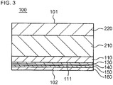
- FIG. 3 illustrates a layer structure which is more specific than that in FIG. 2 .
- FIG. 4 illustrates a state where the plate-like portion 100 is fixed to a fixation member 300.
- the light emitting element is a bottom emission type light emitting element, and emits light from the other surface 101 (the convex surface) side.
- the entire glass substrate 110 is positioned toward the one surface 102 side of the plate-like portion 100 than a center C3 of the thickness direction of the plate-like portion 100.
- the light emitting element according to this example is provided with the flexible plate-like portion 100 which includes the glass substrate 110, and an organic functional layer 140 (described later) including the light emitting layer and formed on the one surface side of the glass substrate 110, and the entire glass substrate 110 is positioned toward the one surface 102 side of the plate-like portion 100 than the center C3 of the thickness direction of the plate-like portion 100.
- the entire glass substrate 110 is positioned toward the one surface 102 side of the plate-like portion 100 than the center surface C1 (refer to FIG. 1 ).
- the entire glass substrate 110 in a state where the plate-like portion 100 is curved, it is possible to obtain a state where a compressive stress is generated in the entire glass substrate 110.
- the light emitting element includes the glass substrate 110, a first electrode 130, the organic functional layer 140, and a second electrode 150.
- the organic functional layer 140 is arranged between the first electrode 130 and the second electrode 150.
- the first electrode 130 is arranged between the organic functional layer 140 and the glass substrate 110.
- the first electrode 130 for example, is a transparent electrode formed of a metal oxide conductor of Indium Tin Oxide (ITO), Indium Zinc Oxide (IZO), and the like.
- the first electrode 130 may be a thin metal film which is thin to the extent of transmitting light.
- the second electrode 150 for example, is a reflective electrode formed of a metal layer of Ag, Au, Al, and the like.
- the second electrode 150 reflects light which is directed towards the second electrode 150 side from the organic functional layer 140.
- the second electrode 150 may be a transparent electrode formed of a metal oxide conductor of ITO, IZO, and the like, and a light reflective layer (not illustrated) may be disposed below the second electrode 150.
- the thickness of a metal layer configuring the second electrode 150 may be thin to have light transmissivity, and thus may function as a transparent light emitting element at the time of not emitting light.
- Any one of the first electrode 130 and the second electrode 150 is an anode, and the other is a cathode.
- a work function of a material configuring the cathode is different from a work function of a material configuring the anode.
- one surface of the glass substrate 110 (a lower surface in FIG. 4 ) and one surface of the first electrode 130 (an upper surface in FIG. 1 ) are in contact with each other.
- the other surface of the first electrode 130 (a lower surface in FIG. 1 ) and one surface of the organic functional layer 140 (an upper surface in FIG. 1 ) are in contact with each other.
- the other surface of the organic functional layer 140 (a lower surface in FIG. 1 ) and one surface of the second electrode 150 are in contact with each other.
- another layer may be disposed between the glass substrate 110 and the first electrode 130.
- another layer may be disposed between the first electrode 130 and the organic functional layer 140.
- another layer may be disposed between the organic functional layer 140 and the second electrode 150.
- the plate-like portion 100 further includes a resin layer 210 which is arranged toward the other surface 101 side of the plate-like portion 100 than the glass substrate 110.
- a layer thickness of the resin layer 210 is thicker than the thickness T of the glass substrate 110.
- the resin layer 210 is a light transmissive resin.
- the resin layer 210 for example, is formed of any one of polyethylene naphthalate (PEN), polyether sulfone (PES), polycarbonate (PC), polyethylene terephthalate (PET), polyimide, and polyamide.
- PEN polyethylene naphthalate
- PES polyether sulfone
- PC polycarbonate
- PET polyethylene terephthalate
- polyimide polyimide
- polyamide polyamide
- the resin layer 210 may have an organic and inorganic hybrid structure.
- the organic and inorganic hybrid structure a structure configured by impregnating glass fiber cloth with a resin is included.
- the resin layer 210 (referred to as a resin-containing layer) has light transmissivity.
- the resin layer 210 for example, is in contact with a surface of the glass substrate 110 on a side opposite to the first surface 111.
- another layer may be disposed between the glass substrate 110 and the resin layer 210.
- the plate-like portion 100 further includes a light extraction film 220 which is disposed on a side of the resin layer 210 opposite to the glass substrate 110 side.
- the light extraction film 220 for example, is formed of a microlens array sheet or a scattering sheet.
- the light extraction film 220 for example, is in contact with the side of the resin layer 210 opposite to the glass substrate 110 side.
- another layer may be disposed between the resin layer 210 and the light extraction film 220.
- the organic functional layer 140 is arranged toward the other surface 102 side of the plate-like portion 100 than the glass substrate 110.
- the plate-like portion 100 further includes a sealing layer 160.
- the sealing layer 160 covers the lower surface of the second electrode 150.
- the sealing layer 160 for example, is formed by sealing a layer formed of an inorganic solid (a SiON film, an Al 2 O 3 film, and the like) .
- the sealing layer 160 for example, may be formed by Chemical Vapor Deposition (CVD) or Atomic Layer Deposition (ALD).
- CVD Chemical Vapor Deposition
- ALD Atomic Layer Deposition
- a protective film formed of an organic material may be formed below an inorganic solid layer.
- solid sealing for example, attaching an aluminum foil by a thermosetting epoxy adhesive agent, or the like may be performed.
- the light emitting element further includes the fixation member 300 including a curved surface (for example, a concave surface 301).
- the plate-like portion 100 is fixed to the fixation member 300 along a concave curve of the fixation member 300, and is curved such that the one surface 102 of the plate-like portion 100 is a concave surface, and the other surface 101 thereof is a convex surface.
- the fixation member 300 has light transmissivity.
- the fixation member 300 for example, is formed of a transparent acrylic plate.
- a surface of the fixation member 300 on a side opposite to the concave surface 301 is a convex surface.
- the surface of the fixation member 300 on the side opposite to the concave surface 301 may be a flat surface, or may be a surface having another shape.
- a voltage is applied between the first electrode 130 and the second electrode 150, and thus the light emitting layer of the organic functional layer 140 emits light.
- All of the organic functional layer 140, the first electrode 130, the glass substrate 110, the resin layer 210 and the light extraction film 220, and the fixation member 300 transmit at least a part of the light emitted by the light emitting layer of the organic functional layer 140.
- a part of the light emitted by the light emitting layer is emitted to the outside of the light emitting element from the upper surface of the fixation member 300.
- FIG. 5 is a side cross-sectional view illustrating a first example of the layer structure of the organic functional layer 140.
- the organic functional layer 140 has a structure in which a hole injection layer 141, a hole transport layer 142, a light emitting layer 143, an electron transport layer 144, and an electron injection layer 145 are laminated in this order. That is, the organic functional layer 140 is an organic electroluminescent light emitting layer. Furthermore, instead of the hole injection layer 141 and the hole transport layer 142, one layer which functions as these two layers may be disposed. Similarly, instead of the electron transport layer 144 and the electron injection layer 145, one layer which functions as these two layers may be disposed.
- the light emitting layer 143 for example, is a layer emitting red light, a layer emitting blue light, or a layer emitting green light.
- a region including the light emitting layer 143 which emits red light, a region including the light emitting layer 143 which emits green light, and a region including the light emitting layer 143 which emits blue light may be repeatedly disposed.
- the light emitting element when the respective regions simultaneously emit light, the light emitting element emits light having a single color such as a white color.
- the light emitting layer 143 may be configured to emit light having a single color such as a white color by mixing materials for emitting light having a plurality of colors.
- FIG. 6 is a side cross-sectional view illustrating a second example of the layer structure of the organic functional layer 140.
- the light emitting layer 143 of the organic functional layer 140 has a configuration in which light emitting layers 143a, 143b, and 143c are laminated in this order.
- the light emitting layers 143a, 143b, and 143c emit light having colors different from each other (for example, red, green, and blue) . Then, when the light emitting layers 143a, 143b, and 143c simultaneously emit light, the light emitting element emits light having a single color such as a white color.
- a light transmissive conductive film formed of a metal oxide conductor of ITO, IZO, and the like is formed on the lower surface of the glass substrate 110 (the first surface 111) by a sputtering method or the like, and the light transmissive conductive film is patterned by etching, and thus the first electrode 130 is formed.
- an organic material is formed into a film on the lower surface of the first electrode 130, and thus the organic functional layer 140 is formed.
- a metal material such as Ag, Au, and Al is deposited in a desired pattern on the lower surface of the organic functional layer 140 by a vapor deposition method or the like, and thus the second electrode 150 is formed.
- the sealing layer 160 is formed on the lower surface of the second electrode 150.
- each of a bus line and a partition wall portion may be formed at a suitable timing.
- the bus line is configured of a material having resistance lower than that of the first electrode 130, and is disposed to be in contact with the first electrode 130.
- the partition wall portion partitions the organic functional layer 140 into a plurality of regions in a plan view and is configured of an insulating film.
- the entire glass substrate 110 is positioned toward the one surface 102 side of the plate-like portion 100 than the center C3 of the thickness direction of the plate-like portion 100, and thus, in a state where the plate-like portion 100 is curved, it is possible to expect that a compressive stress is generated in the entire glass substrate 110. Accordingly, it is possible to further suppress a breakage in the glass substrate 110.
- the plate-like portion 100 further includes the resin layer 210 which is arranged toward the other surface 101 side of the plate-like portion 100 than the glass substrate 110, and a layer thickness of the resin layer 210 is thicker than the thickness T of the glass substrate 110. Accordingly, it is possible to easily realize a configuration in which the entire glass substrate 110 is positioned toward the one surface 102 side than the center C3 of the thickness direction of the plate-like portion 100.
- the light emitting element further includes the fixation member 300 including the curved surface (for example, the concave surface 301), and the plate-like portion 100 is fixed to the fixation member 300 along the curved surface of the fixation member 300 and is bent such that the one surface 102 of the plate-like portion 100 is a concave surface, and the other surface 101 thereof is a convex surface. Accordingly, it is possible to constantly maintain the curving direction of the plate-like portion 100. Furthermore, the curving direction of the plate-like portion 100 is a direction in which a breakage in the glass substrate 110 is suppressed.
- the fixation member 300 including the curved surface (for example, the concave surface 301)
- the plate-like portion 100 is fixed to the fixation member 300 along the curved surface of the fixation member 300 and is bent such that the one surface 102 of the plate-like portion 100 is a concave surface, and the other surface 101 thereof is a convex surface. Accordingly, it is possible to constantly maintain the curving direction of the plate
- the curved surface of the fixation member 300 is the concave surface 301, and thus the plate-like portion 100 is pressed to the concave surface 301 of the fixation member 300 by an elastic force of the plate-like portion 100 trying to restore its flat shape. Accordingly, even when the plate-like portion 100 is not firmly fixed to the fixation member 300, the plate-like portion 100 easily maintains a state of being attached to the fixation member 300.
- a surface (a light emitting surface) on the light extraction film 220 side which is exposed to a user side is covered with the fixation member 300, and thus the light emitting element is able to have a structure which is resistant to impact from the outside.
- Example 1 an example is described in which the fixation member 300 is arranged only in the other surface 101 side of the plate-like portion 100.
- the plate-like portion 100 may be fixed by being interposed between a concave surface of a first fixation member including a concave surface and a convex surface of a second fixation member including a convex surface.
- the both surfaces of the plate-like portion 100 are able to be protected by the first fixation member and the second fixation member, respectively.
- a configuration of the plate-like portion 100 of the light emitting element according to this example is identical to that in Example 1 described above.
- a specific structure of the plate-like portion 100 will be described with reference to a distribution model of a stress in the glass substrate 110.
- FIG. 7 is a diagram for illustrating a stress generated in the plate-like portion 100 at the time of bending the plate-like portion 100.
- a distribution of the stress in the plate-like portion 100 is illustrated in a region R1
- a width (a width b) in a direction orthogonal to the thickness direction of each layer in the plate-like portion 100 is illustrated in a region R2
- Young's modulus (longitudinal elastic modulus) E of each layer in the plate-like portion 100 is illustrated in a region R3.
- a vertical axis is a thickness direction position y.
- a horizontal axis of the region R1 is the size of the stress
- a horizontal axis of the region R2 is the width b
- a horizontal axis of the region R3 is the Young's modulus E.
- the center surface C1 illustrated in FIG. 2 is a surface keeping a balance between a tensile stress and a compressive stress in a state where the plate-like portion 100 is curved.
- the width b of the organic functional layer 140 and the sealing layer 160 is slightly less than the width b of the glass substrate 110 which is nearly negligible, and thus the width b is able to be constant in an actual light emitting element.
- a stress ⁇ generated in the plate-like portion 100 is able to be calculated by Expression 2 described below.
- ⁇ is a curvature radius of the plate-like portion 100.
- the stress ⁇ is proportionate to the distance from the center surface C1 and the Young's modulus, and is inversely proportionate to the curvature radius ⁇ .
- a tensile stress TL is generated toward the convex surface side than on the center surface C1 in the plate-like portion 100, and a compressive stress CS is generated on the concave surface side.
- an example of the thickness of each layer in the plate-like portion 100 is as follows.
- the resin layer 210 is a substrate formed of PEN.
- the first electrode 130 is formed of ITO.
- the sealing layer 160 includes a CVD film of SiON, and a protective film formed of an ultraviolet curable resin.
- the position ⁇ of the center surface C1 is 76 ⁇ m according to Expression (3) described above.
- the position of the center C2 (refer to FIG. 1 ) of the thickness direction of the glass substrate 110 is 46 ⁇ m, and the center C2 is arranged on a position which is shifted to the one surface 102 (the concave surface) side from the position ⁇ of the center surface C1.
- the upper surface of the glass substrate 110 is also arranged on a position which is shifted to the one surface 102 (the concave surface) side from the position ⁇ of the center surface C1 by 21 ⁇ m. That is, in a state where the plate-like portion 100 is curved, the entire glass substrate 110 receives a compressive stress.
- a breakage (cracking) in the glass substrate 110 predominantly progresses due to a tensile stress, and the glass substrate 110 is rarely broken by a compressive stress.
- a portion of greater than or equal to one-half of the glass substrate 110 is able to receive a compressive stress.
- the plate-like portion 100 is bent at a high curvature, it is possible to suppress a breakage in the glass substrate 110.
- the entire glass substrate 110 is arranged in the position which is shifted to the concave surface side from the center surface C1, and the entire glass substrate 110 receives a compressive stress.
- the center C2 of the thickness direction of the glass substrate 110 (refer to FIG. 1 ) is shifted to the concave surface side from the center surface C1.
- the plate-like portion 100 when the plate-like portion 100 was curved in the direction of FIG. 2 , the plate-like portion 100 was able to be bent without being broken to a curvature of 1/3, compared to a case where the plate-like portion 100 was curved in the direction opposite to that of FIG. 2 .
- the reason for this may be that, although a tensile stress is applied on the convex surface side of the glass substrate 110 when the plate-like portion 100 is curved in any direction, as shown in Expression 2, the stress decreases as the distance from the center surface C1 becomes shorter.
- the tensile stress is further decreased when the plate-like portion 100 is curved in the direction shown in FIG. 2 , at the same curvature of the plate-like portion 100.
- FIG. 8 is a schematic side cross-sectional view of a light emitting element according to Example 3.
- the light emitting element is a bottom emission type light emitting element, and emits light from the other surface 101 (the convex surface) side.
- the light emitting element is a bottom emission type light emitting element, and emits light from the one surface 102 (the concave surface) side.
- the glass substrate 110, the first electrode 130, the organic functional layer 140, the second electrode 150, and the sealing layer 160 are arranged on the one surface 102 side on the basis of the resin layer 210 in this order.
- the sealing layer 160, the second electrode 150, the organic functional layer 140, the first electrode 130, the glass substrate 110, and the light extraction film 220 are arranged on the one surface 102 side on the basis of the resin layer 210 in this order.
- an upper surface of the resin layer 210 is the other surface 101
- a lower surface of the light extraction film 220 is the one surface 102.
- the light emitting element may also include the fixation member 300 described above.
- resin layer 210 has light transmissivity.
- the light emitting layer of the organic functional layer 140 emits light.
- the light from the light emitting layer is transmitted through the first electrode 130, the glass substrate 110, and the light extraction film 220 in this order, and is emitted to the outside of the light emitting element from the lower surface of the light extraction film 220.
- the light extraction film 220 is formed as thinly as possible. Alternatively, it is preferable to omit the light extraction film 220. In addition, it is preferable that a sealing solid having a thickness greater than that of a sealing film is used as the sealing layer 160.
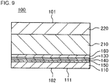
- FIG. 9 is a schematic side cross-sectional view of a light emitting element according to Example 4.
- the light emitting element is a bottom emission type light emitting element.
- the light emitting element is a top emission type light emitting element.
- light is emitted from the other surface 101 (the convex surface) side.
- the glass substrate 110, the first electrode 130, the organic functional layer 140, the second electrode 150, and the sealing layer 160 are arranged on the one surface 102 side on the basis of the resin layer 210 in this order.
- the sealing layer 160, the first electrode 130, the organic functional layer 140, the second electrode 150, and the glass substrate 110 are arranged on the one surface 102 side on the basis of the resin layer 210 in this order.
- the upper surface of the resin layer 210 is the other surface 101
- the lower surface of the glass substrate 110 is the one surface 102.
- the light emitting element may also include the fixation member 300 described above.
- the sealing layer 160 has light transmissivity.
- the light emitting layer of the organic functional layer 140 emits light.
- the light from the light emitting layer is transmitted through the first electrode 130, the sealing layer 160, the resin layer 210, and the light extraction film 220 in this order, and is emitted to the outside of the light emitting element from the upper surface of the light extraction film 220.
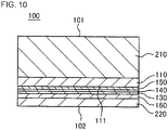
- FIG. 10 is a schematic side cross-sectional view of a light emitting element according to Example 5.
- the light emitting element is a bottom emission type light emitting element.
- the light emitting element is a top emission type light emitting element.
- the other surface 101 (the concave surface) side is a surface 101 (the concave surface) side.
- the glass substrate 110, the first electrode 130, the organic functional layer 140, the second electrode 150, and the sealing layer 160 are arranged on the one surface 102 side on the basis of the resin layer 210 in this order.
- the glass substrate 110, the second electrode 150, the organic functional layer 140, the first electrode 130, the sealing layer 160, and the light extraction film 220 are arranged on the one surface 102 side on the basis of the resin layer 210 in this order.
- the upper surface of the resin layer 210 is the other surface 101
- the lower surface of the light extraction film 220 is the one surface 102.
- the light emitting element may also include the fixation member 300 described above.
- the resin layer 210 has light transmissivity.
- the sealing layer 160 has light transmissivity.
- the light emitting layer of the organic functional layer 140 emits light.
- the light from the light emitting layer is transmitted through the first electrode 130, the sealing layer 160, and the light extraction film 220 in this order, and is emitted to the outside of the light emitting element from the lower surface of the light extraction film 220.
- the light extraction film 220 is formed as thinly as possible. Alternatively, it is preferable to omit the light extraction film 220. In addition, it is preferable that a sealing solid having a thickness greater than that of a sealing film is used as the sealing layer 160.
- FIG. 11 is a schematic exploded perspective view of a light emitting element according to Example 6.
- FIG. 12(a) is a schematic cross-sectional view of the light emitting element according to Example 6 (when the light emitting element is not curved)
- FIG. 12 (b) is a schematic cross-sectional view of the light emitting element according to Example 6 (when the light emitting element is curved)
- FIG. 12 (c) is a schematic side cross-sectional view of the light emitting element according to Example 6.
- the light emitting element according to this example is different from the light emitting element according to Example 1 described above in the following description, and the other configuration is identical to that of the light emitting element according to Example 1 described above.
- the plate-like portion 100 of the light emitting element according to this example has the same configuration as that of the plate-like portion 100 according to any one of Examples 1 to 5 described above.
- the light emitting element according to this example includes a fixation member 400 instead of the fixation member 300 described above ( FIG. 4 ).
- the fixation member 400 is able to be subjected to plastic deformation, and is fixed to the other surface 101 side of the plate-like portion 100 ( FIG. 12(a) ). Then, the plate-like portion 100 is curved along with the fixation member 400, and thus the other surface 101 of the plate-like portion 100 is a convex surface, and the one surface 102 thereof is a concave surface, and thus the plate-like portion 100 is maintained in a curved state by the fixation member 400 ( FIG. 12(b) and FIG. 12(c) ).
- the fixation member 400 is subjected to the plastic deformation, and thus the fixation member 400 is maintained in the shape after the plastic deformation.
- the flexible plate-like portion 100 is restrained by the fixation member 400, and thus the plate-like portion 100 is maintained in a bent state by the fixation member 400.
- the fixation member 400 is curved along with the plate-like portion 100, and thus the fixation member 400 is subjected to the plastic deformation into the shape which includes a curved surface.
- the plate-like portion 100 is in the shape of a rectangle.
- the fixation member 400 is formed in the shape of a rectangular frame of the plate-like portion 100.
- the fixation member 400 includes four linear plate-like portions 401 to 404 which extend along each side of the plate-like portion 100. Among them, the plate-like portion 401 and the plate-like portion 403 face each other and are in parallel, and the plate-like portion 402 and the plate-like portion 404 face each other and are in parallel. In addition, the plate-like portions 402 and 403 are orthogonal to the plate-like portions 401 and 403. A rectangular opening portion 400a is formed in center portion of the fixation member 400.
- the plate-like portions 401 and 403 are curved into the shape of an arc, and the plate-like portion 100 is curved, and thus the plate-like portions 401 and 403 are subjected to the plastic deformation, and the plate-like portion 100 is maintained in a curved state.
- the fixation member 400 includes a first portion (the plate-like portion 401) which extends along a first side of the plate-like portion 100, and a second portion (the plate-like portion 402) which extends along a second side facing the first side of the plate-like portion 100. Then, each of the first portion and the second portion is curved into the shape of an arc.
- the plate-like portion 100 has the configuration according to any one of Examples 1 to 5 described above, it is possible to preferably release heat through the opening portion 400a of the fixation member 400.
- the fixation member 400 for example, is able to be configured of metal.
- a method of fixing the plate-like portion 100 to the fixation member 400 is not limited, and for example, the plate-like portion 100 is able to be fixed to the fixation member 400 by using an adhesive agent.
- the same effect (excluding the effect which is able to be obtained by the fixation member 300) as that of Example 1 described above is able to be obtained, and the following effect is able to be obtained.
- the fixation member 400 is curved along with the plate-like portion 100, and thus the fixation member 400 is subjected to the plastic deformation into the shape including the curved surface. Accordingly, the plate-like portion 100 is maintained in a curved state in which the one surface 102 of the plate-like portion 100 is a concave surface, and the other surface 101 thereof is a convex surface, by the fixation member 400. That is, the curving direction of the plate-like portion 100 is able to be constantly maintained by the fixation member 400. Furthermore, the bending direction of the plate-like portion 100 is a direction in which a breakage in the glass substrate 110 is suppressed.
- the entire light emitting element composed of the fixation member 400 and the plate-like portion 100 joined together is curved, and thus the same effect as that of moving the center surface C1 described above to the fixation member 400 side (an upper side in FIGS. 12(b) and 12(c) ) is able to be obtained, compared to Example 1.
- Example 1 the same effect as that of increasing the layer thickness of the resin layer 210 is able to be obtained.
- the plate-like portion 100 is in the shape of a rectangle
- the fixation member 400 includes the first portion (the plate-like portion 401) which extends along the first side of the plate-like portion 100 and the second portion (the plate-like portion 402) which extends along the second side facing the first side of the plate-like portion 100. Then, each of the first portion and the second portion is curved into the shape of an arc. Therefore, the plate-like portion 100 is maintained in a curved state in which the one surface 102 of the plate-like portion 100 is a concave surface, and the other surface 101 thereof is a convex surface, by the fixation member 400.
- a compressive stress may also be generated in the glass substrate 110 by performing a chemical treatment with respect to the glass substrate 110.
Description
- The present invention relates to a light emitting element.
- As light emitting elements, there is one including an organic light emitting layer, that is, an organic Electro Luminescence (EL) element. There is a type of the organic EL element which is flexible, that is, an organic EL element which has flexibility and is able to be bent (
Patent Documents 1 to 5). There is one type of such a flexible organic EL element of which a base material includes a glass substrate (Patent Documents 1 and 2). The glass substrate is able to prevent moisture or oxygen from being transmitted, compared to a resin layer. - Furthermore, Patent Document 3 discloses a technology in which an inorganic moisture-proof layer is arranged approximately in a center portion in a thickness direction of the organic EL element, thus reducing a stress generated in the inorganic moisture-proof layer. Similarly, Patent Document 4 discloses a technology in which a gas barrier layer formed of silicon oxide, silicon oxynitride, and the like is arranged in the vicinity of a position which is a neutral surface at the time of bending the organic EL element, and thus the generation of the stress in the gas barrier layer is reduced. Similarly, Patent Document 5 discloses a technology in which an inorganic insulating film formed of a silicon oxynitride film or the like is arranged in the vicinity of a neutral axis at the time of applying a bending stress to the organic EL element.
- Patent Document 6 discloses a flexible display device having an insulating substrate which has withstood a high temperature process and is reliable even in mechanical strength.
- Patent Document 7 discloses flexible devices including semiconductor nanocrystals, arrays including such devices, systems including the foregoing, and related methods.
- Patent Document 8 discloses a transparent or substantially transparent formable and/or flexible component for use as an outer protective element in an electronic or opto electronic device including at least one electrically active organic layer.
- Patent document 9 discloses an EL element capable of preventing respective layers that form the EL element from being broken when the EL element is curved.
-
- [Patent Document 1]
JP 2003-337549 A - [Patent Document 2]
JP 2007-10834 A - [Patent Document 3]
JP 2003-168556 A - [Patent Document 4]
JP 2005-251671 A - [Patent Document 5]
WO 2005/027582 A1 - [Patent Document 6]
JP 2006-221892 A - [Patent Document 7]
WO 2009/099425 A2 - [Patent Document 8]
GB 2 335 884 A - [Patent Document 9]
JP 2009-170173 A -
EP2259321 discloses a flexible OLED element wherein the neutral plane is positioned in the plane of sensitive elements. - The glass substrate may easily crack when bent due to properties thereof. For this reason, it is desirable to suppress the cracking of the glass substrate.
- An example of an object of the present invention is to suppress cracking of a glass substrate included in a light emitting element.
- The invention is a light emitting element according to
claim 1. - The object described above, and other objects, characteristics, and advantages will become more obvious with reference to the following preferred embodiments and the following drawings attached thereto.
-
-
FIG. 1 is a schematic side cross-sectional view of a light emitting element according to an embodiment used to illustrate the principle of the present invention. -
FIG. 2 is a schematic side cross-sectional view of a light emitting element according to Example 1. -
FIG. 3 is a schematic side cross-sectional view of the light emitting element according to Example 1. -
FIG. 4 is a schematic side cross-sectional view of the light emitting element according to Example 1. -
FIG. 5 is a side cross-sectional view illustrating a first example of a layer structure of an organic functional layer. -
FIG. 6 is a side cross-sectional view illustrating a second example of the layer structure of the organic functional layer. -
FIG. 7 is a diagram for illustrating a stress generated in a plate-like portion when the plate-like portion is bent. -
FIG. 8 is a schematic side cross-sectional view of a light emitting element according to Example 3. -
FIG. 9 is a schematic side cross-sectional view of a light emitting element according to Example 4. -
FIG. 10 is a schematic side cross-sectional view of a light emitting element according to Example 5. -
FIG. 11 is a schematic exploded perspective view of a light emitting element according to Example 6. -
FIG. 12(a) is a schematic cross-sectional view of the light emitting element according to Example 6 (when the light emitting element is not bent),FIG. 12(b) is a schematic cross-sectional view of the light emitting element according to Example 6 (when the light emitting element is bent), andFIG. 12(c) is a schematic side cross-sectional view of the light emitting element according to Example 6. - Hereinafter, embodiments of the present invention will be described with reference to the drawings. Furthermore, in all of the drawings, the same reference numerals are applied to the same constituent parts, and the descriptions thereof will not be repeated.
-
FIG. 1 is a side cross-sectional view of a light emitting element according to an embodiment used to illustrate the principle of the present invention. The light emitting element includes a flexible plate-like portion 100. The plate-like portion 100 includes aglass substrate 110, and an organic functional layer which is formed on one surface side of theglass substrate 110. The organic functional layer includes a light emitting layer. The configuration of the organic functional layer will be described later in examples. When the plate-like portion 100 is curved in a prescribed curving direction, and thus onesurface 102 of the plate-like portion 100 is a concave surface, and theother surface 101 thereof is a convex surface, a surface positioned on the concave surface side among both surfaces of theglass substrate 110 is referred to as afirst surface 111. In addition, the thickness of theglass substrate 110 is T. When the plate-like portion 100 is curved in a prescribed curving direction, and thus the onesurface 102 of the plate-like portion 100 is a concave surface, and theother surface 101 thereof is a convex surface, a compressive stress is applied to a portion (a compressivestress generation portion 112 inFIG. 1 ) whose distance from thefirst surface 111 of theglass substrate 110 is less than or equal to L (L > T/2). - Furthermore, as described later, for the sake of simple description, a positional relationship (an up and down relationship or the like) of each constituent of the light emitting element will be described by using a relationship illustrated in each drawing. However, the positional relationship in the description has no connection to a positional relationship at the time of using the light emitting element or at the time of manufacturing the light emitting element.
- In addition, in the following description, an operation in which the plate-
like portion 100 is curved in a prescribed curving direction, and thus the onesurface 102 of the plate-like portion 100 is a concave surface, and theother surface 101 thereof is a convex surface, is simply referred to as an operation of curving the plate-like portion 100. - The
glass substrate 110 is formed of light transmissive glass. Theglass substrate 110 is formed to have a thickness to the extent of having flexibility. It is preferable that the thickness of theglass substrate 110, for example, is approximately greater than or equal to 10 µm and less than or equal to 200 µm. - When the
glass substrate 110 is formed to have a thickness of less than or equal to a certain degree of thickness, a certain degree of flexibility is able to be obtained. However, even when theglass substrate 110 is formed to be sufficiently thin, theglass substrate 110 cracks beginning at a trivial breakage point when theglass substrate 110 is bent at a large curvature exceeding the limitation (at a small curvature radius). - The present inventors have investigated a breakage (cracking) in the
glass substrate 110, and thus have found that a crack predominantly progresses due to a tensile stress, and theglass substrate 110 is rarely broken by a compressive stress. Accordingly, breakage (cracking) in theglass substrate 110 is suppressed by predetermining a bending (curving) direction of the plate-like portion 100, and setting the arrangement of theglass substrate 110 in a thickness direction of the plate-like portion 100 such that a compressive stress is generated in a region with a thickness of greater than one-half of a thickness T of theglass substrate 110 in the thickness direction of theglass substrate 110 in a state where the plate-like portion 100 is curved. - When the plate-
like portion 100 is curved, a tensile stress is generated in a portion of the convex surface side (theother surface 101 side) of the plate-like portion 100, and a compressive stress is generated in a portion of the concave surface side (the onesurface 102 side). A center surface C1 illustrated inFIG. 1 is a surface keeping a balance between the tensile stress and the compressive stress in a state where the plate-like portion 100 is curved. - As described above, in a state where the plate-
like portion 100 is curved, a surface which is the concave surface side of the plate-like portion 100 among the both surfaces of theglass substrate 110 is referred to as thefirst surface 111. In a state where the plate-like portion 100 is curved, a compressive stress is applied to the compressivestress generation portion 112 which is a portion whose distance from thefirst surface 111 of theglass substrate 110 is less than or equal to L. L is greater than one-half of the thickness T of the glass substrate. That is, L > T/2. - In other words, in the thickness direction of the
glass substrate 110, a region with a thickness of greater than one-half of the thickness T of theglass substrate 110 is positioned on theother surface 101 side from the center surface C1. Accordingly, in a state where the plate-like portion 100 is curved, a compressive stress is generated in a region with a thickness of greater than one-half of the thickness T of theglass substrate 110, in the thickness direction of theglass substrate 110. - In addition, in the light emitting element according to this embodiment, a center C2 of the thickness direction of the glass substrate 110 (the center C2 of the
glass substrate 110 in the thickness direction of the glass substrate 110) is positioned toward the onesurface 102 side of the plate-like portion 100 than the center of the thickness direction of the plate-like portion 100 (the center of the plate-like portion 100 in the thickness direction of the plate-like portion 100: not illustrated). Furthermore, the center of the thickness direction of the plate-like portion 100 may be coincident with the center surface C1 described above, or may not be coincident with the center surface C1 described above. - The light emitting element according to this embodiment does not include a glass substrate (a glass substrate other than the glass substrate 110) at least toward the
other surface 101 side than theglass substrate 110. It is preferable that the glass substrate included in the light emitting element is only theglass substrate 110. - As described above, according to this embodiment, the light emitting element is provided with the flexible plate-
like portion 100 which includes theglass substrate 110, and the organic functional layer including the light emitting layer and formed on the one surface side of theglass substrate 110. When the plate-like portion 100 is curved in a prescribed curving direction, and thus the onesurface 102 of the plate-like portion 100 is a concave surface, and theother surface 101 thereof is a convex surface, the surface positioned on the concave surface side among the both surfaces of theglass substrate 110 is referred to as thefirst surface 111. In addition, the thickness of theglass substrate 110 is T. When the plate-like portion 100 is curved, a compressive stress is applied to the portion whose distance from thefirst surface 111 of theglass substrate 110 is less than or equal to L (L > T/2). That is, the arrangement of theglass substrate 110 in the thickness direction of the light emitting element is set such that the compressive stress is applied to the compressivestress generation portion 112 which is the portion whose distance from thefirst surface 111 of theglass substrate 110 is less than or equal to L. Accordingly, it is possible to suppress a breakage (cracking) in theglass substrate 110, and thus it is possible to improve flexibility and reliability of the plate-like portion 100 of the light emitting element. - Here, as described above, Patent Documents 3 to 5 disclose a technology in which the inorganic moisture-proof layer or the like is arranged approximately in the center portion in the thickness direction of the light emitting element, and thus a stress generated in the inorganic moisture-proof layer or the like is reduced. For this reason, even when the light emitting element is bent in any direction, the same stress is generated in the inorganic moisture-proof layer or the like. The inorganic moisture-proof film is an extremely thin film having a thickness which is usually less than or equal to 1 µm, and thus it is possible to significantly reduce the stress generated in the inorganic moisture-proof film by the configuration as in Patent Documents 3 to 5. However, even a
thin glass substrate 110, for example, has a thickness of greater than or equal to 10 µm, and thus when the center surface C1 is coincident with the center C2 of the thickness direction of theglass substrate 110, a tensile stress is generated in theglass substrate 110 when the plate-like portion 100 is bent in any direction. A microcrack, a chipping of an end surface, or the like frequently occurs in theglass substrate 110, and theglass substrate 110 is weak to tensile stress compared to the inorganic moisture-proof film, and thus, in a configuration in which theglass substrate 110 is arranged in the same position as that of the inorganic moisture-proof layer or the like as in Patent Documents 3 to 5, it is difficult to obtain a practically sufficient curvature radius and breakage resistance. - In contrast, in this embodiment, the curving direction of the light emitting element is prescribed to one direction, and the arrangement of the
glass substrate 110 in the thickness direction of the light emitting element is set such that the compressive stress is applied to the portion whose distance from thefirst surface 111 of theglass substrate 110 is less than or equal to L (L > T/2) at the time of bending the plate-like portion 100. Accordingly, it is possible to considerably reduce a tensile stress generated in theglass substrate 110. Alternatively, it is possible to obtain a state where only a compressive stress is generated in theglass substrate 110. As a result thereof, it is possible to bend the plate-like portion 100 at a smaller curvature radius, and it is possible to improve breakage resistance of theglass substrate 110. - Similarly, the center C2 of the thickness direction of the
glass substrate 110 is positioned toward the onesurface 102 side than the plate-like portion 100 from the center of the thickness direction of the plate-like portion 100, and thus a configuration is easily realized in which a compressive stress is applied to the compressivestress generation portion 112 which is the portion whose distance from thefirst surface 111 of theglass substrate 110 is less than or equal to L, and it is possible to suppress a breakage (cracking) in theglass substrate 110. - A light emitting element according to this example is different from the light emitting element according to embodiment described above in the following description, and the other configuration is identical to that of the light emitting element according to embodiment described above.
- Each drawing of
FIG. 2 to FIG. 4 is a schematic side cross-sectional view of the light emitting element according to this example. Among them,FIG. 2 illustrates a schematic configuration of the plate-like portion 100.FIG. 3 illustrates a layer structure which is more specific than that inFIG. 2 .FIG. 4 illustrates a state where the plate-like portion 100 is fixed to afixation member 300. - In this example, an example will be described in which the light emitting element is a bottom emission type light emitting element, and emits light from the other surface 101 (the convex surface) side.
- As illustrated in
FIG. 2 , in this example, theentire glass substrate 110 is positioned toward the onesurface 102 side of the plate-like portion 100 than a center C3 of the thickness direction of the plate-like portion 100. - That is, the light emitting element according to this example is provided with the flexible plate-
like portion 100 which includes theglass substrate 110, and an organic functional layer 140 (described later) including the light emitting layer and formed on the one surface side of theglass substrate 110, and theentire glass substrate 110 is positioned toward the onesurface 102 side of the plate-like portion 100 than the center C3 of the thickness direction of the plate-like portion 100. - Accordingly, as illustrated in
FIG. 2 , in a state where the plate-like portion 100 is curved, it is possible to expect that a compressive stress is generated in theentire glass substrate 110. - Furthermore, it is preferable that the
entire glass substrate 110 is positioned toward the onesurface 102 side of the plate-like portion 100 than the center surface C1 (refer toFIG. 1 ). Thus, as illustrated inFIG. 2 , in a state where the plate-like portion 100 is curved, it is possible to obtain a state where a compressive stress is generated in theentire glass substrate 110. - As illustrated in
FIG. 3 , the light emitting element includes theglass substrate 110, afirst electrode 130, the organicfunctional layer 140, and asecond electrode 150. The organicfunctional layer 140 is arranged between thefirst electrode 130 and thesecond electrode 150. Thefirst electrode 130 is arranged between the organicfunctional layer 140 and theglass substrate 110. - The
first electrode 130, for example, is a transparent electrode formed of a metal oxide conductor of Indium Tin Oxide (ITO), Indium Zinc Oxide (IZO), and the like. However, thefirst electrode 130 may be a thin metal film which is thin to the extent of transmitting light. - The
second electrode 150, for example, is a reflective electrode formed of a metal layer of Ag, Au, Al, and the like. Thesecond electrode 150 reflects light which is directed towards thesecond electrode 150 side from the organicfunctional layer 140. However, thesecond electrode 150 may be a transparent electrode formed of a metal oxide conductor of ITO, IZO, and the like, and a light reflective layer (not illustrated) may be disposed below thesecond electrode 150. Alternatively, the thickness of a metal layer configuring thesecond electrode 150 may be thin to have light transmissivity, and thus may function as a transparent light emitting element at the time of not emitting light. - Any one of the
first electrode 130 and thesecond electrode 150 is an anode, and the other is a cathode. A work function of a material configuring the cathode is different from a work function of a material configuring the anode. - For example, one surface of the glass substrate 110 (a lower surface in
FIG. 4 ) and one surface of the first electrode 130 (an upper surface inFIG. 1 ) are in contact with each other. In addition, the other surface of the first electrode 130 (a lower surface inFIG. 1 ) and one surface of the organic functional layer 140 (an upper surface inFIG. 1 ) are in contact with each other. In addition, the other surface of the organic functional layer 140 (a lower surface inFIG. 1 ) and one surface of the second electrode 150 (an upper surface inFIG. 1 ) are in contact with each other. However, another layer may be disposed between theglass substrate 110 and thefirst electrode 130. Similarly, another layer may be disposed between thefirst electrode 130 and the organicfunctional layer 140. Similarly, another layer may be disposed between the organicfunctional layer 140 and thesecond electrode 150. - The plate-
like portion 100 further includes aresin layer 210 which is arranged toward theother surface 101 side of the plate-like portion 100 than theglass substrate 110. A layer thickness of theresin layer 210 is thicker than the thickness T of theglass substrate 110. - The
resin layer 210, for example, is a light transmissive resin. Theresin layer 210, for example, is formed of any one of polyethylene naphthalate (PEN), polyether sulfone (PES), polycarbonate (PC), polyethylene terephthalate (PET), polyimide, and polyamide. - Furthermore, the
resin layer 210 may have an organic and inorganic hybrid structure. As the organic and inorganic hybrid structure, a structure configured by impregnating glass fiber cloth with a resin is included. In this case, the resin layer 210 (referred to as a resin-containing layer) has light transmissivity. - The
resin layer 210, for example, is in contact with a surface of theglass substrate 110 on a side opposite to thefirst surface 111. However, another layer may be disposed between theglass substrate 110 and theresin layer 210. - The plate-
like portion 100 further includes alight extraction film 220 which is disposed on a side of theresin layer 210 opposite to theglass substrate 110 side. Thelight extraction film 220, for example, is formed of a microlens array sheet or a scattering sheet. Thelight extraction film 220, for example, is in contact with the side of theresin layer 210 opposite to theglass substrate 110 side. However, another layer may be disposed between theresin layer 210 and thelight extraction film 220. - The organic
functional layer 140 is arranged toward theother surface 102 side of the plate-like portion 100 than theglass substrate 110. - The plate-
like portion 100 further includes asealing layer 160. Thesealing layer 160 covers the lower surface of thesecond electrode 150. Thesealing layer 160, for example, is formed by sealing a layer formed of an inorganic solid (a SiON film, an Al2O3 film, and the like) . Thesealing layer 160, for example, may be formed by Chemical Vapor Deposition (CVD) or Atomic Layer Deposition (ALD). Furthermore, a protective film formed of an organic material may be formed below an inorganic solid layer. Further, solid sealing (for example, attaching an aluminum foil by a thermosetting epoxy adhesive agent, or the like) may be performed. - As illustrated in
FIG. 4 , the light emitting element according to this example further includes thefixation member 300 including a curved surface (for example, a concave surface 301). The plate-like portion 100 is fixed to thefixation member 300 along a concave curve of thefixation member 300, and is curved such that the onesurface 102 of the plate-like portion 100 is a concave surface, and theother surface 101 thereof is a convex surface. - In this example, the
fixation member 300 has light transmissivity. Thefixation member 300, for example, is formed of a transparent acrylic plate. - Furthermore, a surface of the
fixation member 300 on a side opposite to the concave surface 301 (an upper surface inFIG. 4 ), for example, is a convex surface. However, the surface of thefixation member 300 on the side opposite to theconcave surface 301 may be a flat surface, or may be a surface having another shape. - A voltage is applied between the
first electrode 130 and thesecond electrode 150, and thus the light emitting layer of the organicfunctional layer 140 emits light. All of the organicfunctional layer 140, thefirst electrode 130, theglass substrate 110, theresin layer 210 and thelight extraction film 220, and thefixation member 300 transmit at least a part of the light emitted by the light emitting layer of the organicfunctional layer 140. A part of the light emitted by the light emitting layer is emitted to the outside of the light emitting element from the upper surface of thefixation member 300. - Next, an example of a layer structure of the organic
functional layer 140 will be described. -
FIG. 5 is a side cross-sectional view illustrating a first example of the layer structure of the organicfunctional layer 140. The organicfunctional layer 140 has a structure in which ahole injection layer 141, ahole transport layer 142, alight emitting layer 143, anelectron transport layer 144, and anelectron injection layer 145 are laminated in this order. That is, the organicfunctional layer 140 is an organic electroluminescent light emitting layer. Furthermore, instead of thehole injection layer 141 and thehole transport layer 142, one layer which functions as these two layers may be disposed. Similarly, instead of theelectron transport layer 144 and theelectron injection layer 145, one layer which functions as these two layers may be disposed. - In this example, the
light emitting layer 143, for example, is a layer emitting red light, a layer emitting blue light, or a layer emitting green light. In this case, in a plan view, a region including thelight emitting layer 143 which emits red light, a region including thelight emitting layer 143 which emits green light, and a region including thelight emitting layer 143 which emits blue light may be repeatedly disposed. In this case, when the respective regions simultaneously emit light, the light emitting element emits light having a single color such as a white color. - Furthermore, the
light emitting layer 143 may be configured to emit light having a single color such as a white color by mixing materials for emitting light having a plurality of colors. -
FIG. 6 is a side cross-sectional view illustrating a second example of the layer structure of the organicfunctional layer 140. Thelight emitting layer 143 of the organicfunctional layer 140 has a configuration in which light emittinglayers light emitting layers light emitting layers - Next, an example of a manufacturing method of the light emitting element according to this embodiment will be described.
- First, a light transmissive conductive film formed of a metal oxide conductor of ITO, IZO, and the like is formed on the lower surface of the glass substrate 110 (the first surface 111) by a sputtering method or the like, and the light transmissive conductive film is patterned by etching, and thus the
first electrode 130 is formed. - Next, an organic material is formed into a film on the lower surface of the
first electrode 130, and thus the organicfunctional layer 140 is formed. - Next, a metal material such as Ag, Au, and Al is deposited in a desired pattern on the lower surface of the organic
functional layer 140 by a vapor deposition method or the like, and thus thesecond electrode 150 is formed. - Next, the
sealing layer 160 is formed on the lower surface of thesecond electrode 150. - Furthermore, as necessary, each of a bus line and a partition wall portion may be formed at a suitable timing. The bus line is configured of a material having resistance lower than that of the
first electrode 130, and is disposed to be in contact with thefirst electrode 130. The partition wall portion partitions the organicfunctional layer 140 into a plurality of regions in a plan view and is configured of an insulating film. - According to this example, the same effect as that in the embodiment described above is able to be obtained, and the following effect is able to be obtained.
- The
entire glass substrate 110 is positioned toward the onesurface 102 side of the plate-like portion 100 than the center C3 of the thickness direction of the plate-like portion 100, and thus, in a state where the plate-like portion 100 is curved, it is possible to expect that a compressive stress is generated in theentire glass substrate 110. Accordingly, it is possible to further suppress a breakage in theglass substrate 110. - The plate-
like portion 100 further includes theresin layer 210 which is arranged toward theother surface 101 side of the plate-like portion 100 than theglass substrate 110, and a layer thickness of theresin layer 210 is thicker than the thickness T of theglass substrate 110. Accordingly, it is possible to easily realize a configuration in which theentire glass substrate 110 is positioned toward the onesurface 102 side than the center C3 of the thickness direction of the plate-like portion 100. - The light emitting element further includes the
fixation member 300 including the curved surface (for example, the concave surface 301), and the plate-like portion 100 is fixed to thefixation member 300 along the curved surface of thefixation member 300 and is bent such that the onesurface 102 of the plate-like portion 100 is a concave surface, and theother surface 101 thereof is a convex surface. Accordingly, it is possible to constantly maintain the curving direction of the plate-like portion 100. Furthermore, the curving direction of the plate-like portion 100 is a direction in which a breakage in theglass substrate 110 is suppressed. - In addition, the curved surface of the
fixation member 300 is theconcave surface 301, and thus the plate-like portion 100 is pressed to theconcave surface 301 of thefixation member 300 by an elastic force of the plate-like portion 100 trying to restore its flat shape. Accordingly, even when the plate-like portion 100 is not firmly fixed to thefixation member 300, the plate-like portion 100 easily maintains a state of being attached to thefixation member 300. In addition, a surface (a light emitting surface) on thelight extraction film 220 side which is exposed to a user side is covered with thefixation member 300, and thus the light emitting element is able to have a structure which is resistant to impact from the outside. - Furthermore, in Example 1 described above, an example is described in which the
fixation member 300 is arranged only in theother surface 101 side of the plate-like portion 100. However, the plate-like portion 100 may be fixed by being interposed between a concave surface of a first fixation member including a concave surface and a convex surface of a second fixation member including a convex surface. In this case, the both surfaces of the plate-like portion 100 are able to be protected by the first fixation member and the second fixation member, respectively. - A configuration of the plate-
like portion 100 of the light emitting element according to this example is identical to that in Example 1 described above. In this example, a specific structure of the plate-like portion 100 will be described with reference to a distribution model of a stress in theglass substrate 110. -
FIG. 7 is a diagram for illustrating a stress generated in the plate-like portion 100 at the time of bending the plate-like portion 100. InFIG. 7 , a distribution of the stress in the plate-like portion 100 is illustrated in a region R1, a width (a width b) in a direction orthogonal to the thickness direction of each layer in the plate-like portion 100 is illustrated in a region R2, and Young's modulus (longitudinal elastic modulus) E of each layer in the plate-like portion 100 is illustrated in a region R3. In each of the regions R1 to R3, a vertical axis is a thickness direction position y. A horizontal axis of the region R1 is the size of the stress, a horizontal axis of the region R2 is the width b, and a horizontal axis of the region R3 is the Young's modulus E. - Here, the center surface C1 illustrated in
FIG. 2 is a surface keeping a balance between a tensile stress and a compressive stress in a state where the plate-like portion 100 is curved. - The width b and the Young's modulus E are functions of the position y in the thickness direction of the light emitting element, and when the light emitting element is in a position of y = 0 to y = h (that is, when the thickness of the light emitting element is h), a position λ of the center surface C1 in the thickness direction of the light emitting element is able to be calculated by
Expression 1 described below. - [Expression 1]

- The width b of the organic
functional layer 140 and thesealing layer 160 is slightly less than the width b of theglass substrate 110 which is nearly negligible, and thus the width b is able to be constant in an actual light emitting element. - In a state where the plate-
like portion 100 is bent at a constant curvature, a stress σ generated in the plate-like portion 100 is able to be calculated by Expression 2 described below. In Expression 2, ρ is a curvature radius of the plate-like portion 100. - [Expression 2]

- As in Expression 2 described above, the stress σ is proportionate to the distance from the center surface C1 and the Young's modulus, and is inversely proportionate to the curvature radius ρ.
- Here, as illustrated in the region R1 of
FIG. 7 , a tensile stress TL is generated toward the convex surface side than on the center surface C1 in the plate-like portion 100, and a compressive stress CS is generated on the concave surface side. - The position λ of the center surface C1 when the light emitting element is configured of three layers is able to be calculated by Expression 3 described below.
- [Expression 3]

- Here, an example of the thickness of each layer in the plate-
like portion 100 is as follows. - Thickness t1 of a portion including the
first electrode 130, the organicfunctional layer 140, thesecond electrode 150, and thesealing layer 160 = 5 µm - Thickness t2 of the
glass substrate 110 = 50 µm - Thickness t3 of the
resin layer 210 = 200 µm - Thickness t4 of the
light extraction film 220 = 100 µm - In addition, an example of the Young's modulus of each layer in the plate-
like portion 100 is as follows. - Young's modulus E1 of the portion including the
first electrode 130, the organicfunctional layer 140, thesecond electrode 150, and thesealing layer 160 = 3 GPa - Young's modulus E2 of the
glass substrate 110 = 70 GPa - Young's modulus E3 of the
resin layer 210 = 6 GPa - Young's modulus E4 of the
light extraction film 220 = 3 GPa - Furthermore, the
resin layer 210 is a substrate formed of PEN. Thefirst electrode 130 is formed of ITO. Thesealing layer 160 includes a CVD film of SiON, and a protective film formed of an ultraviolet curable resin. - In such conditions, the position λ of the center surface C1 is 76 µm according to Expression (3) described above. In addition, the position of the center C2 (refer to
FIG. 1 ) of the thickness direction of theglass substrate 110 is 46 µm, and the center C2 is arranged on a position which is shifted to the one surface 102 (the concave surface) side from the position λ of the center surface C1. In addition, the upper surface of theglass substrate 110 is also arranged on a position which is shifted to the one surface 102 (the concave surface) side from the position λ of the center surface C1 by 21 µm. That is, in a state where the plate-like portion 100 is curved, theentire glass substrate 110 receives a compressive stress. - Here, as it is known from the consideration of the present inventors, a breakage (cracking) in the
glass substrate 110 predominantly progresses due to a tensile stress, and theglass substrate 110 is rarely broken by a compressive stress. - When the plate-
like portion 100 of the light emitting element of this example was curved in a direction (a direction in which thesealing layer 160 side is a convex surface) opposite to that ofFIG. 2 , a crack occurred in theglass substrate 110 at the stage of ϕ80 mm (a curvature radius of 40 mm). In contrast, when the plate-like portion 100 of the light emitting element of this example is curved in the direction ofFIG. 2 , that is, a prescribed curving direction, no occurrence of cracking in theglass substrate 110 was confirmed even at ϕ10 mm (a curvature radius of 5 mm) . - Thus, by limiting the bending direction of the plate-
like portion 100 to one direction, and arranging theglass substrate 110 to be shifted toward the one surface 102 (the concave surface) side from the center surface C1, a portion of greater than or equal to one-half of theglass substrate 110 is able to receive a compressive stress. As a result thereof, even when the plate-like portion 100 is bent at a high curvature, it is possible to suppress a breakage in theglass substrate 110. - According to this example, the same effect as that of Example 1 described above is able to be obtained.
- Furthermore, when the light emitting surface side is bent to be convex as in this example and Example 1 described above, it is necessary that the center surface C1 is closer to the light emitting surface side than the
glass substrate 110. For this reason, a structure is formed in which theresin layer 210 having a comparatively high Young's modulus is arranged toward the light emitting surface side than theglass substrate 110, and onelight extraction film 220 having a certain degree of thickness is disposed. In addition, as thesealing layer 160, a sealing film having a small thickness is used. - In addition, in this example, an example is described in which the
entire glass substrate 110 is arranged in the position which is shifted to the concave surface side from the center surface C1, and theentire glass substrate 110 receives a compressive stress. However, it is possible to expect a certain degree of effect insofar as the center C2 of the thickness direction of the glass substrate 110 (refer toFIG. 1 ) is shifted to the concave surface side from the center surface C1. For example, in an example where the resin layer 210 (t2 = 100 µm, E2 = 6 GPa) is laminated on the glass substrate 110 (t1 = 50 µm, E1 = 70 GPa), the center surface is λ = 36 µm and is positioned in theglass substrate 110. In such conditions, when the plate-like portion 100 was curved in the direction ofFIG. 2 , the plate-like portion 100 was able to be bent without being broken to a curvature of 1/3, compared to a case where the plate-like portion 100 was curved in the direction opposite to that ofFIG. 2 . The reason for this may be that, although a tensile stress is applied on the convex surface side of theglass substrate 110 when the plate-like portion 100 is curved in any direction, as shown in Expression 2, the stress decreases as the distance from the center surface C1 becomes shorter. Thus, compared to when the plate-like portion 100 is curved in the direction opposite to that shown inFIG. 2 , the tensile stress is further decreased when the plate-like portion 100 is curved in the direction shown inFIG. 2 , at the same curvature of the plate-like portion 100. -
FIG. 8 is a schematic side cross-sectional view of a light emitting element according to Example 3. In Examples 1 and 2 described above (FIG. 3 ), an example is described in which the light emitting element is a bottom emission type light emitting element, and emits light from the other surface 101 (the convex surface) side. On the other hand, in this example, an example will be described in which the light emitting element is a bottom emission type light emitting element, and emits light from the one surface 102 (the concave surface) side. - In Examples 1 and 2 described above, the
glass substrate 110, thefirst electrode 130, the organicfunctional layer 140, thesecond electrode 150, and thesealing layer 160 are arranged on the onesurface 102 side on the basis of theresin layer 210 in this order. In contrast, in this example, thesealing layer 160, thesecond electrode 150, the organicfunctional layer 140, thefirst electrode 130, theglass substrate 110, and thelight extraction film 220 are arranged on the onesurface 102 side on the basis of theresin layer 210 in this order. In addition, an upper surface of theresin layer 210 is theother surface 101, and a lower surface of thelight extraction film 220 is the onesurface 102. - However, a point that a compressive stress is applied to the portion whose distance from the
first surface 111 of theglass substrate 110 is less than or equal to L (L > T/2) at the time of curving the plate-like portion 100 is identical to that of Examples 1 and 2 described above. In addition, the arrangement of theglass substrate 110 with respect to the center surface C1 and the arrangement of theglass substrate 110 with respect to the center C3 of the thickness direction of the plate-like portion 100 are identical to those of Examples 1 and 2 described above. In addition, the light emitting element may also include thefixation member 300 described above. - Furthermore, in this example, it is not necessary that
resin layer 210 has light transmissivity. - By applying a voltage between the
first electrode 130 and thesecond electrode 150, the light emitting layer of the organicfunctional layer 140 emits light. The light from the light emitting layer is transmitted through thefirst electrode 130, theglass substrate 110, and thelight extraction film 220 in this order, and is emitted to the outside of the light emitting element from the lower surface of thelight extraction film 220. - According to this example, the same effect as that of Examples 1 and 2 described above is able to be obtained.
- Furthermore, in this example, it is preferable that the
light extraction film 220 is formed as thinly as possible. Alternatively, it is preferable to omit thelight extraction film 220. In addition, it is preferable that a sealing solid having a thickness greater than that of a sealing film is used as thesealing layer 160. -
FIG. 9 is a schematic side cross-sectional view of a light emitting element according to Example 4. In Examples 1 and 2 described above (FIG. 3 ), an example is described in which the light emitting element is a bottom emission type light emitting element. On the other hand, in this example, an example will be described in which the light emitting element is a top emission type light emitting element. In addition, in this example, an example will be described in which light is emitted from the other surface 101 (the convex surface) side. - In Examples 1 and 2 described above, the
glass substrate 110, thefirst electrode 130, the organicfunctional layer 140, thesecond electrode 150, and thesealing layer 160 are arranged on the onesurface 102 side on the basis of theresin layer 210 in this order. In contrast, in this example, thesealing layer 160, thefirst electrode 130, the organicfunctional layer 140, thesecond electrode 150, and theglass substrate 110 are arranged on the onesurface 102 side on the basis of theresin layer 210 in this order. In addition, the upper surface of theresin layer 210 is theother surface 101, and the lower surface of theglass substrate 110 is the onesurface 102. - However, a point that a compressive stress is applied to the portion whose distance from the
first surface 111 of theglass substrate 110 is less than or equal to L (L > T/2) at the time of curving the plate-like portion 100 is identical to that of Examples 1 and 2 described above. In addition, the arrangement of theglass substrate 110 with respect to the center surface C1 and the arrangement of theglass substrate 110 with respect to the center C3 of the thickness direction of the plate-like portion 100 are identical to those of Examples 1 and 2 described above. In addition, the light emitting element may also include thefixation member 300 described above. - Furthermore, the
sealing layer 160 has light transmissivity. - By applying a voltage between the
first electrode 130 and thesecond electrode 150, the light emitting layer of the organicfunctional layer 140 emits light. The light from the light emitting layer is transmitted through thefirst electrode 130, thesealing layer 160, theresin layer 210, and thelight extraction film 220 in this order, and is emitted to the outside of the light emitting element from the upper surface of thelight extraction film 220. - According to this example, the same effect as that of Examples 1 and 2 described above is able to be obtained.
-
FIG. 10 is a schematic side cross-sectional view of a light emitting element according to Example 5. In Examples 1 and 2 described above (FIG. 3 ), an example is described in which the light emitting element is a bottom emission type light emitting element. - On the other hand, in this example, an example will be described in which the light emitting element is a top emission type light emitting element. In addition, in this example, an example will be described in which light is emitted from the other surface 101 (the concave surface) side.
- In Examples 1 and 2 described above, the
glass substrate 110, thefirst electrode 130, the organicfunctional layer 140, thesecond electrode 150, and thesealing layer 160 are arranged on the onesurface 102 side on the basis of theresin layer 210 in this order. In contrast, in this example, theglass substrate 110, thesecond electrode 150, the organicfunctional layer 140, thefirst electrode 130, thesealing layer 160, and thelight extraction film 220 are arranged on the onesurface 102 side on the basis of theresin layer 210 in this order. In addition, the upper surface of theresin layer 210 is theother surface 101, and the lower surface of thelight extraction film 220 is the onesurface 102. - However, a point that a compressive stress is applied to the portion whose distance from the
first surface 111 of theglass substrate 110 is less than or equal to L (L > T/2) at the time of bending the plate-like portion 100 is identical to that of Examples 1 and 2 described above. In addition, the arrangement of theglass substrate 110 with respect to the center surface C1 and the arrangement of theglass substrate 110 with respect to the center C3 of the thickness direction of the plate-like portion 100 are identical to those of Examples 1 and 2 described above. In addition, the light emitting element may also include thefixation member 300 described above. - Furthermore, in this example, it is not necessary that the
resin layer 210 has light transmissivity. In contrast, thesealing layer 160 has light transmissivity. - By applying a voltage between the
first electrode 130 and thesecond electrode 150, the light emitting layer of the organicfunctional layer 140 emits light. The light from the light emitting layer is transmitted through thefirst electrode 130, thesealing layer 160, and thelight extraction film 220 in this order, and is emitted to the outside of the light emitting element from the lower surface of thelight extraction film 220. - According to this example, the same effect as that of Examples 1 and 2 described above is able to be obtained.
- Furthermore, in this example, it is preferable that the
light extraction film 220 is formed as thinly as possible. Alternatively, it is preferable to omit thelight extraction film 220. In addition, it is preferable that a sealing solid having a thickness greater than that of a sealing film is used as thesealing layer 160. -
FIG. 11 is a schematic exploded perspective view of a light emitting element according to Example 6.FIG. 12(a) is a schematic cross-sectional view of the light emitting element according to Example 6 (when the light emitting element is not curved),FIG. 12 (b) is a schematic cross-sectional view of the light emitting element according to Example 6 (when the light emitting element is curved), andFIG. 12 (c) is a schematic side cross-sectional view of the light emitting element according to Example 6. The light emitting element according to this example is different from the light emitting element according to Example 1 described above in the following description, and the other configuration is identical to that of the light emitting element according to Example 1 described above. - The plate-
like portion 100 of the light emitting element according to this example has the same configuration as that of the plate-like portion 100 according to any one of Examples 1 to 5 described above. - The light emitting element according to this example includes a
fixation member 400 instead of thefixation member 300 described above (FIG. 4 ). Thefixation member 400 is able to be subjected to plastic deformation, and is fixed to theother surface 101 side of the plate-like portion 100 (FIG. 12(a) ). Then, the plate-like portion 100 is curved along with thefixation member 400, and thus theother surface 101 of the plate-like portion 100 is a convex surface, and the onesurface 102 thereof is a concave surface, and thus the plate-like portion 100 is maintained in a curved state by the fixation member 400 (FIG. 12(b) and FIG. 12(c) ). - That is, the
fixation member 400 is subjected to the plastic deformation, and thus thefixation member 400 is maintained in the shape after the plastic deformation. In addition, the flexible plate-like portion 100 is restrained by thefixation member 400, and thus the plate-like portion 100 is maintained in a bent state by thefixation member 400. - Thus, in this example, the
fixation member 400 is curved along with the plate-like portion 100, and thus thefixation member 400 is subjected to the plastic deformation into the shape which includes a curved surface. - More specifically, for example, the plate-
like portion 100 is in the shape of a rectangle. On the other hand, thefixation member 400 is formed in the shape of a rectangular frame of the plate-like portion 100. - The
fixation member 400 includes four linear plate-like portions 401 to 404 which extend along each side of the plate-like portion 100. Among them, the plate-like portion 401 and the plate-like portion 403 face each other and are in parallel, and the plate-like portion 402 and the plate-like portion 404 face each other and are in parallel. In addition, the plate-like portions like portions rectangular opening portion 400a is formed in center portion of thefixation member 400. - For example, as illustrated in
FIGS. 12(b) and 12(c) , the plate-like portions like portion 100 is curved, and thus the plate-like portions like portion 100 is maintained in a curved state. - That is, the
fixation member 400 includes a first portion (the plate-like portion 401) which extends along a first side of the plate-like portion 100, and a second portion (the plate-like portion 402) which extends along a second side facing the first side of the plate-like portion 100. Then, each of the first portion and the second portion is curved into the shape of an arc. - In a case where light is emitted from the
other surface 101 side of the plate-like portion 100 (in the plate-like portion 100 according to Example 1, 2, or 4 described above), it is possible to preferably emit the light through theopening portion 400a of thefixation member 400. - In addition, when the plate-
like portion 100 has the configuration according to any one of Examples 1 to 5 described above, it is possible to preferably release heat through theopening portion 400a of thefixation member 400. - The
fixation member 400, for example, is able to be configured of metal. A method of fixing the plate-like portion 100 to thefixation member 400 is not limited, and for example, the plate-like portion 100 is able to be fixed to thefixation member 400 by using an adhesive agent. - According to this example, the same effect (excluding the effect which is able to be obtained by the fixation member 300) as that of Example 1 described above is able to be obtained, and the following effect is able to be obtained.
- The
fixation member 400 is curved along with the plate-like portion 100, and thus thefixation member 400 is subjected to the plastic deformation into the shape including the curved surface. Accordingly, the plate-like portion 100 is maintained in a curved state in which the onesurface 102 of the plate-like portion 100 is a concave surface, and theother surface 101 thereof is a convex surface, by thefixation member 400. That is, the curving direction of the plate-like portion 100 is able to be constantly maintained by thefixation member 400. Furthermore, the bending direction of the plate-like portion 100 is a direction in which a breakage in theglass substrate 110 is suppressed. - In addition, in this example, the entire light emitting element composed of the
fixation member 400 and the plate-like portion 100 joined together is curved, and thus the same effect as that of moving the center surface C1 described above to thefixation member 400 side (an upper side inFIGS. 12(b) and 12(c) ) is able to be obtained, compared to Example 1. As a result thereof, it is possible to increase a compressive stress generated in theglass substrate 110 in a state where the plate-like portion 100 is curved. In other words, in Example 1, the same effect as that of increasing the layer thickness of theresin layer 210 is able to be obtained. - Here, as the Young' s modulus of a material arranged on the convex surface side of the light emitting element becomes higher, the effect of moving the center surface C1 to the convex surface side of the light emitting element is obtained. As shown in
Expression 1 described above, even when the thickness (the width b) of thefixation member 400 decreases, the effect is able to be sufficiently obtained insofar as Young's modulus of thefixation member 400 is high. - In addition, the plate-
like portion 100 is in the shape of a rectangle, and thefixation member 400 includes the first portion (the plate-like portion 401) which extends along the first side of the plate-like portion 100 and the second portion (the plate-like portion 402) which extends along the second side facing the first side of the plate-like portion 100. Then, each of the first portion and the second portion is curved into the shape of an arc. Therefore, the plate-like portion 100 is maintained in a curved state in which the onesurface 102 of the plate-like portion 100 is a concave surface, and theother surface 101 thereof is a convex surface, by thefixation member 400. - As described above, the embodiments and the examples are described with reference to the drawings, the embodiments and the examples are exemplifications of the present invention, and various configurations other than the configurations described above may be realized as long as they fall within the scope defined by the appended claims.
- For example, in the above description, an example is described in which an external force is applied to the plate-
like portion 100, and the plate-like portion 100 is curved, and thus a compressive stress is generated in theglass substrate 110. A compressive stress may also be generated in theglass substrate 110 by performing a chemical treatment with respect to theglass substrate 110.
Claims (8)
- A flexible light emitting element, comprising:
a plate-like portion (100) having:a one surface side being a concave surface side (102),an other surface side being a convex surface side (101),a glass substrate (110), the glass substrate (110) comprising a first surface (111) and a second surface, the second surface being the surface positioned towards the convex surface side among the both surfaces of the glass substrate,an organic functional layer (140) which includes a light emitting layer (143), and is on one surface side of the glass substrate (110),a sealing layer (160) on the organic functional layer (140), the sealing layer (160) comprising an inorganic solid, anda resin layer (210) positioned on the second surface side of the glass substrate (110), the resin layer (210) is thicker than the glass substrate (110), anda fixation member (300, 400) able to be subjected to plastic deformation and fixed to the convex surface side of the plate-like portion (100),wherein, in a thickness direction of the glass substrate (110), the entire glass substrate (110) is shifted towards the concave surface side of the plate-like portion from a center (C3) of the thickness direction of the plate-like portion. - The light emitting element of claim 1, further comprising an electrode positioned between the sealing layer (160) and the organic functional layer (140).
- The light emitting element of claim 2, further comprising another electrode positioned between the substrate and the organic functional layer (140).
- The light emitting element of any one of claims 1 to 3, wherein the glass substrate (110) is flexible.
- The light emitting element of any one of claims 1 to 4, wherein the glass substrate (110) has a thickness in a range of 10 microns to 200 microns.
- The light emitting element of claim 1, wherein the light from the light emitting layer (143) transmits through the glass substrate (110) and the resin layer (210), and is radiated to the outside of the light emitting element.
- The light emitting element of claim 1, wherein a center surface (C1) of the plate-like portion is a surface keeping a balance between a tensile stress and a compressive stress in a state where the plate-like portion (100) is curved.
- The light emitting element of claim 1, wherein a compressive stress is applied to the entire glass substrate (110).
Applications Claiming Priority (1)
| Application Number | Priority Date | Filing Date | Title |
|---|---|---|---|
| PCT/JP2013/056475 WO2014136259A1 (en) | 2013-03-08 | 2013-03-08 | Light-emitting element |
Publications (3)
| Publication Number | Publication Date |
|---|---|
| EP2966937A1 EP2966937A1 (en) | 2016-01-13 |
| EP2966937A4 EP2966937A4 (en) | 2016-10-26 |
| EP2966937B1 true EP2966937B1 (en) | 2022-05-04 |
Family
ID=51490816
Family Applications (1)
| Application Number | Title | Priority Date | Filing Date |
|---|---|---|---|
| EP13877233.0A Active EP2966937B1 (en) | 2013-03-08 | 2013-03-08 | Light-emitting element |
Country Status (6)
| Country | Link |
|---|---|
| US (5) | US10374176B2 (en) |
| EP (1) | EP2966937B1 (en) |
| JP (1) | JP6126681B2 (en) |
| KR (3) | KR102045171B1 (en) |
| CN (2) | CN105009689B (en) |
| WO (1) | WO2014136259A1 (en) |
Families Citing this family (21)
| Publication number | Priority date | Publication date | Assignee | Title |
|---|---|---|---|---|
| CN105009689B (en) * | 2013-03-08 | 2018-06-22 | 日本先锋公司 | Light-emitting component |
| CN105325056B (en) * | 2013-06-18 | 2017-09-08 | 柯尼卡美能达株式会社 | Organic illuminating element |
| JP2016081051A (en) * | 2014-10-10 | 2016-05-16 | 株式会社半導体エネルギー研究所 | Functional panel, device, and data processor |
| KR102388635B1 (en) * | 2014-11-05 | 2022-04-20 | 코닝 인코포레이티드 | Glass articles with non-planar features and alkali-free glass elements |
| TWI550850B (en) | 2014-11-19 | 2016-09-21 | 財團法人工業技術研究院 | Flexible electronic device |
| JP2016184545A (en) * | 2015-03-26 | 2016-10-20 | パイオニア株式会社 | Light emission device and light emission system |
| TWI596071B (en) * | 2015-08-25 | 2017-08-21 | 友達光電股份有限公司 | Display panel and method for manufacturing the same |
| US9960375B2 (en) | 2015-08-31 | 2018-05-01 | Lg Display Co., Ltd. | Organic light-emitting display device |
| WO2017057228A1 (en) * | 2015-10-01 | 2017-04-06 | シャープ株式会社 | Electroluminescent device |
| US10600982B2 (en) | 2015-10-01 | 2020-03-24 | Sharp Kabushiki Kaisha | Electroluminescence device and method for producing same |
| US20170213872A1 (en) * | 2016-01-27 | 2017-07-27 | Semiconductor Energy Laboratory Co., Ltd. | Display device |
| KR102458892B1 (en) * | 2016-04-27 | 2022-10-26 | 삼성디스플레이 주식회사 | Flexible display device and method of manufacturing the same |
| US10147772B2 (en) * | 2016-08-23 | 2018-12-04 | 3M Innovative Properties Company | Foldable OLED device with compatible flexural stiffness of layers |
| WO2018084289A1 (en) * | 2016-11-07 | 2018-05-11 | 富士フイルム株式会社 | Phosphor-containing film and backlight unit |
| TWM559510U (en) * | 2016-11-14 | 2018-05-01 | 創王光電股份有限公司 | Flexible display, foldable apparatus, and apparatus thereof |
| WO2019026821A1 (en) * | 2017-08-04 | 2019-02-07 | シャープ株式会社 | Display device |
| CN109427980B (en) * | 2017-08-24 | 2021-07-27 | 上海和辉光电股份有限公司 | Flexible display panel and flexible display device |
| JP7051446B2 (en) * | 2018-01-10 | 2022-04-11 | 株式会社ジャパンディスプレイ | Display device manufacturing method |
| CN109004013B (en) * | 2018-08-06 | 2021-01-26 | 京东方科技集团股份有限公司 | OLED display panel, display device and manufacturing method of OLED display panel |
| EP3953170A1 (en) * | 2019-04-11 | 2022-02-16 | Corning Incorporated | Improved edge strength using cte mismatch |
| CN112420746B (en) * | 2020-11-11 | 2022-08-23 | 武汉华星光电半导体显示技术有限公司 | Display panel, preparation method thereof and display device |
Family Cites Families (29)
| Publication number | Priority date | Publication date | Assignee | Title |
|---|---|---|---|---|
| GB2335884A (en) * | 1998-04-02 | 1999-10-06 | Cambridge Display Tech Ltd | Flexible substrates for electronic or optoelectronic devices |
| JP2001154592A (en) * | 1999-09-13 | 2001-06-08 | Minolta Co Ltd | Display device |
| JP3963712B2 (en) | 2001-11-30 | 2007-08-22 | 住友化学株式会社 | Organic EL element structure |
| JP2003337549A (en) | 2002-05-17 | 2003-11-28 | Asahi Glass Co Ltd | Substrate for flat panel display, display device, organic electroluminescence element, and liquid crystal display element |
| JP2005019082A (en) | 2003-06-24 | 2005-01-20 | Totoku Electric Co Ltd | Flexible display element |
| US7531957B2 (en) * | 2003-09-10 | 2009-05-12 | Fujifilm Corporation | Display apparatus and manufacturing method therefor |
| JP2005251671A (en) * | 2004-03-08 | 2005-09-15 | Fuji Photo Film Co Ltd | Display device |
| KR100635565B1 (en) | 2004-06-29 | 2006-10-17 | 삼성에스디아이 주식회사 | Fabricating method of OLED and the device |
| JP2006058764A (en) | 2004-08-23 | 2006-03-02 | Fuji Photo Film Co Ltd | Planar display panel |
| JP2006221892A (en) * | 2005-02-09 | 2006-08-24 | Hitachi Displays Ltd | Display |
| JP4982976B2 (en) | 2005-06-29 | 2012-07-25 | 住友化学株式会社 | Flexible substrate manufacturing method and display element |
| JP2008089884A (en) | 2006-09-29 | 2008-04-17 | Toshiba Corp | Display device |
| JP4866200B2 (en) | 2006-10-05 | 2012-02-01 | パナソニック株式会社 | Method for manufacturing light emitting device |
| JP5213407B2 (en) * | 2007-10-10 | 2013-06-19 | 株式会社ジャパンディスプレイイースト | Liquid crystal display device and organic EL display device |
| JP2009170173A (en) | 2008-01-11 | 2009-07-30 | Denso Corp | El element, and manufacturing method thereof |
| WO2009099425A2 (en) * | 2008-02-07 | 2009-08-13 | Qd Vision, Inc. | Flexible devices including semiconductor nanocrystals, arrays, and methods |
| JP5265000B2 (en) * | 2009-04-30 | 2013-08-14 | 三菱電機株式会社 | Display device |
| KR101155907B1 (en) * | 2009-06-04 | 2012-06-20 | 삼성모바일디스플레이주식회사 | Organic light emitting diode display and method for manufacturing the same |
| KR20120088025A (en) * | 2010-10-13 | 2012-08-08 | 삼성모바일디스플레이주식회사 | Fabricating method of organic light emitting diode display panel |
| KR101832410B1 (en) * | 2011-03-18 | 2018-02-27 | 삼성디스플레이 주식회사 | Organic light emitting diode display |
| KR101838736B1 (en) * | 2011-12-20 | 2018-03-15 | 삼성전자 주식회사 | Tape wiring substrate and chip on film package including the same |
| KR102149213B1 (en) * | 2012-08-31 | 2020-08-31 | 코닝 인코포레이티드 | Strengthened thin glass-polymer laminates |
| US9516743B2 (en) * | 2013-02-27 | 2016-12-06 | Apple Inc. | Electronic device with reduced-stress flexible display |
| CN105009689B (en) * | 2013-03-08 | 2018-06-22 | 日本先锋公司 | Light-emitting component |
| KR102080011B1 (en) * | 2013-06-13 | 2020-02-24 | 삼성디스플레이 주식회사 | Display device and method for manufacturing the same |
| KR102266941B1 (en) * | 2013-12-19 | 2021-06-18 | 삼성디스플레이 주식회사 | Organic light emitting display device |
| KR102388635B1 (en) * | 2014-11-05 | 2022-04-20 | 코닝 인코포레이티드 | Glass articles with non-planar features and alkali-free glass elements |
| KR102409703B1 (en) * | 2015-12-01 | 2022-06-16 | 엘지디스플레이 주식회사 | Curved display device |
| JP6416307B2 (en) | 2017-04-07 | 2018-10-31 | パイオニア株式会社 | Light emitting element |
-
2013
- 2013-03-08 CN CN201380074390.0A patent/CN105009689B/en active Active
- 2013-03-08 EP EP13877233.0A patent/EP2966937B1/en active Active
- 2013-03-08 US US14/772,762 patent/US10374176B2/en active Active
- 2013-03-08 JP JP2015504099A patent/JP6126681B2/en active Active
- 2013-03-08 KR KR1020187034389A patent/KR102045171B1/en active Application Filing
- 2013-03-08 WO PCT/JP2013/056475 patent/WO2014136259A1/en active Application Filing
- 2013-03-08 KR KR1020157027540A patent/KR101924772B1/en active IP Right Grant
- 2013-03-08 KR KR1020197030626A patent/KR102139898B1/en active IP Right Grant
- 2013-03-08 CN CN201810283680.0A patent/CN108511615B/en active Active
-
2019
- 2019-06-27 US US16/455,526 patent/US10665795B2/en active Active
-
2020
- 2020-04-23 US US16/857,080 patent/US10937977B2/en active Active
-
2021
- 2021-01-22 US US17/156,351 patent/US11637253B2/en active Active
-
2023
- 2023-03-14 US US18/121,423 patent/US20230225182A1/en active Pending
Also Published As
| Publication number | Publication date |
|---|---|
| US20210143347A1 (en) | 2021-05-13 |
| EP2966937A1 (en) | 2016-01-13 |
| US20200259109A1 (en) | 2020-08-13 |
| US10665795B2 (en) | 2020-05-26 |
| KR101924772B1 (en) | 2018-12-04 |
| US20160028032A1 (en) | 2016-01-28 |
| CN108511615A (en) | 2018-09-07 |
| CN108511615B (en) | 2020-03-03 |
| US10937977B2 (en) | 2021-03-02 |
| KR20150126019A (en) | 2015-11-10 |
| KR20190120451A (en) | 2019-10-23 |
| JPWO2014136259A1 (en) | 2017-02-09 |
| US20230225182A1 (en) | 2023-07-13 |
| KR20180129992A (en) | 2018-12-05 |
| CN105009689B (en) | 2018-06-22 |
| US11637253B2 (en) | 2023-04-25 |
| WO2014136259A1 (en) | 2014-09-12 |
| US10374176B2 (en) | 2019-08-06 |
| CN105009689A (en) | 2015-10-28 |
| KR102139898B1 (en) | 2020-07-30 |
| JP6126681B2 (en) | 2017-05-10 |
| KR102045171B1 (en) | 2019-11-14 |
| EP2966937A4 (en) | 2016-10-26 |
| US20190386231A1 (en) | 2019-12-19 |
Similar Documents
| Publication | Publication Date | Title |
|---|---|---|
| EP2966937B1 (en) | Light-emitting element | |
| KR102295584B1 (en) | In-cell type touch panel integrated organic light emitting display apparatus | |
| KR20210068638A (en) | Light-emitting device | |
| KR102250046B1 (en) | Display apparatus | |
| CN105389035B (en) | Display device | |
| US10021760B2 (en) | Organic light emitting display device | |
| US20140326956A1 (en) | Organic light emitting display device and manufacturing method thereof | |
| CN104183780B (en) | Impact-resistant display device | |
| EP2983226A1 (en) | Organic light emitting display device and method for manufacturing the same | |
| US11217636B2 (en) | Display device | |
| JP6416307B2 (en) | Light emitting element | |
| JP6605680B2 (en) | Light emitting element | |
| JP2023065667A (en) | Light-emitting element | |
| US20160293882A1 (en) | OLED Illuminating Device |
Legal Events
| Date | Code | Title | Description |
|---|---|---|---|
| PUAI | Public reference made under article 153(3) epc to a published international application that has entered the european phase |
Free format text: ORIGINAL CODE: 0009012 |
|
| 17P | Request for examination filed |
Effective date: 20151005 |
|
| AK | Designated contracting states |
Kind code of ref document: A1 Designated state(s): AL AT BE BG CH CY CZ DE DK EE ES FI FR GB GR HR HU IE IS IT LI LT LU LV MC MK MT NL NO PL PT RO RS SE SI SK SM TR |
|
| AX | Request for extension of the european patent |
Extension state: BA ME |
|
| DAX | Request for extension of the european patent (deleted) | ||
| REG | Reference to a national code |
Ref country code: DE Ref legal event code: R079 Ref document number: 602013081591 Country of ref document: DE Free format text: PREVIOUS MAIN CLASS: H05B0033020000 Ipc: H01L0051500000 |
|
| A4 | Supplementary search report drawn up and despatched |
Effective date: 20160926 |
|
| RIC1 | Information provided on ipc code assigned before grant |
Ipc: H01L 51/50 20060101AFI20160920BHEP Ipc: H05B 33/02 20060101ALI20160920BHEP Ipc: H05B 33/04 20060101ALI20160920BHEP Ipc: H01L 51/52 20060101ALI20160920BHEP |
|
| RAP1 | Party data changed (applicant data changed or rights of an application transferred) |
Owner name: PIONEER CORPORATION |
|
| STAA | Information on the status of an ep patent application or granted ep patent |
Free format text: STATUS: EXAMINATION IS IN PROGRESS |
|
| 17Q | First examination report despatched |
Effective date: 20181205 |
|
| STAA | Information on the status of an ep patent application or granted ep patent |
Free format text: STATUS: EXAMINATION IS IN PROGRESS |
|
| GRAP | Despatch of communication of intention to grant a patent |
Free format text: ORIGINAL CODE: EPIDOSNIGR1 |
|
| STAA | Information on the status of an ep patent application or granted ep patent |
Free format text: STATUS: GRANT OF PATENT IS INTENDED |
|
| INTG | Intention to grant announced |
Effective date: 20210219 |
|
| GRAJ | Information related to disapproval of communication of intention to grant by the applicant or resumption of examination proceedings by the epo deleted |
Free format text: ORIGINAL CODE: EPIDOSDIGR1 |
|
| STAA | Information on the status of an ep patent application or granted ep patent |
Free format text: STATUS: EXAMINATION IS IN PROGRESS |
|
| INTC | Intention to grant announced (deleted) | ||
| GRAP | Despatch of communication of intention to grant a patent |
Free format text: ORIGINAL CODE: EPIDOSNIGR1 |
|
| STAA | Information on the status of an ep patent application or granted ep patent |
Free format text: STATUS: GRANT OF PATENT IS INTENDED |
|
| GRAJ | Information related to disapproval of communication of intention to grant by the applicant or resumption of examination proceedings by the epo deleted |
Free format text: ORIGINAL CODE: EPIDOSDIGR1 |
|
| GRAP | Despatch of communication of intention to grant a patent |
Free format text: ORIGINAL CODE: EPIDOSNIGR1 |
|
| STAA | Information on the status of an ep patent application or granted ep patent |
Free format text: STATUS: GRANT OF PATENT IS INTENDED |
|
| INTG | Intention to grant announced |
Effective date: 20211011 |
|
| INTG | Intention to grant announced |
Effective date: 20211027 |
|
| GRAS | Grant fee paid |
Free format text: ORIGINAL CODE: EPIDOSNIGR3 |
|
| GRAA | (expected) grant |
Free format text: ORIGINAL CODE: 0009210 |
|
| STAA | Information on the status of an ep patent application or granted ep patent |
Free format text: STATUS: THE PATENT HAS BEEN GRANTED |
|
| AK | Designated contracting states |
Kind code of ref document: B1 Designated state(s): AL AT BE BG CH CY CZ DE DK EE ES FI FR GB GR HR HU IE IS IT LI LT LU LV MC MK MT NL NO PL PT RO RS SE SI SK SM TR |
|
| REG | Reference to a national code |
Ref country code: GB Ref legal event code: FG4D |
|
| REG | Reference to a national code |
Ref country code: CH Ref legal event code: EP |
|
| REG | Reference to a national code |
Ref country code: AT Ref legal event code: REF Ref document number: 1490070 Country of ref document: AT Kind code of ref document: T Effective date: 20220515 |
|
| REG | Reference to a national code |
Ref country code: IE Ref legal event code: FG4D Ref country code: DE Ref legal event code: R096 Ref document number: 602013081591 Country of ref document: DE |
|
| REG | Reference to a national code |
Ref country code: LT Ref legal event code: MG9D |
|
| REG | Reference to a national code |
Ref country code: NL Ref legal event code: MP Effective date: 20220504 |
|
| REG | Reference to a national code |
Ref country code: AT Ref legal event code: MK05 Ref document number: 1490070 Country of ref document: AT Kind code of ref document: T Effective date: 20220504 |
|
| PG25 | Lapsed in a contracting state [announced via postgrant information from national office to epo] |
Ref country code: SE Free format text: LAPSE BECAUSE OF FAILURE TO SUBMIT A TRANSLATION OF THE DESCRIPTION OR TO PAY THE FEE WITHIN THE PRESCRIBED TIME-LIMIT Effective date: 20220504 Ref country code: PT Free format text: LAPSE BECAUSE OF FAILURE TO SUBMIT A TRANSLATION OF THE DESCRIPTION OR TO PAY THE FEE WITHIN THE PRESCRIBED TIME-LIMIT Effective date: 20220905 Ref country code: NO Free format text: LAPSE BECAUSE OF FAILURE TO SUBMIT A TRANSLATION OF THE DESCRIPTION OR TO PAY THE FEE WITHIN THE PRESCRIBED TIME-LIMIT Effective date: 20220804 Ref country code: NL Free format text: LAPSE BECAUSE OF FAILURE TO SUBMIT A TRANSLATION OF THE DESCRIPTION OR TO PAY THE FEE WITHIN THE PRESCRIBED TIME-LIMIT Effective date: 20220504 Ref country code: LT Free format text: LAPSE BECAUSE OF FAILURE TO SUBMIT A TRANSLATION OF THE DESCRIPTION OR TO PAY THE FEE WITHIN THE PRESCRIBED TIME-LIMIT Effective date: 20220504 Ref country code: HR Free format text: LAPSE BECAUSE OF FAILURE TO SUBMIT A TRANSLATION OF THE DESCRIPTION OR TO PAY THE FEE WITHIN THE PRESCRIBED TIME-LIMIT Effective date: 20220504 Ref country code: GR Free format text: LAPSE BECAUSE OF FAILURE TO SUBMIT A TRANSLATION OF THE DESCRIPTION OR TO PAY THE FEE WITHIN THE PRESCRIBED TIME-LIMIT Effective date: 20220805 Ref country code: FI Free format text: LAPSE BECAUSE OF FAILURE TO SUBMIT A TRANSLATION OF THE DESCRIPTION OR TO PAY THE FEE WITHIN THE PRESCRIBED TIME-LIMIT Effective date: 20220504 Ref country code: ES Free format text: LAPSE BECAUSE OF FAILURE TO SUBMIT A TRANSLATION OF THE DESCRIPTION OR TO PAY THE FEE WITHIN THE PRESCRIBED TIME-LIMIT Effective date: 20220504 Ref country code: BG Free format text: LAPSE BECAUSE OF FAILURE TO SUBMIT A TRANSLATION OF THE DESCRIPTION OR TO PAY THE FEE WITHIN THE PRESCRIBED TIME-LIMIT Effective date: 20220804 Ref country code: AT Free format text: LAPSE BECAUSE OF FAILURE TO SUBMIT A TRANSLATION OF THE DESCRIPTION OR TO PAY THE FEE WITHIN THE PRESCRIBED TIME-LIMIT Effective date: 20220504 |
|
| REG | Reference to a national code |
Ref country code: DE Ref legal event code: R079 Ref document number: 602013081591 Country of ref document: DE Free format text: PREVIOUS MAIN CLASS: H01L0051500000 Ipc: H10K0050000000 |
|
| PG25 | Lapsed in a contracting state [announced via postgrant information from national office to epo] |
Ref country code: RS Free format text: LAPSE BECAUSE OF FAILURE TO SUBMIT A TRANSLATION OF THE DESCRIPTION OR TO PAY THE FEE WITHIN THE PRESCRIBED TIME-LIMIT Effective date: 20220504 Ref country code: PL Free format text: LAPSE BECAUSE OF FAILURE TO SUBMIT A TRANSLATION OF THE DESCRIPTION OR TO PAY THE FEE WITHIN THE PRESCRIBED TIME-LIMIT Effective date: 20220504 Ref country code: LV Free format text: LAPSE BECAUSE OF FAILURE TO SUBMIT A TRANSLATION OF THE DESCRIPTION OR TO PAY THE FEE WITHIN THE PRESCRIBED TIME-LIMIT Effective date: 20220504 Ref country code: IS Free format text: LAPSE BECAUSE OF FAILURE TO SUBMIT A TRANSLATION OF THE DESCRIPTION OR TO PAY THE FEE WITHIN THE PRESCRIBED TIME-LIMIT Effective date: 20220904 |
|
| PG25 | Lapsed in a contracting state [announced via postgrant information from national office to epo] |
Ref country code: SM Free format text: LAPSE BECAUSE OF FAILURE TO SUBMIT A TRANSLATION OF THE DESCRIPTION OR TO PAY THE FEE WITHIN THE PRESCRIBED TIME-LIMIT Effective date: 20220504 Ref country code: SK Free format text: LAPSE BECAUSE OF FAILURE TO SUBMIT A TRANSLATION OF THE DESCRIPTION OR TO PAY THE FEE WITHIN THE PRESCRIBED TIME-LIMIT Effective date: 20220504 Ref country code: RO Free format text: LAPSE BECAUSE OF FAILURE TO SUBMIT A TRANSLATION OF THE DESCRIPTION OR TO PAY THE FEE WITHIN THE PRESCRIBED TIME-LIMIT Effective date: 20220504 Ref country code: EE Free format text: LAPSE BECAUSE OF FAILURE TO SUBMIT A TRANSLATION OF THE DESCRIPTION OR TO PAY THE FEE WITHIN THE PRESCRIBED TIME-LIMIT Effective date: 20220504 Ref country code: DK Free format text: LAPSE BECAUSE OF FAILURE TO SUBMIT A TRANSLATION OF THE DESCRIPTION OR TO PAY THE FEE WITHIN THE PRESCRIBED TIME-LIMIT Effective date: 20220504 Ref country code: CZ Free format text: LAPSE BECAUSE OF FAILURE TO SUBMIT A TRANSLATION OF THE DESCRIPTION OR TO PAY THE FEE WITHIN THE PRESCRIBED TIME-LIMIT Effective date: 20220504 |
|
| REG | Reference to a national code |
Ref country code: DE Ref legal event code: R097 Ref document number: 602013081591 Country of ref document: DE |
|
| PLBE | No opposition filed within time limit |
Free format text: ORIGINAL CODE: 0009261 |
|
| STAA | Information on the status of an ep patent application or granted ep patent |
Free format text: STATUS: NO OPPOSITION FILED WITHIN TIME LIMIT |
|
| PG25 | Lapsed in a contracting state [announced via postgrant information from national office to epo] |
Ref country code: AL Free format text: LAPSE BECAUSE OF FAILURE TO SUBMIT A TRANSLATION OF THE DESCRIPTION OR TO PAY THE FEE WITHIN THE PRESCRIBED TIME-LIMIT Effective date: 20220504 |
|
| 26N | No opposition filed |
Effective date: 20230207 |
|
| PGFP | Annual fee paid to national office [announced via postgrant information from national office to epo] |
Ref country code: FR Payment date: 20230316 Year of fee payment: 11 |
|
| PG25 | Lapsed in a contracting state [announced via postgrant information from national office to epo] |
Ref country code: SI Free format text: LAPSE BECAUSE OF FAILURE TO SUBMIT A TRANSLATION OF THE DESCRIPTION OR TO PAY THE FEE WITHIN THE PRESCRIBED TIME-LIMIT Effective date: 20220504 |
|
| PGFP | Annual fee paid to national office [announced via postgrant information from national office to epo] |
Ref country code: GB Payment date: 20230327 Year of fee payment: 11 |
|
| PGFP | Annual fee paid to national office [announced via postgrant information from national office to epo] |
Ref country code: DE Payment date: 20230330 Year of fee payment: 11 |
|
| PG25 | Lapsed in a contracting state [announced via postgrant information from national office to epo] |
Ref country code: MC Free format text: LAPSE BECAUSE OF FAILURE TO SUBMIT A TRANSLATION OF THE DESCRIPTION OR TO PAY THE FEE WITHIN THE PRESCRIBED TIME-LIMIT Effective date: 20220504 |
|
| REG | Reference to a national code |
Ref country code: CH Ref legal event code: PL |
|
| REG | Reference to a national code |
Ref country code: BE Ref legal event code: MM Effective date: 20230331 |
|
| PG25 | Lapsed in a contracting state [announced via postgrant information from national office to epo] |
Ref country code: LU Free format text: LAPSE BECAUSE OF NON-PAYMENT OF DUE FEES Effective date: 20230308 |
|
| REG | Reference to a national code |
Ref country code: IE Ref legal event code: MM4A |
|
| PG25 | Lapsed in a contracting state [announced via postgrant information from national office to epo] |
Ref country code: LI Free format text: LAPSE BECAUSE OF NON-PAYMENT OF DUE FEES Effective date: 20230331 Ref country code: IT Free format text: LAPSE BECAUSE OF FAILURE TO SUBMIT A TRANSLATION OF THE DESCRIPTION OR TO PAY THE FEE WITHIN THE PRESCRIBED TIME-LIMIT Effective date: 20220504 Ref country code: IE Free format text: LAPSE BECAUSE OF NON-PAYMENT OF DUE FEES Effective date: 20230308 Ref country code: CH Free format text: LAPSE BECAUSE OF NON-PAYMENT OF DUE FEES Effective date: 20230331 |
|
| PG25 | Lapsed in a contracting state [announced via postgrant information from national office to epo] |
Ref country code: BE Free format text: LAPSE BECAUSE OF NON-PAYMENT OF DUE FEES Effective date: 20230331 |