EP2966674A1 - Method for manufacturing silicon-carbide semiconductor device - Google Patents
Method for manufacturing silicon-carbide semiconductor device Download PDFInfo
- Publication number
- EP2966674A1 EP2966674A1 EP14760219.7A EP14760219A EP2966674A1 EP 2966674 A1 EP2966674 A1 EP 2966674A1 EP 14760219 A EP14760219 A EP 14760219A EP 2966674 A1 EP2966674 A1 EP 2966674A1
- Authority
- EP
- European Patent Office
- Prior art keywords
- layer
- silicon carbide
- semiconductor device
- contact
- mask layer
- Prior art date
- Legal status (The legal status is an assumption and is not a legal conclusion. Google has not performed a legal analysis and makes no representation as to the accuracy of the status listed.)
- Withdrawn
Links
Images



Classifications
-
- H—ELECTRICITY
- H10—SEMICONDUCTOR DEVICES; ELECTRIC SOLID-STATE DEVICES NOT OTHERWISE PROVIDED FOR
- H10P—GENERIC PROCESSES OR APPARATUS FOR THE MANUFACTURE OR TREATMENT OF DEVICES COVERED BY CLASS H10
- H10P32/00—Diffusion of dopants within, into or out of wafers, substrates or parts of devices
- H10P32/10—Diffusion of dopants within, into or out of semiconductor bodies or layers
- H10P32/17—Diffusion of dopants within, into or out of semiconductor bodies or layers characterised by the semiconductor material
- H10P32/171—Diffusion of dopants within, into or out of semiconductor bodies or layers characterised by the semiconductor material being group IV material
- H10P32/172—Diffusion of dopants within, into or out of semiconductor bodies or layers characterised by the semiconductor material being group IV material being crystalline silicon carbide
-
- H—ELECTRICITY
- H10—SEMICONDUCTOR DEVICES; ELECTRIC SOLID-STATE DEVICES NOT OTHERWISE PROVIDED FOR
- H10D—INORGANIC ELECTRIC SEMICONDUCTOR DEVICES
- H10D62/00—Semiconductor bodies, or regions thereof, of devices having potential barriers
- H10D62/80—Semiconductor bodies, or regions thereof, of devices having potential barriers characterised by the materials
- H10D62/83—Semiconductor bodies, or regions thereof, of devices having potential barriers characterised by the materials being Group IV materials, e.g. B-doped Si or undoped Ge
- H10D62/832—Semiconductor bodies, or regions thereof, of devices having potential barriers characterised by the materials being Group IV materials, e.g. B-doped Si or undoped Ge being Group IV materials comprising two or more elements, e.g. SiGe
- H10D62/8325—Silicon carbide
-
- H—ELECTRICITY
- H10—SEMICONDUCTOR DEVICES; ELECTRIC SOLID-STATE DEVICES NOT OTHERWISE PROVIDED FOR
- H10D—INORGANIC ELECTRIC SEMICONDUCTOR DEVICES
- H10D12/00—Bipolar devices controlled by the field effect, e.g. insulated-gate bipolar transistors [IGBT]
- H10D12/01—Manufacture or treatment
- H10D12/031—Manufacture or treatment of IGBTs
-
- H—ELECTRICITY
- H10—SEMICONDUCTOR DEVICES; ELECTRIC SOLID-STATE DEVICES NOT OTHERWISE PROVIDED FOR
- H10D—INORGANIC ELECTRIC SEMICONDUCTOR DEVICES
- H10D30/00—Field-effect transistors [FET]
- H10D30/01—Manufacture or treatment
- H10D30/021—Manufacture or treatment of FETs having insulated gates [IGFET]
- H10D30/028—Manufacture or treatment of FETs having insulated gates [IGFET] of double-diffused metal oxide semiconductor [DMOS] FETs
- H10D30/0291—Manufacture or treatment of FETs having insulated gates [IGFET] of double-diffused metal oxide semiconductor [DMOS] FETs of vertical DMOS [VDMOS] FETs
-
- H—ELECTRICITY
- H10—SEMICONDUCTOR DEVICES; ELECTRIC SOLID-STATE DEVICES NOT OTHERWISE PROVIDED FOR
- H10D—INORGANIC ELECTRIC SEMICONDUCTOR DEVICES
- H10D30/00—Field-effect transistors [FET]
- H10D30/60—Insulated-gate field-effect transistors [IGFET]
- H10D30/63—Vertical IGFETs
-
- H—ELECTRICITY
- H10—SEMICONDUCTOR DEVICES; ELECTRIC SOLID-STATE DEVICES NOT OTHERWISE PROVIDED FOR
- H10D—INORGANIC ELECTRIC SEMICONDUCTOR DEVICES
- H10D30/00—Field-effect transistors [FET]
- H10D30/60—Insulated-gate field-effect transistors [IGFET]
- H10D30/64—Double-diffused metal-oxide semiconductor [DMOS] FETs
- H10D30/66—Vertical DMOS [VDMOS] FETs
- H10D30/665—Vertical DMOS [VDMOS] FETs having edge termination structures
-
- H—ELECTRICITY
- H10—SEMICONDUCTOR DEVICES; ELECTRIC SOLID-STATE DEVICES NOT OTHERWISE PROVIDED FOR
- H10D—INORGANIC ELECTRIC SEMICONDUCTOR DEVICES
- H10D48/00—Individual devices not covered by groups H10D1/00 - H10D44/00
- H10D48/01—Manufacture or treatment
-
- H—ELECTRICITY
- H10—SEMICONDUCTOR DEVICES; ELECTRIC SOLID-STATE DEVICES NOT OTHERWISE PROVIDED FOR
- H10D—INORGANIC ELECTRIC SEMICONDUCTOR DEVICES
- H10D62/00—Semiconductor bodies, or regions thereof, of devices having potential barriers
- H10D62/10—Shapes, relative sizes or dispositions of the regions of the semiconductor bodies; Shapes of the semiconductor bodies
- H10D62/102—Constructional design considerations for preventing surface leakage or controlling electric field concentration
- H10D62/103—Constructional design considerations for preventing surface leakage or controlling electric field concentration for increasing or controlling the breakdown voltage of reverse-biased devices
- H10D62/105—Constructional design considerations for preventing surface leakage or controlling electric field concentration for increasing or controlling the breakdown voltage of reverse-biased devices by having particular doping profiles, shapes or arrangements of PN junctions; by having supplementary regions, e.g. junction termination extension [JTE]
- H10D62/106—Constructional design considerations for preventing surface leakage or controlling electric field concentration for increasing or controlling the breakdown voltage of reverse-biased devices by having particular doping profiles, shapes or arrangements of PN junctions; by having supplementary regions, e.g. junction termination extension [JTE] having supplementary regions doped oppositely to or in rectifying contact with regions of the semiconductor bodies, e.g. guard rings with PN or Schottky junctions
-
- H—ELECTRICITY
- H10—SEMICONDUCTOR DEVICES; ELECTRIC SOLID-STATE DEVICES NOT OTHERWISE PROVIDED FOR
- H10P—GENERIC PROCESSES OR APPARATUS FOR THE MANUFACTURE OR TREATMENT OF DEVICES COVERED BY CLASS H10
- H10P14/00—Formation of materials, e.g. in the shape of layers or pillars
- H10P14/60—Formation of materials, e.g. in the shape of layers or pillars of insulating materials
- H10P14/63—Formation of materials, e.g. in the shape of layers or pillars of insulating materials characterised by the formation processes
- H10P14/6302—Non-deposition formation processes
- H10P14/6304—Formation by oxidation, e.g. oxidation of the substrate
-
- H—ELECTRICITY
- H10—SEMICONDUCTOR DEVICES; ELECTRIC SOLID-STATE DEVICES NOT OTHERWISE PROVIDED FOR
- H10P—GENERIC PROCESSES OR APPARATUS FOR THE MANUFACTURE OR TREATMENT OF DEVICES COVERED BY CLASS H10
- H10P14/00—Formation of materials, e.g. in the shape of layers or pillars
- H10P14/60—Formation of materials, e.g. in the shape of layers or pillars of insulating materials
- H10P14/63—Formation of materials, e.g. in the shape of layers or pillars of insulating materials characterised by the formation processes
- H10P14/6302—Non-deposition formation processes
- H10P14/6322—Formation by thermal treatments
-
- H—ELECTRICITY
- H10—SEMICONDUCTOR DEVICES; ELECTRIC SOLID-STATE DEVICES NOT OTHERWISE PROVIDED FOR
- H10P—GENERIC PROCESSES OR APPARATUS FOR THE MANUFACTURE OR TREATMENT OF DEVICES COVERED BY CLASS H10
- H10P14/00—Formation of materials, e.g. in the shape of layers or pillars
- H10P14/60—Formation of materials, e.g. in the shape of layers or pillars of insulating materials
- H10P14/63—Formation of materials, e.g. in the shape of layers or pillars of insulating materials characterised by the formation processes
- H10P14/6326—Deposition processes
- H10P14/6328—Deposition from the gas or vapour phase
- H10P14/6334—Deposition from the gas or vapour phase using decomposition or reaction of gaseous or vapour phase compounds, i.e. chemical vapour deposition
-
- H—ELECTRICITY
- H10—SEMICONDUCTOR DEVICES; ELECTRIC SOLID-STATE DEVICES NOT OTHERWISE PROVIDED FOR
- H10P—GENERIC PROCESSES OR APPARATUS FOR THE MANUFACTURE OR TREATMENT OF DEVICES COVERED BY CLASS H10
- H10P14/00—Formation of materials, e.g. in the shape of layers or pillars
- H10P14/60—Formation of materials, e.g. in the shape of layers or pillars of insulating materials
- H10P14/69—Inorganic materials
- H10P14/6903—Inorganic materials containing silicon
-
- H—ELECTRICITY
- H10—SEMICONDUCTOR DEVICES; ELECTRIC SOLID-STATE DEVICES NOT OTHERWISE PROVIDED FOR
- H10P—GENERIC PROCESSES OR APPARATUS FOR THE MANUFACTURE OR TREATMENT OF DEVICES COVERED BY CLASS H10
- H10P14/00—Formation of materials, e.g. in the shape of layers or pillars
- H10P14/60—Formation of materials, e.g. in the shape of layers or pillars of insulating materials
- H10P14/69—Inorganic materials
- H10P14/692—Inorganic materials composed of oxides, glassy oxides or oxide-based glasses
- H10P14/6921—Inorganic materials composed of oxides, glassy oxides or oxide-based glasses containing silicon
- H10P14/69215—Inorganic materials composed of oxides, glassy oxides or oxide-based glasses containing silicon the material being a silicon oxide, e.g. SiO2
-
- H—ELECTRICITY
- H10—SEMICONDUCTOR DEVICES; ELECTRIC SOLID-STATE DEVICES NOT OTHERWISE PROVIDED FOR
- H10P—GENERIC PROCESSES OR APPARATUS FOR THE MANUFACTURE OR TREATMENT OF DEVICES COVERED BY CLASS H10
- H10P14/00—Formation of materials, e.g. in the shape of layers or pillars
- H10P14/60—Formation of materials, e.g. in the shape of layers or pillars of insulating materials
- H10P14/69—Inorganic materials
- H10P14/694—Inorganic materials composed of nitrides
- H10P14/6943—Inorganic materials composed of nitrides containing silicon
- H10P14/69433—Inorganic materials composed of nitrides containing silicon the material being a silicon nitride not containing oxygen, e.g. SixNy or SixByNz
-
- H—ELECTRICITY
- H10—SEMICONDUCTOR DEVICES; ELECTRIC SOLID-STATE DEVICES NOT OTHERWISE PROVIDED FOR
- H10P—GENERIC PROCESSES OR APPARATUS FOR THE MANUFACTURE OR TREATMENT OF DEVICES COVERED BY CLASS H10
- H10P30/00—Ion implantation into wafers, substrates or parts of devices
- H10P30/20—Ion implantation into wafers, substrates or parts of devices into semiconductor materials, e.g. for doping
- H10P30/202—Ion implantation into wafers, substrates or parts of devices into semiconductor materials, e.g. for doping characterised by the semiconductor materials
- H10P30/204—Ion implantation into wafers, substrates or parts of devices into semiconductor materials, e.g. for doping characterised by the semiconductor materials into Group IV semiconductors
- H10P30/2042—Ion implantation into wafers, substrates or parts of devices into semiconductor materials, e.g. for doping characterised by the semiconductor materials into Group IV semiconductors into crystalline silicon carbide
-
- H—ELECTRICITY
- H10—SEMICONDUCTOR DEVICES; ELECTRIC SOLID-STATE DEVICES NOT OTHERWISE PROVIDED FOR
- H10P—GENERIC PROCESSES OR APPARATUS FOR THE MANUFACTURE OR TREATMENT OF DEVICES COVERED BY CLASS H10
- H10P30/00—Ion implantation into wafers, substrates or parts of devices
- H10P30/20—Ion implantation into wafers, substrates or parts of devices into semiconductor materials, e.g. for doping
- H10P30/21—Ion implantation into wafers, substrates or parts of devices into semiconductor materials, e.g. for doping of electrically active species
-
- H—ELECTRICITY
- H10—SEMICONDUCTOR DEVICES; ELECTRIC SOLID-STATE DEVICES NOT OTHERWISE PROVIDED FOR
- H10P—GENERIC PROCESSES OR APPARATUS FOR THE MANUFACTURE OR TREATMENT OF DEVICES COVERED BY CLASS H10
- H10P30/00—Ion implantation into wafers, substrates or parts of devices
- H10P30/20—Ion implantation into wafers, substrates or parts of devices into semiconductor materials, e.g. for doping
- H10P30/22—Ion implantation into wafers, substrates or parts of devices into semiconductor materials, e.g. for doping using masks
-
- H—ELECTRICITY
- H10—SEMICONDUCTOR DEVICES; ELECTRIC SOLID-STATE DEVICES NOT OTHERWISE PROVIDED FOR
- H10P—GENERIC PROCESSES OR APPARATUS FOR THE MANUFACTURE OR TREATMENT OF DEVICES COVERED BY CLASS H10
- H10P30/00—Ion implantation into wafers, substrates or parts of devices
- H10P30/20—Ion implantation into wafers, substrates or parts of devices into semiconductor materials, e.g. for doping
- H10P30/28—Ion implantation into wafers, substrates or parts of devices into semiconductor materials, e.g. for doping characterised by an annealing step, e.g. for activation of dopants
-
- H—ELECTRICITY
- H10—SEMICONDUCTOR DEVICES; ELECTRIC SOLID-STATE DEVICES NOT OTHERWISE PROVIDED FOR
- H10P—GENERIC PROCESSES OR APPARATUS FOR THE MANUFACTURE OR TREATMENT OF DEVICES COVERED BY CLASS H10
- H10P50/00—Etching of wafers, substrates or parts of devices
- H10P50/73—Etching of wafers, substrates or parts of devices using masks for insulating materials
-
- H—ELECTRICITY
- H10—SEMICONDUCTOR DEVICES; ELECTRIC SOLID-STATE DEVICES NOT OTHERWISE PROVIDED FOR
- H10P—GENERIC PROCESSES OR APPARATUS FOR THE MANUFACTURE OR TREATMENT OF DEVICES COVERED BY CLASS H10
- H10P76/00—Manufacture or treatment of masks on semiconductor bodies, e.g. by lithography or photolithography
- H10P76/40—Manufacture or treatment of masks on semiconductor bodies, e.g. by lithography or photolithography of masks comprising inorganic materials
- H10P76/405—Manufacture or treatment of masks on semiconductor bodies, e.g. by lithography or photolithography of masks comprising inorganic materials characterised by their composition, e.g. multilayer masks
-
- H—ELECTRICITY
- H10—SEMICONDUCTOR DEVICES; ELECTRIC SOLID-STATE DEVICES NOT OTHERWISE PROVIDED FOR
- H10P—GENERIC PROCESSES OR APPARATUS FOR THE MANUFACTURE OR TREATMENT OF DEVICES COVERED BY CLASS H10
- H10P95/00—Generic processes or apparatus for manufacture or treatments not covered by the other groups of this subclass
- H10P95/90—Thermal treatments, e.g. annealing or sintering
-
- H—ELECTRICITY
- H10—SEMICONDUCTOR DEVICES; ELECTRIC SOLID-STATE DEVICES NOT OTHERWISE PROVIDED FOR
- H10D—INORGANIC ELECTRIC SEMICONDUCTOR DEVICES
- H10D12/00—Bipolar devices controlled by the field effect, e.g. insulated-gate bipolar transistors [IGBT]
- H10D12/01—Manufacture or treatment
- H10D12/031—Manufacture or treatment of IGBTs
- H10D12/032—Manufacture or treatment of IGBTs of vertical IGBTs
Definitions
- the present invention relates to methods of manufacturing silicon carbide semiconductor devices, and more particularly to a method of manufacturing a silicon carbide semiconductor device capable of suppressing metal contamination.
- silicon carbide has been increasingly employed as a material for a semiconductor device such as a MOSFET (Metal Oxide Semiconductor Field Effect Transistor) in order to allow a higher breakdown voltage, lower loss, the use in a high-temperature environment and the like of the semiconductor device.
- Silicon carbide is a wide band gap semiconductor having a band gap wider than that of silicon which has been conventionally and widely used as a material for a semiconductor device.
- a semiconductor device made of silicon carbide is also advantageous in that performance degradation is small when used in a high-temperature environment as compared to a semiconductor device made of silicon.
- WO 2012/086257 (PTD 1) describes a method of manufacturing a MOSFET comprising steps of forming an etching stop layer made of titanium on a surface of a silicon carbide substrate, forming a patterned mask layer on the etching stop layer, and then implanting ions into the silicon carbide substrate using the mask layer.
- titanium is used for the etching stop layer. After the etching stop layer is formed, therefore, part of the titanium remains in the silicon carbide substrate, resulting in the occurrence of metal contamination in the silicon carbide semiconductor device.
- a metallic element that has been mixed into a silicon substrate can be removed by gettering.
- a metallic element cannot be removed by gettering. It is thus required to suppress metal contamination in a silicon carbide semiconductor device more than in a silicon semiconductor device.
- the present invention has been made to solve the problem described above, and an object of the present invention is to provide a method of manufacturing a silicon carbide semiconductor device capable of suppressing metal contamination.
- a method of manufacturing a silicon carbide semiconductor device includes the following steps.
- a silicon carbide substrate having a first main surface and a second main surface opposite to each other is prepared.
- a first mask layer is formed in contact with the first main surface of the silicon carbide substrate.
- the first mask layer includes a first layer disposed in contact with the first main surface, an etching stop layer disposed in contact with the first layer and made of a material different from that for the first layer, and a second layer disposed in contact with a surface of the etching stop layer opposite to the surface in contact with the first layer.
- a recess is formed in the first mask layer by etching the second layer and the etching stop layer.
- a first impurity region having a first conductivity type is formed in the silicon carbide substrate using the first mask layer with the recess.
- the first mask layer does not include a metallic element.
- the first mask layer does not include a metallic element.
- mixing of a metallic element into the silicon carbide substrate can be suppressed to reduce metal contamination of the silicon carbide semiconductor device.
- a second mask layer is formed on the second main surface of the silicon carbide substrate.
- adhesion of a metallic element to the second main surface of the silicon carbide substrate from outside can be suppressed.
- the second mask layer does not include a metallic element.
- mixing of a metallic element produced from the second mask layer into the silicon carbide substrate can be suppressed.
- the second main surface of the silicon carbide substrate is protected by the second mask layer, direct contact of the silicon carbide substrate with a metallic device and the like can be prevented.
- the second mask layer includes a third layer disposed in contact with the second main surface and made of a same material as that for the first layer, a fourth layer disposed in contact with the third layer and made of a same material as that for the etching stop layer, and a fifth layer disposed in contact with a surface of the fourth layer opposite to the surface in contact with the third layer and made of a same material as that for the second layer.
- the first mask layer and the second mask layer can be simultaneously formed on the silicon carbide substrate, thereby simplifying the process of manufacturing the silicon carbide semiconductor device.
- the first layer, the etching stop layer and the second layer are formed without generation of plasma.
- the occurrence of roughness of the first main surface of the silicon carbide substrate can be suppressed.
- the etching stop layer and the second layer are formed by thermal chemical vapor deposition.
- the etching stop layer and the second layer can be formed in a simple manner.
- the etching stop layer and the second layer are formed by low-pressure chemical vapor deposition.
- metal contamination of the silicon carbide semiconductor device can be effectively suppressed.
- the first layer is formed either by a method of thermally oxidizing the first main surface or by low-pressure thermal chemical vapor deposition.
- the first layer can be formed in a simple manner.
- the first layer is made of either silicon dioxide or silicon nitride.
- the first main surface of the silicon carbide substrate is effectively protected.
- the second layer is made of either silicon dioxide or silicon nitride.
- the second layer effectively functions as a mask layer for impurity introduction.
- the etching stop layer is made of polysilicon.
- the etching stop layer is made of polysilicon.
- the first mask layer is removed.
- activation annealing is performed on the silicon carbide substrate.
- a third mask layer with an opening having a width smaller than the recess is formed.
- a second impurity region having a second conductivity type different from the first conductivity type is formed in the first impurity region using the third mask layer.
- the second impurity region can be formed in the first impurity region with high position accuracy.
- a fourth mask layer is formed in contact with the first layer.
- a guard ring portion having the first conductivity type is formed in the silicon carbide substrate using the fourth mask layer, with the first layer remaining in contact with the first main surface.
- the guard ring portion can be formed in the silicon carbide substrate while the first main surface is protected by the first layer.
- a method of manufacturing a silicon carbide semiconductor device capable of suppressing metal contamination can be provided.
- MOSFET 100 mainly has a silicon carbide substrate 10, a gate insulating film 20, a gate electrode 30, an interlayer insulating film 40, source electrodes 50, a source electrode interconnect 60, a drain electrode 70, and a backside surface protecting electrode 80.
- Silicon carbide substrate 10 includes a base substrate 11 and an epitaxial layer 12, where epitaxial layer 12 has a drift region 13, body regions 14, source regions 15 and p + regions 16 formed therein.
- Base substrate 11 is a substrate of n type conductivity (second conductivity type) by including an n type impurity such as N (nitrogen).
- Epitaxial layer 12 is an epitaxial growth layer formed on base substrate 11.
- Drift region 13 is a region of n type conductivity by including an n type impurity such as N (nitrogen), as with base substrate 11, with a concentration of the impurity being lower than in base substrate 11.
- Body regions 14 include a first main surface 10a of silicon carbide substrate 10, and are formed separately from each other in epitaxial layer 12.
- Each of body regions 14 has p type conductivity (first conductivity type) by including a p type impurity such as Al (aluminum) or B (boron).
- Source regions 15 are regions of n type conductivity (second conductivity type). Each of source regions 15 is formed in each of body regions 14 so as to include first main surface 10a and be surrounded by body region 14. Source region 15 has n type conductivity, as with base substrate 11 and drift region 13, by including an n type impurity such as P (phosphorous). A concentration of the n type impurity included in source region 15 is higher than the concentration of the n type impurity included in drift region 13. Source region 15 is separated from drift region 13 by body region 14.
- Each of p + regions 16 is formed in each of body regions 14, as with source region 15, so as to include first main surface 10a, be surrounded by body region 14 and be adjacent to source region 15.
- P + region 16 has p type conductivity by including a p type impurity such as Al (aluminum) or B (boron), as with body region 14.
- An impurity concentration in p + region 16 is higher than in body region 14.
- Gate insulating film 20 is made of silicon dioxide, for example, and formed to extend from an upper surface of one of source regions 15 to an upper surface of the other source region 15 while being in contact with first main surface 10a. Gate insulating film 20 is in contact with source regions 15, body regions 14 and drift region 13 on first main surface 10a.
- Gate electrode 30 is formed to extend from above one of source regions 15 to above the other source region 15 while being in contact with gate insulating film 20.
- Gate electrode 30 is made of a conductor such as polysilicon doped with an impurity such as phosphorous.
- Gate electrode 30 is formed such that gate insulating film 20 is interposed between gate electrode 30 and silicon carbide substrate 10.
- Gate electrode 30 is disposed to face source regions 15 and body regions 14 with gate insulating film 20 interposed therebetween.
- Interlayer insulating film 40 is made of a material including silicon dioxide, for example, and formed to surround gate electrode 30 on gate insulating film 20.
- interlayer insulating film 40 is made of silicon dioxide not doped with an impurity such as phosphorous.
- source electrodes 50 is in contact with source region 15 and p + region 16, and disposed in a second recess 29.
- source electrode 50 is a film including Ti, Al and Si, and made of a TiAISi alloy, for example.
- Source electrode 50 may be a film including Ni and Si, and made of a NiSi alloy, for example.
- source electrode 50 is in ohmic contact with source region 15 and p + region 16.
- Source electrode interconnect 60 is formed to cover source electrode 50 and interlayer insulating film 40.
- Source electrode interconnect 60 includes aluminum, for example, and is electrically connected to source electrode 50.
- Source electrode interconnect 60 has a thickness of 5 ⁇ m, for example.
- source electrode interconnect 60 includes a first metal layer disposed in contact with source electrode 50.
- the first metal layer is preferably made of Ti (titanium).
- source electrode interconnect 60 has a second metal layer disposed on and in contact with the first metal layer.
- the second metal layer is preferably made of TiN (titanium nitride) or TiW (titanium tungsten).
- the source electrode interconnect has a third metal layer disposed on and in contact with the second metal layer.
- the third metal layer is preferably made of AlSiCu (aluminum-silicon-copper).
- Drain electrode 70 is formed in contact with a second main surface 10b of silicon carbide substrate 10.
- Drain electrode 70 may be made of a TiAlSi alloy, for example, as with source electrodes 50, or may be made of a NiSi alloy, for example.
- Drain electrode 70 is electrically connected to base substrate 11.
- Backside surface protecting electrode 80 is provided in contact with drain electrode 70.
- Backside surface protecting electrode 80 may be made of Ti (titanium), Ni (nickel) and Ag (silver), or an alloy thereof, for example.
- MOSFET 100 as a silicon carbide semiconductor device according to this embodiment will be described.
- a voltage applied to gate electrode 30 is lower than a threshold voltage, namely, in an off state, even if a voltage is applied between source electrode 50 and drain electrode 70, a pn junction formed between body region 14 and drift region 13 is reverse biased, resulting in a non-conducting state.
- a voltage equal to or higher than the threshold voltage is applied to gate electrode 30, on the other hand, an inversion layer is formed in body region 14.
- source region 15 and drift region 13 are electrically connected together, causing a current to flow between source electrode 50 and drain electrode 70.
- MOSFET 100 operates in this manner.
- MOSFET 100 is manufactured as the silicon carbide semiconductor device according to this embodiment above.
- a silicon carbide substrate preparing step (S10) is first performed.
- base substrate 11 of n type conductivity (second conductivity type) is first prepared by slicing an ingot (not shown) made of hexagonal silicon carbide having a polytype of 4H, for example.
- epitaxial layer 12 having n type conductivity and made of silicon carbide is formed on base substrate 11 by epitaxial growth. Silicon carbide substrate 10 having first main surface 10a and second main surface 10b opposite to each other is thus formed.
- a mask forming step is performed as a step (S20).
- a first mask layer 1 is formed in contact with first main surface 10a of silicon carbide substrate 10.
- First mask layer 1 includes a first layer 1a disposed in contact with first main surface 10a of silicon carbide substrate 10.
- first layer 1 a is made of either silicon dioxide or silicon nitride, and may be silicon nitride oxide.
- First layer 1a has a thickness of about 0.005 ⁇ m or more and 0.2 ⁇ m or less, for example.
- First mask layer 1 further includes an etching stop layer 1b disposed in contact with the first layer and made of a material different from that for the first layer.
- Etching stop layer 1b is made of polysilicon, for example, and etching stop layer 1b has a thickness of about 0.1 ⁇ m or more and 1.0 ⁇ m or less, for example. Etching stop layer 1b may be silicon nitride.
- First mask layer 1 further includes a second layer 1c disposed in contact with a surface of etching stop layer 1b opposite to the surface in contact with first layer 1a.
- second layer 1c is made of either silicon dioxide or silicon nitride, and may be silicon nitride oxide.
- Second layer 1c has a thickness of about 0.5 ⁇ m or more and 4.0 ⁇ m or less, for example.
- first mask layer 1 is formed in contact with first main surface 10a of silicon carbide substrate 10
- a second mask layer 2 is formed in contact with second main surface 10b of silicon carbide substrate 10.
- Second mask layer 2 may include a third layer 2a disposed on second main surface 10b and made of the same material as that for first layer 1a.
- Second mask layer 2 may further include a fourth layer 2b disposed in contact with third layer 2a and made of the same material as that for etching stop layer 1b.
- Second mask layer 2 may further include a fifth layer 2c disposed in contact with a surface of fourth layer 2b opposite to the surface in contact with third layer 2a and made of the same material as that for second layer 1c.
- first layer 1a and third layer 2a are simultaneously formed in contact with first main surface 10a and second main surface 10b of silicon carbide substrate 10, respectively.
- etching stop layer 1b and fourth layer 2b are simultaneously formed in contact with first layer 1a and second layer 1c, respectively.
- second layer 1c and fifth layer 2c are simultaneously formed in contact with etching stop layer 1b and fourth layer 2b, respectively.
- First layer 1a and second layer 1c may be made of the same material or different materials.
- third layer 2a and fifth layer 2c may be made of the same material or different materials.
- first layer 1a, etching stop layer 1b, second layer 1c, third layer 2a, fourth layer 2b and fifth layer 2c is formed without generation of plasma, and more preferably, all of the layers are formed without generation of plasma.
- methods of forming the above layers without generation of plasma include thermal chemical vapor deposition and photochemical vapor deposition.
- thermal chemical vapor deposition include atmospheric thermal CVD and low-pressure thermal CVD
- at least one of first layer 1a, etching stop layer 1b, second layer 1c, third layer 2a, fourth layer 2b and fifth layer 2c is formed by low-pressure thermal CVD, and more preferably, all of the layers are formed by low-pressure thermal CVD
- First layer 1a may be formed by thermal oxidation of first main surface 10a of silicon carbide substrate 10.
- Third layer 2a may be formed by thermal oxidation of second main surface 10b of silicon carbide substrate 10. That is, first layer 1a is preferably formed either by a method of thermally oxidizing first main surface 10a of silicon carbide substrate 10 or by low-pressure thermal CVD Similarly, third layer 2a is preferably formed either by a method of thermally oxidizing second main surface 10b of silicon carbide substrate 10 or by low-pressure thermal CVD
- First layer 1a and second layer 1c forming first mask layer 1, and third layer 2a and fifth layer 2c forming second mask layer 2 can be manufactured by low-pressure thermal CVD, for example.
- silicon dioxide layers can be formed by supplying TEOS (Tetraethylorthosilicate) gas at a flow rate of about 60 sccm or more and 100 sccm or less into a chamber in which silicon carbide substrate 10 has been placed and setting a pressure of about 0.8 Torr or more and 1.4 Torr or less, at a temperature of about 600°C or more and 800°C or less, for example.
- TEOS Tetraethylorthosilicate
- Etching stop layer 1b and fourth layer 2b can be manufactured by low-pressure thermal CVD, for example.
- polysilicon layers can be formed by supplying SiH 4 gas at a flow rate of about 800 sccm or more and 1200 sccm or less into the chamber in which silicon carbide substrate 10 has been placed and setting a pressure of about 0.4 Torr or more and 0.8 Torr or less, at a temperature of about 500°C or more and 700°C or less, for example.
- First mask layer 1 does not include a metallic element.
- each of first layer 1a, etching stop layer 1b and second layer 1c forming first mask layer 1 does not include a metallic element.
- second mask layer 2 does not include a metallic element.
- each of third layer 2a, fourth layer 2b and fifth layer 2c forming second mask layer 2 does not include a metallic element.
- the layers forming first mask layer 1 and the layers forming second mask layer 2 are made of non-metallic elements such as silicon.
- the metallic element as used herein refers to alkali metal, alkaline-earth metal, and transition metal, for example, and more specifically, Ti (titanium), Fe (iron), Ni, (nickel), Co (cobalt), W (tungsten), and the like. That the mask layers such as first mask layer 1 and second mask layer 2 do not include a metallic element means that a concentration of a metallic element included in each of these mask layers is 1 ⁇ 10 11 atoms/cm 2 or less.
- a patterning step is performed as a step (S30).
- second layer 1c and etching stop layer 1b of first mask layer 1 are etched with CF 4 or CHF 3 , for example, to form recesses 9 in first mask layer 1 each having an opening at a position where body region 14 is formed.
- Each of recesses 9 has a side wall surface 9a and a bottom wall surface 9b.
- Side wall surface 9a of recess 9 is formed of second layer 1c and etching stop layer 1b
- bottom wall surface 9b of recess 9 is formed of etching stop layer 1b.
- bottom wall surface 9b of recess 9 is located in etching stop layer 1b.
- Etching stop layer 1b is to prevent first layer 1a from being etched by the above etching.
- Etching stop layer 1b has higher etching resistance with respect to CF 4 or CHF 3 than second layer 1c.
- an ion implantation step is performed as a step (S40).
- Al (aluminum) ions for example, are implanted into silicon carbide substrate 10 using first mask layer 1 with recesses 9 as a mask, to form first impurity regions 14 as body regions in epitaxial layer 12 of silicon carbide substrate 10.
- First impurity regions 14 are p type (first conductivity type) regions.
- the Al ions are introduced into silicon carbide substrate 10 through etching stop layer 1b and first layer 1a. In portions where second layer 1c remains, very few of the Al ions are introduced into silicon carbide substrate 10 as the Al ions are masked by second layer 1c.
- a third mask layer forming step is performed.
- a third mask layer 3 is formed in contact with side wall surfaces 9a and bottom wall surfaces 9b of recesses 9 formed in first mask layer 1 and in contact with an upper surface of second layer 1c.
- third mask layer 3 is formed in contact with side wall surfaces 9a formed of second layer 1c and etching stop layer 1b and in contact with bottom wall surfaces 9b formed of etching stop layer 1b.
- Third mask layer 3 is a silicon dioxide layer, for example.
- Third mask layer 3 is formed by low-pressure CVD, for example.
- third mask layer 3 does not include a metallic element.
- third mask layer 3 is formed from the side across third mask layer 3 from silicon carbide substrate 10, to remove part of third mask layer 3 from the upper surface of second layer 1c and bottom wall surfaces 9b of recesses 9. Consequently, in each of recesses 9 formed in first mask layer 1, third mask layer 3 with an opening 19 having a dimension (namely, a width in a direction parallel to first main surface 10a) smaller than recess 9 is formed.
- Second impurity region 15 has the second conductivity type (n type) different from the first conductivity type (p type), and is formed such that it is separated from n type drift region 13 by first impurity region 14.
- first impurity regions 14 and second impurity regions 15 are formed while first main surface 10a of silicon carbide substrate 10 remains covered with first layer 1a.
- first impurity regions 14, second impurity regions 15, p + regions 16 and guard ring regions 6 are formed while first main surface 10a of silicon carbide substrate 10 remains covered with first layer 1a.
- a mask layer partially removing step is performed.
- etching stop layer 1b formed in contact with first layer 1a, second layer 1c formed in contact with etching stop layer 1b, and third mask layer 3 formed in contact with etching stop layer 1b and second layer 1c are removed.
- Fourth layer 2b formed in contact with third layer 2a and fifth layer 2c formed in contact with fourth layer 2b may also be removed.
- the silicon dioxide layers serving as second layer 1 c, fifth layer 2c and third mask layer 3 may be subjected to wet etching with hydrofluoric acid.
- the polysilicon serving as etching stop layer 1b and fourth layer 2b may be removed by dry etching.
- etching stop layer 1b, second layer 1c and third mask layer 3 are removed in such a manner that first layer 1a remains in contact with silicon carbide substrate 10.
- fourth layer 2b and fifth layer 2c are removed in such a manner that third layer 2a remains in contact with silicon carbide substrate 10.
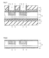
- etching stop layer 1b and second layer 1c may be removed with first layer 1a remaining in contact with first main surface 10a of silicon carbide substrate 10 as shown in Fig. 8 , or first layer 1a may be removed along with etching stop layer 1 b and second layer 1c to expose first main surface 1a of silicon carbide substrate 10 as shown in Fig. 9 .
- Third layer 2a may be removed along with fourth layer 2b and fifth layer 2c to expose second main surface 10b of silicon carbide substrate 10.
- a fourth mask layer forming step is performed.
- a fourth mask layer 4 is formed in contact with first layer 1a of first mask layer 1.
- Fourth mask layer 4 preferably includes a sixth layer 4b in contact with first layer 1a, and a seventh layer 4c in contact with sixth layer 4b opposite to first layer 1a.
- a material for sixth layer 4b may be the same as the material for etching stop layer 1b.
- a material for seventh layer 4c may be the same as the material for second layer 1c.
- a fifth mask layer 5 may be formed in contact with third layer 2a of second mask layer 2.
- Fifth mask layer 5 preferably includes an eighth layer 5b in contact with third layer 2a, and a ninth layer 5c in contact with eighth layer 5b opposite to third layer 2a.
- a material for eighth layer 5b may be the same as the material for etching stop layer 1b.
- a material for ninth layer 5c may be the same as the material for second layer 1c.
- fourth mask layer 4 and fifth mask layer 5 are simultaneously formed.
- sixth layer 4b and eighth layer 5b are simultaneously formed, and seventh layer 4c and ninth layer 5c are simultaneously formed.
- fourth mask layer 4 and fifth mask layer 5 do not include a metallic element.
- second recesses 29 are formed on an outer peripheral side of silicon carbide substrate 10.
- a side wall surface of each of second recesses 29 may be formed of sixth layer 4b and seventh layer 4c, and a bottom wall surface of each of second recesses 29 may be formed of sixth layer 4b.
- Second recesses 29 may be singular or plural in number. If there are a plurality of second recesses 29, second recesses 29 may be similar in shape when viewed from the direction of the normal of first main surface 10a.
- a guard ring region forming step is performed. Specifically, referring to Fig. 10 , Al ions, for example, are implanted into epitaxial layer 12 of silicon carbide substrate 10 using fourth mask layer 4 that has been patterned in the above step of patterning the fourth mask layer and first layer 1a of first mask layer 1, to form guard ring regions 6. Guard ring regions 6 are formed to surround body regions 14 on the outer peripheral side of silicon carbide substrate 10.
- sixth layer 4b and seventh layer 4c forming fourth mask layer 4 are removed.
- eighth layer 5b and ninth layer 5c forming fifth mask layer 5 may be removed.
- a sixth mask layer (not shown) is formed with openings above the positions where p + regions 16 in contact with source regions 15 and body regions 14 are to be formed.
- P + regions 16 may be formed by implanting Al ions, for example, into source regions 15 using the sixth mask layer.
- the sixth mask layer is removed to thereby form silicon carbide substrate 10 which has first main surface 10a covered with first layer 1a, and includes first impurity regions 14, second impurity regions 15, p + regions 16 and guard ring regions 6 formed therein.
- the sixth mask layer does not include a metallic element.
- a mask layer removing step is performed as a step (S50).
- first layer 1a of first mask layer 1 is removed from first main surface 10a of silicon carbide substrate 10
- third layer 2a of second mask layer 2 is removed from second main surface 10b. Consequently, body regions 14, source regions 15, p + regions 16 and guard ring regions 6 formed in silicon carbide substrate 10 are exposed at first main surface 10a.
- an activation annealing step is performed as a step (S60).
- silicon carbide substrate 10 having body regions 14, source regions 15, p + regions 16 and guard ring regions 6 formed therein is heated to about 1800°C in an argon atmosphere, for example, to activate the impurities introduced into body regions 14, source regions 15, p + regions 16 and guard ring regions 6. Consequently, desired carriers are generated in the regions where the impurities have been introduced.
- a gate insulating film forming step is performed as a step (S70).
- silicon carbide substrate 10 is heated to about 1300°C in an atmosphere including oxygen, for example, to form gate insulating film 20 made of silicon dioxide in contact with first main surface 10a of silicon carbide substrate 10.
- Gate insulating film 20 is provided in contact with body regions 14, source regions 15, p + regions 16 and guard ring regions 6 exposed at first main surface 10a.
- a gate electrode forming step is performed as a step (S80).
- step (S80) referring to Fig. 15 , gate electrode 30 made of polysilicon including an impurity such as phosphorous is formed on and in contact with gate insulating film 20 by low-pressure CVD, for example. Gate electrode 30 is formed to face source regions 15 and body regions 14 on gate insulating film 20. Then, interlayer insulating film 40 is formed in contact with gate electrode 30 and gate insulating film 20 by P (Plasma)-CVD, for example, so as to surround gate electrode 30. Interlayer insulating film 40 is made of silicon dioxide, for example.
- an ohmic electrode forming step is performed as a step (S90).
- this step (S90) gate insulating film 20 and interlayer insulating film 40 formed to face source regions 15 and p + regions 16 are removed by dry etching, for example.
- a metal film including Ti, Al and Si, for example is formed in contact with source regions 15, p + regions 16 and gate insulating film 20 by sputtering, for example.
- silicon carbide substrate 10 having the metal film formed thereon is heated to about 1000°C, for example, to alloy the metal film and form source electrodes 50 in ohmic contact with silicon carbide substrate 10.
- source electrode interconnect 60 is formed such that it is electrically connected to source electrodes 50.
- Source electrode interconnect 60 includes aluminum, for example, and may be formed to cover interlayer insulating film 40.
- Drain electrode 70 is formed in contact with second main surface 10b of silicon carbide substrate 10, and backside surface protecting electrode 80 electrically connected to drain electrode 70 is formed.
- MOSFET 100 according to this embodiment is manufactured in this manner.
- the silicon carbide semiconductor device may be a trench type MOSFET.
- the silicon carbide semiconductor device may be an IGBT (Insulated Gate Bipolar Transistor) or an SBD (Schottky Barrier Diode).
- IGBT Insulated Gate Bipolar Transistor
- SBD Schottky Barrier Diode
- the p type and the n type have been described as the first conductivity type and the second conductivity type in this embodiment, the p type and the n type may be the second conductivity type and the first conductivity type, respectively.
- the method of manufacturing the silicon carbide semiconductor device has been described as forming the p + regions after the step of forming the guard ring regions in this embodiment, the guard ring regions may be formed after the p + regions are formed.
- first mask layer 1 does not include a metallic element.
- mixing of a metallic element into silicon carbide substrate 10 can be suppressed to reduce metal contamination of MOSFET 100.
- second mask layer 2 is formed on second main surface 10b of silicon carbide substrate 10.
- Second mask layer 2 does not include a metallic element.
- adhesion of a metallic element to second main surface 10b of silicon carbide substrate 10 from outside can be suppressed.
- second mask layer 2 does not include a metallic element, mixing of a metallic element produced from second mask layer 2 into silicon carbide substrate 10 can be suppressed.
- second main surface 10b of silicon carbide substrate 10 is protected by second mask layer 2, direct contact of silicon carbide substrate 10 with a metallic device and the like can be prevented.
- second mask layer 2 includes third layer 2a disposed in contact with second main surface 10b and made of the same material as that for first layer 1a, fourth layer 2b disposed in contact with third layer 2a and made of the same material as that for etching stop layer 1b, and fifth layer 2c disposed in contact with the surface of fourth layer 2b opposite to the surface in contact with third layer 2a and made of the same material as that for second layer 1c.
- first mask layer 1 and second mask layer 2 can be simultaneously formed on the silicon carbide substrate, thereby simplifying the process of manufacturing MOSFET 100.
- first layer 1a, etching stop layer 1b and second layer 1c are formed without generation of plasma.
- the occurrence of roughness of first main surface 10a of silicon carbide substrate 10 can be suppressed.
- etching stop layer 1b and second layer 1c are formed by thermal chemical vapor deposition.
- etching stop layer 1b and second layer 1c can be formed in a simple manner.
- etching stop layer 1b and second layer 1c are formed by low-pressure chemical vapor deposition.
- metal contamination of MOSFET 100 can be effectively suppressed.
- first layer 1a is formed either by a method of thermally oxidizing first main surface 10a or by low-pressure thermal chemical vapor deposition.
- first layer 1a can be formed in a simple manner.
- first layer 1a is made of either silicon dioxide or silicon nitride.
- first main surface 10a of silicon carbide substrate 10 is effectively protected.
- second layer 1c is made of either silicon dioxide or silicon nitride.
- second layer 1c effectively functions as a mask layer for impurity introduction.
- etching stop layer 1b is made of polysilicon.
- third mask layer 3 with opening 19 having a width smaller than recess 9 is formed.
- N type second impurity regions 15 are formed in first impurity regions 14 using third mask layer 3.
- second impurity regions 15 can be formed in first impurity regions 14 with high position accuracy.
- fourth mask layer 4 is formed in contact with first layer 1a.
- P type guard ring regions 6 are formed in silicon carbide substrate 10 using fourth mask layer 4, with first layer 1a remaining in contact with first main surface 10a.
- guard ring regions 6 can be formed in silicon carbide substrate 10 while first main surface 10a is protected by first layer 1a.
Landscapes
- Electrodes Of Semiconductors (AREA)
- Chemical & Material Sciences (AREA)
- Chemical Kinetics & Catalysis (AREA)
- Crystallography & Structural Chemistry (AREA)
Abstract
Description
- The present invention relates to methods of manufacturing silicon carbide semiconductor devices, and more particularly to a method of manufacturing a silicon carbide semiconductor device capable of suppressing metal contamination.
- In recent years, silicon carbide has been increasingly employed as a material for a semiconductor device such as a MOSFET (Metal Oxide Semiconductor Field Effect Transistor) in order to allow a higher breakdown voltage, lower loss, the use in a high-temperature environment and the like of the semiconductor device. Silicon carbide is a wide band gap semiconductor having a band gap wider than that of silicon which has been conventionally and widely used as a material for a semiconductor device. By employing the silicon carbide as a material for a semiconductor device, therefore, a higher breakdown voltage, lower on-resistance and the like of the semiconductor device can be achieved. A semiconductor device made of silicon carbide is also advantageous in that performance degradation is small when used in a high-temperature environment as compared to a semiconductor device made of silicon.
- For example,
WO 2012/086257 (PTD 1) describes a method of manufacturing a MOSFET comprising steps of forming an etching stop layer made of titanium on a surface of a silicon carbide substrate, forming a patterned mask layer on the etching stop layer, and then implanting ions into the silicon carbide substrate using the mask layer. -
- PTD 1:
WO 2012/086257 - According to the method of manufacturing a MOSFET described in
WO 2012/086257 , however, titanium is used for the etching stop layer. After the etching stop layer is formed, therefore, part of the titanium remains in the silicon carbide substrate, resulting in the occurrence of metal contamination in the silicon carbide semiconductor device. In a silicon semiconductor device made of silicon, a metallic element that has been mixed into a silicon substrate can be removed by gettering. In a silicon carbide semiconductor device, however, a metallic element cannot be removed by gettering. It is thus required to suppress metal contamination in a silicon carbide semiconductor device more than in a silicon semiconductor device. - The present invention has been made to solve the problem described above, and an object of the present invention is to provide a method of manufacturing a silicon carbide semiconductor device capable of suppressing metal contamination.
- A method of manufacturing a silicon carbide semiconductor device according to the present invention includes the following steps. A silicon carbide substrate having a first main surface and a second main surface opposite to each other is prepared. A first mask layer is formed in contact with the first main surface of the silicon carbide substrate. The first mask layer includes a first layer disposed in contact with the first main surface, an etching stop layer disposed in contact with the first layer and made of a material different from that for the first layer, and a second layer disposed in contact with a surface of the etching stop layer opposite to the surface in contact with the first layer. A recess is formed in the first mask layer by etching the second layer and the etching stop layer. A first impurity region having a first conductivity type is formed in the silicon carbide substrate using the first mask layer with the recess. The first mask layer does not include a metallic element.
- In the method of manufacturing a silicon carbide semiconductor device according to the present invention, the first mask layer does not include a metallic element. Thus, mixing of a metallic element into the silicon carbide substrate can be suppressed to reduce metal contamination of the silicon carbide semiconductor device.
- Preferably, in the above method of manufacturing a silicon carbide semiconductor device, a second mask layer is formed on the second main surface of the silicon carbide substrate. Thus, adhesion of a metallic element to the second main surface of the silicon carbide substrate from outside can be suppressed. The second mask layer does not include a metallic element. Thus, mixing of a metallic element produced from the second mask layer into the silicon carbide substrate can be suppressed. Moreover, since the second main surface of the silicon carbide substrate is protected by the second mask layer, direct contact of the silicon carbide substrate with a metallic device and the like can be prevented.
- Preferably, in the above method of manufacturing a silicon carbide semiconductor device, the second mask layer includes a third layer disposed in contact with the second main surface and made of a same material as that for the first layer, a fourth layer disposed in contact with the third layer and made of a same material as that for the etching stop layer, and a fifth layer disposed in contact with a surface of the fourth layer opposite to the surface in contact with the third layer and made of a same material as that for the second layer. Thus, the first mask layer and the second mask layer can be simultaneously formed on the silicon carbide substrate, thereby simplifying the process of manufacturing the silicon carbide semiconductor device.
- Preferably, in the above method of manufacturing a silicon carbide semiconductor device, the first layer, the etching stop layer and the second layer are formed without generation of plasma. Thus, the occurrence of roughness of the first main surface of the silicon carbide substrate can be suppressed.
- Preferably, in the above method of manufacturing a silicon carbide semiconductor device, the etching stop layer and the second layer are formed by thermal chemical vapor deposition. Thus, the etching stop layer and the second layer can be formed in a simple manner.
- Preferably, in the above method of manufacturing a silicon carbide semiconductor device, the etching stop layer and the second layer are formed by low-pressure chemical vapor deposition. Thus, metal contamination of the silicon carbide semiconductor device can be effectively suppressed.
- Preferably, in the above method of manufacturing a silicon carbide semiconductor device, the first layer is formed either by a method of thermally oxidizing the first main surface or by low-pressure thermal chemical vapor deposition. Thus, the first layer can be formed in a simple manner.
- Preferably, in the above method of manufacturing a silicon carbide semiconductor device, the first layer is made of either silicon dioxide or silicon nitride. Thus, the first main surface of the silicon carbide substrate is effectively protected.
- Preferably, in the above method of manufacturing a silicon carbide semiconductor device, the second layer is made of either silicon dioxide or silicon nitride. Thus, the second layer effectively functions as a mask layer for impurity introduction.
- Preferably, in the above method of manufacturing a silicon carbide semiconductor device, the etching stop layer is made of polysilicon. Thus, in the step of forming the recess in the first mask layer, exposure of the first layer at a bottom wall surface of the recess can be effectively suppressed.
- Preferably, in the above method of manufacturing a silicon carbide semiconductor device, after the step of forming the first impurity region, the first mask layer is removed. After the step of removing the first mask layer, activation annealing is performed on the silicon carbide substrate. Thus, damage to the first mask layer due to the high-temperature activation annealing can be prevented.
- Preferably, in the above method of manufacturing a silicon carbide semiconductor device, after the step of forming the first impurity region, in the recess, a third mask layer with an opening having a width smaller than the recess is formed. A second impurity region having a second conductivity type different from the first conductivity type is formed in the first impurity region using the third mask layer. Thus, the second impurity region can be formed in the first impurity region with high position accuracy.
- Preferably, in the above method of manufacturing a silicon carbide semiconductor device, after the step of forming the first impurity region, a fourth mask layer is formed in contact with the first layer. A guard ring portion having the first conductivity type is formed in the silicon carbide substrate using the fourth mask layer, with the first layer remaining in contact with the first main surface. Thus, the guard ring portion can be formed in the silicon carbide substrate while the first main surface is protected by the first layer.
- As is evident from the description above, according to the present invention, a method of manufacturing a silicon carbide semiconductor device capable of suppressing metal contamination can be provided.
-
-
Fig. 1 is a schematic sectional view schematically showing the structure of a silicon carbide semiconductor device according to one embodiment of the present invention. -
Fig. 2 is a flow diagram schematically showing a method of manufacturing the silicon carbide semiconductor device according to the embodiment of the present invention. -
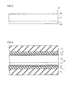
Fig. 3 is a schematic sectional view schematically showing a first step of the method of manufacturing the silicon carbide semiconductor device according to the embodiment of the present invention. -
Fig. 4 is a schematic sectional view schematically showing a second step of the method of manufacturing the silicon carbide semiconductor device according to the embodiment of the present invention. -
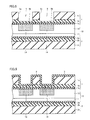
Fig. 5 is a schematic sectional view schematically showing a third step of the method of manufacturing the silicon carbide semiconductor device according to the embodiment of the present invention. -
Fig. 6 is a schematic sectional view schematically showing a fourth step of the method of manufacturing the silicon carbide semiconductor device according to the embodiment of the present invention. -
Fig. 7 is a schematic sectional view schematically showing a fifth step of the method of manufacturing the silicon carbide semiconductor device according to the embodiment of the present invention. -
Fig. 8 is a schematic sectional view schematically showing a sixth step of the method of manufacturing the silicon carbide semiconductor device according to the embodiment of the present invention. -
Fig. 9 is a schematic sectional view schematically showing a seventh step of the method of manufacturing the silicon carbide semiconductor device according to the embodiment of the present invention. -
Fig. 10 is a schematic sectional view schematically showing an eighth step of the method of manufacturing the silicon carbide semiconductor device according to the embodiment of the present invention. -
Fig. 11 is a schematic sectional view schematically showing a ninth step of the method of manufacturing the silicon carbide semiconductor device according to the embodiment of the present invention. -
Fig. 12 is a schematic sectional view schematically showing a tenth step of the method of manufacturing the silicon carbide semiconductor device according to the embodiment of the present invention. -
Fig. 13 is a schematic sectional view schematically showing an eleventh step of the method of manufacturing the silicon carbide semiconductor device according to the embodiment of the present invention. -
Fig. 14 is a schematic sectional view schematically showing a twelfth step of the method of manufacturing the silicon carbide semiconductor device according to the embodiment of the present invention. -
Fig. 15 is a schematic sectional view schematically showing a thirteenth step of the method of manufacturing the silicon carbide semiconductor device according to the embodiment of the present invention. -
Fig.16 is a schematic sectional view schematically showing a variation of the eleventh step of the method of manufacturing the silicon carbide semiconductor device according to the embodiment of the present invention. - Embodiments of the present invention will be described below with reference to the drawings. In the following drawings, the same or corresponding parts are designated by the same reference numbers and description thereof will not be repeated.
- First, the structure of a
MOSFET 100 as a silicon carbide semiconductor device according to this embodiment will be described. Referring toFig. 1 ,MOSFET 100 mainly has asilicon carbide substrate 10, agate insulating film 20, agate electrode 30, aninterlayer insulating film 40,source electrodes 50, asource electrode interconnect 60, adrain electrode 70, and a backsidesurface protecting electrode 80.Silicon carbide substrate 10 includes abase substrate 11 and anepitaxial layer 12, whereepitaxial layer 12 has adrift region 13,body regions 14,source regions 15 and p+ regions 16 formed therein. -
Base substrate 11 is a substrate of n type conductivity (second conductivity type) by including an n type impurity such as N (nitrogen).Epitaxial layer 12 is an epitaxial growth layer formed onbase substrate 11.Drift region 13 is a region of n type conductivity by including an n type impurity such as N (nitrogen), as withbase substrate 11, with a concentration of the impurity being lower than inbase substrate 11. - Body regions 14 (first impurity regions 14) include a first
main surface 10a ofsilicon carbide substrate 10, and are formed separately from each other inepitaxial layer 12. Each ofbody regions 14 has p type conductivity (first conductivity type) by including a p type impurity such as Al (aluminum) or B (boron). - Source regions 15 (second impurity regions 15) are regions of n type conductivity (second conductivity type). Each of
source regions 15 is formed in each ofbody regions 14 so as to include firstmain surface 10a and be surrounded bybody region 14.Source region 15 has n type conductivity, as withbase substrate 11 and driftregion 13, by including an n type impurity such as P (phosphorous). A concentration of the n type impurity included insource region 15 is higher than the concentration of the n type impurity included indrift region 13.Source region 15 is separated fromdrift region 13 bybody region 14. - Each of p+ regions 16 is formed in each of
body regions 14, as withsource region 15, so as to include firstmain surface 10a, be surrounded bybody region 14 and be adjacent to sourceregion 15. P+ region 16 has p type conductivity by including a p type impurity such as Al (aluminum) or B (boron), as withbody region 14. An impurity concentration in p+ region 16 is higher than inbody region 14. -
Gate insulating film 20 is made of silicon dioxide, for example, and formed to extend from an upper surface of one ofsource regions 15 to an upper surface of theother source region 15 while being in contact with firstmain surface 10a.Gate insulating film 20 is in contact withsource regions 15,body regions 14 and driftregion 13 on firstmain surface 10a. -
Gate electrode 30 is formed to extend from above one ofsource regions 15 to above theother source region 15 while being in contact withgate insulating film 20.Gate electrode 30 is made of a conductor such as polysilicon doped with an impurity such as phosphorous.Gate electrode 30 is formed such thatgate insulating film 20 is interposed betweengate electrode 30 andsilicon carbide substrate 10.Gate electrode 30 is disposed to facesource regions 15 andbody regions 14 withgate insulating film 20 interposed therebetween. -
Interlayer insulating film 40 is made of a material including silicon dioxide, for example, and formed to surroundgate electrode 30 ongate insulating film 20. Preferably,interlayer insulating film 40 is made of silicon dioxide not doped with an impurity such as phosphorous. - Each of
source electrodes 50 is in contact withsource region 15 and p+ region 16, and disposed in asecond recess 29. Preferably,source electrode 50 is a film including Ti, Al and Si, and made of a TiAISi alloy, for example.Source electrode 50 may be a film including Ni and Si, and made of a NiSi alloy, for example. Preferably,source electrode 50 is in ohmic contact withsource region 15 and p+ region 16. -
Source electrode interconnect 60 is formed to coversource electrode 50 andinterlayer insulating film 40.Source electrode interconnect 60 includes aluminum, for example, and is electrically connected to sourceelectrode 50.Source electrode interconnect 60 has a thickness of 5 µm, for example. Preferably,source electrode interconnect 60 includes a first metal layer disposed in contact withsource electrode 50. The first metal layer is preferably made of Ti (titanium). More preferably,source electrode interconnect 60 has a second metal layer disposed on and in contact with the first metal layer. The second metal layer is preferably made of TiN (titanium nitride) or TiW (titanium tungsten). The source electrode interconnect has a third metal layer disposed on and in contact with the second metal layer. The third metal layer is preferably made of AlSiCu (aluminum-silicon-copper). -
Drain electrode 70 is formed in contact with a secondmain surface 10b ofsilicon carbide substrate 10.Drain electrode 70 may be made of a TiAlSi alloy, for example, as withsource electrodes 50, or may be made of a NiSi alloy, for example.Drain electrode 70 is electrically connected tobase substrate 11. Backsidesurface protecting electrode 80 is provided in contact withdrain electrode 70. Backsidesurface protecting electrode 80 may be made of Ti (titanium), Ni (nickel) and Ag (silver), or an alloy thereof, for example. - Next, the operation of
MOSFET 100 as a silicon carbide semiconductor device according to this embodiment will be described. Referring toFig. 1 , when a voltage applied togate electrode 30 is lower than a threshold voltage, namely, in an off state, even if a voltage is applied betweensource electrode 50 anddrain electrode 70, a pn junction formed betweenbody region 14 and driftregion 13 is reverse biased, resulting in a non-conducting state. When a voltage equal to or higher than the threshold voltage is applied togate electrode 30, on the other hand, an inversion layer is formed inbody region 14. As a result,source region 15 and driftregion 13 are electrically connected together, causing a current to flow betweensource electrode 50 anddrain electrode 70.MOSFET 100 operates in this manner. - Next, a method of manufacturing the silicon carbide semiconductor device according to the embodiment of the present invention will be described with reference to
Figs. 2 to 16 . In the method of manufacturing the silicon carbide semiconductor device according to this embodiment,MOSFET 100 is manufactured as the silicon carbide semiconductor device according to this embodiment above. - Referring to
Fig. 3 , a silicon carbide substrate preparing step (S10) is first performed. In this step (S10),base substrate 11 of n type conductivity (second conductivity type) is first prepared by slicing an ingot (not shown) made of hexagonal silicon carbide having a polytype of 4H, for example. Then,epitaxial layer 12 having n type conductivity and made of silicon carbide is formed onbase substrate 11 by epitaxial growth.Silicon carbide substrate 10 having firstmain surface 10a and secondmain surface 10b opposite to each other is thus formed. - Next, a mask forming step is performed as a step (S20). In this step (S20), referring to
Fig. 4 , afirst mask layer 1 is formed in contact with firstmain surface 10a ofsilicon carbide substrate 10.First mask layer 1 includes afirst layer 1a disposed in contact with firstmain surface 10a ofsilicon carbide substrate 10. Preferably,first layer 1 a is made of either silicon dioxide or silicon nitride, and may be silicon nitride oxide.First layer 1a has a thickness of about 0.005 µm or more and 0.2 µm or less, for example.First mask layer 1 further includes anetching stop layer 1b disposed in contact with the first layer and made of a material different from that for the first layer. -
Etching stop layer 1b is made of polysilicon, for example, andetching stop layer 1b has a thickness of about 0.1 µm or more and 1.0 µm or less, for example.Etching stop layer 1b may be silicon nitride.First mask layer 1 further includes asecond layer 1c disposed in contact with a surface ofetching stop layer 1b opposite to the surface in contact withfirst layer 1a. Preferably,second layer 1c is made of either silicon dioxide or silicon nitride, and may be silicon nitride oxide.Second layer 1c has a thickness of about 0.5 µm or more and 4.0 µm or less, for example. - Preferably, in the mask forming step,
first mask layer 1 is formed in contact with firstmain surface 10a ofsilicon carbide substrate 10, and asecond mask layer 2 is formed in contact with secondmain surface 10b ofsilicon carbide substrate 10.Second mask layer 2 may include athird layer 2a disposed on secondmain surface 10b and made of the same material as that forfirst layer 1a.Second mask layer 2 may further include afourth layer 2b disposed in contact withthird layer 2a and made of the same material as that foretching stop layer 1b.Second mask layer 2 may further include afifth layer 2c disposed in contact with a surface offourth layer 2b opposite to the surface in contact withthird layer 2a and made of the same material as that forsecond layer 1c. - Preferably,
first layer 1a andthird layer 2a are simultaneously formed in contact with firstmain surface 10a and secondmain surface 10b ofsilicon carbide substrate 10, respectively. Preferably,etching stop layer 1b andfourth layer 2b are simultaneously formed in contact withfirst layer 1a andsecond layer 1c, respectively. More preferably,second layer 1c andfifth layer 2c are simultaneously formed in contact withetching stop layer 1b andfourth layer 2b, respectively.First layer 1a andsecond layer 1c may be made of the same material or different materials. Similarly,third layer 2a andfifth layer 2c may be made of the same material or different materials. - Preferably, at least one of
first layer 1a,etching stop layer 1b,second layer 1c,third layer 2a,fourth layer 2b andfifth layer 2c is formed without generation of plasma, and more preferably, all of the layers are formed without generation of plasma. Examples of methods of forming the above layers without generation of plasma include thermal chemical vapor deposition and photochemical vapor deposition. Examples of the thermal chemical vapor deposition (thermal CVD) include atmospheric thermal CVD and low-pressure thermal CVD Preferably, at least one offirst layer 1a,etching stop layer 1b,second layer 1c,third layer 2a,fourth layer 2b andfifth layer 2c is formed by low-pressure thermal CVD, and more preferably, all of the layers are formed by low-pressure thermal CVD -
First layer 1a may be formed by thermal oxidation of firstmain surface 10a ofsilicon carbide substrate 10.Third layer 2a may be formed by thermal oxidation of secondmain surface 10b ofsilicon carbide substrate 10. That is,first layer 1a is preferably formed either by a method of thermally oxidizing firstmain surface 10a ofsilicon carbide substrate 10 or by low-pressure thermal CVD Similarly,third layer 2a is preferably formed either by a method of thermally oxidizing secondmain surface 10b ofsilicon carbide substrate 10 or by low-pressure thermal CVD -
First layer 1a andsecond layer 1c formingfirst mask layer 1, andthird layer 2a andfifth layer 2c formingsecond mask layer 2 can be manufactured by low-pressure thermal CVD, for example. Specifically, silicon dioxide layers can be formed by supplying TEOS (Tetraethylorthosilicate) gas at a flow rate of about 60 sccm or more and 100 sccm or less into a chamber in whichsilicon carbide substrate 10 has been placed and setting a pressure of about 0.8 Torr or more and 1.4 Torr or less, at a temperature of about 600°C or more and 800°C or less, for example. -
Etching stop layer 1b andfourth layer 2b can be manufactured by low-pressure thermal CVD, for example. Specifically, polysilicon layers can be formed by supplying SiH4 gas at a flow rate of about 800 sccm or more and 1200 sccm or less into the chamber in whichsilicon carbide substrate 10 has been placed and setting a pressure of about 0.4 Torr or more and 0.8 Torr or less, at a temperature of about 500°C or more and 700°C or less, for example. -
First mask layer 1 does not include a metallic element. Specifically, each offirst layer 1a,etching stop layer 1b andsecond layer 1c formingfirst mask layer 1 does not include a metallic element. Preferably,second mask layer 2 does not include a metallic element. Specifically, each ofthird layer 2a,fourth layer 2b andfifth layer 2c formingsecond mask layer 2 does not include a metallic element. Preferably, the layers formingfirst mask layer 1 and the layers formingsecond mask layer 2 are made of non-metallic elements such as silicon. The metallic element as used herein refers to alkali metal, alkaline-earth metal, and transition metal, for example, and more specifically, Ti (titanium), Fe (iron), Ni, (nickel), Co (cobalt), W (tungsten), and the like. That the mask layers such asfirst mask layer 1 andsecond mask layer 2 do not include a metallic element means that a concentration of a metallic element included in each of these mask layers is 1 × 10¹¹ atoms/cm2 or less. - Next, a patterning step is performed as a step (S30). In this step (S30),
second layer 1c andetching stop layer 1b offirst mask layer 1 are etched with CF4 or CHF3, for example, to formrecesses 9 infirst mask layer 1 each having an opening at a position wherebody region 14 is formed. Each ofrecesses 9 has aside wall surface 9a and abottom wall surface 9b.Side wall surface 9a ofrecess 9 is formed ofsecond layer 1c andetching stop layer 1b, andbottom wall surface 9b ofrecess 9 is formed ofetching stop layer 1b. In other words,bottom wall surface 9b ofrecess 9 is located inetching stop layer 1b.Etching stop layer 1b is to preventfirst layer 1a from being etched by the above etching.Etching stop layer 1b has higher etching resistance with respect to CF4 or CHF3 thansecond layer 1c. - Next, an ion implantation step is performed as a step (S40). In this step (S40), referring to
Fig. 5 , Al (aluminum) ions, for example, are implanted intosilicon carbide substrate 10 usingfirst mask layer 1 withrecesses 9 as a mask, to formfirst impurity regions 14 as body regions inepitaxial layer 12 ofsilicon carbide substrate 10.First impurity regions 14 are p type (first conductivity type) regions. The Al ions are introduced intosilicon carbide substrate 10 throughetching stop layer 1b andfirst layer 1a. In portions wheresecond layer 1c remains, very few of the Al ions are introduced intosilicon carbide substrate 10 as the Al ions are masked bysecond layer 1c. - Next, a third mask layer forming step is performed. In this step, referring to
Fig. 6 , afterfirst impurity regions 14 are formed inepitaxial layer 12 in the above ion implantation step, athird mask layer 3 is formed in contact with side wall surfaces 9a and bottom wall surfaces 9b ofrecesses 9 formed infirst mask layer 1 and in contact with an upper surface ofsecond layer 1c. In other words,third mask layer 3 is formed in contact withside wall surfaces 9a formed ofsecond layer 1c andetching stop layer 1b and in contact withbottom wall surfaces 9b formed ofetching stop layer 1b.Third mask layer 3 is a silicon dioxide layer, for example.Third mask layer 3 is formed by low-pressure CVD, for example. Preferably,third mask layer 3 does not include a metallic element. - Next, referring to
Fig. 7 , anisotropic etching is performed onthird mask layer 3 from the side acrossthird mask layer 3 fromsilicon carbide substrate 10, to remove part ofthird mask layer 3 from the upper surface ofsecond layer 1c and bottom wall surfaces 9b ofrecesses 9. Consequently, in each ofrecesses 9 formed infirst mask layer 1,third mask layer 3 with anopening 19 having a dimension (namely, a width in a direction parallel to firstmain surface 10a) smaller thanrecess 9 is formed. Then, P (phosphorous) ions, for example, are implanted into each ofbody regions 14 as the first impurity regions ofsilicon carbide substrate 10 usingthird mask layer 3 andfirst mask layer 1 to a depth shallower than the depth to which the Al ions have been implanted, to form a source region assecond impurity region 15.Second impurity region 15 has the second conductivity type (n type) different from the first conductivity type (p type), and is formed such that it is separated from ntype drift region 13 byfirst impurity region 14. - In the method of manufacturing
MOSFET 100 of this embodiment,first impurity regions 14 andsecond impurity regions 15 are formed while firstmain surface 10a ofsilicon carbide substrate 10 remains covered withfirst layer 1a. Preferably,first impurity regions 14,second impurity regions 15, p+ regions 16 andguard ring regions 6 are formed while firstmain surface 10a ofsilicon carbide substrate 10 remains covered withfirst layer 1a. - Next, a mask layer partially removing step is performed. In the mask layer partially removing step, referring to
Fig. 8 ,etching stop layer 1b formed in contact withfirst layer 1a,second layer 1c formed in contact withetching stop layer 1b, andthird mask layer 3 formed in contact withetching stop layer 1b andsecond layer 1c are removed.Fourth layer 2b formed in contact withthird layer 2a andfifth layer 2c formed in contact withfourth layer 2b may also be removed. - For example, the silicon dioxide layers serving as
second layer 1 c,fifth layer 2c andthird mask layer 3 may be subjected to wet etching with hydrofluoric acid. For example, the polysilicon serving asetching stop layer 1b andfourth layer 2b may be removed by dry etching. Preferably,etching stop layer 1b,second layer 1c andthird mask layer 3 are removed in such a manner thatfirst layer 1a remains in contact withsilicon carbide substrate 10. Preferably,fourth layer 2b andfifth layer 2c are removed in such a manner thatthird layer 2a remains in contact withsilicon carbide substrate 10. - In the mask layer partially removing step, etching
stop layer 1b andsecond layer 1c may be removed withfirst layer 1a remaining in contact with firstmain surface 10a ofsilicon carbide substrate 10 as shown inFig. 8 , orfirst layer 1a may be removed along withetching stop layer 1 b andsecond layer 1c to expose firstmain surface 1a ofsilicon carbide substrate 10 as shown inFig. 9 .Third layer 2a may be removed along withfourth layer 2b andfifth layer 2c to expose secondmain surface 10b ofsilicon carbide substrate 10. - Next, referring to
Fig. 9 , a fourth mask layer forming step is performed. In the fourth mask layer forming step, afourth mask layer 4 is formed in contact withfirst layer 1a offirst mask layer 1.Fourth mask layer 4 preferably includes asixth layer 4b in contact withfirst layer 1a, and aseventh layer 4c in contact withsixth layer 4b opposite tofirst layer 1a. A material forsixth layer 4b may be the same as the material foretching stop layer 1b. A material forseventh layer 4c may be the same as the material forsecond layer 1c. - Similarly, a
fifth mask layer 5 may be formed in contact withthird layer 2a ofsecond mask layer 2.Fifth mask layer 5 preferably includes aneighth layer 5b in contact withthird layer 2a, and aninth layer 5c in contact witheighth layer 5b opposite tothird layer 2a. A material foreighth layer 5b may be the same as the material foretching stop layer 1b. A material forninth layer 5c may be the same as the material forsecond layer 1c. Preferably,fourth mask layer 4 andfifth mask layer 5 are simultaneously formed. Preferably,sixth layer 4b andeighth layer 5b are simultaneously formed, andseventh layer 4c andninth layer 5c are simultaneously formed. Preferably,fourth mask layer 4 andfifth mask layer 5 do not include a metallic element. - Next, a step of patterning the fourth mask layer is performed. In the step of patterning the fourth mask layer, second recesses 29 are formed on an outer peripheral side of
silicon carbide substrate 10. A side wall surface of each ofsecond recesses 29 may be formed ofsixth layer 4b andseventh layer 4c, and a bottom wall surface of each ofsecond recesses 29 may be formed ofsixth layer 4b.Second recesses 29 may be singular or plural in number. If there are a plurality ofsecond recesses 29, second recesses 29 may be similar in shape when viewed from the direction of the normal of firstmain surface 10a. - Next, a guard ring region forming step is performed. Specifically, referring to
Fig. 10 , Al ions, for example, are implanted intoepitaxial layer 12 ofsilicon carbide substrate 10 usingfourth mask layer 4 that has been patterned in the above step of patterning the fourth mask layer andfirst layer 1a offirst mask layer 1, to formguard ring regions 6.Guard ring regions 6 are formed to surroundbody regions 14 on the outer peripheral side ofsilicon carbide substrate 10. - Next, referring to
Fig. 11 ,sixth layer 4b andseventh layer 4c formingfourth mask layer 4 are removed. Similarly,eighth layer 5b andninth layer 5c formingfifth mask layer 5 may be removed. Then, a sixth mask layer (not shown) is formed with openings above the positions where p+ regions 16 in contact withsource regions 15 andbody regions 14 are to be formed. P+ regions 16 may be formed by implanting Al ions, for example, intosource regions 15 using the sixth mask layer. Then, referring toFig. 12 , the sixth mask layer is removed to thereby formsilicon carbide substrate 10 which has firstmain surface 10a covered withfirst layer 1a, and includesfirst impurity regions 14,second impurity regions 15, p+ regions 16 andguard ring regions 6 formed therein. Preferably, the sixth mask layer does not include a metallic element. - Next, a mask layer removing step is performed as a step (S50). In this step, referring to
Fig. 13 ,first layer 1a offirst mask layer 1 is removed from firstmain surface 10a ofsilicon carbide substrate 10, andthird layer 2a ofsecond mask layer 2 is removed from secondmain surface 10b. Consequently,body regions 14,source regions 15, p+ regions 16 andguard ring regions 6 formed insilicon carbide substrate 10 are exposed at firstmain surface 10a. - Next, an activation annealing step is performed as a step (S60). In this step,
silicon carbide substrate 10 havingbody regions 14,source regions 15, p+ regions 16 andguard ring regions 6 formed therein is heated to about 1800°C in an argon atmosphere, for example, to activate the impurities introduced intobody regions 14,source regions 15, p+ regions 16 andguard ring regions 6. Consequently, desired carriers are generated in the regions where the impurities have been introduced. - Next, a gate insulating film forming step is performed as a step (S70). In this step (S70), referring to
Fig. 14 ,silicon carbide substrate 10 is heated to about 1300°C in an atmosphere including oxygen, for example, to formgate insulating film 20 made of silicon dioxide in contact with firstmain surface 10a ofsilicon carbide substrate 10.Gate insulating film 20 is provided in contact withbody regions 14,source regions 15, p+ regions 16 andguard ring regions 6 exposed at firstmain surface 10a. - Next, a gate electrode forming step is performed as a step (S80). In this step (S80), referring to
Fig. 15 ,gate electrode 30 made of polysilicon including an impurity such as phosphorous is formed on and in contact withgate insulating film 20 by low-pressure CVD, for example.Gate electrode 30 is formed to facesource regions 15 andbody regions 14 ongate insulating film 20. Then, interlayer insulatingfilm 40 is formed in contact withgate electrode 30 andgate insulating film 20 by P (Plasma)-CVD, for example, so as to surroundgate electrode 30.Interlayer insulating film 40 is made of silicon dioxide, for example. - Next, an ohmic electrode forming step is performed as a step (S90). In this step (S90),
gate insulating film 20 andinterlayer insulating film 40 formed to facesource regions 15 and p+ regions 16 are removed by dry etching, for example. Referring toFig. 15 , a metal film including Ti, Al and Si, for example, is formed in contact withsource regions 15, p+ regions 16 andgate insulating film 20 by sputtering, for example. Then,silicon carbide substrate 10 having the metal film formed thereon is heated to about 1000°C, for example, to alloy the metal film and formsource electrodes 50 in ohmic contact withsilicon carbide substrate 10. Then,source electrode interconnect 60 is formed such that it is electrically connected to sourceelectrodes 50.Source electrode interconnect 60 includes aluminum, for example, and may be formed to coverinterlayer insulating film 40.Drain electrode 70 is formed in contact with secondmain surface 10b ofsilicon carbide substrate 10, and backsidesurface protecting electrode 80 electrically connected to drainelectrode 70 is formed.MOSFET 100 according to this embodiment is manufactured in this manner. - Although a planar type MOSFET has been described as an example of the silicon carbide semiconductor device in this embodiment, the silicon carbide semiconductor device may be a trench type MOSFET. Alternatively, the silicon carbide semiconductor device may be an IGBT (Insulated Gate Bipolar Transistor) or an SBD (Schottky Barrier Diode). Although the p type and the n type have been described as the first conductivity type and the second conductivity type in this embodiment, the p type and the n type may be the second conductivity type and the first conductivity type, respectively. Although the method of manufacturing the silicon carbide semiconductor device has been described as forming the p+ regions after the step of forming the guard ring regions in this embodiment, the guard ring regions may be formed after the p+ regions are formed.
- A function and effect of the method of manufacturing the silicon carbide semiconductor device according to this embodiment is now described.
- According to the method of manufacturing
MOSFET 100 of this embodiment,first mask layer 1 does not include a metallic element. Thus, mixing of a metallic element intosilicon carbide substrate 10 can be suppressed to reduce metal contamination ofMOSFET 100. - Further, according to the method of manufacturing
MOSFET 100 of this embodiment,second mask layer 2 is formed on secondmain surface 10b ofsilicon carbide substrate 10.Second mask layer 2 does not include a metallic element. Thus, adhesion of a metallic element to secondmain surface 10b ofsilicon carbide substrate 10 from outside can be suppressed. Further, sincesecond mask layer 2 does not include a metallic element, mixing of a metallic element produced fromsecond mask layer 2 intosilicon carbide substrate 10 can be suppressed. Moreover, since secondmain surface 10b ofsilicon carbide substrate 10 is protected bysecond mask layer 2, direct contact ofsilicon carbide substrate 10 with a metallic device and the like can be prevented. - Further, according to the method of manufacturing
MOSFET 100 of this embodiment,second mask layer 2 includesthird layer 2a disposed in contact with secondmain surface 10b and made of the same material as that forfirst layer 1a,fourth layer 2b disposed in contact withthird layer 2a and made of the same material as that foretching stop layer 1b, andfifth layer 2c disposed in contact with the surface offourth layer 2b opposite to the surface in contact withthird layer 2a and made of the same material as that forsecond layer 1c. Thus,first mask layer 1 andsecond mask layer 2 can be simultaneously formed on the silicon carbide substrate, thereby simplifying the process of manufacturingMOSFET 100. - Further, according to the method of manufacturing
MOSFET 100 of this embodiment,first layer 1a,etching stop layer 1b andsecond layer 1c are formed without generation of plasma. Thus, the occurrence of roughness of firstmain surface 10a ofsilicon carbide substrate 10 can be suppressed. - Further, according to the method of manufacturing
MOSFET 100 of this embodiment,etching stop layer 1b andsecond layer 1c are formed by thermal chemical vapor deposition. Thus,etching stop layer 1b andsecond layer 1c can be formed in a simple manner. - Further, according to the method of manufacturing
MOSFET 100 of this embodiment,etching stop layer 1b andsecond layer 1c are formed by low-pressure chemical vapor deposition. Thus, metal contamination ofMOSFET 100 can be effectively suppressed. - Further, according to the method of manufacturing
MOSFET 100 of this embodiment,first layer 1a is formed either by a method of thermally oxidizing firstmain surface 10a or by low-pressure thermal chemical vapor deposition. Thus,first layer 1a can be formed in a simple manner. - Further, according to the method of manufacturing
MOSFET 100 of this embodiment,first layer 1a is made of either silicon dioxide or silicon nitride. Thus, firstmain surface 10a ofsilicon carbide substrate 10 is effectively protected. - Further, according to the method of manufacturing
MOSFET 100 of this embodiment,second layer 1c is made of either silicon dioxide or silicon nitride. Thus,second layer 1c effectively functions as a mask layer for impurity introduction. - Further, according to the method of manufacturing
MOSFET 100 of this embodiment,etching stop layer 1b is made of polysilicon. Thus, in the step of formingrecesses 9 infirst mask layer 1, exposure offirst layer 1a at bottom wall surfaces 9b ofrecesses 9 can be effectively suppressed. - Further, according to the method of manufacturing
MOSFET 100 of this embodiment, after the step of removingfirst mask layer 1, activation annealing is performed onsilicon carbide substrate 10. Thus, damage tofirst mask layer 1 due to the high-temperature activation annealing can be prevented. - Further, according to the method of manufacturing
MOSFET 100 of this embodiment, after the step of formingfirst impurity regions 15, in each ofrecesses 9,third mask layer 3 withopening 19 having a width smaller thanrecess 9 is formed. N typesecond impurity regions 15 are formed infirst impurity regions 14 usingthird mask layer 3. Thus,second impurity regions 15 can be formed infirst impurity regions 14 with high position accuracy. - Further, according to the method of manufacturing
MOSFET 100 of this embodiment, after the step of formingfirst impurity regions 14,fourth mask layer 4 is formed in contact withfirst layer 1a. P typeguard ring regions 6 are formed insilicon carbide substrate 10 usingfourth mask layer 4, withfirst layer 1a remaining in contact with firstmain surface 10a. Thus,guard ring regions 6 can be formed insilicon carbide substrate 10 while firstmain surface 10a is protected byfirst layer 1a. - It should be understood that the embodiments disclosed herein are illustrative and non-restrictive in every respect. The scope of the present invention is defined by the terms of the claims, rather than the description above, and is intended to include any modifications within the scope and meaning equivalent to the terms of the claims.
- 1 first mask layer; 1a first layer; 1b etching stop layer; 1c second layer; 2 second mask layer; 2a third layer; 2b fourth layer; 2c fifth layer; 3 third mask layer; 4 fourth mask layer; 4b sixth layer; 4c seventh layer; 5 fifth mask layer; 5b eighth layer; 5c ninth layer; 6 guard ring region; 9 recess; 9a side wall surface; 9b bottom wall surface; 10 silicon carbide substrate; 10a first main surface; 10b second main surface; 11 base substrate; 12 epitaxial layer; 13 drift region; 14 first impurity region (body region); 15 second impurity region (source region); 16 p+ region; 19 opening; 20 gate insulating film; 29 second recess; 30 gate electrode; 40 interlayer insulating film; 50 source electrode; 60 source electrode interconnect; 70 drain electrode; 80 backside surface protecting electrode; 100 MOSFET.
Claims (13)
- A method of manufacturing a silicon carbide semiconductor device, comprising steps of:preparing a silicon carbide substrate having a first main surface and a second main surface opposite to each other;forming a first mask layer in contact with said first main surface of said silicon carbide substrate, said first mask layer including a first layer disposed in contact with said first main surface, an etching stop layer disposed in contact with said first layer and made of a material different from that for said first layer, and a second layer disposed in contact with a surface of said etching stop layer opposite to the surface in contact with said first layer;forming a recess in said first mask layer by etching said second layer and said etching stop layer; andforming a first impurity region having a first conductivity type in said silicon carbide substrate using said first mask layer with said recess, said first mask layer not including a metallic element.
- The method of manufacturing a silicon carbide semiconductor device according to claim 1, further comprising a step of forming a second mask layer on said second main surface of said silicon carbide substrate, said second mask layer not including a metallic element.
- The method of manufacturing a silicon carbide semiconductor device according to claim 2, wherein
said second mask layer includes a third layer disposed in contact with said second main surface and made of a same material as that for said first layer, a fourth layer disposed in contact with said third layer and made of a same material as that for said etching stop layer, and a fifth layer disposed in contact with a surface of said fourth layer opposite to the surface in contact with said third layer and made of a same material as that for said second layer. - The method of manufacturing a silicon carbide semiconductor device according to any one of claims 1 to 3, wherein
said first layer, said etching stop layer and said second layer are formed without generation of plasma. - The method of manufacturing a silicon carbide semiconductor device according to claim 4, wherein
said etching stop layer and said second layer are formed by thermal chemical vapor deposition. - The method of manufacturing a silicon carbide semiconductor device according to claim 5, wherein
said etching stop layer and said second layer are formed by low-pressure thermal chemical vapor deposition. - The method of manufacturing a silicon carbide semiconductor device according to any one of claims 4 to 6, wherein
said first layer is formed either by a method of thermally oxidizing said first main surface or by low-pressure chemical vapor deposition. - The method of manufacturing a silicon carbide semiconductor device according to any one of claims 1 to 7, wherein
said first layer is made of either silicon dioxide or silicon nitride. - The method of manufacturing a silicon carbide semiconductor device according to any one of claims 1 to 8, wherein
said second layer is made of either silicon dioxide or silicon nitride. - The method of manufacturing a silicon carbide semiconductor device according to any one of claims 1 to 9, wherein
said etching stop layer is made of polysilicon. - The method of manufacturing a silicon carbide semiconductor device according to any one of claims 1 to 10, further comprising steps of:after said step of forming a first impurity region, removing said first mask layer; andafter said step of removing said first mask layer, performing activation annealing on said silicon carbide substrate.
- The method of manufacturing a silicon carbide semiconductor device according to any one of claims 1 to 11, further comprising steps of:after said step of forming a first impurity region, forming, in said recess, a third mask layer with an opening having a width smaller than said recess; andforming a second impurity region having a second conductivity type different from said first conductivity type in said first impurity region using said third mask layer.
- The method of manufacturing a silicon carbide semiconductor device according to any one of claims 1 to 12, further comprising steps of:after said step of forming a first impurity region, forming a fourth mask layer in contact with said first layer; andforming a guard ring region having said first conductivity type in said silicon carbide substrate using said fourth mask layer, with said first layer remaining in contact with said first main surface.
Applications Claiming Priority (2)
| Application Number | Priority Date | Filing Date | Title |
|---|---|---|---|
| JP2013046890A JP2014175470A (en) | 2013-03-08 | 2013-03-08 | Silicon carbide semiconductor device manufacturing method |
| PCT/JP2014/050795 WO2014136477A1 (en) | 2013-03-08 | 2014-01-17 | Method for manufacturing silicon-carbide semiconductor device |
Publications (2)
| Publication Number | Publication Date |
|---|---|
| EP2966674A1 true EP2966674A1 (en) | 2016-01-13 |
| EP2966674A4 EP2966674A4 (en) | 2016-10-26 |
Family
ID=51491008
Family Applications (1)
| Application Number | Title | Priority Date | Filing Date |
|---|---|---|---|
| EP14760219.7A Withdrawn EP2966674A4 (en) | 2013-03-08 | 2014-01-17 | PROCESS FOR PRODUCING SEMICONDUCTOR DEVICE OF SILICON CARBIDE |
Country Status (5)
| Country | Link |
|---|---|
| US (1) | US9613809B2 (en) |
| EP (1) | EP2966674A4 (en) |
| JP (1) | JP2014175470A (en) |
| CN (1) | CN104981897A (en) |
| WO (1) | WO2014136477A1 (en) |
Families Citing this family (9)
| Publication number | Priority date | Publication date | Assignee | Title |
|---|---|---|---|---|
| US20150118810A1 (en) * | 2013-10-24 | 2015-04-30 | Madhur Bobde | Buried field ring field effect transistor (buf-fet) integrated with cells implanted with hole supply path |
| JP6222771B2 (en) * | 2013-11-22 | 2017-11-01 | 国立研究開発法人産業技術総合研究所 | Method for manufacturing silicon carbide semiconductor device |
| US9391135B1 (en) * | 2015-03-23 | 2016-07-12 | Semiconductor Components Industries, Llc | Semiconductor device |
| DE102015215024B4 (en) | 2015-08-06 | 2019-02-21 | Infineon Technologies Ag | Wide bandgap semiconductor device and method of operating a semiconductor device |
| US10115790B2 (en) | 2015-09-17 | 2018-10-30 | Semiconductor Components Industries, Llc | Electronic device including an insulating structure |
| US10497602B2 (en) | 2016-08-01 | 2019-12-03 | Semiconductor Components Industries, Llc | Process of forming an electronic device including forming an electronic component and removing a portion of a substrate |
| CN109643733B (en) * | 2016-08-19 | 2022-04-15 | 罗姆股份有限公司 | Semiconductor device and method for manufacturing semiconductor device |
| US10658174B2 (en) * | 2017-11-21 | 2020-05-19 | Lam Research Corporation | Atomic layer deposition and etch for reducing roughness |
| US12009389B2 (en) * | 2021-11-30 | 2024-06-11 | Wolfspeed, Inc. | Edge termination for power semiconductor devices and related fabrication methods |
Family Cites Families (11)
| Publication number | Priority date | Publication date | Assignee | Title |
|---|---|---|---|---|
| JPS4919946B1 (en) * | 1970-07-20 | 1974-05-21 | ||
| JPS4919946A (en) | 1972-06-12 | 1974-02-21 | ||
| JP2007042803A (en) * | 2005-08-02 | 2007-02-15 | Honda Motor Co Ltd | Ion implantation mask and manufacturing method thereof, silicon carbide semiconductor device using ion implantation mask and manufacturing method thereof |
| JP2008060105A (en) * | 2006-08-29 | 2008-03-13 | Shindengen Electric Mfg Co Ltd | Semiconductor device and method for manufacturing the semiconductor device |
| JP5616665B2 (en) | 2010-03-30 | 2014-10-29 | ローム株式会社 | Semiconductor device |
| JP5636752B2 (en) * | 2010-06-15 | 2014-12-10 | 日産自動車株式会社 | Semiconductor device and manufacturing method thereof |
| WO2012086257A1 (en) * | 2010-12-22 | 2012-06-28 | 住友電気工業株式会社 | Process for manufacture of silicon carbide semiconductor device |
| WO2012098759A1 (en) | 2011-01-17 | 2012-07-26 | 住友電気工業株式会社 | Method for producing silicon carbide semiconductor device |
| JP2012178389A (en) * | 2011-02-25 | 2012-09-13 | Renesas Electronics Corp | Semiconductor device |
| JP2012253291A (en) | 2011-06-07 | 2012-12-20 | Sumitomo Electric Ind Ltd | Method of manufacturing silicon carbide semiconductor device |
| JP5845714B2 (en) | 2011-08-19 | 2016-01-20 | 住友電気工業株式会社 | Method for manufacturing silicon carbide semiconductor device |
-
2013
- 2013-03-08 JP JP2013046890A patent/JP2014175470A/en active Pending
-
2014
- 2014-01-17 US US14/766,963 patent/US9613809B2/en not_active Expired - Fee Related
- 2014-01-17 EP EP14760219.7A patent/EP2966674A4/en not_active Withdrawn
- 2014-01-17 CN CN201480007925.7A patent/CN104981897A/en active Pending
- 2014-01-17 WO PCT/JP2014/050795 patent/WO2014136477A1/en not_active Ceased
Also Published As
| Publication number | Publication date |
|---|---|
| EP2966674A4 (en) | 2016-10-26 |
| US20150380247A1 (en) | 2015-12-31 |
| JP2014175470A (en) | 2014-09-22 |
| WO2014136477A1 (en) | 2014-09-12 |
| US9613809B2 (en) | 2017-04-04 |
| CN104981897A (en) | 2015-10-14 |
Similar Documents
| Publication | Publication Date | Title |
|---|---|---|
| US9613809B2 (en) | Method of manufacturing silicon carbide semiconductor device | |
| EP2966676B1 (en) | Silicon-carbide semiconductor device and manufacturing method therefor | |
| JP5525940B2 (en) | Semiconductor device and manufacturing method of semiconductor device | |
| US20160163800A1 (en) | Semiconductor device and method of manufacturing the same | |
| JP7029710B2 (en) | Semiconductor device | |
| US7915705B2 (en) | SiC semiconductor device having outer periphery structure | |
| CN109742148B (en) | Silicon carbide UMOSFET device and preparation method thereof | |
| US20130181229A1 (en) | Semiconductor device and method for manufacturing same | |
| KR101171586B1 (en) | Semiconductor device and manufacturing method therefor | |
| JP5985105B2 (en) | Semiconductor device | |
| EP2784806A1 (en) | Method for manufacturing semiconductor device | |
| JP2015076592A (en) | Silicon carbide semiconductor device and manufacturing method of the same | |
| KR102550521B1 (en) | Manufacturing method of silicon-carbide trench schottky barrier diode | |
| JP6208106B2 (en) | Semiconductor device and manufacturing method thereof | |
| JP2015201604A (en) | Silicon carbide semiconductor device and manufacturing method of the same | |
| WO2017137291A2 (en) | Method for manufacturing a semiconductor device including a self-aligned contact to doped well region | |
| JP2015204409A (en) | Silicon carbide semiconductor device and manufacturing method of the same | |
| JP2017092364A (en) | Semiconductor device and manufacturing method of semiconductor device | |
| JP6441412B2 (en) | Semiconductor device | |
| JP7563750B2 (en) | Method for manufacturing silicon carbide semiconductor device | |
| JP2016062967A (en) | Semiconductor device and manufacturing method thereof | |
| JP2016207671A (en) | Silicon carbide semiconductor device and manufacturing method of the same | |
| JP7294156B2 (en) | Semiconductor device manufacturing method | |
| JP6547469B2 (en) | Method of manufacturing silicon carbide semiconductor device |
Legal Events
| Date | Code | Title | Description |
|---|---|---|---|
| PUAI | Public reference made under article 153(3) epc to a published international application that has entered the european phase |
Free format text: ORIGINAL CODE: 0009012 |
|
| 17P | Request for examination filed |
Effective date: 20150804 |
|
| AK | Designated contracting states |
Kind code of ref document: A1 Designated state(s): AL AT BE BG CH CY CZ DE DK EE ES FI FR GB GR HR HU IE IS IT LI LT LU LV MC MK MT NL NO PL PT RO RS SE SI SK SM TR |
|
| AX | Request for extension of the european patent |
Extension state: BA ME |
|
| DAX | Request for extension of the european patent (deleted) | ||
| A4 | Supplementary search report drawn up and despatched |
Effective date: 20160927 |
|
| RIC1 | Information provided on ipc code assigned before grant |
Ipc: H01L 29/78 20060101ALI20160921BHEP Ipc: H01L 21/033 20060101ALI20160921BHEP Ipc: H01L 29/66 20060101ALI20160921BHEP Ipc: H01L 29/16 20060101ALI20160921BHEP Ipc: H01L 21/04 20060101ALI20160921BHEP Ipc: H01L 21/336 20060101AFI20160921BHEP Ipc: H01L 29/12 20060101ALI20160921BHEP Ipc: H01L 29/06 20060101ALI20160921BHEP |
|
| STAA | Information on the status of an ep patent application or granted ep patent |
Free format text: STATUS: EXAMINATION IS IN PROGRESS |
|
| 17Q | First examination report despatched |
Effective date: 20190924 |
|
| STAA | Information on the status of an ep patent application or granted ep patent |
Free format text: STATUS: THE APPLICATION HAS BEEN WITHDRAWN |
|
| 18W | Application withdrawn |
Effective date: 20191121 |