EP2965431B1 - Low glitch-noise dac - Google Patents
Low glitch-noise dac Download PDFInfo
- Publication number
- EP2965431B1 EP2965431B1 EP14713304.5A EP14713304A EP2965431B1 EP 2965431 B1 EP2965431 B1 EP 2965431B1 EP 14713304 A EP14713304 A EP 14713304A EP 2965431 B1 EP2965431 B1 EP 2965431B1
- Authority
- EP
- European Patent Office
- Prior art keywords
- stages
- current
- dac
- resistive
- stage
- Prior art date
- Legal status (The legal status is an assumption and is not a legal conclusion. Google has not performed a legal analysis and makes no representation as to the accuracy of the status listed.)
- Active
Links
- 238000000034 method Methods 0.000 claims description 27
- 230000000295 complement effect Effects 0.000 claims description 6
- 239000000758 substrate Substances 0.000 claims description 3
- 230000008878 coupling Effects 0.000 claims 8
- 238000010168 coupling process Methods 0.000 claims 8
- 238000005859 coupling reaction Methods 0.000 claims 8
- 238000010586 diagram Methods 0.000 description 22
- 238000004891 communication Methods 0.000 description 14
- 230000007423 decrease Effects 0.000 description 12
- 239000003990 capacitor Substances 0.000 description 11
- 230000003071 parasitic effect Effects 0.000 description 10
- 229920005994 diacetyl cellulose Polymers 0.000 description 7
- 230000015556 catabolic process Effects 0.000 description 4
- 238000006243 chemical reaction Methods 0.000 description 4
- 238000006731 degradation reaction Methods 0.000 description 4
- 230000008569 process Effects 0.000 description 4
- 230000004044 response Effects 0.000 description 4
- 230000001413 cellular effect Effects 0.000 description 2
- 230000007774 longterm Effects 0.000 description 2
- 238000012986 modification Methods 0.000 description 2
- 230000004048 modification Effects 0.000 description 2
- 238000007792 addition Methods 0.000 description 1
- 230000008901 benefit Effects 0.000 description 1
- 230000005540 biological transmission Effects 0.000 description 1
- 230000008859 change Effects 0.000 description 1
- 230000003247 decreasing effect Effects 0.000 description 1
- 230000002401 inhibitory effect Effects 0.000 description 1
- 230000010355 oscillation Effects 0.000 description 1
- 230000002441 reversible effect Effects 0.000 description 1
- 230000007704 transition Effects 0.000 description 1
Images


Classifications
-
- H—ELECTRICITY
- H03—ELECTRONIC CIRCUITRY
- H03M—CODING; DECODING; CODE CONVERSION IN GENERAL
- H03M1/00—Analogue/digital conversion; Digital/analogue conversion
- H03M1/66—Digital/analogue converters
- H03M1/74—Simultaneous conversion
- H03M1/78—Simultaneous conversion using ladder network
- H03M1/785—Simultaneous conversion using ladder network using resistors, i.e. R-2R ladders
-
- H—ELECTRICITY
- H03—ELECTRONIC CIRCUITRY
- H03M—CODING; DECODING; CODE CONVERSION IN GENERAL
- H03M1/00—Analogue/digital conversion; Digital/analogue conversion
- H03M1/06—Continuously compensating for, or preventing, undesired influence of physical parameters
- H03M1/08—Continuously compensating for, or preventing, undesired influence of physical parameters of noise
- H03M1/0863—Continuously compensating for, or preventing, undesired influence of physical parameters of noise of switching transients, e.g. glitches
-
- H—ELECTRICITY
- H03—ELECTRONIC CIRCUITRY
- H03M—CODING; DECODING; CODE CONVERSION IN GENERAL
- H03M1/00—Analogue/digital conversion; Digital/analogue conversion
- H03M1/66—Digital/analogue converters
- H03M1/68—Digital/analogue converters with conversions of different sensitivity, i.e. one conversion relating to the more significant digital bits and another conversion to the less significant bits
- H03M1/687—Segmented, i.e. the more significant bit converter being of the unary decoded type and the less significant bit converter being of the binary weighted type
-
- H—ELECTRICITY
- H03—ELECTRONIC CIRCUITRY
- H03M—CODING; DECODING; CODE CONVERSION IN GENERAL
- H03M1/00—Analogue/digital conversion; Digital/analogue conversion
- H03M1/66—Digital/analogue converters
- H03M1/74—Simultaneous conversion
- H03M1/742—Simultaneous conversion using current sources as quantisation value generators
- H03M1/747—Simultaneous conversion using current sources as quantisation value generators with equal currents which are switched by unary decoded digital signals
Definitions
- US 2003/001766 A1 describes a way of converting digital signals to analog signals for wireless communications.
- An apparatus comprises a resistive-ladder array to convert afirst portion of a digital input signal to a first analog output signal.
- the apparatus further includes a current-mode array to convert a second portion of the digital input signal to a second analog output signal.
- US 2012/050085 A1 describes a low power consumption DA converter including a segment type DA converter and an R-2R resistance ladder DA converter.
- the segment type DA converter is coupled to a power source voltage VDD and outputs a current signal changing in a stepwise manner according to inputted upper bits D[7 to 5].
- the R-2R resistance ladder DA converter is coupled to the segment type DA converter in series between the power source voltage VDD and a ground voltage GND, and outputs an output voltage Vout changing in a stepwise manner.
- the R-2R resistance ladder DA converter changes the output voltage Vout by raising or lowering a reference voltage Vref according to the lower bits D[4 to 0] and the current signal from the segment type DA converter.
- US 8169353 B2 describes a circuit for digital-to-analog conversion.
- the circuit includes a digital-to-analog converter (DAC).
- the DAC includes a double cascaded current source and a differential current-mode switch (DCMS).
- the circuit further includes a direct current (DC) offset stage.
- the circuit also includes a load attenuator.
- the double cascaded current source may be between the DCMS and a rail voltage.
- the present disclosure relates to electronic circuits, and more particualry to a digital-to-analog converter.
- a digital-to-analog converter is an electronic circuit that converts a digital signal to an analog signal.
- a number of parameters are used to determine the suitability of a DAC for any given application. Among these parameters are the speed at which the DAC performs the digital-to-analog conversion, the resolution of the DAC, as well as the noise generated by the DAC.
- a wireless communication device such as a cellular phone, often uses a high speed, high resolution DAC to convert a digital signal to an analog signal for further processing by the analog circuits disposed in the communication device. Glitches generated in such a DAC increase the noise floor, which in turn may interfere with the signals transmitted by the wireless communication device.
- One of the main sources of the glitch noise is the delay differences that exist between various stages of the DAC when a transition occurs at the digital input of the DAC.
- Low noise, low power, wideband, high resolution DACs are increasingly important for advanced wireless standards, such as the long term evolution (LTE) standard.
- LTE long term evolution
- the high frequency glitch noise generated by the transmitter DAC is an out-of-band noise that can fall into and desensitize the receiver channel. Controlling the glitch noise in a low-power, high resolution, wideband DAC remains a challenge.
- a digital-to-analog converter in accordance with embodiment of the present invention, includes input stages that generate the same amount of current and have similarly sized transistor switches. The currents flowing through the transistor switches and the glitch noise are therefore the same for all the input stages of the DAC.
- Input stages corresponding to the least significant bits of the DAC include resistive networks. The resistive network in each such stage scales the current it receives in accordance with the binary weight of the stage's bit position within the DAC.
- An N-bit DAC in accordance with one embodiment of the present invention, includes, in part, 2 M -1 parallel stages associated with the M most significant bits of the DAC, (N-M) stages associated with the (N-M) least significant bits of the DAC, and an impedance attenuator.
- Each of the 2 M -1 stages includes a pair of switches and is adapted to generate the same current and deliver this current to a pair of current summing nodes of the DAC via its switch pair.
- Each of the (N-M) stages includes a resistive network and generates the same current as that generated in the 2 M -1 stages.
- Each of the (N-M) stages further includes a pair of switches which have the same size as the switches in the MSB stages and are adapted to deliver the current generated in that stage to the resistive network associated with the stage in response to differential data.
- Each resistive network is operable to scale the current it receives in accordance with a binary weight of its associated stage.
- the (N-M) stages deliver their scaled currents to the pair of current summing nodes.
- the impedance attenuator includes, in part, a differential amplifier coupled to the current summing nodes and adapted to maintain the impedance of each of the current summing nodes and a voltage difference between the current summing nodes within a range defined by the gain of the differential amplifier.
- each resistive network associated with input stages whose bit positions are different by one DAC bit are coupled to one another.
- each resistive network receives a reference voltage.
- each resistive network is an R-2R network.
- the impedance attenuator further includes, in part, first and second PMOS transistors.
- the first PMOS transistor has a source terminal coupled to a first current summing node, a drain terminal coupled to a first output terminal of the DAC, and a gate terminal coupled to a first output terminal of the amplifier.
- the second PMOS transistor has a source terminal coupled to a second current summing node, a drain terminal coupled to a second output terminal of the DAC, and a gate terminal coupled to a second output terminal of the amplifier.
- each of the N stages of the DAC includes a cascode current source that generates the same current passing though the transistor switches of that stage.
- one of the transistor switches in each of the N stages is responsive to a bit representative of a true data bit received by the DAC.
- the other transistor switch in each of the N stages is responsive to a bit representative of a complement of the bit received by the DAC.
- the resistive network associated with each of only a first subset of the (N-M) stages is an R-2R network.
- the resistive network associated with each of a second subset of the (N-M) stages is coupled to the current summing nodes of the DAC. The second subset does not include the first subset.
- At least one of the (N-M) stages further includes a voltage tracking circuit adapted to track the voltages of the current summing nodes and supply the tracked voltages to the resistive network of that stage.
- the voltage tracking circuit includes first and second amplifiers.
- the first amplifier has a first input terminal coupled to the first current summing node, a second input terminal coupled to a first resistive element disposed in the resistive network of that stage, and an output terminal coupled to the first amplifier's second input terminal.
- the second amplifier has a first input terminal coupled to the second current summing node, a second input terminal coupled to a second resistive element disposed in the resistive network of that stage, and an output terminal coupled to the second amplifier's second input terminal.
- At least one of the (N-M) stages of the DAC further includes a distortion cancellation circuit adapted to cancel the current flow between a reference voltage supplying voltage to the resistive network of that stage and the current summing nodes.
- at least one of the 2 M -1 stages of the DAC further includes first and second resistive elements. The first resistive element is disposed between one of the transistor switches of that stage and the first current summing node. The second resistive element is disposed between another one of the transistor switches of that stage and the second current summing node.
- each of the (N-M) stages further includes first and second capacitive elements.
- the first capacitive element of each such stage is coupled in parallel between the terminals of a first resistive element disposed in the resistive network of that stage.
- the second capacitive element of each such stage is coupled in parallel between the terminals of a second resistive element disposed in the resistive network of that stage.
- the first and second capacitive elements of each such stage has a capacitance substantially twice a drain-to-substrate capacitance of an MOS transistor switch disposed in the DAC.
- a method of converting an N-bit digital signal to an analog signal includes, in part, forming 2 M -1 parallel stages associated with M most significant bits of the digital data, generating the same current in each of the 2 M -1 stages, and delivering the currents from the 2 M -1 stages to first and second current summing nodes via a pair of switches disposed in each such stage.
- the method further includes, forming (N-M) stages associated with (N-M) least significant bits of the digital data, and generating in each of the (N-M) stages a current that is the same as the current generated in each of the 2 M -1 stages.
- the method further includes forming (N-M) resistive networks each associated with a different one of the (N-M) stages, delivering to each of the (N-M) resistive networks the current generated in its associated stage via a pair of switches, scaling the current received by each resistive network in accordance with a binary weight of the resistive network's associated stage, and delivering the scaled currents to the pair of current summing nodes.
- the method further includes maintaining the impedance of each of the current summing nodes within a range defined by a gain value, and maintaining the voltage difference between the current summing nodes within a range defined by the gain value. The difference in the currents delivered to the current summing nodes define the value of the analog signal.
- a digital-to-analog converter in accordance with embodiment of the present invention, includes input stages that generate the same amount of current and have similarly sized transistor switches. The currents flowing through the transistor switches are therefore the same for all the input stages of the DAC.
- Input stages corresponding to the least significant bits of the DAC include resistive networks. The resistive network in each such stage scales the current it receives in accordance with the binary weight of the stage's bit position within the DAC.
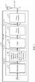
- FIG. 1 is a block diagram of a wireless communication device 150 (hereinafter alternatively referred to as device) used in a wireless communication system, in accordance with one embodiment of the present invention.
- Device 150 may be a cellular phone, a personal digital assistant (PDA), a modem, a handheld device, a laptop computer, and the like.
- PDA personal digital assistant
- Device 150 may communicate with one or more base stations on the downlink (DL) and/or uplink (UL) at any given time.
- the downlink (or forward link) refers to the communication link from a base station to the device.
- the uplink (or reverse link) refers to the communication link from the device to the base station.
- a wireless communication system may be a multiple-access system capable of supporting communication with multiple users by sharing the available system resources (e.g., bandwidth and transmit power).
- Examples of such systems include code division multiple access (CDMA) systems, time division multiple access (TDMA) systems, frequency division multiple access (FDMA) systems, orthogonal frequency division multiple access (OFDMA) systems, and spatial division multiple access (SDMA) systems.
- CDMA code division multiple access
- TDMA time division multiple access
- FDMA frequency division multiple access
- OFDMA orthogonal frequency division multiple access
- SDMA spatial division multiple access
- Wireless communication device 150 may be used in wireless communication systems such as the long term evolution (LTE) systems.
- Wireless communication system 150 may be continuously operated at high data rates or bandwidths, thus requiring an increased bandwidth for the DACs used therein.
- An increased bandwidth may require a wideband DAC implemented on a system-on-a-chip capable of handling a wide range of frequencies and digital pre-distortion operations.
- the pre-distortion operation may enable the use of low-cost non-linear power amplifiers in such wireless systems.
- Device 150 is shown as including, in part, modulator 104, DAC 100, filter 108 and amplifier 110, which collectively form a transmission channel.
- Modulator 104 is adapted to modulate incoming digital signal IN 2 and in response generate and supply the modulated signal MOD_OUT 4 to DAC 100.
- DAC 100 has a built-in load (impedance) attenuator.
- the converted signal DAC_OUT 6 supplied by DAC 100 is received and filtered by filter 108.
- the output signal FIL_OUT 8 of filter 108 is received and amplified by amplifier 110, which in response generates signal AMP1_OUT 10.
- Signal AMP1_OUT generated by amplifier 110 may be further amplified using a power amplifier 112 to generate signal AMP2_OUT before being transmitted by antenna 114.
- Low-power wireless or consumer devices may require a DAC that operates with less current.
- the dynamic linearity performance metrics that include the signal-to-noise distortion ratio (SNDR), spurious free dynamic range (SFDR) and total harmonic distortion (THD) are important system parameters.
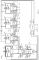
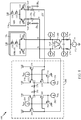
- FIG. 2 is a block diagram of a 14-bit current steering DAC 100 adapted to have a low glitch noise, in accordance with one exemplary embodiment of the present invention.
- DAC 100 may be used in device 150 shown in Figure 1 .
- DAC 100 is shown as having a 14-bit resolution, it is understood that a low glitch noise DAC, in accordance with the present invention, may have a higher or lower resolution that 14-bit.
- DAC 100 includes 63 similar input stages 110 j- j is an integer varying from 1 to 63-that are connected in parallel (for simplicity only one of the stages 110 is shown) to form the 6 most siginifcant bits (MSBs) of the DAC.
- MSBs most siginifcant bits
- DAC 100 also includes 8 stages 120 i -i is an integer varying from 1 to 8-that form the 8 least significant bits (LSBs) of the DAC.
- the 63 input stages 110 j are alternatively and collectively referred to as input stage 110.
- the 8 input stages 120 i are alternatively and collectively referred to as input stage 120. For simplicity, only three of input stages 120 i are shown.
- DAC 100 is also shown as including an output stage 190, described in detail below.
- DAC 100 is also shown as including a decoder 160 that receives a 14-bit inut signal D in [13:0] and decodes the various true D and complement bits DB that are applied to transistos 140, 145 of the various input stages 110, 120.
- Each input stage 120 i is shown as including a pair of transistors 130 and 135 that together form a cascode current source. Each input stage 120 i is also shown as including a pair of transistor switches 140 and 145 that are responsive to a pair of differential data D and DB associated with and received by the input stage. Each input stage 110 j is also shown as including a pair of transistors 130 and 135 that together form a cascode current source. Each input stage 110 j is also shown as including a pair of transistor switches 140 and 145 that are responsive to a pair of differential data D and D B associated with and received by that input stage. Transistors 130 disposed in input stages 120 i and 110 j have substantially the same size. Similarly, transistors 135 disposed in input stages 120 i and 110 j have substantially the same size. Accordingly, currents I 0 generated in stages 120 i and 110 j have the same magnitude.
- DAC 100 is also shown as including 8 resistive networks 155 i each associated with a different one of the 8 LSB stages 120.
- Each resistive networks 155 i is associated with an input stage 120 i and is adapted to scale the current the resistive network receives from its associated input stage.
- the resistive network associated with each input stage forms an R-2R network when viewed from the drain terminals of the transistor switches 140, 145 disposed in that input stage.
- stage 120 2 is shown as including R-2R resistive network 155 2 .
- stage 120 8 is shown as including R-2R resistive network 155 8 .
- each resistive network 155 i is shown as including 4 resistors, namely resistors 152 i , 154 i , 156 i , and 158 i .
- Resistors 152 i and 156 i of each input stage 120 i have a common terminal coupled to the drain terminal of transistor switch 140 i disposed in that input stage.
- resistors 154 i and 158 i of each input stage 120 i have a common terminal coupled to the drain terminal of transistor switch 145 i disposed in that input stage.
- the second terminals of resistors 152 i and 154 i receive reference voltage V ref .
- the second terminal of resistor 156 k is coupled to the drain terminal of transistor switch 140 k+1 , i.e. the transistor switch receiving the true input data D k+1 and disposed in input stage 120 k+1 having a bit position that is one higher than the bit position of input stage 120 k .
- the second terminal of resistor 158 k is coupled to the drain terminal of transistor switch 145 k+1 , i.e. the transistor switch receiving the complementary input data DB k+1 and disposed in input stage 120 k+1 .
- resistive network 155 2 associated with input stage 120 2 is shown as including resistors 152 2 , 154 2 , 156 2 , and 158 2 .
- Resistors 152 2 and 156 2 have a common terminal coupled to the drain terminal of transistor switch 140 2 disposed in input stage 120 2 .
- resistors 154 2 and 158 2 of input stage 120 2 have a common terminal coupled to the drain terminal of transistor switch 145 2 disposed in input stage 120 2 .
- the second terminals of resistors 152 2 and 154 2 receive reference voltage V ref .
- the second terminal of resistor 156 2 is coupled to the drain terminal of transistor switch 140 3 .
- the second terminal of resistor 158 2 is coupled to the drain terminal of transistor switch 145 3 .
- Resistors 152 8 and 156 8 of resistive network 155 8 associated with the last LSB stage, have a common terminal coupled to the drain terminal of transistor switch 140 8 disposed in input stage 120 8 .
- resistors 154 8 and 158 8 of each input stage 120 8 have a common terminal coupled to the drain terminal of transistor switch 145 8 disposed in input stage 120 8 .
- the second terminals of resistors 152 8 and 154 8 receive reference voltage V ref .
- the second terminal of resistor 156 8 is coupled to summing node B of output stage 190.
- the second terminal of resistor 158 8 is coupled to summing node B' of output stage 190.
- each of resistors 156 i and 158 i has a resistance R.
- Resistors 152 1 and 154 1 also have a resistance of R.
- Each of resistors 152 i and 154 i of the remaining 7 stages has a resistance of 2R. Accordingly, the resistive network 155 i associated with each input stage 120 i forms an R-2R network when viewed from the drain terminals of transistor switches 140 i and 145 i disposed in that input stage.
- each resistive network 155 i The resistances in each resistive network 155 i are selected such that the current flowing through each resistive network is proportional to the binary weight of the resistive network's associated input stage 120 i . Accordingly, if the current flowing through cascode transistors 130 and 135 of each input stage is assumed to be I 0 , the current flowing through, for example, resistors 156 8 and 158 8 disposed in resistive network 155 8 of stage 120 8 -associated with the 7 th most significant bit-into summing node B, B' is (1/2)*I 0 . Likewise, the current flowing through resistive network 155 1 of stage 120 1 -associated with the least significant bit-into summing nodes B, B' is (1/256)*I 0 .
- the currents flowing through the resistive networks 155 i are delivered to current summing nodes B, B', which provide input signals to output stage 190.
- the resistive networks are shown as being R-2R networks, however, it is understood that any other resistive network adapted to scale the current using a binary weight may be used.
- Output stage 190 in accordance with one aspect of the present invention, includes an impedance attenuator 190.
- Output stage 190 is alternatively referred to herein as impedance attenuator 190.
- the differential voltage across output nodes O, O' of impedance attenuator 190 represents the output voltage of DAC 100.
- Resistors 174, 176, together with capacitor 178 and voltage source 172 represent an output load 170.
- Current sources 162, 166 provide current I offset to nodes B, B' respectively, and current sinks 164 and 168 withdraw current I offset from node O, O' respectively.
- Current sources 162, 166, and current sinks 164, 168 are adapted to maintain the transistors disposed in attenuator 190 biased in the active regions of operation.
- the currents flowing through the transistor switches 140 and 145 in all input stages 110, 120 of the DAC are substantially the same and are scaled-after passing through the transistor switches-only by their associated resistive networks, and further because the switches 140 and 145 in all stages have the same size, the glitch energy between the MSB and LSB stages of DAC 100 are matched.
- DAC 100 thus has a substantially lower glitch noise than conventional DACs.
- the resistive networks accurately divide the currents that pass through the switches using binary weights. Resistor matching of 8-bit accuracy for the exemplary 14-bit DAC 106 is relatively easily attainable.
- each input stage 120 k Because of the R-2R network seen by each input stage 120 k , one-half of the current flowing through transistor 140 i of each input stage 120 i is supplied to voltage V ref , while the other half of this current is supplied to the drain terminal of transistor 140 (i+1) . Likewise, one-half of the current flowing through transistor 145 i of each input stage 120 i is supplied to voltage V ref , while the other half of this current is supplied to the drain terminal of transistor 145 (i+1) . Therefore, the current flowing through each resistive network 155 i is one-half the current flowing through resistive network 155 (i+1) . Accordingly, the current flowing through the resistive network in each input stage 120 i is proportional to the binary weight of the resistive network's associated input stage 120 i in the DAC.
- Impedance attenuator 190 advantageously increases the range of impedances that output load 170 may have. Impedance attenuator 190 is further adapted to account for changes in the output load impedance due to variations in the process, voltage and temperature. Consequently, since all the input stages of DAC 100 generate the same amount of current and have similar switch sizes, DAC 100 has a much smaller out-of-band noise variation across process, voltage and temperature than conventional DACs. Furthermore, impedance attenuator 190, in accordance with the present invention, provides more flexibility in selecting the resistances of resistors 152 i , 154 i , 156 i and 158 i to ensure that SFDR and SNDR of DAC 100 fall within desired values. In other words, the impedance attenuator, in accordance with the present invention, decouples the resistances of the resistive networks from the load resistance.
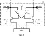
- Fig. 3 is a simplified block diagram of impedance attenuator 190 coupled to load 170.
- Impedance attenuator 190 is shown as including an amplifier 180 having a pair of differential inputs and a pair of differential outputs, and transistors 182, 184. Impedance attenuator is described in US Patent No. 8,169,353 .
- Current sources 162, 164 provide current I offset to nodes B, B' respectively, and current sinks 166 and 168 withdraw current I offset from node O, O' respectively.
- Current sources 162, 164, and current sinks 166, 168 are adapted to maintain transistors 182, 184 in the active region of operation.
- Attenuator 190 is adapted to maintain the voltage difference between nodes B, B' within a relatively small range defined by the DC gain of amplifier 180. For example, if amplifier 180 has a DC gain of 60 dB, and the voltage difference between output nodes O, O' is IV, the voltage difference between nodes B, B' is maintained at nearly 1mv, as described further below.
- DAC 100 steers more current to node B in response to a change at the input of the DAC. This causes the voltage at node B to increase. Because the input terminals of amplifier 180 have a relatively high impedance, the extra current injected into node B is cause to flow through transistor 182, thereby causing the voltage at output node O to increase. Amplifier 180 is adapted to decrease the gate voltage of PMOS transistor 182 so as to maintain the source voltage of PMOS transistor 182 relatively constant. By maintaining the source voltage of transistors 182 relatively constant, the voltage difference between nodes B, B' is maintained within a very narrow range defined by the DC gain of amplifier 180.
- impedance attenuator 190 of Figure 3 is shown as including a fully differential amplifier 180, it is understood that in other embodiments, impedance attenuator 190 may include a pair of single-ended amplifiers instead, as shown in US Patent No. 8,169,353 .
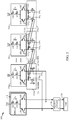
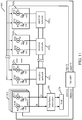
- FIG. 4 is a simplified block diagram of a current steering DAC 200 adapted to have a low glitch noise, in accordance with another exemplary embodiment of the present invention.
- DAC 200 is a 14-bit DAC shown as including, in part, 63 similar stages 110 j that are connected in parallel (only one of the stage 110 is shown) to form the 6 MSBs of DAC 200.
- DAC 200 also includes 4 stages 210 1 , 220 2 , 220 3 , 220 4 (alternatively and collectively referred to as stage 210) that form the 4 middle bits (MID) of DAC 200.
- DAC 200 also includes 4 stages 120 1 , 120 2 , 120 3 , 120 4 (alternatively and collectively referred to as stage 120 or 120 i ) that form the 4 LSBs of the DAC. Although not shown, it is understood that DAC 200 also includes a decoder similar to the one shown in Figure 2 . DAC 200 also includes an impedance attenuator 190. Although DAC 200 is shown as being a 14-bit DAC, it is understood that a low glitch noise DAC, in accordance with the presetnt invention, may have higher or fewer than 14 bits of resolution.
- Transistors 130 disposed in input stages 120 i , 110 j and 210 m have substantially the same size.
- transistors 135 disposed in input stages 120 i and 110 j and 210 m have substantially the same size. Accordingly, currents I 0 generated in all stages 120 i , 110 j and 210 m have the same magnitude.
- Input stages 120 i of DAC 200 are similar to input stages 120 i of DAC 100 (see Figure 2 ) as described above.
- Each MID stage 210 m of DAC 200 includes a resistive network 215 m that scales the current the resistive network receives from the switches disposed in its associated stage in accordance with the binary weight assigned to that stage.
- stage 210 4 is shown as including a resistive network 215 4 that scales the current it receives from its associated switches 140 4 and 145 4 to (1/2 x I 0 ) and delivers this current to summing nodes B, B' of DAC 200.
- the resistances in each resistive network associated with input stage 210 m are selected such that the current flowing through each such resistive network is proportional to the binary weight of the resistive network's associated input stage in the DAC.
- Each resistive networks 215 m is shown as including 4 resistors. Resistors 222 m and 226 m of resistive network 215 m have a common terminal coupled to the drain terminal of transistor switch 140 m disposed in input stage 210 m . Similarly, resistors 224 8 and 228 8 of each input stage 215 m have a common terminal coupled to the drain terminal of transistor switch 145 m disposed in input stage 210 m . The second terminals of resistors 222 m and 224 m receive reference voltage V ref . The second terminal of resistor 226 m is coupled to summing node B of impedance attenuator 190. Likewise, the second terminal of resistor 228 m is coupled to summing node B' of output impedance attenuator 190.
- Each of the four resistors 222 4 , 224 4 , 226 4 and 228 4 in resistive network 215 4 has a resistance of 2R. Accordingly, half of the current I o passing through transistors 140, 145 of input stage 210 4 is caused to flow to voltage V ref , while the other half of this current is caused to flow to the summing nodes B, B'. Resistors 222 3 , 224 3 of resistive network 215 3 are shown as having a resistance of 2R, and resistors 226 3 and 228 3 of resistive network 215 3 are shown as having a resistance of 6R.
- resistors 222 1 and 224 1 of input stage 210 1 are also connected to resistive network 155 4 of the LSB stage 120 4 . Accordingly, the effective resistance between the common terminal of resistors 222 1 , 226 1 and Vref is R. Likewise, the effective resistance between the common terminal of resistors 224 1 , 228 1 and Vref is R.
- Each LSB stage 120 i includes a resistive network that scales the current passing through it in accordance with the binary weight assigned to its associated input stage.
- the current scaled by each resistive network is delivered to the resistive network of the immediately preceding stage whose bit position is higher by 1 bit.
- the current scaled by resistive network 155 4 is delivered to resistive network 215 1 associated with MID stage 210 1 ;
- the current scaled by resistive network 155 3 is delivered to resistive network 155 4 ;
- the current scaled by resistive network 155 2 is delivered to resistive network 155 3 ;
- the current scaled by resistive network 155 1 is delivered to resistive network 155 2 in a chain like fashion, and as shown in Figure 4 .
- FIG. 5 is a simplified block diagram of a current-steering 14-bit DAC 300 adapted to have a low glitch noise, in accordance with another exemplary embodiment of the present invention. Although not shown, it is understood that DAC 300 also includes a decoder similar to the one shown in Figure 2 . It is also understood that DAC 300 may have a higher or lower than 14 bits of resolution.
- DAC 300 is shown as including 63 similar stages 110 that are connected in parallel to form the 6 MSBs of the DAC.
- DAC 300 further includes 8 stages 120 i that form the 8 LSBs of the DAC in a manner similar to DAC 100 of Figure 2 .
- DAC 300 dispenses the need for the reference voltage Vref and is a differential DAC.
- resistors 152 i and 154 i in each of the resistive networks 155 i are coupled to one another instead of being coupled to voltage source V ref (see Figure 2 ).
- Each of resistors 152 i , 154 i is shown as having a resistance of 2R.
- Each of resistors 152 i , 154 i is shown as having a resistance of R.
- the currents flowing through resistors 156 8 and 158 8 of resistive network 155 8 are respectively shown as being equal to [(1/4 + 1 ⁇ 2*b)*I o ] and [(1/4 + 1 ⁇ 2*(1-b))*I o ], where b is the binary value of bit 8 of the 14-bit DAC 300.
- the current generated in each of the other stages 120 i is scaled by the stage's associated resistive network and delivered to the resistive network of an immediately preceding stage whose bit position is one higher than the bit position of the stage from which it receives the current, as was also described in connection with DAC 100 of Figure 2 .
- the current scaled by resistive network 155 1 of stage 120 1 is delivered to resistive network 155 2 of stage 120 2 .
- the voltage of nodes B, B' may vary when the DAC output current varies.
- the gate-to-source capacitances of PMOS transistors 182, 184 is relatively large, nonlinear current variations at the output nodes of the impedance attenuator, i.e., gate terminals of transistors 182, 184, may get coupled to the input nodes of the impedance attenuator B, B', thereby causing the currents at nodes B, B' to vary nonlinearly.
- Such nonlinear currents may then flow through the resistive networks into voltage source V ref . Since the resistance R of the resistive networks may be smaller than the impedance of the parasitic capacitances of the DAC transistors, such current flow may degrade the SFDR of the DAC. The lower the resistance R, the larger is the degradation.
- FIG. 6 is a simplified block diagram of a segment of a DAC 400, in accordance with one embodiment of the present invention.
- DAC 400 may be, for example, a segment of DAC 100 shown in Figure 2 . Only one of the MSB stages 110 1 and one of the LSB stages 120 8 of the DAC is shown in Figure 6 but it is understood that DAC 400 has many more input stages.
- the resistive network in input stage 120 8 is adapted to include a pair of amplifiers 230 1 and 230 2 .
- the negative input terminal of amplifier 230 1 is coupled to the amplifier's output terminal and to one of the terminals of resistor 152 8 , as shown.
- the positive input terminal of amplifier 230 1 is coupled to node B.
- the negative input terminal of amplifier 230 2 is coupled to the amplifier's output terminal and to one of the terminals of resistor 154 8 , as shown.
- the positive input terminal of amplifier 230 2 is coupled to node B'. Due to the existence of virtual ground between the two input terminals of each of the two amplifiers, the output voltage of amplifier 230 1 tracks the voltage at node B, and the output voltage of amplifier 230 2 tracks the voltage at node B', thereby minimizing SFDR degradation.
- FIG. 7 is a simplified block diagram of a segment of a DAC 500, in accordance with one embodiment of the present invention.
- DAC 500 may be, for example, a segment of DAC 100 shown in Figure 2 . Only one of the MSB stages 110 1 and one of the LSB stages 120 8 of the DAC is shown in Fig. 7 but it is understood that DAC 500 has many more input stages.
- DAC 500 has disposed therein a distortion cancellation circuit 260 that includes resistors 240, 250, transistors 242, 252, amplifiers 244, 254 and capacitors 244, 156.
- Distortion cancellation circuit 260 is adapted to oppose and cancel current flow between supply voltage V ref and nodes B, B', as described further below. Any decrease in voltage V p at node B (i.e., at the positive terminal of amplifier 244) decreases the voltage at the negative terminal of amplifier 244 (source terminal of PMOS 242) due to the presence of virtual ground between the input terminals of amplifier 244, thereby causing an increase in the current flow through transistor 242. This current increase which is AC coupled to node B' via capacitor 246 flows into node B', thereby canceling the differential current flow from V ref to node B through resistors 152 8 and 158 8 .
- any increase in voltage V p at node B increases the voltage at the negative terminal of amplifier 244, thereby causing a decrease in the current flow through transistor 242.
- This current decrease which is AC coupled to node B' via capacitor 246 flows from node B', thereby canceling the differential current flow from V ref to node B through resistors 152 8 and 158 8 .
- Any increase/decrease in voltage at the source terminal of transistor 242 also causes a current flow to/from V ref via resistor 240.
- any increase/decrease in voltage at the source terminal of transistor 252 causes a current flow to/from V ref via resistor 250.
- FIG 8 is a simplified block diagram of a segment of a DAC 600, in accordance with one embodiment of the present invention.
- DAC 600 may be, for example, a segment of DAC 100 shown in Figure 2 . Only one of the MSB stages 110 1 and one of the LSB stages 120 8 of the DAC is shown in Fig. 8 but it is understood that DAC 600 has many more input stages.
- DAC 600 has disposed therein a distortion cancellation circuit 280 that includes transistors 260, 262, 264, 266, 270, 272, 274, 276, resistors 268, 278, and current sources 282, 284, 286, and 288.
- Transistors 266 and 276 that receive voltages V p and V m from nodes B, B' at their gates respectively, form the input stage to distortion cancellation circuit 280. Because the current though transistors 266 and 276 are set by current sources 282 and 286 respectively, if voltage V p increases and voltage Vm remains unchanged, the source voltage of transistor 266 at node A also increases to maintain the gate-to-source voltage of transistor 266 nearly constant. The voltage at node A' remains unchanged. Therefore, current flows from node A to node A'. The current flowing from node A to node A' is generated by transistor 262. To accommodate this extra current, the gate voltage of transistor 262 is decreased, in turn, resulting in a similar increase in the current flow through transistor 260.
- the increased current through transistor 260 increases voltage V p even further.
- the current flow from node A to node A' also causes the current though transistor 272 to decrease. Since transistor 270 and 272 also form a current mirror, the decrease in current though transistor 272 causes a similar decrease in the current though transistor 270, thereby causing a decrease in voltage V m . But as was described above, because node B' has a relatively low impedance, the decrease in voltage V m is relatively small.
- Transistor 264 is configured as a source-follower amplifier. Therefore, changes in the gate voltage of transistor 264 is reflected in corresponding voltage changes at the source of transistor 264.
- Current source 284 is adapted to flow through transistor 264.
- Transistor 274 is also configured as a source-follower amplifier. Therefore, changes in the gate voltage of transistor 274 is reflected in corresponding voltage changes at the source of transistor 274.
- Current source 288 is adapted to flow through transistor 274.
- Cancellation circuit 280 is well known and described in IEEE, International Solid-State Circuits Conferences, 1193, session 7, Analog Techniques, paper TA 7.2, pages 112-114. Although the distortion cancellation circuit is described with reference to Fig. 8 , it is understood that any other distortion cancellation circuit which performs similar constant voltage-to-current conversion may be used.
- the glitch noise and thus the glitch energy increases as the frequency of operation of a DAC increases.
- some of the glitch energy flows to the ground via the drain-to-substrate parasitic capacitors of transistors 140, 145 or parasitic capacitance of the wiring.
- the glitch energy that flows to the ground is generally less for the MSBs than the LSBs.
- the imbalance in the glitch energy that flows from different input stages of the DAC to the ground may create an imbalance that can further increase the glitch noise.
- FIG. 9 is a simplified block diagram of a segment of a DAC 700, in accordance with one embodiment of the present invention.
- DAC 700 may be, for example, a segment of DAC 100 shown in Figure 2 . Only one of the MSB stages 110 1 and one of the LSB stages 120 8 of DAC 700 is shown in Figure 9 but it is understood that DAC 700 has many more input stages.
- Figure 9 also shows the parasitic capacitances 290, 292 present between the drain terminals of transistors 140, 145 of input stage 120 8 and ground, as well as parasitic capacitances 294, 296 present between the drain terminals of transistors 140, 145 of input stage 110 1 and ground.
- resistors 112, 114 are disposed between the drain terminals of transistors 140, 145 of MSB stage 110 1 and summing nodes B, B' of DAC 700.
- Each of the resistor 112, and 114 has a resistance of R.
- Resistors 112, 114 cause the RC values seen at the drain terminals of transistors 140, 145 of input stage 120 8 to match those seen by the drain terminals of transistors 140, 145 of input stage 110 8 respectively. This RC matching inhibits the imbalance in glitch energy redistribution to ground and thus causes the glitch noise from input stage 110 1 to match that from input stage 120 8 .
- each of parallel stages 110 of DAC 700 may include resistors 112, 114.
- FIG. 10 is a simplified block diagram of a segment of a DAC 800, in accordance with one embodiment of the present invention.
- DAC 800 may be, for example, a segment of DAC 100 shown in Figure 2 . Only three of the LSB stages 120 1 and 120 2 of DAC 800 are shown in Figure 10 but it is understood that DAC 800 has many more input stages.
- Figure 10 also shows the parasitic capacitances 302 1 , 304 1 associated with transistors 140 1 , 145 1 of input stage 120 1 , parasitic capacitances 302 2 , 304 2 associated with transistors 140 2 , 145 2 of input stage 120 2 , and parasitic capacitances 302 8 , 304 8 associated with transistors 140 8 , 145 8 of input stage 120 8 .
- each input stage of DAC 800 is adapted to include a pair of capacitors 306 i , 308 i disposed in parallel between resistors 156 i and 158 i of that stage.
- capacitors 306 i , 308 1 are disposed in parallel between resistors 156 1 and 158 1 of input stage 120 1 .
- capacitors 306 8 , 308 8 are disposed in parallel between resistors 156 8 and 158 8 of input stage 120 8 .
- Capacitors 306 i , 308 i in each stage are adapted to feedforward the glitch energy so as to counter and cancel the glitch energy loss to the ground via parasitic capacitances 302 i , 304 i of that stage.
- each of the capacitors 306 i , 308 i is selected to have a capacitance twice the parasitic capacitance of capacitors 302 i , 304 i .
- FIG 11 is a block diagram of a 14-bit current steering DAC 900 adapted to have a low glitch noise, in accordance with another exemplary embodiment of the present invention.
- DAC 900 may be used in device 150 shown in Figure 1 .
- DAC 900 is shown as having a 14-bit resolution, it is understood that a low glitch noise DAC, in accordance with the presetnt invention, may have a higher or lower resolution that 14 bits.
- DAC 900 includes 63 similar input stages 910 j -j is an integer varying from 1 to 63-that are connected in parallel (for simplicity only one of the stages 910 is shown) to form the 6 most siginifcant bits (MSBs) of the DAC.
- MSBs most siginifcant bits
- DAC 900 also includes 8 stages 920 i -i is an integer varying from 1 to 8-that form the 8 least significant bits (LSBs) of the DAC.
- the 63 input stages 910 j are alternatively and collectively referred to as input stage 910.
- the 8 input stages 920 i are alternatively and collectively referred to as input stage 920. For simplicity, only three of input stages 920 i are shown.
- DAC 900 is also shown as including an impedance attenuator 190, as described in detail below.
- DAC 900 is also shown as including a decoder 160 that receives a 14-bit input signal D in [13:0] and decodes the various true D and complement bits DB that are applied to switches 940, 945 of the various input stages 910, 920.
- Each input stage 920 i is shown as including a pair of current source 930, 935.
- Each input stage 920 i is also shown as including a pair of switches 940 and 945 that are responsive to a pair of differential data D and DB associated with and received by the input stage, as well as to the currents supplied by current sources 930, 935.
- Currents I 0 generated by current source 930, 935 in stages 920 i and 910 j have substantially the same magnitude.
- DAC 900 is also shown as including 8 resistive networks 955 i each associated with a different one of the 8 LSB stages 920.
- Each resistive network 955 i is associated with an input stage 920 i and is adapted to scale the current the resistive network receives from its associated input stage.
- the resistive network associated with each input stage forms an R-2R network when viewed from switches 940, 945 disposed in that input stage.
- the resistive network associated with each stage 920 k is coupled to the resistive network of input stage 920 k+1 having a bit position that is one higher than the bit position of input stage 920 k .
- resistive network 955 2 associated with input stage 920 2 is shown as being coupled to resistive network 955 3 associated with input stage 920 3 .
- the resistive network 955 8 is coupled to summing nodes B, B' of impedance attenuator 190.
- each resistive network is proportional to the binary weight of the resistive network's associated input stage 920 i . Accordingly, if the current flowing through current sources 930 and 935 of each input stage is assumed to be I 0 , the current flowing through, for example, resistive network 955 8 of stage 920 8 -associated with the 7 th most significant bit-into summing node B, B' is (1/2)*I 0 . Likewise, the current flowing through resistive network 955 1 of stage 920 1 -associated with the least significant bit-into summing nodes B, B' is (1/256)*I 0 . The currents flowing through the resistive networks 955 i are delivered to current summing nodes B, B', which provide input signals to attenuator 190. It is understood that any resistive network adapted to scale the current using a binary weight may be used.
- DAC 900 Because the currents flowing through the switches 940 and 945 in all input stages 910, 920 of the DAC are substantially the same and are scaled (after passing through the transistor switches) only by their associated resistive networks, the glitch energy between the MSB and LSB stages of DAC 900 are matched. DAC 900 thus has a substantially lower glitch noise than conventional DACs.
- the resistive networks accurately divide the currents that pass through the switches using binary weights. Resistor matching of 8-bit accuracy for the exemplary 14-bit DAC 900 is relatively easily attainable.
- Impedance attenuator 190 advantageously increases the range of impedances that output load 170 may have. Impedance attenuator 190 is further adapted to account for changes in the output load impedance due to variations in the process, voltage and temperature. Consequently, since all the input stages of DAC 900 generate the same amount of current and have similar switch sizes, DAC 900 has a much smaller out-of-band noise variation across process, voltage and temperature than conventional DACs.
- FIG. 12 is a flowchart 1000 of a method for converting an N-bit digital signal to an analog signal, in accordance with one embodiment of the present invention.
- (2M-1) parallel stages associated with M most significant bits of the digital data are formed 1002.
- a current is generated 1004 and delivered 1006 to a pair of current summing nodes via a pair of switches that are responsive to a pair of differential data.
- (N-M) stages associated with (N-M) least significant bits of the digital data are also formed 1008.
- a current that has the same level as the ones generated in the (2M-1) parallel stages is also generated 1010 in each of the (N-M) stages.
- Also formed 1012 are (N-M) resistive networks each associated with a different one of the (N-M) stages.
- the current generated in each of the (N-M) stages is delivered 1014 to its associated resistive network via a pair of switches responsive to different bits of differential data.
- the current received by each resistive network is scaled 1016 in accordance with the binary weight of the resistive network's associated stage and delivered 1018 to the current summing nodes.
- the impedance of each of the current summing nodes is maintained 1020 within a range defined by a gain value.
- the voltage difference between the current summing nodes is also maintained 1022 within a range defined by the gain value.
- the difference in the currents delivered to the current summing nodes defines the value of the converted analog signal.
- the above embodiments of the present invention are illustrative and not limitative.
- the embodiments of the present invention are not limited by the resolution of a DAC.
- the embodiments of the present invention are not limited by the configuration of the resistive network, R-2R or otherwise, that may be disposed between input stage switches and the current summing nodes.
- the embodiments of the present invention are not limited by the type of device, wireless or otherwise, in which the DAC may be disposed.
- Other additions, subtractions or modifications are obvious in view of the present disclosure and are intended to fall within the scope of the appended claims.
Description
- This application claims the benefit of
U.S. Patent Application Serial No. 13/791,536, filed March 8, 2013 -
US 2003/001766 A1 describes a way of converting digital signals to analog signals for wireless communications. An apparatus is provided that comprises a resistive-ladder array to convert afirst portion of a digital input signal to a first analog output signal. The apparatus further includes a current-mode array to convert a second portion of the digital input signal to a second analog output signal. -
US 2012/050085 A1 describes a low power consumption DA converter including a segment type DA converter and an R-2R resistance ladder DA converter. The segment type DA converter is coupled to a power source voltage VDD and outputs a current signal changing in a stepwise manner according to inputted upper bits D[7 to 5]. The R-2R resistance ladder DA converter is coupled to the segment type DA converter in series between the power source voltage VDD and a ground voltage GND, and outputs an output voltage Vout changing in a stepwise manner. The R-2R resistance ladder DA converter changes the output voltage Vout by raising or lowering a reference voltage Vref according to the lower bits D[4 to 0] and the current signal from the segment type DA converter.US 8169353 B2 describes a circuit for digital-to-analog conversion. The circuit includes a digital-to-analog converter (DAC). The DAC includes a double cascaded current source and a differential current-mode switch (DCMS). The circuit further includes a direct current (DC) offset stage. The circuit also includes a load attenuator. The double cascaded current source may be between the DCMS and a rail voltage. - The present disclosure relates to electronic circuits, and more particualry to a digital-to-analog converter.
- A digital-to-analog converter (DAC) is an electronic circuit that converts a digital signal to an analog signal. A number of parameters are used to determine the suitability of a DAC for any given application. Among these parameters are the speed at which the DAC performs the digital-to-analog conversion, the resolution of the DAC, as well as the noise generated by the DAC.
A wireless communication device, such as a cellular phone, often uses a high speed, high resolution DAC to convert a digital signal to an analog signal for further processing by the analog circuits disposed in the communication device. Glitches generated in such a DAC increase the noise floor, which in turn may interfere with the signals transmitted by the wireless communication device. One of the main sources of the glitch noise is the delay differences that exist between various stages of the DAC when a transition occurs at the digital input of the DAC.
Low noise, low power, wideband, high resolution DACs are increasingly important for advanced wireless standards, such as the long term evolution (LTE) standard. In radio frequency (RF) applications, the high frequency glitch noise generated by the transmitter DAC is an out-of-band noise that can fall into and desensitize the receiver channel. Controlling the glitch noise in a low-power, high resolution, wideband DAC remains a challenge. - The present teaching relates to a method of converting a digital signal to an analog signal and to a corresponding digital-to-analog converter as detailed in
claims 1 and 11 respectively. A digital-to-analog converter (DAC), in accordance with embodiment of the present invention, includes input stages that generate the same amount of current and have similarly sized transistor switches. The currents flowing through the transistor switches and the glitch noise are therefore the same for all the input stages of the DAC. Input stages corresponding to the least significant bits of the DAC include resistive networks. The resistive network in each such stage scales the current it receives in accordance with the binary weight of the stage's bit position within the DAC. - An N-bit DAC, in accordance with one embodiment of the present invention, includes, in part, 2M-1 parallel stages associated with the M most significant bits of the DAC, (N-M) stages associated with the (N-M) least significant bits of the DAC, and an impedance attenuator. Each of the 2M-1 stages includes a pair of switches and is adapted to generate the same current and deliver this current to a pair of current summing nodes of the DAC via its switch pair. Each of the (N-M) stages includes a resistive network and generates the same current as that generated in the 2M-1 stages. Each of the (N-M) stages further includes a pair of switches which have the same size as the switches in the MSB stages and are adapted to deliver the current generated in that stage to the resistive network associated with the stage in response to differential data. Each resistive network is operable to scale the current it receives in accordance with a binary weight of its associated stage. The (N-M) stages deliver their scaled currents to the pair of current summing nodes. The impedance attenuator includes, in part, a differential amplifier coupled to the current summing nodes and adapted to maintain the impedance of each of the current summing nodes and a voltage difference between the current summing nodes within a range defined by the gain of the differential amplifier.
- In one embodiments, the resistive networks associated with input stages whose bit positions are different by one DAC bit are coupled to one another. In one embodiment, each resistive network receives a reference voltage. In yet another embodiment, each resistive network is an R-2R network.
- In one embodiment, the impedance attenuator further includes, in part, first and second PMOS transistors. The first PMOS transistor has a source terminal coupled to a first current summing node, a drain terminal coupled to a first output terminal of the DAC, and a gate terminal coupled to a first output terminal of the amplifier. The second PMOS transistor has a source terminal coupled to a second current summing node, a drain terminal coupled to a second output terminal of the DAC, and a gate terminal coupled to a second output terminal of the amplifier.
- In one embodiment, each of the N stages of the DAC includes a cascode current source that generates the same current passing though the transistor switches of that stage. In one embodiment, one of the transistor switches in each of the N stages is responsive to a bit representative of a true data bit received by the DAC. The other transistor switch in each of the N stages is responsive to a bit representative of a complement of the bit received by the DAC.
- In one embodiment, the resistive network associated with each of only a first subset of the (N-M) stages is an R-2R network. In another embodiment, the resistive network associated with each of a second subset of the (N-M) stages is coupled to the current summing nodes of the DAC. The second subset does not include the first subset.
- In one embodiment, at least one of the (N-M) stages further includes a voltage tracking circuit adapted to track the voltages of the current summing nodes and supply the tracked voltages to the resistive network of that stage. In one embodiment, the voltage tracking circuit includes first and second amplifiers. The first amplifier has a first input terminal coupled to the first current summing node, a second input terminal coupled to a first resistive element disposed in the resistive network of that stage, and an output terminal coupled to the first amplifier's second input terminal. The second amplifier has a first input terminal coupled to the second current summing node, a second input terminal coupled to a second resistive element disposed in the resistive network of that stage, and an output terminal coupled to the second amplifier's second input terminal.
- In one embodiment, at least one of the (N-M) stages of the DAC further includes a distortion cancellation circuit adapted to cancel the current flow between a reference voltage supplying voltage to the resistive network of that stage and the current summing nodes. In one embodiment, at least one of the 2M-1 stages of the DAC further includes first and second resistive elements. The first resistive element is disposed between one of the transistor switches of that stage and the first current summing node. The second resistive element is disposed between another one of the transistor switches of that stage and the second current summing node.
- In one embodiment, each of the (N-M) stages further includes first and second capacitive elements. The first capacitive element of each such stage is coupled in parallel between the terminals of a first resistive element disposed in the resistive network of that stage. The second capacitive element of each such stage is coupled in parallel between the terminals of a second resistive element disposed in the resistive network of that stage. In such embodiments, the first and second capacitive elements of each such stage has a capacitance substantially twice a drain-to-substrate capacitance of an MOS transistor switch disposed in the DAC.
- A method of converting an N-bit digital signal to an analog signal, in accordance with one embodiment of the present invention includes, in part, forming 2M-1 parallel stages associated with M most significant bits of the digital data, generating the same current in each of the 2M-1 stages, and delivering the currents from the 2M-1 stages to first and second current summing nodes via a pair of switches disposed in each such stage. The method further includes, forming (N-M) stages associated with (N-M) least significant bits of the digital data, and generating in each of the (N-M) stages a current that is the same as the current generated in each of the 2M-1 stages. The method further includes forming (N-M) resistive networks each associated with a different one of the (N-M) stages, delivering to each of the (N-M) resistive networks the current generated in its associated stage via a pair of switches, scaling the current received by each resistive network in accordance with a binary weight of the resistive network's associated stage, and delivering the scaled currents to the pair of current summing nodes. The method further includes maintaining the impedance of each of the current summing nodes within a range defined by a gain value, and maintaining the voltage difference between the current summing nodes within a range defined by the gain value. The difference in the currents delivered to the current summing nodes define the value of the analog signal.
- Aspects of the disclosure are illustrated by way of example. In the accompanying figures, like reference numbers indicate similar elements, and:
-
Figure 1 is a block diagram of a wireless communication device in which various aspects of the present invention may be embodied. -
Figure 2 is a simplifie block diagram of a current steering DAC adapted to have a low glitch noise, in accordance with one exemplary embodiment of the present invention. -
Figure 3 is a simplified block diagram of the impedance attenuator of the DAC shown inFigure 2 , in accordance with one exemplary embodiment of the present invention. -
Figure 4 is a simplified block diagram of a current steering DAC adapted to have a low glitch noise, in accordance with another exemplary embodiment of the present invention. -
Figure 5 is a simplified block diagram of a current-steering DAC adapted to have a low glitch noise, in accordance with another exemplary embodiment of the present invention. -
Figure 6 is a simplified block diagram of a segment of a current-steering DAC, in accordance with another exemplary embodiment of the present invention. -
Figure 7 is a simplified block diagram of a segment of a current-steering DAC, in accordance with another exemplary of the present invention. -
Figure 8 is a simplified block diagram of a segment of a current-steering DAC, in accordance with another exemplary embodiment of the present invention. -
Figure 9 is a simplified block diagram of a segment of a current-steering DAC, in accordance with another exemplary embodiment of the present invention. -
Figure 10 is a simplified block diagram of a segment of a current-steering DAC, in accordance with another exemplary embodiment of the present invention. -
Figure 11 is a simplifie block diagram of a current steering DAC adapted to have a low glitch noise, in accordance with another exemplary embodiment of the present invention. -
Figure 12 is a flowchart of a method for converting a digital signal to an analog signa, in accordance with one embodiment of the present invention. - Several illustrative embodiments will now be described with respect to the accompanying drawings, which form a part hereof. While particular embodiments, in which one or more aspects of the disclosure may be implemented, are described below, other embodiments may be used and various modifications may be made without departing from the scope of the disclosure.
- A digital-to-analog converter (DAC), in accordance with embodiment of the present invention, includes input stages that generate the same amount of current and have similarly sized transistor switches. The currents flowing through the transistor switches are therefore the same for all the input stages of the DAC. Input stages corresponding to the least significant bits of the DAC include resistive networks. The resistive network in each such stage scales the current it receives in accordance with the binary weight of the stage's bit position within the DAC.
-
Figure 1 is a block diagram of a wireless communication device 150 (hereinafter alternatively referred to as device) used in a wireless communication system, in accordance with one embodiment of the present invention.Device 150 may be a cellular phone, a personal digital assistant (PDA), a modem, a handheld device, a laptop computer, and the like. -
Device 150 may communicate with one or more base stations on the downlink (DL) and/or uplink (UL) at any given time. The downlink (or forward link) refers to the communication link from a base station to the device. The uplink (or reverse link) refers to the communication link from the device to the base station. - A wireless communication system may be a multiple-access system capable of supporting communication with multiple users by sharing the available system resources (e.g., bandwidth and transmit power). Examples of such systems include code division multiple access (CDMA) systems, time division multiple access (TDMA) systems, frequency division multiple access (FDMA) systems, orthogonal frequency division multiple access (OFDMA) systems, and spatial division multiple access (SDMA) systems.
-
Wireless communication device 150 may be used in wireless communication systems such as the long term evolution (LTE) systems.Wireless communication system 150 may be continuously operated at high data rates or bandwidths, thus requiring an increased bandwidth for the DACs used therein. An increased bandwidth may require a wideband DAC implemented on a system-on-a-chip capable of handling a wide range of frequencies and digital pre-distortion operations. The pre-distortion operation may enable the use of low-cost non-linear power amplifiers in such wireless systems. -
Device 150 is shown as including, in part,modulator 104,DAC 100,filter 108 andamplifier 110, which collectively form a transmission channel.Modulator 104 is adapted to modulate incoming digital signal IN 2 and in response generate and supply the modulated signal MOD_OUT 4 toDAC 100. As described further below,DAC 100 has a built-in load (impedance) attenuator. The converted signal DAC_OUT 6 supplied byDAC 100 is received and filtered byfilter 108. The output signal FIL_OUT 8 offilter 108 is received and amplified byamplifier 110, which in response generates signal AMP1_OUT 10. Signal AMP1_OUT generated byamplifier 110 may be further amplified using apower amplifier 112 to generate signal AMP2_OUT before being transmitted byantenna 114. - Low-power wireless or consumer devices may require a DAC that operates with less current. In such applications, the dynamic linearity performance metrics that include the signal-to-noise distortion ratio (SNDR), spurious free dynamic range (SFDR) and total harmonic distortion (THD) are important system parameters.
-
Figure 2 is a block diagram of a 14-bitcurrent steering DAC 100 adapted to have a low glitch noise, in accordance with one exemplary embodiment of the present invention.DAC 100 may be used indevice 150 shown inFigure 1 . AlthoughDAC 100 is shown as having a 14-bit resolution, it is understood that a low glitch noise DAC, in accordance with the present invention, may have a higher or lower resolution that 14-bit.DAC 100 includes 63 similar input stages 110j-j is an integer varying from 1 to 63-that are connected in parallel (for simplicity only one of thestages 110 is shown) to form the 6 most siginifcant bits (MSBs) of the DAC.DAC 100 also includes 8 stages 120i-i is an integer varying from 1 to 8-that form the 8 least significant bits (LSBs) of the DAC. The 63 input stages 110j are alternatively and collectively referred to asinput stage 110. Likewise, the 8 input stages 120i are alternatively and collectively referred to as input stage 120. For simplicity, only three of input stages 120i are shown. -
DAC 100 is also shown as including anoutput stage 190, described in detail below.DAC 100 is also shown as including adecoder 160 that receives a 14-bit inut signal Din[13:0] and decodes the various true D and complement bits DB that are applied totransistos - Each input stage 120i is shown as including a pair of
transistors transistor switches input stage 110j is also shown as including a pair oftransistors input stage 110j is also shown as including a pair oftransistor switches Transistors 130 disposed in input stages 120i and 110j have substantially the same size. Similarly,transistors 135 disposed in input stages 120i and 110j have substantially the same size. Accordingly, currents I0 generated instages 120i and 110j have the same magnitude. -
DAC 100 is also shown as including 8 resistive networks 155i each associated with a different one of the 8 LSB stages 120. Each resistive networks 155i is associated with an input stage 120i and is adapted to scale the current the resistive network receives from its associated input stage. The resistive network associated with each input stage forms an R-2R network when viewed from the drain terminals of the transistor switches 140, 145 disposed in that input stage. For example, stage 1202 is shown as including R-2R resistive network 1552. Likewise, stage 1208 is shown as including R-2R resistive network 1558. - As is seen from
Figure 2 , each resistive network 155i is shown as including 4 resistors, namely resistors 152i, 154i, 156i, and 158i. Resistors 152i and 156i of each input stage 120i have a common terminal coupled to the drain terminal oftransistor switch 140i disposed in that input stage. Similarly, resistors 154i and 158i of each input stage 120i have a common terminal coupled to the drain terminal oftransistor switch 145i disposed in that input stage. The second terminals of resistors 152i and 154i receive reference voltage Vref. For each stage 120k, where k is integer ranging from 1 to 7, the second terminal of resistor 156k is coupled to the drain terminal oftransistor switch 140k+1, i.e. the transistor switch receiving the true input data Dk+1 and disposed in input stage 120k+1 having a bit position that is one higher than the bit position of input stage 120k. Likewise, the second terminal of resistor 158k is coupled to the drain terminal oftransistor switch 145k+1, i.e. the transistor switch receiving the complementary input data DBk+1 and disposed in input stage 120k+1. - For example, resistive network 1552 associated with input stage 1202 is shown as including resistors 1522, 1542, 1562, and 1582. Resistors 1522 and 1562 have a common terminal coupled to the drain terminal of
transistor switch 1402 disposed in input stage 1202. Similarly, resistors 1542 and 1582 of input stage 1202 have a common terminal coupled to the drain terminal oftransistor switch 1452 disposed in input stage 1202. The second terminals of resistors 1522 and 1542 receive reference voltage Vref. The second terminal of resistor 1562 is coupled to the drain terminal oftransistor switch 1403. Likewise, the second terminal of resistor 1582 is coupled to the drain terminal oftransistor switch 1453. - Resistors 1528 and 1568 of resistive network 1558, associated with the last LSB stage, have a common terminal coupled to the drain terminal of
transistor switch 1408 disposed in input stage 1208. Similarly, resistors 1548 and 1588 of each input stage 1208 have a common terminal coupled to the drain terminal oftransistor switch 1458 disposed in input stage 1208. The second terminals of resistors 1528 and 1548 receive reference voltage Vref. The second terminal of resistor 1568 is coupled to summing node B ofoutput stage 190. Likewise, the second terminal of resistor 1588 is coupled to summing node B' ofoutput stage 190. - Each of resistors 156i and 158i has a resistance R. Resistors 1521 and 1541 also have a resistance of R. Each of resistors 152i and 154i of the remaining 7 stages has a resistance of 2R. Accordingly, the resistive network 155i associated with each input stage 120i forms an R-2R network when viewed from the drain terminals of
transistor switches - The resistances in each resistive network 155i are selected such that the current flowing through each resistive network is proportional to the binary weight of the resistive network's associated input stage 120i. Accordingly, if the current flowing through
cascode transistors output stage 190. In the exemplary embodiment ofDAC 100, the resistive networks are shown as being R-2R networks, however, it is understood that any other resistive network adapted to scale the current using a binary weight may be used. -
Output stage 190, in accordance with one aspect of the present invention, includes animpedance attenuator 190.Output stage 190 is alternatively referred to herein asimpedance attenuator 190. The differential voltage across output nodes O, O' ofimpedance attenuator 190 represents the output voltage ofDAC 100.Resistors capacitor 178 andvoltage source 172 represent anoutput load 170.Current sources current sinks Current sources current sinks attenuator 190 biased in the active regions of operation. - Because the currents flowing through the transistor switches 140 and 145 in all input stages 110, 120 of the DAC are substantially the same and are scaled-after passing through the transistor switches-only by their associated resistive networks, and further because the
switches DAC 100 are matched.DAC 100 thus has a substantially lower glitch noise than conventional DACs. The resistive networks accurately divide the currents that pass through the switches using binary weights. Resistor matching of 8-bit accuracy for the exemplary 14-bit DAC 106 is relatively easily attainable. - Because of the R-2R network seen by each input stage 120k, one-half of the current flowing through
transistor 140i of each input stage 120i is supplied to voltage Vref, while the other half of this current is supplied to the drain terminal oftransistor 140(i+1). Likewise, one-half of the current flowing throughtransistor 145i of each input stage 120i is supplied to voltage Vref, while the other half of this current is supplied to the drain terminal oftransistor 145(i+1). Therefore, the current flowing through each resistive network 155i is one-half the current flowing through resistive network 155(i+1). Accordingly, the current flowing through the resistive network in each input stage 120i is proportional to the binary weight of the resistive network's associated input stage 120i in the DAC. -
Impedance attenuator 190 advantageously increases the range of impedances thatoutput load 170 may have.Impedance attenuator 190 is further adapted to account for changes in the output load impedance due to variations in the process, voltage and temperature. Consequently, since all the input stages ofDAC 100 generate the same amount of current and have similar switch sizes,DAC 100 has a much smaller out-of-band noise variation across process, voltage and temperature than conventional DACs. Furthermore,impedance attenuator 190, in accordance with the present invention, provides more flexibility in selecting the resistances of resistors 152i, 154i, 156i and 158i to ensure that SFDR and SNDR ofDAC 100 fall within desired values. In other words, the impedance attenuator, in accordance with the present invention, decouples the resistances of the resistive networks from the load resistance. -
Fig. 3 is a simplified block diagram ofimpedance attenuator 190 coupled to load 170.Impedance attenuator 190 is shown as including anamplifier 180 having a pair of differential inputs and a pair of differential outputs, andtransistors US Patent No. 8,169,353 .Current sources current sinks Current sources current sinks transistors -
Attenuator 190 is adapted to maintain the voltage difference between nodes B, B' within a relatively small range defined by the DC gain ofamplifier 180. For example, ifamplifier 180 has a DC gain of 60 dB, and the voltage difference between output nodes O, O' is IV, the voltage difference between nodes B, B' is maintained at nearly 1mv, as described further below. - Assume, for example, that
DAC 100 steers more current to node B in response to a change at the input of the DAC. This causes the voltage at node B to increase. Because the input terminals ofamplifier 180 have a relatively high impedance, the extra current injected into node B is cause to flow throughtransistor 182, thereby causing the voltage at output node O to increase.Amplifier 180 is adapted to decrease the gate voltage ofPMOS transistor 182 so as to maintain the source voltage ofPMOS transistor 182 relatively constant. By maintaining the source voltage oftransistors 182 relatively constant, the voltage difference between nodes B, B' is maintained within a very narrow range defined by the DC gain ofamplifier 180. The ratio of impedance of nodes B, B' to the impedance of nodes O, O' is also defined by the gain ofamplifier 180. Althoughimpedance attenuator 190 ofFigure 3 is shown as including a fullydifferential amplifier 180, it is understood that in other embodiments,impedance attenuator 190 may include a pair of single-ended amplifiers instead, as shown inUS Patent No. 8,169,353 . -
Figure 4 is a simplified block diagram of acurrent steering DAC 200 adapted to have a low glitch noise, in accordance with another exemplary embodiment of the present invention.DAC 200 is a 14-bit DAC shown as including, in part, 63similar stages 110j that are connected in parallel (only one of thestage 110 is shown) to form the 6 MSBs ofDAC 200.DAC 200 also includes 4stages 2101, 2202, 2203, 2204 (alternatively and collectively referred to as stage 210) that form the 4 middle bits (MID) ofDAC 200.DAC 200 also includes 4 stages 1201, 1202, 1203, 1204 (alternatively and collectively referred to as stage 120 or 120i) that form the 4 LSBs of the DAC. Although not shown, it is understood thatDAC 200 also includes a decoder similar to the one shown inFigure 2 .DAC 200 also includes animpedance attenuator 190. AlthoughDAC 200 is shown as being a 14-bit DAC, it is understood that a low glitch noise DAC, in accordance with the presetnt invention, may have higher or fewer than 14 bits of resolution. -
Transistors 130 disposed in input stages 120i, 110j and 210m (m is an integer varying from 1 to 4) have substantially the same size. Similarly,transistors 135 disposed in input stages 120i and 110j and 210m have substantially the same size. Accordingly, currents I0 generated in allstages - Input stages 120i of
DAC 200 are similar to input stages 120i of DAC 100 (seeFigure 2 ) as described above. EachMID stage 210m ofDAC 200 includes a resistive network 215m that scales the current the resistive network receives from the switches disposed in its associated stage in accordance with the binary weight assigned to that stage. For example,stage 2104 is shown as including a resistive network 2154 that scales the current it receives from its associatedswitches DAC 200. The resistances in each resistive network associated withinput stage 210m are selected such that the current flowing through each such resistive network is proportional to the binary weight of the resistive network's associated input stage in the DAC. - Each resistive networks 215m is shown as including 4 resistors. Resistors 222m and 226m of resistive network 215m have a common terminal coupled to the drain terminal of
transistor switch 140m disposed ininput stage 210m. Similarly, resistors 2248 and 2288 of each input stage 215m have a common terminal coupled to the drain terminal oftransistor switch 145m disposed ininput stage 210m. The second terminals of resistors 222m and 224m receive reference voltage Vref. The second terminal of resistor 226m is coupled to summing node B ofimpedance attenuator 190. Likewise, the second terminal of resistor 228m is coupled to summing node B' ofoutput impedance attenuator 190. - Each of the four resistors 2224, 2244, 2264 and 2284 in resistive network 2154 has a resistance of 2R. Accordingly, half of the current Io passing through
transistors input stage 2104 is caused to flow to voltage Vref, while the other half of this current is caused to flow to the summing nodes B, B'. Resistors 2223, 2243 of resistive network 2153 are shown as having a resistance of 2R, and resistors 2263 and 2283 of resistive network 2153 are shown as having a resistance of 6R. Accordingly, 3/4 (i.e., 6/(6+2)) of current Io flowing throughtransistors input stage 2103 is caused to flow to voltage Vref, and 1/4 (i.e., 2/(6+2)) of current Io flowing throughtransistors input stage 2103 is caused to flow to the summing nodes B, B'. Resistors 2222, 2242 of resistive network 2152 are shown as having a resistance of 2R, and resistors 2262 and 2282 of resistive network 2152 are shown as having a resistance of 14R. Accordingly, 7/8 (i.e., 14/(14+2)) of current Io flowing throughtransistors input stage 2102 is caused to flow to voltage Vref, and 1/8 (i.e., 2/(14+2)) of current Io flowing throughtransistors input stage 2102 is caused to flow to the summing nodes B, B'. Resistors 2221, 2241 of resistive network 2151 are shown as having a resistance of 2R, and resistors 2261 and 2281 of resistive network 2151 are shown as having a resistance of 15R. However, as is seen fromFig. 4 , resistors 2221 and 2241 ofinput stage 2101 are also connected to resistive network 1554 of the LSB stage 1204. Accordingly, the effective resistance between the common terminal of resistors 2221, 2261 and Vref is R. Likewise, the effective resistance between the common terminal of resistors 2241, 2281 and Vref is R. Accordingly, 1/16 (i.e., 15/(15+1)) of current Io flowing throughtransistors input stage 2101 is caused to flow to voltage Vref, and 1/16 (i.e., 1/(15+1)) of current Io flowing throughtransistors input stage 2101 is caused to flow to summing nodes B, B'. In other words, In spite of not being R-2R networks, the resistive network associated with each of stages 2224, 2244, 2264 and 2284 provides a current to the summing nodes B, B' in proportion to the binary weight of that stage in the DAC. - Each LSB stage 120i includes a resistive network that scales the current passing through it in accordance with the binary weight assigned to its associated input stage. The current scaled by each resistive network is delivered to the resistive network of the immediately preceding stage whose bit position is higher by 1 bit. For example, the current scaled by resistive network 1554 is delivered to resistive network 2151 associated with
MID stage 2101; the current scaled by resistive network 1553 is delivered to resistive network 1554; the current scaled by resistive network 1552 is delivered to resistive network 1553; and the current scaled by resistive network 1551 is delivered to resistive network 1552 in a chain like fashion, and as shown inFigure 4 . -
Figure 5 is a simplified block diagram of a current-steering 14-bit DAC 300 adapted to have a low glitch noise, in accordance with another exemplary embodiment of the present invention. Although not shown, it is understood thatDAC 300 also includes a decoder similar to the one shown inFigure 2 . It is also understood thatDAC 300 may have a higher or lower than 14 bits of resolution. -
DAC 300 is shown as including 63similar stages 110 that are connected in parallel to form the 6 MSBs of the DAC.DAC 300 further includes 8 stages 120i that form the 8 LSBs of the DAC in a manner similar toDAC 100 ofFigure 2 .DAC 300 dispenses the need for the reference voltage Vref and is a differential DAC. As shown inFigure 5 , resistors 152i and 154i in each of the resistive networks 155i are coupled to one another instead of being coupled to voltage source Vref (seeFigure 2 ). Each of resistors 152i, 154i is shown as having a resistance of 2R. Each of resistors 152i, 154i is shown as having a resistance of R. - As is seen from
Figure 5 , for example, the currents flowing through resistors 1568 and 1588 of resistive network 1558 are respectively shown as being equal to [(1/4 + ½*b)*Io] and [(1/4 + ½*(1-b))*Io], where b is the binary value of bit 8 of the 14-bit DAC 300. As is also seen fromFigure 5 , other than stage 1208, the current generated in each of the other stages 120i is scaled by the stage's associated resistive network and delivered to the resistive network of an immediately preceding stage whose bit position is one higher than the bit position of the stage from which it receives the current, as was also described in connection withDAC 100 ofFigure 2 . For example, the current scaled by resistive network 1551 of stage 1201 is delivered to resistive network 1552 of stage 1202. - Since the amplifier disposed in the
impedance attenuator 190 of any ofDACs Fig. 3 , since the gate-to-source capacitances ofPMOS transistors transistors - To minimize the SFDR degradation due to nonlinear current flow from/to the input nodes of the impedance attenuator, in accordance with one embodiment of the present invention, the resistor voltages are tracked.
Figure 6 is a simplified block diagram of a segment of aDAC 400, in accordance with one embodiment of the present invention.DAC 400 may be, for example, a segment ofDAC 100 shown inFigure 2 . Only one of the MSB stages 1101 and one of the LSB stages 1208 of the DAC is shown inFigure 6 but it is understood thatDAC 400 has many more input stages. The resistive network in input stage 1208 is adapted to include a pair of amplifiers 2301 and 2302. The negative input terminal of amplifier 2301 is coupled to the amplifier's output terminal and to one of the terminals of resistor 1528, as shown. The positive input terminal of amplifier 2301 is coupled to node B. Likewise, the negative input terminal of amplifier 2302 is coupled to the amplifier's output terminal and to one of the terminals of resistor 1548, as shown. The positive input terminal of amplifier 2302 is coupled to node B'. Due to the existence of virtual ground between the two input terminals of each of the two amplifiers, the output voltage of amplifier 2301 tracks the voltage at node B, and the output voltage of amplifier 2302 tracks the voltage at node B', thereby minimizing SFDR degradation. In other words, because the variations in the voltage at node B is reflected at the terminal of resistor 1528, and the variations in the voltage at node B' is reflected at the terminal of resistor 1548, such voltage variations do not cause current flow from nodes B and B' to Vref, or vice versa, through the resistors-thus inhibiting SFDR degradation. Although not shown inFigure 6 , it is understood that each of the other stages 120i ofDAC 300 will share the same tracking circuit. -
Figure 7 is a simplified block diagram of a segment of aDAC 500, in accordance with one embodiment of the present invention.DAC 500 may be, for example, a segment ofDAC 100 shown inFigure 2 . Only one of the MSB stages 1101 and one of the LSB stages 1208 of the DAC is shown inFig. 7 but it is understood thatDAC 500 has many more input stages.DAC 500 has disposed therein adistortion cancellation circuit 260 that includesresistors transistors 242, 252,amplifiers capacitors 244, 156. -
Distortion cancellation circuit 260 is adapted to oppose and cancel current flow between supply voltage Vref and nodes B, B', as described further below. Any decrease in voltage Vp at node B (i.e., at the positive terminal of amplifier 244) decreases the voltage at the negative terminal of amplifier 244 (source terminal of PMOS 242) due to the presence of virtual ground between the input terminals ofamplifier 244, thereby causing an increase in the current flow through transistor 242. This current increase which is AC coupled to node B' viacapacitor 246 flows into node B', thereby canceling the differential current flow from Vref to node B through resistors 1528 and 1588. Similarly, any increase in voltage Vp at node B increases the voltage at the negative terminal ofamplifier 244, thereby causing a decrease in the current flow through transistor 242. This current decrease which is AC coupled to node B' viacapacitor 246 flows from node B', thereby canceling the differential current flow from Vref to node B through resistors 1528 and 1588. Any increase/decrease in voltage at the source terminal of transistor 242 also causes a current flow to/from Vref viaresistor 240. Likewise, any increase/decrease in voltage at the source terminal oftransistor 252 causes a current flow to/from Vref viaresistor 250. -
Figure 8 is a simplified block diagram of a segment of aDAC 600, in accordance with one embodiment of the present invention.DAC 600 may be, for example, a segment ofDAC 100 shown inFigure 2 . Only one of the MSB stages 1101 and one of the LSB stages 1208 of the DAC is shown inFig. 8 but it is understood thatDAC 600 has many more input stages.DAC 600 has disposed therein adistortion cancellation circuit 280 that includestransistors resistors current sources -
Transistors 266 and 276 that receive voltages Vp and Vm from nodes B, B' at their gates respectively, form the input stage todistortion cancellation circuit 280. Because the current thoughtransistors 266 and 276 are set bycurrent sources 282 and 286 respectively, if voltage Vp increases and voltage Vm remains unchanged, the source voltage oftransistor 266 at node A also increases to maintain the gate-to-source voltage oftransistor 266 nearly constant. The voltage at node A' remains unchanged. Therefore, current flows from node A to node A'. The current flowing from node A to node A' is generated bytransistor 262. To accommodate this extra current, the gate voltage oftransistor 262 is decreased, in turn, resulting in a similar increase in the current flow throughtransistor 260. The increased current throughtransistor 260, which forms a current mirror withtransistor 262, increases voltage Vp even further. However, because the impedance of node B is maintained at a relatively low value by the impedance attenuator, voltage Vp increases only slightly. For example, assume Vp=1.0002, Vm=999.8 mV, the load impedance is 1 k-ohm, and the impedance attenuator attenuates the impedance of the load by 1 ohm. This causes the current injected to be about 400 nA, thus increasing the voltage Vp by 200 nV (400nA/2*1ohm). Therefore, the loop gain is much smaller than unity.Distortion cancellation circuit 280 thus operates using positive feedback circuitry. The relatively small input impedances at nodes B, B' ensure that the gain of this feedback loop is smaller than unity to provide stability and prevent oscillation. - The current flow from node A to node A' also causes the current though
transistor 272 to decrease. Sincetransistor transistor 272 causes a similar decrease in the current thoughtransistor 270, thereby causing a decrease in voltage Vm. But as was described above, because node B' has a relatively low impedance, the decrease in voltage Vm is relatively small. -
Transistor 264 is configured as a source-follower amplifier. Therefore, changes in the gate voltage oftransistor 264 is reflected in corresponding voltage changes at the source oftransistor 264.Current source 284 is adapted to flow throughtransistor 264.Transistor 274 is also configured as a source-follower amplifier. Therefore, changes in the gate voltage oftransistor 274 is reflected in corresponding voltage changes at the source oftransistor 274.Current source 288 is adapted to flow throughtransistor 274.Cancellation circuit 280 is well known and described in IEEE, International Solid-State Circuits Conferences, 1193,session 7, Analog Techniques, paper TA 7.2, pages 112-114. Although the distortion cancellation circuit is described with reference toFig. 8 , it is understood that any other distortion cancellation circuit which performs similar constant voltage-to-current conversion may be used. - As is known, the glitch noise and thus the glitch energy increases as the frequency of operation of a DAC increases. Referring, for example, to
Figure 2 , as the frequency of operation increases, some of the glitch energy flows to the ground via the drain-to-substrate parasitic capacitors oftransistors -
Figure 9 is a simplified block diagram of a segment of aDAC 700, in accordance with one embodiment of the present invention.DAC 700 may be, for example, a segment ofDAC 100 shown inFigure 2 . Only one of the MSB stages 1101 and one of the LSB stages 1208 ofDAC 700 is shown inFigure 9 but it is understood thatDAC 700 has many more input stages.Figure 9 also shows theparasitic capacitances 290, 292 present between the drain terminals oftransistors parasitic capacitances transistors input stage 1101 and ground. - To minimize the glitch noise caused by the imbalance in the glitch energy that flows from input stages 1208, 1101 to the ground, in accordance with one embodiment of the present invention,
resistors transistors MSB stage 1101 and summing nodes B, B' ofDAC 700. Each of theresistor R. Resistors transistors transistors input stage 1108 respectively. This RC matching inhibits the imbalance in glitch energy redistribution to ground and thus causes the glitch noise frominput stage 1101 to match that from input stage 1208. It is understood that each ofparallel stages 110 ofDAC 700 may includeresistors -
Figure 10 is a simplified block diagram of a segment of aDAC 800, in accordance with one embodiment of the present invention.DAC 800 may be, for example, a segment ofDAC 100 shown inFigure 2 . Only three of the LSB stages 1201 and 1202 ofDAC 800 are shown inFigure 10 but it is understood thatDAC 800 has many more input stages.Figure 10 also shows the parasitic capacitances 3021, 3041 associated withtransistors transistors transistors DAC 800 is adapted to include a pair of capacitors 306i, 308i disposed in parallel between resistors 156i and 158i of that stage. For example, as shown, capacitors 306i, 3081 are disposed in parallel between resistors 1561 and 1581 of input stage 1201. Likewise, capacitors 3068, 3088 are disposed in parallel between resistors 1568 and 1588 of input stage 1208. Capacitors 306i, 308i in each stage are adapted to feedforward the glitch energy so as to counter and cancel the glitch energy loss to the ground via parasitic capacitances 302i, 304i of that stage. In one embodiment each of the capacitors 306i, 308i is selected to have a capacitance twice the parasitic capacitance of capacitors 302i, 304i. -
Figure 11 is a block diagram of a 14-bitcurrent steering DAC 900 adapted to have a low glitch noise, in accordance with another exemplary embodiment of the present invention.DAC 900 may be used indevice 150 shown inFigure 1 . AlthoughDAC 900 is shown as having a 14-bit resolution, it is understood that a low glitch noise DAC, in accordance with the presetnt invention, may have a higher or lower resolution that 14 bits.DAC 900 includes 63 similar input stages 910j-j is an integer varying from 1 to 63-that are connected in parallel (for simplicity only one of thestages 910 is shown) to form the 6 most siginifcant bits (MSBs) of the DAC.DAC 900 also includes 8 stages 920i-i is an integer varying from 1 to 8-that form the 8 least significant bits (LSBs) of the DAC. The 63 input stages 910j are alternatively and collectively referred to asinput stage 910. Likewise, the 8 input stages 920i are alternatively and collectively referred to as input stage 920. For simplicity, only three of input stages 920i are shown. -
DAC 900 is also shown as including animpedance attenuator 190, as described in detail below.DAC 900 is also shown as including adecoder 160 that receives a 14-bit input signal Din[13:0] and decodes the various true D and complement bits DB that are applied toswitches - Each input stage 920i is shown as including a pair of
current source switches current sources current source stages 920i and 910j have substantially the same magnitude. -
DAC 900 is also shown as including 8 resistive networks 955i each associated with a different one of the 8 LSB stages 920. Each resistive network 955i is associated with an input stage 920i and is adapted to scale the current the resistive network receives from its associated input stage. In one embodiment, the resistive network associated with each input stage forms an R-2R network when viewed fromswitches - As is seen from
Figure 11 , the resistive network associated with each stage 920k, where k is integer ranging from 1 to 7, is coupled to the resistive network of input stage 920k+1 having a bit position that is one higher than the bit position of input stage 920k. For example, resistive network 9552 associated with input stage 9202 is shown as being coupled to resistive network 9553 associated with input stage 9203. The resistive network 9558 is coupled to summing nodes B, B' ofimpedance attenuator 190. - The current flowing through each resistive network is proportional to the binary weight of the resistive network's associated input stage 920i. Accordingly, if the current flowing through
current sources attenuator 190. It is understood that any resistive network adapted to scale the current using a binary weight may be used. - Because the currents flowing through the
switches DAC 900 are matched.DAC 900 thus has a substantially lower glitch noise than conventional DACs. The resistive networks accurately divide the currents that pass through the switches using binary weights. Resistor matching of 8-bit accuracy for the exemplary 14-bit DAC 900 is relatively easily attainable. -
Impedance attenuator 190 advantageously increases the range of impedances thatoutput load 170 may have.Impedance attenuator 190 is further adapted to account for changes in the output load impedance due to variations in the process, voltage and temperature. Consequently, since all the input stages ofDAC 900 generate the same amount of current and have similar switch sizes,DAC 900 has a much smaller out-of-band noise variation across process, voltage and temperature than conventional DACs. -
Figure 12 is a flowchart 1000 of a method for converting an N-bit digital signal to an analog signal, in accordance with one embodiment of the present invention. To achieve this conversion, (2M-1) parallel stages associated with M most significant bits of the digital data are formed 1002. In each of the (2M-1) stages a current is generated 1004 and delivered 1006 to a pair of current summing nodes via a pair of switches that are responsive to a pair of differential data. Further in accordance with the method, (N-M) stages associated with (N-M) least significant bits of the digital data are also formed 1008. A current that has the same level as the ones generated in the (2M-1) parallel stages is also generated 1010 in each of the (N-M) stages. Also formed 1012 are (N-M) resistive networks each associated with a different one of the (N-M) stages. The current generated in each of the (N-M) stages is delivered 1014 to its associated resistive network via a pair of switches responsive to different bits of differential data. The current received by each resistive network is scaled 1016 in accordance with the binary weight of the resistive network's associated stage and delivered 1018 to the current summing nodes. The impedance of each of the current summing nodes is maintained 1020 within a range defined by a gain value. Moreover, the voltage difference between the current summing nodes is also maintained 1022 within a range defined by the gain value. The difference in the currents delivered to the current summing nodes defines the value of the converted analog signal. - The above embodiments of the present invention are illustrative and not limitative. The embodiments of the present invention are not limited by the resolution of a DAC. The embodiments of the present invention are not limited by the configuration of the resistive network, R-2R or otherwise, that may be disposed between input stage switches and the current summing nodes. The embodiments of the present invention are not limited by the type of device, wireless or otherwise, in which the DAC may be disposed. Other additions, subtractions or modifications are obvious in view of the present disclosure and are intended to fall within the scope of the appended claims.
Claims (14)
- A method of converting a digital signal (4) to an analog signal (6), the method comprising:forming (1002) a first plurality of parallel stages (110) associated with most significant bits of the digital data;generating (1004) a current of a specific size in each of the first plurality of parallel stages;delivering (1006) the current of said specified size generated in each of the first plurality of parallel stages to a pair of current summing nodes (B, B') via a pair of transistor switches (140, 145) responsive to differential data;forming (1008) a second plurality of stages (120) associated with least significant bits of the digital data;generating (1010) a current of said specified size in each of the second plurality of stages;forming (1012) a first plurality of resistive networks (155) each associated with a different one of the second plurality of stages;delivering (1014) to each of the first plurality of resistive networks the current of said specified size generated in its associated stage via a pair of transistor switches (140, 145) responsive to differential data;scaling (1016) the current received by each of the first plurality of resistive network in accordance with a binary weight of the resistive network's associated stage, delivering (1018) the scaled currents to the pair of current summing nodes (B, B');maintaining (1020) an impedance of each of the current summing nodes within a range defined by a gain value; andmaintaining (1022) a voltage difference between the current summing nodes within a range defined by the gain value, the difference in the currents delivered to the current summing nodes defining a value of the analog signal;the method further comprising:coupling a first resistive element (112) between a first (140) one of the transistor switches of at least one of the first plurality of stages (110) and a first (B) one of the current summing nodes; andcoupling a second resistive element (114) between a second (145) one of the transistor switches of the at least one of the first plurality stages and a second (B') one of the current summing nodes; andcoupling a third resistive element (158) of the first plurality of resistive networks (155) between a first (140) one of the transistor switches of at least one of the second plurality of stages (120) and the first (B) one of the current summing nodes; and coupling a fourth resistive element (156) of the first plurality of resistive networks (155) between a second (145) one of the transistor switches of the at least one of the second plurality of stages and the second (B') one of the current summing nodes;wherein each of the first resistor, the second resistor, the third resistor and the fourth resistor has the same resistance value.
- The method of claim 1 the converting a digital signal (4) to an analog signal (6) comprising converting an N-bit digital signal to an analog signal;
the first plurality of parallel stages (110) associated with most significant bits of the digital data comprising 2M-1 parallel stages (110) associated with M most significant bits of the digital data;
the second plurality of stages (120) associated with least significant bits of the digital data comprising N minus M stages (120) associated with N minus M least significant bits of the digital data. - The method of claim 2 further comprising:coupling the resistive network (155i) associated with stage i of the N minus M stages (120) to the resistive network (155i+i) of stage i+1 of the N minus M stages, wherein i is an integer representative of a bit position of the stage; orthe method of claim 2 wherein the resistive network associated with each of the N minus M stages is an R-2R network; orthe method of claim 2 further comprising:forming a cascode current source in each of the N stages (110, 120); andgenerating the current of said specified size in each of the N stages using the cascode current source formed in the stage.
- The method of claim 2 wherein in each of the stages (110, 120), one of which transistors (140) is responsive to a bit representative of a true data bit (D) received and one of which transistors (145) is responsive to a bit representative of a complement of the bit (DB) received, wherein the transistor switches in all N stages have a similar size.
- The method of claim 2 wherein the resistive network (155) associated with each of only a first subset of the N minus M stages (120) is an R-2R network.
- The method of claim 5 wherein the resistive network (215) associated with each of a second subset of the N minus M stages (210) is coupled to the current summing nodes (B, B'), said second subset not to include the first subset.
- The method of claim 2 further comprising:tracking the voltages of the current summing nodes (B, B'); andsupplying the tracked voltages to the resistive network (155) of at least one of the N minus M stages (120).
- The method of claim 2 further comprising:
canceling current flow between a reference voltage (Vref) supplying voltage to the resistive network (155) associated with at least one of the N minus M stages (120) and the current summing nodes (B, B'). - The method of claim 2 further comprising:coupling a first capacitive element (306) in parallel between terminals of the fourth resistive element (156) of the first plurality of resistive networks associated with at least one of the N minus M stages (120); andcoupling a second capacitive element (308) in parallel between terminals of the third resistive element (158) of the first plurality of resistive networks associated with the at least one of the N minus M stages (120).
- The method of claim 9 wherein the transistor switches (140, 145) in each of the stages (110, 120) comprise MOS transistors and wherein the first (306) and second (308) capacitive elements of each of the first subset of the N minus M stages (120) has a capacitance substantially twice a drain-to-substrate capacitance of one of the MOS transistors.
- A digital-to-analog converter, DAC, (100) comprising:means (110) for forming a first plurality of parallel stages associated with most significant bits of the digital data (4);means for generating a current of a specified size in each of the first plurality of parallel stages;means for delivering the current of said specified size generated in each of the first plurality of parallel stages to a pair of current summing nodes (B, B') via a pair of transistor switches (140, 145) responsive to differential data (D, DB);means (120) for forming a second plurality of stages associated with least significant bits of the digital data;means for generating a current of said specified size in each of the second plurality stages;means (155) for forming a first plurality of resistive networks each associated with a different one of the second plurality of stages;means for delivering to each of the first plurality of resistive networks the current of said specified size generated in its associated stage via a pair of transistor switches (140, 145) responsive to differential data;means for scaling the current received by each resistive network in accordance with a binary weight of the resistive network's associated stage,means for delivering the scaled currents to the pair of current summing nodes (B, B');means (190) for maintaining an impedance of each of the current summing nodes within a range defined by a gain value; andmeans (190) for maintaining a voltage difference between the current summing nodes within a range defined by the gain value, the difference in the currents delivered to the current summing nodes defining a value of the analog signalwherein at least one of the first plurality of parallel stages comprises a first resistive element (112) disposed between a first (140) one of the transistor switches disposed in at least one of the first plurality of stages and a first (B) one of the current summing nodes; and
a second resistive element (114) disposed between a second (145) one of the transistor switches disposed in the at least one of the first plurality of stages and a second (B') one of the current summing nodes;wherein the first plurality of resistive networks comprises a third resistive element (158) disposed between a first (140) one of the transistor switches disposed in at least one of the second plurality of stages and the first (B) one of the current summing nodes; and a fourth resistive element (156) disposed between a second (145) one of the transistor switches disposed in the at least one of the second plurality of stages and the second (B') one of the current summing nodes;wherein each of the first resistor, the second resistor, the third resistor and the fourth resistor has the same resistance - The digital-to-analog converter, DAC, (100) of claim 11 further comprising:means for coupling the resistive network (155i) associated with stage i of the second plurality of stages (120) to the resistive network (155i+1) of stage i+1 of the second plurality of stages (120), wherein i is an integer representative of a bit position of the stage within the DAC; orthe digital-to-analog converter, DAC, of claim 12 further comprising:means for supplying a reference voltage to the resistive networks associated with each of the second plurality of stages; orthe digital-to-analog converter, DAC, of claim 12 wherein the resistive network associated with each of the second plurality of stages is an R-2R network; orthe digital-to-analog converter, DAC, of claim 12 further comprising:means for forming a cascode current source in each of the N stages (110, 120); andmeans for generating the current of said specified size in each of the first and second plurality of stages using the cascode current source formed in the stage.
- The digital-to-analog converter, DAC, (100) of claim 11 wherein, in each of the first and second plurality of stages (110, 120), one (140) of which transistors is responsive to a bit representative of a true data bit (D) received by the DAC and one (145) of which transistors is responsive to a bit representative of a complement of the bit (DB) received by the DAC, wherein the transistor switches in all stages have a similar size.
- A non-transitory computer readable storage medium comprising instructions that when executed by a processor causes the processor to carry out the steps of any of claims 1 to 10.
Applications Claiming Priority (2)
| Application Number | Priority Date | Filing Date | Title |
|---|---|---|---|
| US13/791,536 US8896472B2 (en) | 2013-03-08 | 2013-03-08 | Low glitch-noise DAC |
| PCT/US2014/020373 WO2014138098A1 (en) | 2013-03-08 | 2014-03-04 | Low glitch-noise dac |
Publications (2)
| Publication Number | Publication Date |
|---|---|
| EP2965431A1 EP2965431A1 (en) | 2016-01-13 |
| EP2965431B1 true EP2965431B1 (en) | 2018-08-15 |
Family
ID=50389507
Family Applications (1)
| Application Number | Title | Priority Date | Filing Date |
|---|---|---|---|
| EP14713304.5A Active EP2965431B1 (en) | 2013-03-08 | 2014-03-04 | Low glitch-noise dac |
Country Status (6)
| Country | Link |
|---|---|
| US (1) | US8896472B2 (en) |
| EP (1) | EP2965431B1 (en) |
| JP (2) | JP6309548B2 (en) |
| KR (1) | KR101633008B1 (en) |
| CN (1) | CN105009457B (en) |
| WO (1) | WO2014138098A1 (en) |
Families Citing this family (9)
| Publication number | Priority date | Publication date | Assignee | Title |
|---|---|---|---|---|
| US9124282B1 (en) * | 2014-03-10 | 2015-09-01 | Analog Devices Global | Digital-to-analog converter with correction for parasitic routing resistance |
| US9178524B1 (en) * | 2014-05-27 | 2015-11-03 | Qualcomm Incorporated | Hybrid R-2R structure for low glitch noise segmented DAC |
| JP6784020B2 (en) * | 2015-12-03 | 2020-11-11 | セイコーエプソン株式会社 | Circuits, oscillators, electronics and mobiles |
| KR20170083222A (en) * | 2016-01-08 | 2017-07-18 | 삼성전자주식회사 | Headphone driver and sound processor including thereof |
| US10200055B2 (en) * | 2017-01-11 | 2019-02-05 | Analog Devices Global | Glitch characterization in digital-to-analog conversion |
| CN110192345B (en) * | 2017-01-18 | 2021-04-09 | 华为技术有限公司 | Digital-to-analog converter circuit with two coding schemes |
| US9819357B1 (en) * | 2017-05-11 | 2017-11-14 | Qualcomm Incorporated | Current removal for digital-to-analog converters |
| US10454487B1 (en) * | 2018-08-30 | 2019-10-22 | Qualcomm Incorporated | Segmented resistor architecture for digital-to-analog converters |
| CN114640352B (en) * | 2022-03-28 | 2023-05-09 | 电子科技大学 | DAC based on current rudder and R-2R resistor mixture |
Citations (2)
| Publication number | Priority date | Publication date | Assignee | Title |
|---|---|---|---|---|
| JPH10112654A (en) * | 1996-10-07 | 1998-04-28 | Toshiba Corp | Current segment system d/a converter |
| US20020030619A1 (en) * | 2000-07-25 | 2002-03-14 | Abel Christopher J. | Use of current folding to improve the performance of a current -steered DAC operating at low supply voltage |
Family Cites Families (19)
| Publication number | Priority date | Publication date | Assignee | Title |
|---|---|---|---|---|
| US5442318A (en) * | 1993-10-15 | 1995-08-15 | Hewlett Packard Corporation | Gain enhancement technique for operational amplifiers |
| JP3751812B2 (en) * | 2000-09-21 | 2006-03-01 | 株式会社東芝 | Electronic circuit device having cascode transistor in output stage |
| US6650265B1 (en) * | 2001-04-30 | 2003-11-18 | Engim, Inc. | Method and architecture for varying power consumption of a current mode digital/analog converter in proportion to performance parameters |
| US6633248B2 (en) | 2001-05-29 | 2003-10-14 | Intel Corporation | Converting digital signals to analog signals |
| US6583744B2 (en) * | 2001-06-22 | 2003-06-24 | Texas Instruments Incorporated | Correction circuit for beta mismatch between thermometer encoded and R-2R ladder segments of a current steering DAC |
| US6642867B1 (en) * | 2002-07-03 | 2003-11-04 | Maxim Integrated Products, Inc. | Replica compensated heterogeneous DACs and methods |
| US6703956B1 (en) * | 2003-01-08 | 2004-03-09 | Agilent Technologies, Inc. | Technique for improved linearity of high-precision, low-current digital-to-analog converters |
| US7042381B1 (en) * | 2004-10-29 | 2006-05-09 | Broadcom Corporation | Delay equalized Z/2Z ladder for digital to analog conversion |
| US7132970B2 (en) * | 2004-10-29 | 2006-11-07 | Broadcom Corporation | Delay equalized Z/2Z ladder for digital to analog conversion |
| JP2006279172A (en) * | 2005-03-28 | 2006-10-12 | Sharp Corp | Offset eliminating circuit and differential amplifier using it |
| KR101025184B1 (en) * | 2006-01-26 | 2011-03-31 | 니혼 뎀파 고교 가부시키가이샤 | Vco driving circuit and frequency synthesizer |
| TWI370620B (en) | 2007-11-15 | 2012-08-11 | Univ Chung Yuan Christian | Folded r-2r ladder current-steering digital to analog converter |
| CN102292915B (en) | 2009-01-29 | 2014-01-29 | 日本电信电话株式会社 | Current switch cell and digital/analog converter |
| US7812665B2 (en) * | 2009-02-23 | 2010-10-12 | Number 14 B.V. | Amplifiers with input offset trim and methods |
| US8169353B2 (en) * | 2009-09-30 | 2012-05-01 | Qualcomm, Incorporated | Wideband digital to analog converter with built-in load attenuator |
| US8094055B2 (en) * | 2010-01-26 | 2012-01-10 | Power Integrations, Inc. | Compact digital-to-analog converter |
| JP2012050004A (en) * | 2010-08-30 | 2012-03-08 | Renesas Electronics Corp | Da converter |
| CN102403966B (en) * | 2010-09-14 | 2015-07-22 | 意法半导体研发(上海)有限公司 | Method and device for reducing input differential pairs of voltage interpolation amplifier of digital-to-analog converter |
| US8860597B2 (en) | 2011-07-06 | 2014-10-14 | Qualcomm Incorporated | Digital to-analog converter circuitry with weighted resistance elements |
-
2013
- 2013-03-08 US US13/791,536 patent/US8896472B2/en active Active
-
2014
- 2014-03-04 WO PCT/US2014/020373 patent/WO2014138098A1/en active Application Filing
- 2014-03-04 CN CN201480012819.8A patent/CN105009457B/en active Active
- 2014-03-04 JP JP2015561554A patent/JP6309548B2/en not_active Expired - Fee Related
- 2014-03-04 EP EP14713304.5A patent/EP2965431B1/en active Active
- 2014-03-04 KR KR1020157027325A patent/KR101633008B1/en active IP Right Grant
-
2016
- 2016-12-26 JP JP2016251363A patent/JP2017103783A/en active Pending
Patent Citations (2)
| Publication number | Priority date | Publication date | Assignee | Title |
|---|---|---|---|---|
| JPH10112654A (en) * | 1996-10-07 | 1998-04-28 | Toshiba Corp | Current segment system d/a converter |
| US20020030619A1 (en) * | 2000-07-25 | 2002-03-14 | Abel Christopher J. | Use of current folding to improve the performance of a current -steered DAC operating at low supply voltage |
Also Published As
| Publication number | Publication date |
|---|---|
| WO2014138098A1 (en) | 2014-09-12 |
| JP6309548B2 (en) | 2018-04-11 |
| US20140253357A1 (en) | 2014-09-11 |
| US8896472B2 (en) | 2014-11-25 |
| KR101633008B1 (en) | 2016-06-23 |
| JP2017103783A (en) | 2017-06-08 |
| CN105009457B (en) | 2018-05-18 |
| EP2965431A1 (en) | 2016-01-13 |
| CN105009457A (en) | 2015-10-28 |
| JP2016513915A (en) | 2016-05-16 |
| KR20150119479A (en) | 2015-10-23 |
Similar Documents
| Publication | Publication Date | Title |
|---|---|---|
| EP2965431B1 (en) | Low glitch-noise dac | |
| JP4960216B2 (en) | D / A converter circuit | |
| US6486820B1 (en) | Pipeline analog-to-digital converter with common mode following reference generator | |
| US6577185B1 (en) | Multi-stage operational amplifier for interstage amplification in a pipeline analog-to-digital converter | |
| KR101623424B1 (en) | Techniques to reduce harmonic distortions of impedance attenuators for low-power wideband high-resolution dacs | |
| US9444486B2 (en) | Digital to analog converter comprising mixer | |
| US20130043948A1 (en) | Semiconductor device for signal amplification | |
| US10797720B2 (en) | Apparatus and method for measuring current source mismatches in current-steering DAC by re-using R2R network | |
| JP2017103783A5 (en) | ||
| US10454487B1 (en) | Segmented resistor architecture for digital-to-analog converters | |
| JP2021184649A (en) | Amplifier circuit, ad converter, wireless communication device, and sensor system | |
| US20110133837A1 (en) | Variable gain amplifier | |
| JP5190462B2 (en) | Differential switch, D / A converter, semiconductor integrated circuit, and communication device | |
| US9866236B1 (en) | Appapatus and method for fast conversion, compact, ultra low power, wide supply range auxiliary digital to analog converters | |
| US7132970B2 (en) | Delay equalized Z/2Z ladder for digital to analog conversion | |
| Balasubramanian et al. | Architectural trends in current-steering digital-to-analog converters | |
| CN106130552B (en) | Pipelined analog-to-digital converter | |
| Lee et al. | 12-bit 250-MHz digital transmitter with DAC and line driver | |
| Bommireddipalli | Design of a Precision Low Voltage Resistor Multiplying Digital-to-Analog Converter | |
| CN113519125A (en) | Digital-to-analog converter, transmitter and mobile device | |
| Bajdechi et al. | Broadband, High Dynamic Range Sigma-Delta ADC | |
| JP2013121033A (en) | Variable resistance circuit and variable gain amplifier using the same | |
| Sanz et al. | Low-distortion 4th order programmable Butterworth filter | |
| Stojcevski | A reconfigurable analog-to-digital converter for a mobile receiver |
Legal Events
| Date | Code | Title | Description |
|---|---|---|---|
| PUAI | Public reference made under article 153(3) epc to a published international application that has entered the european phase |
Free format text: ORIGINAL CODE: 0009012 |
|
| 17P | Request for examination filed |
Effective date: 20150820 |
|
| AK | Designated contracting states |
Kind code of ref document: A1 Designated state(s): AL AT BE BG CH CY CZ DE DK EE ES FI FR GB GR HR HU IE IS IT LI LT LU LV MC MK MT NL NO PL PT RO RS SE SI SK SM TR |
|
| AX | Request for extension of the european patent |
Extension state: BA ME |
|
| DAX | Request for extension of the european patent (deleted) | ||
| STAA | Information on the status of an ep patent application or granted ep patent |
Free format text: STATUS: EXAMINATION IS IN PROGRESS |
|
| 17Q | First examination report despatched |
Effective date: 20170207 |
|
| GRAP | Despatch of communication of intention to grant a patent |
Free format text: ORIGINAL CODE: EPIDOSNIGR1 |
|
| STAA | Information on the status of an ep patent application or granted ep patent |
Free format text: STATUS: GRANT OF PATENT IS INTENDED |
|
| INTG | Intention to grant announced |
Effective date: 20180112 |
|
| GRAJ | Information related to disapproval of communication of intention to grant by the applicant or resumption of examination proceedings by the epo deleted |
Free format text: ORIGINAL CODE: EPIDOSDIGR1 |
|
| GRAL | Information related to payment of fee for publishing/printing deleted |
Free format text: ORIGINAL CODE: EPIDOSDIGR3 |
|
| GRAS | Grant fee paid |
Free format text: ORIGINAL CODE: EPIDOSNIGR3 |
|
| STAA | Information on the status of an ep patent application or granted ep patent |
Free format text: STATUS: EXAMINATION IS IN PROGRESS |
|
| GRAP | Despatch of communication of intention to grant a patent |
Free format text: ORIGINAL CODE: EPIDOSNIGR1 |
|
| STAA | Information on the status of an ep patent application or granted ep patent |
Free format text: STATUS: GRANT OF PATENT IS INTENDED |
|
| INTC | Intention to grant announced (deleted) | ||
| INTG | Intention to grant announced |
Effective date: 20180606 |
|
| GRAA | (expected) grant |
Free format text: ORIGINAL CODE: 0009210 |
|
| STAA | Information on the status of an ep patent application or granted ep patent |
Free format text: STATUS: THE PATENT HAS BEEN GRANTED |
|
| AK | Designated contracting states |
Kind code of ref document: B1 Designated state(s): AL AT BE BG CH CY CZ DE DK EE ES FI FR GB GR HR HU IE IS IT LI LT LU LV MC MK MT NL NO PL PT RO RS SE SI SK SM TR |
|
| REG | Reference to a national code |
Ref country code: CH Ref legal event code: EP Ref country code: GB Ref legal event code: FG4D Ref country code: AT Ref legal event code: REF Ref document number: 1030943 Country of ref document: AT Kind code of ref document: T Effective date: 20180815 |
|
| REG | Reference to a national code |
Ref country code: IE Ref legal event code: FG4D |
|
| REG | Reference to a national code |
Ref country code: DE Ref legal event code: R096 Ref document number: 602014030414 Country of ref document: DE |
|
| REG | Reference to a national code |
Ref country code: NL Ref legal event code: MP Effective date: 20180815 |
|
| REG | Reference to a national code |
Ref country code: LT Ref legal event code: MG4D |
|
| REG | Reference to a national code |
Ref country code: AT Ref legal event code: MK05 Ref document number: 1030943 Country of ref document: AT Kind code of ref document: T Effective date: 20180815 |
|
| PG25 | Lapsed in a contracting state [announced via postgrant information from national office to epo] |
Ref country code: SE Free format text: LAPSE BECAUSE OF FAILURE TO SUBMIT A TRANSLATION OF THE DESCRIPTION OR TO PAY THE FEE WITHIN THE PRESCRIBED TIME-LIMIT Effective date: 20180815 Ref country code: GR Free format text: LAPSE BECAUSE OF FAILURE TO SUBMIT A TRANSLATION OF THE DESCRIPTION OR TO PAY THE FEE WITHIN THE PRESCRIBED TIME-LIMIT Effective date: 20181116 Ref country code: BG Free format text: LAPSE BECAUSE OF FAILURE TO SUBMIT A TRANSLATION OF THE DESCRIPTION OR TO PAY THE FEE WITHIN THE PRESCRIBED TIME-LIMIT Effective date: 20181115 Ref country code: NL Free format text: LAPSE BECAUSE OF FAILURE TO SUBMIT A TRANSLATION OF THE DESCRIPTION OR TO PAY THE FEE WITHIN THE PRESCRIBED TIME-LIMIT Effective date: 20180815 Ref country code: LT Free format text: LAPSE BECAUSE OF FAILURE TO SUBMIT A TRANSLATION OF THE DESCRIPTION OR TO PAY THE FEE WITHIN THE PRESCRIBED TIME-LIMIT Effective date: 20180815 Ref country code: FI Free format text: LAPSE BECAUSE OF FAILURE TO SUBMIT A TRANSLATION OF THE DESCRIPTION OR TO PAY THE FEE WITHIN THE PRESCRIBED TIME-LIMIT Effective date: 20180815 Ref country code: RS Free format text: LAPSE BECAUSE OF FAILURE TO SUBMIT A TRANSLATION OF THE DESCRIPTION OR TO PAY THE FEE WITHIN THE PRESCRIBED TIME-LIMIT Effective date: 20180815 Ref country code: AT Free format text: LAPSE BECAUSE OF FAILURE TO SUBMIT A TRANSLATION OF THE DESCRIPTION OR TO PAY THE FEE WITHIN THE PRESCRIBED TIME-LIMIT Effective date: 20180815 Ref country code: NO Free format text: LAPSE BECAUSE OF FAILURE TO SUBMIT A TRANSLATION OF THE DESCRIPTION OR TO PAY THE FEE WITHIN THE PRESCRIBED TIME-LIMIT Effective date: 20181115 Ref country code: IS Free format text: LAPSE BECAUSE OF FAILURE TO SUBMIT A TRANSLATION OF THE DESCRIPTION OR TO PAY THE FEE WITHIN THE PRESCRIBED TIME-LIMIT Effective date: 20181215 |
|
| PG25 | Lapsed in a contracting state [announced via postgrant information from national office to epo] |
Ref country code: LV Free format text: LAPSE BECAUSE OF FAILURE TO SUBMIT A TRANSLATION OF THE DESCRIPTION OR TO PAY THE FEE WITHIN THE PRESCRIBED TIME-LIMIT Effective date: 20180815 Ref country code: HR Free format text: LAPSE BECAUSE OF FAILURE TO SUBMIT A TRANSLATION OF THE DESCRIPTION OR TO PAY THE FEE WITHIN THE PRESCRIBED TIME-LIMIT Effective date: 20180815 Ref country code: AL Free format text: LAPSE BECAUSE OF FAILURE TO SUBMIT A TRANSLATION OF THE DESCRIPTION OR TO PAY THE FEE WITHIN THE PRESCRIBED TIME-LIMIT Effective date: 20180815 |
|
| PG25 | Lapsed in a contracting state [announced via postgrant information from national office to epo] |
Ref country code: RO Free format text: LAPSE BECAUSE OF FAILURE TO SUBMIT A TRANSLATION OF THE DESCRIPTION OR TO PAY THE FEE WITHIN THE PRESCRIBED TIME-LIMIT Effective date: 20180815 Ref country code: CZ Free format text: LAPSE BECAUSE OF FAILURE TO SUBMIT A TRANSLATION OF THE DESCRIPTION OR TO PAY THE FEE WITHIN THE PRESCRIBED TIME-LIMIT Effective date: 20180815 Ref country code: IT Free format text: LAPSE BECAUSE OF FAILURE TO SUBMIT A TRANSLATION OF THE DESCRIPTION OR TO PAY THE FEE WITHIN THE PRESCRIBED TIME-LIMIT Effective date: 20180815 Ref country code: EE Free format text: LAPSE BECAUSE OF FAILURE TO SUBMIT A TRANSLATION OF THE DESCRIPTION OR TO PAY THE FEE WITHIN THE PRESCRIBED TIME-LIMIT Effective date: 20180815 Ref country code: ES Free format text: LAPSE BECAUSE OF FAILURE TO SUBMIT A TRANSLATION OF THE DESCRIPTION OR TO PAY THE FEE WITHIN THE PRESCRIBED TIME-LIMIT Effective date: 20180815 Ref country code: PL Free format text: LAPSE BECAUSE OF FAILURE TO SUBMIT A TRANSLATION OF THE DESCRIPTION OR TO PAY THE FEE WITHIN THE PRESCRIBED TIME-LIMIT Effective date: 20180815 |
|
| REG | Reference to a national code |
Ref country code: DE Ref legal event code: R097 Ref document number: 602014030414 Country of ref document: DE |
|
| PG25 | Lapsed in a contracting state [announced via postgrant information from national office to epo] |
Ref country code: SK Free format text: LAPSE BECAUSE OF FAILURE TO SUBMIT A TRANSLATION OF THE DESCRIPTION OR TO PAY THE FEE WITHIN THE PRESCRIBED TIME-LIMIT Effective date: 20180815 Ref country code: DK Free format text: LAPSE BECAUSE OF FAILURE TO SUBMIT A TRANSLATION OF THE DESCRIPTION OR TO PAY THE FEE WITHIN THE PRESCRIBED TIME-LIMIT Effective date: 20180815 Ref country code: SM Free format text: LAPSE BECAUSE OF FAILURE TO SUBMIT A TRANSLATION OF THE DESCRIPTION OR TO PAY THE FEE WITHIN THE PRESCRIBED TIME-LIMIT Effective date: 20180815 |
|
| PLBE | No opposition filed within time limit |
Free format text: ORIGINAL CODE: 0009261 |
|
| STAA | Information on the status of an ep patent application or granted ep patent |
Free format text: STATUS: NO OPPOSITION FILED WITHIN TIME LIMIT |
|
| 26N | No opposition filed |
Effective date: 20190516 |
|
| PG25 | Lapsed in a contracting state [announced via postgrant information from national office to epo] |
Ref country code: SI Free format text: LAPSE BECAUSE OF FAILURE TO SUBMIT A TRANSLATION OF THE DESCRIPTION OR TO PAY THE FEE WITHIN THE PRESCRIBED TIME-LIMIT Effective date: 20180815 |
|
| PG25 | Lapsed in a contracting state [announced via postgrant information from national office to epo] |
Ref country code: MC Free format text: LAPSE BECAUSE OF FAILURE TO SUBMIT A TRANSLATION OF THE DESCRIPTION OR TO PAY THE FEE WITHIN THE PRESCRIBED TIME-LIMIT Effective date: 20180815 |
|
| REG | Reference to a national code |
Ref country code: CH Ref legal event code: PL |
|
| PG25 | Lapsed in a contracting state [announced via postgrant information from national office to epo] |
Ref country code: LU Free format text: LAPSE BECAUSE OF NON-PAYMENT OF DUE FEES Effective date: 20190304 |
|
| REG | Reference to a national code |
Ref country code: BE Ref legal event code: MM Effective date: 20190331 |
|
| PG25 | Lapsed in a contracting state [announced via postgrant information from national office to epo] |
Ref country code: IE Free format text: LAPSE BECAUSE OF NON-PAYMENT OF DUE FEES Effective date: 20190304 Ref country code: CH Free format text: LAPSE BECAUSE OF NON-PAYMENT OF DUE FEES Effective date: 20190331 Ref country code: LI Free format text: LAPSE BECAUSE OF NON-PAYMENT OF DUE FEES Effective date: 20190331 |
|
| PG25 | Lapsed in a contracting state [announced via postgrant information from national office to epo] |
Ref country code: BE Free format text: LAPSE BECAUSE OF NON-PAYMENT OF DUE FEES Effective date: 20190331 Ref country code: FR Free format text: LAPSE BECAUSE OF NON-PAYMENT OF DUE FEES Effective date: 20190331 |
|
| PG25 | Lapsed in a contracting state [announced via postgrant information from national office to epo] |
Ref country code: TR Free format text: LAPSE BECAUSE OF FAILURE TO SUBMIT A TRANSLATION OF THE DESCRIPTION OR TO PAY THE FEE WITHIN THE PRESCRIBED TIME-LIMIT Effective date: 20180815 |
|
| PG25 | Lapsed in a contracting state [announced via postgrant information from national office to epo] |
Ref country code: MT Free format text: LAPSE BECAUSE OF NON-PAYMENT OF DUE FEES Effective date: 20190304 Ref country code: PT Free format text: LAPSE BECAUSE OF FAILURE TO SUBMIT A TRANSLATION OF THE DESCRIPTION OR TO PAY THE FEE WITHIN THE PRESCRIBED TIME-LIMIT Effective date: 20181215 |
|
| PG25 | Lapsed in a contracting state [announced via postgrant information from national office to epo] |
Ref country code: CY Free format text: LAPSE BECAUSE OF FAILURE TO SUBMIT A TRANSLATION OF THE DESCRIPTION OR TO PAY THE FEE WITHIN THE PRESCRIBED TIME-LIMIT Effective date: 20180815 |
|
| PG25 | Lapsed in a contracting state [announced via postgrant information from national office to epo] |
Ref country code: HU Free format text: LAPSE BECAUSE OF FAILURE TO SUBMIT A TRANSLATION OF THE DESCRIPTION OR TO PAY THE FEE WITHIN THE PRESCRIBED TIME-LIMIT; INVALID AB INITIO Effective date: 20140304 |
|
| PGFP | Annual fee paid to national office [announced via postgrant information from national office to epo] |
Ref country code: GB Payment date: 20220223 Year of fee payment: 9 |
|
| PG25 | Lapsed in a contracting state [announced via postgrant information from national office to epo] |
Ref country code: MK Free format text: LAPSE BECAUSE OF FAILURE TO SUBMIT A TRANSLATION OF THE DESCRIPTION OR TO PAY THE FEE WITHIN THE PRESCRIBED TIME-LIMIT Effective date: 20180815 |
|
| PGFP | Annual fee paid to national office [announced via postgrant information from national office to epo] |
Ref country code: DE Payment date: 20230210 Year of fee payment: 10 |
|
| GBPC | Gb: european patent ceased through non-payment of renewal fee |
Effective date: 20230304 |
|
| PG25 | Lapsed in a contracting state [announced via postgrant information from national office to epo] |
Ref country code: GB Free format text: LAPSE BECAUSE OF NON-PAYMENT OF DUE FEES Effective date: 20230304 |
|
| PG25 | Lapsed in a contracting state [announced via postgrant information from national office to epo] |
Ref country code: GB Free format text: LAPSE BECAUSE OF NON-PAYMENT OF DUE FEES Effective date: 20230304 |