EP2965414B1 - Feed-forward frequency control method for current mode hysteretic buck regulator - Google Patents
Feed-forward frequency control method for current mode hysteretic buck regulator Download PDFInfo
- Publication number
- EP2965414B1 EP2965414B1 EP14715731.7A EP14715731A EP2965414B1 EP 2965414 B1 EP2965414 B1 EP 2965414B1 EP 14715731 A EP14715731 A EP 14715731A EP 2965414 B1 EP2965414 B1 EP 2965414B1
- Authority
- EP
- European Patent Office
- Prior art keywords
- regulator
- hysteresis
- hyst
- voltage
- time period
- Prior art date
- Legal status (The legal status is an assumption and is not a legal conclusion. Google has not performed a legal analysis and makes no representation as to the accuracy of the status listed.)
- Active
Links
- 238000000034 method Methods 0.000 title claims description 18
- 101150014732 asnS gene Proteins 0.000 claims description 17
- 239000003990 capacitor Substances 0.000 description 14
- 230000006870 function Effects 0.000 description 14
- 238000010586 diagram Methods 0.000 description 8
- 238000012545 processing Methods 0.000 description 6
- 238000004891 communication Methods 0.000 description 5
- 230000006854 communication Effects 0.000 description 5
- 230000001052 transient effect Effects 0.000 description 5
- 238000001914 filtration Methods 0.000 description 4
- 230000001419 dependent effect Effects 0.000 description 3
- 238000013461 design Methods 0.000 description 3
- 238000005516 engineering process Methods 0.000 description 3
- 238000011084 recovery Methods 0.000 description 3
- 229910000577 Silicon-germanium Inorganic materials 0.000 description 2
- 230000001413 cellular effect Effects 0.000 description 2
- 239000000835 fiber Substances 0.000 description 2
- 230000003287 optical effect Effects 0.000 description 2
- 230000004044 response Effects 0.000 description 2
- 239000004065 semiconductor Substances 0.000 description 2
- 238000012546 transfer Methods 0.000 description 2
- JBRZTFJDHDCESZ-UHFFFAOYSA-N AsGa Chemical compound [As]#[Ga] JBRZTFJDHDCESZ-UHFFFAOYSA-N 0.000 description 1
- XUIMIQQOPSSXEZ-UHFFFAOYSA-N Silicon Chemical compound [Si] XUIMIQQOPSSXEZ-UHFFFAOYSA-N 0.000 description 1
- LEVVHYCKPQWKOP-UHFFFAOYSA-N [Si].[Ge] Chemical compound [Si].[Ge] LEVVHYCKPQWKOP-UHFFFAOYSA-N 0.000 description 1
- 230000007175 bidirectional communication Effects 0.000 description 1
- 230000005540 biological transmission Effects 0.000 description 1
- 230000000295 complement effect Effects 0.000 description 1
- 238000004590 computer program Methods 0.000 description 1
- 230000000694 effects Effects 0.000 description 1
- 230000005669 field effect Effects 0.000 description 1
- 238000005259 measurement Methods 0.000 description 1
- 229910044991 metal oxide Inorganic materials 0.000 description 1
- 150000004706 metal oxides Chemical class 0.000 description 1
- 238000010295 mobile communication Methods 0.000 description 1
- 238000012986 modification Methods 0.000 description 1
- 230000004048 modification Effects 0.000 description 1
- 229910052710 silicon Inorganic materials 0.000 description 1
- 239000010703 silicon Substances 0.000 description 1
Images


Classifications
-
- H—ELECTRICITY
- H03—ELECTRONIC CIRCUITRY
- H03K—PULSE TECHNIQUE
- H03K17/00—Electronic switching or gating, i.e. not by contact-making and –breaking
- H03K17/51—Electronic switching or gating, i.e. not by contact-making and –breaking characterised by the components used
- H03K17/56—Electronic switching or gating, i.e. not by contact-making and –breaking characterised by the components used by the use, as active elements, of semiconductor devices
-
- H—ELECTRICITY
- H02—GENERATION; CONVERSION OR DISTRIBUTION OF ELECTRIC POWER
- H02M—APPARATUS FOR CONVERSION BETWEEN AC AND AC, BETWEEN AC AND DC, OR BETWEEN DC AND DC, AND FOR USE WITH MAINS OR SIMILAR POWER SUPPLY SYSTEMS; CONVERSION OF DC OR AC INPUT POWER INTO SURGE OUTPUT POWER; CONTROL OR REGULATION THEREOF
- H02M3/00—Conversion of DC power input into DC power output
- H02M3/02—Conversion of DC power input into DC power output without intermediate conversion into AC
- H02M3/04—Conversion of DC power input into DC power output without intermediate conversion into AC by static converters
- H02M3/10—Conversion of DC power input into DC power output without intermediate conversion into AC by static converters using discharge tubes with control electrode or semiconductor devices with control electrode
- H02M3/145—Conversion of DC power input into DC power output without intermediate conversion into AC by static converters using discharge tubes with control electrode or semiconductor devices with control electrode using devices of a triode or transistor type requiring continuous application of a control signal
- H02M3/155—Conversion of DC power input into DC power output without intermediate conversion into AC by static converters using discharge tubes with control electrode or semiconductor devices with control electrode using devices of a triode or transistor type requiring continuous application of a control signal using semiconductor devices only
- H02M3/156—Conversion of DC power input into DC power output without intermediate conversion into AC by static converters using discharge tubes with control electrode or semiconductor devices with control electrode using devices of a triode or transistor type requiring continuous application of a control signal using semiconductor devices only with automatic control of output voltage or current, e.g. switching regulators
- H02M3/1563—Conversion of DC power input into DC power output without intermediate conversion into AC by static converters using discharge tubes with control electrode or semiconductor devices with control electrode using devices of a triode or transistor type requiring continuous application of a control signal using semiconductor devices only with automatic control of output voltage or current, e.g. switching regulators without using an external clock
Definitions
- the present disclosure relates generally to regulator circuitry, and more particularly, to a feed-forward frequency control method for a current mode hysteretic buck regulator.
- Hysteretic voltage regulators e.g., buck regulators
- This control scheme has variable switching frequency which helps achieve fast load transient response.
- average frequency control is useful for bucks which operate in an EMI sensitive environment like mobile phone applications.
- Phase locked loops can be used to control switching frequency but such implementation is costly in terms of power, area and typically requires external components like off-chip capacitors.
- closed loop average frequency control methods interfere with the dynamics of the main voltage control loop.
- US2010/301827 relates to semiconductor devices for power regulation and control.
- a voltage regulator includes a plurality of switches, a hysteresis comparator, a hysteresis generator, and a switch driver.
- the hysteresis generator is configured to provide a hysteresis parameter V_hyst to the hysteresis comparator.
- the hysteresis parameter V_hyst is a function of circuit components of the hysteresis generator, a voltage output Vout of the regulator, a voltage input Vin of the regulator, and a signal that drives one of the plurality of switches.
- the switch driver is configured to drive the switches based on the hysteresis parameter.
- One or more of the circuit components of the hysteresis generator that provide the hysteresis parameter also define a hysteresis time period T_ hyst.
- the hysteresis time period T_ hyst defines in combination with a delay time period T_Td of the regulator, a switching time period T for the regulator that is substantially constant.
- a simple feed forward method of controlling switching frequency without large silicon area or off-chip components is described.
- the feed forward architecture does not interfere with the main voltage control loop in the first order.
- Operating frequency of a current mode hysteretic buck regulator depends on output voltage, inductor value, current sense gain, loop delay and operating duty cycle.
- the duty cycle dependent delay component is a significant contributor of the overall frequency of operation in hysteretic regulator operating over a high range of input and output voltage with small inductors.
- a circuit described below is used to generate a hysteresis value which cancels out to a first order effect of duty cycle variations.
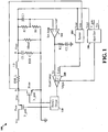
- FIG. 1 is a schematic diagram of a voltage regulator 100 that implements a buck converter.
- the voltage regulator 100 receives an input voltage Vin and generates an output voltage Vout for a load Rload.
- the voltage regulator 100 includes a first switch P-sw and a second switch N-sw that operate to provide a switch voltage Vsw at node A. Details of switch operation are provided below.
- the voltage regulator 102 further includes an inductor L0, two resistors ESR_L and ESR_C and a capacitor C0.
- the inductor L0 has one end coupled to node A through the resistor ESR_L and the other end coupled to a node B.
- the capacitor C0 has one end coupled to node B and the other end coupled to circuit ground.
- the inductor L0 and capacitor C0 filter the switch voltage Vsw at node A to generate the output voltage Vout at node B.
- the inductor 120 and capacitor 130 may be of suitable values to provide the desired amount of filtering for Vout.
- the output voltage Vout passes through a voltage divider formed by resistors R1 and R0 and capacitor C1 and is input to an error amplifier 102 at a non-inverting input.
- a reference voltage Vref is also input to the error amplifier 102 at an inverting input.
- the reference voltage Vref is a target voltage for Vout and may be a fixed value or a configurable value.
- the error amplifier 102 compares the two voltages to obtain an error, amplifies the error, and provides an amplified error signal Ve.
- the resistor R2 and capacitor C2 at the output of the error amplifier 102 provide filtering and frequency compensation.
- the voltage regulator 100 also includes a current sense 104, a hysteresis generator 106, and hysteresis comparator 108 and a switch driver controller 110.
- the current sense 104 obtains the voltage across the inductor L0 through the voltage Vout on a first end of the inductor 120 and the switch voltage Vsw on the second side of the inductor L0, and senses the current through the inductor.
- the current sense 104 outputs a voltage sense Visns derived from the sensed current.
- the hysteresis generator 106 receives the voltage Vout, a signal that drives the first switch P-sw and the input voltage Vin.
- the circuitry of the hysteresis generator 106 generates a hysteresis parameter, which may be a hysteresis voltage Vhyst or a hysteresis current Ihyst.
- the hysteresis parameter used further herein is a hysteresis voltage Vhyst.
- the hysteresis generator 106 is configured to provide a hysteresis parameter that allows the voltage regulator 102 to operate in a relatively constant frequency.
- the hysteresis comparator 108 receives the amplified error signal Ve from the error amplifier 102, the voltage sense Visns from the current sense 104, and the hysteresis voltage Vhyst from the hysteresis generator 106 and generates control signals for the first and second switches P-sw, N-sw.
- the hysteresis comparator 108 may include two comparators. A first comparator compares a summation of the amplified error signal Ve and the voltage hysteresis Vhyst to the voltage sense Visns and outputs a first signal Sp. A second comparator compares a difference of the amplified error signal Ve and the voltage hysteresis Vhyst to the voltage sense Visns and outputs a second signal.
- the first and second output signals of the hysteresis comparator 108 are input to the switch driver controller 110 and output respectively as switch control signals Sp and Sn.
- Switch control signal Sp drives the P gate of the first switch P-sw
- switch control signal Sn drives the N gate of the second switch N-sw.
- the first switch P-sw may be a P-channel power field effect transistor (FET) switch with its source coupled to the input voltage Vin, its gate receiving the Sp control signal, and its drain coupled to node A.
- the second switch Sn may be an N-channel FET switch with its drain coupled to the node A, its gate receiving the Sn signal, and its source coupled to circuit ground.
- the first switch P-sw is turned on when the Sp signal is at logic low, and the second switch N-sw is turned on when the Sn signal is at logic high.
- the Sp and Sn control signals may be generated such that at most one switch is turned on at any given moment.
- the first and second switches provide the switch voltage Vsw output signal at node A. This output signal is a square wave signal that swings from Vin to circuit ground and has a duty cycle determined by Vout.
- the majority of the voltage regulator 100 may be fabricated on an integrated power management circuit (IC), with several circuit components remaining external to the IC ship.
- IC integrated power management circuit
- the inductor L0, two resistors ESR_L, ESR_C and Rload, and the capacitor C0 are external to the power management IC.
- the voltage regulator 102 operates as follows. During an On state, the first switch P-sw is turned on by the Sp signal, and the second switch N-sw is turned off by the Sn signal. The input voltage Vin is coupled via the first switch P-sw to the inductor L0, which stores energy from the Vin supply voltage. The current through the inductor L0 rises during the On state, with the rate of the rise being dependent on the difference between Vin and Vout and the inductance L of the inductor L0. During an Off state, the first switch P-sw is turned off by the Sp signal, and the Vin supply voltage is disconnected from the inductor L0.
- the second switch N-sw is turned on by the Sn signal, and the inductor L0 is coupled between circuit ground and node B.
- the current through the inductor L0 falls during the Off state, with the rate of the fall being dependent on the output voltage Vout and the inductance L.
- the input voltage Vin thus provides current to the capacitor C0 and the load Rload during the On state, and the inductor L0 provides its stored energy to the capacitor C0 and load Rload during the Off state.
- the capacitor C0 maintains the output voltage Vout at node B and also provides its charge to load Rload during the Off state.
- the duty cycle is the percentage of time that the buck converter is in the On state.
- the output voltage Vout may be varied by adjusting the duty cycle of the switch control signals Sp and Sn for the switches P-sw and N-sw.
- the first switch P-sw When the output voltage Vout is below Vref, the first switch P-sw may be turned on longer to bring up the output voltage Vout. Conversely, when the output voltage Vout is above Vref, the first switch P-sw may be turned on shorter to bring down the output voltage Vout.
- the inductor L0 and capacitor C0 provide filtering for the regulator output signal at node A.
- a larger inductor L0 and/or a larger capacitor C0 may provide more filtering, which may reduce the magnitude of ripples on the voltage output Vout at node B.
- the sizes of inductor L0 and capacitor C0 may be selected based on a tradeoff between the amount of ripple, cost, and area.
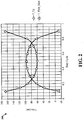
- the curve T_Td represents changes in the time period T of the voltage regulator as a function of duty cycle that are due to the inherent loop delay Td of the voltage regulator.
- T_Td is a function of the inherent loop delay Td and the duty cycle D.
- the curve T_Td indicates a minimum time delay Td, and thus a minimum affect on time period T, when the duty cycle is close to .5.
- the time delay Td, and thus the affect on time period T increases non-linearly on both sides as the duty cycle changes.
- the presence of the inherent time delay Td causes the time period T of the voltage regulator to vary significantly as a function of duty cycle.
- Buck regulators work at very different duty cycles, preferably while maintaining a substantially constant time period T.
- the voltage regulator disclosed herein provides a hysteresis time period T_hyst that compensates for the varying time period corresponding to the curve T_Td.
- the T_hyst curve illustrated in FIG. 2 is essentially an inverse of the curve T_Td. A combination of the two curve results in a substantially fixed operating frequency, i.e., fixed switching time period T.
- the hysteresis time period T_hyst is derived from circuit elements within the hysteresis generator 106 of FIG. 1 . These circuit elements are the same elements that provide the hysteresis parameter V_hyst to the hysteresis comparator 108.
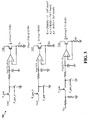
- FIG. 3 is a schematic of the hysteretic generator 106.
- the hysteretic generator has the following set of inputs: a voltage output Vout of the buck regulator, a voltage input Vin of the buck regulator, and a signal that drives a P gate switch of the buck regulator.
- the hysteretic generator 106 includes first, second and third circuits 302, 304, 306, which provide measures of a first current I1, a second current I2 and a third current I3, respectively.
- Each circuit 302, 303, 304 includes a pair of switches P_gate and P_gate_b that operate in accordance with switch P-sw of the voltage regulator. More specifically, when the switch P-sw of the voltage regulator is closed, the P-gate switches of the circuits 302, 304, 306 are closed and the P_gate_b switches are open. Conversely, when the switch P-sw of the voltage regulator is opened, the P-gate switches of the circuits 302, 304, 306 are opened and the P_gate_b switches are closed.
- the first circuit 302 receives output voltage Vout and provides a voltage Vout x (1-D) to an input of an amplifier when the P-gate is closed.
- the voltage is output by the amplifier to a gate of a FET.
- the second circuit 304 receives output voltage Vout and provides a voltage Vout x (D) to an input of an amplifier when the P-gate is closed.
- the voltage is output by the amplifier to a gate of a FET.
- Vhyst 2 * I 1 ⁇ I 2 ⁇ I 3 * R 4 where resistance R4 (not shown) is provided by a fourth resistor (not shown) through which the summation of currents (I1, I2, I3) pass.
- the hysteresis parameter Vhyst is provided to the hysteresis comparator 108 for use in controlling the switches P-sw and N-sw of the voltage regulator.
- the circuitry of the hysteresis generator 106 includes elements selected to provide a hysteresis time period T_hyst, which in combination with the inherent time delay T_Td of the voltage regulator, results in a substantially constant operating period for the voltage regulator, independent of duty cycle changes.
- T_hyst Vhyst * L / Asns * Vout * 1 ⁇ D
- L is the known inductor value for the voltage regulator (e.g., L0 of FIG.
- T_hyst L / Asns * K 1 ⁇ K 2 * D / 1 ⁇ D ⁇ K 3 * 1 / D
- L the known inductor value for the voltage regulator (e.g., L0 of FIG. 1 )
- Asns is a current sense gain based on a voltage sensed across the inductor L and a current through the inductor
- D Vout/Vin
- K1 2*R4/R1
- K2 2* R4/R2
- K3 R4/R3.
- T T_Td + T_hyst
- This time period T is independent of duty cycle D.
- the hysteresis generator and the circuitry therein provide a hysteresis parameter that controls the switch of the buck regulator so that the regulator maintains a substantially constant switching time period.
- FIG. 4 is a flow chart 400 of a method of operating a voltage regulator having a plurality of switches and a delay time period T_Td.
- the method may be performed by one or more components of the voltage regulator, including for example, a hysteresis generator, a hysteresis comparator, and a switch driver.
- a hysteresis generator provides a hysteresis parameter V_hyst to a hysteresis comparator.
- the hysteresis parameter V_hyst is a function of circuit components, a voltage output Vout of the regulator, a voltage input Vin of the regulator, and a signal that drives one of the plurality of switches.
- a switch driver drives the switches based on the hysteresis parameter.
- One or more of the circuit components that provide the hysteresis parameter also define a hysteresis time period T_ hyst.
- the hysteresis time period T_ hyst defines in combination with the delay time period T_Td, a switching time period T for the regulator that is substantially constant.
- the circuit components that provide the hysteresis parameter for the switch driver include a first resistor having a resistance R1, a second resistor having a resistance R2, a third resistor having a resistance R3, and a fourth resistor having a resistance R4.
- L is the inductance of an inductor of the regulator
- Asns is based on a voltage sensed across the inductor and a current through the inductor
- D Vout/Vin.
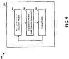
- FIG. 5 is a high level signal flow diagram 500 illustrating the signal flow between different modules/means/components in an exemplary voltage regulator 502.
- the regulator 502 includes a hysteresis parameter generator module 504, a switch driver module 506 that includes a hysteresis comparator, and a switch module 508 that includes a plurality of switches.
- the modules of the voltage regulator 502 perform each of the steps of the process in the aforementioned flow chart of FIG. 4 .
- the modules may be one or more hardware components specifically configured to carry out the stated steps.
- the hysteresis parameter generator module 504 provides a hysteresis parameter V_hyst to the hysteresis comparator of the switch drive module 506.
- the hysteresis parameter V_hyst is a function of circuit components of the hysteresis parameter generator module, a voltage output Vout of the regulator, a voltage input Vin of the regulator, and a signal that drives one of the plurality of switches in the switch module 508.
- the circuit components of the hysteresis parameter generator module 504 may include components of FIG. 3 .
- the switch driver module 506 drives the switches of the switch module 508 based on the output of the hysteresis comparator, whose output is based on the hysteresis parameter provided by the hysteresis parameter generator module 504.
- One or more of the circuit components that provide the hysteresis parameter also define a hysteresis time period T_ hyst.
- the hysteresis time period T_ hyst defines in combination with the delay time period T_Td, a switching time period T for the regulator that is substantially constant.
- the switch driver module 506 may include the hysteresis comparator 108 and switch driver 110 of FIG. 1
- the switch module 508 receives switch control signals from the switch driver module 506 and operates in accordance with the switch signal.
- the switch module 508 may include the switch P-sw and switch N-sw of FIG. 1 .
- the voltage regulator 502 includes means for providing a hysteresis parameter V_hyst to a hysteresis comparator, the hysteresis parameter V_hyst being a function of circuit components, a voltage output Vout of the regulator, a voltage input Vin of the regulator, and a signal that drives one of the plurality of switches.
- the voltage regulator also includes means for driving a plurality of switches based on the hysteresis parameter, wherein one or more of the circuit components that provide the hysteresis parameter also define a hysteresis time period T_ hyst.
- the hysteresis time period T_ hyst defines in combination with a delay time period T_Td of the regulator, a switching time period T for the regulator that is substantially constant.
- the aforementioned means may be one or more of the aforementioned modules of the voltage regulator 502.
- FIG. 6 shows a block diagram of a design of a wireless communication device 600.
- Wireless device 600 may be a cellular phone, a terminal, a handset, a personal digital assistant (PDA), etc.
- Wireless device 600 may be capable of communicating with one or more wireless communication systems such as a Code Division Multiple Access (CDMA) system, a Global System for Mobile Communications (GSM) system, a wireless local area network (WLAN), etc.
- CDMA Code Division Multiple Access
- GSM Global System for Mobile Communications
- WLAN wireless local area network
- Wireless device 600 is capable of providing bi-directional communication via a transmit path and a receive path.
- a transmitter (TMTR) 614 receives data from an application specific integrated circuit (ASIC) 620, processes and conditions the data, and generates a modulated signal, which is transmitted via an antenna 612 to base stations.
- ASIC application specific integrated circuit
- RCVR receiver
- Receiver 616 conditions and digitizes the received signal and provides samples to ASIC 620 for further processing.
- ASIC 620 may include various processing, interface and memory units such as, e.g., a modem processor 622, a controller/processor 624, an internal memory 626, a reduced instruction set computing (RISC) processor 628, an external bus interface (EBI) 630, and a serial bus interface (SBI) 632.
- Modem processor 622 may perform processing for data transmission and reception, e.g., encoding, modulation, demodulation, decoding, etc.
- RISC processor 628 may perform various types of processing for wireless device 600, e.g., processing for video, graphics, higher layer applications, etc.
- Controller/processor 624 may direct the operation of various units within ASIC 620.
- Internal memory 626 may store data and/or instructions for various units within ASIC 620.
- External bus interface 630 may facilitate transfer of data between ASIC 620 and a main memory 640, which may provide bulk storage for data and program codes used by ASIC 620.
- Serial bus interface 632 may facilitate communication between ASIC 620 and an ASIC 650.
- ASIC 650 may include various circuit blocks such as, e.g., an audio driver 652, a video driver 654, an input/output (I/O) driver 656, and a power controller 660.
- Audio driver 652 may drive an audio device 662.
- Video driver 654 may drive a display unit 664.
- I/O, driver 656 may drive an I/O device 666.
- Power controller 660 may couple to an external battery 670 and/or receive external power via a power convector. Power controller 660 may generate output voltages for the processing units within ASIC 620.
- Power controller 660 may implement any of the designs shown in FIGS. 2A, 2B , 3 and 6 .
- ASIC 620 may be partitioned into multiple power domains in order to facilitate powering down in idle mode. Each power domain may include circuit blocks coupled to a respective output voltage and may correspond to one load 660 in FIG. 6 .
- ASIC 620 may be a Mobile Station Modem (MSM) from Qualcomm Incorporated.
- ASIC 650 may be a Power Management IC (PMIC) from Qualcomm Incorporated.
- ASICs 620 and 650 may also be other ICs from other manufacturers.
- ASICs 620 and 650 may each comprise a single IC die or multiple IC dies.
- the voltage regulator with transient recovery circuits described herein may be implemented on an IC, an analog IC, a radio frequency IC (RFIC), a mixed-signal IC, an ASIC, a printed circuit board (PCB), an electronics device, etc.
- the voltage regulator with transient recovery circuits may also be fabricated with various IC process technologies such as complementary metal oxide semiconductor (CMOS), N-channel MOS (NMOS), P-channel MOS (PMOS), bipolar junction transistor (BJT), bipolar-CMOS (BiCMOS), silicon germanium (SiGe), gallium arsenide (GaAs), etc.
- CMOS complementary metal oxide semiconductor
- NMOS N-channel MOS
- PMOS P-channel MOS
- BJT bipolar junction transistor
- BiCMOS bipolar-CMOS
- SiGe silicon germanium
- GaAs gallium arsenide
- An apparatus implementing the voltage regulator with transient recovery circuits described herein may be a stand-alone device or may be part of a larger device.
- a device may be (i) a stand-alone IC, (ii) a set of one or more ICs that may include memory ICs for storing data and/or instructions, (iii) an RFIC such as an RF receiver (RFR) or an RF transmitter/receiver (RTR), (iv) an ASIC such as an MSM, (v) a module that may be embedded within other devices, (vi) a receiver, cellular phone, wireless device, handset, or mobile unit, (vii) etc.
- RFR RF receiver
- RTR RF transmitter/receiver
- the functions described may be implemented in hardware, software, firmware, or any combination thereof. If implemented in software, the functions may be stored on or transmitted over as one or more instructions or code on a computer-readable medium.
- Computer-readable media includes both computer storage media and communication media including any medium that facilitates transfer of a computer program from one place to another.
- a storage media may be any available media that can be accessed by a computer.
- such computer-readable media can comprise RAM, ROM, EEPROM, CD-ROM or other optical disk storage, magnetic disk storage or other magnetic storage devices, or any other medium that can be used to carry or store desired program code in the form of instructions or data structures and that can be accessed by a computer.
- any connection is properly termed a computer-readable medium.
- the software is transmitted from a website, server, or other remote source using a coaxial cable, fiber optic cable, twisted pair, digital subscriber line (DSL), or wireless technologies such as infrared, radio, and microwave
- the coaxial cable, fiber optic cable, twisted pair, DSL, or wireless technologies such as infrared, radio, and microwave are included in the definition of medium.
- Disk and disc includes compact disc (CD), laser disc, optical disc, digital versatile disc (DVD), floppy disk and blu-ray disc where disks usually reproduce data magnetically, while discs reproduce data optically with lasers. Combinations of the above should also be included within the scope of computer-readable media.
Landscapes
- Engineering & Computer Science (AREA)
- Power Engineering (AREA)
- Dc-Dc Converters (AREA)
- Ac-Ac Conversion (AREA)
- General Induction Heating (AREA)
Priority Applications (2)
| Application Number | Priority Date | Filing Date | Title |
|---|---|---|---|
| SM20170381T SMT201700381T1 (it) | 2013-03-08 | 2014-03-04 | Metodo di controllo di frequenza a reazione positiva per un regolatore abbassatore di tensione a isteresi a modo di corrente |
| HRP20170859TT HRP20170859T1 (hr) | 2013-03-08 | 2014-03-04 | Metoda za unaprijedno vođenje frekvencije za strujni režim histereznog silaznog regulatora |
Applications Claiming Priority (2)
| Application Number | Priority Date | Filing Date | Title |
|---|---|---|---|
| US13/791,868 US9264033B2 (en) | 2013-03-08 | 2013-03-08 | Feed-forward frequency control method for current mode hysteretic buck regulator |
| PCT/US2014/020424 WO2014138130A1 (en) | 2013-03-08 | 2014-03-04 | Feed-forward frequency control method for current mode hysteretic buck regulator |
Publications (2)
| Publication Number | Publication Date |
|---|---|
| EP2965414A1 EP2965414A1 (en) | 2016-01-13 |
| EP2965414B1 true EP2965414B1 (en) | 2017-04-19 |
Family
ID=50440810
Family Applications (1)
| Application Number | Title | Priority Date | Filing Date |
|---|---|---|---|
| EP14715731.7A Active EP2965414B1 (en) | 2013-03-08 | 2014-03-04 | Feed-forward frequency control method for current mode hysteretic buck regulator |
Country Status (8)
Families Citing this family (8)
| Publication number | Priority date | Publication date | Assignee | Title |
|---|---|---|---|---|
| JP6097237B2 (ja) * | 2014-03-10 | 2017-03-15 | 株式会社東芝 | Dc−dcコンバータおよび半導体集積回路 |
| EP3261241B1 (en) * | 2016-06-20 | 2019-01-30 | NXP USA, Inc. | Switched current control module and method therefor |
| US10236773B2 (en) * | 2016-09-30 | 2019-03-19 | Cypress Semiconductor Corporation | Low quiescent current DC-to-DC converter with increased output voltage accuracy |
| DE102017111006B4 (de) | 2017-05-19 | 2021-06-24 | Infineon Technologies Austria Ag | Leistungswandlerschaltung mit einem getakteten Leistungswandler |
| EP3631963B1 (en) | 2017-05-31 | 2022-03-23 | Intuitive Surgical Operations, Inc. | Electrosurgical output stage with integrated dc regulator |
| JP2019092010A (ja) * | 2017-11-13 | 2019-06-13 | 株式会社東海理化電機製作所 | 信号処理装置 |
| CN110880926B (zh) * | 2018-09-05 | 2023-07-28 | 欧姆龙株式会社 | 开关驱动电路以及电气设备 |
| CN114649935B (zh) * | 2020-12-17 | 2024-08-30 | 圣邦微电子(北京)股份有限公司 | 开关变换器及其控制电路 |
Family Cites Families (11)
| Publication number | Priority date | Publication date | Assignee | Title |
|---|---|---|---|---|
| JPH09135568A (ja) * | 1995-11-07 | 1997-05-20 | Toyota Autom Loom Works Ltd | Dc/dcコンバータ |
| US6885175B2 (en) * | 2002-10-25 | 2005-04-26 | International Rectifier Corporation | Fixed frequency hysteretic regulator |
| JP4479358B2 (ja) * | 2004-06-07 | 2010-06-09 | 株式会社村田製作所 | Dc−dcコンバータ |
| US7423414B1 (en) * | 2005-08-04 | 2008-09-09 | National Semiconductor Corporation | Apparatus and method for switching regulator with compensation delay for output voltage error correction |
| US8008902B2 (en) * | 2008-06-25 | 2011-08-30 | Cirrus Logic, Inc. | Hysteretic buck converter having dynamic thresholds |
| EP2308162A1 (en) | 2008-07-28 | 2011-04-13 | Nxp B.V. | Delay compensation for a dc-dc converter |
| US8169205B2 (en) | 2009-05-26 | 2012-05-01 | Silergy Technology | Control for regulator fast transient response and low EMI noise |
| CN102315773B (zh) * | 2010-07-02 | 2014-02-12 | 成都芯源系统有限公司 | 一种开关变换器的装置和方法 |
| US8164391B2 (en) * | 2010-07-28 | 2012-04-24 | Active-Semi, Inc. | Synchronization of multiple high frequency switching power converters in an integrated circuit |
| US8269423B2 (en) * | 2010-09-10 | 2012-09-18 | Monolithic Power Systems, Inc. | LED drivers with adaptive hysteretic control circuits and associated methods of operation |
| US8884592B2 (en) | 2011-08-26 | 2014-11-11 | Broadcom Corporation | Frequency lock loop for hysteretic switching regulators |
-
2013
- 2013-03-08 US US13/791,868 patent/US9264033B2/en not_active Expired - Fee Related
-
2014
- 2014-03-04 KR KR1020157027135A patent/KR20150127146A/ko not_active Withdrawn
- 2014-03-04 WO PCT/US2014/020424 patent/WO2014138130A1/en active Application Filing
- 2014-03-04 EP EP14715731.7A patent/EP2965414B1/en active Active
- 2014-03-04 SM SM20170381T patent/SMT201700381T1/it unknown
- 2014-03-04 JP JP2015561564A patent/JP6377085B2/ja not_active Expired - Fee Related
- 2014-03-04 CN CN201480012395.5A patent/CN105009435B/zh not_active Expired - Fee Related
- 2014-03-04 HR HRP20170859TT patent/HRP20170859T1/hr unknown
Non-Patent Citations (1)
| Title |
|---|
| None * |
Also Published As
| Publication number | Publication date |
|---|---|
| KR20150127146A (ko) | 2015-11-16 |
| HRP20170859T1 (hr) | 2017-12-01 |
| JP2016509469A (ja) | 2016-03-24 |
| WO2014138130A1 (en) | 2014-09-12 |
| SMT201700381T1 (it) | 2017-09-07 |
| JP6377085B2 (ja) | 2018-08-22 |
| CN105009435B (zh) | 2018-02-02 |
| US9264033B2 (en) | 2016-02-16 |
| EP2965414A1 (en) | 2016-01-13 |
| US20140253181A1 (en) | 2014-09-11 |
| CN105009435A (zh) | 2015-10-28 |
Similar Documents
| Publication | Publication Date | Title |
|---|---|---|
| EP2965414B1 (en) | Feed-forward frequency control method for current mode hysteretic buck regulator | |
| US20090237854A1 (en) | Voltage regulator with transient recovery circuit | |
| US11444537B2 (en) | Power converters and compensation circuits thereof | |
| US8928303B2 (en) | Apparatus and methods for transient compensation of switching power regulators | |
| US20210067033A1 (en) | Differential sensing and maintenance of flying capacitor voltage in a switched-mode power supply circuit | |
| TW202241031A (zh) | 在自我調整組合電源電路中在降壓變換器模式和電荷泵模式之間的基於電流的轉換 | |
| US9225234B2 (en) | In-rush current control for charge-pump LDO | |
| US9148052B2 (en) | Switching regulator with reduced EMI | |
| GB2472114A (en) | Switched power regulator having estimated error signal | |
| WO2015138189A1 (en) | Average current mode control of multi-phase switching power converters | |
| US11171493B2 (en) | Wireless parallel charging | |
| US9595866B2 (en) | Hysteretic switching regulator including a power converting unit and a switch driving unit | |
| US20140292298A1 (en) | Operational Amplifier-Based Current-Sensing Circuit for DC-DC Voltage Converters and The Like | |
| US10333393B2 (en) | Embedded charge pump voltage regulator | |
| US20210194365A1 (en) | Frequency limit circuit and dc-dc converter including the same | |
| US8339164B2 (en) | Antenna driving device | |
| CN111108674B (zh) | 多相转换器中的自动相电流平衡 | |
| Ma et al. | A high efficiency adaptive current mode step-up/step-down DC–DC converter with four modes for smooth transition | |
| US20210036617A1 (en) | Methods and apparatuses for a multi-mode regulator architecture | |
| Wong et al. | Design of a fast-transient current-mode buck DC-DC converter | |
| Keskar et al. | One Clock‐Cycle Response 0.5 μm CMOS Dual‐Mode ΣΔ DC‐DC Bypass Boost Converter Stable over Wide RESRLC Variations |
Legal Events
| Date | Code | Title | Description |
|---|---|---|---|
| PUAI | Public reference made under article 153(3) epc to a published international application that has entered the european phase |
Free format text: ORIGINAL CODE: 0009012 |
|
| 17P | Request for examination filed |
Effective date: 20150807 |
|
| AK | Designated contracting states |
Kind code of ref document: A1 Designated state(s): AL AT BE BG CH CY CZ DE DK EE ES FI FR GB GR HR HU IE IS IT LI LT LU LV MC MK MT NL NO PL PT RO RS SE SI SK SM TR |
|
| AX | Request for extension of the european patent |
Extension state: BA ME |
|
| DAX | Request for extension of the european patent (deleted) | ||
| GRAP | Despatch of communication of intention to grant a patent |
Free format text: ORIGINAL CODE: EPIDOSNIGR1 |
|
| INTG | Intention to grant announced |
Effective date: 20160913 |
|
| STAA | Information on the status of an ep patent application or granted ep patent |
Free format text: STATUS: GRANT OF PATENT IS INTENDED |
|
| GRAS | Grant fee paid |
Free format text: ORIGINAL CODE: EPIDOSNIGR3 |
|
| GRAA | (expected) grant |
Free format text: ORIGINAL CODE: 0009210 |
|
| STAA | Information on the status of an ep patent application or granted ep patent |
Free format text: STATUS: THE PATENT HAS BEEN GRANTED |
|
| AK | Designated contracting states |
Kind code of ref document: B1 Designated state(s): AL AT BE BG CH CY CZ DE DK EE ES FI FR GB GR HR HU IE IS IT LI LT LU LV MC MK MT NL NO PL PT RO RS SE SI SK SM TR |
|
| REG | Reference to a national code |
Ref country code: GB Ref legal event code: FG4D |
|
| REG | Reference to a national code |
Ref country code: CH Ref legal event code: EP |
|
| REG | Reference to a national code |
Ref country code: AT Ref legal event code: REF Ref document number: 886806 Country of ref document: AT Kind code of ref document: T Effective date: 20170515 |
|
| REG | Reference to a national code |
Ref country code: IE Ref legal event code: FG4D |
|
| REG | Reference to a national code |
Ref country code: DE Ref legal event code: R096 Ref document number: 602014008806 Country of ref document: DE |
|
| REG | Reference to a national code |
Ref country code: HR Ref legal event code: TUEP Ref document number: P20170859 Country of ref document: HR |
|
| REG | Reference to a national code |
Ref country code: EE Ref legal event code: FG4A Ref document number: E013977 Country of ref document: EE Effective date: 20170619 |
|
| REG | Reference to a national code |
Ref country code: NL Ref legal event code: MP Effective date: 20170419 |
|
| REG | Reference to a national code |
Ref country code: LT Ref legal event code: MG4D |
|
| REG | Reference to a national code |
Ref country code: AT Ref legal event code: MK05 Ref document number: 886806 Country of ref document: AT Kind code of ref document: T Effective date: 20170419 |
|
| PG25 | Lapsed in a contracting state [announced via postgrant information from national office to epo] |
Ref country code: NL Free format text: LAPSE BECAUSE OF FAILURE TO SUBMIT A TRANSLATION OF THE DESCRIPTION OR TO PAY THE FEE WITHIN THE PRESCRIBED TIME-LIMIT Effective date: 20170419 |
|
| PG25 | Lapsed in a contracting state [announced via postgrant information from national office to epo] |
Ref country code: AT Free format text: LAPSE BECAUSE OF FAILURE TO SUBMIT A TRANSLATION OF THE DESCRIPTION OR TO PAY THE FEE WITHIN THE PRESCRIBED TIME-LIMIT Effective date: 20170419 Ref country code: ES Free format text: LAPSE BECAUSE OF FAILURE TO SUBMIT A TRANSLATION OF THE DESCRIPTION OR TO PAY THE FEE WITHIN THE PRESCRIBED TIME-LIMIT Effective date: 20170419 Ref country code: NO Free format text: LAPSE BECAUSE OF FAILURE TO SUBMIT A TRANSLATION OF THE DESCRIPTION OR TO PAY THE FEE WITHIN THE PRESCRIBED TIME-LIMIT Effective date: 20170719 Ref country code: GR Free format text: LAPSE BECAUSE OF FAILURE TO SUBMIT A TRANSLATION OF THE DESCRIPTION OR TO PAY THE FEE WITHIN THE PRESCRIBED TIME-LIMIT Effective date: 20170720 Ref country code: FI Free format text: LAPSE BECAUSE OF FAILURE TO SUBMIT A TRANSLATION OF THE DESCRIPTION OR TO PAY THE FEE WITHIN THE PRESCRIBED TIME-LIMIT Effective date: 20170419 Ref country code: LT Free format text: LAPSE BECAUSE OF FAILURE TO SUBMIT A TRANSLATION OF THE DESCRIPTION OR TO PAY THE FEE WITHIN THE PRESCRIBED TIME-LIMIT Effective date: 20170419 |
|
| PG25 | Lapsed in a contracting state [announced via postgrant information from national office to epo] |
Ref country code: LV Free format text: LAPSE BECAUSE OF FAILURE TO SUBMIT A TRANSLATION OF THE DESCRIPTION OR TO PAY THE FEE WITHIN THE PRESCRIBED TIME-LIMIT Effective date: 20170419 Ref country code: BG Free format text: LAPSE BECAUSE OF FAILURE TO SUBMIT A TRANSLATION OF THE DESCRIPTION OR TO PAY THE FEE WITHIN THE PRESCRIBED TIME-LIMIT Effective date: 20170719 Ref country code: SE Free format text: LAPSE BECAUSE OF FAILURE TO SUBMIT A TRANSLATION OF THE DESCRIPTION OR TO PAY THE FEE WITHIN THE PRESCRIBED TIME-LIMIT Effective date: 20170419 Ref country code: RS Free format text: LAPSE BECAUSE OF FAILURE TO SUBMIT A TRANSLATION OF THE DESCRIPTION OR TO PAY THE FEE WITHIN THE PRESCRIBED TIME-LIMIT Effective date: 20170419 Ref country code: PL Free format text: LAPSE BECAUSE OF FAILURE TO SUBMIT A TRANSLATION OF THE DESCRIPTION OR TO PAY THE FEE WITHIN THE PRESCRIBED TIME-LIMIT Effective date: 20170419 |
|
| REG | Reference to a national code |
Ref country code: HR Ref legal event code: T1PR Ref document number: P20170859 Country of ref document: HR |
|
| REG | Reference to a national code |
Ref country code: SK Ref legal event code: T3 Ref document number: E 24875 Country of ref document: SK |
|
| REG | Reference to a national code |
Ref country code: DE Ref legal event code: R097 Ref document number: 602014008806 Country of ref document: DE |
|
| PG25 | Lapsed in a contracting state [announced via postgrant information from national office to epo] |
Ref country code: DK Free format text: LAPSE BECAUSE OF FAILURE TO SUBMIT A TRANSLATION OF THE DESCRIPTION OR TO PAY THE FEE WITHIN THE PRESCRIBED TIME-LIMIT Effective date: 20170419 Ref country code: RO Free format text: LAPSE BECAUSE OF FAILURE TO SUBMIT A TRANSLATION OF THE DESCRIPTION OR TO PAY THE FEE WITHIN THE PRESCRIBED TIME-LIMIT Effective date: 20170419 Ref country code: CZ Free format text: LAPSE BECAUSE OF FAILURE TO SUBMIT A TRANSLATION OF THE DESCRIPTION OR TO PAY THE FEE WITHIN THE PRESCRIBED TIME-LIMIT Effective date: 20170419 |
|
| PLBE | No opposition filed within time limit |
Free format text: ORIGINAL CODE: 0009261 |
|
| REG | Reference to a national code |
Ref country code: FR Ref legal event code: PLFP Year of fee payment: 5 |
|
| STAA | Information on the status of an ep patent application or granted ep patent |
Free format text: STATUS: NO OPPOSITION FILED WITHIN TIME LIMIT |
|
| 26N | No opposition filed |
Effective date: 20180122 |
|
| PG25 | Lapsed in a contracting state [announced via postgrant information from national office to epo] |
Ref country code: SI Free format text: LAPSE BECAUSE OF FAILURE TO SUBMIT A TRANSLATION OF THE DESCRIPTION OR TO PAY THE FEE WITHIN THE PRESCRIBED TIME-LIMIT Effective date: 20170419 |
|
| PGFP | Annual fee paid to national office [announced via postgrant information from national office to epo] |
Ref country code: IT Payment date: 20180315 Year of fee payment: 5 |
|
| REG | Reference to a national code |
Ref country code: CH Ref legal event code: PL |
|
| PG25 | Lapsed in a contracting state [announced via postgrant information from national office to epo] |
Ref country code: MC Free format text: LAPSE BECAUSE OF FAILURE TO SUBMIT A TRANSLATION OF THE DESCRIPTION OR TO PAY THE FEE WITHIN THE PRESCRIBED TIME-LIMIT Effective date: 20170419 |
|
| REG | Reference to a national code |
Ref country code: BE Ref legal event code: MM Effective date: 20180331 |
|
| REG | Reference to a national code |
Ref country code: IE Ref legal event code: MM4A |
|
| PG25 | Lapsed in a contracting state [announced via postgrant information from national office to epo] |
Ref country code: LU Free format text: LAPSE BECAUSE OF NON-PAYMENT OF DUE FEES Effective date: 20180304 |
|
| PG25 | Lapsed in a contracting state [announced via postgrant information from national office to epo] |
Ref country code: IE Free format text: LAPSE BECAUSE OF NON-PAYMENT OF DUE FEES Effective date: 20180304 |
|
| PG25 | Lapsed in a contracting state [announced via postgrant information from national office to epo] |
Ref country code: BE Free format text: LAPSE BECAUSE OF NON-PAYMENT OF DUE FEES Effective date: 20180331 Ref country code: CH Free format text: LAPSE BECAUSE OF NON-PAYMENT OF DUE FEES Effective date: 20180331 Ref country code: LI Free format text: LAPSE BECAUSE OF NON-PAYMENT OF DUE FEES Effective date: 20180331 |
|
| REG | Reference to a national code |
Ref country code: HR Ref legal event code: ODRP Ref document number: P20170859 Country of ref document: HR Payment date: 20190227 Year of fee payment: 6 |
|
| PG25 | Lapsed in a contracting state [announced via postgrant information from national office to epo] |
Ref country code: IT Free format text: LAPSE BECAUSE OF NON-PAYMENT OF DUE FEES Effective date: 20190304 |
|
| REG | Reference to a national code |
Ref country code: HR Ref legal event code: ODRP Ref document number: P20170859 Country of ref document: HR Payment date: 20200224 Year of fee payment: 7 |
|
| PG25 | Lapsed in a contracting state [announced via postgrant information from national office to epo] |
Ref country code: TR Free format text: LAPSE BECAUSE OF FAILURE TO SUBMIT A TRANSLATION OF THE DESCRIPTION OR TO PAY THE FEE WITHIN THE PRESCRIBED TIME-LIMIT Effective date: 20170419 |
|
| PGFP | Annual fee paid to national office [announced via postgrant information from national office to epo] |
Ref country code: GB Payment date: 20200228 Year of fee payment: 7 |
|
| PG25 | Lapsed in a contracting state [announced via postgrant information from national office to epo] |
Ref country code: PT Free format text: LAPSE BECAUSE OF FAILURE TO SUBMIT A TRANSLATION OF THE DESCRIPTION OR TO PAY THE FEE WITHIN THE PRESCRIBED TIME-LIMIT Effective date: 20170419 |
|
| PG25 | Lapsed in a contracting state [announced via postgrant information from national office to epo] |
Ref country code: HU Free format text: LAPSE BECAUSE OF FAILURE TO SUBMIT A TRANSLATION OF THE DESCRIPTION OR TO PAY THE FEE WITHIN THE PRESCRIBED TIME-LIMIT; INVALID AB INITIO Effective date: 20140304 Ref country code: CY Free format text: LAPSE BECAUSE OF FAILURE TO SUBMIT A TRANSLATION OF THE DESCRIPTION OR TO PAY THE FEE WITHIN THE PRESCRIBED TIME-LIMIT Effective date: 20170419 |
|
| PGFP | Annual fee paid to national office [announced via postgrant information from national office to epo] |
Ref country code: FR Payment date: 20200219 Year of fee payment: 7 |
|
| PG25 | Lapsed in a contracting state [announced via postgrant information from national office to epo] |
Ref country code: AL Free format text: LAPSE BECAUSE OF FAILURE TO SUBMIT A TRANSLATION OF THE DESCRIPTION OR TO PAY THE FEE WITHIN THE PRESCRIBED TIME-LIMIT Effective date: 20170419 |
|
| REG | Reference to a national code |
Ref country code: DE Ref legal event code: R082 Ref document number: 602014008806 Country of ref document: DE Representative=s name: MAUCHER JENKINS PATENTANWAELTE & RECHTSANWAELT, DE |
|
| REG | Reference to a national code |
Ref country code: HR Ref legal event code: ODRP Ref document number: P20170859 Country of ref document: HR Payment date: 20210218 Year of fee payment: 8 |
|
| GBPC | Gb: european patent ceased through non-payment of renewal fee |
Effective date: 20210304 |
|
| PG25 | Lapsed in a contracting state [announced via postgrant information from national office to epo] |
Ref country code: FR Free format text: LAPSE BECAUSE OF NON-PAYMENT OF DUE FEES Effective date: 20210331 Ref country code: GB Free format text: LAPSE BECAUSE OF NON-PAYMENT OF DUE FEES Effective date: 20210304 |
|
| REG | Reference to a national code |
Ref country code: HR Ref legal event code: ODRP Ref document number: P20170859 Country of ref document: HR Payment date: 20220303 Year of fee payment: 9 |
|
| PGFP | Annual fee paid to national office [announced via postgrant information from national office to epo] |
Ref country code: DE Payment date: 20220210 Year of fee payment: 9 |
|
| REG | Reference to a national code |
Ref country code: HR Ref legal event code: ODRP Ref document number: P20170859 Country of ref document: HR Payment date: 20221230 Year of fee payment: 10 |
|
| REG | Reference to a national code |
Ref country code: DE Ref legal event code: R119 Ref document number: 602014008806 Country of ref document: DE |
|
| PG25 | Lapsed in a contracting state [announced via postgrant information from national office to epo] |
Ref country code: DE Free format text: LAPSE BECAUSE OF NON-PAYMENT OF DUE FEES Effective date: 20231003 |
|
| PGFP | Annual fee paid to national office [announced via postgrant information from national office to epo] |
Ref country code: MK Payment date: 20230210 Year of fee payment: 10 |
|
| REG | Reference to a national code |
Ref country code: HR Ref legal event code: ODRP Ref document number: P20170859 Country of ref document: HR Payment date: 20240219 Year of fee payment: 11 |
|
| PGFP | Annual fee paid to national office [announced via postgrant information from national office to epo] |
Ref country code: SM Payment date: 20241218 Year of fee payment: 12 |
|
| PGFP | Annual fee paid to national office [announced via postgrant information from national office to epo] |
Ref country code: MT Payment date: 20241227 Year of fee payment: 12 |
|
| REG | Reference to a national code |
Ref country code: HR Ref legal event code: ODRP Ref document number: P20170859 Country of ref document: HR Payment date: 20250219 Year of fee payment: 12 |
|
| PGFP | Annual fee paid to national office [announced via postgrant information from national office to epo] |
Ref country code: HR Payment date: 20250219 Year of fee payment: 12 Ref country code: IS Payment date: 20250129 Year of fee payment: 12 |
|
| PGFP | Annual fee paid to national office [announced via postgrant information from national office to epo] |
Ref country code: EE Payment date: 20250210 Year of fee payment: 12 |
|
| PGFP | Annual fee paid to national office [announced via postgrant information from national office to epo] |
Ref country code: SK Payment date: 20250210 Year of fee payment: 12 |