EP2965120B1 - Timestamping detected radiation quanta - Google Patents
Timestamping detected radiation quanta Download PDFInfo
- Publication number
- EP2965120B1 EP2965120B1 EP14709220.9A EP14709220A EP2965120B1 EP 2965120 B1 EP2965120 B1 EP 2965120B1 EP 14709220 A EP14709220 A EP 14709220A EP 2965120 B1 EP2965120 B1 EP 2965120B1
- Authority
- EP
- European Patent Office
- Prior art keywords
- timestamp
- pixel
- optical detector
- unit
- pixel cell
- Prior art date
- Legal status (The legal status is an assumption and is not a legal conclusion. Google has not performed a legal analysis and makes no representation as to the accuracy of the status listed.)
- Active
Links
Images

Classifications
-
- G—PHYSICS
- G01—MEASURING; TESTING
- G01T—MEASUREMENT OF NUCLEAR OR X-RADIATION
- G01T1/00—Measuring X-radiation, gamma radiation, corpuscular radiation, or cosmic radiation
- G01T1/16—Measuring radiation intensity
- G01T1/1606—Measuring radiation intensity with other specified detectors not provided for in the other subgroups of G01T1/16
-
- G—PHYSICS
- G01—MEASURING; TESTING
- G01T—MEASUREMENT OF NUCLEAR OR X-RADIATION
- G01T1/00—Measuring X-radiation, gamma radiation, corpuscular radiation, or cosmic radiation
- G01T1/16—Measuring radiation intensity
- G01T1/17—Circuit arrangements not adapted to a particular type of detector
- G01T1/171—Compensation of dead-time counting losses
-
- G—PHYSICS
- G01—MEASURING; TESTING
- G01T—MEASUREMENT OF NUCLEAR OR X-RADIATION
- G01T1/00—Measuring X-radiation, gamma radiation, corpuscular radiation, or cosmic radiation
- G01T1/16—Measuring radiation intensity
- G01T1/20—Measuring radiation intensity with scintillation detectors
-
- G—PHYSICS
- G01—MEASURING; TESTING
- G01T—MEASUREMENT OF NUCLEAR OR X-RADIATION
- G01T1/00—Measuring X-radiation, gamma radiation, corpuscular radiation, or cosmic radiation
- G01T1/29—Measurement performed on radiation beams, e.g. position or section of the beam; Measurement of spatial distribution of radiation
- G01T1/2914—Measurement of spatial distribution of radiation
- G01T1/2985—In depth localisation, e.g. using positron emitters; Tomographic imaging (longitudinal and transverse section imaging; apparatus for radiation diagnosis sequentially in different planes, steroscopic radiation diagnosis)
Definitions
- the present invention relates to the timestamping of detected radiation quanta and finds application in high energy particle physics applications. Such applications encompass the direct detection of radiation quanta in the form of optical photons such as Cherenkov radiation, as well as the indirect detection of radiation quanta by means of the optical photons produced by a scintillator element.
- the invention finds particular application in PET imaging systems, and even more particularly the invention can be used in time-of-flight (TOF) PET imaging systems.
- TOF time-of-flight
- a radiotracer is administered to a subject such as a patient or an animal prior to its positioning in the PET imaging region.
- the radiotracer is preferentially absorbed by regions in the subject and its distribution is imaged following an uptake period.
- a clinician interprets the relative uptake in particular regions in the images such as organs and may perform a diagnosis of the subject.
- the radiotracer undergoes radioactive decay which results in the production of positrons. Each decay event produces one positron which travels up to a few mm in human tissue where it subsequently interacts with an electron in an annihilation event that produces two oppositely-directed gamma photons.
- the two gamma photons each have an energy of 511 keV and are subsequently detected by gamma photon detectors disposed radially around the PET imaging region which each produce an electrical signal when struck by an incident gamma photon.
- a gamma photon detector defined herein to comprise a scintillator element in optical communication with an optical detector, the scintillator element converts the high energy gamma photon into a scintillation light pulse comprising a number of optical photons, and the electrical signal is generated by the optical detector.
- a timestamp is issued to each electrical signal by a timestamping unit and compared to other timestamps in a coincidence determination unit.
- Two gamma photons are identified as coincident if their timestamps occur within a narrow time interval of each other; typically if they are within +/- 3 ns.
- the positions of the two detectors receiving the coincident gamma photons define a line in space along which the annihilation event occurred, the line being termed a line of response (LOR).
- LOR line of response
- Such LORs are subsequently reconstructed to produce an image illustrative of the distribution of the radiotracer within the imaging region.
- TOF time-of-flight
- PET the small time difference between the two detected gamma photons is further used to localize the position along the LOR at which the annihilation event occurred, and thus improve the spatial resolution of the reconstructed image.
- DOI depth-of-interaction
- PET the trajectories of the two detected gamma photons may further be assessed in order to improve the spatial resolution of the reconstructed image by reducing par
- the timestamping unit that issues timestamps to the received gamma photons typically includes a timing unit such as a time-to-digital converter (TDC), and a timestamp trigger unit.
- the timing unit is caused by the timestamp trigger unit to generate a timestamp indicative of the time of reception of each gamma photon for subsequent analysis by the coincidence determination unit.
- the timestamp trigger unit causes the timing unit to generate a timestamp when a signal at its input exceeds a predetermined threshold and desirably occurs as soon as possible after the detection of the gamma photon in order to optimize the timing accuracy of the PET imaging system.
- a timestamping unit used for timing purposes in the direct detection of radiation quanta such as Cherenkov radiation operates in much the same way.
- the optical detector generates the electrical signal directly from the detected radiation quanta, thus in the absence of a scintillator element.
- False triggering of the timing unit is a problem that can arise in systems employing so-called direct detection, as well as in systems employing indirect detection such as PET imaging systems, and is particularly acute in such which employ digital silicon photomultiplier (SiPM) detectors operating in the Geiger mode as the optical detector.
- SiPM detectors suffer from dark count noise which manifests itself as spurious electrical pulses at the output of the optical detector in the absence of a valid event such as an optical pulse or a received gamma photon.
- the electrical pulses from dark count noise are frequently misinterpreted by the timestamp trigger unit and falsely cause the timing unit to generate a timestamp.
- Timing unit deadtime a period of time during which the timing unit must be reset and during which it is unable to determine the time of reception of valid events.
- Dark count noise is strongly temperature dependent, and even at room temperatures can create considerable timing unit deadtime.
- Some discrimination between dark count noise and the signals from valid events can be achieved by raising the timestamp trigger unit's threshold. This however has limited benefits since the discredited nature of the electrical pulses resulting from both dark count noise and from valid events risks that some valid events do not create a sufficiently large signal to trigger the timestamp trigger unit. The missing of valid events degrades the detection sensitivity. In PET imaging it degrades the system's signal to noise ratio. Raising the timestamp trigger unit's threshold has a further drawback of increasing the time delay between the reception of a valid event and the time of its timestamp, thereby degrading the timing accuracy of the timestamping unit.
- Cooling the optical detector reduces the dark count noise through its temperature dependence and is typically a requirement of such imaging systems. It requires the attachment of bulky cooling apparatus to the optical detectors which adversely impacts system size, cost and power requirements.
- Trigger validation has also been employed in the context of PET imaging. In this, electrical signals from optical detectors responsive to scintillation light pulses resulting from gamma photons are used to generate a trigger validation signal indicative that the trigger signal originated from a gamma photon as opposed to dark count noise.
- a timestamp trigger unit causes a timing unit to generate a timestamp when the first optical photon in the scintillation light pulse has been detected.
- the trigger validation scheme issues a corresponding validity signal based on a logical AND/OR of several such optical detector signals which is true when a predetermined number of such optical detector signals subsequently exceed the threshold.
- a valid trigger of the timing unit consequent to the reception of a gamma photon is characterized by the detection of its scintillation light at multiple optical detectors and causes a true validity signal, resulting in the processing of the timestamp.
- dark count noise triggers fewer optical detectors and causes a false validity signal, resulting in the timestamp being rejected and the timing unit being reset.
- Patent application WO2006/111883A2 discloses a radiation detector that includes an array of detector pixels each including an array of detector cells. Each detector cell includes a photodiode biased in a breakdown region and digital circuitry coupled with the photodiode and configured to output a first digital value in a quiescent state and a second digital value responsive to photon detection by the photodiode. Digital triggering circuitry is configured to output a trigger signal indicative of a start of an integration time period responsive to a selected number of one or more of the detector cells transitioning from the first digital value to the second digital value.
- Patent application US2013/009063A1 discloses a system and method for determining the onset of gamma interactions for PET imaging.
- the timing of a sequence of primary trigger events is obtained and used to determine a weighted combination, which mixes the timing information from the various primary trigger events to compute an overall event trigger timing with improved time resolution.
- Patent application US2013/020487A1 discloses a method of operation of a PET scanner that determines the depth of interaction of the annihilation photons within the scintillator in localizing a temporal photon pair along a line of response (LOR).
- Patent application WO2008/079445A2 discloses a PET apparatus that includes a plurality of radiation sensitive detector systems and selective trigger systems.
- the selective trigger systems identify detector signals resulting from detected gamma radiation while disregarding spurious detector signals.
- the apparatus includes a time to digital converter which decomposes a measurement time interval (T max ) according to a binary hierarchical decomposition of level H, where H is an integer greater than equal to one.
- Patent application US2011/095173A1 discloses a radiation detector that includes a photosensor to receive light via an input and to send an electrical pulse via an output in response to receiving the light.
- the radiation detector can also include a pulse analyzer to send an indicator to a pulse counter when the electrical pulse corresponds to a scintillation pulse and to not send the indicator to the pulse counter when the electrical pulse corresponds to a noise pulse.
- a radiation detection device according to claim 1.
- a system, a method and a computer program product are also disclosed for achieving these objects. Consequently the rejection of noise in the timestamping of detected radiation quanta is improved. In this way the timing unit's inherent reset time following a false trigger by noise is invoked less frequently and the timing unit is available for timestamping the detection of optical photons for a greater proportion of the time.
- a further advantage arising from the reduction in the frequency of falsely triggering the timing unit is the alleviation of the optical detector's cooling requirements. This is because the timing unit using the invention is capable of generating timestamps for the same proportion of the time yet at a higher temperature than existing methods.
- the triggering rate can also be assessed in a short time period, thereby permitting the rapid discrimination between a scintillation light pulse resulting from the reception of a gamma photon, and dark count noise. This furthermore improves the timing accuracy.
- a yet further advantage arising from the triggering of the timing unit based on a pixel cell triggering rate is that its improved noise rejection permits the generation of a timestamp following the detection of fewer optical photons. This makes it possible to reduce the timestamp trigger unit's trigger level to closer to the noise level of the optical detector, permitting the generation of a timestamp following the detection of for example the first optical photon, thereby improving the timing resolution of the timestamping unit.
- such a configuration advantageously improves the discrimination between a scintillation light pulse and dark count noise.
- the present invention comprising a radiation detection device.
- a system, a method and a computer program product are also provided.
- the radiation detection device comprises an optical detector pixel array, a timestamp trigger unit and a timing unit is described with reference to gamma photon detection in a PET imaging system.
- the timing unit is a time to digital converter (TDC) although it is to be appreciated that other forms of timing unit such as an analogue timing unit may alternatively be employed.
- TDC time to digital converter
- the invention also finds application in the broader field of high energy particle physics including for example the direct detection of Cherenkov radiation.
- each gamma photon detector comprising a scintillator element in optical communication with an optical detector, responds to the reception of a gamma photon by the creation of a scintillation light pulse in the scintillator element.
- the optical detector which may be an optical detector pixel array comprising one or more pixel cells that can be triggered by the optical photons responds to the detection of the optical photons by generating electrical signals.
- the process of timing the reception of gamma photons is fundamental to PET imaging in which the originating positions of gamma photons are determined through coincidence.
- This timing process is typically performed by one or more timestamping units wherein a timestamping unit assigns timestamps to received gamma photons.
- the timing unit and timestamp trigger unit of the present invention find application within a timestamping unit of a PET imaging system in which they cooperate to generate timestamps corresponding to the time of detection of each gamma photon.
- the timestamp trigger unit is configured to receive electrical signals from the optical detector pixel array and is further configured to determine at least a first pixel cell triggering rate for the one or more pixel cells within the optical detector pixel array.
- the timestamp trigger unit is configured to cause the timing unit to generate a timestamp based on the at least a first pixel cell triggering rate for the one or more pixel cells within the optical detector pixel array. Consequently a timestamp is generated based on a first pixel cell triggering rate, thus based on an optical photon detection rate.
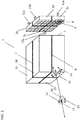
- Figure 1 illustrates a plurality of gamma photon detectors in accordance with certain aspects of the invention.
- a plurality of gamma photon detectors 1 is shown wherein each gamma photon detector comprises a scintillator element 2a, 2b, 2c or 2d in optical communication with a corresponding optical detector pixel array 3a, 3b, 3c, or 3d.
- a scintillator element 2a, 2b, 2c or 2d in optical communication with a corresponding optical detector pixel array 3a, 3b, 3c, or 3d.
- the plurality of gamma photon detectors 1 may for example be disposed around the imaging region of a PET imaging system.
- scintillator elements 2a, 2b, 2c, 2d in Figure 1 are illustrated as being separated from their corresponding optical detector pixel array 3a, 3b, 3c, 3d; however in practice face 5 of exemplary scintillator element 2a and face 6 of its corresponding optical detector pixel array 3a may be in intimate contact, or optically coupled by means of an optically index-matching layer in order to facilitate optical communication between the two.
- the individual scintillator elements exemplified by 2a, 2b, 2c, 2d are optically isolated from one another by means of reflective and light barrier layers 7, 8 in order to prevent the coupling of scintillation light between neighboring scintillator elements.
- Such reflective and light barrier layers 7, 8 may also be used on all surfaces of scintillator elements 2a, 2b, 2c, 2d other than the optical interface with the optical detector pixel array shown in Figure 1 . In this way, scintillation light generated within a scintillator element is retained within that scintillation element until it is detected by its corresponding optical detector pixel array.
- a gamma photon detector exemplified by scintillator element 2a and its corresponding optical detector pixel array 3a shown shaded in Figure 1 , is responsive to the reception of radiation quanta such as gamma photon 10.
- Gamma photon 10 may be one of a pair of oppositely-directed gamma photons 10, 13 formed as a consequence of an annihilation event following radioactive decay, wherein the radioactive decay produces positron 14 and is annihilated by electron 15.
- the source of the radioactive decay may be for example a radiotracer.
- the reception of gamma photon 10 by scintillator element 2a results in the generation of scintillation light 11 which is retained within scintillator element 2a by a combination of total internal reflection and reflective layers 7, 8 until its detection by optical detector pixel array 3a, resulting in electrical signals at array electrical output 12a.
- Optical detector pixel array 3a comprises one or more optical detector pixels 6, shown as dark shaded in Figure 1 , wherein each optical detector pixel 6 comprises one or more pixel cells 9.
- the smallest optical detector element is therefore a pixel cell 9 which may be for example a silicon photomultiplier (SiPM) connected in the Geiger mode.
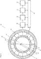
- FIG. 2 illustrates an exemplary PET imaging system in accordance with certain aspects of the invention.
- the exemplary gamma photon detectors of Figure 1 may for example be used in the system illustrated in Figure 2 .
- PET imaging system 20 comprises a plurality of gamma photon detector modules, or more specifically gamma photon detector modules 24, 25 disposed about imaging region 21.
- Each gamma photon detector module 24, 25 may comprise one or more gamma photon detectors such as the gamma photon detector formed by the combination of items 2a and 3a in Figure 1 .
- Each gamma photon detector within gamma photon detector module 24, 25 produces electrical signals indicative of the reception of gamma photons, the electrical signals from which are received by timestamping unit 28 via a bus. Whilst illustrated as a single unit, timestamping unit 28 may be replicated such that one or more timestamping units are associated with each gamma photon detector module 24 thereby providing timestamping functionality locally to the gamma photon detector at which a gamma photon is received. In operation the detection of exemplary gamma photons 22, 23 by gamma photon detector modules 24, 25 respectively results in electrical signals that are received by timestamping unit 28 via bus 26, and bus 27 respectively.
- Each bus 26, 27 represents the one or more array electrical outputs 12a, 12b, 12c, 12d in Figure 1 of the one or more gamma photon detectors within each gamma photon detector module 24, 25.
- timestamping unit 28 issues at least a timestamp indicative of the time of reception of each received gamma photon.
- An integration unit may be further included within timestamping unit 28 to integrate the scintillation light associated with each gamma photon in order to determine its energy. Timestamping unit 28 is in communication with coincidence determination unit 29 which identifies received gamma photons as coincident if their timestamps occur within a narrow time interval of each other, typically +/- 3 ns.
- Coincidence determination unit 29 may further analyze the energy associated with each received gamma photon and reject apparently coincident gamma photons which have a gamma photon energy lying outside a predetermined energy window.
- Coincidence determination unit 29 is in communication with reconstruction processor 30 which constructs a line of response for each pair of received photons deemed coincident and further processes multiple such lines of response in order to reconstruct data representing an image of the originating positions of the coincident gamma photons.
- the reconstruction processor may further take into account the small time difference between received coincident gamma photons in order to better localize their originating position.
- Reconstruction processor 30 is in further communication with image processing unit 31 which is configured to process the data representing the originating positions of the coincident photons into a format suitable for presentation of an image on an output device.
- Image processing unit 31 is in further communication with output device 32 which presents an image, such as a display, a printer and the like.
- Control unit 33 is in communication with all described units of the PET imaging system and coordinates the operations described above.
- a portion of a subject to be imaged such as portion of a human or animal body is positioned in imaging region 21 of the exemplary PET imaging system in Figure 2 .
- the portion may be an organ within a subject in which it is desired to measure the uptake of a radiotracer.
- a radiotracer Prior to the positioning of the portion of the subject in the imaging region 21, a radiotracer may be administered to the subject, and an uptake period may be permitted to lapse.
- a plurality of gamma photon detectors 1 receive gamma photons resulting from radioactive decay events within the imaging region 21, for example from the decay of a radiotracer administered to a subject.
- PET imaging system 20 produces an image indicative of the distribution of the radiotracer within imaging region 21.
- the timing unit and timestamp trigger unit of the present invention find application within timestamping unit 28 in Figure 2 .
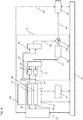
- Figure 3 illustrates a prior art timing scheme used in a Philips Digital Photon Counting (PDPC) PET imaging system.
- PDPC Philips Digital Photon Counting
- scintillator element 40 is in optical communication with optical detector pixel array 41 to form a gamma photon detector.
- a plurality of such gamma photon detectors may be used in the PET imaging system 20 illustrated in Figure 2 .
- scintillation light generated within scintillator element 40 is detected by pixel cells within optical detector pixel array 41.
- Optical detector pixel array 41 comprises one or more optical detector pixels wherein each optical detector pixel comprises one or more pixel cells.
- a pixel cell may be a single optical photon avalanche detector (SPAD), otherwise known as a silicon photomultiplier (SiPM), and may be operated in the Geiger mode. In operation a SiPM, or a pixel cell is initially reset such that its output is in a logical false state. The reception of an optical photon by a SiPM results in the breakdown of its junction and the triggering of a logical true state at its output.
- the smallest optical detector element in optical detector pixel array 41 is therefore a pixel cell wherein each pixel cell can be enabled and disabled individually and its logical output can be read out.
- an optical detector pixel has a pitch of approximately 4 mm and a pixel cell has a pitch of approximately 50 microns.
- An optical detector pixel may therefore comprise thousands of pixel cells, although implementations with one or more pixel cells are also contemplated.
- Pixel cells within optical detector pixel array 41 are arranged in rows, as exemplified by pixel cell rows 42, 43 of which only two are shown for ease of illustration. There may be one or more such pixel cell rows.
- a logical OR operation (not shown) is further performed on the outputs of one or more pixel cells in a pixel cell row 42, 43 and used to generate a row trigger signal at row trigger outputs 48, 49.
- a row trigger output 48, 49 is therefore set into a logical true state when one or more of the pixel cells in its pixel cell row 42, 43 have been triggered into a logical true state.
- scintillator element 40 corresponds to item 2a; optical detector pixel array 41 corresponds to item 3a.
- a timing unit implemented as time to digital converter (TDC) 44, generates a timestamp indicative of the time of reception of a gamma photon by scintillator element 40 when triggered by trigger logic unit 45.
- Validation output 60 of validation logic unit 46 controls the output of the timestamp to control unit 33 such that if the electrical signals at row trigger outputs 48, 49 appear to result from a gamma photon the timestamp is output to control unit 33, and if not, the timestamp is not output and the TDC is reset.
- Optional integrator unit 47 may be used to determine the energy of each received gamma photon by integrating the scintillation light produced in response to its reception.
- the gamma photon energy is a useful parameter in applications such as PET imaging in which a coincidence determination unit may use it to improve the discrimination between scattered and non-scattered gamma photons and thereby determine the validity of a line of response.
- Optional integrator unit 47 may be configured to generate a signal indicative of the total amount of scintillation light detected by the pixel cells within optical detector pixel array 41. The integration by integrator unit 47 may be initiated via control unit 33 when trigger logic unit 45 causes TDC 44 to generate a timestamp.
- Optional control unit 33 may coordinate the various operations described above, may further receive timestamps from TDC 44 and may further control their transfer to coincidence determination unit 29 within PET imaging system 20 illustrated in Figure 1 .
- the reception of a gamma photon by scintillator element 40 in prior art Figure 3 results in the generation of a scintillation light pulse comprising a large number of optical photons.
- the optical photons are detected by pixel cells within optical detector pixel array 41 resulting in a logical true state at row trigger outputs 48, 49 if one or more pixel cells in its corresponding pixel cell row 42, 43 detects an optical photon.
- Scintillation light is characterized by the detection of its optical photons by pixel cells from multiple pixel cell rows 42, 43 and is therefore characterized by a logical true state at multiple row trigger outputs 48, 49.
- Trigger logic unit 45 performs a logical operation on multiple row trigger outputs 48, 49 in order to generate a signal at TDC trigger connection 64 which causes TDC 44 to generate a timestamp when a predetermined logic condition is fulfilled. It is typically desired to generate a timestamp when as few row trigger outputs 48, 49 as possible are in a logical true state in order to optimize the sensitivity of the detection.
- the lowest trigger threshold is therefore achieved by configuring trigger logic unit 45 as an OR logic unit in which TDC trigger connection 64 causes TDC 44 to generate a timestamp when one or more of the row trigger outputs 48, 49 are in a logical true state. Such a configuration corresponds to the generation of a timestamp upon the detection of the first optical photon.
- higher thresholds with improved dark count noise rejection can also be achieved by realizing trigger logic unit 45 with a combination of AND and OR logic having as inputs a predetermined selection of row trigger outputs 48, 49.
- Validation logic unit 46 in prior art Figure 3 includes logic circuitry which receives signals from row trigger outputs 48, 49 indicative of the detection of optical photons in pixel cell rows 42, 43 in order to determine whether these signals originated from a gamma photon.
- Validation logic unit 46 generates a true signal at validation output 60 when a predetermined number of row trigger outputs 48, 49 in optical detector pixel array 41 have been set into a true state indicative of the detection of one or more optical photons by pixel cells in a corresponding pixel cell row 42, 43.
- the threshold number of pixel cells required to change the state of validation output 60 is higher than that required by trigger logic unit 45 to cause TDC 44 to generate a timestamp.
- validation logic unit 46 provides discrimination against noise which typically sets a low total number of pixel cells within optical detector pixel array 41 into a true state, and a scintillation light pulse which sets a much higher total number of pixel cells within optical detector pixel array 41 into a true state. If validation logic unit 46 confirms that the predetermined number of row trigger outputs 48, 49 have been set into a true state, the scintillation light pulse is interpreted as originating from a gamma photon and validation output 60 causes TDC 44 to output the timestamp to control unit 33. The timestamp which was produced when triggered by trigger logic unit 45 is then transferred to control unit 33 from a register (not shown). If validation logic unit 46 does not confirm that the predetermined number of row trigger outputs 48, 49 have been set into a true state then the timestamp is not transferred to control unit 33 and the TDC 44 and integrator unit 47 are reset via control unit 33.
- SiPM optical detectors As stated earlier, a drawback of SiPM optical detectors is the high dark count noise inherent in their Geiger mode operation.
- electrical signals at row trigger outputs 48, 49 caused by dark count noise have similar characteristics to the electrical signals resulting from the detection of a gamma photon, confounding discrimination between the two.
- Dark count noise in pixel cells within pixel cell rows 42, 43 may therefore cause trigger logic unit 45 to cause TDC 44 to generate a timestamp, and correctly fail to set validation output 60 of validation logic unit 46 into a true state and thereby cause TDC 44 to output the timestamp to control unit 33.
- TDC 44 is reset in preparation for generating the next timestamp.
- a timing unit exemplified by a TDC, is caused to generate a timestamp by a timestamp trigger unit based on a pixel cell triggering rate within the optical detector pixel array, thus based on an optical photon detection rate.
- the inventor has found that causing a timing unit to generate a timestamp based on a pixel cell triggering rate provides improved discrimination between the triggering of pixel cells by optical photons and by dark count noise. Consequently the frequency with which dark count noise causes the timing unit to generate a timestamp is reduced, and the proportion of time during which the timing unit is disabled by noise-triggered deadtime is reduced.
- the timing unit is therefore able to timestamp the reception of gamma photons for a greater proportion of the time.
- the improved time utilization of the timing unit advantageously alleviates the cooling requirements of the optical detectors.
- the reduced activity of the timing unit also reduces its own power consumption thereby reducing the temperature of the nearby optical detectors, further reducing their dark count noise.
- the improved timing method furthermore has improved timing accuracy which improves image resolution when used in a PET imaging system.
- timing unit implemented by TDC 44 generates a timestamp when a predetermined number of optical detector pixel cells have been triggered.
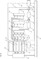
- FIG 4 illustrates an example of a timing unit and timestamp trigger unit 71 in accordance with certain aspects of the invention.
- scintillator element 40 is in optical communication with optical detector pixel array 41 to form a gamma photon detector. Scintillation light generated within scintillator element 40 is detected by optical detector pixel array 41. A plurality of such gamma photon detectors may be used in the PET imaging system 20 illustrated in Figure 2 . Optical photons from for example Cherenkov radiation may be directly detected in the same way although in the absence of scintillator element 40.
- Optical detector pixel array 41 comprises one or more optical detector pixels, each comprising one or more pixel cells.
- a pixel cell may be a single optical photon avalanche detector (SPAD), otherwise known as a silicon photomultiplier (SiPM), and may be operated in the Geiger mode in which the reception of an optical photon results in the breakdown of the junction and a logical true state at the pixel cell output.
- SiPM silicon photomultiplier
- a SiPM or a pixel cell is initially reset such that its output is in a logical false state.
- the reception of an optical photon by a SiPM results in the breakdown of its junction, thereby triggering its output to change to a logical true state.
- the smallest optical detector element in optical detector pixel array 41 is therefore a pixel cell wherein each pixel cell can be enabled and disabled individually and its logical output can be read out.
- an optical detector pixel has a pitch of approximately 4 mm and the pixel cells are arranged in rows with a pitch of approximately 50 microns.
- An optical detector pixel may therefore comprise thousands of pixel cells, although implementations with one or more cells are also contemplated.
- the pixel cells within optical detector pixel array 41 may be arranged in rows, as exemplified by pixel cell rows 42, 43 in Figure 4 of which only two rows are shown for ease of illustration. There may be one or more such pixel cell rows.
- a logical OR operation (not shown) is further performed on the outputs of one or more pixel cells in a pixel cell row 42, 43 and used to generate a row trigger signal at row trigger outputs 48, 49.
- a row trigger output 48, 49 is therefore set into a logical true state when one or more of the pixel cells in its pixel cell row 42, 43 are in a logical true state.
- scintillator element 40 corresponds to item 2a; optical detector pixel array 41 corresponds to item 3a.
- a timing unit exemplified by TDC 44 generates a timestamp indicative of the time of reception of a gamma photon by scintillator element 40 when AND logic 50 generates a logical true state at TDC trigger connection 64.
- An alternative timing unit such as an analogue timing unit may also be used to implement the timing unit.
- Pulse shortening unit 51 comprises one or more monostables 52, 53, each configured to receive electrical signals from a pixel cell row 42, 43 and to generate a logical true output pulse when a signal at its corresponding row trigger output 48, 49 indicates that one or more pixel cells in its corresponding pixel cell row 42, 43 have been triggered into a true state indicative of the detection of an optical photon.
- the period of the monostable pulse may be in the range 0.001 ns to 10 ns, is preferably in the range 0.001 ns to 5 ns, and is even more preferably in the range 0.001 ns to 1 ns, and most preferably in the range 0.001 ns to 0.5 ns.
- a monostable 52, 53 generates a logical true output pulse when a single optical photon has been detected by a pixel cell in its corresponding pixel cell row 42, 43.
- the electrical outputs of monostables 52, 53 in pulse shortening unit 51 are subsequently connected to primary trigger logic unit 54.
- Output 57 of primary trigger logic unit 54 is configured to output a logical true state when a predetermined trigger condition is met.
- primary trigger logic unit 54 performs a logical OR operation such that its output 57 causes delay unit 56 to generate a logical true output pulse at 58 a fixed time, determined by the delay period of delay unit 56, after any one of the monostables in pulse shortening unit 51 meet its threshold condition.
- delay unit 56 is configured to generate a logical true output pulse a fixed time after a single photon is detected in any one of the pixel cells within optical detector pixel array 41.
- primary trigger logic 54 may comprise any combination of logic which causes output 57 to be in a logical true state when the threshold condition for monostables 52, 53 in pulse shortening unit 51 is met for any predetermined selection of pixel cells within optical detector pixel array 41.
- delay unit 56 may be configured to generate a logical true output pulse at output 58 a fixed delay period, determined by the delay period of delay unit 56, after any number, n, of optical photons are detected by pixel cells within optical detector pixel array 41.
- the logical true output pulse is thus created a fixed delay period after the n th optical photon has been detected, or after the n th pixel cell has been triggered. If, within the delay period of delay unit 56, output 59 of secondary trigger logic unit 55 is subsequently set into a true state, output 64 of AND logic 50 causes the TDC to generate a timestamp. Since the time of the timestamp is determined by the time at which the n th optical photon or n th pixel cell was triggered plus the delay period of delay unit 56, the time at which the n th optical photon was detected or the n th pixel cell was triggered can be determined by subtracting the delay period of delay unit 56 from the time of the timestamp. This has useful application in PET imaging in improving the repeatability of timing measurements.
- Secondary trigger logic unit 55 receives electrical signals from one or more row trigger outputs 48, 49. Its output 59 is configured to be in a logical true state when a predetermined logic condition for row trigger outputs 48, 49 is met. This condition may correspond to for example the pixel cell triggering rate exceeding, being less than, being within a predetermined range of, or being equal to a predetermined rate. In this way a timestamp is generated based on a pixel cell triggering rate.
- secondary trigger logic 55 is configured to generate a logical true signal at output 59 when the total number of row trigger outputs 48, 49 in a logical true state exceeds a predetermined number which is greater than that which causes primary trigger logic unit 54 to set its output 54 into a logical true state.
- the number of row trigger outputs 48, 49 required to set secondary trigger logic output 59 into a logical true state may be for example two or more.
- the delay period in delay unit 56 determines the time period during which the pixel cell triggering rate is determined.
- the pixel cell triggering rate is determined by computing the difference between the threshold number of triggered pixel cells required to set secondary trigger logic unit 55 into a true state, and that required to set primary trigger logic unit 54 into a true state, within the delay period of delay unit 56.
- threshold pixel cell triggering rate of one triggered pixel cell per 100 ps, corresponding to one optical photon per 100 ps.
- Pixel cells in pixel cell rows 42, 43 may be reset subsequent to output 57 of primary trigger logic unit 54, or subsequent to output 64 of AND logic 50 in order to prepare the pixels in optical detector pixel array 41 for generating the next timestamp.
- output 58 of delay unit 56 causes TDC 44 to generate a timestamp when the pixel cell triggering rate within optical detector pixel array 41 exceeds a predetermined rate, thus when the optical photon detection rate exceeds a predetermined rate. Furthermore in this configuration the time of the timestamp corresponds to the time at which the first pixel cell was triggered plus the delay period of delay unit 56, permitting subsequent computation of the time of detection of the first triggered pixel cell.
- a timestamp may be generated following the meeting of other pixel cell triggering rate-based conditions.
- Clearly at least one pixel cell must be triggered in order for primary trigger logic unit 54 to sets its output into a high state.
- the generation of a timestamp may furthermore be made conditional to the prior detection of a threshold number of triggered pixel cells by adjusting the condition for primary trigger logic unit 54 to set its output into a logical true state.
- the time of the timestamp is the delay period of delay unit 56 after the meeting of the input condition for primary trigger logic unit 54.
- the circuit in Figure 4 may be configured to generate a timestamp corresponding to the time of detection of the n th optical photon plus the delay period of delay unit 56, wherein the timestamp is conditional upon the initial detection of n triggered optical photons and the subsequent meeting of a pixel cell triggering rate condition.
- Such an implementation advantageously improves the rejection of noise by generating a timestamp based on the profile of detected optical photons.
- the pulse period for monostables in pulse shortening unit 51 in Figure 4 is desirably shorter than the delay period of delay unit 56in order to prevent overlapping trigger pulses at the inputs to primary trigger logic unit 54.
- the delay period of delay unit 56 is made as short as possible in order to rapidly discriminate between dark count noise and electrical signals indicative of the reception of a gamma photon.
- Improved timing performance has been found throughout the following series of ranges for the delay period in delay unit 56: the range 0.001 ns to 200 ns, the range 0.001 ns to 20 ns, the range 0.001 ns to 10 ns, the range 0.001 ns to 1 ns.
- the configuration in Figure 4 may be adapted such that the first optical photon produced by a gamma photon primes AND logic 50, and providing, within the delay period of delay unit 56, that the rate of optical photon generation in scintillator element 40 is subsequently sufficient to cause secondary trigger logic 55 to be in a logical true state, a timestamp is generated by TDC 44.
- the time of detection of the first optical photon may therefore be determined by subtracting the delay period of delay unit 56 from the time of the timestamp.
- the configuration may also be adapted such that the n th optical photon primes AND logic 50 via delay unit 56, and such that k or more optical photons, where k exceeds n, set secondary trigger logic unit 55 into a true logic state.
- a timestamp is generated at a time determined by the delay period after the detection of the n th optical photon, providing the rate condition determined by (k - n) optical photons per period of time determined by the delay period, is exceeded.
- the threshold optical photon detection rate required to generate a timestamp may be adjusted via i) the delay period of delay unit 56 ii) the threshold number of pixel cells that must be set into a logical true state in order to trigger each monostable in pulse shortening unit 51, iii) the threshold number of pixel cells that must be set into a logical true state in order to cause a change in the output of primary trigger logic unit 54, or iv) the threshold number of pixel cells that must be set into a logical true state in order to cause a change in the output of secondary trigger logic unit 55.
- Increasing the threshold optical photon detection rate required to generate a timestamp in general reduces the susceptibility to false triggering of the TDC by dark count noise. Making the threshold rate excessively high reduces the sensitivity to scintillation light pulses resulting from gamma photons since some light pulses will be missed.
- the system in Figure 4 is configured such that the first optical photon primes AND logic 50 via primary trigger logic 54 and the secondary trigger logic 55 is configured to cause AND logic 50 to cause TDC 44 to generate a timestamp at a higher trigger level, thus when a higher number of optical photons have been subsequently detected within the delay period of delay unit 56.
- a typical scintillator element material, LYSO produces approximately 2000 photons in response to the reception of a single gamma photon at 511 keV. These are subject to a decay time of approximately 40 ns in LYSO and lead to an initial optical photon flux of 50 photons/ ns.
- Significant noise discrimination can be provided by setting delay unit 56 to have a delay period of 1 ns in which case output 59 of secondary trigger logic 55 should be configured to be in a logical true state when the detected photon flux exceeds approximately 5 photons/ ns.
- Optional validation logic unit 46 in Figure 4 includes logic circuitry which receives signals from row trigger outputs 48, 49 indicative of the detection of optical photons in pixel cell rows 42, 43 in order to determine whether these signals originated from a gamma photon.
- Optional validation logic unit 46 may thus be configured to generate a true signal at validation output 60 when a predetermined number of row trigger outputs 48, 49 in optical detector pixel array 41 have been set into a true state indicative of the detection of one or more optical photons by pixel cells in a corresponding pixel cell row 42, 43.
- the threshold number of pixel cells required to change the state of validation output 60 is preferably set to a higher number than that required by trigger logic unit 45 to cause TDC 44 to generate a timestamp.
- validation logic unit 46 can be used to provide additional discrimination against noise which typically sets a low total number of pixel cells within optical detector pixel array 41 into a true state, and a scintillation light pulse resulting from the reception of a gamma photon by scintillator element 40 which sets a much higher total number of pixel cells within optical detector pixel array 41 into a true state. If optional validation logic unit 46 confirms that the predetermined number of row trigger outputs 48, 49 have been set into a true state, the scintillation light pulse is interpreted as originating from a gamma photon and validation output 60 causes TDC 44 to output the timestamp to control unit 33.
- the timestamp which was produced when triggered by trigger logic unit 45 is then transferred to control unit 33 from a register (not shown). If optional validation logic unit 46 does not confirm that the predetermined number of row trigger outputs 48, 49 have been set into a true state then the timestamp is not transferred to control unit 33 and the TDC 44 and integrator unit 47 are reset via control unit 33.
- the predetermined number of row trigger outputs 48, 49 required to set the output of optional validation logic unit 46 into the valid state are such that a true validation output 60 is generated in response to a scintillation light pulse within approximately 10 ns of a logical true signal at trigger connection 64. In this way, if noise causes TDC 44 to generate a timestamp its reset may be initiated within 10 ns and therefore without too long a delay.
- Optional integrator unit 47 in Figure 4 may be used to determine the energy of each received gamma photon by integrating the scintillation light produced in response to its reception.
- the energy of each gamma photon is a parameter that may be used in high energy physics applications such as PET imaging in which it can be used by a coincidence determination unit to improve the discrimination between scattered and non-scattered gamma photons and thereby determine the validity of a line of response from timewise coincident gamma photons.
- Integrator unit 47 may thus be configured to generate a signal indicative of the total amount of scintillation light detected by the pixel cells within optical detector pixel array 41.
- the integration may be performed by intermittently transferring the logical output of pixel cells in pixel cell rows 42, 43 to integrator unit 47 in a multiplexed fashion and summing the number of pixel cells in a logical true state.
- the integration by integrator unit 47 may be initiated via control unit 33 when trigger logic unit 45 causes TDC 44 to generate a timestamp.
- Optional control unit 33 in Figure 4 may coordinate the various operations described above, and may further receive timestamps from TDC 44, and further to control their transfer to coincidence determination unit 29 within PET imaging system 20 illustrated in Figure 1 .
- Figure 5 illustrates an embodiment of a timing unit and timestamp trigger unit in accordance with certain aspects of the invention.
- the embodiment in Figure 5 is configured to generate a timestamp following the meeting of both a first pixel cell triggering rate condition and the subsequent meeting of a second pixel cell triggering rate condition.
- Improved noise rejection is provided by the requirement that the triggering rate conditions are met at subsequent points in time before the timestamp is generated. This allows for the generation of a timestamp based on the profile of the scintillation light's optical photon detection rate.
- the timing unit, implemented by exemplary TDC 44 is not started until there is an even higher probability that the electrical signals from pixel cells within the optical detector pixel array result from scintillation light.
- timing unit implemented by exemplary TDC 44 may alternatively be implemented by another timing unit such as an analogue timing unit.
- Figure 5 includes tertiary trigger logic unit 63 which receives electrical signals from one or more row trigger outputs 48, 49, 67, 68. Its output 69 is configured to be in a logical true state when the number of pixel cells triggered within a delay period determined by delay unit 61 meets a predetermined count condition; thus the pixel cell triggering rate meets a predetermined rate condition as earlier described with reference to Figure 4 . Output 69 of tertiary trigger logic unit 63 in Figure 5 may be configured to be in a logical true state when any number of optical photons are detected by pixel cells within optical detector pixel array 41.
- this output may be configured to be in a logical true state when this number is equaled, exceeded, not exceeded or is within a predetermined range.
- a timestamp may be issued by TDC 44 dependent upon whether the pixel cell triggering rate determined by tertiary trigger logic 63 in combination with delay unit 2 is greater than, less than, equal to, or is within a predetermined range of a predetermined rate.
- Second delay unit 61 in Figure 5 operates in the same manner as delay unit 56 in Figure 4 .
- Pixel cells in pixel cell rows 42, 43, 65, 66 may be reset subsequent to output 57 of primary trigger logic unit 54, or subsequent to output 64 of AND logic 62 in order to prepare the pixels in optical detector pixel array 41 for generating the next timestamp.
- Additional AND logic 62 is also included in the embodiment in Figure 5 . Whilst additional pixel cell rows 65, 66 and their corresponding outputs are also illustrated in Figure 5 in order to illustrate the possibility of scaling the circuit to larger numbers of optical detector pixels it is to be appreciated that the circuit may be adapted to operate with one or more such pixel cell rows wherein each row includes one or more pixel cells.
- the embodiment in Figure 5 may be configured to take advantage of the observation that a scintillation light pulse generated in a scintillator element 40 following the reception of a gamma photon is typically characterized by a rapid initial optical photon detection rate followed by a reduction in the optical photon detection rate.
- a scintillation light pulse generated in a scintillator element 40 following the reception of a gamma photon is typically characterized by a rapid initial optical photon detection rate followed by a reduction in the optical photon detection rate.
- Such a profile is typical of a scintillation light pulse from a gamma photon in a PET imaging system in which a rapid initial increase in scintillation light is followed by an exponential decay.
- the decay constant may be in the order of 40 ns.
- the profile from dark count noise, which is randomly generated results in a more uniform pixel cell triggering rate.
- Optical photons from for example Cherenkov radiation may be directly detected in the same way as described above although in the absence of scintillator element 40.
- These characteristic differences in the pixel cell triggering rate may be exploited in the second embodiment illustrated in Figure 5 by making the threshold pixel cell triggering rate required to set output 70 of secondary trigger logic 55 dependent upon a particular rate being exceeded, and the threshold pixel cell triggering rate required to set output 69 of tertiary trigger logic 63 dependent upon a particular rate being exceeded, not exceeded or within a narrow range.
- the generation of a timestamp can be made dependent upon any desired profile of pixel cell triggering rate, thus optical photon generation rate, determined at two points in time.
- the monostables in pulse shortener unit 51 each have a period of 0.5 ns
- delay unit 56 has a delay period of 1 ns
- delay unit 61 has a delay period of 10 ns.
- output 57 of primary trigger logic 54 is configured to be in a logical true state when any one of its inputs from pulse shortener unit 51 are in a logical true state.
- Output 59 of secondary trigger logic unit 55 is configured to be in a logical true state when the number of triggered cells in optical detector pixel array 41 during the 1 ns delay period of delay unit 56, thus the pixel cell triggering rate, corresponds to a gamma photon reception rate exceeding 10 6 counts per second.
- Output 69 of tertiary trigger logic unit 63 is configured to be in a logical true state when the number of triggered cells in optical detector pixel array 41 during the 10 ns period of delay unit 61, thus the pixel cell triggering rate, corresponds to a gamma photon reception rate exceeding 10 5 counts per second.
- Pulse shortener unit 1 receives signals from row trigger outputs 48, 49, 67, 68 which correspond to all pixel cell rows 42, 43, 65, 66 in optical detector pixel array 41. In this way when any one of the pixel cells within optical detector pixel array 41 is set into a logical true state the output of primary trigger logic 54 is set into a logical true state for a period of 0.5 ns.
- Delay unit 56 delays the propagation of this pulse to AND logic 50 for a delay period of 1 ns.
- secondary trigger logic unit 55 determines whether the row trigger outputs 48, 49, 67, 68 at its input meet its predetermined rate condition corresponding to a gamma photon reception rate exceeding 10 6 counts per second. If this condition is met within the 1 ns delay period of delay unit 56 then its output 70 is set into a logical true state, which at the end of the 1 ns delay period of delay unit 56 causes a logical true output from AND logic 50.
- Delay unit 61 delays the propagation of this pulse to AND logic 62 for a delay period of 10 ns.
- tertiary trigger logic unit 63 determines whether within this second 10 ns delay period the row trigger outputs 48, 49, 67, 68 at its input meet its predetermined rate condition corresponding to a gamma photon reception rate exceeding 10 5 counts per second. If this condition is met within the 10 ns period of delay unit 61 then its output 69 is set into a logical true state, which at the end of the 10 ns period of delay unit 61 causes a logical true output at TDC trigger connection 64, the output from AND logic 62 thereby causing TDC 44 to generate a timestamp.
- the pixel cells in optical detector pixel array may be reset subsequent to either of outputs 57, 70 or 69 or 64 becoming set into the true logic state in order to prepare the pixel cells for generating the next timestamp.
- the configuration may further be reconfigured for example between or during the use of the circuit in the execution of a PET imaging scan. In so doing the system can be reconfigured to adjust both sensitivity and noise rejection during use.
- optional integrator unit 47 illustrated in Figure 5 may further integrate the scintillation light from a received gamma photon.
- optional validation logic unit 46 may provide further discrimination against noise by controlling the output of the timestamp to control unit 33 from TDC 44, or its rejection, based on a total number of triggered pixel cells within optical detector pixel array 41.
- Optional control unit 33 may further coordinate the various described processes.
- the example illustrated in Figure 4 is further supplied with second TDC similar in operation to TDC 44 and referred-to hereinafter as a reference time-to-digital converter (RTDC).
- the RTDC is configured to receive electrical signals from output 57 of primary trigger logic unit 54 and to generate a second timestamp when this output makes a transition from a logical false state to a logical true state. In this way a timestamp is not only generated when the triggering rate condition for the secondary trigger logic unit is met, but a second timestamp is also generated when the condition for primary trigger logic unit 54 is met.
- the second timestamp relating to the condition for primary trigger logic unit 54 is indicative of the time of detection of a particular number of optical photons, rather than indicative of a particular optical photon detection rate condition.
- a timestamp generated by the RTDC can be used to provide information relating to the shape of the scintillation light pulse that triggered primary trigger logic 54. This pulse shape information can be subsequently used to perform a time walk correction or to estimate the depth of interaction of a gamma photon in scintillator element 40 and thereby improve the spatial resolution of detection of the original gamma photon.
- This depth of interaction can subsequently be used in a PET imaging system to further improve the spatial resolution of determining coincident pairs of gamma photons as it allows for discrimination based on the angle of incidence of a gamma photon.
- This information can be compared for two apparently coincident gamma photons in order to reject gamma photons that appear coincident but which, due to their incidence angles, are actually the subject of a parallax error.
- the trigger logic units 54 and 55 may be made programmable in order that the sampling of characteristics of the scintillation light pulse from a number of points in time is possible.
- the circuit described in this third embodiment may also be adapted by including additional trigger logic units, each with a corresponding time to digital converter in order to either generate additional timestamps at different times throughout the scintillation light pulse, or as a precondition for TDC 44 generating a timestamp. Additional timestamps can be used to improve the determination of the shape of the scintillation light pulse and thereby provide an even more accurate time walk correction, reduce timing jitter, or improved an estimate of the depth of interaction. When used as a precondition for TDC 44 to generate a timestamp the resulting timestamp has the benefit of being generated with an even higher probability of the electrical signals from the pixel cells originating from a gamma photon.
- the system in Figure 4 is configured such that the first detected optical photon causes output 57 of primary trigger logic 54 to be in a logical true state, and such that secondary trigger logic 55 causes AND logic 50 to cause TDC 44 to generate a timestamp when the pixel cell triggering rate for pixel cells within optical detector pixel array 41 exceeds the expected initial rate from a gamma photon. This rate could be for example 50 optical photons/ ns.
- Delay unit 56 may be configured to have a delay period of for example 1 ns.
- the RTDC, receiving electrical signals from output 57 of primary trigger logic unit 54 is therefore configured to generate a timestamp when the first optical photon is detected.
- a timewalk correction can be performed by multiplying the clock period of the TDC by a scaling factor in order that this is the case.
- a depth of interaction calculation for a radiation quant in the scintillator element may be performed in order to improve the spatial resolution of a PET imaging system.
- a depth of interaction calculation may be performed by a depth-of-interaction calculation unit configured to compute a depth of interaction using a lookup table or a statistical function relating time differences to a depth of interaction in the scintillator element. Such a lookup table or statistical function may be generated from heuristic or simulated time difference information based on the geometry of the scintillator element.
- the embodiment illustrated in Figure 5 is further supplied with second TDC referred-to hereinafter as a reference time-to-digital converter (RTDC), and a third TDC; both additional TDCs being similar in operation to TDC 44.
- the second TDC, or RTDC is configured to receive electrical signals from output 57 of primary trigger logic unit 54 and to generate a second timestamp when a signal at this output makes a transition from a logical false state to a logical true state.
- the third TDC is configured to receive electrical signals from output 70 of secondary trigger logic unit 55 and to generate a third timestamp when this output makes a transition from a logical false state to a logical true state.
- a first timestamp is generated by TDC 44 when the triggering conditions for the primary, secondary and tertiary trigger logic units 54, 55, and 63 respectively have been met. In practice this is the last of the three timestamps to be generated.
- a second timestamp is generated when the condition for primary trigger logic unit 54 is met. The second timestamp is indicative of the detection of a particular number of optical photons.
- the third timestamp relates to the condition for secondary trigger logic unit 55 and is indicative that a predetermined pixel cell triggering rate for pixel cells within optical detector pixel array 41 has been met.
- the additional second and third timestamps provide further information relating to the shape of the scintillation light pulse that triggered primary trigger logic 54. As with the third embodiment this pulse shape information may subsequently be used to perform a time walk correction or to estimate the depth of interaction of the gamma photon in scintillator element 40 and thereby improve the spatial resolution of detection of the original gamma photon.
- the circuit described in this fourth embodiment may also be extended by adding one or more further trigger logic units, each with a corresponding time to digital converter in order to generate additional timestamps at different times throughout the scintillation light pulse. Such timestamps can likewise be used to improve the determination of the shape of a scintillation light pulse and thereby provide an even more accurate time walk correction or an improved estimate of the depth of interaction.
- the circuit in Figure 5 is configured such that the monostables in pulse shortener unit 51 each have a period of 0.5 ns, delay unit 56 has a delay period of 1 ns and delay unit 61 has a delay period of 10 ns. Furthermore output 57 of primary trigger logic 54 is configured to be in a logical true state when any one of its inputs from pulse shortener unit 51 are in a logical true state. Output 70 of secondary trigger logic unit 55 is configured to be in a logical true state when the number of pixel cells triggered in optical detector pixel array 41 during the 1 ns period of delay unit 56 corresponds to a gamma photon reception rate exceeding 10 6 counts per second.
- Output 69 of tertiary trigger logic unit 63 is configured to be in a logical true state when the number of triggered cells in optical detector pixel array 41 during the 10 ns period of delay unit 61 corresponds to a gamma photon reception rate exceeding 10 5 counts per second.
- Pulse shortener unit 1 receives signals from row trigger outputs 48, 49, 67, 68 which correspond to all pixel cell rows 42, 43, 65, 66 in optical detector pixel array 41. In this way when any one of the pixel cells within optical detector pixel array 41 is set into a logical true state the output of primary trigger logic 54 is set into a logical true state for a period of 0.5 ns.
- the reference TDC (not shown) connected to output 57 thus generates a timestamp when this condition is met.
- the output of secondary trigger logic unit 55 is configured to be in the logical true state when the pixel cell triggering rate for pixel cells within optical detector pixel array 41 corresponds to a gamma photon reception rate exceeding 10 6 counts per second.
- a third TDC thus generates a timestamp when this condition is met.
- TDC 44 generates a timestamp.
- a timing unit and a timestamp trigger unit for timestamping detected radiation quanta with improved noise rejection has been described with particular reference to a PET imaging system.
- the invention has further application in the detection of radiation quanta in high energy particle physics applications as well as in the direct detection of radiation quanta in the form of optical photons such as Cherenkov radiation.
- Improved noise rejection is achieved by the cooperation in which the timestamp trigger unit causes the timing unit to generate a timestamp based on a first and second pixel cell triggering rates for pixel cells within an optical detector pixel array.
- Improved timing resolution is achieved by the disclosed invention whose improved noise rejection permits the generation of a timestamp following the detection of fewer optical photons.
- the cooling requirements of the optical detectors are also alleviated owing to the improved noise rejection and the reduction in the false triggering rate, enabling their operation at closer to room temperature.
Landscapes
- Physics & Mathematics (AREA)
- Health & Medical Sciences (AREA)
- Life Sciences & Earth Sciences (AREA)
- General Physics & Mathematics (AREA)
- High Energy & Nuclear Physics (AREA)
- Molecular Biology (AREA)
- Spectroscopy & Molecular Physics (AREA)
- Nuclear Medicine (AREA)
- Measurement Of Radiation (AREA)
Priority Applications (1)
| Application Number | Priority Date | Filing Date | Title |
|---|---|---|---|
| EP14709220.9A EP2965120B1 (en) | 2013-03-08 | 2014-02-28 | Timestamping detected radiation quanta |
Applications Claiming Priority (3)
| Application Number | Priority Date | Filing Date | Title |
|---|---|---|---|
| EP13158382 | 2013-03-08 | ||
| PCT/EP2014/053990 WO2014135465A1 (en) | 2013-03-08 | 2014-02-28 | Timestamping detected radiation quanta |
| EP14709220.9A EP2965120B1 (en) | 2013-03-08 | 2014-02-28 | Timestamping detected radiation quanta |
Publications (2)
| Publication Number | Publication Date |
|---|---|
| EP2965120A1 EP2965120A1 (en) | 2016-01-13 |
| EP2965120B1 true EP2965120B1 (en) | 2017-12-20 |
Family
ID=47843139
Family Applications (1)
| Application Number | Title | Priority Date | Filing Date |
|---|---|---|---|
| EP14709220.9A Active EP2965120B1 (en) | 2013-03-08 | 2014-02-28 | Timestamping detected radiation quanta |
Country Status (6)
| Country | Link |
|---|---|
| US (1) | US10078141B2 (enExample) |
| EP (1) | EP2965120B1 (enExample) |
| JP (1) | JP6306062B2 (enExample) |
| CN (1) | CN105008962B (enExample) |
| RU (1) | RU2642172C2 (enExample) |
| WO (1) | WO2014135465A1 (enExample) |
Cited By (1)
| Publication number | Priority date | Publication date | Assignee | Title |
|---|---|---|---|---|
| TWI863966B (zh) * | 2019-02-20 | 2024-12-01 | 南韓商三星電子股份有限公司 | 確定光脈衝在光脈衝源與光感測器陣列的畫素之間的行進時間的系統及方法 |
Families Citing this family (31)
| Publication number | Priority date | Publication date | Assignee | Title |
|---|---|---|---|---|
| CN106716179B (zh) * | 2014-09-23 | 2019-08-20 | 皇家飞利浦有限公司 | 数字正电子发射断层摄影中的飞行时间校准 |
| WO2016067431A1 (ja) * | 2014-10-30 | 2016-05-06 | 株式会社島津製作所 | 放射線検出器 |
| FR3032081B1 (fr) * | 2015-01-28 | 2018-02-16 | Weeroc | Circuit electronique configure pour controler un module d'acquisition d'un dispositif de detection de photons, module d'acquisition, procede de controle, et programme d'ordinateur correspondant. |
| CA2882972A1 (en) * | 2015-02-24 | 2016-08-24 | Gaston Beaulieu | Vertically integrated industrial scale multilevel closed ecosystem greenhouse |
| US9606245B1 (en) | 2015-03-24 | 2017-03-28 | The Research Foundation For The State University Of New York | Autonomous gamma, X-ray, and particle detector |
| CN106388768A (zh) * | 2015-11-19 | 2017-02-15 | 南京瑞派宁信息科技有限公司 | 一种切伦科夫辐射成像方法与系统 |
| US9986621B2 (en) | 2016-01-22 | 2018-05-29 | Lumigrow, Inc. | Lighting system for growing plants which provides a location indication |
| US10261201B2 (en) | 2016-04-04 | 2019-04-16 | General Electric Company | Method for improving timing resolution using depth of interaction correction in PET detector |
| US9817134B1 (en) * | 2016-09-12 | 2017-11-14 | General Electric Company | Universal readout for light-sharing detector |
| CN107942369A (zh) * | 2016-10-13 | 2018-04-20 | 中国辐射防护研究院 | 一种基于脉冲时间甄别的硅光电倍增器降噪方法与系统 |
| CN106443747B (zh) * | 2016-11-15 | 2020-05-29 | 中派科技(深圳)有限责任公司 | 用于测量高能光子到达时间的方法及装置 |
| NL2018060B1 (en) * | 2016-12-23 | 2018-07-02 | Univ Delft Tech | Bismuth silicate as detector material for tof-pet |
| CN111149350B (zh) * | 2017-09-28 | 2022-02-22 | 苹果公司 | 使用事件相机生成静态图像 |
| JP7132796B2 (ja) * | 2018-08-30 | 2022-09-07 | 浜松ホトニクス株式会社 | チェレンコフ検出器、チェレンコフ検出器設定方法およびpet装置 |
| DE102019204388A1 (de) * | 2019-03-28 | 2020-10-01 | Siemens Healthcare Gmbh | Röntgendetektor, medizinische Untersuchungseinrichtung und Verfahren zum Betrieb eines Röntgendetektors |
| CN110507344B (zh) * | 2019-09-04 | 2022-05-13 | 上海联影医疗科技股份有限公司 | 一种符合判选方法、装置、设备及存储介质 |
| EP4513153A3 (en) | 2019-07-19 | 2025-05-28 | Avago Technologies International Sales Pte. Limited | Recharge circuit for digital silicon photomultipliers |
| EP4000177A1 (en) | 2019-07-19 | 2022-05-25 | Koninklijke Philips N.V. | Time-domain filtering of gamma events |
| US11271747B2 (en) * | 2019-09-16 | 2022-03-08 | Lawrence Livermore National Security, Llc | Optical authentication of images |
| JP2021092437A (ja) * | 2019-12-10 | 2021-06-17 | ソニーセミコンダクタソリューションズ株式会社 | 受光装置および受光回路 |
| CN110988960B (zh) * | 2019-12-11 | 2024-10-22 | 湖北锐世数字医学影像科技有限公司 | 探测装置和pet成像系统 |
| EP3859400B1 (en) * | 2020-01-31 | 2025-11-05 | Canon Medical Systems Corporation | Radiation imaging device and radiation imaging method |
| CN111707385B (zh) * | 2020-06-19 | 2021-05-07 | 上海交通大学 | 基于时间飞行探测技术实现时间戳玻色采样量子计算系统 |
| GB2616905A (en) * | 2022-03-25 | 2023-09-27 | British Telecomm | Quantum timestamping |
| EP4254017A1 (en) | 2022-03-28 | 2023-10-04 | Koninklijke Philips N.V. | Photon counting detector and photon counting method |
| EP4273587A1 (en) | 2022-05-04 | 2023-11-08 | Koninklijke Philips N.V. | Photon counting detector and photon counting method |
| EP4276496A1 (en) | 2022-05-10 | 2023-11-15 | Koninklijke Philips N.V. | Photon counting detector and photon counting method |
| WO2024178501A1 (en) * | 2023-02-27 | 2024-09-06 | The Governing Council Of The University Of Toronto | Method and system for single-photon imaging |
| US12449554B2 (en) * | 2023-10-05 | 2025-10-21 | Cintilight, Llc | Scintillator detectors and methods for positron emission tomography |
| CN118041444B (zh) * | 2024-04-08 | 2024-06-14 | 中国科学院空间应用工程与技术中心 | 一种用于计算光脉冲信号传输时间延迟的方法 |
| CN118282506B (zh) * | 2024-04-08 | 2024-11-08 | 中国科学院空间应用工程与技术中心 | 一种用于光电探测阵列的时间延迟校准方法和通信装置 |
Family Cites Families (11)
| Publication number | Priority date | Publication date | Assignee | Title |
|---|---|---|---|---|
| KR101273965B1 (ko) * | 2005-04-22 | 2013-06-12 | 코닌클리케 필립스 일렉트로닉스 엔.브이. | 검출기 픽셀, 방사선 검출기, tof-pet 영상화 시스템, 신틸레이터와 함께 수행되는 방법, 및 의료 영상을 생성하는 방법 |
| US7610175B2 (en) * | 2006-02-06 | 2009-10-27 | Agilent Technologies, Inc. | Timestamping signal monitor device |
| CN101600972B (zh) | 2006-07-28 | 2012-08-29 | 皇家飞利浦电子股份有限公司 | 正电子发射断层摄影中的飞行时间测量 |
| CN101680953B (zh) * | 2007-05-16 | 2014-08-13 | 皇家飞利浦电子股份有限公司 | 虚拟pet探测器和用于pet的准像素化读出方案 |
| JP5701616B2 (ja) * | 2008-03-13 | 2015-04-15 | コーニンクレッカ フィリップス エヌ ヴェ | 画像診断装置、画像診断方法及び信号処理回路の電力消費を減少させる方法 |
| JP5024566B2 (ja) | 2009-03-18 | 2012-09-12 | 株式会社島津製作所 | Pet装置の同時計数のタイミング補正値を求める方法 |
| US8492705B2 (en) * | 2009-10-23 | 2013-07-23 | Saint-Gobain Ceramics & Plastics, Inc. | Radiation detector and method of using a radiation detector |
| US9091771B2 (en) * | 2011-07-07 | 2015-07-28 | Siemens Aktiengesellschaft | System and method for improving detection of gamma interactions in a positron emission tomography system |
| US8933409B2 (en) | 2011-07-20 | 2015-01-13 | Siemens Medical Solutions Usa, Inc. | Depth-of-interaction in an imaging device |
| US8779367B2 (en) | 2012-02-20 | 2014-07-15 | General Electric Company | System and method for correcting timing errors in a medical imaging system |
| US8969814B2 (en) | 2012-08-20 | 2015-03-03 | Siemens Medical Solutions Usa, Inc. | System and method of determining timing triggers for detecting gamma events for nuclear imaging |
-
2014
- 2014-02-28 JP JP2015560635A patent/JP6306062B2/ja active Active
- 2014-02-28 RU RU2015142655A patent/RU2642172C2/ru active
- 2014-02-28 EP EP14709220.9A patent/EP2965120B1/en active Active
- 2014-02-28 WO PCT/EP2014/053990 patent/WO2014135465A1/en not_active Ceased
- 2014-02-28 US US14/772,177 patent/US10078141B2/en active Active
- 2014-02-28 CN CN201480012562.6A patent/CN105008962B/zh active Active
Cited By (1)
| Publication number | Priority date | Publication date | Assignee | Title |
|---|---|---|---|---|
| TWI863966B (zh) * | 2019-02-20 | 2024-12-01 | 南韓商三星電子股份有限公司 | 確定光脈衝在光脈衝源與光感測器陣列的畫素之間的行進時間的系統及方法 |
Also Published As
| Publication number | Publication date |
|---|---|
| WO2014135465A1 (en) | 2014-09-12 |
| US10078141B2 (en) | 2018-09-18 |
| CN105008962B (zh) | 2019-01-18 |
| CN105008962A (zh) | 2015-10-28 |
| JP2016513788A (ja) | 2016-05-16 |
| EP2965120A1 (en) | 2016-01-13 |
| JP6306062B2 (ja) | 2018-04-04 |
| RU2015142655A (ru) | 2017-04-13 |
| RU2642172C2 (ru) | 2018-01-24 |
| US20160011321A1 (en) | 2016-01-14 |
Similar Documents
| Publication | Publication Date | Title |
|---|---|---|
| EP2965120B1 (en) | Timestamping detected radiation quanta | |
| US9677931B2 (en) | Detection of radiation quanta using an optical detector pixel array and pixel cell trigger state sensing circuits | |
| US7129495B2 (en) | Method and apparatus for timing calibration in a PET scanner | |
| KR101690318B1 (ko) | 디지털 실리콘 광전자증배기들의 시간 분해능을 개선하기 위한 방법 | |
| EP2820450B1 (en) | Method and system for synchronizing positron emission tomography (pet) detector modules | |
| US8610081B2 (en) | Systems and methods for generating control signals in radiation detector systems | |
| US8969814B2 (en) | System and method of determining timing triggers for detecting gamma events for nuclear imaging | |
| US8822933B2 (en) | Time-to-digital converter for a medical imaging system | |
| US9151851B2 (en) | Mulitplexing device for a medical imaging system | |
| US9091771B2 (en) | System and method for improving detection of gamma interactions in a positron emission tomography system | |
| CN112587159B (zh) | 用于pet检测器的方法和系统 | |
| US20130256536A1 (en) | Methods and systems for determining timing recovery information in a positron emission tomography (pet) system | |
| Schug et al. | First evaluations of the neighbor logic of the digital SiPM tile | |
| US10007011B2 (en) | System for acquisition of tomographic measurement data | |
| KR101352771B1 (ko) | 시프트 레지스터를 이용한 동시계수회로 및 이를 포함하는 pet 데이터 획득 시스템, 방사선 계수시스템 및 의료진단기기 | |
| CN113835113B (zh) | 一种pet中的模块间散射数据收集方法 | |
| WO2006080004A2 (en) | Method and system for x-ray radiation imaging | |
| CN112022189A (zh) | 图像重建方法、装置、设备及pet系统 | |
| CN119138912A (zh) | 用于飞行时间正电子发射断层摄影的系统和方法 | |
| US9778383B2 (en) | Transmission of PET-signals by means of time division multiplexing | |
| Gasparini et al. | Characterizing single-and multiple-timestamp time of arrival estimators with digital SiPM PET detectors | |
| JPH11352232A (ja) | ポジトロンイメージング装置 |
Legal Events
| Date | Code | Title | Description |
|---|---|---|---|
| PUAI | Public reference made under article 153(3) epc to a published international application that has entered the european phase |
Free format text: ORIGINAL CODE: 0009012 |
|
| 17P | Request for examination filed |
Effective date: 20151008 |
|
| AK | Designated contracting states |
Kind code of ref document: A1 Designated state(s): AL AT BE BG CH CY CZ DE DK EE ES FI FR GB GR HR HU IE IS IT LI LT LU LV MC MK MT NL NO PL PT RO RS SE SI SK SM TR |
|
| AX | Request for extension of the european patent |
Extension state: BA ME |
|
| DAX | Request for extension of the european patent (deleted) | ||
| 17Q | First examination report despatched |
Effective date: 20170323 |
|
| GRAP | Despatch of communication of intention to grant a patent |
Free format text: ORIGINAL CODE: EPIDOSNIGR1 |
|
| INTG | Intention to grant announced |
Effective date: 20170621 |
|
| GRAS | Grant fee paid |
Free format text: ORIGINAL CODE: EPIDOSNIGR3 |
|
| GRAA | (expected) grant |
Free format text: ORIGINAL CODE: 0009210 |
|
| AK | Designated contracting states |
Kind code of ref document: B1 Designated state(s): AL AT BE BG CH CY CZ DE DK EE ES FI FR GB GR HR HU IE IS IT LI LT LU LV MC MK MT NL NO PL PT RO RS SE SI SK SM TR |
|
| REG | Reference to a national code |
Ref country code: GB Ref legal event code: FG4D |
|
| REG | Reference to a national code |
Ref country code: CH Ref legal event code: EP |
|
| REG | Reference to a national code |
Ref country code: IE Ref legal event code: FG4D |
|
| REG | Reference to a national code |
Ref country code: AT Ref legal event code: REF Ref document number: 956857 Country of ref document: AT Kind code of ref document: T Effective date: 20180115 |
|
| REG | Reference to a national code |
Ref country code: DE Ref legal event code: R096 Ref document number: 602014018718 Country of ref document: DE |
|
| REG | Reference to a national code |
Ref country code: FR Ref legal event code: PLFP Year of fee payment: 5 |
|
| REG | Reference to a national code |
Ref country code: NL Ref legal event code: MP Effective date: 20171220 |
|
| PG25 | Lapsed in a contracting state [announced via postgrant information from national office to epo] |
Ref country code: LT Free format text: LAPSE BECAUSE OF FAILURE TO SUBMIT A TRANSLATION OF THE DESCRIPTION OR TO PAY THE FEE WITHIN THE PRESCRIBED TIME-LIMIT Effective date: 20171220 Ref country code: SE Free format text: LAPSE BECAUSE OF FAILURE TO SUBMIT A TRANSLATION OF THE DESCRIPTION OR TO PAY THE FEE WITHIN THE PRESCRIBED TIME-LIMIT Effective date: 20171220 Ref country code: FI Free format text: LAPSE BECAUSE OF FAILURE TO SUBMIT A TRANSLATION OF THE DESCRIPTION OR TO PAY THE FEE WITHIN THE PRESCRIBED TIME-LIMIT Effective date: 20171220 Ref country code: NO Free format text: LAPSE BECAUSE OF FAILURE TO SUBMIT A TRANSLATION OF THE DESCRIPTION OR TO PAY THE FEE WITHIN THE PRESCRIBED TIME-LIMIT Effective date: 20180320 |
|
| REG | Reference to a national code |
Ref country code: LT Ref legal event code: MG4D |
|
| REG | Reference to a national code |
Ref country code: AT Ref legal event code: MK05 Ref document number: 956857 Country of ref document: AT Kind code of ref document: T Effective date: 20171220 |
|
| PG25 | Lapsed in a contracting state [announced via postgrant information from national office to epo] |
Ref country code: LV Free format text: LAPSE BECAUSE OF FAILURE TO SUBMIT A TRANSLATION OF THE DESCRIPTION OR TO PAY THE FEE WITHIN THE PRESCRIBED TIME-LIMIT Effective date: 20171220 Ref country code: RS Free format text: LAPSE BECAUSE OF FAILURE TO SUBMIT A TRANSLATION OF THE DESCRIPTION OR TO PAY THE FEE WITHIN THE PRESCRIBED TIME-LIMIT Effective date: 20171220 Ref country code: HR Free format text: LAPSE BECAUSE OF FAILURE TO SUBMIT A TRANSLATION OF THE DESCRIPTION OR TO PAY THE FEE WITHIN THE PRESCRIBED TIME-LIMIT Effective date: 20171220 Ref country code: BG Free format text: LAPSE BECAUSE OF FAILURE TO SUBMIT A TRANSLATION OF THE DESCRIPTION OR TO PAY THE FEE WITHIN THE PRESCRIBED TIME-LIMIT Effective date: 20180320 Ref country code: GR Free format text: LAPSE BECAUSE OF FAILURE TO SUBMIT A TRANSLATION OF THE DESCRIPTION OR TO PAY THE FEE WITHIN THE PRESCRIBED TIME-LIMIT Effective date: 20180321 |
|
| PG25 | Lapsed in a contracting state [announced via postgrant information from national office to epo] |
Ref country code: NL Free format text: LAPSE BECAUSE OF FAILURE TO SUBMIT A TRANSLATION OF THE DESCRIPTION OR TO PAY THE FEE WITHIN THE PRESCRIBED TIME-LIMIT Effective date: 20171220 |
|
| PG25 | Lapsed in a contracting state [announced via postgrant information from national office to epo] |
Ref country code: SK Free format text: LAPSE BECAUSE OF FAILURE TO SUBMIT A TRANSLATION OF THE DESCRIPTION OR TO PAY THE FEE WITHIN THE PRESCRIBED TIME-LIMIT Effective date: 20171220 Ref country code: CZ Free format text: LAPSE BECAUSE OF FAILURE TO SUBMIT A TRANSLATION OF THE DESCRIPTION OR TO PAY THE FEE WITHIN THE PRESCRIBED TIME-LIMIT Effective date: 20171220 Ref country code: EE Free format text: LAPSE BECAUSE OF FAILURE TO SUBMIT A TRANSLATION OF THE DESCRIPTION OR TO PAY THE FEE WITHIN THE PRESCRIBED TIME-LIMIT Effective date: 20171220 Ref country code: CY Free format text: LAPSE BECAUSE OF FAILURE TO SUBMIT A TRANSLATION OF THE DESCRIPTION OR TO PAY THE FEE WITHIN THE PRESCRIBED TIME-LIMIT Effective date: 20171220 Ref country code: ES Free format text: LAPSE BECAUSE OF FAILURE TO SUBMIT A TRANSLATION OF THE DESCRIPTION OR TO PAY THE FEE WITHIN THE PRESCRIBED TIME-LIMIT Effective date: 20171220 |
|
| PG25 | Lapsed in a contracting state [announced via postgrant information from national office to epo] |
Ref country code: IS Free format text: LAPSE BECAUSE OF FAILURE TO SUBMIT A TRANSLATION OF THE DESCRIPTION OR TO PAY THE FEE WITHIN THE PRESCRIBED TIME-LIMIT Effective date: 20180420 Ref country code: RO Free format text: LAPSE BECAUSE OF FAILURE TO SUBMIT A TRANSLATION OF THE DESCRIPTION OR TO PAY THE FEE WITHIN THE PRESCRIBED TIME-LIMIT Effective date: 20171220 Ref country code: AT Free format text: LAPSE BECAUSE OF FAILURE TO SUBMIT A TRANSLATION OF THE DESCRIPTION OR TO PAY THE FEE WITHIN THE PRESCRIBED TIME-LIMIT Effective date: 20171220 Ref country code: IT Free format text: LAPSE BECAUSE OF FAILURE TO SUBMIT A TRANSLATION OF THE DESCRIPTION OR TO PAY THE FEE WITHIN THE PRESCRIBED TIME-LIMIT Effective date: 20171220 Ref country code: SM Free format text: LAPSE BECAUSE OF FAILURE TO SUBMIT A TRANSLATION OF THE DESCRIPTION OR TO PAY THE FEE WITHIN THE PRESCRIBED TIME-LIMIT Effective date: 20171220 Ref country code: PL Free format text: LAPSE BECAUSE OF FAILURE TO SUBMIT A TRANSLATION OF THE DESCRIPTION OR TO PAY THE FEE WITHIN THE PRESCRIBED TIME-LIMIT Effective date: 20171220 |
|
| REG | Reference to a national code |
Ref country code: CH Ref legal event code: PL |
|
| REG | Reference to a national code |
Ref country code: DE Ref legal event code: R097 Ref document number: 602014018718 Country of ref document: DE |
|
| PG25 | Lapsed in a contracting state [announced via postgrant information from national office to epo] |
Ref country code: MC Free format text: LAPSE BECAUSE OF FAILURE TO SUBMIT A TRANSLATION OF THE DESCRIPTION OR TO PAY THE FEE WITHIN THE PRESCRIBED TIME-LIMIT Effective date: 20171220 |
|
| PLBE | No opposition filed within time limit |
Free format text: ORIGINAL CODE: 0009261 |
|
| STAA | Information on the status of an ep patent application or granted ep patent |
Free format text: STATUS: NO OPPOSITION FILED WITHIN TIME LIMIT |
|
| 26N | No opposition filed |
Effective date: 20180921 |
|
| REG | Reference to a national code |
Ref country code: IE Ref legal event code: MM4A |
|
| REG | Reference to a national code |
Ref country code: BE Ref legal event code: MM Effective date: 20180228 |
|
| PG25 | Lapsed in a contracting state [announced via postgrant information from national office to epo] |
Ref country code: CH Free format text: LAPSE BECAUSE OF NON-PAYMENT OF DUE FEES Effective date: 20180228 Ref country code: LU Free format text: LAPSE BECAUSE OF NON-PAYMENT OF DUE FEES Effective date: 20180228 Ref country code: DK Free format text: LAPSE BECAUSE OF FAILURE TO SUBMIT A TRANSLATION OF THE DESCRIPTION OR TO PAY THE FEE WITHIN THE PRESCRIBED TIME-LIMIT Effective date: 20171220 Ref country code: LI Free format text: LAPSE BECAUSE OF NON-PAYMENT OF DUE FEES Effective date: 20180228 |
|
| PG25 | Lapsed in a contracting state [announced via postgrant information from national office to epo] |
Ref country code: IE Free format text: LAPSE BECAUSE OF NON-PAYMENT OF DUE FEES Effective date: 20180228 |
|
| PG25 | Lapsed in a contracting state [announced via postgrant information from national office to epo] |
Ref country code: SI Free format text: LAPSE BECAUSE OF FAILURE TO SUBMIT A TRANSLATION OF THE DESCRIPTION OR TO PAY THE FEE WITHIN THE PRESCRIBED TIME-LIMIT Effective date: 20171220 Ref country code: BE Free format text: LAPSE BECAUSE OF NON-PAYMENT OF DUE FEES Effective date: 20180228 |
|
| PG25 | Lapsed in a contracting state [announced via postgrant information from national office to epo] |
Ref country code: MT Free format text: LAPSE BECAUSE OF NON-PAYMENT OF DUE FEES Effective date: 20180228 |
|
| PG25 | Lapsed in a contracting state [announced via postgrant information from national office to epo] |
Ref country code: TR Free format text: LAPSE BECAUSE OF FAILURE TO SUBMIT A TRANSLATION OF THE DESCRIPTION OR TO PAY THE FEE WITHIN THE PRESCRIBED TIME-LIMIT Effective date: 20171220 |
|
| PG25 | Lapsed in a contracting state [announced via postgrant information from national office to epo] |
Ref country code: PT Free format text: LAPSE BECAUSE OF FAILURE TO SUBMIT A TRANSLATION OF THE DESCRIPTION OR TO PAY THE FEE WITHIN THE PRESCRIBED TIME-LIMIT Effective date: 20171220 |
|
| PG25 | Lapsed in a contracting state [announced via postgrant information from national office to epo] |
Ref country code: MK Free format text: LAPSE BECAUSE OF NON-PAYMENT OF DUE FEES Effective date: 20171220 Ref country code: HU Free format text: LAPSE BECAUSE OF FAILURE TO SUBMIT A TRANSLATION OF THE DESCRIPTION OR TO PAY THE FEE WITHIN THE PRESCRIBED TIME-LIMIT; INVALID AB INITIO Effective date: 20140228 |
|
| PG25 | Lapsed in a contracting state [announced via postgrant information from national office to epo] |
Ref country code: AL Free format text: LAPSE BECAUSE OF FAILURE TO SUBMIT A TRANSLATION OF THE DESCRIPTION OR TO PAY THE FEE WITHIN THE PRESCRIBED TIME-LIMIT Effective date: 20171220 |
|
| REG | Reference to a national code |
Ref country code: DE Ref legal event code: R081 Ref document number: 602014018718 Country of ref document: DE Owner name: AVAGO TECHNOLOGIES INTERNATIONAL SALES PTE. LI, SG Free format text: FORMER OWNER: PHILIPS GMBH, 22335 HAMBURG, DE |
|
| PGFP | Annual fee paid to national office [announced via postgrant information from national office to epo] |
Ref country code: GB Payment date: 20260121 Year of fee payment: 13 |
|
| PGFP | Annual fee paid to national office [announced via postgrant information from national office to epo] |
Ref country code: DE Payment date: 20260210 Year of fee payment: 13 |
|
| PGFP | Annual fee paid to national office [announced via postgrant information from national office to epo] |
Ref country code: FR Payment date: 20260121 Year of fee payment: 13 |