EP2960951A1 - Optoelectronic device with p-n junction enabling the ionisation of dopants by field effect - Google Patents
Optoelectronic device with p-n junction enabling the ionisation of dopants by field effect Download PDFInfo
- Publication number
- EP2960951A1 EP2960951A1 EP15173554.5A EP15173554A EP2960951A1 EP 2960951 A1 EP2960951 A1 EP 2960951A1 EP 15173554 A EP15173554 A EP 15173554A EP 2960951 A1 EP2960951 A1 EP 2960951A1
- Authority
- EP
- European Patent Office
- Prior art keywords
- semiconductor
- electrode
- gate
- semiconductor portion
- doped
- Prior art date
- Legal status (The legal status is an assumption and is not a legal conclusion. Google has not performed a legal analysis and makes no representation as to the accuracy of the status listed.)
- Granted
Links
- 230000005693 optoelectronics Effects 0.000 title claims abstract description 72
- 239000002019 doping agent Substances 0.000 title claims abstract description 26
- 230000005669 field effect Effects 0.000 title description 10
- 239000004065 semiconductor Substances 0.000 claims abstract description 249
- 230000005684 electric field Effects 0.000 claims abstract description 16
- 238000002161 passivation Methods 0.000 claims description 94
- 229910052751 metal Inorganic materials 0.000 claims description 49
- 239000002184 metal Substances 0.000 claims description 49
- 239000004020 conductor Substances 0.000 claims description 38
- 238000005530 etching Methods 0.000 claims description 19
- 230000004913 activation Effects 0.000 claims description 18
- 238000000034 method Methods 0.000 claims description 8
- 238000006243 chemical reaction Methods 0.000 claims description 4
- 230000010287 polarization Effects 0.000 claims description 2
- 239000000370 acceptor Substances 0.000 description 46
- 239000000463 material Substances 0.000 description 27
- 229910002704 AlGaN Inorganic materials 0.000 description 22
- 229910052782 aluminium Inorganic materials 0.000 description 15
- XAGFODPZIPBFFR-UHFFFAOYSA-N aluminium Chemical compound [Al] XAGFODPZIPBFFR-UHFFFAOYSA-N 0.000 description 15
- 229910003460 diamond Inorganic materials 0.000 description 10
- 239000010432 diamond Substances 0.000 description 10
- 239000000758 substrate Substances 0.000 description 10
- 239000003989 dielectric material Substances 0.000 description 9
- 238000004519 manufacturing process Methods 0.000 description 9
- 241001080024 Telles Species 0.000 description 8
- 230000004888 barrier function Effects 0.000 description 7
- 230000000903 blocking effect Effects 0.000 description 6
- 230000000694 effects Effects 0.000 description 6
- 238000004088 simulation Methods 0.000 description 5
- 238000001514 detection method Methods 0.000 description 4
- 229910052738 indium Inorganic materials 0.000 description 4
- APFVFJFRJDLVQX-UHFFFAOYSA-N indium atom Chemical compound [In] APFVFJFRJDLVQX-UHFFFAOYSA-N 0.000 description 4
- 238000000151 deposition Methods 0.000 description 3
- 238000001020 plasma etching Methods 0.000 description 3
- XKRFYHLGVUSROY-UHFFFAOYSA-N Argon Chemical compound [Ar] XKRFYHLGVUSROY-UHFFFAOYSA-N 0.000 description 2
- XYFCBTPGUUZFHI-UHFFFAOYSA-N Phosphine Chemical compound P XYFCBTPGUUZFHI-UHFFFAOYSA-N 0.000 description 2
- VYPSYNLAJGMNEJ-UHFFFAOYSA-N Silicium dioxide Chemical compound O=[Si]=O VYPSYNLAJGMNEJ-UHFFFAOYSA-N 0.000 description 2
- RTAQQCXQSZGOHL-UHFFFAOYSA-N Titanium Chemical compound [Ti] RTAQQCXQSZGOHL-UHFFFAOYSA-N 0.000 description 2
- 240000008042 Zea mays Species 0.000 description 2
- 229910003363 ZnMgO Inorganic materials 0.000 description 2
- 230000009286 beneficial effect Effects 0.000 description 2
- 230000015556 catabolic process Effects 0.000 description 2
- 230000008021 deposition Effects 0.000 description 2
- 230000035418 detection of UV Effects 0.000 description 2
- 238000001312 dry etching Methods 0.000 description 2
- 238000002513 implantation Methods 0.000 description 2
- 239000011159 matrix material Substances 0.000 description 2
- 150000002739 metals Chemical class 0.000 description 2
- BASFCYQUMIYNBI-UHFFFAOYSA-N platinum Chemical compound [Pt] BASFCYQUMIYNBI-UHFFFAOYSA-N 0.000 description 2
- 239000000126 substance Substances 0.000 description 2
- 239000010936 titanium Substances 0.000 description 2
- 229910052719 titanium Inorganic materials 0.000 description 2
- XLYOFNOQVPJJNP-UHFFFAOYSA-N water Substances O XLYOFNOQVPJJNP-UHFFFAOYSA-N 0.000 description 2
- 241000894006 Bacteria Species 0.000 description 1
- OKTJSMMVPCPJKN-UHFFFAOYSA-N Carbon Chemical compound [C] OKTJSMMVPCPJKN-UHFFFAOYSA-N 0.000 description 1
- FYYHWMGAXLPEAU-UHFFFAOYSA-N Magnesium Chemical compound [Mg] FYYHWMGAXLPEAU-UHFFFAOYSA-N 0.000 description 1
- OAICVXFJPJFONN-UHFFFAOYSA-N Phosphorus Chemical compound [P] OAICVXFJPJFONN-UHFFFAOYSA-N 0.000 description 1
- 229910004298 SiO 2 Inorganic materials 0.000 description 1
- 238000000137 annealing Methods 0.000 description 1
- 229910052786 argon Inorganic materials 0.000 description 1
- 230000005540 biological transmission Effects 0.000 description 1
- 239000000969 carrier Substances 0.000 description 1
- 238000012512 characterization method Methods 0.000 description 1
- 229910052681 coesite Inorganic materials 0.000 description 1
- 229910052906 cristobalite Inorganic materials 0.000 description 1
- 230000001627 detrimental effect Effects 0.000 description 1
- 238000006073 displacement reaction Methods 0.000 description 1
- 238000010292 electrical insulation Methods 0.000 description 1
- 239000007772 electrode material Substances 0.000 description 1
- 229940082150 encore Drugs 0.000 description 1
- 229910002804 graphite Inorganic materials 0.000 description 1
- 239000010439 graphite Substances 0.000 description 1
- 238000010438 heat treatment Methods 0.000 description 1
- BHEPBYXIRTUNPN-UHFFFAOYSA-N hydridophosphorus(.) (triplet) Chemical compound [PH] BHEPBYXIRTUNPN-UHFFFAOYSA-N 0.000 description 1
- 239000011810 insulating material Substances 0.000 description 1
- 238000009413 insulation Methods 0.000 description 1
- 230000010354 integration Effects 0.000 description 1
- 238000001459 lithography Methods 0.000 description 1
- 229910052749 magnesium Inorganic materials 0.000 description 1
- 239000011777 magnesium Substances 0.000 description 1
- 230000000873 masking effect Effects 0.000 description 1
- 239000007769 metal material Substances 0.000 description 1
- 238000002488 metal-organic chemical vapour deposition Methods 0.000 description 1
- 239000011325 microbead Substances 0.000 description 1
- 239000011574 phosphorus Substances 0.000 description 1
- 229910052698 phosphorus Inorganic materials 0.000 description 1
- 229910000073 phosphorus hydride Inorganic materials 0.000 description 1
- 229910052697 platinum Inorganic materials 0.000 description 1
- 230000006798 recombination Effects 0.000 description 1
- 238000005215 recombination Methods 0.000 description 1
- 239000011347 resin Substances 0.000 description 1
- 229920005989 resin Polymers 0.000 description 1
- 229910052594 sapphire Inorganic materials 0.000 description 1
- 239000010980 sapphire Substances 0.000 description 1
- 229910052710 silicon Inorganic materials 0.000 description 1
- 239000010703 silicon Substances 0.000 description 1
- 239000000377 silicon dioxide Substances 0.000 description 1
- 238000004659 sterilization and disinfection Methods 0.000 description 1
- 229910052682 stishovite Inorganic materials 0.000 description 1
- 239000010409 thin film Substances 0.000 description 1
- 229910052905 tridymite Inorganic materials 0.000 description 1
- WFKWXMTUELFFGS-UHFFFAOYSA-N tungsten Chemical compound [W] WFKWXMTUELFFGS-UHFFFAOYSA-N 0.000 description 1
- 229910052721 tungsten Inorganic materials 0.000 description 1
- 239000010937 tungsten Substances 0.000 description 1
- 239000011800 void material Substances 0.000 description 1
Images


Classifications
-
- H—ELECTRICITY
- H01—ELECTRIC ELEMENTS
- H01L—SEMICONDUCTOR DEVICES NOT COVERED BY CLASS H10
- H01L27/00—Devices consisting of a plurality of semiconductor or other solid-state components formed in or on a common substrate
- H01L27/15—Devices consisting of a plurality of semiconductor or other solid-state components formed in or on a common substrate including semiconductor components with at least one potential-jump barrier or surface barrier specially adapted for light emission
- H01L27/153—Devices consisting of a plurality of semiconductor or other solid-state components formed in or on a common substrate including semiconductor components with at least one potential-jump barrier or surface barrier specially adapted for light emission in a repetitive configuration, e.g. LED bars
- H01L27/156—Devices consisting of a plurality of semiconductor or other solid-state components formed in or on a common substrate including semiconductor components with at least one potential-jump barrier or surface barrier specially adapted for light emission in a repetitive configuration, e.g. LED bars two-dimensional arrays
-
- H—ELECTRICITY
- H01—ELECTRIC ELEMENTS
- H01L—SEMICONDUCTOR DEVICES NOT COVERED BY CLASS H10
- H01L27/00—Devices consisting of a plurality of semiconductor or other solid-state components formed in or on a common substrate
- H01L27/14—Devices consisting of a plurality of semiconductor or other solid-state components formed in or on a common substrate including semiconductor components sensitive to infrared radiation, light, electromagnetic radiation of shorter wavelength or corpuscular radiation and specially adapted either for the conversion of the energy of such radiation into electrical energy or for the control of electrical energy by such radiation
- H01L27/144—Devices controlled by radiation
- H01L27/1443—Devices controlled by radiation with at least one potential jump or surface barrier
-
- H—ELECTRICITY
- H01—ELECTRIC ELEMENTS
- H01L—SEMICONDUCTOR DEVICES NOT COVERED BY CLASS H10
- H01L31/00—Semiconductor devices sensitive to infrared radiation, light, electromagnetic radiation of shorter wavelength or corpuscular radiation and specially adapted either for the conversion of the energy of such radiation into electrical energy or for the control of electrical energy by such radiation; Processes or apparatus specially adapted for the manufacture or treatment thereof or of parts thereof; Details thereof
- H01L31/02—Details
- H01L31/0224—Electrodes
- H01L31/022408—Electrodes for devices characterised by at least one potential jump barrier or surface barrier
-
- H—ELECTRICITY
- H01—ELECTRIC ELEMENTS
- H01L—SEMICONDUCTOR DEVICES NOT COVERED BY CLASS H10
- H01L31/00—Semiconductor devices sensitive to infrared radiation, light, electromagnetic radiation of shorter wavelength or corpuscular radiation and specially adapted either for the conversion of the energy of such radiation into electrical energy or for the control of electrical energy by such radiation; Processes or apparatus specially adapted for the manufacture or treatment thereof or of parts thereof; Details thereof
- H01L31/0248—Semiconductor devices sensitive to infrared radiation, light, electromagnetic radiation of shorter wavelength or corpuscular radiation and specially adapted either for the conversion of the energy of such radiation into electrical energy or for the control of electrical energy by such radiation; Processes or apparatus specially adapted for the manufacture or treatment thereof or of parts thereof; Details thereof characterised by their semiconductor bodies
- H01L31/0352—Semiconductor devices sensitive to infrared radiation, light, electromagnetic radiation of shorter wavelength or corpuscular radiation and specially adapted either for the conversion of the energy of such radiation into electrical energy or for the control of electrical energy by such radiation; Processes or apparatus specially adapted for the manufacture or treatment thereof or of parts thereof; Details thereof characterised by their semiconductor bodies characterised by their shape or by the shapes, relative sizes or disposition of the semiconductor regions
- H01L31/035272—Semiconductor devices sensitive to infrared radiation, light, electromagnetic radiation of shorter wavelength or corpuscular radiation and specially adapted either for the conversion of the energy of such radiation into electrical energy or for the control of electrical energy by such radiation; Processes or apparatus specially adapted for the manufacture or treatment thereof or of parts thereof; Details thereof characterised by their semiconductor bodies characterised by their shape or by the shapes, relative sizes or disposition of the semiconductor regions characterised by at least one potential jump barrier or surface barrier
- H01L31/03529—Shape of the potential jump barrier or surface barrier
-
- H—ELECTRICITY
- H01—ELECTRIC ELEMENTS
- H01L—SEMICONDUCTOR DEVICES NOT COVERED BY CLASS H10
- H01L31/00—Semiconductor devices sensitive to infrared radiation, light, electromagnetic radiation of shorter wavelength or corpuscular radiation and specially adapted either for the conversion of the energy of such radiation into electrical energy or for the control of electrical energy by such radiation; Processes or apparatus specially adapted for the manufacture or treatment thereof or of parts thereof; Details thereof
- H01L31/08—Semiconductor devices sensitive to infrared radiation, light, electromagnetic radiation of shorter wavelength or corpuscular radiation and specially adapted either for the conversion of the energy of such radiation into electrical energy or for the control of electrical energy by such radiation; Processes or apparatus specially adapted for the manufacture or treatment thereof or of parts thereof; Details thereof in which radiation controls flow of current through the device, e.g. photoresistors
- H01L31/10—Semiconductor devices sensitive to infrared radiation, light, electromagnetic radiation of shorter wavelength or corpuscular radiation and specially adapted either for the conversion of the energy of such radiation into electrical energy or for the control of electrical energy by such radiation; Processes or apparatus specially adapted for the manufacture or treatment thereof or of parts thereof; Details thereof in which radiation controls flow of current through the device, e.g. photoresistors characterised by at least one potential-jump barrier or surface barrier, e.g. phototransistors
- H01L31/101—Devices sensitive to infrared, visible or ultraviolet radiation
- H01L31/112—Devices sensitive to infrared, visible or ultraviolet radiation characterised by field-effect operation, e.g. junction field-effect phototransistor
- H01L31/113—Devices sensitive to infrared, visible or ultraviolet radiation characterised by field-effect operation, e.g. junction field-effect phototransistor being of the conductor-insulator-semiconductor type, e.g. metal-insulator-semiconductor field-effect transistor
- H01L31/1136—Devices sensitive to infrared, visible or ultraviolet radiation characterised by field-effect operation, e.g. junction field-effect phototransistor being of the conductor-insulator-semiconductor type, e.g. metal-insulator-semiconductor field-effect transistor the device being a metal-insulator-semiconductor field-effect transistor
-
- H—ELECTRICITY
- H01—ELECTRIC ELEMENTS
- H01L—SEMICONDUCTOR DEVICES NOT COVERED BY CLASS H10
- H01L31/00—Semiconductor devices sensitive to infrared radiation, light, electromagnetic radiation of shorter wavelength or corpuscular radiation and specially adapted either for the conversion of the energy of such radiation into electrical energy or for the control of electrical energy by such radiation; Processes or apparatus specially adapted for the manufacture or treatment thereof or of parts thereof; Details thereof
- H01L31/18—Processes or apparatus specially adapted for the manufacture or treatment of these devices or of parts thereof
- H01L31/186—Particular post-treatment for the devices, e.g. annealing, impurity gettering, short-circuit elimination, recrystallisation
-
- H—ELECTRICITY
- H01—ELECTRIC ELEMENTS
- H01L—SEMICONDUCTOR DEVICES NOT COVERED BY CLASS H10
- H01L33/00—Semiconductor devices with at least one potential-jump barrier or surface barrier specially adapted for light emission; Processes or apparatus specially adapted for the manufacture or treatment thereof or of parts thereof; Details thereof
- H01L33/0004—Devices characterised by their operation
- H01L33/0041—Devices characterised by their operation characterised by field-effect operation
-
- H—ELECTRICITY
- H01—ELECTRIC ELEMENTS
- H01L—SEMICONDUCTOR DEVICES NOT COVERED BY CLASS H10
- H01L33/00—Semiconductor devices with at least one potential-jump barrier or surface barrier specially adapted for light emission; Processes or apparatus specially adapted for the manufacture or treatment thereof or of parts thereof; Details thereof
- H01L33/36—Semiconductor devices with at least one potential-jump barrier or surface barrier specially adapted for light emission; Processes or apparatus specially adapted for the manufacture or treatment thereof or of parts thereof; Details thereof characterised by the electrodes
- H01L33/38—Semiconductor devices with at least one potential-jump barrier or surface barrier specially adapted for light emission; Processes or apparatus specially adapted for the manufacture or treatment thereof or of parts thereof; Details thereof characterised by the electrodes with a particular shape
-
- Y—GENERAL TAGGING OF NEW TECHNOLOGICAL DEVELOPMENTS; GENERAL TAGGING OF CROSS-SECTIONAL TECHNOLOGIES SPANNING OVER SEVERAL SECTIONS OF THE IPC; TECHNICAL SUBJECTS COVERED BY FORMER USPC CROSS-REFERENCE ART COLLECTIONS [XRACs] AND DIGESTS
- Y02—TECHNOLOGIES OR APPLICATIONS FOR MITIGATION OR ADAPTATION AGAINST CLIMATE CHANGE
- Y02E—REDUCTION OF GREENHOUSE GAS [GHG] EMISSIONS, RELATED TO ENERGY GENERATION, TRANSMISSION OR DISTRIBUTION
- Y02E10/00—Energy generation through renewable energy sources
- Y02E10/50—Photovoltaic [PV] energy
-
- Y—GENERAL TAGGING OF NEW TECHNOLOGICAL DEVELOPMENTS; GENERAL TAGGING OF CROSS-SECTIONAL TECHNOLOGIES SPANNING OVER SEVERAL SECTIONS OF THE IPC; TECHNICAL SUBJECTS COVERED BY FORMER USPC CROSS-REFERENCE ART COLLECTIONS [XRACs] AND DIGESTS
- Y02—TECHNOLOGIES OR APPLICATIONS FOR MITIGATION OR ADAPTATION AGAINST CLIMATE CHANGE
- Y02P—CLIMATE CHANGE MITIGATION TECHNOLOGIES IN THE PRODUCTION OR PROCESSING OF GOODS
- Y02P70/00—Climate change mitigation technologies in the production process for final industrial or consumer products
- Y02P70/50—Manufacturing or production processes characterised by the final manufactured product
Definitions
- the invention relates to the field of pn-type optoelectronic devices such as light-emitting diodes (LEDs or LEDs or micro-LEDs), used in particular for the production of any light-based device based on LEDs (screens, projectors, image walls, etc.), or photodetector devices such as photodiodes.
- LEDs or LEDs or micro-LEDs light-emitting diodes
- photodetector devices such as photodiodes.
- a light emitting diode emitting blue light generally includes a pin junction GaN comprising: a layer of doped p-GaN typically 10 19 acceptors / cm 3, a not intentionally doped layer, or intrinsic GaN typically 10 17 donors / cm 3 in which are formed quantum wells of InGaN, and a layer of n doped GaN at 10 19 donors / cm 3 .
- the unintentionally doped layer comprising the quantum wells in which the light emission occurs is called the active zone.
- AlGaN electron blocking layer with an aluminum concentration of between 8% and 15% and p-doped can be added between the active zone and the p-doped GaN layer, as described in document "The influence of acceptor anneal temperature on the performance of InGaN / GaN quantum well-light-emitting diodes", JD Thomson et al., Journal of Applied Physics 99, 024507 (2006). ).
- This electron blocking layer makes it possible to limit the displacement of electrons from the active zone towards the p-doped GaN layer.
- the main problem limiting the efficiency of this type of light-emitting diode is the high activation energy of the acceptors in the p-doped GaN layer, which is typically of the order of 200 meV.
- a UV emitting diode can be made using AlGaN to form the pin junction, with GaN quantum wells.
- the quantity of acceptors activated in the AlGaN is then extremely low, thus limiting the effectiveness of such a UV LED.
- p-doped GaN can be used in place of p-doped AlGaN.
- this has the disadvantage of limiting the radiative efficiency in the active zone of the UV LED which is in AlGaN.
- a part of the UV light emitted by the active zone is absorbed by the p-doped GaN.
- the limitations observed are due to the high activation energy of the acceptors in the p-n junction. It is also possible to encounter similar problems related to a high activation energy of the donors when they are deep. For example, these problems are found in the case of LEDs whose p-n junctions are made of diamond because in this case, the donors have a high ionization energy (of the order of 460 meV).
- An object of the present invention is to propose a new type of pn-junction optoelectronic device, for example a light-emitting diode or a photodiode, whose emission or detection efficiency, or internal quantum efficiency, is improved compared to the devices.
- pn-junction optoelectronic devices especially for semiconductor materials having high acceptor or donor activation energies.
- the presence of the element capable of ionizing dopants of the pn junction, or capable of ionizing dopants of the first and / or second semiconductor portion, in the vicinity of the doped semiconductor p or n of the optoelectronic device allows the generating an electric field improving the conductivity of the p-doped or n-doped semiconductor.
- This field effect causes an ionization of the dopants in this semiconductor (ionization of the acceptors for p-doped semiconductor or ionization of the donors for n-doped semiconductor), which makes it possible to increase the internal quantum efficiency, that is to say, the emission or reception efficiency of the optoelectronic device because, for example, a larger number of acceptors (holes) are available to recombine with the donors (electrons) coming from the doped semiconductor n of the device, especially when the semiconductor doped with a high acceptor activation energy, or a larger number of donors are available to recombine with the acceptors of the p-doped semiconductor especially when the doped semiconductor has a high donor activation energy.
- the optoelectronic device may advantageously comprise one or more semiconductors having significant acceptor activation energies, for example greater than or equal to approximately 50 meV, such as GaN (whose value of the ionization energy of the acceptors is about 200 meV) and InGaN quantum wells (whose value of the ionization energy varies as a function of the indium concentration and is between about 50 meV and 200 meV), for example for the realization a light-emitting diode emitting a blue-colored light, or AlGaN (whose value of the ionization energy of the acceptors is greater than about 200 meV), or AIN (whose value of the ionization energy of acceptors is equal to about 600 meV), and quantum wells in GaN or AlGaN, for example for producing a light emitting diode emitting a UV light or a photodiodes performing UV light detection. It is also possible that InGaN is used as a p-type semiconductor material for some light-emitting dio
- the optoelectronic device comprises one or more semiconductors having energies of activation of important donors, for example greater than or equal to about 50 meV such as diamond (the value of the ionization energy of donors is approximately 460 meV), for example for producing a light emitting diode or a photodiode operating in the UV range.
- semiconductors having energies of activation of important donors for example greater than or equal to about 50 meV such as diamond (the value of the ionization energy of donors is approximately 460 meV), for example for producing a light emitting diode or a photodiode operating in the UV range.
- the strong integration of the elements of such an optoelectronic device has the advantage of minimizing the current densities obtained in the electrodes, and therefore of reducing Joule heating in the device.
- mesa structure designates the fact that the optoelectronic device is made in the form of a stack of the first and second doped semiconductor portions, a junction zone being present between these two semiconductor portions. doped conductor, and that this stack is engraved on at least a portion of its height as an island called mesa and can form pads of any shape having such a stack.
- the substantially planar continuous surface formed by at least the upper faces of the electrodes of the device makes it easy to hybridize, for example without using inserts such as connection microbeads, the device to another element, such as an electronic circuit may also include a flat face at which there are similar materials to those of the device, for example by direct bonding.
- the upper faces of the electrodes form a substantially flat continuous surface, that is to say are arranged substantially in the same plane.
- substantially planar is used here to designate the fact that the surface formed by these upper faces may have variations in height, or thickness, between 0 and about 150 nm.
- p-n junction as used herein also refers to a p-i-n junction.
- the space charge area corresponds to the region appearing in the P-N junction between the N-doped portion and the P-doped portion and which is devoid of free carriers.
- the substantially planar continuous surface may be formed by the upper faces of the electrodes, the gate and the dielectric passivation layer, or by the upper faces of the electrodes and the metal portion. Slight variations in height or thickness may be due to the implementation of a chemical mechanical planarization (CMP) implemented in the presence of the electrode materials, the gate and the dielectric passivation layer, the speeds etching conductive materials of the electrodes (and possibly the gate when the latter is exposed at the upper face of the device) being different from that of the dielectric material of the passivation layer.
- CMP chemical mechanical planarization
- the optoelectronic device may further comprise an electrical contact disposed next to the mesa structure (s) and the second electrode, and to which the at least one grid or the metal portion or portions are electrically connected.
- the substantially planar continuous surface may be further formed by one or more upper faces of the at least one grid or metal portion (s), and / or upper faces of the dielectric passivation layer (s), and / or the each of the dielectric passivation layers may cover an upper face of the or each of the grids.
- the dielectric passivation layer may cover an upper face of the gate.
- the optoelectronic device may further comprise at least one buffer layer comprising a semiconductor doped according to the same type of conductivity as the second semiconductor portion and on which the second semiconductor portion and the second electrode electrode are disposed. one next to the other.
- the optoelectronic device may further comprise a second doped semiconductor layer having a structured upper face, a first protruding portion of which forms the second semiconductor portion, and the second electrode may be disposed on at least a second portion of the second semiconductor portion. doped semiconductor layer forming a hollow of the structured face of the second doped semiconductor layer.
- a first portion of the second semiconductor portion disposed between a second portion of the second semiconductor portion and the first semiconductor portion may form a setback relative to the second portion of the second portion of the semiconductor portion.
- semiconductor, and the second The electrode may be electrically connected to the second semiconductor portion at an upper face of the second portion of the second semiconductor portion.
- the first semiconductor portion may be p-doped and may include at least one semiconductor having an acceptor activation energy of greater than or equal to about 200 meV, or the first semiconductor portion may be n-doped and may comprise at least one semiconductor having a donor activation energy of greater than or equal to about 200 meV.
- the invention also relates to an electronic device comprising one or more optoelectronic devices as described above and corresponding to one or more electroluminescent diodes and / or one or more photodiodes.
- Such a method has the advantage, in addition to those obtained by virtue of the presence of the element capable of ionizing dopants of the p-n junction, of requiring a limited number of steps for its implementation.
- the figure 1 schematically represents an optoelectronic device 100 according to a first embodiment.
- the optoelectronic device 100 corresponds to a light emitting diode, or LED.
- the LED 100 comprises a substrate 102, for example based on sapphire, intended to serve as a support for the growth of the other layers of the LED 100.
- the LED 100 comprises an active zone 104 comprising one or more emitting layers each forming a quantum well, comprising for example InGaN, and being each disposed between two barrier layers, comprising for example GaN.
- InGaN comprises for example 16% of indium.
- All the layers of the active zone 104, that is to say the emitting layers and the barrier layers, comprise intrinsic semiconductor materials, that is to say unintentionally doped (concentration of residual donors) n nest for example equal to about 10 17 donors / cm 3, or between about 10 15 and 10 18 donors / cm 3).
- the thickness of the or each of the emitting layers is for example equal to approximately 2 nm and more generally between approximately 0.5 nm and 10 nm, and the thickness of each of the barrier layers is for example equal to approximately 5 nm. or between about 1 nm and 25 nm.
- the space charge area is mainly located in this active area 104.
- the active zone 104 is disposed between a first p-doped semiconductor portion 106 and a second semiconductor portion 108 which is n-doped, the two semiconductor portions 106 and 108 forming the pn junction of the LED 100 (or more precisely the pin junction considering the active zone 104).
- the semiconductor portions 106 and 108 comprise for example GaN.
- the first portion 106 is p-doped with a concentration of acceptors (holes) for example between about 10 17 and 5.10 19 acceptors / cm 3 , and here equal to 10 17 acceptors / cm 3 .
- the second portion 108 is n-doped with a concentration of donors (electrons) for example between about 10 17 and 5.10 19 donors / cm 3 , and here equal to 10 17 donors / cm 3 .
- the two semiconductor portions 108 and 106 have each a thickness between about 20 nm and 10 microns.
- the first semiconductor portion 106 has a thickness equal to about 500 nm
- the second semiconductor portion 108 has a thickness of about 100 nm.
- the second semi-conductor portion 108 is disposed on a buffer layer 110, comprising, for example, n-doped GaN with a concentration of, for example, approximately 10 19 donors / cm 3 and a thickness of approximately 2 ⁇ m.
- the buffer layer 110 generally comprises the same semiconductor and is doped of the same type as the second portion 108.
- Semiconductor materials other than GaN and InGaN may be used to produce the LED 100, in particular according to the range of wavelengths to be emitted by the LED 100.
- the LED 100 also comprises a first portion of electrically conductive material, here metallic, disposed on the first semiconductor portion 106 and electrically connected thereto, thus forming a first electrode 112, here an anode, of the LED 100.
- the LED 100 is produced by using an etching of a stack of the different layers used to form the elements of LED 100 described above.
- the second semiconductor layer 111 forming the second semiconductor portion 108 is not etched throughout its thickness in order to keep portions 114 of this second semiconductor layer 111 adjacent to each other. to the second semiconductor portion 108 so that these n-doped semiconductor portions 114 are electrically connected to a second electrode 116 of the LED 100, which corresponds here to the cathode because the second portion 108 is n-doped.
- the second electrode 116 comprises for example a titanium layer of thickness equal to about 20 nm covered by an aluminum layer.
- the second semiconductor layer 111 forming the second semiconductor portion 108 and the portions 114 may be seen as having a structured upper face, a first protruding portion forming the second semiconductor portion 108, the second electrode 116 being disposed on the second portions 114 of the second semiconductor layer 111 forming hollows of the face structured this layer.
- the second semiconductor portion 108 and the portions 114 may be made from two distinct layers of semiconductor superimposed one above the other. In this case, the semiconductor layer serving to form the second portion 108 is etched throughout its thickness, and that forming the parts 114 is not engraved (or can be partially engraved).
- the first electrode 112, the first semiconductor portion 106, the active zone 104 and the second semiconductor portion 108 of the LED 100 form a mesa structure 124, that is to say a stack in the form of island, disposed on the substrate 104 (and on the buffer layer 110).
- the mesa structure 124 of the LED 100 has a section, in a plane parallel to the face of the substrate 102 on which this structure rests (plane parallel to the plane (X, Y) shown on FIG. figure 1 ), disk-shaped or rectangular or any other form, polygonal or not.
- the mesa structure 124 can therefore form an island, or pad, of cylindrical, parallelepipedal, and so on.
- the mesa structure 124 may also have an elongate shape, rectilinear or not, or any other form suitable for producing a light emitting diode.
- the mesa structure 124 of the LED 100 is surrounded by an electrically conductive grid 118.
- the gate 118 is formed of one or more electrically conductive materials, for example one or more metals such as aluminum.
- the thickness of the grid 118 (dimension along the X axis represented on the figure 1 that is to say, the dimension perpendicular to the lateral flanks of the mesa structure 124) is for example equal to about 100 nm, or between about 3 nm and 10 microns.
- This gate 118 is electrically isolated from the pin junction of LED 100 (i.e. elements 104, 106 and 108) as well as electrodes 112 and 116 and n-doped semiconductor portions 114 by a layer.
- dielectric passivation 120 having for example SiN and a thickness equal to about 10 nm.
- the gate 118 surrounding the mesa structure 124 of the LED 100 is itself surrounded by the second electrode 116.
- a first portion of the dielectric passivation layer 120 is disposed between the lateral flanks of the mesa structure 124 and the gate 118. and a second portion of the dielectric passivation layer 120 is disposed between the gate 118 and the second 116. Except for the upper face of the gate 118, the other faces of the gate 118 are in contact with the dielectric passivation layer 120.
- the upper faces (located at the top of the LED 100) of the first electrode 112 , the dielectric passivation layer 120, the gate 118 and the second electrode 116 together form a substantially flat surface 122, that is to say are arranged substantially in the same plane.
- the upper faces of the first electrode 112, of the gate 118 and the second electrode 116 may optionally have depth cavities (with respect to the upper faces of the dielectric passivation layer 120) between 0 (no cavities) and about 150 nm.
- This substantially flat surface 122 is well adapted to be hybridized directly to another element, for example an electronic circuit comprising electrical contacts intended to be secured, for example by direct metal-metal bonding, to the anode and the cathode of the LED 100, and dielectric zones to be joined, also by dielectric-dielectric direct bonding, in particular to the dielectric passivation layer 120.
- the gate 118 arranged around the junction of the LED 100 makes it possible to create a field effect controlling the ionization of the dopants in the junction. Indeed, the electric field generated by the gate 118 disposed around the junction of the LED 100 makes it possible to ionize the acceptors of the first semiconductor portion 106 which is p-doped and to increase the recombination efficiency by injecting more holes in the active area 104.
- the gate 118 is disposed around at least a portion of the first semiconductor portion 106 which is located near the junction of the LED 100, that is to say at least the portion of the first portion 106 in contact with the active zone 104 on the example of the figure 1 , so as to ionize the field-effect acceptors on the surface of the gate at least at that portion of the first portion 106.
- a potential difference is applied between the first electrode 112, forming the anode of the LED 100, and the gate 118 of the LED 100, which generates an electric field.
- the electric field generated by the gate makes it possible to invert the conductivity type of a zone and to create a conduction channel.
- the electric field does not reverse the conductivity of the first p-doped semiconductor portion 106, but enhances its conductivity.
- the quantity of ionized acceptors is fixed by the position of the level of the acceptors compared to the level of Fermi. Changing the curved surface potential strips the material of the second portion 106. The level of the acceptors is fixed with respect to the valence band.
- the surface potential is reduced by applying on the gate 118 an electric potential lower than that applied on the anode 112 this curves the bands towards the negative energies so that close to the surface, the level of the acceptors in the first portion of p-doped semiconductor material 106 may pass (but not necessarily) below the fermi level. Near the surface, all the acceptors are then ionized.
- This curvature of the valence bands VB, conduction CB, and the energy of the acceptors Ea with respect to the Fermi level Ef is shown schematically on the figure 2 at the interface between the first p-doped semiconductor portion 106 and the dielectric passivation layer 120 when the electric potential applied to the gate 118 is smaller than that applied to the anode 112.
- the ionized acceptors release holes that can recombine in the active zone 104 with the electrons from the second n-doped semiconductor portion 108 and create photons. Surface ionization of the field effect acceptors therefore increases the internal quantum efficiency of the LED 100 because more holes are available to recombine with the electrons from the n-doped semiconductor region.
- the diameter of the mesa structure 124, or the dimension of the sides of the mesa structure 124 perpendicular to the gate 118, is preferably less than or equal to about 50 ⁇ m when the mesa structure 124 comprises GaN, since the zone of The influence of the gate 118, i.e. the distance up to which the gate 118 can ionize acceptors in the p-doped semiconductor of the first portion 106, is of this order.
- the diameter, or the dimension of the sides surrounded by the gate 118, of the mesa structure 124 of the LED 100 is preferably less than or equal to about 5 microns. In all cases, it is advantageous for the diameter, or the dimension of the sides surrounded by the grid 118, of the mesa structure 124 of the LED 100, to be less than or equal to approximately 5 ⁇ m.
- the curve represents the internal quantum efficiency obtained in a similar LED but having no grid formed around the junction of the LED.
- Vg 0V
- 80% at most the internal quantum efficiency
- the internal quantum efficiency becomes almost zero due to a particular curvature of the bands at the interface making the ionization of the acceptors even more difficult.
- the figure 4 represents the internal quantum efficiency obtained in an LED of mesa structure and having a gate 118 surrounding the p-doped semiconductor portion 106, as a function of the current density, in A / cm 2 , in the LED for different values d a potential difference between the gate 118 and the anode 112.
- the LED used here comprises a gate 118 arranged around the entire junction, over the entire height of the junction, that is to say around the doped semiconductor portions n 108 and p 106, and the active zone 104.
- Curve 24 represents the internal quantum efficiency obtained in a similar LED but having a gate formed around the junction of the LED.
- the internal quantum efficiency is greatly exalted when a negative or zero voltage Vg is applied, that is to say when the potential difference between the gate and the anode is zero or negative.
- Vg negative or zero voltage
- the gate also has an effect on the ionization of the donors in the n-doped semiconductor of the LED.
- the field effect is low on the n side and hardly limits the ionization of the donors.
- the Figures 5 and 6 represent the internal quantum efficiency obtained in an LED of structure mesa and having a gate surrounding the p-doped semiconductor portion, as a function of the current density, in A / cm 2 , in the LED for different difference values of potential between the gate and the anode.
- the diameter of the mesa structure of the LED whose internal quantum efficiency is represented on the figure 5 is equal to 5 ⁇ m, and equal to 10 ⁇ m for the figure 6 .
- Curves 34 and 44 represent the internal quantum efficiency obtained in similar LEDs but having no grid formed around the junctions of the LEDs.
- the Figures 4 to 6 illustrate that the effect of the electric field created by the grid is visible up to 10 ⁇ m mesa diameters. In addition, this effect is noticeable up to mesa structure diameters of about 50 microns.
- the Figures 5 and 6 also show that the effect remains interesting for lower current densities when the size of the mesa structure of the LED increases: in the case of a mesa structure of 5 ⁇ m in diameter, the internal quantum efficiency drops to about 30 % for a current density of 1000 A / cm 2 and a voltage Vg of -10 V, whereas for a mesa structure of 10 ⁇ m in diameter, the internal quantum efficiency is about 20% for a current density of 1000 A / cm 2 and is about 40% for a current density of 300 A / cm 2 .
- This field effect created by the grid deposited around a pn or pin junction is also very interesting in the case of pn or pin junctions made from materials with larger gaps than that of GaN, such as AlGaN.
- the ionization energy of acceptors is even higher than in GaN. So, in AlGaN, with about 40% aluminum, the ionization energy of acceptors is about 300 meV.
- the ionization energy of the acceptors is of the order of 600 meV.
- the ionization energy of the acceptors is of the order of 450 meV.
- barrier layers with approximately 70% aluminum makes it possible to produce quantum wells with AlGaN with approximately 45% aluminum and to obtain light emission from these quantum wells at approximately 4.7 eV, ie at wavelengths of about 260 nm in the field of ultraviolet.
- This emission emission wavelength is very interesting because it is adapted to the disinfection of water because this wavelength of 260 nm kills the bacteria in the water.
- the Figures 7 to 9 represent the internal quantum efficiency obtained in a LED mesa structure emitting at a wavelength of about 260 nm.
- the simulated LED does not include the parts 114 and the cathode 116 is not arranged around the gate 118 but is disposed under the second n-doped semiconductor portion 108, directly in contact with it.
- the p-and n-doped semiconductor portions 106 and 108 comprise Al 0.7 Ga 0.3 N having a concentration equal to 10 17 acceptors / cm 3 for the p-doped portion 106 and a concentration equal to 10 18 donors / cm 3 for the doped portion n 108.
- the active zone 104 of the simulated LED comprises a single quantum well of Al 0.4 Ga 0.6 N made in a layer of Al 0.7 G 0.3 N unintentionally doped and residual donor concentration n nid equals about 10 17 donors / cm 3 , forming the barrier layers of the active zone 104.
- the p and n doped semiconductor portions 106 and 108, the active zone 104 and the electrodes 112 and 116 are in the form of a cylindrical mesa structure with a diameter of 11 ⁇ m for the figure 7 at 5 ⁇ m for the figure 8 and at 10 ⁇ m for the figure 9 .
- the gate 118 is formed over the entire height of the junction of the LED, around the p and n-doped semiconductor portions 106 and 108, and around the active zone 104.
- the curves 54, 64 and 74 represent the internal quantum efficiency obtained in similar LEDs but having no grid formed around the junction of the LED.
- the curves represented on the Figures 7 to 9 show that the internal quantum efficiency of such an LED can be greatly increased by using a gate 118 around the junction. This would also be the case as long as the gate 118 is arranged facing at least a portion of the p-doped semiconductor portion 106, at the interface with the active zone 104.
- the gate 118 also makes it possible to compensate for the detrimental effects of a possible too high doping n id in the active zone 104 or a possible too weak doping of the p-doped semiconductor portion 106.
- the effect of the grid around the p-doped semiconductor is beneficial regardless of the structure of the active zone: with or without an electron blocking layer, and regardless of the number of quantum wells.
- an LED having a p-type AlGaN electron blocking layer disposed between the p-doped semiconductor portion 106 and the active area 104 it is also beneficial to form the gate 118 around the layer. electron blocking.
- this grid also makes it possible to have good internal quantum efficiencies without using an electron blocking layer in the LED.
- the gate 118 only partially surrounds the elements of the mesa structure 124 mentioned above.
- the gate 118 may be arranged at one or more sides of the mesa structure 124 of the LED 100.
- An electron-blocking layer for example AlGaN with an aluminum concentration between 8% and 15% and p-doped, can also be placed between the active zone 104 and the first p-doped semiconductor portion 106.
- the mesa structure 124 of the LED 100 may not comprise the active zone 104, and the first p-doped semiconductor portion 106 is then disposed directly on the second doped semiconductor portion n 108. space charge is then in a portion of each of the portions 106, 108 which lie against each other.
- the mesa structure 124 of the LED 100 may form a stud of any shape section, or an elongated portion (rectilinear or curved), or even a portion of any other form of the moment that this form of the structure mesa 124 allows to form a light emitting diode.
- this dielectric passivation layer 120 may comprise a high-k type dielectric material such as HfO 2 or ZrO 2 , which makes it possible to obtain in the mesa structure 124 a larger electric field than in the case of a dielectric passivation layer 120 formed with a dielectric material of lower electrical permittivity such as SiN.
- the SiN dielectric passivation layer 120 may advantageously have a thickness of at least 50 nm to prevent breakdown when the potential difference between the gate and the anode can reach about 15 V.
- the thickness of the layer Dielectric passivation 120 is chosen such that it can withstand a potential difference of about 20 V without breakdown, this thickness being a function of the material used to produce the dielectric passivation layer 120.
- the second n-doped semiconductor layer can form a base common to all the LEDs and form all the second portions 108 of these LEDs.
- the second electrodes 116 of these LEDs can form in this case a common electrode, for example a common cathode, to all the LEDs, the individual addressing of the LEDs being carried out via the first electrode 112 specific to each of the LEDs.
- the Figures 10 and 11 respectively represent a sectional view (along the axis AA 'shown in FIG. figure 11 ) and a schematic top view of an optoelectronic device 100 according to a second embodiment, here an LED, comprising several regions forming mesa structures 124a, 124b and 124c arranged next to each other.
- the mesa structures 124a, 124b and 124c of the LED 100 according to this second embodiment are formed of the same layers of materials as those forming the mesa structure 124 of the LED 100 according to the first embodiment.
- the mesa structures 124a, 124b and 124c of the LED 100 form schematically a plurality of elongate portions (three on the embodiment shown in FIGS. Figures 10 and 11 ) arranged parallel to each other, and each surrounded by a grid 118.
- the profile of each of these portions is here not completely rectilinear and includes "recesses" 126 for increasing the contact surface of the grids 118 with the mesa structures 124a, 124b and 124c.
- the upper surfaces of the grids 118 which form a part of the upper planar surface 122 in the first embodiment are here covered by electrical contacts 119 themselves covered by parts of the layers of Dielectric passivation 120 which completely surrounds the gates 118 and the electrical contacts 119.
- the gates 118 are electrically accessible via an electrical contact 128 remote or remote relative to the other elements of the LED 100 and to which are connected the gates 118 of the LED 100 via electrical contacts 119.
- the second n-doped semiconductor layer 111 forms the n-doped portions 108 and the portions 114 on which the second electrodes 116 forming the cathodes reside.
- the second electrodes 116 are electrically connected to the second n-doped portions 108 via the portions 114 of this second n-doped semiconductor layer 111.
- the LED 100 according to the second embodiment has the upper surface 122 which is substantially flat. and formed by the upper faces of the electrodes 112 and 116 as well as the upper faces of the dielectric passivation layers 120 (which cover the grids 118 and the electrical contacts 119).
- the electrodes 112 and 116 may for example be formed by the superposition of several electrically conductive materials.
- Mesa structures 124a, 124b and 124c could be of a different shape than those shown in the example of Figures 10 and 11 .
- the figure 12 represents a profile sectional view of an optoelectronic device 100 according to a variant of the second embodiment previously described.
- a first portion 123 of the second semiconductor portion 108 disposed between a second portion 125 of the second semiconductor portion 108 and the active zone 104 forms a recess, or a recess, relative to the second Part 125 of the second semiconductor portion 108.
- a first portion of each of the second electrodes 116 traverses the entire second n-doped semiconductor layer 111 as well as the buffer layer 110 and rests directly on the substrate 102.
- a second part of each of the second electrodes 116 adjacent to the first portion rests on an upper face 127 of the second portion 125 of the second semiconductor portion 108, and is electrically connected to the second portion 108 of the adjacent mesa structure at this second portion; upper face 127.
- Each of the mesa structures 124a, 124b and 124c is surrounded by the grid 118 which extends on one side (which does not comprise the recess) over the entire height of the mesa structure and the other (which includes the recess) on only part of the height of the mesa structure.
- the portion of the grid 118 which is at the recess rests on the upper face 127.
- a portion of the dielectric passivation layer 120 is interposed between the gate 118 and the upper face 127.
- This variant has the advantage of allowing a series interconnection of the optoelectronic devices by connecting, for each interconnected device, the second electrode 116 to the first electrode 112 of the adjacent device.
- the figures 13 and 14 respectively represent a sectional view (along the axis AA 'shown in FIG. figure 14 ) and a schematic top view of an optoelectronic device 100, here an LED, according to a third embodiment
- LED 100 has a single mesa structure 124 which, in the example of figures 13 and 14 , has a section, in the plane (X, Y), of substantially rectangular, and is formed of the same layers of materials as those forming the mesa structure 124 of the LED 100 according to the first embodiment.
- the mesa structure 124 is not surrounded by the gate 118 but is traversed by several portions of electrically conductive material 118a-118e (5 in the example of figures 13 and 14 ) extending into the mesa structure 124 and forming the gate 118 together.
- the portions 118a-118e correspond to rectilinear portions extending in a direction parallel to the substantially planar surface 122 (parallel to each other). to the Y axis on the figure 14 ).
- each of the portions of electrically conductive material 118a-118e is surrounded, at the level of the lateral flanks and the lower face of these portions, of the dielectric passivation layer 120 ensuring the electrical insulation between the portions 118a-118e and the materials of the mesa structure 124.
- the dielectric passivation layer 120 advantageously comprises a high-k type of dielectric material such as HfO 2 or ZrO 2 , but could also comprise a dielectric material of lower permittivity.
- the portions of electrically conductive material 118a-118e are electrically connected to the electrical contact 128 offset from the other elements of the LED 100.
- the second electrode 116 is formed by a portion of electrically conductive material surrounding the mesa structure 124, as in the first embodiment, and in contact with the buffer layer 110 which provides the electrical connection between the second electrode 116 and the second portion of N-doped semiconductor portion 108. Portions of the dielectric passivation layer 120 also cover the outer sidewalls of the mesa structure 124 and thereby electrically isolate the other elements of the mesa structure 124 (first electrode 112, first semiconductor portion p-doped 106, active zone 104) vis-à-vis the second electrode 116.
- the internal quantum efficiency of the LED 100 is improved thanks to the presence of the gate 118 in the mesa structure 124 which makes it possible to generate an electric field in a manner analogous to the previous embodiments.
- the one or more grids 118 surround the mesa structure (s).
- the portions of electrically conductive material 118a-118e forming the gate 118 may have a different shape, rectilinear or otherwise, from that of the example of the figures 13 and 14 and / or the gate 118 may comprise a different number of portions of electrically conductive material forming the gate 118, in particular according to the dimensions of the mesa structure 124 of the LED 100.
- the figure 15 represents a top view of an optoelectronic device 100 according to a variant of the third embodiment.
- the mesa structure 124 is formed of several studs, or islands, arranged next to each other, of cylindrical, parallelepipedal or other shape.
- nine pads 124a - 124i are arranged forming a 3x3 matrix.
- the gate 118 is formed by portions of electrically conductive material 118a-118f (six in the example of FIG. figure 15 ) extending through the pads 124a - 124i.
- Each of the pads 124a-124i is crossed by two of the portions 118a-118f on the example of the figure 15 , but could be traversed alternatively by a different number of portions of electrically conductive material forming the gate 118.
- Each of the pads 124a - 124i is surrounded by a portion of the dielectric passivation layer 120 for electrically isolating the second electrode 116 which surrounds each of the pads 124a - 124i.
- the number and / or shape of the pads forming the mesa structure 124, as well as the number and / or the shape of the portions of electrically conductive material forming the gate 118 may be different from those of the example of FIG. figure 15 .
- the gate 118 is advantageously made as "dense" as possible with respect to the mesa structure or structures 124, that is to say such as the contact surface between the gate 118 and the one or more structures mesa 124 be the largest possible.
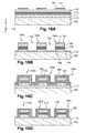
- FIGS. 16A to 16L schematically represent the steps of a method for producing the optoelectronic device 100, here an LED, according to the second embodiment. These figures represent cross sectional views of the structure forming the optoelectronic device 100.
- the stack of layers is made from which the mesa structures 124 of the LED 100 will be made.
- This stack comprises, in the direction from the upper face of the stack to the bottom face of the stack in contact with the substrate 102, a first p-doped semiconductor layer 115 (here comprising GaN), active layers 113 corresponding to an alternating stack of one or more quantum well emissive layers, comprising for example InGaN, and barrier layers, comprising for example GaN, a second n-doped semiconductor layer 111, for example comprising GaN, and the buffer layer 110, comprising, for example, n-doped GaN.
- a first p-doped semiconductor layer 115 here comprising GaN
- active layers 113 corresponding to an alternating stack of one or more quantum well emissive layers, comprising for example InGaN
- barrier layers comprising for example GaN
- a second n-doped semiconductor layer 111 for example comprising GaN
- the buffer layer 110 comprising, for
- the first electrodes 112 intended to form the anodes of the LED 100 are then produced on the first p-doped semiconductor layer 115, for example via a deposition and then a lithography and etching of a first layer of electrically conductive material, comprising for example aluminum.
- the first electrodes 112 each have a shape and dimensions, in the plane of the upper face of the first p-doped semiconductor layer 115 on which they are made, substantially similar to those desired for the mesa structures 124 of the LED 100 , and for example a disc-shaped section.
- a hard mask 131 is formed on the first layer of electrically conductive material intended to form the first electrodes 112 such that openings formed in this mask 131 correspond to the patterns to be etched in the stack of layers on which the hard mask 131 is formed so to define the first electrodes 112 and the mesa structures 124 of the LED 100.
- the portions of the hard mask 131 have a shape and dimensions, in the plane of the upper face of the first p-doped semiconductor layer 115 on which the first electrodes 112 are made substantially similar to those of the first electrodes 112.
- an etching of the first p-doped semiconductor layer 115, active layers 113 and a portion of the thickness of the second n-doped semiconductor layer 111 is also carried out according to the pattern defined by the hard mask 131, forming the mesa structures 124a, 124b and 124c, for example of cylindrical shape, each comprising the active zone 104 disposed between the first p-doped semiconductor portion 106 and the second n-doped semiconductor portion 108.
- This etching is stopped at a level of depth located in the second n-doped semiconductor layer 111 such that a portion 114 of this second layer 111 is kept at the bottom of each of the etched areas of the stack (on which the second electrodes 116).
- This etching step forms, around the mesa structures 124, empty spaces 133 which will subsequently be used for the production of the second electrodes 116, the dielectric passivation layer 120 and the grids 118.
- the etching implemented is a dry etching , for example a reactive ion etching with a plasma of Cl 2 . This engraving delimits the mesa structures 124.
- the hard mask 131 may be deleted or not before the implementation of the following steps.
- the etching of the electrodes 112 and that of the mesa structures 124 are preferably implemented during the same etching step.
- a first dielectric layer 121 comprising, for example, SiN or a high-k dielectric material according to the desired material to form the dielectric passivation layer 120, is then deposited with a thickness that is consistent, for example equal to 10 nm, over the portions of the hard mask 131 and along the walls of the empty spaces 133, thus covering the side walls of the first electrodes 112, the first p-doped semiconductor portions 106, the active zones 104 and the second n-doped semiconductor portions 108.
- This first dielectric layer 121 is also deposited on the non-etched portions 114 of the second n-doped semiconductor layer 111 forming the bottom walls of the void spaces 133.
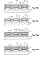
- a second layer of electrically conductive material 134 for forming the grids 118 for example of aluminum and having a thickness of about 500 nm, is then deposited in a conformal manner on the first dielectric layer 121.
- a second dielectric layer 136 comprising for example SiN or a high-k dielectric material and having a thickness equal to 100 nm, or more generally at least equal to 5 nm, is then deposited. on the second layer of electrically conductive material 134 ( figure 16C ).
- a directional etching of the second dielectric layer 136, via an SF 6 plasma, and the second layer of electrically conductive material 134, via a plasma of type Cl 2 argon, is then implemented such that remaining portions of the second dielectric layer 136 and the second layer of electrically conductive material 134 cover the side walls of the voids 133, that is to say the lateral flanks of the mesa structures 124 ( figure 16D ).
- the remaining portions of the second layer of electrically conductive material 134 form the grids 118 surrounding the mesa structures 124, and the remaining portions of the dielectric layers 121 and 136 form portions of the dielectric passivation layer 120.
- the dielectric layer 121 and the layer of electrically conductive material 134 are etched before the deposition of the second dielectric layer 136.
- the second dielectric layer 136 is then deposited, which makes it possible to surround the lower portions of the remaining portions of the the conductive layer 134 by dielectric, as shown in FIG. figure 16D .
- Another etching may then be implemented to form the accesses to the second n-doped semiconductor layer 111 between the mesa structures 124.
- a deposit of a third layer of electrically conductive material 138 is then made to fill the voids 133 ( figure 16E ). This deposit is made on the entire structure and also covers the mesa structures 124. This deposit is for example obtained via a deposit of a titanium layer of thickness equal to about 20 nm, and then a deposit of a layer aluminum thickness of about 11 microns.
- a chemical mechanical planarization is then implemented in order to remove the parts of the third layer 138 covering the mesa structures 124 and also to remove the portions of the passivation layer 120 covering the mesa structures 124.
- This CMP is set implemented by taking as the stop surface the upper faces of the first electrodes 112. The remaining portions of the layer 138 form the second electrodes 116.
- a deposit of a third dielectric layer 140 comprising, for example, SiN or a high-k dielectric, and having a thickness of about 100 nm, is then produced, this third dielectric layer 140 being then etched so that the remaining portions of this third dielectric layer 140 does not cover the grids 118 ( figure 16G ).
- a deposit of a fourth layer of electrically conductive material 142 is then made on the entire structure ( figure 16H ) in order to carry out, after an etching, the electrical contacts 119 on the grids 118 as well as the remote electrical contact 128 with respect to the mesa structures 124 and to which the grids 118 are connected via the electrical contacts 119.
- This electrically conductive material corresponds, for example to aluminum deposited on a thickness of about 100 nm.
- a fourth dielectric layer 143 (SiN or high-k dielectric) is deposited on the fourth layer of electrically conductive material 142, then this fourth dielectric layer 143 and the fourth layer of electrically conductive material 142 are etched so that remaining portions of the fourth layer of electrically conductive material 142 form the electrical contacts 119 arranged on the grids 118 and electrically connect the grids 118 to the remote contact 128, and that remaining portions of the fourth dielectric layer 143, forming part of the dielectric passivation layer 120, cover the electrical contacts 119.
- Parts of the third dielectric layer 140 covering the electrodes 112 and 116 are also etched to form accesses to the electrodes 112 and 116.
- a fifth layer of dielectric material 146 (SiN or high-k dielectric) is deposited over the entire structure, for example with a thickness equal to about 100 nm ( figure 16J ), then the portions of this fifth dielectric layer 146 covering the electrodes 112 and 116 are etched to form accesses to the electrodes 112 and 116 ( figure 16K ). Remaining portions of this fifth layer of dielectric material 146 overlap the side flanks of the electrical contacts 119 and form, along with the remaining portions of the other dielectric layers, the dielectric passivation layers 120 surrounding the grids 118 and the electrical contacts 119.
- the LED 100 is completed by depositing a fifth layer of electrically conductive material over the entire structure and implementing a CMP with stop on the dielectric passivation layers 120, thus forming metal portions extending the electrodes 112 and 116 to the same level as the dielectric passivation layers 120 ( figure 16L ).
- This last step of CMP can form, at the level of the upper face 122 substantially flat, the slight hollows at the level of the metal contacts with respect to the dielectric passivation layers 120.
- FIGS. 17A to 17F represent the steps of a process for producing the optoelectronic device 100, here an LED, according to the third embodiment previously described. These figures represent profile sectional views of the structure intended to form the LED 100.
- the stack of layers is made from which the mesa structure 124 of the LED 100 will be made.
- This stack is similar to that previously described in connection with the figure 16A .
- the first electrodes 112 and the hard mask 131 are made on the structure previously formed such that openings formed in this mask 131 correspond to the patterns to be etched in the layer stack on which the hard mask 131 is formed in order to define the locations in which the gate 118 will pass through the mesa structure 124 of the LED 100.
- an etching of the first p-doped semiconductor layer 115, the active layers 113 and the second n-doped semiconductor layer 111 and a portion of the thickness of the buffer layer 110 is then implemented. according to the pattern defined by the hard mask 131, forming in the mesa structure 124 of locations 148 in which the electrically conductive portions of the gate 118 are intended to pass through the mesa structure 124. This etching is also performed on the periphery of the mesa structure 124 to form the locations 150 at which the second electrode 116 will be realized. This etching is stopped at a depth level located in the buffer layer 110.
- this etching is stopped at another level, for example at the upper face of the buffer layer 110 or in the layer 111.
- the etching implemented is a dry etching, for example a reactive ion etching with a plasma of Cl 2 .
- the dielectric passivation layer 120 is then deposited in a conformal manner on the structure, that is to say both on the mesa structure 124 and in the locations 148 and 150 covering all the walls (side walls and walls background) of these locations ( figure 17C ).
- This dielectric passivation layer 120 is for example here HfO 2 deposited by ALD.
- the portions of the dielectric passivation layer 120 overlying the bottom walls 150 of the second electrode 116 locations are then etched, for example, via a type of plasma etching Cl 2 by masking the other portions of the dielectric passivation layer 120 to maintain , for example with resin ( figure 17D ).
- a deposit of a layer of electrically conductive material 152 full plate is then made, filling the locations 148 and 150 ( figure 17E ), then a CMP is implemented with a stop on the first electrodes 112, thus forming the second electrode 116 as well as the dielectric passivation layer 120.
- the pn or pin junction of the optoelectronic device 100 can be made from ZnO.
- a two-dimensional ZnO heterostructure comprising quantum wells of ZnCdO or ZnMgO can be first performed. P type implantation and annealing of this heterostructure can then be carried out, as described for example in the document FR 2 981090 A1 .
- the layer 115 corresponds to a p-doped ZnO layer (obtained for example by phosphorus implantation)
- the active layers 113 correspond to ZnO / ZnCdO or ZnO / ZnMgO wells
- the 111 layer corresponds to an n-doped ZnO layer. Steps analogous to those previously described in connection with the Figures 16B to 16L can then be implemented from such a stack to complete the embodiment of the device 100.
- each element comprising a gate and the passivation layer arranged around the gate and which makes it possible to ionize the dopants of the junction via a generation of an electric field in the junction can be replaced by one or more metal portions forming one or more Schottky contacts with the materials of the pn or pin junction.
- the metal portion or portions are directly in contact with the semiconductor materials of the junction, without insulating material disposed between the semiconductor materials and the metallic material.
- the metal used is selected from metals having a high output work, such as for example tungsten whose work output is equal to about 6.1 eV, or platinum.
- the choice of the metal used to form such Schottky contacts depends on the structure of the optoelectronic device 100, the semiconductor materials used, etc.
- the figure 18 represents an exemplary embodiment of such an optoelectronic device 100, here of similar structure to the device 100 previously described in connection with the figures 13 and 14 but in which the mesa structure 124 is traversed by metal portions 154 forming Schottky contacts with the semiconductor materials forming the pn junction.
- the junction of the optoelectronic device 100 is made on a diamond basis, for example in the case of an LED or a photodiode capable of producing a transmission or detection of UV light.
- the stack of layers from which such a device can be made can be formed from a naturally p-type graphite substrate. A p-type diamond growth is then performed, and then an n-type diamond layer is produced, for example as described in FIG. document S. Koizumi et al., "Growth and characterization of phosphorous doped ⁇ 111 ⁇ homoepitaxial diamond thin films", Appl. Phys. Lett.
- the grids or Schottky contacts are not used to ionize acceptors but to ionize donors in n-doped diamond and have a high activation energy.
- the gate or the Schottky contact or contacts are made such that they cover at least a portion of the lateral flanks of at least a portion of the doped semiconductor portion n located at the junction p-n. or p-i-n, which will be positively polarized (positive Vg voltage) in order to increase the internal quantum efficiency in the junction.
- the first semiconductor portion 106 is advantageously made with an n-type semiconductor.
- One or more LEDs 100 according to one of the various embodiments described above can be integrated within a light emitting device 1000.
- figure 19 schematically represents such a device 1000 comprising 9 LEDs 100 made on the same substrate 102 in the form of a 3 ⁇ 3 matrix.
- the reference 100 may correspond not to one or more LEDs, but to one or more photodiodes having pn or pin junctions.
- the LEDs the grids or Schottky contacts are used in this case to ionize the dopants (acceptors or donors) and thus adjust the doping in the junction used to perform the photoelectric conversion.
- a photodiode 100 for performing UV light detection if AlGaN is used to make the pn junction (for example, by MOCVD growth of n-type AlGaN with about 50% of aluminum doped with silicon at 10 19 donors / cm 3 over a thickness of about 11 ⁇ m then to 10 17 donors / cm 3 over a thickness of about 500 nm, then growth of p-type AlGaN p doped with magnesium at about 10 19 acceptors / cm 3 over a thickness of about 300 nm) the problem related to the high activation energy of the acceptors in the p-type semiconductor found in such a photodiode, limiting the performance for the detection of UV light.
- the use of an n-type semiconductor having a high donor activation energy is also possible for the production of a photodiode.
- the grids or Schottky contacts make it possible to ionize these donors in order to improve the conductivity of the n-type semiconductor.
- the device 1000 shown on the figure 19 may not correspond to a light emitting device but to a photodetector device comprising several photodiodes 100.
- the electrode or electrodes 112 at the top of the mesa structures are made from a material transparent to the wavelengths intended to be detected and converted photoelectrically, for example ITO with a thickness of about 100 nm.
- the second electrodes 116 serve in this case of electron collectors.
Abstract
Dispositif optoélectronique (100) comportant une structure mesa (124) comprenant : - une première (106) et une deuxième (108) portions de semi-conducteur formant une jonction p-n, - une première électrode (112) reliée électriquement à la première portion qui est disposée entre la deuxième portion et la première électrode, le dispositif comportant en outre: - une deuxième électrode (116) reliée électriquement à la deuxième portion, - un élément (118, 120) apte à ioniser des dopants de la première et/ou deuxième portion via une génération d'un champ électrique dans la première et/ou deuxième portion et recouvrant au moins une partie des flancs latéraux d'au moins une partie de la première et/ou de la deuxième portion de semi-conducteur et d'au moins une partie d'une zone de charge d'espace formée par les première et deuxième portions, des faces supérieures de la première électrode et de la deuxième électrode forment une surface continue sensiblement plane (122).An optoelectronic device (100) having a mesa structure (124) comprising: a first (106) and a second (108) semiconductor portion forming a p-n junction, a first electrode (112) electrically connected to the first portion which is arranged between the second portion and the first electrode, the device further comprising: a second electrode (116) electrically connected to the second portion, an element (118, 120) capable of ionizing dopants of the first and / or second portion via a generation of an electric field in the first and / or second portion and covering at least a portion of the lateral flanks of at least a portion of the first and / or second semiconductor portion and at least a portion of a space charge area formed by the first and second portions, upper faces of the first electrode and the second electrode form a substantially planar continuous surface (122).
Description
L'invention concerne le domaine des dispositifs optoélectroniques à jonction p-n tels que des diodes électroluminescentes (DELs ou LEDs ou micro-LEDs), utilisées notamment pour la réalisation de tout dispositif lumineux à base de LEDs (écrans, projecteurs, murs d'images, etc.), ou des dispositifs photodétecteurs tels que des photodiodes.The invention relates to the field of pn-type optoelectronic devices such as light-emitting diodes (LEDs or LEDs or micro-LEDs), used in particular for the production of any light-based device based on LEDs (screens, projectors, image walls, etc.), or photodetector devices such as photodiodes.
Une diode électroluminescente émettant une lumière bleue comprend généralement une jonction p-i-n à base de GaN comportant : une couche de GaN dopée p à typiquement 1019 accepteurs/cm3, une couche non intentionnellement dopée, ou intrinsèque, de GaN typiquement à 1017 donneurs/cm3 dans laquelle sont formés des puits quantiques d'InGaN, et une couche de GaN dopée n à 1019 donneurs/cm3. La couche non intentionnellement dopée et comprenant les puits quantiques dans lesquels se produit l'émission lumineuse est appelée zone active. Une couche de blocage d'électrons en AlGaN avec une concentration en aluminium comprise entre 8 % et 15 % et dopée p peut être rajoutée entre la zone active et la couche de GaN dopée p, comme décrit dans le document
Le principal problème limitant l'efficacité de ce type de diode électroluminescente est l'énergie d'activation élevée des accepteurs dans la couche de GaN dopée p, qui est typiquement de l'ordre de 200 meV.The main problem limiting the efficiency of this type of light-emitting diode is the high activation energy of the acceptors in the p-doped GaN layer, which is typically of the order of 200 meV.
Une diode électroluminescente émettant dans le domaine des UV (LED UV) peut être réalisée en utilisant de l'AlGaN pour former la jonction p-i-n, avec des puits quantiques en GaN. Plus la concentration en aluminium dans l'AlGaN augmente, plus l'énergie d'activation des accepteurs dans l'AlGaN dopé p augmente. A titre d'exemple, cette énergie d'activation est de l'ordre de 600 meV dans l'AIN. La quantité d'accepteurs activés dans l'AlGaN est alors extrêmement faible, limitant d'autant l'efficacité d'une telle LED UV.A UV emitting diode (UV LED) can be made using AlGaN to form the pin junction, with GaN quantum wells. The higher the aluminum concentration in AlGaN increases, the more the activation energy of the acceptors in the p-doped AlGaN increases. For example, this activation energy is of the order of 600 meV in the AIN. The quantity of acceptors activated in the AlGaN is then extremely low, thus limiting the effectiveness of such a UV LED.
Pour réduire l'énergie d'activation des accepteurs dans cette LED UV, du GaN dopé p peut être utilisé à la place de l'AlGaN dopé p. Cela a par contre comme inconvénient de limiter l'efficacité radiative dans la zone active de la LED UV qui est en AlGaN. De plus, une partie de la lumière UV émise par la zone active est absorbée par le GaN dopé p.To reduce the activation energy of the acceptors in this UV LED, p-doped GaN can be used in place of p-doped AlGaN. However, this has the disadvantage of limiting the radiative efficiency in the active zone of the UV LED which is in AlGaN. In addition, a part of the UV light emitted by the active zone is absorbed by the p-doped GaN.
Dans les exemples décrits ci-dessus, les limitations observées sont dues à l'énergie d'activation élevée des accepteurs dans la jonction p-n. Il est également possible de rencontrer des problèmes analogues liés à une énergie d'activation élevée des donneurs lorsqu'ils sont profonds. Par exemple, ces problèmes se retrouvent dans le cas de LEDs dont les jonctions p-n sont réalisées en diamant car dans ce cas, les donneurs ont une forte énergie d'ionisation (de l'ordre de 460 meV).In the examples described above, the limitations observed are due to the high activation energy of the acceptors in the p-n junction. It is also possible to encounter similar problems related to a high activation energy of the donors when they are deep. For example, these problems are found in the case of LEDs whose p-n junctions are made of diamond because in this case, the donors have a high ionization energy (of the order of 460 meV).
De plus, les problèmes exposés ci-dessus se retrouvent également de manière analogue pour des photodiodes, par exemple celles destinées à réaliser une détection de lumière UV et réalisées à partir d'AlGaN ou de diamant.In addition, the problems described above are also found analogously for photodiodes, for example those intended to perform UV light detection and made from AlGaN or diamond.
Un but de la présente invention est de proposer un nouveau type de dispositif optoélectronique à jonction p-n, par exemple une diode électroluminescente ou une photodiode, dont l'efficacité d'émission ou de détection, ou efficacité quantique interne, est améliorée par rapport aux dispositifs optoélectroniques à jonction p-n de l'art antérieur, notamment pour des matériaux semi-conducteurs présentant des énergies d'activation d'accepteurs ou de donneurs élevées.An object of the present invention is to propose a new type of pn-junction optoelectronic device, for example a light-emitting diode or a photodiode, whose emission or detection efficiency, or internal quantum efficiency, is improved compared to the devices. Prior art pn junction optoelectronic devices, especially for semiconductor materials having high acceptor or donor activation energies.
Pour cela, la présente invention propose un dispositif optoélectronique comportant au moins une structure mesa comprenant au moins :
- une première et une deuxième portions de semi-conducteur, l'une étant dopée p et l'autre étant dopée n, et formant ensemble une jonction p-n,
- une première électrode reliée électriquement à la première portion de semi-conducteur qui est disposée entre la deuxième portion de semi-conducteur et la première électrode,
le dispositif optoélectronique comportant en outre au moins : - une deuxième électrode reliée électriquement à la deuxième portion de semi-conducteur,
- un élément apte à ioniser des dopants de la jonction p-n, ou plus précisément apte à ioniser des dopants de la première et/ou deuxième portion de semi-conducteur, via une génération d'un champ électrique dans la jonction p-n, ou plus précisément dans la première et/ou deuxième portion de semi-conducteur, et recouvrant au moins une partie des flancs latéraux d'au moins une partie de la première et/ou de la deuxième portion de semi-conducteur localisée au niveau de la jonction p-n, ou plus précisément au moins une partie de la première et/ou de la deuxième portion de semi-conducteur et au moins une partie d'une zone de charge d'espace formée par les première et deuxième portions de semi-conducteur,
et dans lequel des faces supérieures d'au moins la première électrode et de la deuxième électrode forment une surface continue sensiblement plane.
- first and second semiconductor portions, one being p-doped and the other being n-doped, and together forming a pn junction,
- a first electrode electrically connected to the first semiconductor portion which is disposed between the second semiconductor portion and the first electrode,
the optoelectronic device further comprising at least: - a second electrode electrically connected to the second semiconductor portion,
- an element capable of ionizing dopants of the pn junction, or more precisely capable of ionizing dopants of the first and / or second semiconductor portion, via a generation of an electric field in the pn junction, or more precisely in FIG. the first and / or second semiconductor portion, and covering at least a portion of the lateral flanks of at least a portion of the first and / or second semiconductor portion located at the pn junction, or more specifically at least a portion of the first and / or second semiconductor portion and at least a portion of a space charge region formed by the first and second semiconductor portions,
and wherein upper faces of at least the first electrode and the second electrode form a substantially planar continuous surface.
La présence de l'élément apte à ioniser des dopants de la jonction p-n, ou apte à ioniser des dopants de la première et/ou deuxième portion de semi-conducteur, à proximité du semi-conducteur dopé p ou n du dispositif optoélectronique permet la génération d'un champ électrique améliorant la conductivité du semi-conducteur dopé p ou n. Cet effet de champ entraîne une ionisation des dopants dans ce semi-conducteur (ionisation des accepteurs pour du semi-conducteur dopé p ou ionisation des donneurs pour du semi-conducteur dopé n), ce qui permet d'augmenter l'efficacité quantique interne, c'est-à-dire l'efficacité d'émission ou de réception, du dispositif optoélectronique car par exemple un plus grand nombre d'accepteurs (trous) sont disponibles pour se recombiner avec les donneurs (électrons) provenant du semi-conducteur dopé n du dispositif notamment lorsque le semi-conducteur dopé p a une énergie d'activation des accepteurs élevée, ou bien un plus grand nombre de donneurs sont disponibles pour se recombiner avec les accepteurs du semi-conducteur dopé p notamment lorsque le semi-conducteur dopé n a une énergie d'activation des donneurs élevée.The presence of the element capable of ionizing dopants of the pn junction, or capable of ionizing dopants of the first and / or second semiconductor portion, in the vicinity of the doped semiconductor p or n of the optoelectronic device allows the generating an electric field improving the conductivity of the p-doped or n-doped semiconductor. This field effect causes an ionization of the dopants in this semiconductor (ionization of the acceptors for p-doped semiconductor or ionization of the donors for n-doped semiconductor), which makes it possible to increase the internal quantum efficiency, that is to say, the emission or reception efficiency of the optoelectronic device because, for example, a larger number of acceptors (holes) are available to recombine with the donors (electrons) coming from the doped semiconductor n of the device, especially when the semiconductor doped with a high acceptor activation energy, or a larger number of donors are available to recombine with the acceptors of the p-doped semiconductor especially when the doped semiconductor has a high donor activation energy.
Le dispositif optoélectronique peut comporter avantageusement un ou des semi-conducteurs ayant des énergies d'activation d'accepteurs importantes, par exemple supérieures ou égales à environ 50 meV, tels que du GaN (dont la valeur de l'énergie d'ionisation des accepteurs est d'environ 200 meV) et des puits quantiques en InGaN (dont la valeur de l'énergie d'ionisation varie en fonction de la concentration d'indium et est comprise entre environ 50 meV et 200 meV), par exemple pour la réalisation d'une diode électroluminescente émettant une lumière de couleur bleu, ou de l'AlGaN (dont la valeur de l'énergie d'ionisation des accepteurs est supérieure à environ 200 meV), ou de l'AIN (dont la valeur de l'énergie d'ionisation des accepteurs est égale à environ 600 meV), et des puits quantiques en GaN ou en AlGaN, par exemple pour la réalisation d'une diode électroluminescente émettant une lumière UV ou d'une photodiodes réalisant une détection de lumière UV. Il est également possible que l'InGaN soit utilisé en tant que matériau semi-conducteur de type p pour certaines diodes électroluminescentes.The optoelectronic device may advantageously comprise one or more semiconductors having significant acceptor activation energies, for example greater than or equal to approximately 50 meV, such as GaN (whose value of the ionization energy of the acceptors is about 200 meV) and InGaN quantum wells (whose value of the ionization energy varies as a function of the indium concentration and is between about 50 meV and 200 meV), for example for the realization a light-emitting diode emitting a blue-colored light, or AlGaN (whose value of the ionization energy of the acceptors is greater than about 200 meV), or AIN (whose value of the ionization energy of acceptors is equal to about 600 meV), and quantum wells in GaN or AlGaN, for example for producing a light emitting diode emitting a UV light or a photodiodes performing UV light detection. It is also possible that InGaN is used as a p-type semiconductor material for some light-emitting diodes.
Il est également possible que le dispositif optoélectronique comporte un ou des semi-conducteurs ayant des énergies d'activation de donneurs importantes, par exemple supérieures ou égales à environ 50 meV tel que du diamant (dont la valeur de l'énergie d'ionisation des donneurs est d'environ 460 meV), par exemple pour la réalisation d'une diode électroluminescente ou d'une photodiode fonctionnant dans le domaine UV.It is also possible that the optoelectronic device comprises one or more semiconductors having energies of activation of important donors, for example greater than or equal to about 50 meV such as diamond (the value of the ionization energy of donors is approximately 460 meV), for example for producing a light emitting diode or a photodiode operating in the UV range.
La forte intégration des éléments d'un tel dispositif optoélectronique a pour avantage de minimiser les densités de courant obtenues dans les électrodes, et donc de réduire l'échauffement par effet Joule au sein du dispositif.The strong integration of the elements of such an optoelectronic device has the advantage of minimizing the current densities obtained in the electrodes, and therefore of reducing Joule heating in the device.
L'expression « structure mesa » désigne le fait que le dispositif optoélectronique est réalisé sous la forme d'un empilement de la première et de la deuxième portions de semi-conducteur dopées, une zone de jonction étant présente entre ces deux portions de semi-conducteur dopées, et que cet empilement est gravé sur au moins une partie de sa hauteur sous forme d'îlot appelé mesa et pouvant former des plots de toute forme comportant un tel empilement.The expression "mesa structure" designates the fact that the optoelectronic device is made in the form of a stack of the first and second doped semiconductor portions, a junction zone being present between these two semiconductor portions. doped conductor, and that this stack is engraved on at least a portion of its height as an island called mesa and can form pads of any shape having such a stack.
De plus, la surface continue sensiblement plane formée par au moins les faces supérieures des électrodes du dispositif permet d'hybrider facilement, par exemple sans faire appel à des inserts tels que des microbilles de connexion, le dispositif à un autre élément, tel qu'un circuit électronique pouvant comporter également une face plane au niveau de laquelle se trouve des matériaux analogues à ceux du dispositif, par exemple par collage direct.In addition, the substantially planar continuous surface formed by at least the upper faces of the electrodes of the device makes it easy to hybridize, for example without using inserts such as connection microbeads, the device to another element, such as an electronic circuit may also include a flat face at which there are similar materials to those of the device, for example by direct bonding.
Les faces supérieures des électrodes forment une surface continue sensiblement plane, c'est-à-dire sont disposées sensiblement dans un même plan. L'expression « sensiblement plane » est ici utilisée pour désigner le fait que la surface formée par ces faces supérieures peut présenter des variations de hauteur, ou d'épaisseur, comprises entre 0 et environ 150 nm.The upper faces of the electrodes form a substantially flat continuous surface, that is to say are arranged substantially in the same plane. The term "substantially planar" is used here to designate the fact that the surface formed by these upper faces may have variations in height, or thickness, between 0 and about 150 nm.
Le terme « jonction p-n » utilisé ici désigne également une jonction de type p-i-n.The term "p-n junction" as used herein also refers to a p-i-n junction.
La zone de charge d'espace, ou zone de déplétion, correspond à la région qui apparait dans la jonction P-N, entre la portion dopée N et la portion dopée P et qui est dépourvue de porteurs libres.The space charge area, or depletion zone, corresponds to the region appearing in the P-N junction between the N-doped portion and the P-doped portion and which is devoid of free carriers.
L'élément apte à ioniser des dopants de la jonction p-n peut comporter :
- au moins une couche de passivation diélectrique recouvrant ladite au moins une partie des flancs latéraux d'au moins une partie de la première et/ou de la deuxième portion de semi-conducteur localisée au niveau de la jonction p-n et au moins une grille électriquement conductrice telle que la couche de passivation diélectrique soit disposée entre la grille et ladite au moins une partie de la première et/ou de la deuxième portion de semi-conducteur, et/ou
- au moins une portion métallique recouvrant ladite au moins une partie des flancs latéraux d'au moins une partie de la première et/ou de la deuxième portion de semi-conducteur localisée au niveau de la jonction p-n et formant un contact Schottky avec ladite au moins une partie de la première et/ou de la deuxième portion de semi-conducteur.
- at least one dielectric passivation layer covering said at least a portion of the lateral flanks of at least a portion of the first and / or second semiconductor portion located at the pn junction and at least one electrically conductive gate such that the dielectric passivation layer is disposed between the gate and the at least a portion of the first and / or second semiconductor portion, and / or
- at least one metal portion covering said at least a portion of the lateral flanks of at least a portion of the first and / or second semiconductor portion located at the pn junction and forming a Schottky contact with said at least one a portion of the first and / or second semiconductor portion.
L'élément apte à ioniser des dopants de la première et/ou deuxième portion de semi-conducteur peut comporter :
- au moins une couche de passivation diélectrique recouvrant ladite au moins une partie des flancs latéraux d'au moins une partie de la première et/ou de la deuxième portion de semi-conducteur et d'au moins une partie de la zone de charge d'espace, et au moins une grille électriquement conductrice telle que la couche de passivation diélectrique soit disposée entre la grille et ladite au moins une partie de la première et/ou de la deuxième portion de semi-conducteur et entre la grille et ladite au moins une partie de la zone de charge d'espace, et/ou
- au moins une portion métallique recouvrant ladite au moins une partie des flancs latéraux d'au moins une partie de la première et/ou de la deuxième portion de semi-conducteur et d'au moins une partie de la zone de charge d'espace et formant un contact Schottky avec ladite au moins une partie de la première et/ou de la deuxième portion de semi-conducteur et avec ladite au moins une partie de la zone de charge d'espace.
- at least one dielectric passivation layer covering said at least a portion of the lateral flanks of at least a portion of the first and / or second semiconductor portion and at least a portion of the charging zone of space, and at least one electrically conductive gate such as the dielectric passivation layer is disposed between the gate and said at least a portion of the first and / or second semiconductor portion and between the gate and said at least one part of the space charge area, and / or
- at least one metal portion covering said at least a portion of the lateral flanks of at least a portion of the first and / or second semiconductor portion and at least a portion of the space charge area and forming a Schottky contact with said at least a portion of the first and / or second semiconductor portion and with said at least a portion of the space charge area.
Dans ce cas, le dispositif optoélectronique peut être tel que :
- une première partie de la couche de passivation diélectrique entoure latéralement au moins en partie la première électrode, la première portion de semi-conducteur et au moins une partie de la deuxième portion de semi-conducteur,
- la grille recouvre latéralement la première partie de la couche de passivation diélectrique,
- une deuxième partie de la couche de passivation diélectrique recouvre latéralement la grille (la grille pouvant être disposée entre la première et la deuxième parties de la couche de passivation diélectrique), et
- la deuxième électrode recouvre latéralement la deuxième partie de la couche de passivation diélectrique,
ou le dispositif optoélectronique peut être tel que : - la portion métallique entoure latéralement au moins en partie la première électrode, la première portion de semi-conducteur et au moins une partie de la deuxième portion de semi-conducteur, et
- la deuxième électrode recouvre latéralement la portion métallique.
- a first portion of the dielectric passivation layer laterally surrounds at least a portion of the first electrode, the first semiconductor portion, and at least a portion of the second semiconductor portion,
- the grid laterally covers the first part of the dielectric passivation layer,
- a second portion of the dielectric passivation layer laterally covers the gate (the gate being able to be arranged between the first and second portions of the dielectric passivation layer), and
- the second electrode laterally covers the second part of the dielectric passivation layer,
or the optoelectronic device may be such that: - the metal portion laterally surrounds at least part of the first electrode, the first semiconductor portion and at least a portion of the second semiconductor portion, and
- the second electrode laterally covers the metal portion.
Dans ce cas, la surface continue sensiblement plane peut être formée par les faces supérieures des électrodes, de la grille et de la couche de passivation diélectrique, ou bien par les faces supérieures des électrodes et de la portion métallique. Des légères variations de hauteur ou d'épaisseur peuvent avoir pour origine la mise en oeuvre d'une planarisation mécano-chimique (CMP) mise en oeuvre en présence des matériaux des électrodes, de la grille et de la couche de passivation diélectrique, les vitesses de gravure des matériaux conducteurs des électrodes (et éventuellement de la grille lorsque celle-ci est exposée au niveau de la face supérieure du dispositif) étant différentes par rapport à celle du matériau diélectrique de la couche de passivation. Ces légères variations de hauteur ou d'épaisseur, entre les faces supérieures de la couche de passivation diélectrique et celles des électrodes, peuvent avoir pour avantage de garantir une excellente isolation entre les électrodes du dispositif et/ou vis-à-vis de la grille et/ou d'électrodes ou de grilles de diodes adjacentes lorsque des creux se situent au niveau des faces supérieures des électrodes et/ou de la grille.In this case, the substantially planar continuous surface may be formed by the upper faces of the electrodes, the gate and the dielectric passivation layer, or by the upper faces of the electrodes and the metal portion. Slight variations in height or thickness may be due to the implementation of a chemical mechanical planarization (CMP) implemented in the presence of the electrode materials, the gate and the dielectric passivation layer, the speeds etching conductive materials of the electrodes (and possibly the gate when the latter is exposed at the upper face of the device) being different from that of the dielectric material of the passivation layer. These slight variations in height or thickness, between the upper faces of the dielectric passivation layer and those of the electrodes, may have the advantage of guaranteeing excellent insulation between the electrodes of the device and / or with respect to the gate and / or adjacent diode electrodes or grids when depressions are located at the upper faces of the electrodes and / or the gate.
Le dispositif optoélectronique peut comporter :
- plusieurs structures mesa,
- plusieurs couches de passivation diélectriques recouvrant chacune au moins une partie des flancs latéraux d'au moins une partie de la première et/ou de la deuxième portion de semi-conducteur localisée au niveau de la jonction p-n d'une des structures mesa, c'est-à-dire au moins une partie des flancs latéraux d'au moins une partie de la première et/ou de la deuxième portion de semi-conducteur et d'au moins une partie de la zone de charge d'espace d'une des structures mesa, et plusieurs grilles électriquement conductrices telles que chaque couche de passivation diélectrique est disposée entre l'une des grilles et ladite au moins une partie de la première et/ou de la deuxième portion de semi-conducteur d'une des structures mesa et entre l'une des grilles et ladite au moins une partie de la zone de charge d'espace d'une des structures mesa, ou plusieurs portions métalliques recouvrant chacune au moins une partie des flancs latéraux d'au moins une partie de la première et/ou de la deuxième portion de semi-conducteur localisée au niveau de la jonction p-n d'une des structures mesa, c'est-à-dire au moins une partie des flancs latéraux d'au moins une partie de la première et/ou de la deuxième portion de semi-conducteur et d'au moins une partie de la zone de charge d'espace d'une des structures mesa,
- several mesa structures,
- a plurality of dielectric passivation layers each covering at least a portion of the lateral flanks of at least a portion of the first and / or second semiconductor portion located at the pn junction of one of the mesa, c 'structures; that is at least a portion of the lateral flanks of at least a portion of the first and / or second semiconductor portion and at least a portion of the space charge area of a mesa structures, and several electrically conductive grids such that each dielectric passivation layer is disposed between one of the grids and said at least a portion of the first and / or second semiconductor portion of one of the mesa structures. and between one of the grids and said at least a portion of the space charge area of one of the mesa structures, or a plurality of metal portions each covering at least a portion of the side flanks of at least a portion of the first and or of the second semiconductor portion located at the pn junction of one of the mesa structures, that is to say at least a portion of the side flanks of at least a portion of the first and / or second semiconductor portion and at least a portion of the space charge area of one of the mesa structures,
Dans ce cas :
- chacune des structures mesa peut être entourée latéralement au moins en partie par une première partie d'une des couches de passivation diélectriques,
- chacune des grilles peut recouvrir latéralement la première partie d'une des couches de passivation diélectriques,
- une deuxième partie de chacune des couches de passivation diélectriques peut recouvrir latéralement l'une des grilles (qui est donc disposée entre la première et la deuxième partie d'une des couches de passivation diélectriques), et
- la deuxième électrode peut recouvrir latéralement les deuxièmes parties des couches de passivation diélectriques,
ou bien : - chacune des structures mesa peut être entourée latéralement au moins en partie par une des portions métalliques, et
- la deuxième électrode peut recouvrir latéralement les portions métalliques.
- each of the mesa structures may be laterally surrounded at least in part by a first part of one of the dielectric passivation layers,
- each of the grids can laterally cover the first part of one of the dielectric passivation layers,
- a second part of each of the dielectric passivation layers can laterally cover one of the grids (which is therefore arranged between the first and the second part of one of the dielectric passivation layers), and
- the second electrode can laterally cover the second portions of the dielectric passivation layers,
or : - each of the mesa structures may be laterally surrounded at least in part by one of the metal portions, and
- the second electrode can laterally cover the metal portions.
En variante :
- la grille peut comporter au moins une portion d'au moins un matériau électriquement conducteur s'étendant dans la structure mesa, ou la portion métallique peut s'étendre dans la structure mesa, et
- la deuxième électrode peut être disposée autour de la structure mesa.
- the grid may comprise at least a portion of at least one electrically conductive material extending in the mesa structure, or the metal portion may extend in the mesa structure, and
- the second electrode can be arranged around the mesa structure.
Le dispositif optoélectronique peut comporter plusieurs structures mesa, et :
- la grille peut comporter plusieurs portions d'au moins un matériau électriquement conducteur s'étendant dans une ou plusieurs des structures mesa, ou plusieurs portions métalliques peuvent s'étendre dans une ou plusieurs des structures mesa, et
- la deuxième électrode peut être disposée autour de la ou de chacune des structures mesa.
- the grid may comprise several portions of at least one electrically conductive material extending in one or more of the mesa structures, or a plurality of metal portions may extend into one or more of the mesa structures, and
- the second electrode may be arranged around the or each of the mesa structures.
Le dispositif optoélectronique peut comporter en outre un contact électrique disposé à côté de la ou des structures mesa et de la deuxième électrode, et auquel la ou les grilles ou la ou les portions métalliques sont reliées électriquement.The optoelectronic device may further comprise an electrical contact disposed next to the mesa structure (s) and the second electrode, and to which the at least one grid or the metal portion or portions are electrically connected.
La surface continue sensiblement plane peut être formée en outre par une ou des faces supérieures de la ou des grilles ou de la ou des portions métalliques, et/ou par des faces supérieures de la ou des couches de passivation diélectriques, et/ou la ou chacune des couches de passivation diélectriques peut recouvrir une face supérieure de la ou de chacune des grilles.The substantially planar continuous surface may be further formed by one or more upper faces of the at least one grid or metal portion (s), and / or upper faces of the dielectric passivation layer (s), and / or the each of the dielectric passivation layers may cover an upper face of the or each of the grids.
La couche de passivation diélectrique peut recouvrir une face supérieure de la grille.The dielectric passivation layer may cover an upper face of the gate.
Le dispositif optoélectronique peut comporter en outre au moins une couche tampon comportant un semi-conducteur dopé selon le même type de conductivité que la deuxième portion de semi-conducteur et sur laquelle sont disposées la deuxième portion de semi-conducteur et la deuxième électrode l'une à côté de l'autre.The optoelectronic device may further comprise at least one buffer layer comprising a semiconductor doped according to the same type of conductivity as the second semiconductor portion and on which the second semiconductor portion and the second electrode electrode are disposed. one next to the other.
Le dispositif optoélectronique peut comporter en outre une deuxième couche de semi-conducteur dopée comportant une face supérieure structurée dont une première partie saillante forme la deuxième portion de semi-conducteur, et la deuxième électrode peut être disposée sur au moins une deuxième partie de la deuxième couche de semi-conducteur dopée formant un creux de la face structurée de la deuxième couche de semi-conducteur dopée.The optoelectronic device may further comprise a second doped semiconductor layer having a structured upper face, a first protruding portion of which forms the second semiconductor portion, and the second electrode may be disposed on at least a second portion of the second semiconductor portion. doped semiconductor layer forming a hollow of the structured face of the second doped semiconductor layer.
En variante, une première partie de la deuxième portion de semi-conducteur disposée entre une deuxième partie de la deuxième portion de semi-conducteur et la première portion de semi-conducteur peut former un décrochement par rapport à la deuxième partie de la deuxième portion de semi-conducteur, et la deuxième électrode peut être reliée électriquement à la deuxième portion de semi-conducteur au niveau d'une face supérieure de la deuxième partie de la deuxième portion de semi-conducteur.Alternatively, a first portion of the second semiconductor portion disposed between a second portion of the second semiconductor portion and the first semiconductor portion may form a setback relative to the second portion of the second portion of the semiconductor portion. semiconductor, and the second The electrode may be electrically connected to the second semiconductor portion at an upper face of the second portion of the second semiconductor portion.
La première portion de semi-conducteur peut être dopée p et peut comporter au moins un semi-conducteur dont une énergie d'activation des accepteurs est supérieure ou égale à environ 200 meV, ou la première portion de semi-conducteur peut être dopée n et peut comporter au moins un semi-conducteur dont une énergie d'activation des donneurs est supérieure ou égale à environ 200 meV.The first semiconductor portion may be p-doped and may include at least one semiconductor having an acceptor activation energy of greater than or equal to about 200 meV, or the first semiconductor portion may be n-doped and may comprise at least one semiconductor having a donor activation energy of greater than or equal to about 200 meV.
L'invention concerne également un dispositif électronique comportant un ou plusieurs dispositifs optoélectroniques tels que décrits ci-dessus et correspondant à une ou plusieurs diodes électroluminescentes et/ou une ou plusieurs photodiodes.The invention also relates to an electronic device comprising one or more optoelectronic devices as described above and corresponding to one or more electroluminescent diodes and / or one or more photodiodes.
L'invention concerne également un procédé d'émission lumineuse à partir d'un dispositif optoélectronique tel que décrit ci-dessus, comportant la mise en oeuvre d'une polarisation du dispositif optoélectronique par l'application d'une tension électrique entre la ou les premières électrodes et la deuxième électrode du dispositif optoélectronique, et :
- l'application d'une différence de potentiels électriques entre la ou les grilles ou portions métalliques et la ou les électrodes reliées électriquement à la ou aux portions de semi-conducteur dopées p telle que le potentiel électrique appliqué sur la ou les grilles ou portions métalliques est inférieur ou égal au potentiel électrique appliqué sur la ou les électrodes reliées électriquement à la ou aux portions de semi-conducteur dopées p, ou
- l'application d'une différence de potentiels électriques entre la ou les grilles ou portions métalliques et la ou les électrodes reliées électriquement à la ou aux portions de semi-conducteur dopées n telle que le potentiel électrique appliqué sur la ou les grilles ou portions métalliques est supérieur ou égal au potentiel électrique appliqué sur la ou les électrodes reliées électriquement à la ou aux portions de semi-conducteur dopées n.
- applying a difference in electrical potentials between the one or more grids or metal portions and the one or more electrodes electrically connected to the p-doped semiconductor portion or portions such that the electrical potential applied to the grids or metal portions is less than or equal to the electrical potential applied to the electrode or electrodes electrically connected to the p-doped semiconductor portion or portions, or
- applying a difference in electrical potentials between the one or more grids or metal portions and the one or more electrodes electrically connected to the doped semiconductor portion or portions, such that the electrical potential applied to the grids or metal portions is greater than or equal to the electrical potential applied to the electrode or electrodes electrically connected to the n-doped semiconductor portion (s).
L'invention concerne également un procédé de conversion photoélectrique à partir d'un dispositif optoélectronique tel que décrit ci-dessus, comportant :
- l'application d'une différence de potentiels électriques entre la ou les grilles ou portions métalliques et la ou les électrodes reliées électriquement à la ou aux portions de semi-conducteur dopées p telle que le potentiel électrique appliqué sur la ou les grilles ou portions métalliques est inférieur ou égal au potentiel électrique appliqué sur la ou les électrodes reliées électriquement à la ou aux portions de semi-conducteur dopées p, ou
- l'application d'une différence de potentiels électriques entre la ou les grilles ou portions métalliques et la ou les électrodes reliées électriquement à la ou aux portions de semi-conducteur dopées n telle que le potentiel électrique appliqué sur la ou les grilles ou portions métalliques est supérieur ou égal au potentiel électrique appliqué sur la ou les électrodes reliées électriquement à la ou aux portions de semi-conducteur dopées n.
- applying a difference in electrical potentials between the one or more grids or metal portions and the one or more electrodes electrically connected to the p-doped semiconductor portion or portions such that the electrical potential applied to the grids or metal portions is less than or equal to the electrical potential applied to the electrode or electrodes electrically connected to the p-doped semiconductor portion or portions, or
- applying a difference in electrical potentials between the one or more grids or metal portions and the one or more electrodes electrically connected to the doped semiconductor portion or portions, such that the electrical potential applied to the grids or metal portions is greater than or equal to the electrical potential applied to the electrode or electrodes electrically connected to the n-doped semiconductor portion (s).
L'invention concerne également un procédé de réalisation d'un dispositif optoélectronique comportant au moins les étapes de :
- réalisation d'un empilement de couches comprenant au moins une première couche de semi-conducteur disposée entre une deuxième couche de semi-conducteur et une couche électriquement conductrice, l'une de la première et de la deuxième couche de semi-conducteur étant dopée p et l'autre de la première et de la deuxième couche de semi-conducteur étant dopée n,
- gravure de l'empilement de couches, réalisant au moins une structure mesa comprenant une première et une deuxième portions de semi-conducteur formant une jonction p-n et une première électrode reliée électriquement à la première portion de semi-conducteur,
- réalisation d'un élément apte à ioniser des dopants de la jonction p-n, ou apte à ioniser des dopants de la première et/ou deuxième portion de semi-conducteur, via une génération d'un champ électrique dans la jonction p-n, ou dans la première et/ou deuxième portion de semi-conducteur et recouvrant au moins une partie des flancs latéraux d'au moins une partie de la première et/ou de la deuxième portion de semi-conducteur localisée au niveau de la jonction p-n, c'est-à-dire au moins une partie des flancs latéraux d'au moins une partie de la première et/ou de la deuxième portion de semi-conducteur et d'au moins une partie d'une zone de charge d'espace formée par les première et deuxième portions de semi-conducteur,
- réalisation d'une deuxième électrode reliée électriquement à la deuxième portion de semi-conducteur,
- performing a stack of layers comprising at least a first semiconductor layer disposed between a second semiconductor layer and an electrically conductive layer, one of the first and second semiconductor layers being p-doped and the other of the first and second semiconductor layers being n-doped,
- etching the stack of layers, providing at least one mesa structure comprising a first and a second semiconductor portion forming a pn junction and a first electrode electrically connected to the first semiconductor portion,
- producing an element capable of ionizing dopants of the pn junction, or capable of ionizing dopants of the first and / or second semiconductor portion, via a generation of an electric field in the pn junction, or in the first and / or second semiconductor portion and covering at least a portion side flanks of at least a portion of the first and / or second semiconductor portion located at the pn junction, i.e. at least a portion of the side flanks of at least one part of the first and / or second semiconductor portion and at least a portion of a space charge area formed by the first and second semiconductor portions,
- producing a second electrode electrically connected to the second semiconductor portion,
Un tel procédé a pour avantage, en plus de ceux obtenus grâce à la présence de l'élément apte à ioniser des dopants de la jonction p-n, de nécessiter un nombre limité d'étapes pour sa mise en oeuvre.Such a method has the advantage, in addition to those obtained by virtue of the presence of the element capable of ionizing dopants of the p-n junction, of requiring a limited number of steps for its implementation.
Il est également décrit un procédé de réalisation d'un dispositif électronique, comportant la mise en oeuvre d'un procédé de réalisation d'au moins un dispositif optoélectronique tel que décrit ci-dessus.There is also described a method of producing an electronic device, comprising the implementation of a method for producing at least one optoelectronic device as described above.
La présente invention sera mieux comprise à la lecture de la description d'exemples de réalisation donnés à titre purement indicatif et nullement limitatif en faisant référence aux dessins annexés sur lesquels :
- la
figure 1 représente schématiquement un dispositif optoélectronique, objet de la présente invention, selon un premier mode de réalisation ; - la
figure 2 représente schématiquement le phénomène de courbure de bandes se produisant dans une diode électroluminescente selon l'invention ; - les
figures 3 à 9 représentent l'efficacité quantique interne obtenue en fonction de la densité de courant dans différentes diodes électroluminescentes, objets de la présente invention, pour différentes valeurs d'une différence de potentiels entre la grille et l'anode de ces diodes électroluminescentes ; - les
figures 10 et 11 représentent schématiquement un dispositif optoélectronique, objet de la présente invention, selon un deuxième mode de réalisation ; - la
figure 12 représente schématiquement un dispositif optoélectronique, objet de la présente invention, selon une variante du deuxième mode de réalisation ; - les
figures 13 et14 représentent schématiquement un dispositif optoélectronique, objet de la présente invention, selon un troisième mode de réalisation ; - la
figure 15 représente schématiquement un dispositif optoélectronique, objet de la présente invention, selon une variante du troisième mode de réalisation ; - les
figures 16A à 16L représentent schématiquement des étapes d'un procédé de réalisation d'un dispositif optoélectronique, objet de la présente invention, selon le deuxième mode de réalisation ; - les
figures 17A à 17F représentent schématiquement des étapes d'un procédé de réalisation d'un dispositif optoélectronique, objet de la présente invention, selon le troisième mode de réalisation ; - la
figure 18 représente schématiquement un dispositif optoélectronique, objet de la présente invention, selon une variante de réalisation ; - la
figure 19 représente schématiquement un dispositif électronique, objet de la présente invention, comportant plusieurs dispositifs optoélectroniques, également objets de la présente invention.
- the
figure 1 schematically represents an optoelectronic device, object of the present invention, according to a first embodiment; - the
figure 2 schematically represents the phenomenon of band curvature occurring in a light emitting diode according to the invention; - the
Figures 3 to 9 represent the internal quantum efficiency obtained as a function of the current density in different light-emitting diodes, objects of the present invention, for different values of a potential difference between the gate and the anode of these light-emitting diodes; - the
Figures 10 and 11 schematically represent an optoelectronic device, object of the present invention, according to a second embodiment; - the
figure 12 schematically represents an optoelectronic device, object of the present invention, according to a variant of the second embodiment; - the
figures 13 and14 schematically represent an optoelectronic device, object of the present invention, according to a third embodiment; - the
figure 15 schematically represents an optoelectronic device, object of the present invention, according to a variant of the third embodiment; - the
Figures 16A to 16L schematically represent steps of a method for producing an optoelectronic device, object of the present invention, according to the second embodiment; - the
Figures 17A to 17F schematically represent steps of a method for producing an optoelectronic device, object of the present invention, according to the third embodiment; - the
figure 18 schematically represents an optoelectronic device, object of the present invention, according to an alternative embodiment; - the
figure 19 schematically represents an electronic device, object of the present invention, comprising several optoelectronic devices, also objects of the present invention.
Des parties identiques, similaires ou équivalentes des différentes figures décrites ci-après portent les mêmes références numériques de façon à faciliter le passage d'une figure à l'autre.Identical, similar or equivalent parts of the different figures described below bear the same numerical references so as to facilitate the passage from one figure to another.
Les différentes parties représentées sur les figures ne le sont pas nécessairement selon une échelle uniforme, pour rendre les figures plus lisibles.The different parts shown in the figures are not necessarily in a uniform scale, to make the figures more readable.
Les différentes possibilités (variantes et modes de réalisation) doivent être comprises comme n'étant pas exclusives les unes des autres et peuvent se combiner entre elles.The different possibilities (variants and embodiments) must be understood as not being exclusive of each other and can be combined with one another.
La
La LED 100 comporte un substrat 102, par exemple à base de saphir, destiné à servir de support pour la croissance des autres couches de la LED 100.The
La LED 100 comporte une zone active 104 comportant une ou plusieurs couches émissives formant chacune un puits quantique, comportant par exemple de l'InGaN, et étant chacune disposée entre deux couches barrières, comportant par exemple du GaN. L'InGaN comporte par exemple 16 % d'indium. Toutes les couches de la zone active 104, c'est-à-dire la ou les couches émissives et les couches barrières, comportent des matériaux semi-conducteurs intrinsèques, c'est-à-dire non intentionnellement dopés (de concentration en donneurs résiduels nnid par exemple égale à environ 1017 donneurs/cm3, ou comprise entre environ 1015 et 1018 donneurs/cm3). L'épaisseur de la ou de chacune des couches émissives est par exemple égale à environ 2 nm et plus généralement comprise entre environ 0,5 nm et 10 nm, et l'épaisseur de chacune des couches barrières est par exemple égale à environ 5 nm ou comprise entre environ 1 nm et 25 nm. La zone de charge d'espace est principalement située dans cette zone active 104.The
La zone active 104 est disposée entre une première portion de semi-conducteur 106 qui est dopée p, et une deuxième portion de semi-conducteur 108 qui est dopée n, les deux portions de semi-conducteur 106 et 108 formant la jonction p-n de la LED 100 (ou plus précisément la jonction p-i-n en considérant la zone active 104). Les portions de semi-conducteur 106 et 108 comportent par exemple du GaN. La première portion 106 est dopée p avec une concentration d'accepteurs (trous) par exemple comprise entre environ 1017 et 5.1019 accepteurs/cm3, et ici égale à 1017 accepteurs/cm3. La deuxième portion 108 est dopée n avec une concentration de donneurs (électrons) par exemple comprise entre environ 1017 et 5.1019 donneurs/cm3, et ici égale à 1017 donneurs/cm3. Les deux portions de semi-conducteur 108 et 106 ont par exemple chacune une épaisseur comprise entre environ 20 nm et 10 µm. Dans l'exemple décrit ici, la première portion de semi-conducteur 106 a une épaisseur égale à environ 500 nm, et la deuxième portion de semi-conducteur 108 a une épaisseur égale à environ 100 nm. La deuxième portion de semi-conducteur 108 est disposée sur une couche tampon 110, comportant par exemple du GaN dopé n avec une concentration par exemple égale à environ 1019 donneurs/cm3, et d'épaisseur égale à environ 2 µm. La couche tampon 110 comporte généralement le même semi-conducteur et est dopée du même type que la deuxième portion 108.The
Des matériaux semi-conducteurs autres que le GaN et l'InGaN peuvent être utilisés pour réaliser la LED 100, notamment selon la gamme de longueurs d'ondes destinées à être émises par la LED 100.Semiconductor materials other than GaN and InGaN may be used to produce the
La LED 100 comporte également une première portion de matériau électriquement conducteur, ici métallique, disposée sur la première portion de semi-conducteur 106 et reliée électriquement à celle-ci, formant ainsi une première électrode 112, ici une anode, de la LED 100.The
La LED 100 est réalisée en mettant en oeuvre une gravure d'un empilement des différentes couches servant à former les éléments de la LED 100 décrits ci-dessus. Dans ce premier mode de réalisation, la deuxième couche de semi-conducteur 111 formant la deuxième portion de semi-conducteur 108 n'est toutefois pas gravée sur toute son épaisseur afin de conserver des parties 114 de cette deuxième couche de semi-conducteur 111 adjacentes à la deuxième portion de semi-conducteur 108 afin que ces parties 114 de semi-conducteur dopée n soient reliées électriquement à une deuxième électrode 116 de la LED 100, qui correspond ici à la cathode du fait que la deuxième portion 108 est dopée n. La deuxième électrode 116 comporte par exemple une couche de titane d'épaisseur égale à environ 20 nm recouverte par une couche d'aluminium.The
La deuxième couche de semi-conducteur 111 formant la deuxième portion de semi-conducteur 108 et les parties 114 peut être vue comme comportant une face supérieure structurée dont une première partie saillante forme la deuxième portion de semi-conducteur 108, la deuxième électrode 116 étant disposée sur les deuxièmes parties 114 de la deuxième couche de semi-conducteur 111 formant des creux de la face structurée de cette couche. En variante, la deuxième portion de semi-conducteur 108 et les parties 114 peuvent être réalisées à partir de deux couches distinctes de semi-conducteur superposées l'une au-dessus de l'autre. Dans ce cas, la couche de semi-conducteur servant à former la deuxième portion 108 est gravée sur toute son épaisseur, et celle formant les parties 114 n'est pas gravée (ou peut l'être en partie).The
La première électrode 112, la première portion de semi-conducteur 106, la zone active 104 et la deuxième portion de semi-conducteur 108 de la LED 100 forment une structure mesa 124, c'est-à-dire un empilement sous forme d'îlot, disposée sur le substrat 104 (et sur la couche tampon 110). La structure mesa 124 de la LED 100 a une section, dans un plan parallèle à la face du substrat 102 sur laquelle repose cette structure (plan parallèle au plan (X,Y) représenté sur la
La structure mesa 124 de la LED 100 est entourée par une grille 118 électriquement conductrice. La grille 118 est formée d'un ou plusieurs matériaux électriquement conducteurs, par exemple un ou plusieurs métaux tels que de l'aluminium. L'épaisseur de la grille 118 (dimension selon l'axe X représenté sur la
Etant donné la structure mesa 124 de la LED 100 et la géométrie de la deuxième électrode 116, de la grille 118 et de la couche de passivation diélectrique 120, les faces supérieures (se trouvant au sommet de la LED 100) de la première électrode 112, de la couche de passivation diélectrique 120, de la grille 118 et de la deuxième électrode 116 forment ensemble une surface 122 sensiblement plane, c'est-à-dire sont disposées sensiblement dans un même plan. Etant donné une étape de planarisation du matériau électriquement conducteur de la deuxième électrode 116 mise en oeuvre lors de la réalisation de la LED 100 (étape décrite plus loin en liaison avec le procédé de réalisation), les faces supérieures de la première électrode 112, de la grille 118 et de la deuxième électrode 116 peuvent éventuellement présenter des creux de profondeur (par rapport aux faces supérieures de la couche de passivation diélectrique 120) comprise entre 0 (absence de creux) et environ 150 nm. Cette surface 122 sensiblement plane est bien adaptée pour être hybridée directement à un autre élément, par exemple un circuit électronique comportant des contacts électriques destinés à être solidarisés, par exemple par collage direct métal-métal, à l'anode et à la cathode de la LED 100, et des zones diélectriques destinées à être solidarisées, également par collage direct diélectrique-diélectrique, notamment à la couche de passivation diélectrique 120.Given the
Le principe de fonctionnement d'une telle LED 100 qui, par rapport à une LED classique, diffère notamment en raison de la présence de la grille 118 autour de la structure mesa 124, est décrit ci-dessous.The operating principle of such an
La grille 118 disposée autour de la jonction de la LED 100 permet de créer un effet de champ contrôlant la ionisation des dopants dans la jonction. En effet, le champ électrique généré par la grille 118 disposée autour de la jonction de la LED 100 permet de ioniser les accepteurs de la première portion de semi-conducteur 106 qui est dopée p et d'augmenter l'efficacité de recombinaison en injectant plus de trous dans la zone active 104.The
La grille 118 est disposée autour d'au moins une partie de la première portion de semi-conducteur 106 qui est localisée à proximité de la jonction de la LED 100, c'est-à-dire au moins la partie de la première portion 106 en contact avec la zone active 104 sur l'exemple de la
Pour créer le champ électrique, une différence de potentiels est appliquée entre la première électrode 112, formant l'anode de la LED 100, et la grille 118 de la LED 100, ce qui génère un champ électrique. Dans le cas d'un transistor à effet de champ, le champ électrique généré par la grille permet d'inverser le type de conductivité d'une zone et de créer un canal de conduction. Ici, le champ électrique n'inverse pas la conductivité de la première portion de semi-conducteur 106 dopée p, mais exalte sa conductivité. En effet, la quantité d'accepteurs ionisés est fixée par la position du niveau des accepteurs par rapport au niveau de Fermi. Le fait de changer le potentiel de surface courbe les bandes du matériau de la deuxième portion 106. Le niveau des accepteurs est fixe par rapport à la bande de valence. En particulier, si le potentiel de surface est réduit en appliquant sur la grille 118 un potentiel électrique inférieur à celui appliqué sur l'anode 112, cela courbe les bandes vers les énergies négatives de sorte que proche de la surface, le niveau des accepteurs dans la première portion de matériau semi-conducteur dopée p 106 peut passer (mais pas nécessairement) sous le niveau de fermi. Proche de la surface, la totalité des accepteurs sont alors ionisés. Cette courbures des bandes de valence VB, de conduction CB, et de l'énergie des accepteurs Ea par rapport au niveau de Fermi Ef est représentée schématiquement sur la
Plus la différence entre les potentiels appliqués sur la grille 118 et sur l'anode 112 est importante, plus les accepteurs sont ionisés en profondeur. Les accepteurs ionisés libèrent des trous qui peuvent se recombiner dans la zone active 104 avec les électrons provenant de la deuxième portion de semi-conducteur dopée n 108 et créer des photons. Le fait de ioniser en surface les accepteurs par effet de champ augmente donc l'efficacité quantique interne de la LED 100 car plus de trous sont disponibles pour se recombiner avec les électrons provenant de la région de semi-conducteur dopée n.The greater the difference between the potentials applied on the
Le diamètre de la structure mesa 124, ou la dimension des côtés de la structure mesa 124 perpendiculaires à la grille 118, est de préférence inférieur ou égal à environ 50 µm lorsque la structure mesa 124 comporte du GaN, du fait que la zone d'influence de la grille 118, c'est-à-dire la distance jusqu'à laquelle la grille 118 peut ioniser des accepteurs dans le semi-conducteur dopé p de la première portion 106, est de cet ordre. Lorsque de l'AlGaN est utilisé, par exemple dans le cas d'une zone active 104 en GaN ou en AlGaN avec des puits quantiques en AlGaN (avec dans ce cas une concentration en aluminium inférieure à celle dans les couches barrières) ou en GaN, nécessitant dans ce cas des énergies d'ionisation plus importantes des accepteurs et donc un besoin d'un champ électrique plus fort, le diamètre, ou la dimension des côtés entourés par la grille 118, de la structure mesa 124 de la LED 100 est de préférence inférieur ou égal à environ 5 µm. Dans tous les cas, il est avantageux que le diamètre, ou la dimension des côtés entourés par la grille 118, de la structure mesa 124 de la LED 100, soit inférieur ou égal à environ 5 µm.The diameter of the
Des simulations de l'efficacité quantique interne de la LED 100 réalisées avec le logiciel Silvaco d'Atlas sont décrites ci-dessous.Simulations of the internal quantum efficiency of
La
- la LED simulée ne comporte pas les parties 114 et
la cathode 116 n'est pas disposée autour de lagrille 118 mais est disposée sous la deuxième portion desemi-conducteur 108 dopée n, directement en contact avec elle ; - la zone active 104 de la LED simulée est formée d'un seul puits quantique d'InGaN comportant 16% d'indium et réalisé dans une couche de GaN non intentionnellement dopée (des résultats analogues à ceux décrits ci-dessous seraient toutefois obtenus si la zone active 104 était formée par des éléments différents) ;
- les portions de semi-conducteur dopées
p 106et n 108, la zone active 104 et les électrodes 112et 116 sont réalisées sous la forme d'une structure mesa cylindrique de diamètre égal à 11 µm ; la grille 118 n'est pas réalisée sur toute la hauteur de la jonction de la LED mais est formée uniquement autour de la portion de semi-conducteur dopéep 106, et est séparée de cette portion de semi-conducteur dopéep 106 par une couche de passivation diélectrique 120 en SiO2 d'épaisseur égale à 5 nm.
- the simulated LED does not include the
parts 114 and thecathode 116 is not arranged around thegate 118 but is disposed under the second n-dopedsemiconductor portion 108, directly in contact therewith; - the
active zone 104 of the simulated LED is formed of a single InGaN quantum well comprising 16% of indium and produced in a non-GaN layer. intentionally doped (results similar to those described below, however, would be obtained if theactive zone 104 was formed by different elements); - the doped
semiconductor portions p 106 andn 108, theactive zone 104 and theelectrodes - the
gate 118 is not formed over the entire height of the junction of the LED but is formed only around the p-dopedsemiconductor portion 106, and is separated from this p-dopedsemiconductor portion 106 by alayer dielectric passivation 120 SiO 2 thickness equal to 5 nm.
La courbe 10 représente l'efficacité quantique interne obtenue dans une telle LED lorsque Vg = 0V. La courbe 12 représente l'efficacité quantique interne obtenue dans une telle LED lorsque Vg = -10V. A titre de comparaison, la courbe 14 représente l'efficacité quantique interne obtenue dans une LED similaire mais ne comportant de grille formée autour de la jonction de la LED. De plus, la courbe 16 représente l'efficacité quantique interne obtenue dans une telle LED lorsque Vg = 10V.
En appliquant une tension Vg = -10V, l'efficacité quantique interne dans la zone active 104 est grandement exaltée : elle passe de 20 % environ lorsque Vg = 0V à plus de 80 % au maximum. Par contre, quand une tension Vg positive est appliquée, l'efficacité quantique interne devient quasi nulle en raison d'une courbure particulière des bandes à l'interface rendant l'ionisation des accepteurs encore plus difficile.By applying a voltage Vg = -10V, the internal quantum efficiency in the
Ces courbes illustrent bien l'augmentation de l'efficacité quantique interne obtenue en appliquant une tension Vg négative entre la grille 118 et l'anode 112 de la LED 100. Cette augmentation de l'efficacité quantique interne de la LED est également obtenue lorsque le potentiel électrique appliqué sur la grille 118 est nul par rapport à une LED similaire ne comportant pas de grille. Ceci est dû au fait que lorsqu'une tension est appliquée entre l'anode 112 et la cathode 116 de la LED, en maintenant la cathode à 0V et en appliquant une tension positive à l'anode 112 pour faire circuler un courant, il existe alors une différence de potentiel entre le semi-conducteur dopé p de la jonction et la grille 118. Ceci crée un effet de champ favorisant l'ionisation des accepteurs dans le semi-conducteur dopé p.These curves clearly illustrate the increase in the internal quantum efficiency obtained by applying a negative voltage Vg between the
La
La courbe 20 représente l'efficacité quantique interne obtenue dans une telle LED lorsque Vg = 0V. La courbe 22 représente l'efficacité quantique interne obtenue dans une telle LED lorsque Vg = -10V. La courbe 24 représente l'efficacité quantique interne obtenue dans une LED similaire mais ne comportant de grille formée autour de la jonction de la LED. La courbe 26 représente l'efficacité quantique interne obtenue dans une telle LED lorsque Vg = 10V.
Comme précédemment, l'efficacité quantique interne est grandement exaltée lorsqu'une tension Vg négative ou nulle est appliquée, c'est-à-dire lorsque la différence de potentiels entre la grille et l'anode est nulle ou négative. On voit également sur cette figure que pour une LED dont la grille entoure la jonction sur toute la hauteur de la jonction, pour de faibles densités de courant, par exemple inférieures à environ 250 A/cm2, il est même plus intéressant de travailler avec une tension Vg nulle. Ceci est dû au fait que dans cette géométrie-là, la grille a aussi un effet sur l'ionisation des donneurs dans le semi-conducteur dopée n de la LED. Pour une tension de grille nulle, l'effet de champ est faible côté n et ne limite quasiment pas l'ionisation des donneurs. Par contre, du fait de la différence de potentiels entre l'anode et la cathode (environ 3,5 V), un effet de champ déjà conséquent existe côté p. La différence de potentiels entre le semi-conducteur dopé p et la grille permet d'ioniser les accepteurs en surface du semi-conducteur dopé p.As before, the internal quantum efficiency is greatly exalted when a negative or zero voltage Vg is applied, that is to say when the potential difference between the gate and the anode is zero or negative. We also see in this figure that for an LED whose gate surrounds the junction over the entire height of the junction, for low current densities, for example less than about 250 A / cm 2 , it is even more interesting to work with a voltage Vg zero. This is due to the fact that in this geometry, the gate also has an effect on the ionization of the donors in the n-doped semiconductor of the LED. For a zero gate voltage, the field effect is low on the n side and hardly limits the ionization of the donors. On the other hand, because of the potential difference between the anode and the cathode (approximately 3.5 V), an already substantial field effect exists on the side p. The potential difference between the p-doped semiconductor and the gate makes it possible to ionize the surface acceptors of the p-doped semiconductor.
Pour de plus fortes densités de courant, par exemple supérieures à environ 400 A/cm2, ce qui limite l'efficacité quantique interne dans le cas où une tension Vg de 0V est appliquée est la quantité limitée d'accepteurs ionisés. Il est dans ce cas préférable d'utiliser une tension Vg négative, par exemple égale à environ -10 V.For higher current densities, for example greater than about 400 A / cm 2 , which limits the internal quantum efficiency in the case where a voltage Vg of 0V is applied is the limited amount of ionized acceptors. In this case, it is preferable to use a negative voltage Vg, for example equal to approximately -10 V.
Les
Les courbes 30 et 40 représentent l'efficacité quantique interne obtenue dans ces LEDs lorsque Vg = 0V. Les courbes 32 et 42 représentent l'efficacité quantique interne obtenue dans ces LEDs lorsque Vg = -10V. Les courbes 34 et 44 représentent l'efficacité quantique interne obtenue dans des LEDs similaires mais ne comportant de grille formée autour des jonctions des LEDs. Les courbes 36 et 46 représentent l'efficacité quantique interne obtenue dans ces LEDs lorsque Vg = 10V.
Les
Cet effet de champ créé par la grille déposée autour d'une jonction p-n ou p-i-n est aussi très intéressant dans le cas de jonctions p-n ou p-i-n réalisées à base de matériaux de plus grands gaps que celui du GaN, tels que l'AlGaN. Dans de tels matériaux, l'énergie d'ionisation des accepteurs est encore plus élevée que dans le GaN. Ainsi, dans l'AlGaN, avec environ 40 % d'aluminium, l'énergie d'ionisation des accepteurs est d'environ 300 meV. Pour de l'AIN, l'énergie d'ionisation des accepteurs est de l'ordre de 600 meV. Pour de l'AIN avec environ 70 % d'aluminium, l'énergie d'ionisation des accepteurs est de l'ordre de 450 meV. L'utilisation de couches barrières avec environ 70 % d'aluminium permet de réaliser des puits quantiques avec de l'AlGaN avec environ 45 % d'aluminium et d'obtenir une émission lumineuse depuis ces puits quantiques à environ 4,7 eV, soit à des longueurs d'ondes d'environ 260 nm se trouvant dans le domaine des ultra-violets. Cette longueur d'onde d'émission émission est très intéressante car elle est adaptée à la désinfection de l'eau du fait que cette longueur d'onde de 260 nm tue les bactéries dans l'eau.This field effect created by the grid deposited around a pn or pin junction is also very interesting in the case of pn or pin junctions made from materials with larger gaps than that of GaN, such as AlGaN. In such materials, the ionization energy of acceptors is even higher than in GaN. So, in AlGaN, with about 40% aluminum, the ionization energy of acceptors is about 300 meV. For AIN, the ionization energy of the acceptors is of the order of 600 meV. For AIN with about 70% aluminum, the ionization energy of the acceptors is of the order of 450 meV. The use of barrier layers with approximately 70% aluminum makes it possible to produce quantum wells with AlGaN with approximately 45% aluminum and to obtain light emission from these quantum wells at approximately 4.7 eV, ie at wavelengths of about 260 nm in the field of ultraviolet. This emission emission wavelength is very interesting because it is adapted to the disinfection of water because this wavelength of 260 nm kills the bacteria in the water.
Les
Les courbes 50, 60 et 70 représentent l'efficacité quantique interne obtenue dans ces LEDs lorsque Vg = 0V. Les courbes 52, 62 et 72 représentent l'efficacité quantique interne obtenue dans ces LEDs lorsque Vg=-10V. Les courbes 54, 64 et 74 représentent l'efficacité quantique interne obtenue dans des LEDs similaires mais ne comportant de grille formée autour de la jonction de la LED. Les courbes 56, 66 et 76 représentent l'efficacité quantique interne obtenue dans ces LEDs lorsque Vg = 10V.The
Comme précédemment, les courbes représentées sur les
La grille 118 permet aussi de compenser les effets néfastes d'un éventuel trop fort dopage nid dans la zone active 104 ou d'un éventuel trop faible dopage de la portion de semi-conducteur dopée p 106.The
L'effet de la grille autour du semi-conducteur dopé p est bénéfique quelle que soit la structure de la zone active : avec ou sans couche de blocage d'électrons, et quel que soit le nombre de puits quantiques. Dans le cas d'une LED comportant une couche de blocage d'électrons en AlGaN de type p disposée entre la portion 106 de semi-conducteur dopée p et la zone active 104, il est aussi bénéfique de former la grille 118 autour de la couche de blocage d'électrons.The effect of the grid around the p-doped semiconductor is beneficial regardless of the structure of the active zone: with or without an electron blocking layer, and regardless of the number of quantum wells. In the case of an LED having a p-type AlGaN electron blocking layer disposed between the p-doped
La présence de cette grille permet aussi d'avoir de bonnes efficacités quantiques interne sans utiliser de couche de blocage d'électrons dans la LED.The presence of this grid also makes it possible to have good internal quantum efficiencies without using an electron blocking layer in the LED.
Dans l'exemple de réalisation précédemment décrit en liaison avec la
- uniquement autour de la première électrode 112, de la première portion de semi-conducteur dopée
p 106 et de la zone active 104, ou bien - uniquement autour de la première électrode 112, de la première portion de semi-conducteur dopée
p 106 et d'une partie de la zone active 104, ou encore - uniquement autour de la première électrode 112 et de la première portion de semi-conducteur dopée
p 106, ou - uniquement autour de la première portion de semi-conducteur dopée p 106 (avec dans ce cas un matériau comblant l'espace entre le sommet de la
grille 118 etla face supérieure 122 qui est sensiblement plane), ou - uniquement autour d'une partie de la première portion de semi-conducteur dopée
p 106 qui est localisée au niveau de la jonction, c'est-à-dire en contact avec la zone active 104 (avec dans ce cas un matériau comblant l'espace entre le sommet de lagrille 118 etla face supérieure 122 qui est sensiblement plane).
- only around the
first electrode 112, the first p-dopedsemiconductor portion 106 and theactive area 104, or - only around the
first electrode 112, the first p-dopedsemiconductor portion 106 and a portion of theactive area 104, or - only around the
first electrode 112 and the first p-dopedsemiconductor portion 106, or - only around the first p-doped semiconductor portion 106 (with in this case a material filling the space between the top of the
gate 118 and theupper face 122 which is substantially flat), or - only around a portion of the first p-doped
semiconductor portion 106 which is located at the junction, i.e. in contact with the active zone 104 (with in this case a material filling the space between the top of thegate 118 and theupper face 122 which is substantially flat).
En outre, il est possible que la grille 118 n'entoure que partiellement les éléments de la structure mesa 124 précédemment mentionnés. La grille 118 peut être disposée au niveau d'un seul ou de plusieurs côtés de la structure mesa 124 de la LED 100.In addition, it is possible that the
Une couche de blocage d'électrons, par exemple en AlGaN avec une concentration en aluminium entre 8 % et 15 % et dopée p peut en outre être disposée entre la zone active 104 et la première portion de semi-conducteur dopée p 106.An electron-blocking layer, for example AlGaN with an aluminum concentration between 8% and 15% and p-doped, can also be placed between the
Selon une variante, la structure mesa 124 de la LED 100 peut ne pas comporter la zone active 104, et la première portion de semi-conducteur dopée p 106 est alors disposée directement sur la deuxième portion de semi-conducteur dopées n 108. La zone de charge d'espace se trouve alors dans une partie de chacune des portions 106, 108 qui se trouvent l'une contre l'autre.According to one variant, the
La structure mesa 124 de la LED 100 peut former un plot d'une section de forme quelconque, ou une portion de forme allongée (rectiligne ou courbe), ou même une portion d'une toute autre forme du moment que cette forme de la structure mesa 124 permette de former une diode électroluminescente.The
En variante du SiN utilisé pour réaliser la couche de passivation diélectrique 120, cette couche de passivation diélectrique 120 peut comporter un matériau diélectrique de type High-k tel que du HfO2 ou du ZrO2, ce qui permet d'obtenir dans la structure mesa 124 un champ électrique plus important que dans le cas d'une couche de passivation diélectrique 120 formée avec un matériau diélectrique de plus faible permittivité électrique comme le SiN.As a variant of the SiN used to produce the
La couche de passivation diélectrique 120 en SiN peut avantageusement avoir une épaisseur au moins égale à 50 nm pour éviter un claquage lorsque la différence de potentiels entre la grille et l'anode peut atteindre environ 15 V. De préférence, l'épaisseur de la couche de passivation diélectrique 120 est choisie telle qu'elle puisse supporter une différence de potentiels d'environ 20 V sans claquage, cette épaisseur étant fonction du matériau utilisé pour réaliser la couche de passivation diélectrique 120.The SiN
Plusieurs LEDs similaires à la LED 100 peuvent être réalisées les unes à côté des autres sur le substrat 102. De plus, la deuxième couche de semi-conducteur dopée n peut former un socle commun à toutes les LEDs et former toutes les deuxièmes portions 108 de ces LEDs. Les deuxièmes électrodes 116 de ces LEDs peuvent former dans ce cas une électrode commune, par exemple une cathode commune, à l'ensemble des LEDs, l'adressage individuel des LEDs étant réalisé par l'intermédiaire de la première électrode 112 propre à chacune des LEDs.Several LEDs similar to the
Bien qu'il soit préférable de fixer le potentiel électrique de la grille de chacune des LEDs pour maîtriser l'effet d'ionisation des dopants, il est possible que ce potentiel ne soit pas fixé et soit laissé flottant, et que seuls les potentiels appliqués sur les électrodes soient fixés.Although it is preferable to set the electrical potential of the grid of each of the LEDs to control the ionizing effect of the dopants, it is possible that this potential is not fixed and is left floating, and that only the potentials applied on the electrodes are fixed.
Les
Les structures mesa 124a, 124b et 124c de la LED 100 forment schématiquement plusieurs portions longilignes (trois sur l'exemple de réalisation représenté sur les
Comme dans le premier mode de réalisation, la deuxième couche de semi-conducteur dopée n 111 forme les portions 108 dopées n et les parties 114 sur lesquelles reposent les deuxièmes électrodes 116 formant ici les cathodes. Les deuxièmes électrodes 116 sont reliées électriquement aux deuxièmes portions 108 dopées n via les parties 114 de cette deuxième couche de semi-conducteur dopée n 111. De plus, la LED 100 selon le deuxième mode de réalisation comporte la surface supérieure 122 qui est sensiblement plane et formée par les faces supérieures des électrodes 112 et 116 ainsi que par les faces supérieures des couches de passivation diélectriques 120 (qui recouvrent les grilles 118 et les contacts électriques 119).As in the first embodiment, the second n-doped
Les électrodes 112 et 116 peuvent être par exemple formées par la superposition de plusieurs matériaux électriquement conducteurs.The
Les structures mesa 124a, 124b et 124c pourraient être d'une toute autre forme que celles représentées sur l'exemple des
En outre, les différentes variantes et détails de réalisation précédemment décrits pour le premier mode de réalisation (relatives aux matériaux utilisés, aux éléments de la structure mesa entourés par la grille, à la grille entourant ou non complètement la structure mesa, etc.) peuvent également s'appliquer au deuxième mode de réalisation.In addition, the various variants and details of embodiment previously described for the first embodiment (relating to the materials used, to the elements of the mesa structure surrounded by the grid, to the grid surrounding or not completely the mesa structure, etc.) can also apply to the second embodiment.
La
Dans cette variante, une première partie 123 de la deuxième portion de semi-conducteur 108 disposée entre une deuxième partie 125 de la deuxième portion de semi-conducteur 108 et la zone active 104 forme un décrochement, ou un renfoncement, par rapport à la deuxième partie 125 de la deuxième portion de semi-conducteur 108. Une première partie de chacune des deuxièmes électrodes 116 traverse toute la deuxième couche de semi-conducteur dopée n 111 ainsi que la couche tampon 110 et repose directement sur le substrat 102. Une deuxième partie de chacune des deuxièmes électrodes 116 adjacente à la première partie repose sur une face supérieure 127 de la deuxième partie 125 de la deuxième portion de semi-conducteur 108, et est reliée électriquement à la deuxième portion 108 de la structure mesa adjacente au niveau de cette face supérieure 127. Chacune des structures mesa 124a, 124b et 124c est entourée par la grille 118 qui s'étend d'un côté (qui ne comporte pas le décrochement) sur toute la hauteur de la structure mesa et de l'autre (qui comporte le décrochement) sur une partie seulement de la hauteur de la structure mesa. La partie de la grille 118 qui se trouve au niveau du décrochement repose sur la face supérieure 127. Une partie de la couche de passivation diélectrique 120 est interposée entre la grille 118 et la face supérieure 127.In this variant, a first portion 123 of the
Cette variante a pour avantage de permettre une interconnexion en série des dispositifs optoélectroniques en reliant, pour chaque dispositif interconnecté, la deuxième électrode 116 à la première électrode 112 du dispositif adjacent.This variant has the advantage of allowing a series interconnection of the optoelectronic devices by connecting, for each interconnected device, the
Cette variante du deuxième mode de réalisation peut également s'appliquer au premier mode de réalisation précédemment décrit.This variant of the second embodiment can also be applied to the first embodiment previously described.
Les
La LED 100 comporte une seule structure mesa 124 qui, sur l'exemple des
Dans ce troisième mode de réalisation, la structure mesa 124 n'est pas entourée par la grille 118 mais est traversée par plusieurs portions de matériau électriquement conducteur 118a - 118e (au nombre de 5 sur l'exemple des
La deuxième électrode 116 est formée par une portion de matériau électriquement conducteur entourant la structure mesa 124, comme dans le premier mode de réalisation, et en contact avec la couche tampon 110 qui assure la liaison électrique entre la deuxième électrode 116 et la deuxième portion de semi-conducteur dopée n 108. Des parties de la couche de passivation diélectrique 120 recouvrent également les flancs latéraux extérieurs de la structure mesa 124 et isolent ainsi électriquement les autres éléments de la structure mesa 124 (première électrode 112, première portion de semi-conducteur dopée p 106, zone active 104) vis-à-vis de la deuxième électrode 116.The
Avec une telle structure, l'efficacité quantique interne de la LED 100 est améliorée grâce à la présence de la grille 118 dans la structure mesa 124 qui permet de générer un champ électrique de manière analogue aux précédents modes de réalisation dans lesquels la ou les grilles 118 entourent la ou les structures mesa. Les portions de matériau électriquement conducteur 118a - 118e formant la grille 118 peuvent avoir une forme différente, rectiligne ou non, de celle de l'exemple des
Les caractéristiques précédemment décrites pour le premier mode de réalisation relatives au diamètre de la structure mesa en fonction des matériaux utilisés s'appliquent de manière analogue aux distances entre les portions de matériau électriquement conducteur 118a - 118e formant la grille 118, en fonction des matériaux formant la structure mesa 124 de cette LED 100. Les différentes variantes et détails de réalisation précédemment décrits pour les deux précédents modes de réalisation peuvent également s'appliquer à ce troisième mode de réalisation.The characteristics previously described for the first embodiment relating to the diameter of the mesa structure as a function of the materials used apply in a similar manner to the distances between the portions of electrically
La
Selon cette variante, la structure mesa 124 est formée de plusieurs plots, ou îlots, disposés les uns à côté des autres, de forme cylindrique, parallélépipédique ou autre. Sur l'exemple de la
Le nombre et/ou la forme des plots formant la structure mesa 124, ainsi que le nombre et/ou la forme des portions de matériau électriquement conducteur formant la grille 118 peuvent être différents de ceux de l'exemple de la
Dans tous les modes de réalisation, la grille 118 est avantageusement réalisée la plus « dense » possible par rapport à la ou aux structures mesa 124, c'est-à-dire telle que la surface de contact entre la grille 118 et la ou les structures mesa 124 soit la plus grande possible.In all embodiments, the
Les
Comme représenté sur la
Les premières électrodes 112 destinées à former les anodes de la LED 100 sont ensuite réalisées sur la première couche de semi-conducteur dopée p 115, par exemple via un dépôt puis une lithographie et une gravure d'une première couche de matériau électriquement conducteur, comportant par exemple de l'aluminium. Les premières électrodes 112 ont chacune une forme et des dimensions, dans le plan de la face supérieure de la première couche de semi-conducteur dopée p 115 sur laquelle elles sont réalisées, sensiblement similaires à celles souhaitées pour les structures mesa 124 de la LED 100, et par exemple une section en forme de disque. Un masque dur 131 est réalisé sur la première couche de matériau électriquement conducteur destinée à former les premières électrodes 112 tel que des ouvertures formées dans ce masque 131 correspondent aux motifs à graver dans l'empilement de couches sur lequel le masque dur 131 est formé afin de définir les premières électrodes 112 et les structures mesa 124 de la LED 100. Dans l'exemple de réalisation décrit ici, les portions du masque dur 131 ont une forme et des dimensions, dans le plan de la face supérieure de la première couche de semi-conducteur dopée p 115 sur laquelle les premières électrodes 112 sont réalisées, sensiblement similaires à celles des premières électrodes 112.The
Comme représenté sur la
Le masque dur 131 peut être supprimé ou non avant la mise en oeuvre des étapes suivantes. De plus, la gravure des électrodes 112 et celle des structures mesa 124 sont mises en oeuvre de préférence au cours d'une même étape de gravure.The
Une première couche diélectrique 121, comportant par exemple du SiN ou un matériau diélectrique High-k selon le matériau souhaité pour former la couche de passivation diélectrique 120, est ensuite déposée avec une épaisseur conforme, par exemple égale à 10 nm, sur les portions du masque dur 131 et le long des parois des espaces vides 133, recouvrant donc les parois latérales des premières électrodes 112, des premières portions de semi-conducteur dopées p 106, des zones actives 104 et des deuxièmes portions de semi-conducteur dopées n 108. Cette première couche diélectrique 121 est également déposée sur les parties 114 non gravées de la deuxième couche de semi-conducteur dopée n 111 formant les parois de fond des espaces vides 133. Une deuxième couche de matériau électriquement conducteur 134 destinée à former les grilles 118, par exemple en aluminium et d'épaisseur égale à environ 500 nm, est ensuite déposée de manière conforme sur la première couche diélectrique 121. Une deuxième couche diélectrique 136, comportant par exemple du SiN ou un matériau diélectrique High-k et d'épaisseur égale à 100 nm, ou plus généralement au moins égale à 5 nm, est ensuite déposée sur la deuxième couche de matériau électriquement conducteur 134 (
Une gravure directive de la deuxième couche diélectrique 136, via un plasma de SF6, et de la deuxième couche de matériau électriquement conducteur 134, via un plasma de type Cl2 argon, est ensuite mise en oeuvre telle que des portions restantes de la deuxième couche diélectrique 136 et de la deuxième couche de matériau électriquement conducteur 134 recouvrent les parois latérales des espaces vides 133, c'est-à-dire les flancs latéraux des structures mesa 124 (
De manière avantageuse, la couche diélectrique 121 et la couche de matériau électriquement conducteur 134 sont gravées avant le dépôt de la deuxième couche diélectrique 136. La deuxième couche diélectrique 136 est ensuite déposée, ce qui permet de bien entourer les parties inférieures des portions restantes de la couche conductrice 134 par du diélectrique, comme représenté sur la
Un dépôt d'une troisième couche de matériau électriquement conducteur 138 est ensuite réalisé afin de remplir les espaces vides 133 (
Comme représenté sur la
Un dépôt d'une troisième couche diélectrique 140, comportant par exemple du SiN ou un diélectrique High-k, et d'épaisseur égale à environ 100 nm, est ensuite réalisé, cette troisième couche diélectrique 140 étant ensuite gravée afin que des portions restantes de cette troisième couche diélectrique 140 ne recouvrent pas les grilles 118 (
Un dépôt d'une quatrième couche de matériau électriquement conducteur 142 est ensuite réalisé sur toute la structure (
Comme représenté sur la
Une cinquième couche de matériau diélectrique 146 (SiN ou diélectrique High-k) est déposée sur l'ensemble de la structure, par exemple avec une épaisseur égale à environ 100 nm (
La LED 100 est achevée en déposant une cinquième couche de matériau électriquement conducteur sur l'ensemble de la structure et en mettant en oeuvre une CMP avec arrêt sur les couches de passivation diélectriques 120, formant ainsi des portions métalliques prolongeant les électrodes 112 et 116 à un même niveau que les couches de passivation diélectriques 120 (
Les
Comme représenté sur la
Comme représenté sur la
La couche de passivation diélectrique 120 est ensuite déposée de manière conforme sur la structure, c'est-à-dire à la fois sur la structure mesa 124 et dans les emplacements 148 et 150 en recouvrant l'ensemble des parois (parois latérales et parois de fond) de ces emplacements (
Les parties de la couche de passivation diélectrique 120 recouvrant les parois de fond des emplacements 150 de la deuxième électrode 116 sont ensuite gravées, par exemple via une gravure plasma de type Cl2 en masquant les autres parties de la couche de passivation diélectrique 120 à conserver, par exemple avec de la résine (
Un dépôt d'une couche de matériau électriquement conducteur 152 pleine plaque est ensuite réalisé, remplissant les emplacements 148 et 150 (
En variante du GaN, de l'InGaN et de l'AlGaN, la jonction p-n ou p-i-n du dispositif optoélectronique 100 peut être réalisée à partir de ZnO. Pour la réalisation d'une telle jonction, une hétérostructure de ZnO en deux dimensions comportant des puits quantiques de ZnCdO ou de ZnMgO peut être tout d'abord réalisée. Une implantation de type P puis un recuit de cette hétérostructure peuvent ensuite être réalisés, comme décrit par exemple dans le document
Dans tous les modes de réalisation et variantes précédemment décrits, chaque élément comportant une grille et la couche de passivation disposée autour de la grille et qui permet de réaliser une ionisation des dopants de la jonction via une génération d'un champ électrique dans la jonction peut être remplacée par une ou plusieurs portions métalliques formant un ou plusieurs contacts Schottky avec les matériaux de la jonction p-n ou p-i-n. Dans ce cas, la ou les portions métalliques sont directement en contact avec les matériaux semi-conducteurs de la jonction, sans matériau d'isolation disposé entre les matériaux semi-conducteurs et le matériau métallique. Pour former un tel contact Schottky, le métal utilisé est choisi parmi des métaux présentant un travail de sortie important, comme par exemple le tungstène dont le travail de sortie est égal à environ 6,1 eV, ou du platine. Le choix du métal utilisé pour former de tels contacts Schottky dépend de la structure du dispositif optoélectronique 100, des matériaux semi-conducteurs utilisés, etc. La
En variante des différents exemples de réalisation précédemment décrits, il est possible que la jonction du dispositif optoélectronique 100 soit réalisée à base de diamant, par exemple dans le cas d'une LED ou d'une photodiode apte à réaliser une émission ou une détection de lumière UV. L'empilement de couches à partir duquel un tel dispositif peut être réalisé peut être formé à partir d'un substrat de graphite naturellement de type p. Une croissance de diamant de type p est ensuite réalisée, puis une couche de diamant de type n est réalisée, par exemple comme décrit dans le document de
Avec un tel dispositif optoélectronique à base de diamant, la ou les grilles ou contacts Schottky ne sont pas utilisés pour ioniser les accepteurs mais pour ioniser les donneurs se trouvant dans le diamant dopé n et qui ont une énergie d'activation élevée. Ainsi, la grille ou le ou les contacts Schottky sont réalisés tel qu'ils recouvrent au moins une partie des flancs latéraux d'au moins une partie de la portion de semi-conducteur dopée n localisée au niveau de la jonction p-n. ou p-i-n, qui seront polarisés positivement (tension Vg positive) afin d'augmenter l'efficacité quantique interne dans la jonction. Dans cette configuration, la première portion de semi-conducteur 106 est avantageusement réalisée avec un semi-conducteur de type n.With such a diamond-based optoelectronic device, the grids or Schottky contacts are not used to ionize acceptors but to ionize donors in n-doped diamond and have a high activation energy. Thus, the gate or the Schottky contact or contacts are made such that they cover at least a portion of the lateral flanks of at least a portion of the doped semiconductor portion n located at the junction p-n. or p-i-n, which will be positively polarized (positive Vg voltage) in order to increase the internal quantum efficiency in the junction. In this configuration, the
Une ou plusieurs LEDs 100 selon l'un des différents modes de réalisation précédemment décrits peuvent être intégrées au sein d'un dispositif émissif lumineux 1000. La
En variante des différents exemples de réalisation précédemment décrits, la référence 100 peut correspondre non pas à une ou plusieurs LEDs, mais à une ou plusieurs photodiodes comportant des jonctions p-n ou p-i-n. Comme pour les LEDs, la ou les grilles ou contacts Schottky servent dans ce cas à ioniser les dopants (accepteurs ou donneurs) et ainsi ajuster le dopage dans la jonction servant à réaliser la conversion photoélectrique. Par exemple, pour une photodiode 100 destinée à réaliser une détection de lumière UV, si de l'AlGaN est utilisé pour réaliser la jonction p-n (par exemple réalisée par croissance MOCVD d'AlGaN de type n avec environ 50 % d'aluminium dopé au silicium à 1019 donneurs/cm3 sur une épaisseur d'environ 11 µm puis à 1017 donneurs/cm3 sur une épaisseur d'environ 500 nm, puis croissance d'AlGaN de type p dopé au magnésium à environ 1019 accepteurs/cm3 sur une épaisseur d'environ 300 nm) le problème lié à l'énergie d'activation élevée des accepteurs dans le semi-conducteur de type p de retrouve dans une telle photodiode, limitant les performances pour la détection de la lumière UV.As a variant of the various embodiments previously described, the
De manière analogue, l'utilisation d'un semi-conducteur de type n présentant une énergie d'activation des donneurs élevée, par exemple du diamant, est également possible pour la réalisation d'une photodiode. Dans ce cas, la ou les grilles ou contacts Schottky permettent de ioniser ces donneurs afin d'améliorer la conductivité du semi-conducteur de type n. De plus, le dispositif 1000 représenté sur la
La ionisation des dopants réalisée grâce à la ou au(x) grilles(s) ou contact(s) Schottky répond à ce problème de manière analogue à celle précédemment décrite pour les LEDs.The ionization of the dopants carried out thanks to the Schottky grid (s) or contact (s) responds to this problem in a manner similar to that previously described for the LEDs.
Dans le cas d'un dispositif optoélectronique 100 destiné à réaliser une conversion photoélectrique tel qu'une photodiode, la ou les électrodes 112 se trouvant au sommet des structures mesa sont réalisées à partir d'un matériau transparent aux longueurs d'ondes destinées à être détectées et converties photo-électriquement, par exemple de l'ITO d'épaisseur égale à environ 100 nm. Les deuxièmes électrodes 116 servent dans ce cas de collecteurs d'électrons.In the case of an
Claims (17)
le dispositif optoélectronique (100) comportant en outre au moins :
dans lequel des faces supérieures d'au moins la première électrode (112) et de la deuxième électrode (116) forment une surface continue sensiblement plane (122), et dans lequel l'élément apte à ioniser des dopants de la première (106) et/ou deuxième (108) portion de semi-conducteur comporte :
the optoelectronic device (100) further comprising at least:
wherein upper faces of at least the first electrode (112) and the second electrode (116) form a substantially planar continuous surface (122), and wherein the element capable of ionizing dopants of the first (106) and / or second (108) semiconductor portion comprises:
ou dans lequel :
or in which:
dans lequel la deuxième électrode (116) est reliée électriquement à la deuxième portion de semi-conducteur (108) de chacune des structures mesa (124), et dans lequel les faces supérieures d'au moins la première électrode (112) de chacune des structures mesa (124) et de la deuxième électrode (116) forment la surface continue sensiblement plane (122).
wherein the second electrode (116) is electrically connected to the second semiconductor portion (108) of each of the mesa structures (124), and wherein the upper faces of at least the first electrode (112) of each of the mesa structures (124) and the second electrode (116) form the substantially planar continuous surface (122).
ou dans lequel :
or in which:
dans lequel au moins la réalisation de la deuxième électrode (116) comporte une étape de planarisation d'un matériau électriquement conducteur telle que des faces supérieures d'au moins la première électrode (112) et la deuxième électrode (116) forment une surface continue sensiblement plane (122), et dans lequel l'élément apte à ioniser des dopants de la première (106) et/ou deuxième (108) portion de semi-conducteur comporte :
wherein at least the making of the second electrode (116) comprises a step of planarizing an electrically conductive material such that upper faces of at least the first electrode (112) and the second electrode (116) form a continuous surface substantially planar (122), and wherein the element capable of ionizing dopants of the first (106) and / or second (108) semiconductor portion comprises:
Applications Claiming Priority (1)
| Application Number | Priority Date | Filing Date | Title |
|---|---|---|---|
| FR1456084A FR3023065B1 (en) | 2014-06-27 | 2014-06-27 | P-N JUNCTION OPTOELECTRONIC DEVICE FOR IONIZATION OF FIELD EFFECT DOPANTS |
Publications (2)
| Publication Number | Publication Date |
|---|---|
| EP2960951A1 true EP2960951A1 (en) | 2015-12-30 |
| EP2960951B1 EP2960951B1 (en) | 2020-02-26 |
Family
ID=51298887
Family Applications (1)
| Application Number | Title | Priority Date | Filing Date |
|---|---|---|---|
| EP15173554.5A Active EP2960951B1 (en) | 2014-06-27 | 2015-06-24 | Optoelectronic device with p-n junction enabling the ionisation of dopants by field effect |
Country Status (5)
| Country | Link |
|---|---|
| US (1) | US9601542B2 (en) |
| EP (1) | EP2960951B1 (en) |
| JP (1) | JP6914608B2 (en) |
| KR (1) | KR102357920B1 (en) |
| FR (1) | FR3023065B1 (en) |
Cited By (4)
| Publication number | Priority date | Publication date | Assignee | Title |
|---|---|---|---|---|
| WO2019141948A1 (en) | 2018-01-19 | 2019-07-25 | Commissariat A L'energie Atomique Et Aux Energies Alternatives | Optoelectronic device including a gate and a cathode coupled to one another |
| FR3077931A1 (en) * | 2018-02-14 | 2019-08-16 | Centre National De La Recherche Scientifique | SEMICONDUCTOR DEVICE WITH RECOMBINANT SURFACE PASSIVATING STRUCTURE |
| WO2020128340A1 (en) | 2018-12-20 | 2020-06-25 | Commissariat A L'energie Atomique Et Aux Energies Alternatives | Optoelectronic device with pn junction |
| WO2020234534A1 (en) * | 2019-05-21 | 2020-11-26 | Aledia | Optoelectronic device comprising light-emitting diodes |
Families Citing this family (37)
| Publication number | Priority date | Publication date | Assignee | Title |
|---|---|---|---|---|
| JP6220614B2 (en) * | 2013-09-20 | 2017-10-25 | ルネサスエレクトロニクス株式会社 | Semiconductor device manufacturing method and semiconductor device |
| JP6444718B2 (en) * | 2014-12-15 | 2018-12-26 | 株式会社東芝 | Semiconductor device |
| ITUB20155862A1 (en) * | 2015-11-24 | 2017-05-24 | St Microelectronics Srl | NORMALLY OFF TYPE TRANSISTOR WITH REDUCED RESISTANCE IN THE STATE ON AND RELATIVE MANUFACTURING METHOD |
| US10784398B2 (en) * | 2015-12-24 | 2020-09-22 | Vuereal Inc. | Vertical solid state devices |
| KR102617466B1 (en) * | 2016-07-18 | 2023-12-26 | 주식회사 루멘스 | Micro led array display apparatus |
| WO2018098436A1 (en) | 2016-11-28 | 2018-05-31 | Spy Eye, Llc | Unobtrusive eye mounted display |
| US11721784B2 (en) | 2017-03-30 | 2023-08-08 | Vuereal Inc. | High efficient micro devices |
| CN117558739A (en) | 2017-03-30 | 2024-02-13 | 维耶尔公司 | Vertical solid state device |
| US11600743B2 (en) | 2017-03-30 | 2023-03-07 | Vuereal Inc. | High efficient microdevices |
| CN107195711B (en) * | 2017-05-03 | 2019-01-29 | 东南大学 | A kind of photoelectricity mixing HEMT and its control method |
| CN109216395B (en) * | 2017-07-06 | 2023-08-04 | 乐金显示有限公司 | Light emitting structure, light emitting transistor and manufacturing method thereof |
| CN111108613B (en) * | 2017-09-13 | 2024-01-16 | 夏普株式会社 | LED unit, image display element and manufacturing method thereof |
| JP7079106B2 (en) * | 2018-01-24 | 2022-06-01 | シャープ株式会社 | Image display element and manufacturing method of image display element |
| US10673414B2 (en) | 2018-02-05 | 2020-06-02 | Tectus Corporation | Adaptive tuning of a contact lens |
| US10505394B2 (en) | 2018-04-21 | 2019-12-10 | Tectus Corporation | Power generation necklaces that mitigate energy absorption in the human body |
| US10838239B2 (en) | 2018-04-30 | 2020-11-17 | Tectus Corporation | Multi-coil field generation in an electronic contact lens system |
| US10895762B2 (en) | 2018-04-30 | 2021-01-19 | Tectus Corporation | Multi-coil field generation in an electronic contact lens system |
| US10790700B2 (en) | 2018-05-18 | 2020-09-29 | Tectus Corporation | Power generation necklaces with field shaping systems |
| US11137622B2 (en) | 2018-07-15 | 2021-10-05 | Tectus Corporation | Eye-mounted displays including embedded conductive coils |
| US10529107B1 (en) | 2018-09-11 | 2020-01-07 | Tectus Corporation | Projector alignment in a contact lens |
| US11201265B2 (en) | 2018-09-27 | 2021-12-14 | Lumileds Llc | Micro light emitting devices |
| US10838232B2 (en) | 2018-11-26 | 2020-11-17 | Tectus Corporation | Eye-mounted displays including embedded solenoids |
| US10644543B1 (en) | 2018-12-20 | 2020-05-05 | Tectus Corporation | Eye-mounted display system including a head wearable object |
| US10944290B2 (en) | 2019-08-02 | 2021-03-09 | Tectus Corporation | Headgear providing inductive coupling to a contact lens |
| DE102019129619A1 (en) * | 2019-11-04 | 2021-05-06 | OSRAM Opto Semiconductors Gesellschaft mit beschränkter Haftung | OPTOELECTRONIC SEMI-CONDUCTOR COMPONENT |
| US11777059B2 (en) | 2019-11-20 | 2023-10-03 | Lumileds Llc | Pixelated light-emitting diode for self-aligned photoresist patterning |
| US11569415B2 (en) | 2020-03-11 | 2023-01-31 | Lumileds Llc | Light emitting diode devices with defined hard mask opening |
| US11848402B2 (en) | 2020-03-11 | 2023-12-19 | Lumileds Llc | Light emitting diode devices with multilayer composite film including current spreading layer |
| US11735695B2 (en) | 2020-03-11 | 2023-08-22 | Lumileds Llc | Light emitting diode devices with current spreading layer |
| US11942507B2 (en) | 2020-03-11 | 2024-03-26 | Lumileds Llc | Light emitting diode devices |
| US11901491B2 (en) | 2020-10-29 | 2024-02-13 | Lumileds Llc | Light emitting diode devices |
| US11626538B2 (en) | 2020-10-29 | 2023-04-11 | Lumileds Llc | Light emitting diode device with tunable emission |
| CN112466954B (en) * | 2020-11-30 | 2022-01-21 | 长江存储科技有限责任公司 | Semiconductor device and manufacturing method thereof |
| US11955583B2 (en) | 2020-12-01 | 2024-04-09 | Lumileds Llc | Flip chip micro light emitting diodes |
| US11705534B2 (en) | 2020-12-01 | 2023-07-18 | Lumileds Llc | Methods of making flip chip micro light emitting diodes |
| US11600656B2 (en) | 2020-12-14 | 2023-03-07 | Lumileds Llc | Light emitting diode device |
| US11935987B2 (en) | 2021-11-03 | 2024-03-19 | Lumileds Llc | Light emitting diode arrays with a light-emitting pixel area |
Citations (6)
| Publication number | Priority date | Publication date | Assignee | Title |
|---|---|---|---|---|
| EP1204184A2 (en) * | 2000-11-02 | 2002-05-08 | Takashi Katoda | Electronic and photonic devices having ultra-micro structures fabricated with a focused ion beam |
| DE202006003360U1 (en) * | 2006-03-03 | 2006-06-01 | Schön, Hendrik | Light emitting field effect transistor for emitting light in the desired wavelength has substrate, active layer and electron injecting contact present in contact with the active layer whereby active layer contains iron disilicide |
| WO2009128777A1 (en) * | 2008-04-15 | 2009-10-22 | Qunano Ab | Nanowire wrap gate devices |
| FR2981090A1 (en) | 2011-10-10 | 2013-04-12 | Commissariat Energie Atomique | PROCESS FOR PREPARING P-TYPE ZINC ZNO OXIDE OR P-TYPE ZNMGO OXIDE |
| US20130126826A1 (en) * | 2011-11-14 | 2013-05-23 | Quantum Electro Opto Systems Sdn. Bhd. | Optical Tilted Charge Devices And Methods |
| FR2992465A1 (en) * | 2012-06-22 | 2013-12-27 | Soitec Silicon On Insulator | Method for collective manufacturing of LEDs, involves leveling opening of insulating material layer with p-type layer or n-type layer, and forming p or n-type electrical contact stud on exposed part of p-type layer or n-type layer |
Family Cites Families (31)
| Publication number | Priority date | Publication date | Assignee | Title |
|---|---|---|---|---|
| JPS571912B2 (en) * | 1974-05-31 | 1982-01-13 | ||
| JPS52119881A (en) * | 1976-04-01 | 1977-10-07 | Mitsubishi Electric Corp | Semi-conductor control luminous element |
| US4905059A (en) * | 1986-09-25 | 1990-02-27 | Regents Of The University Of Minnesota | Modulation doped radiation emitting semiconductor device |
| JPS63313889A (en) * | 1987-06-16 | 1988-12-21 | Hikari Keisoku Gijutsu Kaihatsu Kk | Optical electronic element |
| JPH0638543B2 (en) * | 1987-06-16 | 1994-05-18 | 光計測技術開発株式会社 | Optoelectronic device |
| JPH0638544B2 (en) * | 1987-06-16 | 1994-05-18 | 光計測技術開発株式会社 | Optoelectronic device |
| JP2002057329A (en) * | 2000-08-09 | 2002-02-22 | Toshiba Corp | Vertical field-effect transistor and its manufacturing method |
| KR100397609B1 (en) * | 2001-02-16 | 2003-09-13 | 삼성전기주식회사 | Semiconductor laser diode capable of controlling width of carrier inflow path |
| TW544953B (en) * | 2002-06-03 | 2003-08-01 | Opto Tech Corp | Light emitting diode capable of increasing the light emitting efficiency |
| US7474681B2 (en) * | 2005-05-13 | 2009-01-06 | Industrial Technology Research Institute | Alternating current light-emitting device |
| WO2007053686A2 (en) * | 2005-11-01 | 2007-05-10 | Massachusetts Institute Of Technology | Monolithically integrated semiconductor materials and devices |
| JP2009158550A (en) * | 2007-12-25 | 2009-07-16 | Sony Corp | Semiconductor light emitting element and display using the same |
| FR2934716B1 (en) * | 2008-07-31 | 2010-09-10 | Commissariat Energie Atomique | SEMICONDUCTOR MATERIAL ELECTROLUMINESCENT DIODE AND MANUFACTURING METHOD THEREOF |
| JP5286045B2 (en) * | 2008-11-19 | 2013-09-11 | スタンレー電気株式会社 | Manufacturing method of semiconductor light emitting device |
| JP5356312B2 (en) * | 2010-05-24 | 2013-12-04 | 株式会社東芝 | Semiconductor light emitting device |
| JP2012114184A (en) * | 2010-11-24 | 2012-06-14 | Hitachi Cable Ltd | Light-emitting diode |
| KR101154320B1 (en) * | 2010-12-20 | 2012-06-13 | 엘지이노텍 주식회사 | Light emitting device, light emitting device package, and lighting device with the same |
| JP5754173B2 (en) * | 2011-03-01 | 2015-07-29 | ソニー株式会社 | Light emitting unit and display device |
| FR2976123B1 (en) | 2011-06-01 | 2013-07-05 | Commissariat Energie Atomique | SEMICONDUCTOR STRUCTURE FOR EMITTING LIGHT AND METHOD FOR PRODUCING SUCH STRUCTURE |
| FR2979480B1 (en) * | 2011-08-25 | 2013-09-27 | Commissariat Energie Atomique | METHOD FOR PRODUCING A CONSTRAINED TRANSISTOR DEVICE BY SILICIURING THE SOURCE AND DRAIN AREAS |
| JP2013062448A (en) * | 2011-09-14 | 2013-04-04 | Naoto Matsuo | Solar cell element and method for manufacturing the same |
| FR2982419B1 (en) * | 2011-11-08 | 2014-07-04 | Commissariat Energie Atomique | LIGHT EMITTING DEVICE WITH P-TYPE TRANSISTORS AND N-HEAD TYPE |
| FR2992472B1 (en) * | 2012-06-20 | 2014-08-08 | Commissariat Energie Atomique | SEMICONDUCTOR OPTICAL RECEIVER WITH PIN STRUCTURE |
| US8785975B2 (en) * | 2012-06-21 | 2014-07-22 | Avogy, Inc. | GAN vertical superjunction device structures and fabrication methods |
| FR2992466A1 (en) | 2012-06-22 | 2013-12-27 | Soitec Silicon On Insulator | Method for manufacturing e.g. LED device, involves forming insulating material portion on sides of p-type layer, active layer and portion of n-type layer, and exposing contact studs over another portion of n-type layer |
| FR2997551B1 (en) | 2012-10-26 | 2015-12-25 | Commissariat Energie Atomique | METHOD OF MANUFACTURING SEMICONDUCTOR STRUCTURE AND SEMICONDUCTOR COMPONENT COMPRISING SUCH A STRUCTURE |
| US8963121B2 (en) * | 2012-12-07 | 2015-02-24 | Micron Technology, Inc. | Vertical solid-state transducers and high voltage solid-state transducers having buried contacts and associated systems and methods |
| US9059199B2 (en) * | 2013-01-07 | 2015-06-16 | Avogy, Inc. | Method and system for a gallium nitride vertical transistor |
| US20140191241A1 (en) * | 2013-01-07 | 2014-07-10 | Avogy, Inc. | Gallium nitride vertical jfet with hexagonal cell structure |
| FR3010233B1 (en) | 2013-08-28 | 2017-02-10 | Commissariat Energie Atomique | SEMICONDUCTOR STRUCTURE WITH SWITCHABLE EMISSION ZONES, METHOD OF MANUFACTURING SUCH STRUCTURE, AND SEMICONDUCTOR DEVICE COMPRISING SUCH A STRUCTURE |
| FR3023061B1 (en) * | 2014-06-27 | 2017-12-15 | Commissariat Energie Atomique | MESA STRUCTURE DIODE WITH SUBSTANTIALLY PLANE CONTACT SURFACE |
-
2014
- 2014-06-27 FR FR1456084A patent/FR3023065B1/en not_active Expired - Fee Related
-
2015
- 2015-06-24 EP EP15173554.5A patent/EP2960951B1/en active Active
- 2015-06-25 US US14/750,156 patent/US9601542B2/en active Active
- 2015-06-26 JP JP2015128794A patent/JP6914608B2/en active Active
- 2015-06-29 KR KR1020150092502A patent/KR102357920B1/en active IP Right Grant
Patent Citations (6)
| Publication number | Priority date | Publication date | Assignee | Title |
|---|---|---|---|---|
| EP1204184A2 (en) * | 2000-11-02 | 2002-05-08 | Takashi Katoda | Electronic and photonic devices having ultra-micro structures fabricated with a focused ion beam |
| DE202006003360U1 (en) * | 2006-03-03 | 2006-06-01 | Schön, Hendrik | Light emitting field effect transistor for emitting light in the desired wavelength has substrate, active layer and electron injecting contact present in contact with the active layer whereby active layer contains iron disilicide |
| WO2009128777A1 (en) * | 2008-04-15 | 2009-10-22 | Qunano Ab | Nanowire wrap gate devices |
| FR2981090A1 (en) | 2011-10-10 | 2013-04-12 | Commissariat Energie Atomique | PROCESS FOR PREPARING P-TYPE ZINC ZNO OXIDE OR P-TYPE ZNMGO OXIDE |
| US20130126826A1 (en) * | 2011-11-14 | 2013-05-23 | Quantum Electro Opto Systems Sdn. Bhd. | Optical Tilted Charge Devices And Methods |
| FR2992465A1 (en) * | 2012-06-22 | 2013-12-27 | Soitec Silicon On Insulator | Method for collective manufacturing of LEDs, involves leveling opening of insulating material layer with p-type layer or n-type layer, and forming p or n-type electrical contact stud on exposed part of p-type layer or n-type layer |
Non-Patent Citations (2)
| Title |
|---|
| J. D. THOMSON ET AL.: "The influence of acceptor anneal temperature on the performance of InGaN/GaN quantum well light-emitting diodes", JOURNAL OF APPLIED PHYSICS, vol. 99, 2006, pages 024507 |
| S. KOIZUMI ET AL.: "Growth and characterization of phosphorous doped {111} homoepitaxial diamond thin films", APPL. PHYS. LETT., vol. 71, 1997, pages 1065 |
Cited By (7)
| Publication number | Priority date | Publication date | Assignee | Title |
|---|---|---|---|---|
| WO2019141948A1 (en) | 2018-01-19 | 2019-07-25 | Commissariat A L'energie Atomique Et Aux Energies Alternatives | Optoelectronic device including a gate and a cathode coupled to one another |
| US11532768B2 (en) | 2018-01-19 | 2022-12-20 | Commissariat A L'energie Atomique Et Aux Energies Alternatives | Optoelectronic device including a gate and a cathode coupled to one another |
| FR3077931A1 (en) * | 2018-02-14 | 2019-08-16 | Centre National De La Recherche Scientifique | SEMICONDUCTOR DEVICE WITH RECOMBINANT SURFACE PASSIVATING STRUCTURE |
| WO2019158430A1 (en) * | 2018-02-14 | 2019-08-22 | Centre National De La Recherche Scientifique | Semiconductor device with structure for passivating recombining surfaces |
| WO2020128340A1 (en) | 2018-12-20 | 2020-06-25 | Commissariat A L'energie Atomique Et Aux Energies Alternatives | Optoelectronic device with pn junction |
| FR3091028A1 (en) | 2018-12-20 | 2020-06-26 | Commissariat A L'energie Atomique Et Aux Energies Alternatives | PN junction optoelectronic device |
| WO2020234534A1 (en) * | 2019-05-21 | 2020-11-26 | Aledia | Optoelectronic device comprising light-emitting diodes |
Also Published As
| Publication number | Publication date |
|---|---|
| FR3023065B1 (en) | 2017-12-15 |
| KR20160001717A (en) | 2016-01-06 |
| US20150380461A1 (en) | 2015-12-31 |
| US9601542B2 (en) | 2017-03-21 |
| EP2960951B1 (en) | 2020-02-26 |
| JP6914608B2 (en) | 2021-08-04 |
| FR3023065A1 (en) | 2016-01-01 |
| KR102357920B1 (en) | 2022-02-03 |
| JP2016027637A (en) | 2016-02-18 |
Similar Documents
| Publication | Publication Date | Title |
|---|---|---|
| EP2960951B1 (en) | Optoelectronic device with p-n junction enabling the ionisation of dopants by field effect | |
| EP3365924B1 (en) | Microelectronic diode with optimised active surface | |
| EP2843715B1 (en) | Semiconductor structure with switchable emission regions, method for manufacturing such a structure and semiconductor device comprising such a structure | |
| EP3053200B1 (en) | Optoelectronic device with light-emtting diodes | |
| EP3171404B1 (en) | Optoelectronic device with light-emitting diodes comprising at least one zener diode | |
| FR2976123A1 (en) | SEMICONDUCTOR STRUCTURE FOR EMITTING LIGHT AND METHOD FOR PRODUCING SUCH STRUCTURE | |
| EP3895216B1 (en) | Optoelectronic device comprising pixels emitting three colours | |
| EP3347917B1 (en) | Electroluminescent device with integrated light sensor | |
| JP2017512380A (en) | Method for manufacturing semiconductor component and semiconductor component | |
| EP3503222B1 (en) | Method for manufacturing an optoelectronic device by transferring a conversion structure onto an emission structure | |
| TWI443856B (en) | Semiconductor chip and method of manufacturing semiconductor chip | |
| EP3740974B1 (en) | Optoelectronic device comprising a grid and a cathode coupled to each other | |
| TWI396305B (en) | Semiconductor body and method for manufacturing a semiconductor body | |
| EP3732725B1 (en) | Optoelectronic device with matrix of three-dimensional diodes | |
| EP2827390B1 (en) | Emissive structure with lateral injection of carriers | |
| EP4254520A1 (en) | Light emitting diode with optimized electrical injection from a lateral electrode | |
| WO2021130368A1 (en) | Diode comprising at least two passivation layers, in particular formed of dielectrics, which are locally stacked to optimise passivation | |
| FR3096509A1 (en) | OPTOELECTRONIC DEVICE WITH ELECTROLUMINESCENT DIODES WITH A DOPED ZONE INTEGRATED AN EXTERNAL PORTION BASED ON ALUMINUM AND GALUM NITRIDE |
Legal Events
| Date | Code | Title | Description |
|---|---|---|---|
| PUAI | Public reference made under article 153(3) epc to a published international application that has entered the european phase |
Free format text: ORIGINAL CODE: 0009012 |
|
| AK | Designated contracting states |
Kind code of ref document: A1 Designated state(s): AL AT BE BG CH CY CZ DE DK EE ES FI FR GB GR HR HU IE IS IT LI LT LU LV MC MK MT NL NO PL PT RO RS SE SI SK SM TR |
|
| AX | Request for extension of the european patent |
Extension state: BA ME |
|
| 17P | Request for examination filed |
Effective date: 20160629 |
|
| RBV | Designated contracting states (corrected) |
Designated state(s): AL AT BE BG CH CY CZ DE DK EE ES FI FR GB GR HR HU IE IS IT LI LT LU LV MC MK MT NL NO PL PT RO RS SE SI SK SM TR |
|
| STAA | Information on the status of an ep patent application or granted ep patent |
Free format text: STATUS: EXAMINATION IS IN PROGRESS |
|
| 17Q | First examination report despatched |
Effective date: 20190320 |
|
| GRAP | Despatch of communication of intention to grant a patent |
Free format text: ORIGINAL CODE: EPIDOSNIGR1 |
|
| STAA | Information on the status of an ep patent application or granted ep patent |
Free format text: STATUS: GRANT OF PATENT IS INTENDED |
|
| RIC1 | Information provided on ipc code assigned before grant |
Ipc: H01L 27/15 20060101ALN20190905BHEP Ipc: H01L 33/00 20100101ALI20190905BHEP Ipc: H01L 33/38 20100101ALN20190905BHEP Ipc: H01L 31/10 20060101AFI20190905BHEP Ipc: H01L 31/0352 20060101ALI20190905BHEP Ipc: H01L 31/18 20060101ALI20190905BHEP Ipc: H01L 33/14 20100101ALN20190905BHEP Ipc: H01L 31/0224 20060101ALI20190905BHEP Ipc: H01L 31/113 20060101ALI20190905BHEP |
|
| RIC1 | Information provided on ipc code assigned before grant |
Ipc: H01L 33/38 20100101ALN20190911BHEP Ipc: H01L 31/0224 20060101ALI20190911BHEP Ipc: H01L 31/18 20060101ALI20190911BHEP Ipc: H01L 33/00 20100101ALI20190911BHEP Ipc: H01L 31/113 20060101ALI20190911BHEP Ipc: H01L 33/14 20100101ALN20190911BHEP Ipc: H01L 27/15 20060101ALN20190911BHEP Ipc: H01L 31/0352 20060101ALI20190911BHEP Ipc: H01L 31/10 20060101AFI20190911BHEP |
|
| INTG | Intention to grant announced |
Effective date: 20190924 |
|
| GRAS | Grant fee paid |
Free format text: ORIGINAL CODE: EPIDOSNIGR3 |
|
| GRAA | (expected) grant |
Free format text: ORIGINAL CODE: 0009210 |
|
| STAA | Information on the status of an ep patent application or granted ep patent |
Free format text: STATUS: THE PATENT HAS BEEN GRANTED |
|
| AK | Designated contracting states |
Kind code of ref document: B1 Designated state(s): AL AT BE BG CH CY CZ DE DK EE ES FI FR GB GR HR HU IE IS IT LI LT LU LV MC MK MT NL NO PL PT RO RS SE SI SK SM TR |
|
| REG | Reference to a national code |
Ref country code: GB Ref legal event code: FG4D Free format text: NOT ENGLISH |
|
| REG | Reference to a national code |
Ref country code: CH Ref legal event code: EP |
|
| REG | Reference to a national code |
Ref country code: AT Ref legal event code: REF Ref document number: 1238698 Country of ref document: AT Kind code of ref document: T Effective date: 20200315 |
|
| REG | Reference to a national code |
Ref country code: IE Ref legal event code: FG4D Free format text: LANGUAGE OF EP DOCUMENT: FRENCH |
|
| REG | Reference to a national code |
Ref country code: DE Ref legal event code: R096 Ref document number: 602015047610 Country of ref document: DE |
|
| PG25 | Lapsed in a contracting state [announced via postgrant information from national office to epo] |
Ref country code: RS Free format text: LAPSE BECAUSE OF FAILURE TO SUBMIT A TRANSLATION OF THE DESCRIPTION OR TO PAY THE FEE WITHIN THE PRESCRIBED TIME-LIMIT Effective date: 20200226 Ref country code: FI Free format text: LAPSE BECAUSE OF FAILURE TO SUBMIT A TRANSLATION OF THE DESCRIPTION OR TO PAY THE FEE WITHIN THE PRESCRIBED TIME-LIMIT Effective date: 20200226 Ref country code: NO Free format text: LAPSE BECAUSE OF FAILURE TO SUBMIT A TRANSLATION OF THE DESCRIPTION OR TO PAY THE FEE WITHIN THE PRESCRIBED TIME-LIMIT Effective date: 20200526 |
|
| REG | Reference to a national code |
Ref country code: NL Ref legal event code: MP Effective date: 20200226 |
|
| REG | Reference to a national code |
Ref country code: LT Ref legal event code: MG4D |
|
| PG25 | Lapsed in a contracting state [announced via postgrant information from national office to epo] |
Ref country code: BG Free format text: LAPSE BECAUSE OF FAILURE TO SUBMIT A TRANSLATION OF THE DESCRIPTION OR TO PAY THE FEE WITHIN THE PRESCRIBED TIME-LIMIT Effective date: 20200526 Ref country code: HR Free format text: LAPSE BECAUSE OF FAILURE TO SUBMIT A TRANSLATION OF THE DESCRIPTION OR TO PAY THE FEE WITHIN THE PRESCRIBED TIME-LIMIT Effective date: 20200226 Ref country code: IS Free format text: LAPSE BECAUSE OF FAILURE TO SUBMIT A TRANSLATION OF THE DESCRIPTION OR TO PAY THE FEE WITHIN THE PRESCRIBED TIME-LIMIT Effective date: 20200626 Ref country code: SE Free format text: LAPSE BECAUSE OF FAILURE TO SUBMIT A TRANSLATION OF THE DESCRIPTION OR TO PAY THE FEE WITHIN THE PRESCRIBED TIME-LIMIT Effective date: 20200226 Ref country code: GR Free format text: LAPSE BECAUSE OF FAILURE TO SUBMIT A TRANSLATION OF THE DESCRIPTION OR TO PAY THE FEE WITHIN THE PRESCRIBED TIME-LIMIT Effective date: 20200527 Ref country code: LV Free format text: LAPSE BECAUSE OF FAILURE TO SUBMIT A TRANSLATION OF THE DESCRIPTION OR TO PAY THE FEE WITHIN THE PRESCRIBED TIME-LIMIT Effective date: 20200226 |
|
| PG25 | Lapsed in a contracting state [announced via postgrant information from national office to epo] |
Ref country code: NL Free format text: LAPSE BECAUSE OF FAILURE TO SUBMIT A TRANSLATION OF THE DESCRIPTION OR TO PAY THE FEE WITHIN THE PRESCRIBED TIME-LIMIT Effective date: 20200226 |
|
| PG25 | Lapsed in a contracting state [announced via postgrant information from national office to epo] |
Ref country code: RO Free format text: LAPSE BECAUSE OF FAILURE TO SUBMIT A TRANSLATION OF THE DESCRIPTION OR TO PAY THE FEE WITHIN THE PRESCRIBED TIME-LIMIT Effective date: 20200226 Ref country code: SK Free format text: LAPSE BECAUSE OF FAILURE TO SUBMIT A TRANSLATION OF THE DESCRIPTION OR TO PAY THE FEE WITHIN THE PRESCRIBED TIME-LIMIT Effective date: 20200226 Ref country code: EE Free format text: LAPSE BECAUSE OF FAILURE TO SUBMIT A TRANSLATION OF THE DESCRIPTION OR TO PAY THE FEE WITHIN THE PRESCRIBED TIME-LIMIT Effective date: 20200226 Ref country code: SM Free format text: LAPSE BECAUSE OF FAILURE TO SUBMIT A TRANSLATION OF THE DESCRIPTION OR TO PAY THE FEE WITHIN THE PRESCRIBED TIME-LIMIT Effective date: 20200226 Ref country code: DK Free format text: LAPSE BECAUSE OF FAILURE TO SUBMIT A TRANSLATION OF THE DESCRIPTION OR TO PAY THE FEE WITHIN THE PRESCRIBED TIME-LIMIT Effective date: 20200226 Ref country code: ES Free format text: LAPSE BECAUSE OF FAILURE TO SUBMIT A TRANSLATION OF THE DESCRIPTION OR TO PAY THE FEE WITHIN THE PRESCRIBED TIME-LIMIT Effective date: 20200226 Ref country code: CZ Free format text: LAPSE BECAUSE OF FAILURE TO SUBMIT A TRANSLATION OF THE DESCRIPTION OR TO PAY THE FEE WITHIN THE PRESCRIBED TIME-LIMIT Effective date: 20200226 Ref country code: LT Free format text: LAPSE BECAUSE OF FAILURE TO SUBMIT A TRANSLATION OF THE DESCRIPTION OR TO PAY THE FEE WITHIN THE PRESCRIBED TIME-LIMIT Effective date: 20200226 Ref country code: PT Free format text: LAPSE BECAUSE OF FAILURE TO SUBMIT A TRANSLATION OF THE DESCRIPTION OR TO PAY THE FEE WITHIN THE PRESCRIBED TIME-LIMIT Effective date: 20200719 |
|
| REG | Reference to a national code |
Ref country code: AT Ref legal event code: MK05 Ref document number: 1238698 Country of ref document: AT Kind code of ref document: T Effective date: 20200226 |
|
| REG | Reference to a national code |
Ref country code: DE Ref legal event code: R097 Ref document number: 602015047610 Country of ref document: DE |
|
| PLBE | No opposition filed within time limit |
Free format text: ORIGINAL CODE: 0009261 |
|
| STAA | Information on the status of an ep patent application or granted ep patent |
Free format text: STATUS: NO OPPOSITION FILED WITHIN TIME LIMIT |
|
| PG25 | Lapsed in a contracting state [announced via postgrant information from national office to epo] |
Ref country code: MC Free format text: LAPSE BECAUSE OF FAILURE TO SUBMIT A TRANSLATION OF THE DESCRIPTION OR TO PAY THE FEE WITHIN THE PRESCRIBED TIME-LIMIT Effective date: 20200226 Ref country code: IT Free format text: LAPSE BECAUSE OF FAILURE TO SUBMIT A TRANSLATION OF THE DESCRIPTION OR TO PAY THE FEE WITHIN THE PRESCRIBED TIME-LIMIT Effective date: 20200226 Ref country code: AT Free format text: LAPSE BECAUSE OF FAILURE TO SUBMIT A TRANSLATION OF THE DESCRIPTION OR TO PAY THE FEE WITHIN THE PRESCRIBED TIME-LIMIT Effective date: 20200226 |
|
| REG | Reference to a national code |
Ref country code: CH Ref legal event code: PL |
|
| 26N | No opposition filed |
Effective date: 20201127 |
|
| PG25 | Lapsed in a contracting state [announced via postgrant information from national office to epo] |
Ref country code: SI Free format text: LAPSE BECAUSE OF FAILURE TO SUBMIT A TRANSLATION OF THE DESCRIPTION OR TO PAY THE FEE WITHIN THE PRESCRIBED TIME-LIMIT Effective date: 20200226 Ref country code: PL Free format text: LAPSE BECAUSE OF FAILURE TO SUBMIT A TRANSLATION OF THE DESCRIPTION OR TO PAY THE FEE WITHIN THE PRESCRIBED TIME-LIMIT Effective date: 20200226 |
|
| PG25 | Lapsed in a contracting state [announced via postgrant information from national office to epo] |
Ref country code: LU Free format text: LAPSE BECAUSE OF NON-PAYMENT OF DUE FEES Effective date: 20200624 |
|
| REG | Reference to a national code |
Ref country code: BE Ref legal event code: MM Effective date: 20200630 |
|
| PG25 | Lapsed in a contracting state [announced via postgrant information from national office to epo] |
Ref country code: CH Free format text: LAPSE BECAUSE OF NON-PAYMENT OF DUE FEES Effective date: 20200630 Ref country code: IE Free format text: LAPSE BECAUSE OF NON-PAYMENT OF DUE FEES Effective date: 20200624 Ref country code: LI Free format text: LAPSE BECAUSE OF NON-PAYMENT OF DUE FEES Effective date: 20200630 |
|
| PG25 | Lapsed in a contracting state [announced via postgrant information from national office to epo] |
Ref country code: BE Free format text: LAPSE BECAUSE OF NON-PAYMENT OF DUE FEES Effective date: 20200630 |
|
| PG25 | Lapsed in a contracting state [announced via postgrant information from national office to epo] |
Ref country code: TR Free format text: LAPSE BECAUSE OF FAILURE TO SUBMIT A TRANSLATION OF THE DESCRIPTION OR TO PAY THE FEE WITHIN THE PRESCRIBED TIME-LIMIT Effective date: 20200226 Ref country code: MT Free format text: LAPSE BECAUSE OF FAILURE TO SUBMIT A TRANSLATION OF THE DESCRIPTION OR TO PAY THE FEE WITHIN THE PRESCRIBED TIME-LIMIT Effective date: 20200226 Ref country code: CY Free format text: LAPSE BECAUSE OF FAILURE TO SUBMIT A TRANSLATION OF THE DESCRIPTION OR TO PAY THE FEE WITHIN THE PRESCRIBED TIME-LIMIT Effective date: 20200226 |
|
| PG25 | Lapsed in a contracting state [announced via postgrant information from national office to epo] |
Ref country code: MK Free format text: LAPSE BECAUSE OF FAILURE TO SUBMIT A TRANSLATION OF THE DESCRIPTION OR TO PAY THE FEE WITHIN THE PRESCRIBED TIME-LIMIT Effective date: 20200226 Ref country code: AL Free format text: LAPSE BECAUSE OF FAILURE TO SUBMIT A TRANSLATION OF THE DESCRIPTION OR TO PAY THE FEE WITHIN THE PRESCRIBED TIME-LIMIT Effective date: 20200226 |
|
| P01 | Opt-out of the competence of the unified patent court (upc) registered |
Effective date: 20230517 |
|
| PGFP | Annual fee paid to national office [announced via postgrant information from national office to epo] |
Ref country code: FR Payment date: 20230623 Year of fee payment: 9 Ref country code: DE Payment date: 20230620 Year of fee payment: 9 |
|
| PGFP | Annual fee paid to national office [announced via postgrant information from national office to epo] |
Ref country code: GB Payment date: 20230622 Year of fee payment: 9 |