EP2960928A1 - Ultraviolet-erasable nonvolatile semiconductor device - Google Patents
Ultraviolet-erasable nonvolatile semiconductor device Download PDFInfo
- Publication number
- EP2960928A1 EP2960928A1 EP14754296.3A EP14754296A EP2960928A1 EP 2960928 A1 EP2960928 A1 EP 2960928A1 EP 14754296 A EP14754296 A EP 14754296A EP 2960928 A1 EP2960928 A1 EP 2960928A1
- Authority
- EP
- European Patent Office
- Prior art keywords
- ultraviolet
- nonvolatile semiconductor
- semiconductor device
- erasable nonvolatile
- film
- Prior art date
- Legal status (The legal status is an assumption and is not a legal conclusion. Google has not performed a legal analysis and makes no representation as to the accuracy of the status listed.)
- Withdrawn
Links
Images


Classifications
-
- H—ELECTRICITY
- H10—SEMICONDUCTOR DEVICES; ELECTRIC SOLID-STATE DEVICES NOT OTHERWISE PROVIDED FOR
- H10B—ELECTRONIC MEMORY DEVICES
- H10B69/00—Erasable-and-programmable ROM [EPROM] devices not provided for in groups H10B41/00 - H10B63/00, e.g. ultraviolet erasable-and-programmable ROM [UVEPROM] devices
-
- H—ELECTRICITY
- H10—SEMICONDUCTOR DEVICES; ELECTRIC SOLID-STATE DEVICES NOT OTHERWISE PROVIDED FOR
- H10F—INORGANIC SEMICONDUCTOR DEVICES SENSITIVE TO INFRARED RADIATION, LIGHT, ELECTROMAGNETIC RADIATION OF SHORTER WAVELENGTH OR CORPUSCULAR RADIATION
- H10F39/00—Integrated devices, or assemblies of multiple devices, comprising at least one element covered by group H10F30/00, e.g. radiation detectors comprising photodiode arrays
- H10F39/10—Integrated devices
- H10F39/103—Integrated devices the at least one element covered by H10F30/00 having potential barriers, e.g. integrated devices comprising photodiodes or phototransistors
-
- H—ELECTRICITY
- H10—SEMICONDUCTOR DEVICES; ELECTRIC SOLID-STATE DEVICES NOT OTHERWISE PROVIDED FOR
- H10W—GENERIC PACKAGES, INTERCONNECTIONS, CONNECTORS OR OTHER CONSTRUCTIONAL DETAILS OF DEVICES COVERED BY CLASS H10
- H10W20/00—Interconnections in chips, wafers or substrates
- H10W20/40—Interconnections external to wafers or substrates, e.g. back-end-of-line [BEOL] metallisations or vias connecting to gate electrodes
- H10W20/45—Interconnections external to wafers or substrates, e.g. back-end-of-line [BEOL] metallisations or vias connecting to gate electrodes characterised by their insulating parts
- H10W20/47—Interconnections external to wafers or substrates, e.g. back-end-of-line [BEOL] metallisations or vias connecting to gate electrodes characterised by their insulating parts comprising two or more dielectric layers having different properties, e.g. different dielectric constants
-
- H—ELECTRICITY
- H10—SEMICONDUCTOR DEVICES; ELECTRIC SOLID-STATE DEVICES NOT OTHERWISE PROVIDED FOR
- H10W—GENERIC PACKAGES, INTERCONNECTIONS, CONNECTORS OR OTHER CONSTRUCTIONAL DETAILS OF DEVICES COVERED BY CLASS H10
- H10W74/00—Encapsulations, e.g. protective coatings
- H10W74/10—Encapsulations, e.g. protective coatings characterised by their shape or disposition
- H10W74/131—Encapsulations, e.g. protective coatings characterised by their shape or disposition the semiconductor body being only partially enclosed
- H10W74/147—Encapsulations, e.g. protective coatings characterised by their shape or disposition the semiconductor body being only partially enclosed the encapsulations being multilayered
Definitions
- the present invention relates to an ultraviolet-erasable nonvolatile semiconductor device.
- Patent Literature 1 a nitride film having an excellent water resistance is formed on a surface of the semiconductor device so that moisture is prevented from penetrating into the semiconductor device, to thereby enhance a water resistance of the semiconductor device.
- Patent Literature 1 when the technology disclosed in Patent Literature 1 is applied to an ultraviolet-erasable nonvolatile semiconductor device capable of erasing data by ultraviolet rays, due to the presence of the nitride film, the water resistance of the semiconductor device is enhanced but the ultraviolet rays are difficult to transmit therethrough, and hence the data cannot be erased by the ultraviolet rays or a large amount of time is required to erase the data.
- a structure has been demand that has a high water resistance and is suitable for an ultraviolet-erasable nonvolatile semiconductor device capable of erasing data by ultraviolet rays.
- the present invention has been made in view of the problems described above, and provides an ultraviolet-erasable nonvolatile semiconductor device that has a high water resistance and is capable of erasing data by ultraviolet rays.
- an ultraviolet-erasable nonvolatile semiconductor device including: a semiconductor substrate; a nonvolatile semiconductor storage element formed in the semiconductor substrate; a top metal formed on the semiconductor substrate; and a protective film formed on the top metal.
- the protective film includes a silicon nitride film and a silicon oxynitride film.
- the silicon nitride film and the silicon oxynitride film cooperate to prevent moisture from penetrating into the ultraviolet-erasable nonvolatile semiconductor device.
- the silicon nitride film has such a thickness with which it is possible to shorten a time for erasing data in the nonvolatile semiconductor storage element through irradiation of ultraviolet rays.
- the ultraviolet-erasable nonvolatile semiconductor device has the high water resistance and is capable of erasing the data by the ultraviolet rays.
- FIG. 1 is a sectional view of the ultraviolet-erasable nonvolatile semiconductor device.
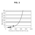
- FIG. 3 is a graph for showing a relationship between a thickness of a silicon nitride film and a time for erasing data in an ultraviolet-erasable nonvolatile semiconductor storage element.
- the ultraviolet-erasable nonvolatile semiconductor device includes a semiconductor substrate 10, a nonvolatile semiconductor storage element 17 formed in the semiconductor substrate 10, a top metal 11 formed on the semiconductor substrate 10, and a protective film formed on the top metal 11. Further, the ultraviolet-erasable nonvolatile semiconductor device includes, in part thereof, a pad opening portion 14 obtained by removing the protective film formed on the top metal 11.
- the protective film includes two layers of a silicon nitride film 12 and a silicon oxynitride film 13.
- the silicon nitride film 12 and the silicon oxynitride film 13 cooperate to prevent moisture from penetrating into the ultraviolet-erasable nonvolatile semiconductor device.
- a thickness of the silicon nitride film 12 is increased, ultraviolet rays are more difficult to transmit therethrough, and hence such a thickness is selected with which it is possible to shorten the time for erasing data in the nonvolatile semiconductor storage element 17 through irradiation of the ultraviolet rays.
- the nonvolatile semiconductor storage element 17 such as an erasable programmable read only memory (EPROM) is formed in the semiconductor substrate 10. After that, an inter-layer insulating film (not shown) and the like are laminated on the resultant, and then the top metal 11 is laminated thereon. After that, as the protective film, the silicon nitride film 12 and then the silicon oxynitride film 13 are laminated thereon. After that, the pad opening portion 14 is formed in part of the protective film formed on the top metal 11.
- EPROM erasable programmable read only memory
- the silicon nitride film 12 is formed so as to have a thickness of about 1,000 ⁇ or more in orderto ensure the water resistance. Moreover, as shown in FIG. 3 , when the thickness of the silicon nitride film 12 exceeds about 2,000 ⁇ , the time for erasing data in the ultraviolet-erasable nonvolatile semiconductor storage element is precipitously increased. Thus, it is required that the thickness of the silicon nitride film 12 be set to be about 2,000 ⁇ or less so that the time for erasing data is not unnecessarily increased. With this, the data in the nonvolatile semiconductor storage element 17 can be erased by the ultraviolet rays even in the manufacturing process.
- the silicon oxynitride film 13 is formed so as to have a refractive index of from 1.65 to 1.85 and a thickness of about 7,000 ⁇ or more, and hence the water resistance can be enhanced. Note that, the silicon oxynitride film 13 does not inhibit the entrance of the ultraviolet rays.
- the ultraviolet-erasable nonvolatile semiconductor device can have the high water resistance and erase the data by the ultraviolet rays within a period of time that allows the mass production.
- the silicon oxynitride film 13 is laminated on the silicon nitride film 12.
- the silicon nitride film 12 may be laminated on the silicon oxynitride film 13.
- a TEOS film 15 may be added as the protective film between the silicon nitride film and the silicon oxynitride film.
Landscapes
- Non-Volatile Memory (AREA)
- Semiconductor Memories (AREA)
- Internal Circuitry In Semiconductor Integrated Circuit Devices (AREA)
- Formation Of Insulating Films (AREA)
Abstract
Description
- The present invention relates to an ultraviolet-erasable nonvolatile semiconductor device.
- Erosion by moisture has been a concern in a semiconductor device represented by a semiconductor integrated circuit. In order to cope with this, as disclosed in Patent Literature 1, a nitride film having an excellent water resistance is formed on a surface of the semiconductor device so that moisture is prevented from penetrating into the semiconductor device, to thereby enhance a water resistance of the semiconductor device.
- [PTL 1]
JP 2006-344956 A - However, when the technology disclosed in Patent Literature 1 is applied to an ultraviolet-erasable nonvolatile semiconductor device capable of erasing data by ultraviolet rays, due to the presence of the nitride film, the water resistance of the semiconductor device is enhanced but the ultraviolet rays are difficult to transmit therethrough, and hence the data cannot be erased by the ultraviolet rays or a large amount of time is required to erase the data. Thus, a structure has been demand that has a high water resistance and is suitable for an ultraviolet-erasable nonvolatile semiconductor device capable of erasing data by ultraviolet rays.
- The present invention has been made in view of the problems described above, and provides an ultraviolet-erasable nonvolatile semiconductor device that has a high water resistance and is capable of erasing data by ultraviolet rays.
- In order to solve the problems described above, according to one embodiment of the present invention, there is provided an ultraviolet-erasable nonvolatile semiconductor device, including: a semiconductor substrate; a nonvolatile semiconductor storage element formed in the semiconductor substrate; a top metal formed on the semiconductor substrate; and a protective film formed on the top metal. The protective film includes a silicon nitride film and a silicon oxynitride film. The silicon nitride film and the silicon oxynitride film cooperate to prevent moisture from penetrating into the ultraviolet-erasable nonvolatile semiconductor device. The silicon nitride film has such a thickness with which it is possible to shorten a time for erasing data in the nonvolatile semiconductor storage element through irradiation of ultraviolet rays.
- The ultraviolet-erasable nonvolatile semiconductor device according to the one embodiment of the present invention has the high water resistance and is capable of erasing the data by the ultraviolet rays.
-
-
FIG. 1 is a sectional view of an ultraviolet-erasable nonvolatile semiconductor device. -
FIG. 2 is a sectional view of an ultraviolet-erasable nonvolatile semiconductor device. -
FIG. 3 is a graph for showing a relationship between a thickness of a silicon nitride film and a time for erasing data in an ultraviolet-erasable nonvolatile semiconductor storage element. - In the following, embodiments of the present invention are described with reference to the drawings.
- An ultraviolet-erasable nonvolatile semiconductor device is now described.
FIG. 1 is a sectional view of the ultraviolet-erasable nonvolatile semiconductor device.FIG. 3 is a graph for showing a relationship between a thickness of a silicon nitride film and a time for erasing data in an ultraviolet-erasable nonvolatile semiconductor storage element. - The ultraviolet-erasable nonvolatile semiconductor device includes a
semiconductor substrate 10, a nonvolatilesemiconductor storage element 17 formed in thesemiconductor substrate 10, atop metal 11 formed on thesemiconductor substrate 10, and a protective film formed on thetop metal 11. Further, the ultraviolet-erasable nonvolatile semiconductor device includes, in part thereof, apad opening portion 14 obtained by removing the protective film formed on thetop metal 11. In this case, the protective film includes two layers of asilicon nitride film 12 and asilicon oxynitride film 13. - Part of the
top metal 11 is exposed from thepad opening portion 14, and necessary signal transmission is performed therewith. Thesilicon nitride film 12 and thesilicon oxynitride film 13 cooperate to prevent moisture from penetrating into the ultraviolet-erasable nonvolatile semiconductor device. As a thickness of thesilicon nitride film 12 is increased, ultraviolet rays are more difficult to transmit therethrough, and hence such a thickness is selected with which it is possible to shorten the time for erasing data in the nonvolatilesemiconductor storage element 17 through irradiation of the ultraviolet rays. - Through a publicly-known semiconductor manufacturing process, the nonvolatile
semiconductor storage element 17 such as an erasable programmable read only memory (EPROM) is formed in thesemiconductor substrate 10. After that, an inter-layer insulating film (not shown) and the like are laminated on the resultant, and then thetop metal 11 is laminated thereon. After that, as the protective film, thesilicon nitride film 12 and then thesilicon oxynitride film 13 are laminated thereon. After that, thepad opening portion 14 is formed in part of the protective film formed on thetop metal 11. - In this case, the
silicon nitride film 12 is formed so as to have a thickness of about 1,000 Å or more in orderto ensure the water resistance. Moreover, as shown inFIG. 3 , when the thickness of thesilicon nitride film 12 exceeds about 2,000 Å, the time for erasing data in the ultraviolet-erasable nonvolatile semiconductor storage element is precipitously increased. Thus, it is required that the thickness of thesilicon nitride film 12 be set to be about 2,000 Å or less so that the time for erasing data is not unnecessarily increased. With this, the data in the nonvolatilesemiconductor storage element 17 can be erased by the ultraviolet rays even in the manufacturing process. - Moreover, the
silicon oxynitride film 13 is formed so as to have a refractive index of from 1.65 to 1.85 and a thickness of about 7,000 Å or more, and hence the water resistance can be enhanced. Note that, thesilicon oxynitride film 13 does not inhibit the entrance of the ultraviolet rays. - With the configuration described above, the ultraviolet-erasable nonvolatile semiconductor device can have the high water resistance and erase the data by the ultraviolet rays within a period of time that allows the mass production.
- Note that, in
FIG. 1 , thesilicon oxynitride film 13 is laminated on thesilicon nitride film 12. Although not illustrated, thesilicon nitride film 12 may be laminated on thesilicon oxynitride film 13. - Moreover, as illustrated in
FIG. 2 , a TEOSfilm 15 may be added as the protective film between the silicon nitride film and the silicon oxynitride film. -
- 10
- semiconductor substrate
- 11
- top metal
- 12
- silicon nitride film
- 13
- silicon oxynitride film
- 14
- pad opening portion
- 15
- TEOS film
- 17
- nonvolatile semiconductor storage element
Claims (4)
- An ultraviolet-erasable nonvolatile semiconductor device, comprising:a semiconductor substrate;an ultraviolet-erasable nonvolatile semiconductor storage element formed in a surface of the semiconductor substrate;a top metal formed on the semiconductor substrate; anda protective film formed on the ultraviolet-erasable nonvolatile semiconductor storage element and the top metal, the protective film comprising a silicon nitride film and a silicon oxynitride film laminated thereon.
- An ultraviolet-erasable nonvolatile semiconductor device according to claim 1, wherein the silicon nitride film has a thickness of 1,000 Å or more and 2,000 Å or less.
- An ultraviolet-erasable nonvolatile semiconductor device according to claim 1, wherein the silicon oxynitride film has a refractive index of from 1.65 to 1.85.
- An ultraviolet-erasable nonvolatile semiconductor device according to claim 1, further comprising a TEOS film formed between the silicon nitride film and the silicon oxynitride film.
Applications Claiming Priority (2)
| Application Number | Priority Date | Filing Date | Title |
|---|---|---|---|
| JP2013032114A JP2014165191A (en) | 2013-02-21 | 2013-02-21 | Ultraviolet ray erasure type nonvolatile semiconductor device |
| PCT/JP2014/051182 WO2014129252A1 (en) | 2013-02-21 | 2014-01-22 | Ultraviolet-erasable nonvolatile semiconductor device |
Publications (2)
| Publication Number | Publication Date |
|---|---|
| EP2960928A1 true EP2960928A1 (en) | 2015-12-30 |
| EP2960928A4 EP2960928A4 (en) | 2016-11-02 |
Family
ID=51391049
Family Applications (1)
| Application Number | Title | Priority Date | Filing Date |
|---|---|---|---|
| EP14754296.3A Withdrawn EP2960928A4 (en) | 2013-02-21 | 2014-01-22 | NON-VOLATILE SEMICONDUCTOR DEVICE DISABLED BY ULTRAVIOLET |
Country Status (7)
| Country | Link |
|---|---|
| US (1) | US9589972B2 (en) |
| EP (1) | EP2960928A4 (en) |
| JP (1) | JP2014165191A (en) |
| KR (1) | KR20150120370A (en) |
| CN (1) | CN105074887A (en) |
| TW (1) | TW201448217A (en) |
| WO (1) | WO2014129252A1 (en) |
Cited By (1)
| Publication number | Priority date | Publication date | Assignee | Title |
|---|---|---|---|---|
| CN106206737A (en) * | 2016-08-19 | 2016-12-07 | 上海华力微电子有限公司 | Half floating transistor process |
Families Citing this family (5)
| Publication number | Priority date | Publication date | Assignee | Title |
|---|---|---|---|---|
| US10230948B2 (en) * | 2016-02-03 | 2019-03-12 | Mediatek Inc. | Video transmitting system with on-the-fly encoding and on-the-fly delivering and associated video receiving system |
| CN107123600A (en) * | 2017-05-19 | 2017-09-01 | 武汉新芯集成电路制造有限公司 | It is a kind of to improve the lithographic method of wafer surface defects |
| CN113809085A (en) * | 2020-06-17 | 2021-12-17 | 和舰芯片制造(苏州)股份有限公司 | Flash memory and preparation method thereof |
| CN112802855B (en) * | 2021-03-27 | 2023-06-02 | 长江存储科技有限责任公司 | Three-dimensional memory device, manufacturing method thereof, and three-dimensional memory |
| US20240102830A1 (en) * | 2022-09-27 | 2024-03-28 | Texas Instruments Incorporated | Barrier layers for anisotropic magneto-resistive sensors |
Family Cites Families (9)
| Publication number | Priority date | Publication date | Assignee | Title |
|---|---|---|---|---|
| JPS61140155A (en) * | 1984-12-12 | 1986-06-27 | Hitachi Ltd | Semiconductor device |
| JPS6428869A (en) * | 1987-07-23 | 1989-01-31 | Mitsubishi Electric Corp | Semiconductor device |
| JPH05299661A (en) * | 1992-04-17 | 1993-11-12 | Sony Corp | Nonvolatile semiconductor device |
| JPH05299660A (en) * | 1992-04-21 | 1993-11-12 | Nippondenso Co Ltd | Manufacture of semiconductor device |
| EP0738424B1 (en) * | 1994-11-07 | 2010-05-19 | Macronix International Co., Ltd. | Integrated circuit passivation process |
| US20030082905A1 (en) * | 2001-10-31 | 2003-05-01 | Jen-Ku Hung | Method for forming a uniform damascene profile |
| KR100703971B1 (en) * | 2005-06-08 | 2007-04-06 | 삼성전자주식회사 | Semiconductor integrated circuit device and manufacturing method thereof |
| US7828987B2 (en) * | 2006-03-20 | 2010-11-09 | Applied Materials, Inc. | Organic BARC etch process capable of use in the formation of low K dual damascene integrated circuits |
| KR100832715B1 (en) * | 2006-12-23 | 2008-05-28 | 동부일렉트로닉스 주식회사 | Manufacturing Method of Flash Memory Device |
-
2013
- 2013-02-21 JP JP2013032114A patent/JP2014165191A/en active Pending
-
2014
- 2014-01-22 EP EP14754296.3A patent/EP2960928A4/en not_active Withdrawn
- 2014-01-22 KR KR1020157022415A patent/KR20150120370A/en not_active Withdrawn
- 2014-01-22 US US14/769,048 patent/US9589972B2/en not_active Expired - Fee Related
- 2014-01-22 WO PCT/JP2014/051182 patent/WO2014129252A1/en not_active Ceased
- 2014-01-22 CN CN201480009981.4A patent/CN105074887A/en active Pending
- 2014-02-06 TW TW103103927A patent/TW201448217A/en unknown
Cited By (1)
| Publication number | Priority date | Publication date | Assignee | Title |
|---|---|---|---|---|
| CN106206737A (en) * | 2016-08-19 | 2016-12-07 | 上海华力微电子有限公司 | Half floating transistor process |
Also Published As
| Publication number | Publication date |
|---|---|
| JP2014165191A (en) | 2014-09-08 |
| EP2960928A4 (en) | 2016-11-02 |
| KR20150120370A (en) | 2015-10-27 |
| WO2014129252A1 (en) | 2014-08-28 |
| US9589972B2 (en) | 2017-03-07 |
| CN105074887A (en) | 2015-11-18 |
| US20160005744A1 (en) | 2016-01-07 |
| TW201448217A (en) | 2014-12-16 |
Similar Documents
| Publication | Publication Date | Title |
|---|---|---|
| US9589972B2 (en) | Ultraviolet-erasable nonvolatile semiconductor device | |
| CN109075166B (en) | Integrated structure and method for forming the same | |
| JP2017195367A5 (en) | Flexible device fabrication method | |
| US7544992B2 (en) | Illuminating efficiency-increasable and light-erasable embedded memory structure | |
| US20160365539A1 (en) | Organic light emitting display device and method for packaging organic light emitting diode | |
| US9465242B1 (en) | Display panel and display device | |
| WO2014031341A3 (en) | Structures and methods of making nand flash memory | |
| TW201712879A (en) | Semi-volatile embedded memory with between-fin floating-gate device and method | |
| CN105845681B (en) | Non-volatile memory and method of making the same | |
| TW200727415A (en) | Methods for fabricating semiconductor chip, semiconductor device and non-volatile memory device | |
| CN105470202A (en) | Manufacture method for tip of floating gate of split-gate flash memory | |
| BR112014019132A8 (en) | SIGNAL PROCESSING DEVICE | |
| WO2008155832A1 (en) | Semiconductor device, and its manufacturing method | |
| US20200144275A1 (en) | Flash memories and methods for manufacturing the same | |
| TW200640010A (en) | Multi-layered thin films, thin film transistor array panel nicluding the same, and method of manufacturing the panel | |
| TW200802818A (en) | Nonvolatile memory device and method of fabricating the same | |
| EP3327752B1 (en) | A semiconductor device and manufacturing method thereof | |
| TW200719482A (en) | Flash memory device and method of manufacturing the same | |
| TWM564824U (en) | Display widget | |
| CN101777518A (en) | Method for improving integral parameter of gate oxide layer | |
| TW200507278A (en) | Transistor manufacturing method, electro-optic device and electronic instrument | |
| KR102146044B1 (en) | Semiconductor device | |
| CN103531532A (en) | Method for forming contact window | |
| WO2009057212A1 (en) | Semiconductor device and its manufacturing method | |
| US20130181276A1 (en) | Non-self aligned non-volatile memory structure |
Legal Events
| Date | Code | Title | Description |
|---|---|---|---|
| PUAI | Public reference made under article 153(3) epc to a published international application that has entered the european phase |
Free format text: ORIGINAL CODE: 0009012 |
|
| 17P | Request for examination filed |
Effective date: 20150921 |
|
| AK | Designated contracting states |
Kind code of ref document: A1 Designated state(s): AL AT BE BG CH CY CZ DE DK EE ES FI FR GB GR HR HU IE IS IT LI LT LU LV MC MK MT NL NO PL PT RO RS SE SI SK SM TR |
|
| AX | Request for extension of the european patent |
Extension state: BA ME |
|
| RAP1 | Party data changed (applicant data changed or rights of an application transferred) |
Owner name: SII SEMICONDUCTOR CORPORATION |
|
| DAX | Request for extension of the european patent (deleted) | ||
| A4 | Supplementary search report drawn up and despatched |
Effective date: 20160930 |
|
| RIC1 | Information provided on ipc code assigned before grant |
Ipc: H01L 23/31 20060101ALI20160926BHEP Ipc: H01L 21/336 20060101AFI20160926BHEP Ipc: H01L 27/115 20060101ALI20160926BHEP Ipc: H01L 21/8247 20060101ALI20160926BHEP Ipc: H01L 21/3205 20060101ALI20160926BHEP Ipc: H01L 21/768 20060101ALI20160926BHEP Ipc: H01L 23/522 20060101ALI20160926BHEP Ipc: H01L 23/532 20060101ALI20160926BHEP Ipc: H01L 29/788 20060101ALI20160926BHEP Ipc: H01L 29/792 20060101ALI20160926BHEP |
|
| STAA | Information on the status of an ep patent application or granted ep patent |
Free format text: STATUS: THE APPLICATION IS DEEMED TO BE WITHDRAWN |
|
| 18D | Application deemed to be withdrawn |
Effective date: 20170429 |