EP2955152B1 - Unite de stockage d'informations, support d'informations optique, dispositif de stockage d'informations dans une unite de stockage d'informations, utilisation d'une unite de stockage d'informations en tant qu'affichage passif et agencement de capteur - Google Patents
Unite de stockage d'informations, support d'informations optique, dispositif de stockage d'informations dans une unite de stockage d'informations, utilisation d'une unite de stockage d'informations en tant qu'affichage passif et agencement de capteur Download PDFInfo
- Publication number
- EP2955152B1 EP2955152B1 EP15176791.0A EP15176791A EP2955152B1 EP 2955152 B1 EP2955152 B1 EP 2955152B1 EP 15176791 A EP15176791 A EP 15176791A EP 2955152 B1 EP2955152 B1 EP 2955152B1
- Authority
- EP
- European Patent Office
- Prior art keywords
- nanoparticles
- charge carriers
- arrangement
- information storage
- electric field
- Prior art date
- Legal status (The legal status is an assumption and is not a legal conclusion. Google has not performed a legal analysis and makes no representation as to the accuracy of the status listed.)
- Active
Links
Images


Classifications
-
- B—PERFORMING OPERATIONS; TRANSPORTING
- B82—NANOTECHNOLOGY
- B82Y—SPECIFIC USES OR APPLICATIONS OF NANOSTRUCTURES; MEASUREMENT OR ANALYSIS OF NANOSTRUCTURES; MANUFACTURE OR TREATMENT OF NANOSTRUCTURES
- B82Y20/00—Nanooptics, e.g. quantum optics or photonic crystals
-
- G—PHYSICS
- G09—EDUCATION; CRYPTOGRAPHY; DISPLAY; ADVERTISING; SEALS
- G09F—DISPLAYING; ADVERTISING; SIGNS; LABELS OR NAME-PLATES; SEALS
- G09F13/00—Illuminated signs; Luminous advertising
- G09F13/20—Illuminated signs; Luminous advertising with luminescent surfaces or parts
- G09F13/22—Illuminated signs; Luminous advertising with luminescent surfaces or parts electroluminescent
Definitions
- the present invention relates to information stores, to optical information carriers, to a use of an information store for a passive display, to a device for storing information in an information store and to a method for storing information.
- the present invention relates to the storage of information in a nanoparticle arrangement by electrical means and to reading out the stored information by optical means at a later point in time.
- the present invention further relates to a sensor arrangement using the information memory, to a mechanical component with an integrated sensor arrangement for monitoring and displaying a mechanical load acting on the mechanical component, to a method for displaying and storing a mechanical load applied to a mechanical component, and to the use of a semiconductor nanocrystal arrangement for the visualization (storage and / or display) of a mechanical load that is detected by a force-sensitive element and acting on a mechanical component.
- the present invention relates to methods and devices for detecting, storing and evaluating static or dynamic loads on mechanical components using a force-sensitive element and a display element connected to the force-sensitive element, the display element having a semiconductor nanocrystal arrangement for providing a fluorescence property which can be changed or adjusted based on an amount of electrical charge that is supplied to the semiconductor nanocrystal arrangement by the force-sensitive element.
- Quantum dot displays As a special group of displays, reference is made at this point to so-called quantum dot displays, which use the effect of electroluminescence.
- Quantum dot displays contain nanoparticles, which typically refer to a composite of several thousand atoms or molecules. The nanoparticles often have a regular structure, such as a crystal structure.
- electrically generated holes and electrons are directed to the nanoparticles in a suitable manner, in which the charge carriers recombine immediately with the emission of light.
- Quantum dot displays are dealt with in the following patent applications, for example: WO 2009/058172 A1 ("Device containing nonblinking Quantum Dots”), US 2009/0091689 A1 (“Display Device”), US 2006/0170331 A1 ("Electroluminescent Device with Quantum Dots”), US 2010/0109521 A1 ("Quantum Dot Electroluminescent Device "), WO 2008/112062 A2 ("Quantum Dot Light Emitting Device”) and US 2008/0309234 A1 ("Alternating Current Driving Type Quantum Dot Electroluminescent Device”).
- devices that can be classified between the first group and the second group there are also devices that can be classified between the first group and the second group.
- These are, for example, school boards or whiteboards. With blackboards, the information is fixed by applying chalk to a slate or plastic surface until the chalk is washed off or wiped off.
- Whiteboards are based on a similar principle, but instead of chalk, an ink is used that adheres to the surface of the whiteboard. To erase the information, the whiteboard is wiped with a cloth to which the ink sticks better than to the whiteboard.
- School blackboards and whiteboards combine energy-free storage of information with frequent rewriting. Due to their functional principle, however, the use of blackboards and whiteboards is accompanied by a build-up of dust and a risk of contamination.
- Stored information can also be used as an indicator for the state of e.g. a mechanical component.
- Alloys, ceramic materials, plastics and composite materials are used to an increasing extent in many technical fields using mechanical systems, such as for example in aircraft construction, vehicle construction, mechanical engineering and other fields, for weight reduction and for improving system properties.
- damage to the material for example caused by mechanical overload, is not immediately visible and can therefore remain undetected.
- this material damage can lead to sudden, unforeseen breakage or failure of the mechanical component, which can result in the failure of entire assemblies or the entire system.
- Mechanical components are designed for a specific load spectrum for optimal use of the resources used and for cost optimization in the respective design.
- the limits of mechanical strength and reliability for example determined in advance in extensive tests.
- safety-relevant components for example in vehicles (trains, buses, etc.), ships or aircraft, are regularly checked for their condition during operation as part of a maintenance plan.
- x-ray examinations, ultrasound measurements or microscopic examinations using electron or ion beam methods are used for this purpose.
- a decisive disadvantage of these procedures is that they cannot be used "in-situ" (in a natural position), ie continuously on site, but are generally only used within the framework of fixed maintenance cycles.
- the U.S. 6,720,589 relates to semiconductor components that can be configured as optically activated memories or single photon detectors.
- the components include an active layer with a plurality of quantum dots and an active layer.
- the components are configured so that the charge stored in the quantum dots influences the transport and / or the optical characteristics of the active layer.
- an information memory according to claim 1 an optical information carrier according to claim 7, a use of an information memory according to claim 9, a device for storing information according to claim 10 and a method for storing information according to claim 13.
- a core idea of the present invention is to use a nanoparticle arrangement within an information memory, wherein the information to be stored can be stored in the nanoparticle arrangement by means of an electrical effect and can be read out by means of an optical effect.
- the nanoparticle arrangement comprises a multiplicity of nanoparticles and a support material surrounding the nanoparticles.
- the support material can e.g. be a liquid, a solid material or a gel-like material.
- the nanoparticles are distributed in the support material, it being possible for either a homogeneous distribution or a heterogeneous local distribution to be present.
- a quantum dot is a nanoscopic material structure which, in embodiments of the disclosed technical teaching, has a semiconductor material in the form of semiconductor nanoparticles.
- the charge carriers (electrons or holes) in a quantum dot are so limited in their mobility in all three spatial directions that their energy can no longer assume continuous values, but only discrete values.
- the atomic order of magnitude of quantum dots is about 10 2 to 10 5 atoms.
- semiconductor nanoparticles based on the size of the semiconductor nanoparticles to set and generate a very large bandwidth in the emission spectrum of the nanoparticle arrangement.
- suitable semiconductor materials for nanoparticles can be used which, depending on the size and material, are in a wavelength range, e.g. emit light from 400 nm to 1700 nm, with the spectral range visible to humans extending from about 380 nm to 780 nm.
- nanoparticles of both the core type and the core / shell type of the semiconductor materials CdSe, CdTe, GaAs, HgTe, InAs, InP, InSb, PbSe, PbS, PbTe, ZnSe, ZnTe, germanium and silicon.
- the electrical charge carriers are fed to the nanoparticles in a selective manner in certain areas.
- nanoparticles that are located in a selected area of the nanoparticle arrangement can receive a relatively high average amount of charge carriers, whereas those located outside the selected area Nanoparticles receive a lower average amount of charge carriers.
- the information memory is designed to selectively supply electrical charge carriers to at least some nanoparticles within a local subset of the nanoparticles in the first operating state and to charge these nanoparticles electrically.
- selectivity can be achieved, for example, by appropriate spatial shaping of the electric field. If the electric field spreads essentially locally, the selected area can be defined relatively exactly.
- electrodes with which the electric field is generated can have the shape of a plate capacitor in which the electric field lines run essentially parallel.
- the field generated between the plates of the plate capacitor is significantly stronger than the field generated outside the plates, so that the electric field is essentially only strong enough between the plates to cause the charge carriers to be fed to the nanoparticles.
- the boundary between the selected area and the unselected area can have a transition area in which the charge carrier quantities contained in the nanoparticles gradually decrease or increase.
- the selected area can comprise several sub-areas, which can optionally also be disjoint from one another. Furthermore, the selected area can also cover the entire storage element or the entire nanoparticle arrangement.
- the charge carriers supplied are largely prevented from flowing out of the nanoparticles.
- a significant proportion of the charge carriers previously supplied to the nanoparticles (during the first operating state) are permanently held in the nanoparticles, so that an amount of charge carriers present after a period of time is within a tolerance range of an originally supplied amount of charge carriers.
- the second operating state can last a relatively long time and the nanoparticle arrangement typically does not require any externally supplied energy in order to maintain the second operating state.
- the nanoparticle arrangement can prevent the outflow of the charge carriers to such an extent that the stored information can still be reliably read out, periods of a few minutes, hours, days, weeks, months or even years are possible.
- the discharge of charge carriers from the nanoparticles is typically a statistical effect that is somewhat similar to the decay of radioactive elements. Accordingly, for a specific nanoparticle arrangement, for example, a half-life or another useful variable can be specified.
- the storage element can be reliably read as long as at least 90% of the originally supplied charge carriers are still present in the nanoparticle arrangement, which can be used as a measure of the average storage time that can be achieved.
- a change in the fluorescence properties of the nanoparticles as a result of the charge carriers supplied can consist, for example, in the fact that a radiative recombination, which normally can be observed, is suppressed in the event of optical excitation.
- areas in which charge carriers have been added to the nanoparticles can be recognized by the fact that they light up comparatively darker or not light up at all when they are optically stimulated.
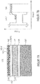
- FIG. 1A shows a schematic diagram of an information memory in a simple form that functions according to the mechanism of action.
- the information memory comprises an electrode 1, a charge carrier-conducting layer 2, and a nanoparticle layer 3.
- the electrode 1 provides charge carriers (electrons or holes).
- the charge carriers are guided by means of the charge carrier-conducting layer 2 to nanoparticles that are contained in the nanoparticle layer 3.
- the charge carrier-conducting layer can be a predominantly hole-conducting material or a predominantly electron-conducting material.
- the charge carriers remain in the nanoparticles if it is the energetically most favorable state for the nanoparticles.
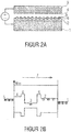
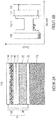
- Figure 3A shows a complementary principle diagram compared to that in Figure 2A illustrated principle diagram.
- Holes serve as charge carriers to be stored in the nanoparticles.
- the voltage is polarized in such a way that the holes are saved and the photoluminescence is suppressed.
- the matrix materials 2, 4 are to be selected so that the transport of holes to the nanoparticles is ensured by the matrix material 2, 4, but the complementary electrons are kept away from the nanoparticles by the matrix material 2, 4.
- the technical teaching presented here enables signs, displays, etc. with which information can be permanently stored with the help of a one-time write process and displayed if the appropriate suggestion. Permanent electrical energy is no longer required for the rest of the process.
- the stored information can be made visible by a simple external optical excitation with a higher-energy UV lamp.
- one or more additional writes may be performed which can be used to add more information to the information already stored.
- the information already stored and the additional information then form a total information item.
- the further writing process can be carried out at a different point in time than the first writing process.
- the two write processes can be separated in time, e.g. a few hours, days, weeks, months, or even years.
- a second, region-wise selective electrical field is generated, with which the further information can be stored in the nanoparticle arrangement. This further writability can be used, for example, to record the state and / or the history of an object or stored information and to reproduce it if necessary.
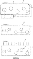
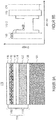
- FIG. 5 Figure 3 is a schematic, perspective view of an information store in accordance with the disclosed teachings.
- the information memory essentially comprises the storage element, which in turn essentially comprises the nanoparticle arrangement 50.
- the nanoparticle arrangement 50 is shown, which comprises the support material 2 and the nanoparticles 3.
- An area is shown on a surface of the nanoparticle arrangement 50 which corresponds to the information to be stored (here the letter “A” as an example).
- Electrons e - are introduced into the nanoparticle arrangement 50 as charge carriers via the surface of the nanoparticle arrangement 50 within the area "A” and move essentially perpendicular to the surface through the nanoparticle arrangement until they are (at least partially) supplied to the nanoparticles 3 present in this area .
- the nanoparticle arrangement comprises a first layer in which mainly nanoparticles of a first size are present. Furthermore, the nanoparticle arrangement comprises a second layer in which nanoparticles of a second size are mainly present, and it comprises a third layer in which nanoparticles of a third size are present.
- the nanoparticles of the first layer are smaller than the nanoparticles of the second layer and the particles of the third layer each have a different size than the nanoparticles of the first and second layer.
- reading out the memory element of the information memory does not represent a "reset” process with regard to the charge carriers stored in the semiconductor nanoparticle arrangement, since the charge carriers are also (at least largely) in the semiconductor nanoparticle arrangement after the memory element has been read out remain saved.
- the information memory can be reset, for example, by applying a correspondingly aligned and sufficiently strong electric field to the semiconductor nanoparticle arrangement in order to "pull out” or remove the charge carriers stored in the semiconductor nanoparticles from the semiconductor nanoparticle arrangement.
- the sensor arrangement 110 is now attached, for example, directly to a mechanical component 160 to be monitored, ie the sensor arrangement 110 can be laminated (in the case of composite materials) for example in the form of a film on or in the mechanical component 160 or, in the case of injection molded parts, can be laminated into the mechanical component during an injection molding process 160 embedded. This enables a force-fit, form-fit or material connection of the force-sensitive element 120 with the mechanical component 160 to be monitored.
- Piezo elements in the form of piezoelectric ceramic materials, polymer films or ceramic-polymer composites, for example, can be used as force-sensitive element 120, with at least one contactable electrode 124 being applied to a piezo layer 122 of force-sensitive element 120 in order to measure the mechanical load there based on a mechanical load Component 160, ie due to an external force, to provide an electrical charge Q 0 of a charge carrier type.
- a further contactable electrode 126 can also be provided, at which a corresponding amount of charge of the charge carrier type complementary (to the electrode 124) can be tapped. If the two electrodes 124, 126 are provided on the force-sensitive element 120, charge quantities Qo of a complementary charge carrier type are provided there.
- the base area of the force-sensitive element 120 of the sensor arrangement 110 can thus be selected as a function of the geometry of the mechanical component 160. Possible thicknesses, for example of a piezo element as the force-sensitive element 120, can range from molecular monolayers up to a few centimeters.
- any sensor elements falling under the generic term “piezo elements” which, based on an acting mechanical load, provide a tapped voltage or amount of charge as an output signal can be used as force-sensitive elements 120.
- the force-sensitive element 120 is now connected (non-positively, positively or cohesively) to the mechanical component 160 to be monitored in order to avoid the mechanical loads and forces acting on the mechanical component 160, which, for example, as deformations of the mechanical component 160 and thus the force-sensitive element 120 occur to be recorded directly at the point of origin on the mechanical component 160.
- the force-sensitive element 120 is thus designed as a so-called force transducer or force sensor, with which a force is measured which acts on the force-sensitive element 120, these being both pressure, tensile, impact and bending loads.
- the mechanical load (s) can be static as well as dynamic.
- the force-sensitive element 120 which z. B. in the form of a piezo layer, an electrical voltage across the force-sensitive element 120 is generated, which can be tapped off as a defined electrical charge quantity Q 0 (a charge carrier polarity) at the contact area 124.
- Q 0 a charge carrier polarity
- the force-sensitive element 120 can thus be designed to provide the electrical charge quantity Q 0 based on the acting mechanical load only when a limit value for the mechanical load is exceeded.
- the force-sensitive element 120 can be designed to continuously increase the amount of electrical charge Q 0 based on and e.g. B. to provide proportional to the acting mechanical load.
- the amount of charge Q 0 provided by the force-sensitive element 120 can on the one hand indicate that a limit value for the mechanical load-bearing capacity of the mechanical component has already been exceeded.
- the amount of charge Q 0 provided by the force-sensitive element 120 can be continuous and e.g. B. generated proportionally to the acting mechanical load, for example, to reproduce the total mechanical load exerted on the mechanical component over a predetermined period of time.
- the force-sensitive element 120 for providing an amount of electrical charge Qo which is based on the mechanical load acting on the coupled mechanical component 160, is now assigned a display element 140 with a semiconductor nanocrystal arrangement 142, the semiconductor nanocrystal arrangement 142 having a fluorescence property that can be set or changed based on an amount of electrical charge (polarity) supplied to the semiconductor nanocrystal arrangement.
- the force-sensitive element 120 is now coupled to the display element 140, that is to say, for example, with a flat or structured electrode 144 of the display element 140, in order to supply at least part of the amount of charge Q 0 generated by the force-sensitive element 120 to the semiconductor nanocrystal arrangement of the display element 140, in order to thereby set or change the fluorescence property of the semiconductor nanocrystal arrangement 142 of the display element 140 based on the mechanical load of the mechanical component 160 to be monitored that is detected by the force-sensitive element 120.
- the display element 140 thus serves as a storage or indicator layer for the loading state of the mechanical component 160.
- the semiconductor nanocrystal arrangement 140 has a large number of semiconductor nanocrystals or semiconductor nanoparticles 142-2 within a carrier material 142-1.
- another transparent for the emitted fluorescence radiation can be placed on the semiconductor nanocrystal arrangement 142
- Protective layer or a transparent and conductive counter electrode layer 148 can be arranged.
- the electrode 144 assigned to the semiconductor nanocrystalline arrangement 142 of the display element 140 is now, for example, via one or more contacting intermediate layers 146, which e.g. B. is / are permeable to the charge carrier type to be supplied to the nanoparticles 142-2 and impermeable to the complementary charge carrier type, connected to the contact area 124 of the force-sensitive element 120.
- the display element 140 is applied as a so-called semiconductor-nanocrystal composite layer via the contacting intermediate layer (s) 146 to the force-sensitive element 120 designed as a piezo element 122, whereby the in Fig. 6 Layer stack shown for the sensor arrangement 110 results.
- Other electrical connections e.g. B.
- the contact area 124 and the electrode 144 can also be designed, for example, as a common element.
- the respective base area of the display element 140 of the sensor arrangement 110 i. W.
- the base area of the display element 140 can thus be selected depending on the geometry of the mechanical component 160. Possible thicknesses of the display element 140 can range from molecular monolayers up to a few millimeters.
- semiconductor nanocrystals with a higher energetic optical excitation S UV z. B. by means of an external excitation device 180 in the form of a UV light source or a laser etc. emit fluorescence according to their band gap fluorescence radiation S fluorescence .
- the excitation of the semiconductor nanocrystals 142-2 in the semiconductor nanocrystal arrangement 142 generates so-called electron-hole pairs (excitons) in the nanocrystals, which recombine with the emission of a fluorescence photon.
- the respective wavelength (ie color) of the fluorescence emission of the display element 140 can be changed by varying the particle size of the semiconductor nanoparticles or the semiconductor nanocrystals [3, 4].
- Semiconductor nanocrystals now have the property that the energy of the emitted fluorescence photons, i.e. the energy distance from the ground state to the excited state, not only from the respective semiconductor material the semiconductor nanocrystals, but also depends on the respective particle size of the semiconductor nanocrystals.
- particles 142-2 of different sizes can be produced from the same semiconductor material, which fluoresce in different colors, the color, ie the emission wavelength, being able to be adjusted by the respective nanoparticle size.
- small particles emit at a smaller wavelength, ie with a larger photon energy, while larger particles emit at larger wavelengths, ie with smaller photon energies (see also quantum confinement effect).
- quantum mechanics it can now be explained that due to the spatial limitation of the charge carriers, the distance between the energy levels depends on the spatial dimensions, ie the particle size. Such systems are also referred to as quantum dots.
- semiconductor materials for nanocrystals or nanoparticles can be used which, depending on the size and material, in a wavelength range, for. B. emit light from 400 nm to 1700 nm, the spectral range visible to humans extending from about 380 to 780 nm.
- nanocrystals of both the core type and the core / shell type of the semiconductor materials CdSe, CdTe, CdS, GaAs, GaSb, HgTe, InAs, InP, InSb, PbSe, PbS, PbTe, ZnSe, ZnTe, germanium and silicon.
- a quantum dot is a nanoscopic material structure which, in exemplary embodiments of the present invention, has a semiconductor material in the form of semiconductor nanoparticles.
- the charge carriers (electrons or holes) in a quantum dot are so limited in their mobility in all three spatial directions that their energy can no longer assume continuous values, but only discrete values.
- the atomic order of magnitude of quantum dots is around 10 2 -10 5 atoms.
- the semiconductor nanoparticles 142-2 are all in one Carrier material 142-1 housed or embedded.
- the quantum dots ie the semiconductor nanoparticles 142-2
- the quantum dots can be provided with a shell or shell layer or a wetting layer, this shell or wetting layer of the semiconductor nanoparticles being specifically formed during their production in such a way that the semiconductor nanoparticles of different sizes respond differently to a charge carrier feed from the electrode layer 144, ie the fluorescence properties of semiconductor nanoparticles of different sizes change differently based on the charge carriers introduced by the piezo element 120.
- the electrode 144 of the display element 140 is now metallized in areas, locally varying reductions in fluorescence (corresponding to the structure of the electrode 144) can be caused in the semiconductor nanocrystalline arrangement 142, so that an optical contrast as a measure of the mechanical load on the mechanical component 160 the emitted fluorescent light (for example to adjacent sensor arrangements 110) is directly visible on the mechanical component to be monitored.
- the metallization of the electrode 144 can now be designed, for example, in such a way that it is assigned to a specific type of semiconductor nanoparticles (if several types of semiconductor nanoparticles are provided) in the semiconductor nanocrystal arrangement 142.
- the semiconductor nanoparticles that are assigned to the electrode regions 144 or are arranged adjacent to the same are preferred that absorb charge carriers that change the fluorescence behavior. It can thereby be achieved that on the one hand the semiconductor nanocrystal arrangement 142 is significantly increased due to increased contrasts between a “normal” fluorescence property and a “changed” fluorescence property.
- intermediate stages according to the respectively supplied, z. B. different amount of charge Q 0 are clearly displayed, so that corresponding intermediate stages of the mechanical load acting on the mechanical component 160 can be reproduced.
- the in Figure 7A electrode 124 shown which at the same time the function of in Fig. 6
- the electrode 144 shown takes over, over the entire surface, ie continuously metallized, or also structured, ie metallized in areas.
- these "delocalized” charges stored in the semiconductor nanocrystals 142-2 influence or “switch off” the fluorescence property of the now ionized semiconductor nanocrystals and thus a local reduction in the intensity (ie the brightness) of the emitted fluorescence radiation.
- the original, external force acting on the mechanical component 160 to be monitored can thus be optically detected locally as a reduced fluorescence property of the display element 140.
- the detectability of a change in the fluorescence property of the display element 140 can be further enhanced by structuring the electrode structure 144, for example in a linear grid, so that in accordance with the ionization of the semiconductor nanocrystals in the vicinity of the metallic areas of the electrode 144, the The associated fluorescence property of the semiconductor nanocrystals changes, so that, for example, a line contrast results which is higher the greater the amount of charge Q 0 provided by force-sensitive element 120.
- different types of semiconductor nanoparticles with different sizes and / or material compositions can of course also be combined in the semiconductor nanocrystal arrangement 140.
- the force-sensitive element 120 for example in the form of a piezo element, is in turn attached to the mechanical component 160 with a force fit.
- the piezo layer 120 is polarized in such a way that the upper electrode 126 of which collect the negative charges, while the positive charge carriers (amount of charge Q 0 ) collect at the lower electrode 124.
- the electrons first collect again at the upper electrode 124, while the positive charges collect at the lower electrode 126, which is connected to the electrode layer 144 of the display element 140 connected is.
- the electrode material as in Figure 8B shown, a lower work function compared to the valence band edge of the semiconductor nanocrystals, it is energetically more favorable for the positive charges to occupy corresponding states in the valence band Ev of the semiconductor nanocrystals 142-2, as is in principle in the energy level diagram of Figure 8B is shown.
- the positive charges therefore flow away via diffusion and tunneling processes in the direction of the semiconductor nanocrystals 142-2 and are stored in them.
Landscapes
- Engineering & Computer Science (AREA)
- Chemical & Material Sciences (AREA)
- Nanotechnology (AREA)
- Physics & Mathematics (AREA)
- Theoretical Computer Science (AREA)
- Biophysics (AREA)
- Optics & Photonics (AREA)
- Life Sciences & Earth Sciences (AREA)
- Crystallography & Structural Chemistry (AREA)
- General Physics & Mathematics (AREA)
- Light Receiving Elements (AREA)
- Luminescent Compositions (AREA)
- Semiconductor Memories (AREA)
- Investigating, Analyzing Materials By Fluorescence Or Luminescence (AREA)
- Optical Recording Or Reproduction (AREA)
Claims (15)
- Dispositif de mémoire d'informations, comportant
un élément de mémoire avec un aménagement de nanoparticules (50) qui comporte une pluralité de nanoparticules (3) et un matériau de support (2) entourant les nanoparticules; et
une électrode structurée (1);
caractérisé par le fait que le dispositif de mémoire est conçupour générer, dans un premier état de fonctionnement, un champ électrique sélectif par zone dans l'aménagement de nanoparticules (50) au moyen de l'électrode structurée (1) qui entre en contact avec une zone partielle du matériau de support (2), de sorte que vers les nanoparticules (3) qui sont détectées par le champ électrique sélectif par zone et qui se situent dans un prolongement de la zone partielle pénétrant dans le matériau de support soient alimentés des porteurs de charge de manière sélective avec une probabilité accrue en comparaison avec les nanoparticules (3) en-dehors de ce prolongement de la zone partielle, etpour terminer, dans un deuxième état de fonctionnement, la génération du champ électrique sélectif par zone, où l'aménagement de nanoparticules (50) empêche amplement une évacuation des porteurs de charge alimentés hors des nanoparticules (3) après la fin, et où les porteurs de charge alimentés réduisent une intensité de fluorescence des nanoparticules (3) vers lesquelles les porteurs de charge électrique ont été alimentés de manière sélective par zone pendant la génération du champ électrique, de sorte que par une excitation optique de l'aménagement de nanoparticules (50) puisse être déterminée la zone partielle dans laquelle les porteurs de charges électriques ont été alimentés de manière sélective par zone vers les nanoparticules (3) pendant le premier état de fonctionnement. - Dispositif de mémoire d'informations selon la revendication 1, dans lequel l'évolution de la bande d'énergie à travers l'aménagement de nanoparticules (50) en ce qui concerne les porteurs de charge dans les nanoparticules (3) présente des minimums locaux, de sorte que, dans le deuxième état de fonctionnement, au moins une partie des porteurs de charge alimentés restent dans les nanoparticules (50) tant qu'une quantité d'énergie ajoutée aux porteurs de charge alimentés n'est pas suffisante pour franchir un mur d'énergie entourant le minimum local,
dans lequel les porteurs de charge alimentés présents dans une nanoparticule (3) réduisent une recombinaison rayonnante dans la nanoparticule et modifient de ce fait les propriétés de fluorescence de la nanoparticule, de sorte que la présence de porteurs de charge alimentés dans la nanoparticule (3) peut être constatée par une mesure d'une photoluminescence sur base de la recombinaison rayonnante lors de l'excitation optique de la nanoparticule (3). - Dispositif de mémoire d'informations selon l'une des revendications précédentes, dans lequel l'élément de mémoire est conçu pour adopter, en-dehors du premier état de fonctionnement et du deuxième état de fonctionnement, un troisième état de fonctionnement dans lequel l'élément de mémoire est conçu pour être effacé en appliquant un champ électrique d'effacement ou par irradiation à l'aide d'une lumière UV intense à ondes courtes et une évacuation des porteurs de charge alimentés ainsi provoquée hors des nanoparticules (3).
- Dispositif de mémoire d'informations selon l'une des revendications précédentes, dans lequel le matériau de support (2) comprend un matériau qui est choisi parmi: les diélectriques, tels que PMMA, PS, PC, PVDF, PA, PP, PE, PVC, les thermoplastiques (PET, polyéther cétones), les thermodurcissables (polyesters, résines de formaldéhyde, résines époxy, polyuréthanes); les matériaux conducteurs, tels que poly-électrolytes, PEDOT, BCP, TPD, PPy, complexes TCNQ, PANI, PVK, tétracène, pentacène, phtalocyanines, polythiophènes, PTCDA, MePTCDI, quinacridone, acridone, indanthrone, flavanthrone, périnone, Alq3, P3HT, CNT,
dans lequel le matériau de support (2) comporte le matériau sélectionné sous forme pure, sous forme dopée ou sous forme de dérivé. - Dispositif de mémoire d'informations selon l'une des revendications précédentes, dans lequel l'aménagement de nanoparticules (50) comporte une première, une deuxième et une troisième couche, dans lequel prédominent, dans la première couche, les nanoparticules d'une grosseur dans une première plage de grosseurs, prédominent, dans la deuxième couche, les nanoparticules d'une grosseur dans une deuxième plage de tailles et, dans la troisième couche, les nanoparticules d'une grosseur dans une troisième plage de grosseurs.
- Dispositif de mémoire d'informations selon l'une des revendications précédentes, comportant par ailleurs un aménagement d'électrodes (1, 5) qui est conçu pour générer, dans le premier état de fonctionnement, un champ électrique dans l'aménagement de nanoparticules (50), de sorte que des porteurs de charge soient guidés vers les nanoparticules et qu'au moins une partie de ces derniers restent, comme porteurs de charge alimentés vers les nanoparticules (3) comme les porteurs de charge alimentés.
- Support optique d'informations comportant un dispositif de mémoire d'informations selon l'une des revendications 1 à 6.
- Support optique d'informations selon la revendication 7, comportant par ailleurs une source de lumière destinée à exciter optiquement l'élément de mémoire du dispositif de mémoire d'informations.
- Utilisation d'un dispositif de mémoire d'informations selon l'une des revendications 1 à 6 pour un affichage passif.
- Appareil pour mémoriser les informations dans un dispositif de mémoire d'informations selon l'une des revendications 1 à 6, comportant
un moyen de réception (87) qui est conçu pour recevoir le dispositif de mémoire d'informations (9); et
un aménagement d'électrodes (1, 5) comportant au moins l'électrode structurée (1) qui est conçue pour entrer en contact avec le dispositif de mémoire d'informations (9) lorsque le dispositif de mémoire d'informations est présent dans le moyen de réception (87), et pour générer de manière sélective par zone un champ électrique dans le dispositif de mémoire d'informations (9). - Dispositif selon la revendication 10, dans lequel l'aménagement d'électrodes comporte une électrode d'effacement qui est conçue pour soumettre le dispositif de mémoire d'informations (9) à un champ électrique plus fort que le champ électrique utilisé pour mémoriser les informations, dans lequel l'électrode d'effacement s'étend au moins dans une dimension de sorte qu'un effacement d'un élément de mémoire sensiblement plat puisse avoir lieu en plaçant sur ou en balayant l'élément de mémoire par l'électrode d'effacement, où les porteurs de charge alimentés auparavant vers les nanoparticules sont sensiblement évacués des nanoparticules au moyen d'un puissant champ électrique.
- Dispositif selon l'une des revendications 10 à 11, comportant par ailleurs une source de rayonnement pour effacer le dispositif de mémoire d'informations qui est conçue pour émettre un rayonnement électromagnétique d'une énergie supérieure en direction du dispositif de mémoire d'informations dont l'énergie est suffisante pour évacuer hors des nanoparticules les porteurs de charge alimentés auparavant vers les nanoparticules.
- Procédé de mémorisation d'informations, comportant le fait de:prévoir un aménagement de nanoparticules (50) qui comporte une pluralité de nanoparticules (3) et un matériau de support (2) entourant les nanoparticules;caractérisé par le fait de:générer un champ électrique sélectif par zone dans l'aménagement de nanoparticules (50) au moyen d'une électrode structurée (1) qui entre en contact avec une zone partielle du matériau de support (2), de sorte que vers les nanoparticules (3) qui sont détectées par le champ électrique sélectif par zone et qui se situent dans un prolongement de la zone partielle pénétrant dans le matériau de support, soient alimentés des porteurs de charge de manière sélective avec une probabilité accrue en comparaison avec les nanoparticules (3) en-dehors de ce prolongement de la zone partielle; etterminer la génération du champ électrique sélectif par zone, où l'aménagement de nanoparticules (50) empêche amplement une évacuation des porteurs de charge alimentés hors des nanoparticules (3) après la fin et où les porteurs de charge alimentés réduisent une intensité de fluorescence des nanoparticules (3) vers lesquelles ont été alimentés de manière sélective par zone les porteurs de charge électrique pendant la génération du champ électrique, de sorte que par l'excitation optique de l'aménagement de nanoparticules (50) puisse être déterminée ladite zone partielle dans laquelle les porteurs de charges électriques ont été alimentés de manière sélective par zone vers les nanoparticules (3) pendant le premier état de fonctionnement.
- Procédé selon la revendication 13, comportant par ailleurs le fait de:
générer un champ électrique d'extinction ou un rayonnement électromagnétique d'extinction à énergie supérieure dans l'aménagement de nanoparticules (50) avant la génération du champ sélectif par zone. - Procédé selon l'une des revendications 13 à 14, comportant par ailleurs le fait de:
générer un deuxième champ électrique sélectif par zone dans l'aménagement de nanoparticules (50), de sorte que vers les nanoparticules (3) qui sont détectées par le deuxième champ électrique sélectif par zone soient alimentés des porteurs de charge additionnels, où la génération du champ électrique sélectif par zone et du deuxième champ électrique sélectif par zone ait lieu à des moments différents.
Applications Claiming Priority (4)
| Application Number | Priority Date | Filing Date | Title |
|---|---|---|---|
| DE102010064237 | 2010-12-28 | ||
| DE102011076535A DE102011076535A1 (de) | 2011-05-26 | 2011-05-26 | Informationsspeicher, optischer informationsträger, vorrichtung zum speichern von informationen in informationsspeicher und verwendung eines informationsspeichers als passives display |
| EP11815614.0A EP2658809B1 (fr) | 2010-12-28 | 2011-12-27 | Capteur et méthode d'affichage et de stockage d'une charge mécanique sur un élément. |
| PCT/EP2011/074104 WO2012089739A2 (fr) | 2010-12-28 | 2011-12-27 | Mémoire d'informations, support d'informations optique, dispositif servant à mémoriser des informations dans des mémoires d'informations, utilisation d'une mémoire d'informations en tant que dispositif d'affichage passif et dispositif détecteur |
Related Parent Applications (2)
| Application Number | Title | Priority Date | Filing Date |
|---|---|---|---|
| EP11815614.0A Division-Into EP2658809B1 (fr) | 2010-12-28 | 2011-12-27 | Capteur et méthode d'affichage et de stockage d'une charge mécanique sur un élément. |
| EP11815614.0A Division EP2658809B1 (fr) | 2010-12-28 | 2011-12-27 | Capteur et méthode d'affichage et de stockage d'une charge mécanique sur un élément. |
Publications (2)
| Publication Number | Publication Date |
|---|---|
| EP2955152A1 EP2955152A1 (fr) | 2015-12-16 |
| EP2955152B1 true EP2955152B1 (fr) | 2020-09-30 |
Family
ID=45560876
Family Applications (2)
| Application Number | Title | Priority Date | Filing Date |
|---|---|---|---|
| EP15176791.0A Active EP2955152B1 (fr) | 2010-12-28 | 2011-12-27 | Unite de stockage d'informations, support d'informations optique, dispositif de stockage d'informations dans une unite de stockage d'informations, utilisation d'une unite de stockage d'informations en tant qu'affichage passif et agencement de capteur |
| EP11815614.0A Not-in-force EP2658809B1 (fr) | 2010-12-28 | 2011-12-27 | Capteur et méthode d'affichage et de stockage d'une charge mécanique sur un élément. |
Family Applications After (1)
| Application Number | Title | Priority Date | Filing Date |
|---|---|---|---|
| EP11815614.0A Not-in-force EP2658809B1 (fr) | 2010-12-28 | 2011-12-27 | Capteur et méthode d'affichage et de stockage d'une charge mécanique sur un élément. |
Country Status (2)
| Country | Link |
|---|---|
| EP (2) | EP2955152B1 (fr) |
| WO (1) | WO2012089739A2 (fr) |
Family Cites Families (17)
| Publication number | Priority date | Publication date | Assignee | Title |
|---|---|---|---|---|
| NL262636A (fr) * | 1960-03-23 | 1900-01-01 | ||
| GB2283128B (en) * | 1993-10-21 | 1997-08-20 | Hitachi Europ Ltd | Memory device |
| JP2905739B2 (ja) * | 1996-04-24 | 1999-06-14 | 株式会社エイ・ティ・アール光電波通信研究所 | 全光型半導体画像記憶装置とその画像記憶及び消去方法、及び全光型半導体論理演算装置とその論理演算方法 |
| US6720589B1 (en) * | 1998-09-16 | 2004-04-13 | Kabushiki Kaisha Toshiba | Semiconductor device |
| US7301199B2 (en) * | 2000-08-22 | 2007-11-27 | President And Fellows Of Harvard College | Nanoscale wires and related devices |
| WO2004081141A1 (fr) | 2003-03-11 | 2004-09-23 | Philips Intellectual Property & Standards Gmbh | Diode electroluminescente a points quantiques |
| US20060215958A1 (en) | 2004-11-17 | 2006-09-28 | Yeo Terence E | Enhanced electroluminescent sign |
| GB2439595B (en) * | 2006-06-28 | 2008-11-05 | Toshiba Res Europ Ltd | A quantum memory device |
| GB2440569B (en) * | 2006-07-31 | 2008-07-23 | Toshiba Res Europ Ltd | A photon detector and a method of fabricating a photon detector |
| US8676016B2 (en) * | 2007-02-16 | 2014-03-18 | The Governing Council Of The University Of Toronto | Compressible photonic crystal |
| US7888700B2 (en) | 2007-03-08 | 2011-02-15 | Eastman Kodak Company | Quantum dot light emitting device |
| KR101453082B1 (ko) | 2007-06-15 | 2014-10-28 | 삼성전자주식회사 | 교류 구동형 양자점 전계발광소자 |
| GB2451884A (en) * | 2007-08-16 | 2009-02-18 | Sharp Kk | A Semiconductor Device and a Method of Manufacture Thereof |
| KR101376755B1 (ko) | 2007-10-09 | 2014-03-24 | 삼성디스플레이 주식회사 | 표시장치 |
| US7777233B2 (en) | 2007-10-30 | 2010-08-17 | Eastman Kodak Company | Device containing non-blinking quantum dots |
| GB2460666A (en) * | 2008-06-04 | 2009-12-09 | Sharp Kk | Exciton spin control in AlGaInN quantum dots |
| US20100109521A1 (en) | 2008-10-21 | 2010-05-06 | San Ming Yang | Quantum dot electroluminescent device |
-
2011
- 2011-12-27 EP EP15176791.0A patent/EP2955152B1/fr active Active
- 2011-12-27 EP EP11815614.0A patent/EP2658809B1/fr not_active Not-in-force
- 2011-12-27 WO PCT/EP2011/074104 patent/WO2012089739A2/fr not_active Ceased
Non-Patent Citations (1)
| Title |
|---|
| None * |
Also Published As
| Publication number | Publication date |
|---|---|
| EP2658809B1 (fr) | 2018-05-16 |
| EP2658809A2 (fr) | 2013-11-06 |
| WO2012089739A2 (fr) | 2012-07-05 |
| EP2955152A1 (fr) | 2015-12-16 |
| WO2012089739A3 (fr) | 2012-09-07 |
Similar Documents
| Publication | Publication Date | Title |
|---|---|---|
| Rehman et al. | Resistive switching in all-printed, flexible and hybrid MoS2-PVA nanocomposite based memristive device fabricated by reverse offset | |
| DE69831860T2 (de) | Elektrode zur verwendung in elektrooptischen bauelementen | |
| DE69713500T2 (de) | Schichtiges medium und verfahren zur erzeugung von mustern | |
| DE102014221525B4 (de) | Messsystem | |
| EP2291861A1 (fr) | Photodétecteur et son procédé de production | |
| EP1629270A2 (fr) | Structure composite a semi-conducteur parametree comprenant des canaux de dopage integres, procede pour la produire et son utilisation | |
| DE102011086168A1 (de) | Organisches licht emittierendes bauelement | |
| DE112011101062T5 (de) | Organische elektrolumineszierende Vorrichtung | |
| EP3520098B1 (fr) | Intégration non destructive de composants électroniques | |
| DE102009055060A1 (de) | Optoelektronische Vorrichtung mit homogener Leuchtdiode | |
| DE102004059467A1 (de) | Gatter aus organischen Feldeffekttransistoren | |
| DE102004036793A1 (de) | Nanoporöse Fullerenschichten und deren Verwendung in der organischen Photovoltaik | |
| DE112005000611T5 (de) | Treiber und Antriebsverfahren für eine organische bistabile elektrische Vorrichtung und organische LED-Anzeige | |
| EP2955152B1 (fr) | Unite de stockage d'informations, support d'informations optique, dispositif de stockage d'informations dans une unite de stockage d'informations, utilisation d'une unite de stockage d'informations en tant qu'affichage passif et agencement de capteur | |
| DE602005002043T2 (de) | Elektrobenetzungs-display-element | |
| DE102014119539A1 (de) | Organisches optoelektronisches Bauelement und Verfahren zum Herstellen eines organischen optoelektronischen Bauelements | |
| EP2279511A1 (fr) | Mémoire comprenant une barrière tunnel et procédé d'écriture et de lecture d'informations dans cette mémoire | |
| DE102007007853B4 (de) | Elektrolumineszentes organisches Halbleiterelement | |
| DE102011076535A1 (de) | Informationsspeicher, optischer informationsträger, vorrichtung zum speichern von informationen in informationsspeicher und verwendung eines informationsspeichers als passives display | |
| DE102008064355A1 (de) | Dünnschichtsolarzelle mit Leiterbahnenelektrode | |
| DE602004000752T2 (de) | Photochromer nicht-flüchtiger Speicher und partielles Löschverfahren | |
| DE102008051012A1 (de) | Lichtemittierende Vorrichtung und Verfahren zum Herstellen | |
| EP2097904B1 (fr) | Cellule de mémoire et procédé de stockage de données | |
| WO2022189629A1 (fr) | Composant optoélectronique et procédé de détection spectralement sélective d'un rayonnement électromagnétique | |
| DE102010014299B4 (de) | Betriebsverfahren zur Umwandlung von Strahlungsenergie in elektrische Energie und umgekehrt sowie Verwendung einer Anordnung zu dessen Durchführung |
Legal Events
| Date | Code | Title | Description |
|---|---|---|---|
| PUAI | Public reference made under article 153(3) epc to a published international application that has entered the european phase |
Free format text: ORIGINAL CODE: 0009012 |
|
| AC | Divisional application: reference to earlier application |
Ref document number: 2658809 Country of ref document: EP Kind code of ref document: P |
|
| AK | Designated contracting states |
Kind code of ref document: A1 Designated state(s): AL AT BE BG CH CY CZ DE DK EE ES FI FR GB GR HR HU IE IS IT LI LT LU LV MC MK MT NL NO PL PT RO RS SE SI SK SM TR |
|
| RIN1 | Information on inventor provided before grant (corrected) |
Inventor name: REUTER, DANNY Inventor name: KIESSLING, TORSTEN Inventor name: PIASTA, DOREEN Inventor name: MORSCHHAUSER, ANDREAS Inventor name: MARTIN, JOERG Inventor name: OTTO, THOMAS Inventor name: GESSNER, THOMAS |
|
| 17P | Request for examination filed |
Effective date: 20160616 |
|
| RBV | Designated contracting states (corrected) |
Designated state(s): AL AT BE BG CH CY CZ DE DK EE ES FI FR GB GR HR HU IE IS IT LI LT LU LV MC MK MT NL NO PL PT RO RS SE SI SK SM TR |
|
| STAA | Information on the status of an ep patent application or granted ep patent |
Free format text: STATUS: EXAMINATION IS IN PROGRESS |
|
| 17Q | First examination report despatched |
Effective date: 20171116 |
|
| GRAP | Despatch of communication of intention to grant a patent |
Free format text: ORIGINAL CODE: EPIDOSNIGR1 |
|
| STAA | Information on the status of an ep patent application or granted ep patent |
Free format text: STATUS: GRANT OF PATENT IS INTENDED |
|
| INTG | Intention to grant announced |
Effective date: 20200416 |
|
| GRAS | Grant fee paid |
Free format text: ORIGINAL CODE: EPIDOSNIGR3 |
|
| GRAA | (expected) grant |
Free format text: ORIGINAL CODE: 0009210 |
|
| STAA | Information on the status of an ep patent application or granted ep patent |
Free format text: STATUS: THE PATENT HAS BEEN GRANTED |
|
| AC | Divisional application: reference to earlier application |
Ref document number: 2658809 Country of ref document: EP Kind code of ref document: P |
|
| AK | Designated contracting states |
Kind code of ref document: B1 Designated state(s): AL AT BE BG CH CY CZ DE DK EE ES FI FR GB GR HR HU IE IS IT LI LT LU LV MC MK MT NL NO PL PT RO RS SE SI SK SM TR |
|
| REG | Reference to a national code |
Ref country code: GB Ref legal event code: FG4D Free format text: NOT ENGLISH Ref country code: CH Ref legal event code: EP |
|
| REG | Reference to a national code |
Ref country code: AT Ref legal event code: REF Ref document number: 1318610 Country of ref document: AT Kind code of ref document: T Effective date: 20201015 Ref country code: DE Ref legal event code: R096 Ref document number: 502011016922 Country of ref document: DE |
|
| REG | Reference to a national code |
Ref country code: IE Ref legal event code: FG4D Free format text: LANGUAGE OF EP DOCUMENT: GERMAN |
|
| PG25 | Lapsed in a contracting state [announced via postgrant information from national office to epo] |
Ref country code: NO Free format text: LAPSE BECAUSE OF FAILURE TO SUBMIT A TRANSLATION OF THE DESCRIPTION OR TO PAY THE FEE WITHIN THE PRESCRIBED TIME-LIMIT Effective date: 20201230 Ref country code: FI Free format text: LAPSE BECAUSE OF FAILURE TO SUBMIT A TRANSLATION OF THE DESCRIPTION OR TO PAY THE FEE WITHIN THE PRESCRIBED TIME-LIMIT Effective date: 20200930 Ref country code: GR Free format text: LAPSE BECAUSE OF FAILURE TO SUBMIT A TRANSLATION OF THE DESCRIPTION OR TO PAY THE FEE WITHIN THE PRESCRIBED TIME-LIMIT Effective date: 20201231 Ref country code: SE Free format text: LAPSE BECAUSE OF FAILURE TO SUBMIT A TRANSLATION OF THE DESCRIPTION OR TO PAY THE FEE WITHIN THE PRESCRIBED TIME-LIMIT Effective date: 20200930 Ref country code: BG Free format text: LAPSE BECAUSE OF FAILURE TO SUBMIT A TRANSLATION OF THE DESCRIPTION OR TO PAY THE FEE WITHIN THE PRESCRIBED TIME-LIMIT Effective date: 20201230 Ref country code: HR Free format text: LAPSE BECAUSE OF FAILURE TO SUBMIT A TRANSLATION OF THE DESCRIPTION OR TO PAY THE FEE WITHIN THE PRESCRIBED TIME-LIMIT Effective date: 20200930 |
|
| PG25 | Lapsed in a contracting state [announced via postgrant information from national office to epo] |
Ref country code: LV Free format text: LAPSE BECAUSE OF FAILURE TO SUBMIT A TRANSLATION OF THE DESCRIPTION OR TO PAY THE FEE WITHIN THE PRESCRIBED TIME-LIMIT Effective date: 20200930 Ref country code: RS Free format text: LAPSE BECAUSE OF FAILURE TO SUBMIT A TRANSLATION OF THE DESCRIPTION OR TO PAY THE FEE WITHIN THE PRESCRIBED TIME-LIMIT Effective date: 20200930 |
|
| REG | Reference to a national code |
Ref country code: NL Ref legal event code: MP Effective date: 20200930 |
|
| REG | Reference to a national code |
Ref country code: LT Ref legal event code: MG4D |
|
| PG25 | Lapsed in a contracting state [announced via postgrant information from national office to epo] |
Ref country code: EE Free format text: LAPSE BECAUSE OF FAILURE TO SUBMIT A TRANSLATION OF THE DESCRIPTION OR TO PAY THE FEE WITHIN THE PRESCRIBED TIME-LIMIT Effective date: 20200930 Ref country code: SM Free format text: LAPSE BECAUSE OF FAILURE TO SUBMIT A TRANSLATION OF THE DESCRIPTION OR TO PAY THE FEE WITHIN THE PRESCRIBED TIME-LIMIT Effective date: 20200930 Ref country code: RO Free format text: LAPSE BECAUSE OF FAILURE TO SUBMIT A TRANSLATION OF THE DESCRIPTION OR TO PAY THE FEE WITHIN THE PRESCRIBED TIME-LIMIT Effective date: 20200930 Ref country code: PT Free format text: LAPSE BECAUSE OF FAILURE TO SUBMIT A TRANSLATION OF THE DESCRIPTION OR TO PAY THE FEE WITHIN THE PRESCRIBED TIME-LIMIT Effective date: 20210201 Ref country code: NL Free format text: LAPSE BECAUSE OF FAILURE TO SUBMIT A TRANSLATION OF THE DESCRIPTION OR TO PAY THE FEE WITHIN THE PRESCRIBED TIME-LIMIT Effective date: 20200930 Ref country code: LT Free format text: LAPSE BECAUSE OF FAILURE TO SUBMIT A TRANSLATION OF THE DESCRIPTION OR TO PAY THE FEE WITHIN THE PRESCRIBED TIME-LIMIT Effective date: 20200930 Ref country code: CZ Free format text: LAPSE BECAUSE OF FAILURE TO SUBMIT A TRANSLATION OF THE DESCRIPTION OR TO PAY THE FEE WITHIN THE PRESCRIBED TIME-LIMIT Effective date: 20200930 |
|
| PG25 | Lapsed in a contracting state [announced via postgrant information from national office to epo] |
Ref country code: AL Free format text: LAPSE BECAUSE OF FAILURE TO SUBMIT A TRANSLATION OF THE DESCRIPTION OR TO PAY THE FEE WITHIN THE PRESCRIBED TIME-LIMIT Effective date: 20200930 Ref country code: ES Free format text: LAPSE BECAUSE OF FAILURE TO SUBMIT A TRANSLATION OF THE DESCRIPTION OR TO PAY THE FEE WITHIN THE PRESCRIBED TIME-LIMIT Effective date: 20200930 Ref country code: IS Free format text: LAPSE BECAUSE OF FAILURE TO SUBMIT A TRANSLATION OF THE DESCRIPTION OR TO PAY THE FEE WITHIN THE PRESCRIBED TIME-LIMIT Effective date: 20210130 Ref country code: PL Free format text: LAPSE BECAUSE OF FAILURE TO SUBMIT A TRANSLATION OF THE DESCRIPTION OR TO PAY THE FEE WITHIN THE PRESCRIBED TIME-LIMIT Effective date: 20200930 |
|
| PG25 | Lapsed in a contracting state [announced via postgrant information from national office to epo] |
Ref country code: SK Free format text: LAPSE BECAUSE OF FAILURE TO SUBMIT A TRANSLATION OF THE DESCRIPTION OR TO PAY THE FEE WITHIN THE PRESCRIBED TIME-LIMIT Effective date: 20200930 |
|
| REG | Reference to a national code |
Ref country code: DE Ref legal event code: R097 Ref document number: 502011016922 Country of ref document: DE |
|
| REG | Reference to a national code |
Ref country code: CH Ref legal event code: PL |
|
| PLBE | No opposition filed within time limit |
Free format text: ORIGINAL CODE: 0009261 |
|
| STAA | Information on the status of an ep patent application or granted ep patent |
Free format text: STATUS: NO OPPOSITION FILED WITHIN TIME LIMIT |
|
| GBPC | Gb: european patent ceased through non-payment of renewal fee |
Effective date: 20201230 |
|
| PG25 | Lapsed in a contracting state [announced via postgrant information from national office to epo] |
Ref country code: MC Free format text: LAPSE BECAUSE OF FAILURE TO SUBMIT A TRANSLATION OF THE DESCRIPTION OR TO PAY THE FEE WITHIN THE PRESCRIBED TIME-LIMIT Effective date: 20200930 Ref country code: DK Free format text: LAPSE BECAUSE OF FAILURE TO SUBMIT A TRANSLATION OF THE DESCRIPTION OR TO PAY THE FEE WITHIN THE PRESCRIBED TIME-LIMIT Effective date: 20200930 |
|
| REG | Reference to a national code |
Ref country code: BE Ref legal event code: MM Effective date: 20201231 |
|
| 26N | No opposition filed |
Effective date: 20210701 |
|
| PG25 | Lapsed in a contracting state [announced via postgrant information from national office to epo] |
Ref country code: FR Free format text: LAPSE BECAUSE OF NON-PAYMENT OF DUE FEES Effective date: 20201231 Ref country code: LU Free format text: LAPSE BECAUSE OF NON-PAYMENT OF DUE FEES Effective date: 20201227 Ref country code: IT Free format text: LAPSE BECAUSE OF FAILURE TO SUBMIT A TRANSLATION OF THE DESCRIPTION OR TO PAY THE FEE WITHIN THE PRESCRIBED TIME-LIMIT Effective date: 20200930 Ref country code: IE Free format text: LAPSE BECAUSE OF NON-PAYMENT OF DUE FEES Effective date: 20201227 |
|
| PG25 | Lapsed in a contracting state [announced via postgrant information from national office to epo] |
Ref country code: LI Free format text: LAPSE BECAUSE OF NON-PAYMENT OF DUE FEES Effective date: 20201231 Ref country code: GB Free format text: LAPSE BECAUSE OF NON-PAYMENT OF DUE FEES Effective date: 20201230 Ref country code: CH Free format text: LAPSE BECAUSE OF NON-PAYMENT OF DUE FEES Effective date: 20201231 Ref country code: SI Free format text: LAPSE BECAUSE OF FAILURE TO SUBMIT A TRANSLATION OF THE DESCRIPTION OR TO PAY THE FEE WITHIN THE PRESCRIBED TIME-LIMIT Effective date: 20200930 |
|
| REG | Reference to a national code |
Ref country code: AT Ref legal event code: MM01 Ref document number: 1318610 Country of ref document: AT Kind code of ref document: T Effective date: 20201227 |
|
| PG25 | Lapsed in a contracting state [announced via postgrant information from national office to epo] |
Ref country code: AT Free format text: LAPSE BECAUSE OF NON-PAYMENT OF DUE FEES Effective date: 20201227 |
|
| PGFP | Annual fee paid to national office [announced via postgrant information from national office to epo] |
Ref country code: DE Payment date: 20211220 Year of fee payment: 11 |
|
| PG25 | Lapsed in a contracting state [announced via postgrant information from national office to epo] |
Ref country code: IS Free format text: LAPSE BECAUSE OF FAILURE TO SUBMIT A TRANSLATION OF THE DESCRIPTION OR TO PAY THE FEE WITHIN THE PRESCRIBED TIME-LIMIT Effective date: 20210130 Ref country code: TR Free format text: LAPSE BECAUSE OF FAILURE TO SUBMIT A TRANSLATION OF THE DESCRIPTION OR TO PAY THE FEE WITHIN THE PRESCRIBED TIME-LIMIT Effective date: 20200930 Ref country code: MT Free format text: LAPSE BECAUSE OF FAILURE TO SUBMIT A TRANSLATION OF THE DESCRIPTION OR TO PAY THE FEE WITHIN THE PRESCRIBED TIME-LIMIT Effective date: 20200930 Ref country code: CY Free format text: LAPSE BECAUSE OF FAILURE TO SUBMIT A TRANSLATION OF THE DESCRIPTION OR TO PAY THE FEE WITHIN THE PRESCRIBED TIME-LIMIT Effective date: 20200930 |
|
| PG25 | Lapsed in a contracting state [announced via postgrant information from national office to epo] |
Ref country code: MK Free format text: LAPSE BECAUSE OF FAILURE TO SUBMIT A TRANSLATION OF THE DESCRIPTION OR TO PAY THE FEE WITHIN THE PRESCRIBED TIME-LIMIT Effective date: 20200930 |
|
| PG25 | Lapsed in a contracting state [announced via postgrant information from national office to epo] |
Ref country code: BE Free format text: LAPSE BECAUSE OF NON-PAYMENT OF DUE FEES Effective date: 20201231 |
|
| P01 | Opt-out of the competence of the unified patent court (upc) registered |
Effective date: 20230524 |
|
| REG | Reference to a national code |
Ref country code: DE Ref legal event code: R119 Ref document number: 502011016922 Country of ref document: DE |
|
| PG25 | Lapsed in a contracting state [announced via postgrant information from national office to epo] |
Ref country code: DE Free format text: LAPSE BECAUSE OF NON-PAYMENT OF DUE FEES Effective date: 20230701 |