EP2952351A1 - Liquid droplet-discharing head substrate and method for manufacturing liquid droplet-discharging head - Google Patents
Liquid droplet-discharing head substrate and method for manufacturing liquid droplet-discharging head Download PDFInfo
- Publication number
- EP2952351A1 EP2952351A1 EP14746022.4A EP14746022A EP2952351A1 EP 2952351 A1 EP2952351 A1 EP 2952351A1 EP 14746022 A EP14746022 A EP 14746022A EP 2952351 A1 EP2952351 A1 EP 2952351A1
- Authority
- EP
- European Patent Office
- Prior art keywords
- plate
- droplet
- plates
- bonding
- discharging
- Prior art date
- Legal status (The legal status is an assumption and is not a legal conclusion. Google has not performed a legal analysis and makes no representation as to the accuracy of the status listed.)
- Granted
Links
Images


Classifications
-
- B—PERFORMING OPERATIONS; TRANSPORTING
- B41—PRINTING; LINING MACHINES; TYPEWRITERS; STAMPS
- B41J—TYPEWRITERS; SELECTIVE PRINTING MECHANISMS, i.e. MECHANISMS PRINTING OTHERWISE THAN FROM A FORME; CORRECTION OF TYPOGRAPHICAL ERRORS
- B41J2/00—Typewriters or selective printing mechanisms characterised by the printing or marking process for which they are designed
- B41J2/005—Typewriters or selective printing mechanisms characterised by the printing or marking process for which they are designed characterised by bringing liquid or particles selectively into contact with a printing material
- B41J2/01—Ink jet
- B41J2/135—Nozzles
- B41J2/16—Production of nozzles
-
- B—PERFORMING OPERATIONS; TRANSPORTING
- B41—PRINTING; LINING MACHINES; TYPEWRITERS; STAMPS
- B41J—TYPEWRITERS; SELECTIVE PRINTING MECHANISMS, i.e. MECHANISMS PRINTING OTHERWISE THAN FROM A FORME; CORRECTION OF TYPOGRAPHICAL ERRORS
- B41J2/00—Typewriters or selective printing mechanisms characterised by the printing or marking process for which they are designed
- B41J2/005—Typewriters or selective printing mechanisms characterised by the printing or marking process for which they are designed characterised by bringing liquid or particles selectively into contact with a printing material
- B41J2/01—Ink jet
- B41J2/135—Nozzles
- B41J2/16—Production of nozzles
- B41J2/1607—Production of print heads with piezoelectric elements
- B41J2/161—Production of print heads with piezoelectric elements of film type, deformed by bending and disposed on a diaphragm
-
- B—PERFORMING OPERATIONS; TRANSPORTING
- B41—PRINTING; LINING MACHINES; TYPEWRITERS; STAMPS
- B41J—TYPEWRITERS; SELECTIVE PRINTING MECHANISMS, i.e. MECHANISMS PRINTING OTHERWISE THAN FROM A FORME; CORRECTION OF TYPOGRAPHICAL ERRORS
- B41J2/00—Typewriters or selective printing mechanisms characterised by the printing or marking process for which they are designed
- B41J2/005—Typewriters or selective printing mechanisms characterised by the printing or marking process for which they are designed characterised by bringing liquid or particles selectively into contact with a printing material
- B41J2/01—Ink jet
- B41J2/135—Nozzles
- B41J2/16—Production of nozzles
- B41J2/1621—Manufacturing processes
- B41J2/1623—Manufacturing processes bonding and adhesion
Definitions
- the present invention relates to a method for manufacturing a droplet-discharging head substrate and a droplet-discharging head to discharge liquid from nozzle holes.
- droplet-discharging technology is used for print apparatuses, such as printers, and deposition apparatuses for manufacturing semiconductor devices.
- the droplet-discharging technology allows discharge and throw of droplets, such as ink and deposition material for deposition apparatuses, onto targets.
- droplet-discharging heads used for the droplet-discharging technology should have discharge characteristics that enable accurate ejection of very small droplets onto targets. Further, in accordance with recent reduction in size and increase in resolution of droplet-discharging heads, there has been a need for droplet-discharging heads having high-density nozzles to discharge droplets and at the same time having good discharge characteristics.
- the manufacture of droplet-discharging head substrates with high-density nozzle holes requires high processing accuracy for alignment and bonding of the plates constituting the substrates.
- FIG. 1 is an exploded perspective view of a droplet-discharging head.
- the droplet-discharging head substrate 2 is constituted of a nozzle plate 21, an intermediate plate 22, and a body plate 23.
- the nozzle plate 21 has high-density nozzle holes 211.
- the intermediate plate 22 has communication holes 221 to communicate with the respective nozzle holes 211 to form flow paths.
- the body plate 23 has flow paths to communicate with the respective through-holes individually and has pressure chambers communicating with the flow paths and having piezoelectric elements 234 to discharge droplets at relevant positions. Accurate bonding of these plates is necessary for the discharge head to have good discharge characteristics.
- a conventional method for bonding the plates uses an adhesive agent to bond the joint surfaces to each other. Bonding with an adhesive agent, however, has a risk that the adhesive agent may cover the openings formed in the plates and thus may affect the discharge characteristics. Such a risk is especially high for a droplet-discharging head substrate having high-density openings, such as nozzle holes and flow paths.
- the anodic bonding is a method using covalent bonding caused by the movement of cation contained in a glass plate. Such a method can bond members tightly without the need for an adhesive agent as disclosed in, for example, Patent Literature 1.
- a high temperature of 300°C or higher needs to be applied for cation movement while joint surfaces are softened and brought closed to each other.
- the surface activated bonding is a method where the joint surfaces of a silicon substrate and a glass substrate are irradiated with an atom beam, an ion beam, or a plasma as an energy wave to be activated for OH or ON groups to be added to the joint surfaces and then the substrates are bonded to each other by atomic bonding between the substrates.
- the surface activated bonding can bond joint surfaces with each other without using an adhesive agent as disclosed in Patent Literature 2.
- the surface activated bonding needs to press the plates against each other with a high pressure while softening the joint surfaces under the above-mentioned low temperature for the joint surfaces to come close to and bond to each other.
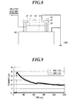
- FIG. 9 is a graph showing levels of cation movement under the temperatures of 200°C and 300°C and under an atmospheric pressure.
- the vertical axis of the graph of FIG. 9 represents the current generated by cation movement.
- the flow of current indicates occurrence of cation movement which indicates anodic bonding.
- the graph shows that a current of 0 ⁇ A flows, which means no cation movement occurs, under the temperature of 200°C.
- the graph thus shows that a temperature of about 200°C could not achieve anodic bonding that requires cation movement.
- Patent Literature 1 performs surface activated bonding as temporary bonding and then performs anodic bonding as main bonding. Such a method can make the temperature for anodic bonding lower than in the case of using anodic bonding alone.
- the technique of Patent Literature 1 nevertheless applies a high temperature of about not less than 200°C and not more than 400°C.
- a high temperature causes problems of deformation of the openings and breakages and warps of the plate members. It is thus difficult to perform bonding without impairing the discharge performance as described above.
- the surface activated bonding described in Patent Literature 2 can perform bonding at a further lower temperature than in the case of the anodic bonding described in Patent Literature 1.
- Such surface activated bonding gives rise to a problem when it is applied not to the bonding of wafer members as described in Patent Literature 2, but to the bonding of plate members having high-density multiple openings, such as nozzle holes, to form a droplet-discharging head substrate. That is, when a direct contact is made to the whole surface of a plate member for a droplet-discharging head substrate having high-density openings, such as nozzle holes, and a high pressure is applied to the surface, the nozzle holes may be damaged, broken or cracked. It is therefore difficult to employ the surface activated bonding for the droplet-discharging head substrate.
- a first aspect of the present invention is a method for manufacturing a droplet-discharging head substrate, the substrate including: a first plate having a plurality of nozzle holes to discharge droplets; and a second plate bonded to, of the first plate, a surface opposite to a droplet-discharging surface from which the droplets are discharged, the second plate having a plurality of through-holes communicating with the respective nozzle holes to form a plurality of flow paths, the method including: a first step to perform a surface activation process on joint surfaces of the first and second plates with an atom beam, an ion beam, or a plasma as an energy wave; a second step to align and stack the first and second plates in such a manner that the nozzle holes formed in the first plate communicate with the respective through-holes formed in the second plate; and a third step to bond the joint surfaces of the stacked first and second plates to each other by atomic bonding without covalent bonding caused by ion movement, wherein the third step to perform a surface activation process on
- a sum of a load applied in the third step of the first aspect is within a range of not less than 0.196 N and not more than 4.90 N.
- the third step of the first or second aspect is performed under a temperature of not less than 100°C and not more than 200°C.
- the first plate of the first to third aspects is made of silicon
- the second plate is made of glass
- the first and second plates each have a thickness of not less than 100 ⁇ m and not more than 300 ⁇ m.
- the droplet-discharging surface of the first plate of the first to fourth aspects has a liquid-repellent film formed thereon.
- a sixth aspect of the present invention is a method for manufacturing a droplet-discharging head, the head including: a first plate having a plurality of nozzle holes to discharge droplets; a second plate bonded to, of the first plate, a surface opposite to a droplet-discharging surface from which the droplets are discharged, the second plate having a plurality of through-holes communicating with the respective nozzle holes to form a plurality of flow paths; and a third plate bonded to, of the second plate, a surface opposite to a joint surface with the first plate, the third plate having a plurality of pressure chambers communicating with the respective through-holes, wherein a plurality of piezoelectric elements are disposed at positions corresponding to the respective pressure chambers, and pressures generated by volume changes of the respective pressure chambers in response to deformation of the respective piezoelectric elements allow liquid in the pressure chambers to be discharged through the nozzle holes in a form of the droplets, the method including: a first step to perform a surface activation process on
- a sum of a load applied in the third step of the sixth aspect is within a range of not less than 0.196 N and not more than 4.90 N.
- the third step of the sixth or seventh aspect is performed under a temperature of not less than 100°C and not more than 200°C.
- the first and third plates of the sixth to ninth aspects are each made of silicon, the second plate is made of glass, and the first, second, and third plates each have a thickness of not less than 100 ⁇ m and not more than 300 ⁇ m.
- the droplet-discharging surface of the first plate of the sixth to tenth aspects has a liquid-repellent film formed thereon.
- the present invention can provide a droplet-discharging head substrate and a droplet-discharging head produced by bonding without impairing good discharge characteristics.
- the present invention can also minimize warps, breakages, and damage of the plates constituting the droplet-discharging head substrate when the plates are bonded to each other.
- a droplet-discharging head and a droplet-discharging head substrate according to the present invention will now be described.
- FIG. 1 is an exploded perspective view of a droplet-discharging head according to the present invention.
- FIG. 2 is a partial cross-sectional view showing the layer configuration of a droplet-discharging head substrate 2 in the droplet-discharging head shown in FIG. 1 .
- the reference number 1 refers to a droplet-discharging head.
- the droplet-discharging head 1 includes a droplet-discharging head substrate 2, a retaining substrate 3, an external wiring member 4, and ink flow path members 5.
- the droplet-discharging head substrate 2 is constituted of three plates, a nozzle plate 21 (first plate), an intermediate plate 22 (second plate) , and a body plate 23 (third plate).
- the three plates are stacked and integrated with one another to form the droplet-discharging head substrate 2.
- the nozzle plate 21 is made of an Si plate having a thickness of about not less than 100 ⁇ m and not more than 300 ⁇ m.
- the nozzle plate 21 has nozzle holes 211 to discharge ink droplets.
- the nozzle holes 211 are disposed at positions corresponding to respective communication holes 221 of the intermediate plate 22 when the plates 21 and 22 are stacked.
- the nozzle holes 211 are formed on the side, remote from the intermediate plate 22, of the nozzle plate 21.
- the nozzle plate 21 has openings (large-diameter parts 212), which correspond to the respective nozzle holes 211, on the side adjacent to the intermediate plate 22.
- the large-diameter parts 212 are recesses having a larger diameter than the nozzle holes 211 and communicate with the respective nozzle hole 211.
- the nozzle plate 21 has a liquid-repellent film (not shown) on the plane 210 on which the nozzle holes 211 are formed (i.e., nozzle plane).
- the liquid-repellent film can enhance the ejection stability of the droplet-discharging head.
- a suitable liquid-repellent film is preferably formed in accordance with the droplets to be discharged from the nozzle holes.
- fluorine resin such as OPTOOL is preferred if the droplets to be discharged are ink droplets.
- the upper temperature limit of the liquid-repellent film, such as OPTOOL, formed on the nozzle plate 21 is generally 200°C or less.
- the manufacturing method according to the present invention can perform bonding to form the droplet-discharging head substrate at 200°C or less.
- the bonding after the formation of the above-described liquid-repellent film on the nozzle plate 21 does not impair the good liquid-repellent performance, enhancing ejection stability of the droplet-discharging head.
- anodic bonding which involves a high temperature of over the upper temperature limit of the liquid-repellent film (i.e.
- the liquid-repellent film deteriorates, failing to provide good ejection stability of the droplet-discharging head.
- the intermediate plate 22 is made of a glass plate having the same shape as the body plate 23 in a plan view and having a thickness of about not less than 100 ⁇ m and not more than 300 ⁇ m.
- the intermediate plate 22 has communication holes 221.
- the communication holes 221 are disposed at the positions corresponding to extended parts 231a of respective pressure chambers 231 in the body plate 23.
- the communication holes 221 extend through the entire thickness of the intermediate plate 22 and serve as ink flow paths at the time of ink discharge.
- the body plate 23 which has a long side along the A direction in FIG. 1 , is made of an Si plate having a thickness of about not less than 100 ⁇ m and not more than 300 ⁇ m.
- the body plate 23 is a flow-path formation plate having depressed pressure chambers 231, common flow paths 232, and ink supply paths 233.
- the pressure chambers 231, the common flow paths 232, and the ink supply paths 233 are formed by etching one face (the lower face in FIG. 1 ) of the body plate 23.
- the pressure chambers 231 are substantially circular in shape in a plan view.
- Each of the common flow paths 232 is a common groove to supply ink to a plurality of pressure chambers 231.
- Each of the ink supply paths 233 is a fine groove which individually communicates with a common flow path 232 and a pressure chamber 231 and supplies ink in the common flow path 232 to the pressure chamber 231.
- each pressure chamber 231 extends outward to form an extended part 231a.
- the extended parts 231a are communication sections to communicate with the communication holes 221 formed in the intermediate plate 22 described above.
- FIG. 1 shows the body plate 23 having sixteen pressure chambers 231 arranged in the A direction.
- Two common flow paths 232 are disposed with the array of the pressure chambers 231 between the two common flow paths 232.
- Each of the two common flow paths 232 is to supply ink to eight pressure chambers 231 (every other pressure chambers 231).
- the other face (the upper face in FIG. 1 ) of the body plate 23 has piezoelectric elements 234 disposed thereon.
- the piezoelectric elements 234 are pressure generators made of, for example, PZT, disposed corresponding to the positions of the respective pressure chambers 231. Deformation of the piezoelectric elements 234 deforms the deformable walls 235 between the piezoelectric elements 234 and the pressure chambers 231 to apply pressures to the ink in the pressure chambers 231 to discharge the ink.
- Each of the piezoelectric elements 234 has electrodes (not shown) on its upper and lower faces. The upper electrode is an individual electrode, whereas the lower electrode is in contact with a common electrode disposed on the upper face of the body plate 23.
- Each of the common flow paths 232 extends in the A direction, which is the longitudinal direction of the body plate 23.
- the end parts of each common flow path 232 communicate with through-holes 236, which extend through the entire thickness of the body plate 23, near the both ends of the body plate 23 in the A direction.
- Two through-holes 236 are arranged along the B direction, which is a short-side direction of the body plate 23 perpendicular to the A direction, at each end part of the body plate 23.
- Each of the through-holes 236 communicates with an end of a common flow path 232.
- the liquid to be discharged by the droplet-discharging head is ink.
- the liquid according to the present invention is not limited to ink.
- the droplet-discharging head may discharge, for example, liquid containing metal for forming semiconductor circuits as well as UV inks and water-soluble inks.
- the head substrate is constituted of only three plate members, the nozzle plate 21, the intermediate plate 22, and the body plate 23. It should be understood, however, that the head substrate may be a stack of four or more plate members.
- the method for manufacturing the droplet-discharging head substrate according to the present invention will now be described in detail with reference to the droplet-discharging head substrate shown in FIG. 1 as an example.
- the manufacturing method includes the following processes (see FIG. 3 ).
- the surface activation process is performed by irradiation of joint surfaces with an atom beam, an ion beam, or a plasma as an energy wave.
- the surface activation process adds OH groups or ON groups through chemical processing using a plasma, such as a nitrogen plasma or an oxygen plasma.
- the joint surfaces may be irradiated with an Ar ion beam to be activated and then may react with water molecules in the atmosphere for OH groups to be added to the joint surfaces.
- the nozzle plate 21, the intermediate plate 22, and the body plate 23 are arranged on an irradiation table 71 below a plasma generator 70 under a reduced pressure, as shown in FIG. 4 , for the joint surfaces to be irradiated with an oxygen or nitrogen plasma.
- the irradiation of plasma causes OH or ON groups to adhere to the surfaces of Si (silicon) , i. e. , the joint surf aces of the nozzle plate 21, the intermediate plate 22, and the body plate 23, making the joint surfaces hydrophilic.
- the plates on which the surface activation process has been performed are aligned in such a manner that the through-holes of the nozzle plate 21, the communication holes of the intermediate plate 22, and the through-holes of the body plate 23 communicate with each other.
- the plates are then stacked.
- the alignment process is performed by an operator handling the plates while watching alignment marks (not shown) on the corners of each plate using, for example, a CCD camera.
- the alignment marks are put in advance before the stacking and alignment process at such locations that the through-holes of the nozzle plate 21, the communication holes of the intermediate plate 22, and the through-holes of the body plate 23 will communicate with each other when the plates 21, 22, and 23 are stacked.
- two cut holes are made at corners of each plate by etching to be used as the alignment marks.
- the device is constituted of a base 64, fixation members 61, support members 63, and elastic members 65.
- the base 64 is a place where the nozzle plate 21, the intermediate plate 22, and the body plate 23 are to be placed and to which the support members 63 are fixed.
- Commonly-used metal or a conductive member that does not deform in response to heat at the time of electrostatic attraction may be used as the base 64.
- the fixation members 61 clamp the both-end parts of the nozzle plate 21, the intermediate plate 22, and the body plate 23 to fix them between the fixation members 61 and the base 64 so that the plates 21, 22, and 23 do not go out of alignment in the subsequent bonding process 2 (see FIGS. 5A and 5C ).
- the both-end parts are outside of a nozzle-hole formation area a of the nozzle plate 21 (i.e., outside of the area formed by a plurality of nozzle holes extending in the longitudinal direction of the nozzle plate 21; see FIG. 1 ).
- the support members 63 support the fixation members 61 and include the elastic members 65.
- the elastic restoring force of the elastic members 65 When the stack of the nozzle plate 21, the intermediate plate 22, and the body plate 23 held by the fixation members is higher than the level of the elastic members supported by the fixation members, the elastic restoring force of the elastic members 65 generates a force for pressing the nozzle plate toward the body plate.
- the fixation members 61 thus press the both ends of each of the stacked plates to fix the plates.
- the above-described fixing process is a process where the both ends of the plates are pressed by the fixation members for fixation.
- the fixing process may be performed through any other method that can fix the plates so that the aligned and stacked plates do not go out of alignment in the processes described later.
- alignment frames (not shown) may be provided at two diagonal corners of the four corners of the plates to prevent a displacement in the direction perpendicular to the stacking direction.
- the load application process is a process to mainly apply a pressure to the plates to straighten the warps of the plates. It is not that the joint surfaces are brought close to and bonded to each other in this process alone, but that this process brings the joint surfaces of the plates close enough for the bonding to each other in combination with the electrostatic attraction described later.
- the warps can naturally be straightened. If, however, a load is applied to the whole surface of the plate, the nozzle-hole formation area a is subjected to the load, leading to damage of the nozzle-hole formation area a.
- load members are placed on an area away from the nozzle-hole formation area a in such a manner that a load is evenly applied to the area away from the nozzle-hole formation area a, as shown in FIG. 7 . If the load members are disposed so as to evenly apply a load to the area away from the nozzle-hole formation area a, an inherent convex warp in the center of each plate can be straightened with less load.
- the nozzles are not subject to damage that would affect the discharge characteristics. Further, the load application process performed under the atmospheric pressure can let air escape through the through-holes at the time of bonding. This allows the joint surfaces to come close to each other to achieve bonding necessary for the manufacture of the droplet-discharging head substrate.
- the load that can straighten the warps of the members themselves is enough. The load required to straighten the warps of the members themselves varies depending to the thicknesses of the members.
- a pressure of not less than 0.196 N and not more than 4.90 N is preferably applied to the plates when each of the plates has a thickness of not less than 100 ⁇ m and not more than 300 ⁇ m and has a surface area of not less than 480 mm 2 and not more than 550 mm 2 .
- the load to straighten the warp inherent in each plate can be reduced and damage to the nozzles and breakages of the plates can be prevented.
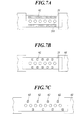
- FIGS. 7A to 7C There are various layouts of load members 62 that can straighten the warps and where the load members 62 are disposed away from the nozzle-hole formation area a as shown in FIGS. 7A to 7C .
- the layout of FIG. 7A is preferred in that plate-like load members 62 disposed in such a manner as to avoid the nozzle-hole formation area a can apply a load evenly to the area away from the nozzle-hole formation area a.
- FIG. 7B is preferred in that a load is evenly applied to the area away from the nozzle-hole formation area a while the contact area between the load members and the nozzle plate is minimized.
- FIG. 7A is preferred in that a load is evenly applied to the area away from the nozzle-hole formation area a while the contact area between the load members and the nozzle plate is minimized.
- the load members 62 may be made of various types of material, such as commonly-used metal. Each of the load members may have a plate-like shape as shown in FIG. 7A . Alternatively, in the case of high-density openings, a needle load member 621 as shown in FIG. 6 may be disposed in such a manner as not to touch the openings.
- the needle load member 621 is constituted of needle parts 622 and a base part 623.
- the needle parts 622 and the base part 623 are preferably made of material, such as metal, that does not deform due to heat applied at the time of electrostatic attraction.
- the needle load member 621 is designed so that the load members can be evenly placed on the area away from the nozzle-hole formation area a in accordance with the arrangement pattern of the nozzle openings. Such a needle load member 621 can collectively apply the load members, leading to enhanced production efficiency than in the case in which a plurality of load members are placed one by one.
- a needle load member 621 is preferably used for a nozzle plate having high-density nozzles which requires a load member to be finely divided so that a load is applied evenly to the area away from the nozzle-hole formation area a.
- the intermediate plate 22 is connected to a negative electric potential, and the nozzle plate 21 and the body plate 23 are connected to the GND.
- the intermediate plate 22 has a lower electric potential than the nozzle plate 21 and the body plate 23, while the nozzle plate 21 and the body plate 23, which are connected to the GND, have a higher electric potential.
- the difference in electric potential generates an electrostatic attractive force for the molecules on one plate to come close to the molecules on another plate in the stacked plates.
- the electrostatic attractive force consequently causes the plates to attract each other, and the air remaining in the gaps is discharged through the flow paths extending from the body plate to the nozzles.
- This causes the plates to come as close to each other as a distance of several hundred nm.
- the Van der Waals force causes OH or ON groups to come into contact with each other at the molecular level to create hydrogen bonds and enables the surface activated bonding. If the plates have small surface roughness that creates gaps between the plates, the bonding is preferably performed under the condition of not less than 100°C and not more than 200°C.
- the electrostatic attraction according to the present invention removes the gaps between the plates using an electrostatic attractive force without the need for contact with the members and brings the plates close to each other enough for the subsequent bonding of the plates by atomic bonding.
- the electrostatic attraction does not require a high pressure for bonding that would be necessary for typical surface activated bonding.
- the electrostatic attraction in combination with the load application process, which is a previous step, can minimize the breakages, warps, and damage of the surfaces of the plate members.
- the electrostatic attraction is performed under the condition of direct-current high voltage of not less than 500 V and not more than 2000 V and under ordinary pressure . Further, while anodic bonding requires a high voltage and a temperature of at least 250°C, the bonding using the electrostatic attraction can be performed at a lower temperature and thus can prevent the plates from warping again. Specifically, the bonding using the electrostatic attraction can be performed under a temperature of not less than 100°C and not more than 200°C even if the plate surfaces have small roughness as described above.
- the combination of the load application process and the electrostatic attraction process of the bonding process 2, where load members necessary for straightening warps are placed at such positions as not to damage the nozzles and where the gaps formed due to the small roughness between the plates are filled using the electrostatic attraction, can bond the plates to each other in such a manner as to minimize the warps, breakages, and damage of the plates constituting the droplet-discharging head substrate.
- an electrostatic attractive force without involving ion movement enables the bonding without the need for expensive glass for anodic bonding, such as borosilicate glass (TEMPAX glass) and glass for anodic bonding of SW series, as the intermediate plate 22.
- glass for anodic bonding such as borosilicate glass (TEMPAX glass) and glass for anodic bonding of SW series, as the intermediate plate 22.
- glass, other than the glass for anodic bonding, which is applicable to the bonding method according to the present invention include soda-lime glass. Such soda-lime glass is lower in price than the glass for anodic bonding, leading to reduction in manufacturing cost.
- a surface activation process and a layout of load members of the present invention are not limited to those of the above-described embodiment.
- the bonding method according to the present invention is used for all the bonding of the joint surfaces of the nozzle plate, the intermediate plate, and the body plate for sake of simplicity.
- the present invention is not limited to this.
- the scope of the present invention also includes a case in which the nozzle plate and the intermediate plate are bonded to each other in the bonding method according to the present invention whereas the intermediate plate and the body plate are bonded to each other in a conventional bonding method, such as adhesion bonding or anodic bonding, to form a droplet-discharging head substrate.
- the present invention is applicable to a field of manufacturing droplet-discharging head substrates and droplet-discharging heads to discharge liquid from nozzle holes.
Landscapes
- Engineering & Computer Science (AREA)
- Manufacturing & Machinery (AREA)
- Particle Formation And Scattering Control In Inkjet Printers (AREA)
Abstract
Description
- The present invention relates to a method for manufacturing a droplet-discharging head substrate and a droplet-discharging head to discharge liquid from nozzle holes.
- In recent years, a so-called droplet-discharging technology is used for print apparatuses, such as printers, and deposition apparatuses for manufacturing semiconductor devices. The droplet-discharging technology allows discharge and throw of droplets, such as ink and deposition material for deposition apparatuses, onto targets.
- Enhanced quality of printed images or accuracy of deposition is expected for such a droplet-discharging technology, and accordingly, droplet-discharging heads used for the droplet-discharging technology should have discharge characteristics that enable accurate ejection of very small droplets onto targets. Further, in accordance with recent reduction in size and increase in resolution of droplet-discharging heads, there has been a need for droplet-discharging heads having high-density nozzles to discharge droplets and at the same time having good discharge characteristics. The manufacture of droplet-discharging head substrates with high-density nozzle holes requires high processing accuracy for alignment and bonding of the plates constituting the substrates.
- An example of such droplet-discharging head substrates is shown in
FIG. 1 , which is an exploded perspective view of a droplet-discharging head. The droplet-discharginghead substrate 2 is constituted of anozzle plate 21, anintermediate plate 22, and abody plate 23. Thenozzle plate 21 has high-density nozzle holes 211. Theintermediate plate 22 hascommunication holes 221 to communicate with therespective nozzle holes 211 to form flow paths. Thebody plate 23 has flow paths to communicate with the respective through-holes individually and has pressure chambers communicating with the flow paths and havingpiezoelectric elements 234 to discharge droplets at relevant positions. Accurate bonding of these plates is necessary for the discharge head to have good discharge characteristics. - A conventional method for bonding the plates uses an adhesive agent to bond the joint surfaces to each other. Bonding with an adhesive agent, however, has a risk that the adhesive agent may cover the openings formed in the plates and thus may affect the discharge characteristics. Such a risk is especially high for a droplet-discharging head substrate having high-density openings, such as nozzle holes and flow paths.
- In view of this, there have been bonding methods without using an adhesive agent, such as anodic bonding and surface activated bonding where the surfaces of members are activated at a lower temperature than in anodic bonding for bonding the surfaces to each other.
- The anodic bonding is a method using covalent bonding caused by the movement of cation contained in a glass plate. Such a method can bond members tightly without the need for an adhesive agent as disclosed in, for example,
Patent Literature 1. In the case of formation of a droplet-discharging head by bonding an Si plate and glass member by anodic bonding as inPatent Literature 1, a high temperature of 300°C or higher needs to be applied for cation movement while joint surfaces are softened and brought closed to each other. - The surface activated bonding is a method where the joint surfaces of a silicon substrate and a glass substrate are irradiated with an atom beam, an ion beam, or a plasma as an energy wave to be activated for OH or ON groups to be added to the joint surfaces and then the substrates are bonded to each other by atomic bonding between the substrates. Similarly to the anodic bonding, the surface activated bonding can bond joint surfaces with each other without using an adhesive agent as disclosed in
Patent Literature 2. Instead of the ion movement requiring a high temperature as in the anodic bonding, the surface activated bonding needs to press the plates against each other with a high pressure while softening the joint surfaces under the above-mentioned low temperature for the joint surfaces to come close to and bond to each other. -
- Patent Literature 1: Japanese Unexamined Patent Application Publication No.
2005-187321 - Patent Literature 2: Japanese Unexamined Patent Application Publication No.
2003-318217 - In typical anodic bonding as used in
Patent Literature 1, a combination of direct-current high voltage application and high-temperature heating is necessary to soften joint surfaces, to bring the joint surfaces into tight contact with each other, and to cause cation movement as described above. Specifically, while the plates are in contact with each other, a direct-current high voltage is applied with the glass plate side being a cathode, and a high temperature of about not less than 300°C and not more than 500°C is applied.FIG. 9 is a graph showing levels of cation movement under the temperatures of 200°C and 300°C and under an atmospheric pressure. The vertical axis of the graph ofFIG. 9 represents the current generated by cation movement. The flow of current indicates occurrence of cation movement which indicates anodic bonding. The graph shows that a current of 0 µA flows, which means no cation movement occurs, under the temperature of 200°C. The graph thus shows that a temperature of about 200°C could not achieve anodic bonding that requires cation movement. - The technique of
Patent Literature 1 performs surface activated bonding as temporary bonding and then performs anodic bonding as main bonding. Such a method can make the temperature for anodic bonding lower than in the case of using anodic bonding alone. The technique ofPatent Literature 1 nevertheless applies a high temperature of about not less than 200°C and not more than 400°C. When plate members with high-density multiple openings, such as nozzle holes, are to be bonded to each other to form a droplet-discharging head, such a high temperature causes problems of deformation of the openings and breakages and warps of the plate members. It is thus difficult to perform bonding without impairing the discharge performance as described above. - The surface activated bonding described in
Patent Literature 2 can perform bonding at a further lower temperature than in the case of the anodic bonding described inPatent Literature 1. Such surface activated bonding, however, gives rise to a problem when it is applied not to the bonding of wafer members as described inPatent Literature 2, but to the bonding of plate members having high-density multiple openings, such as nozzle holes, to form a droplet-discharging head substrate. That is, when a direct contact is made to the whole surface of a plate member for a droplet-discharging head substrate having high-density openings, such as nozzle holes, and a high pressure is applied to the surface, the nozzle holes may be damaged, broken or cracked. It is therefore difficult to employ the surface activated bonding for the droplet-discharging head substrate. - It is an object of the present invention to provide a bonding method that can bond stacked plates to each other to manufacture a droplet-discharging head substrate without damaging nozzle holes and without impairing a good discharge performance.
- In order to solve the above-described problems, a first aspect of the present invention is a method for manufacturing a droplet-discharging head substrate, the substrate including: a first plate having a plurality of nozzle holes to discharge droplets; and a second plate bonded to, of the first plate, a surface opposite to a droplet-discharging surface from which the droplets are discharged, the second plate having a plurality of through-holes communicating with the respective nozzle holes to form a plurality of flow paths, the method including: a first step to perform a surface activation process on joint surfaces of the first and second plates with an atom beam, an ion beam, or a plasma as an energy wave; a second step to align and stack the first and second plates in such a manner that the nozzle holes formed in the first plate communicate with the respective through-holes formed in the second plate; and a third step to bond the joint surfaces of the stacked first and second plates to each other by atomic bonding without covalent bonding caused by ion movement, wherein the third step bonds the joint surfaces by bringing a load member into contact with the droplet-discharging surface of the first plate at a position away from the nozzle holes and applying a pressure to the droplet-discharging surface under an atmospheric pressure, and by bringing the joint surfaces close to each other with an electrostatic attractive force generated between the joint surfaces.
- In a second aspect, a sum of a load applied in the third step of the first aspect is within a range of not less than 0.196 N and not more than 4.90 N.
- In a third aspect, the third step of the first or second aspect is performed under a temperature of not less than 100°C and not more than 200°C.
- In a fourth aspect, the first plate of the first to third aspects is made of silicon, the second plate is made of glass, and the first and second plates each have a thickness of not less than 100 µm and not more than 300 µm.
- In a fifth aspect, the droplet-discharging surface of the first plate of the first to fourth aspects has a liquid-repellent film formed thereon.
- A sixth aspect of the present invention is a method for manufacturing a droplet-discharging head, the head including: a first plate having a plurality of nozzle holes to discharge droplets; a second plate bonded to, of the first plate, a surface opposite to a droplet-discharging surface from which the droplets are discharged, the second plate having a plurality of through-holes communicating with the respective nozzle holes to form a plurality of flow paths; and a third plate bonded to, of the second plate, a surface opposite to a joint surface with the first plate, the third plate having a plurality of pressure chambers communicating with the respective through-holes, wherein a plurality of piezoelectric elements are disposed at positions corresponding to the respective pressure chambers, and pressures generated by volume changes of the respective pressure chambers in response to deformation of the respective piezoelectric elements allow liquid in the pressure chambers to be discharged through the nozzle holes in a form of the droplets, the method including: a first step to perform a surface activation process on joint surfaces of the first, second, and third plates with an atom beam, an ion beam, or a plasma as an energy wave; a second step to align and stack the first, second, and third plates in such a manner that the nozzle holes formed in the first plate communicate with the respective through-holes formed in the second plate; and a third step to bond the joint surfaces of the stacked first, second, and third plates to each other by atomic bonding without covalent bonding caused by ion movement, wherein the third step bonds the joint surfaces by bringing a load member into contact with the droplet-discharging surface of the first plate at a position away from the nozzle holes and applying a pressure to the droplet-discharging surface under an atmospheric pressure, and by bringing the joint surfaces close to each other with an electrostatic attractive force generated between the joint surfaces.
- In a seventh aspect, a sum of a load applied in the third step of the sixth aspect is within a range of not less than 0.196 N and not more than 4.90 N.
- In an eighth aspect, the third step of the sixth or seventh aspect is performed under a temperature of not less than 100°C and not more than 200°C.
- In a ninth aspect, the first and third plates of the sixth to ninth aspects are each made of silicon, the second plate is made of glass, and the first, second, and third plates each have a thickness of not less than 100 µm and not more than 300 µm.
- In a tenth aspect, the droplet-discharging surface of the first plate of the sixth to tenth aspects has a liquid-repellent film formed thereon.
- The present invention can provide a droplet-discharging head substrate and a droplet-discharging head produced by bonding without impairing good discharge characteristics. The present invention can also minimize warps, breakages, and damage of the plates constituting the droplet-discharging head substrate when the plates are bonded to each other.
-
-
FIG. 1 is an exploded perspective view of a droplet-discharging head according to the present invention; -
FIG. 2 is a partial cross-sectional view showing the layer configuration of a head substrate in the droplet-discharging head shown inFIG. 1 ; -
FIG. 3 is a flowchart of the method for manufacturing the head substrate according to the present invention; -
FIG. 4 is a schematic view to show a surface activation process; -
FIG. 5A is a side view to schematically show the state before application of a load for sticking the plates together; -
FIG. 5B is an enlarged side view of the stacked plates ofFIG. 5A ; -
FIG. 5C is a side view to schematically show the state in which a load is applied to stick the plates together; -
FIG. 5D is an enlarged side view of the stacked plates ofFIG. 5C ; -
FIG. 6 is a schematic view of a needle load member; -
FIG. 7A is a top view schematically showing the configuration with load members applied to stick the plates together; -
FIG. 7B is a top view schematically showing the configuration with load members applied to stick the plates together; -
FIG. 7C is a top view schematically showing the configuration with load members applied to stick the plates together; -
FIG. 8 is a schematic view to show electrostatic attraction; and -
FIG. 9 shows changes in cation movement depending on temperature. - A droplet-discharging head and a droplet-discharging head substrate according to the present invention will now be described.
-
FIG. 1 is an exploded perspective view of a droplet-discharging head according to the present invention.FIG. 2 is a partial cross-sectional view showing the layer configuration of a droplet-discharginghead substrate 2 in the droplet-discharging head shown inFIG. 1 . - The descriptions will now be made with reference to
FIGS. 1 and2 . - In
FIG. 1 , thereference number 1 refers to a droplet-discharging head. The droplet-discharginghead 1 includes a droplet-discharginghead substrate 2, a retainingsubstrate 3, anexternal wiring member 4, and inkflow path members 5. - The droplet-discharging
head substrate 2 is constituted of three plates, a nozzle plate 21 (first plate), an intermediate plate 22 (second plate) , and a body plate 23 (third plate). The three plates are stacked and integrated with one another to form the droplet-discharginghead substrate 2. - The
nozzle plate 21 is made of an Si plate having a thickness of about not less than 100 µm and not more than 300 µm. Thenozzle plate 21 hasnozzle holes 211 to discharge ink droplets. The nozzle holes 211 are disposed at positions corresponding torespective communication holes 221 of theintermediate plate 22 when theplates intermediate plate 22, of thenozzle plate 21. Thenozzle plate 21 has openings (large-diameter parts 212), which correspond to the respective nozzle holes 211, on the side adjacent to theintermediate plate 22. The large-diameter parts 212 are recesses having a larger diameter than the nozzle holes 211 and communicate with therespective nozzle hole 211. - The
nozzle plate 21 has a liquid-repellent film (not shown) on theplane 210 on which the nozzle holes 211 are formed (i.e., nozzle plane). The liquid-repellent film can enhance the ejection stability of the droplet-discharging head. In order to enhance the ejection stability of the droplet-discharging head, a suitable liquid-repellent film is preferably formed in accordance with the droplets to be discharged from the nozzle holes. For example, fluorine resin, such as OPTOOL is preferred if the droplets to be discharged are ink droplets. - If the droplets to be discharged are ink droplets as mentioned above, the upper temperature limit of the liquid-repellent film, such as OPTOOL, formed on the
nozzle plate 21 is generally 200°C or less. The manufacturing method according to the present invention can perform bonding to form the droplet-discharging head substrate at 200°C or less. Thus the bonding after the formation of the above-described liquid-repellent film on thenozzle plate 21 does not impair the good liquid-repellent performance, enhancing ejection stability of the droplet-discharging head. If anodic bonding, which involves a high temperature of over the upper temperature limit of the liquid-repellent film (i.e. , 200°C or less) , were used to form the droplet-discharging head substrate after the formation of the liquid-repellent film, the liquid-repellent film deteriorates, failing to provide good ejection stability of the droplet-discharging head. - The
intermediate plate 22 is made of a glass plate having the same shape as thebody plate 23 in a plan view and having a thickness of about not less than 100 µm and not more than 300 µm. Theintermediate plate 22 has communication holes 221. When theintermediate plate 22 and thebody plate 23 are stacked, the communication holes 221 are disposed at the positions corresponding toextended parts 231a ofrespective pressure chambers 231 in thebody plate 23. The communication holes 221 extend through the entire thickness of theintermediate plate 22 and serve as ink flow paths at the time of ink discharge. - The
body plate 23, which has a long side along the A direction inFIG. 1 , is made of an Si plate having a thickness of about not less than 100 µm and not more than 300 µm. Thebody plate 23 is a flow-path formation plate havingdepressed pressure chambers 231,common flow paths 232, andink supply paths 233. Thepressure chambers 231, thecommon flow paths 232, and theink supply paths 233 are formed by etching one face (the lower face inFIG. 1 ) of thebody plate 23. Thepressure chambers 231 are substantially circular in shape in a plan view. Each of thecommon flow paths 232 is a common groove to supply ink to a plurality ofpressure chambers 231. Each of theink supply paths 233 is a fine groove which individually communicates with acommon flow path 232 and apressure chamber 231 and supplies ink in thecommon flow path 232 to thepressure chamber 231. - A part of each
pressure chamber 231 extends outward to form anextended part 231a. Theextended parts 231a are communication sections to communicate with the communication holes 221 formed in theintermediate plate 22 described above.FIG. 1 shows thebody plate 23 having sixteenpressure chambers 231 arranged in the A direction. Twocommon flow paths 232 are disposed with the array of thepressure chambers 231 between the twocommon flow paths 232. Each of the twocommon flow paths 232 is to supply ink to eight pressure chambers 231 (every other pressure chambers 231). - The other face (the upper face in
FIG. 1 ) of thebody plate 23 haspiezoelectric elements 234 disposed thereon. Thepiezoelectric elements 234 are pressure generators made of, for example, PZT, disposed corresponding to the positions of therespective pressure chambers 231. Deformation of thepiezoelectric elements 234 deforms thedeformable walls 235 between thepiezoelectric elements 234 and thepressure chambers 231 to apply pressures to the ink in thepressure chambers 231 to discharge the ink. Each of thepiezoelectric elements 234 has electrodes (not shown) on its upper and lower faces. The upper electrode is an individual electrode, whereas the lower electrode is in contact with a common electrode disposed on the upper face of thebody plate 23. - Each of the
common flow paths 232 extends in the A direction, which is the longitudinal direction of thebody plate 23. The end parts of eachcommon flow path 232 communicate with through-holes 236, which extend through the entire thickness of thebody plate 23, near the both ends of thebody plate 23 in the A direction. Two through-holes 236 are arranged along the B direction, which is a short-side direction of thebody plate 23 perpendicular to the A direction, at each end part of thebody plate 23. Each of the through-holes 236 communicates with an end of acommon flow path 232. - In the above described example, the liquid to be discharged by the droplet-discharging head is ink. The liquid according to the present invention, however, is not limited to ink. The droplet-discharging head may discharge, for example, liquid containing metal for forming semiconductor circuits as well as UV inks and water-soluble inks.
- In the above described example, the head substrate is constituted of only three plate members, the
nozzle plate 21, theintermediate plate 22, and thebody plate 23. It should be understood, however, that the head substrate may be a stack of four or more plate members. - The method for manufacturing the droplet-discharging head substrate according to the present invention will now be described in detail with reference to the droplet-discharging head substrate shown in
FIG. 1 as an example. The manufacturing method includes the following processes (seeFIG. 3 ). - (1) Surface activation process
- (2) Stacking and alignment process
- (3) Fixing process
- (4) Load application process
- (5) Electrostatic attraction process
- The processes will now be described in detail.
- The surface activation process is performed by irradiation of joint surfaces with an atom beam, an ion beam, or a plasma as an energy wave. For example, the surface activation process adds OH groups or ON groups through chemical processing using a plasma, such as a nitrogen plasma or an oxygen plasma. As an alternative method, the joint surfaces may be irradiated with an Ar ion beam to be activated and then may react with water molecules in the atmosphere for OH groups to be added to the joint surfaces.
- In the surface activation process, the
nozzle plate 21, theintermediate plate 22, and thebody plate 23 are arranged on an irradiation table 71 below aplasma generator 70 under a reduced pressure, as shown inFIG. 4 , for the joint surfaces to be irradiated with an oxygen or nitrogen plasma. The irradiation of plasma causes OH or ON groups to adhere to the surfaces of Si (silicon) , i. e. , the joint surf aces of thenozzle plate 21, theintermediate plate 22, and thebody plate 23, making the joint surfaces hydrophilic. - The plates on which the surface activation process has been performed are aligned in such a manner that the through-holes of the
nozzle plate 21, the communication holes of theintermediate plate 22, and the through-holes of thebody plate 23 communicate with each other. The plates are then stacked. The alignment process is performed by an operator handling the plates while watching alignment marks (not shown) on the corners of each plate using, for example, a CCD camera. The alignment marks are put in advance before the stacking and alignment process at such locations that the through-holes of thenozzle plate 21, the communication holes of theintermediate plate 22, and the through-holes of thebody plate 23 will communicate with each other when theplates - The fixing process will now be described with reference to
FIG. 5 . - The device is constituted of a
base 64,fixation members 61,support members 63, andelastic members 65. Thebase 64 is a place where thenozzle plate 21, theintermediate plate 22, and thebody plate 23 are to be placed and to which thesupport members 63 are fixed. Commonly-used metal or a conductive member that does not deform in response to heat at the time of electrostatic attraction may be used as thebase 64. - The
fixation members 61 clamp the both-end parts of thenozzle plate 21, theintermediate plate 22, and thebody plate 23 to fix them between thefixation members 61 and the base 64 so that theplates FIGS. 5A and5C ). The both-end parts are outside of a nozzle-hole formation area a of the nozzle plate 21 (i.e., outside of the area formed by a plurality of nozzle holes extending in the longitudinal direction of thenozzle plate 21; seeFIG. 1 ). Thesupport members 63 support thefixation members 61 and include theelastic members 65. When the stack of thenozzle plate 21, theintermediate plate 22, and thebody plate 23 held by the fixation members is higher than the level of the elastic members supported by the fixation members, the elastic restoring force of theelastic members 65 generates a force for pressing the nozzle plate toward the body plate. Thefixation members 61 thus press the both ends of each of the stacked plates to fix the plates. - The above-described fixing process is a process where the both ends of the plates are pressed by the fixation members for fixation. The fixing process, however, may be performed through any other method that can fix the plates so that the aligned and stacked plates do not go out of alignment in the processes described later. For example, alignment frames (not shown) may be provided at two diagonal corners of the four corners of the plates to prevent a displacement in the direction perpendicular to the stacking direction.
- The load application process is a process to mainly apply a pressure to the plates to straighten the warps of the plates. It is not that the joint surfaces are brought close to and bonded to each other in this process alone, but that this process brings the joint surfaces of the plates close enough for the bonding to each other in combination with the electrostatic attraction described later.
- If a load is applied to the whole surface of the plate, the warps can naturally be straightened. If, however, a load is applied to the whole surface of the plate, the nozzle-hole formation area a is subjected to the load, leading to damage of the nozzle-hole formation area a. In view of this, load members are placed on an area away from the nozzle-hole formation area a in such a manner that a load is evenly applied to the area away from the nozzle-hole formation area a, as shown in
FIG. 7 . If the load members are disposed so as to evenly apply a load to the area away from the nozzle-hole formation area a, an inherent convex warp in the center of each plate can be straightened with less load. Since the contact area between the load members and the nozzle plate is reduced as described above, the nozzles are not subject to damage that would affect the discharge characteristics. Further, the load application process performed under the atmospheric pressure can let air escape through the through-holes at the time of bonding. This allows the joint surfaces to come close to each other to achieve bonding necessary for the manufacture of the droplet-discharging head substrate. The load that can straighten the warps of the members themselves is enough. The load required to straighten the warps of the members themselves varies depending to the thicknesses of the members. For example, a pressure of not less than 0.196 N and not more than 4.90 N is preferably applied to the plates when each of the plates has a thickness of not less than 100 µm and not more than 300 µm and has a surface area of not less than 480 mm2 and not more than 550 mm2. Thus, the load to straighten the warp inherent in each plate can be reduced and damage to the nozzles and breakages of the plates can be prevented. - There are various layouts of
load members 62 that can straighten the warps and where theload members 62 are disposed away from the nozzle-hole formation area a as shown inFIGS. 7A to 7C . In particular, the layout ofFIG. 7A is preferred in that plate-like load members 62 disposed in such a manner as to avoid the nozzle-hole formation area a can apply a load evenly to the area away from the nozzle-hole formation area a. The layout ofFIG. 7B is preferred in that a load is evenly applied to the area away from the nozzle-hole formation area a while the contact area between the load members and the nozzle plate is minimized. The layout ofFIG. 7C , where theload members 62 are arranged in a zigzag fashion with the nozzle-hole formation area a therebetween, is more preferred in that a load is evenly applied to the area away from the nozzle-hole formation area a and in that the contact area between the load members and the nozzle plate is smaller compared to the layout ofFIG. 7B . - The
load members 62 may be made of various types of material, such as commonly-used metal. Each of the load members may have a plate-like shape as shown inFIG. 7A . Alternatively, in the case of high-density openings, aneedle load member 621 as shown inFIG. 6 may be disposed in such a manner as not to touch the openings. Theneedle load member 621 is constituted ofneedle parts 622 and abase part 623. Theneedle parts 622 and thebase part 623 are preferably made of material, such as metal, that does not deform due to heat applied at the time of electrostatic attraction. Theneedle load member 621 is designed so that the load members can be evenly placed on the area away from the nozzle-hole formation area a in accordance with the arrangement pattern of the nozzle openings. Such aneedle load member 621 can collectively apply the load members, leading to enhanced production efficiency than in the case in which a plurality of load members are placed one by one. In particular, such aneedle load member 621 is preferably used for a nozzle plate having high-density nozzles which requires a load member to be finely divided so that a load is applied evenly to the area away from the nozzle-hole formation area a. - The electrostatic attraction will now be described in detail with reference to
FIG. 8 . - In the bonding process according to the present invention, it is necessary to bring the
nozzle plate 21, theintermediate plate 22, and thebody plate 23 close to each other for OH or ON groups added to the joint surfaces to bond to one another by the Van der Waals force at the molecular level while straightening the warps of theplates load members 62. - In view of this, as shown in
FIG. 8 , theintermediate plate 22 is connected to a negative electric potential, and thenozzle plate 21 and thebody plate 23 are connected to the GND. Thus theintermediate plate 22 has a lower electric potential than thenozzle plate 21 and thebody plate 23, while thenozzle plate 21 and thebody plate 23, which are connected to the GND, have a higher electric potential. The difference in electric potential generates an electrostatic attractive force for the molecules on one plate to come close to the molecules on another plate in the stacked plates. - The electrostatic attractive force consequently causes the plates to attract each other, and the air remaining in the gaps is discharged through the flow paths extending from the body plate to the nozzles. This causes the plates to come as close to each other as a distance of several hundred nm. When the plates are brought as close to each other as a distance of several hundred nm, the Van der Waals force causes OH or ON groups to come into contact with each other at the molecular level to create hydrogen bonds and enables the surface activated bonding. If the plates have small surface roughness that creates gaps between the plates, the bonding is preferably performed under the condition of not less than 100°C and not more than 200°C. When the joint surfaces of the plates are softened under not less than 100°C and not more than 200°C and the plates are brought closer to each other by an electrostatic attraction, the gaps between the softened joint surfaces of the plates are filled, achieving the bonding with high adhesion.
- That is, the electrostatic attraction according to the present invention removes the gaps between the plates using an electrostatic attractive force without the need for contact with the members and brings the plates close to each other enough for the subsequent bonding of the plates by atomic bonding. The electrostatic attraction does not require a high pressure for bonding that would be necessary for typical surface activated bonding. The electrostatic attraction in combination with the load application process, which is a previous step, can minimize the breakages, warps, and damage of the surfaces of the plate members.
- The electrostatic attraction is performed under the condition of direct-current high voltage of not less than 500 V and not more than 2000 V and under ordinary pressure . Further, while anodic bonding requires a high voltage and a temperature of at least 250°C, the bonding using the electrostatic attraction can be performed at a lower temperature and thus can prevent the plates from warping again. Specifically, the bonding using the electrostatic attraction can be performed under a temperature of not less than 100°C and not more than 200°C even if the plate surfaces have small roughness as described above.
- The combination of the load application process and the electrostatic attraction process of the
bonding process 2, where load members necessary for straightening warps are placed at such positions as not to damage the nozzles and where the gaps formed due to the small roughness between the plates are filled using the electrostatic attraction, can bond the plates to each other in such a manner as to minimize the warps, breakages, and damage of the plates constituting the droplet-discharging head substrate. - Further, the use of an electrostatic attractive force without involving ion movement, as described above, enables the bonding without the need for expensive glass for anodic bonding, such as borosilicate glass (TEMPAX glass) and glass for anodic bonding of SW series, as the
intermediate plate 22. Examples of glass, other than the glass for anodic bonding, which is applicable to the bonding method according to the present invention include soda-lime glass. Such soda-lime glass is lower in price than the glass for anodic bonding, leading to reduction in manufacturing cost. - A surface activation process and a layout of load members of the present invention are not limited to those of the above-described embodiment. In the embodiment, the bonding method according to the present invention is used for all the bonding of the joint surfaces of the nozzle plate, the intermediate plate, and the body plate for sake of simplicity. The present invention, however, is not limited to this. For example, the scope of the present invention also includes a case in which the nozzle plate and the intermediate plate are bonded to each other in the bonding method according to the present invention whereas the intermediate plate and the body plate are bonded to each other in a conventional bonding method, such as adhesion bonding or anodic bonding, to form a droplet-discharging head substrate.
- The present invention is applicable to a field of manufacturing droplet-discharging head substrates and droplet-discharging heads to discharge liquid from nozzle holes.
-
- 1
- droplet-discharging head
- 2
- droplet-discharging head substrate
- 21
- nozzle plate
- 210
- nozzle-formed plane (nozzle plane)
- 211
- nozzle hole
- 212
- large-diameter part
- 22
- intermediate plate
- 221
- communication hole
- 23
- body plate
- 231
- pressure chamber
- 231a
- extended part
- 232
- common flow path
- 233
- ink supply path
- 234
- piezoelectric element
- 235
- deformable wall
- 236
- through-hole
- 3
- retaining substrate
- 4
- external wiring member
- 5
- ink flow path member
- 61
- fixation member
- 62
- load member
- 621
- needle load member
- 622
- needle part
- 623
- base part
- 63
- support member
- 64
- base
- 65
- elastic member
- 70
- plasma generator
- 71
- irradiation table
- a
- nozzle-hole formation area
Claims (10)
- A method for manufacturing a droplet-discharging head substrate, the substrate including:a first plate having a plurality of nozzle holes to discharge droplets; anda second plate bonded to, of the first plate, a surface opposite to a droplet-discharging surface from which the droplets are discharged, the second plate having a plurality of through-holes communicating with the respective nozzle holes to form a plurality of flow paths, the method comprising:a first step to perform a surface activation process on joint surfaces of the first and second plates with an atom beam, an ion beam, or a plasma as an energy wave;a second step to align and stack the first and second plates in such a manner that the nozzle holes formed in the first plate communicate with the respective through-holes formed in the second plate; anda third step to bond the joint surfaces of the stacked first and second plates to each other by atomic bonding without covalent bonding caused by ion movement, whereinthe third step bonds the joint surfaces by bringing a load member into contact with the droplet-discharging surface of the first plate at a position away from the nozzle holes and applying a pressure to the droplet-discharging surface under an atmospheric pressure, and by bringing the joint surfaces close to each other with an electrostatic attractive force generated between the joint surfaces.
- The method for manufacturing the droplet-discharging head substrate according to claim 1, wherein a sum of a load applied in the third step is within a range of not less than 0.196 N and not more than 4.90 N.
- The method for manufacturing the droplet-discharging head substrate according to claim 1 or 2, wherein the third step is performed under a temperature of not less than 100°C and not more than 200°C.
- The method for manufacturing the droplet-discharging head substrate according to any one of claims 1 to 3, wherein
the first plate is made of silicon,
the second plate is made of glass, and
the first and second plates each have a thickness of not less than 100 µm and not more than 300 µm. - The method for manufacturing the droplet-discharging head substrate according to any one of claims 1 to 4, further comprising a liquid-repellent film formed on the droplet-discharging surface of the first plate.
- A method for manufacturing a droplet-discharging head, the head including:a first plate having a plurality of nozzle holes to discharge droplets;a second plate bonded to, of the first plate, a surface opposite to a droplet-discharging surface from which the droplets are discharged, the second plate having a plurality of through-holes communicating with the respective nozzle holes to form a plurality of flow paths; anda third plate bonded to, of the second plate, a surface opposite to a joint surface with the first plate, the third plate having a plurality of pressure chambers communicating with the respective through-holes, whereina plurality of piezoelectric elements are disposed at positions corresponding to the respective pressure chambers, and pressures generated by volume changes of the respective pressure chambers in response to deformation of the respective piezoelectric elements allow liquid in the pressure chambers to be discharged through the nozzle holes in a form of the droplets, the method comprising:a first step to perform a surface activation process on joint surfaces of the first, second, and third plates with an atom beam, an ion beam, or a plasma as an energy wave;a second step to align and stack the first, second, and third plates in such a manner that the nozzle holes formed in the first plate communicate with the respective through-holes formed in the second plate; anda third step to bond the joint surfaces of the stacked first, second, and third plates to each other by atomic bonding without covalent bonding caused by ion movement, whereinthe third step bonds the joint surfaces by bringing a load member into contact with the droplet-discharging surface of the first plate at a position away from the nozzle holes and applying a pressure to the droplet-discharging surface under an atmospheric pressure, and by bringing the joint surfaces close to each other with an electrostatic attractive force generated between the joint surfaces.
- The method for manufacturing the droplet-discharging head according to claim 6, wherein a sum of a load applied in the third step is within a range of not less than 0.196 N and not more than 4.90 N.
- The method for manufacturing the droplet-discharging head according to claim 6 or 7, wherein the third step is performed under a temperature of not less than 100°C and not more than 200°C.
- The method for manufacturing the droplet-discharging head according to any one of claims 6 to 8, wherein
the first and third plates are each made of silicon,
the second plate is made of glass, and
the first, second, and third plates each have a thickness of not less than 100 µm and not more than 300 µm. - The method for manufacturing the droplet-discharging head according to any one of claims 6 to 9, further comprising a liquid-repellent film formed on the droplet-discharging surface of the first plate.
Applications Claiming Priority (2)
| Application Number | Priority Date | Filing Date | Title |
|---|---|---|---|
| JP2013014909 | 2013-01-30 | ||
| PCT/JP2014/051034 WO2014119418A1 (en) | 2013-01-30 | 2014-01-21 | Liquid droplet-discharing head substrate and method for manufacturing liquid droplet-discharging head |
Publications (3)
| Publication Number | Publication Date |
|---|---|
| EP2952351A1 true EP2952351A1 (en) | 2015-12-09 |
| EP2952351A4 EP2952351A4 (en) | 2017-09-06 |
| EP2952351B1 EP2952351B1 (en) | 2020-06-17 |
Family
ID=51262133
Family Applications (1)
| Application Number | Title | Priority Date | Filing Date |
|---|---|---|---|
| EP14746022.4A Active EP2952351B1 (en) | 2013-01-30 | 2014-01-21 | Method for manufacturing a droplet-discharging head substrate and for manufacturing a droplet-discharging head |
Country Status (5)
| Country | Link |
|---|---|
| US (1) | US10226927B2 (en) |
| EP (1) | EP2952351B1 (en) |
| JP (1) | JP6183379B2 (en) |
| CN (1) | CN104955651B (en) |
| WO (1) | WO2014119418A1 (en) |
Families Citing this family (1)
| Publication number | Priority date | Publication date | Assignee | Title |
|---|---|---|---|---|
| JP6984200B2 (en) * | 2017-07-10 | 2021-12-17 | コニカミノルタ株式会社 | Inkjet head manufacturing method |
Family Cites Families (30)
| Publication number | Priority date | Publication date | Assignee | Title |
|---|---|---|---|---|
| US3444608A (en) * | 1966-12-28 | 1969-05-20 | North American Rockwell | Roll diffusion bonding method |
| JPS63229897A (en) * | 1987-03-19 | 1988-09-26 | 古河電気工業株式会社 | Manufacture of rigid type multilayer printed circuit board |
| US5160560A (en) * | 1988-06-02 | 1992-11-03 | Hughes Aircraft Company | Method of producing optically flat surfaces on processed silicon wafers |
| US5427638A (en) * | 1992-06-04 | 1995-06-27 | Alliedsignal Inc. | Low temperature reaction bonding |
| US5407506A (en) * | 1992-06-04 | 1995-04-18 | Alliedsignal Inc. | Reaction bonding through activation by ion bombardment |
| KR19990047679A (en) * | 1997-12-05 | 1999-07-05 | 박호군 | Apparatus for Surface Treatment of Materials Using Ion Beams |
| JP3858405B2 (en) * | 1998-01-05 | 2006-12-13 | セイコーエプソン株式会社 | Substrate anodic bonding method and substrate bonding apparatus |
| JP3592076B2 (en) * | 1998-04-16 | 2004-11-24 | キヤノン株式会社 | Manufacturing method of liquid ejection head |
| JP2000094696A (en) * | 1998-09-24 | 2000-04-04 | Ricoh Co Ltd | Ink jet head and method of manufacturing the same |
| JP2003318217A (en) | 2001-06-20 | 2003-11-07 | Toray Eng Co Ltd | Mounting method and device |
| US7416010B2 (en) * | 2002-03-08 | 2008-08-26 | Lg Display Co., Ltd. | Bonding apparatus and system for fabricating liquid crystal display device |
| JP4092688B2 (en) * | 2002-03-25 | 2008-05-28 | セイコーエプソン株式会社 | Droplet discharge head |
| US6610582B1 (en) | 2002-03-26 | 2003-08-26 | Northrop Grumman Corporation | Field-assisted fusion bonding |
| US7535100B2 (en) * | 2002-07-12 | 2009-05-19 | The United States Of America As Represented By The Secretary Of The Navy | Wafer bonding of thinned electronic materials and circuits to high performance substrates |
| JP3714338B2 (en) * | 2003-04-23 | 2005-11-09 | ウシオ電機株式会社 | Joining method |
| US7645681B2 (en) * | 2003-12-02 | 2010-01-12 | Bondtech, Inc. | Bonding method, device produced by this method, and bonding device |
| JP3820409B2 (en) | 2003-12-02 | 2006-09-13 | 有限会社ボンドテック | JOINING METHOD, DEVICE PRODUCED BY THIS METHOD, AND JOINING DEVICE |
| JP4496805B2 (en) * | 2004-03-02 | 2010-07-07 | セイコーエプソン株式会社 | Film forming method and film |
| KR20060092397A (en) | 2005-02-17 | 2006-08-23 | 삼성전자주식회사 | Piezoelectric inkjet printheads and manufacturing method thereof |
| JP2006297652A (en) * | 2005-04-18 | 2006-11-02 | Canon Inc | Electrostatic chuck |
| JP4715304B2 (en) * | 2005-05-24 | 2011-07-06 | セイコーエプソン株式会社 | Alignment jig and method of manufacturing liquid jet head unit |
| WO2009008310A1 (en) * | 2007-07-11 | 2009-01-15 | Seiko Epson Corporation | Base material with junction film, method of joining and junction structure |
| JP5402636B2 (en) * | 2007-09-05 | 2014-01-29 | コニカミノルタ株式会社 | Anodic bonding method and manufacturing method of droplet discharge head |
| JP2009066795A (en) * | 2007-09-11 | 2009-04-02 | Seiko Epson Corp | Head unit assembling method and assembling apparatus |
| JP5181158B2 (en) * | 2007-10-24 | 2013-04-10 | ボンドテック株式会社 | Bonding method, device produced by this method, and bonding apparatus |
| JP5173610B2 (en) * | 2008-06-04 | 2013-04-03 | キヤノン株式会社 | Ink discharge substrate unit and ink discharge recording head provided with the same |
| JP4608629B2 (en) * | 2008-07-18 | 2011-01-12 | セイコーエプソン株式会社 | Nozzle plate, nozzle plate manufacturing method, droplet discharge head, droplet discharge head manufacturing method, and droplet discharge apparatus |
| JP4674619B2 (en) * | 2008-07-29 | 2011-04-20 | セイコーエプソン株式会社 | Nozzle plate, nozzle plate manufacturing method, droplet discharge head, and droplet discharge apparatus |
| DE102011013822A1 (en) * | 2011-03-14 | 2012-09-20 | Fraunhofer-Gesellschaft zur Förderung der angewandten Forschung e.V. | Method for modifying a surface of a substrate by ion bombardment |
| IN2015MN00061A (en) * | 2012-07-13 | 2015-10-16 | Henrob Ltd |
-
2014
- 2014-01-21 WO PCT/JP2014/051034 patent/WO2014119418A1/en not_active Ceased
- 2014-01-21 CN CN201480006281.XA patent/CN104955651B/en active Active
- 2014-01-21 US US14/764,753 patent/US10226927B2/en active Active
- 2014-01-21 JP JP2014559635A patent/JP6183379B2/en active Active
- 2014-01-21 EP EP14746022.4A patent/EP2952351B1/en active Active
Non-Patent Citations (1)
| Title |
|---|
| See references of WO2014119418A1 * |
Also Published As
| Publication number | Publication date |
|---|---|
| CN104955651B (en) | 2017-05-24 |
| CN104955651A (en) | 2015-09-30 |
| EP2952351B1 (en) | 2020-06-17 |
| JPWO2014119418A1 (en) | 2017-01-26 |
| US10226927B2 (en) | 2019-03-12 |
| EP2952351A4 (en) | 2017-09-06 |
| US20150367645A1 (en) | 2015-12-24 |
| WO2014119418A1 (en) | 2014-08-07 |
| JP6183379B2 (en) | 2017-08-23 |
Similar Documents
| Publication | Publication Date | Title |
|---|---|---|
| US9950531B2 (en) | Liquid ejecting head, liquid ejecting head unit, and liquid ejecting apparatus | |
| KR20200000696A (en) | preventing diffused reflection type electro static chuck of laminating apparatus and laminating apparatus | |
| US8556611B2 (en) | Method for interstitial polymer planarization using a flexible flat plate | |
| EP2952351B1 (en) | Method for manufacturing a droplet-discharging head substrate and for manufacturing a droplet-discharging head | |
| CN101452870B (en) | Electrostatic chuck and apparatus having the same | |
| US8777378B2 (en) | Piezoelectric actuator, inkjet head assembly and method of manufacturing the same | |
| KR102358365B1 (en) | Transparent electro static chuck including ito and manufacturing method for the same | |
| US7479203B2 (en) | Lamination of dry film to micro-fluid ejection head substrates | |
| JP2010149375A (en) | Method for manufacturing nozzle substrate, and method for manufacturing liquid droplet delivering head | |
| US12339584B2 (en) | Substrate conveyance method, substrate conveyance apparatus, molding method, and article manufacturing method | |
| US9073322B1 (en) | Electrostatic device improved membrane bonding | |
| KR101179320B1 (en) | Method for manufacturing inkjet head | |
| JP4798348B2 (en) | Silicon wafer processing method and liquid jet head manufacturing method | |
| KR20120007788A (en) | Substrate chuck and substrate bonding apparatus including the same | |
| TWI712350B (en) | Method of manufacturing printed circuit board assembly, method of clamping electronics boards for processing and carrier | |
| US20060243381A1 (en) | Method Of Treating Nozzle Plate | |
| JP2006212971A (en) | Inkjet head and inkjet recorder using inkjet head | |
| JP4747882B2 (en) | Surface treatment method, method for manufacturing droplet discharge head, and method for manufacturing droplet discharge device | |
| JP2025176376A (en) | Liquid ejection head, liquid ejection device, method for manufacturing an article, and method for manufacturing a liquid ejection head | |
| JP5509240B2 (en) | Liquid ejecting apparatus and manufacturing method thereof | |
| US8714707B2 (en) | Method of making hole in substrate, substrate, nozzle plate and ink jet head | |
| JP2008062414A (en) | Manufacturing method for inkjet head | |
| JP5112094B2 (en) | Electrostatic actuator, droplet discharge head, image forming apparatus, and manufacturing method of electrostatic actuator | |
| JP2012162043A (en) | Inkjet head, its manufacturing method and manufacturing apparatus | |
| JP2008237964A (en) | Metallic mask for spray coating and method of forming thin film using the mask |
Legal Events
| Date | Code | Title | Description |
|---|---|---|---|
| PUAI | Public reference made under article 153(3) epc to a published international application that has entered the european phase |
Free format text: ORIGINAL CODE: 0009012 |
|
| 17P | Request for examination filed |
Effective date: 20150729 |
|
| AK | Designated contracting states |
Kind code of ref document: A1 Designated state(s): AL AT BE BG CH CY CZ DE DK EE ES FI FR GB GR HR HU IE IS IT LI LT LU LV MC MK MT NL NO PL PT RO RS SE SI SK SM TR |
|
| AX | Request for extension of the european patent |
Extension state: BA ME |
|
| DAX | Request for extension of the european patent (deleted) | ||
| A4 | Supplementary search report drawn up and despatched |
Effective date: 20170803 |
|
| RIC1 | Information provided on ipc code assigned before grant |
Ipc: B41J 2/16 20060101AFI20170728BHEP Ipc: B41J 2/045 20060101ALI20170728BHEP Ipc: B41J 2/055 20060101ALI20170728BHEP |
|
| GRAP | Despatch of communication of intention to grant a patent |
Free format text: ORIGINAL CODE: EPIDOSNIGR1 |
|
| STAA | Information on the status of an ep patent application or granted ep patent |
Free format text: STATUS: GRANT OF PATENT IS INTENDED |
|
| INTG | Intention to grant announced |
Effective date: 20191126 |
|
| RIN1 | Information on inventor provided before grant (corrected) |
Inventor name: KOZAI, HIROAKI |
|
| GRAS | Grant fee paid |
Free format text: ORIGINAL CODE: EPIDOSNIGR3 |
|
| GRAJ | Information related to disapproval of communication of intention to grant by the applicant or resumption of examination proceedings by the epo deleted |
Free format text: ORIGINAL CODE: EPIDOSDIGR1 |
|
| GRAL | Information related to payment of fee for publishing/printing deleted |
Free format text: ORIGINAL CODE: EPIDOSDIGR3 |
|
| STAA | Information on the status of an ep patent application or granted ep patent |
Free format text: STATUS: REQUEST FOR EXAMINATION WAS MADE |
|
| GRAR | Information related to intention to grant a patent recorded |
Free format text: ORIGINAL CODE: EPIDOSNIGR71 |
|
| STAA | Information on the status of an ep patent application or granted ep patent |
Free format text: STATUS: GRANT OF PATENT IS INTENDED |
|
| GRAA | (expected) grant |
Free format text: ORIGINAL CODE: 0009210 |
|
| STAA | Information on the status of an ep patent application or granted ep patent |
Free format text: STATUS: THE PATENT HAS BEEN GRANTED |
|
| INTC | Intention to grant announced (deleted) | ||
| AK | Designated contracting states |
Kind code of ref document: B1 Designated state(s): AL AT BE BG CH CY CZ DE DK EE ES FI FR GB GR HR HU IE IS IT LI LT LU LV MC MK MT NL NO PL PT RO RS SE SI SK SM TR |
|
| INTG | Intention to grant announced |
Effective date: 20200508 |
|
| REG | Reference to a national code |
Ref country code: GB Ref legal event code: FG4D |
|
| REG | Reference to a national code |
Ref country code: CH Ref legal event code: EP |
|
| REG | Reference to a national code |
Ref country code: DE Ref legal event code: R096 Ref document number: 602014066687 Country of ref document: DE |
|
| REG | Reference to a national code |
Ref country code: IE Ref legal event code: FG4D |
|
| REG | Reference to a national code |
Ref country code: AT Ref legal event code: REF Ref document number: 1280833 Country of ref document: AT Kind code of ref document: T Effective date: 20200715 |
|
| PG25 | Lapsed in a contracting state [announced via postgrant information from national office to epo] |
Ref country code: FI Free format text: LAPSE BECAUSE OF FAILURE TO SUBMIT A TRANSLATION OF THE DESCRIPTION OR TO PAY THE FEE WITHIN THE PRESCRIBED TIME-LIMIT Effective date: 20200617 Ref country code: LT Free format text: LAPSE BECAUSE OF FAILURE TO SUBMIT A TRANSLATION OF THE DESCRIPTION OR TO PAY THE FEE WITHIN THE PRESCRIBED TIME-LIMIT Effective date: 20200617 Ref country code: GR Free format text: LAPSE BECAUSE OF FAILURE TO SUBMIT A TRANSLATION OF THE DESCRIPTION OR TO PAY THE FEE WITHIN THE PRESCRIBED TIME-LIMIT Effective date: 20200918 Ref country code: NO Free format text: LAPSE BECAUSE OF FAILURE TO SUBMIT A TRANSLATION OF THE DESCRIPTION OR TO PAY THE FEE WITHIN THE PRESCRIBED TIME-LIMIT Effective date: 20200917 Ref country code: SE Free format text: LAPSE BECAUSE OF FAILURE TO SUBMIT A TRANSLATION OF THE DESCRIPTION OR TO PAY THE FEE WITHIN THE PRESCRIBED TIME-LIMIT Effective date: 20200617 |
|
| REG | Reference to a national code |
Ref country code: LT Ref legal event code: MG4D |
|
| REG | Reference to a national code |
Ref country code: NL Ref legal event code: MP Effective date: 20200617 |
|
| PG25 | Lapsed in a contracting state [announced via postgrant information from national office to epo] |
Ref country code: BG Free format text: LAPSE BECAUSE OF FAILURE TO SUBMIT A TRANSLATION OF THE DESCRIPTION OR TO PAY THE FEE WITHIN THE PRESCRIBED TIME-LIMIT Effective date: 20200917 Ref country code: HR Free format text: LAPSE BECAUSE OF FAILURE TO SUBMIT A TRANSLATION OF THE DESCRIPTION OR TO PAY THE FEE WITHIN THE PRESCRIBED TIME-LIMIT Effective date: 20200617 Ref country code: RS Free format text: LAPSE BECAUSE OF FAILURE TO SUBMIT A TRANSLATION OF THE DESCRIPTION OR TO PAY THE FEE WITHIN THE PRESCRIBED TIME-LIMIT Effective date: 20200617 Ref country code: LV Free format text: LAPSE BECAUSE OF FAILURE TO SUBMIT A TRANSLATION OF THE DESCRIPTION OR TO PAY THE FEE WITHIN THE PRESCRIBED TIME-LIMIT Effective date: 20200617 |
|
| REG | Reference to a national code |
Ref country code: AT Ref legal event code: MK05 Ref document number: 1280833 Country of ref document: AT Kind code of ref document: T Effective date: 20200617 |
|
| PG25 | Lapsed in a contracting state [announced via postgrant information from national office to epo] |
Ref country code: NL Free format text: LAPSE BECAUSE OF FAILURE TO SUBMIT A TRANSLATION OF THE DESCRIPTION OR TO PAY THE FEE WITHIN THE PRESCRIBED TIME-LIMIT Effective date: 20200617 Ref country code: AL Free format text: LAPSE BECAUSE OF FAILURE TO SUBMIT A TRANSLATION OF THE DESCRIPTION OR TO PAY THE FEE WITHIN THE PRESCRIBED TIME-LIMIT Effective date: 20200617 |
|
| PG25 | Lapsed in a contracting state [announced via postgrant information from national office to epo] |
Ref country code: CZ Free format text: LAPSE BECAUSE OF FAILURE TO SUBMIT A TRANSLATION OF THE DESCRIPTION OR TO PAY THE FEE WITHIN THE PRESCRIBED TIME-LIMIT Effective date: 20200617 Ref country code: AT Free format text: LAPSE BECAUSE OF FAILURE TO SUBMIT A TRANSLATION OF THE DESCRIPTION OR TO PAY THE FEE WITHIN THE PRESCRIBED TIME-LIMIT Effective date: 20200617 Ref country code: IT Free format text: LAPSE BECAUSE OF FAILURE TO SUBMIT A TRANSLATION OF THE DESCRIPTION OR TO PAY THE FEE WITHIN THE PRESCRIBED TIME-LIMIT Effective date: 20200617 Ref country code: RO Free format text: LAPSE BECAUSE OF FAILURE TO SUBMIT A TRANSLATION OF THE DESCRIPTION OR TO PAY THE FEE WITHIN THE PRESCRIBED TIME-LIMIT Effective date: 20200617 Ref country code: ES Free format text: LAPSE BECAUSE OF FAILURE TO SUBMIT A TRANSLATION OF THE DESCRIPTION OR TO PAY THE FEE WITHIN THE PRESCRIBED TIME-LIMIT Effective date: 20200617 Ref country code: PT Free format text: LAPSE BECAUSE OF FAILURE TO SUBMIT A TRANSLATION OF THE DESCRIPTION OR TO PAY THE FEE WITHIN THE PRESCRIBED TIME-LIMIT Effective date: 20201019 Ref country code: SM Free format text: LAPSE BECAUSE OF FAILURE TO SUBMIT A TRANSLATION OF THE DESCRIPTION OR TO PAY THE FEE WITHIN THE PRESCRIBED TIME-LIMIT Effective date: 20200617 Ref country code: EE Free format text: LAPSE BECAUSE OF FAILURE TO SUBMIT A TRANSLATION OF THE DESCRIPTION OR TO PAY THE FEE WITHIN THE PRESCRIBED TIME-LIMIT Effective date: 20200617 |
|
| PG25 | Lapsed in a contracting state [announced via postgrant information from national office to epo] |
Ref country code: IS Free format text: LAPSE BECAUSE OF FAILURE TO SUBMIT A TRANSLATION OF THE DESCRIPTION OR TO PAY THE FEE WITHIN THE PRESCRIBED TIME-LIMIT Effective date: 20201017 Ref country code: SK Free format text: LAPSE BECAUSE OF FAILURE TO SUBMIT A TRANSLATION OF THE DESCRIPTION OR TO PAY THE FEE WITHIN THE PRESCRIBED TIME-LIMIT Effective date: 20200617 Ref country code: PL Free format text: LAPSE BECAUSE OF FAILURE TO SUBMIT A TRANSLATION OF THE DESCRIPTION OR TO PAY THE FEE WITHIN THE PRESCRIBED TIME-LIMIT Effective date: 20200617 |
|
| REG | Reference to a national code |
Ref country code: DE Ref legal event code: R097 Ref document number: 602014066687 Country of ref document: DE |
|
| PLBE | No opposition filed within time limit |
Free format text: ORIGINAL CODE: 0009261 |
|
| STAA | Information on the status of an ep patent application or granted ep patent |
Free format text: STATUS: NO OPPOSITION FILED WITHIN TIME LIMIT |
|
| PG25 | Lapsed in a contracting state [announced via postgrant information from national office to epo] |
Ref country code: DK Free format text: LAPSE BECAUSE OF FAILURE TO SUBMIT A TRANSLATION OF THE DESCRIPTION OR TO PAY THE FEE WITHIN THE PRESCRIBED TIME-LIMIT Effective date: 20200617 |
|
| 26N | No opposition filed |
Effective date: 20210318 |
|
| PG25 | Lapsed in a contracting state [announced via postgrant information from national office to epo] |
Ref country code: SI Free format text: LAPSE BECAUSE OF FAILURE TO SUBMIT A TRANSLATION OF THE DESCRIPTION OR TO PAY THE FEE WITHIN THE PRESCRIBED TIME-LIMIT Effective date: 20200617 |
|
| PG25 | Lapsed in a contracting state [announced via postgrant information from national office to epo] |
Ref country code: MC Free format text: LAPSE BECAUSE OF FAILURE TO SUBMIT A TRANSLATION OF THE DESCRIPTION OR TO PAY THE FEE WITHIN THE PRESCRIBED TIME-LIMIT Effective date: 20200617 |
|
| REG | Reference to a national code |
Ref country code: CH Ref legal event code: PL |
|
| PG25 | Lapsed in a contracting state [announced via postgrant information from national office to epo] |
Ref country code: LU Free format text: LAPSE BECAUSE OF NON-PAYMENT OF DUE FEES Effective date: 20210121 |
|
| REG | Reference to a national code |
Ref country code: BE Ref legal event code: MM Effective date: 20210131 |
|
| PG25 | Lapsed in a contracting state [announced via postgrant information from national office to epo] |
Ref country code: LI Free format text: LAPSE BECAUSE OF NON-PAYMENT OF DUE FEES Effective date: 20210131 Ref country code: CH Free format text: LAPSE BECAUSE OF NON-PAYMENT OF DUE FEES Effective date: 20210131 |
|
| PG25 | Lapsed in a contracting state [announced via postgrant information from national office to epo] |
Ref country code: IE Free format text: LAPSE BECAUSE OF NON-PAYMENT OF DUE FEES Effective date: 20210121 |
|
| PG25 | Lapsed in a contracting state [announced via postgrant information from national office to epo] |
Ref country code: BE Free format text: LAPSE BECAUSE OF NON-PAYMENT OF DUE FEES Effective date: 20210131 |
|
| PG25 | Lapsed in a contracting state [announced via postgrant information from national office to epo] |
Ref country code: HU Free format text: LAPSE BECAUSE OF FAILURE TO SUBMIT A TRANSLATION OF THE DESCRIPTION OR TO PAY THE FEE WITHIN THE PRESCRIBED TIME-LIMIT; INVALID AB INITIO Effective date: 20140121 |
|
| P01 | Opt-out of the competence of the unified patent court (upc) registered |
Effective date: 20230510 |
|
| PG25 | Lapsed in a contracting state [announced via postgrant information from national office to epo] |
Ref country code: CY Free format text: LAPSE BECAUSE OF FAILURE TO SUBMIT A TRANSLATION OF THE DESCRIPTION OR TO PAY THE FEE WITHIN THE PRESCRIBED TIME-LIMIT Effective date: 20200617 |
|
| PGFP | Annual fee paid to national office [announced via postgrant information from national office to epo] |
Ref country code: FR Payment date: 20231212 Year of fee payment: 11 |
|
| PG25 | Lapsed in a contracting state [announced via postgrant information from national office to epo] |
Ref country code: MK Free format text: LAPSE BECAUSE OF FAILURE TO SUBMIT A TRANSLATION OF THE DESCRIPTION OR TO PAY THE FEE WITHIN THE PRESCRIBED TIME-LIMIT Effective date: 20200617 |
|
| PGFP | Annual fee paid to national office [announced via postgrant information from national office to epo] |
Ref country code: DE Payment date: 20231205 Year of fee payment: 11 |
|
| PG25 | Lapsed in a contracting state [announced via postgrant information from national office to epo] |
Ref country code: MT Free format text: LAPSE BECAUSE OF FAILURE TO SUBMIT A TRANSLATION OF THE DESCRIPTION OR TO PAY THE FEE WITHIN THE PRESCRIBED TIME-LIMIT Effective date: 20200617 |
|
| REG | Reference to a national code |
Ref country code: DE Ref legal event code: R119 Ref document number: 602014066687 Country of ref document: DE |
|
| PG25 | Lapsed in a contracting state [announced via postgrant information from national office to epo] |
Ref country code: DE Free format text: LAPSE BECAUSE OF NON-PAYMENT OF DUE FEES Effective date: 20250801 |
|
| PG25 | Lapsed in a contracting state [announced via postgrant information from national office to epo] |
Ref country code: FR Free format text: LAPSE BECAUSE OF NON-PAYMENT OF DUE FEES Effective date: 20250131 |
|
| PG25 | Lapsed in a contracting state [announced via postgrant information from national office to epo] |
Ref country code: TR Free format text: LAPSE BECAUSE OF FAILURE TO SUBMIT A TRANSLATION OF THE DESCRIPTION OR TO PAY THE FEE WITHIN THE PRESCRIBED TIME-LIMIT Effective date: 20200617 |
|
| PGFP | Annual fee paid to national office [announced via postgrant information from national office to epo] |
Ref country code: GB Payment date: 20251204 Year of fee payment: 13 |