EP2947893B1 - Verfahren und schaltung zur skalierbaren kreuzungspunktschaltung mittels 3d-chipstapelung - Google Patents
Verfahren und schaltung zur skalierbaren kreuzungspunktschaltung mittels 3d-chipstapelung Download PDFInfo
- Publication number
- EP2947893B1 EP2947893B1 EP15168439.6A EP15168439A EP2947893B1 EP 2947893 B1 EP2947893 B1 EP 2947893B1 EP 15168439 A EP15168439 A EP 15168439A EP 2947893 B1 EP2947893 B1 EP 2947893B1
- Authority
- EP
- European Patent Office
- Prior art keywords
- switching
- die
- input
- switch
- switches
- Prior art date
- Legal status (The legal status is an assumption and is not a legal conclusion. Google has not performed a legal analysis and makes no representation as to the accuracy of the status listed.)
- Active
Links
Images




Classifications
-
- H—ELECTRICITY
- H03—ELECTRONIC CIRCUITRY
- H03K—PULSE TECHNIQUE
- H03K19/00—Logic circuits, i.e. having at least two inputs acting on one output; Inverting circuits
- H03K19/02—Logic circuits, i.e. having at least two inputs acting on one output; Inverting circuits using specified components
- H03K19/173—Logic circuits, i.e. having at least two inputs acting on one output; Inverting circuits using specified components using elementary logic circuits as components
- H03K19/1733—Controllable logic circuits
- H03K19/1735—Controllable logic circuits by wiring, e.g. uncommitted logic arrays
-
- G—PHYSICS
- G06—COMPUTING OR CALCULATING; COUNTING
- G06F—ELECTRIC DIGITAL DATA PROCESSING
- G06F13/00—Interconnection of, or transfer of information or other signals between, memories, input/output devices or central processing units
- G06F13/38—Information transfer, e.g. on bus
- G06F13/40—Bus structure
- G06F13/4004—Coupling between buses
- G06F13/4022—Coupling between buses using switching circuits, e.g. switching matrix, connection or expansion network
-
- G—PHYSICS
- G06—COMPUTING OR CALCULATING; COUNTING
- G06F—ELECTRIC DIGITAL DATA PROCESSING
- G06F15/00—Digital computers in general; Data processing equipment in general
- G06F15/16—Combinations of two or more digital computers each having at least an arithmetic unit, a program unit and a register, e.g. for a simultaneous processing of several programs
- G06F15/163—Interprocessor communication
- G06F15/173—Interprocessor communication using an interconnection network, e.g. matrix, shuffle, pyramid, star, snowflake
- G06F15/17356—Indirect interconnection networks
- G06F15/17368—Indirect interconnection networks non hierarchical topologies
- G06F15/17375—One dimensional, e.g. linear array, ring
-
- G—PHYSICS
- G06—COMPUTING OR CALCULATING; COUNTING
- G06F—ELECTRIC DIGITAL DATA PROCESSING
- G06F15/00—Digital computers in general; Data processing equipment in general
- G06F15/76—Architectures of general purpose stored program computers
- G06F15/78—Architectures of general purpose stored program computers comprising a single central processing unit
- G06F15/7867—Architectures of general purpose stored program computers comprising a single central processing unit with reconfigurable architecture
-
- H—ELECTRICITY
- H03—ELECTRONIC CIRCUITRY
- H03K—PULSE TECHNIQUE
- H03K19/00—Logic circuits, i.e. having at least two inputs acting on one output; Inverting circuits
- H03K19/02—Logic circuits, i.e. having at least two inputs acting on one output; Inverting circuits using specified components
- H03K19/173—Logic circuits, i.e. having at least two inputs acting on one output; Inverting circuits using specified components using elementary logic circuits as components
- H03K19/1733—Controllable logic circuits
- H03K19/1737—Controllable logic circuits using multiplexers
-
- H—ELECTRICITY
- H04—ELECTRIC COMMUNICATION TECHNIQUE
- H04Q—SELECTING
- H04Q3/00—Selecting arrangements
- H04Q3/42—Circuit arrangements for indirect selecting controlled by common circuits, e.g. register controller, marker
- H04Q3/54—Circuit arrangements for indirect selecting controlled by common circuits, e.g. register controller, marker in which the logic circuitry controlling the exchange is centralised
- H04Q3/55—Circuit arrangements for indirect selecting controlled by common circuits, e.g. register controller, marker in which the logic circuitry controlling the exchange is centralised using wired logic circuitry
- H04Q3/552—Wired circuits or arrangements therefor
Definitions
- the present disclosure relates generally to crossbar switches and more specifically to a scalable three dimensional cross-point switch.
- Switching in integrated circuits is necessary in order to properly route data to and from different logic and arithmetic components on the integrated circuit.
- the complexity of integrated computing circuits has increased, the need for more flexible switches allowing routing of data between a variety of components has increased.
- high capacity switches are useful in programmable hardware such as field-programmable gate array (FPGA) technology where logic components may have interconnections that are changed based on a configured subset of logic components needed to perform a function.
- FPGA field-programmable gate array
- An N x N switch is capable of passing data between any one of a first plurality of N-directional input ports to any one of N-directional output ports. Portions of a router may be implemented all or in-part in FPGA and application specific integrated circuit (ASIC) logic.
- ASIC application specific integrated circuit
- a Clos network is a well-known method for building N x N cross point switches recursively (meaning that an n-input network is built from other m-input networks where m ⁇ n).
- Each ingress stage crossbar switch has m outlets, and there are m middle stage crossbar switches. There is exactly one connection between each ingress stage switch and each middle stage switch.
- Each middle stage switch is connected exactly once to each egress stage switch.
- the ingress stage has r switches, each of which has n inputs and m outputs.
- the middle stage has m switches, each of which has r inputs and r outputs.
- the egress stage has r switches, each of which has m inputs and n outputs.
- Such networks may have different categories such as blocking, non-blocking, rearrangeable, etc.
- a network is non-blocking if m ⁇ 2n-1, meaning that a new connection may be made without tearing up any existing connection. If m > n, then the network is rearrangeable, but not non-blocking as a new solution may be found, but not without changing some existing connection or connections.
- FPGA users may have applications that require a cross point switch to connect different components on the FPGA die to implement the applications.
- the switch composition between different user applications may be different, making a general hardened logic solution very difficult to adapt to the various user needs. For example, one user may require 64 ports with each port being 100 bits wide. In contrast, a second user may require 16 ports each being 400 bits wide. The two users both require a cross point switch with the same number of inputs and outputs. A hardened solution that satisfies both user requirements is very difficult to build. Such a conventional hard logic solution would require building a cross point switch at the maximum parameters wanted by either user e.g., 64 ports at 400 bits wide for each port. Such a design satisfies the needs of both users, but increases the cost and complexity of the device.
- US 7 057 412 B1 describes a configurable crossbar switch which is provided between the signaling I/O and the IP block in a programmable logic resource. This is a two-dimensional arrangement with the crossbar switch located in the programmable logic resource.
- One disclosed example is a cross point switch that includes a series of hard logic switching dies that are stacked on a component die having a switching interface region.
- Each of the hardware switching dies includes ingress switches that are coupled to multiplexers to middle stage switches.
- the inputs and outputs of the ingress switches on the stacked switching dies are connected to the switching interface region via through-silicon vias (TSVs).
- TSVs through-silicon vias
- the outputs of the ingress switches are also coupled by TSVs to multiplexers for routing to middle stage switches on a second switching die stacked above an initial switching die.
- the outputs of the ingress switches of the second switching die are coupled by TSVs to the multiplexers for routing to the middle stage switches of the switching die below.
- the switch is configurable to increase the number of ports as well as the width of the ports.
- the invention relates to a configurable cross point switching system comprising: a component die including logic components and a switching interface region to allow connection of the logic components; a first switching die located on the component die, the first switching die including an ingress stage switch having an input and an output and a middle stage switch having an input; a multiplexer having an input coupled to the output of the ingress stage switch and an output coupled to the input of the middle stage switch; an input through-silicon via (TSV) coupled between an input port in the switching interface region and the input of the ingress stage switch; and a second input TSV coupled between a second input port in the switching interface region of the component die and another input of the multiplexer.
- TSV through-silicon via
- the invention relates to a method of configuring a cross point switch for cross connections of components on a component die, the method comprising: adding a first switching die over the component die, the first switching die including a plurality of ingress stage switches cross connected to multiplexers having outputs coupled to the inputs of a plurality of middle stage switches; coupling an input port to the inputs of the ingress switches of the first switching die; and controlling the multiplexers to select the inputs from the input port or the outputs of the ingress stage switch for the middle stage switch.
- the input ports of the cross point switch are expanded by: adding a second switching die over the first switching die, the first switching die including a plurality of ingress stage switches cross connected to multiplexers having outputs coupled to the inputs of a plurality of middle stage switches; coupling an input port to the inputs of the ingress switches of the second switching die; cross coupling some of the outputs of the ingress switches of the first switching die to the multiplexers of the second switching die; and cross coupling some of the outputs of the ingress switches of the second switching die to the multiplexers of the first switching die.
- the invention relates to a configurable cross point switching unit comprising: a component die including an interconnection interface region including input ports and output ports; a plurality of switching dies stacked on the component die, each of the plurality of switching dies including a plurality of ingress switches, a plurality of multiplexers and a plurality of middle stage switches, wherein the outputs of the ingress switches are connected via the multiplexers to the inputs of the middle stage switches for each of the plurality of switching dies; a plurality of input through-silicon vias (TSVs) between the input ports of the interconnection interface region and the inputs of the ingress switches of the plurality of switching dies; a plurality of output TSVs between the output ports of the interconnection interfaces and the outputs of the ingress switches and the middle stage switches; and wherein at least one of the switching dies includes a first plurality of TSVs between the outputs of the ingress switches and the multiplexer of a switching die on top of the at least one
- TSVs through
- the inputs to the multiplexers are programmed by configuration information generated by FPGA logic of the component die, the configuration information transmitted via interconnections to the multiplexer.
- the configurable cross point switching unit comprises a processor to program the connections to the input of the middle switch via the multiplexer.
- the multiplexers of the first and second switching dies are configured to select a predetermined number of input ports on the switching interface region as switch inputs and a predetermined number of output ports on the switching interface regions as switch outputs.
- the multiplexers of the first and second switching dies are configured to create a wide channel bit length port by assigning the multiple inputs of the egress switches of the first and second switching dies to a single input port.
- FIG. 1A An illustrative example of an integrated circuit component die is a programmable logic device (PLD) 100 in accordance with an embodiment is shown in FIG. 1A .
- the programmable logic device 100 has input/output circuitry 110 for driving signals off of device 100 and for receiving signals from other devices via input/output pins 120.
- Interconnection resources 115 such as global and local vertical and horizontal conductive lines and buses may be used to route signals on device 100.
- Input/output circuitry 110 includes conventional input/output circuitry, serial data transceiver circuitry, differential receiver and transmitter circuitry, or other circuitry used to connect one integrated circuit to another integrated circuit.
- Interconnection resources 115 include conductive lines and programmable connections between respective conductive lines and are therefore sometimes referred to as programmable interconnects 115.
- Programmable logic region 140 may include programmable components such as digital signal processing circuitry, storage circuitry, arithmetic circuitry, or other combinational and sequential logic circuitry such as configurable register circuitry.
- the configurable register circuitry may operate as a conventional register.
- the configurable register circuitry may operate as a register with error detection and error correction capabilities.
- the programmable logic region 140 may be configured to perform a custom logic function.
- the programmable logic region 140 may also include specialized blocks that perform a given application and have limited configurability.
- the programmable logic region 140 may include specialized blocks such as configurable storage blocks, configurable processing blocks, programmable phase-locked loop circuitry, programmable delay-locked loop circuitry, or other specialized blocks with limited configurability.
- the programmable interconnects 115 may also be considered to be a type of programmable logic region 140.
- Programmable logic device 100 contains programmable memory elements 130.
- Memory elements 130 can be loaded with configuration data (also called programming data) using pins 120 and input/output circuitry 110. Once loaded, the memory elements each provide a corresponding static control signal that controls the operation of an associated logic component in programmable logic region 140. In a typical scenario, the outputs of the loaded memory elements 130 are applied to the gates of metal-oxide-semiconductor transistors in programmable logic region 140 to turn certain transistors on or off and thereby configure the logic in programmable logic region 140 and routing paths.
- Programmable logic circuit elements that may be controlled in this way include parts of multiplexers (e.g., multiplexers used for forming routing paths in programmable interconnects 115), look-up tables, logic arrays, AND, OR, NAND, and NOR logic gates, pass gates, etc.
- multiplexers e.g., multiplexers used for forming routing paths in programmable interconnects 115
- look-up tables e.g., logic arrays, AND, OR, NAND, and NOR logic gates, pass gates, etc.
- Memory elements 130 may use any suitable volatile and/or non-volatile memory structures such as random-access-memory (RAM) cells, fuses, antifuses, programmable read-only-memory memory cells, mask-programmed and laser-programmed structures, combinations of these structures, etc. Because memory elements 130 are loaded with configuration data during programming, memory elements 130 are sometimes referred to as configuration memory, configuration RAM (CRAM), or programmable memory elements.
- RAM random-access-memory
- fuses fuses
- antifuses programmable read-only-memory memory cells
- mask-programmed and laser-programmed structures combinations of these structures, etc.
- the circuitry of device 100 may be organized using any suitable architecture.
- the logic of programmable logic device 100 may be organized in a series of rows and columns of larger programmable logic regions each of which contains multiple smaller logic regions.
- the smaller regions may be, for example, regions of logic that are sometimes referred to as logic elements (LEs), each containing a look-up table, one or more registers, and programmable multiplexer circuitry.
- the smaller regions may also be, for example, regions of logic that are sometimes referred to as adaptive logic modules (ALMs), configurable logic blocks (CLBs), slice, half-slice, etc.
- ALMs adaptive logic modules
- CLBs configurable logic blocks
- Each adaptive logic module may include a pair of adders, a pair of associated registers and a look-up table or other block of shared combinational logic (i.e., resources from a pair of LEs-sometimes referred to as adaptive logic elements or ALEs in this context).
- the larger regions may be, for example, logic array blocks (LABs) or logic clusters of regions of logic containing for example multiple logic elements or multiple ALMs.
- configuration data is loaded into device 100 that configures the programmable logic regions 140 so that their logic resources perform desired logic functions.
- the configuration data may configure a portion of the configurable register circuitry to operate as a conventional register. If desired, the configuration data may configure some of the configurable register circuitry to operate as a register with error detection and error correction capabilities.
- the programmable logic device (PLD) 100 is fabricated on a component die and in this example includes three dimensional, configurable, cross point switching units 150 that each include stacks of hard wired switching dies.
- the switching units 150 allow flexible and scalable cross connections between various components in the programmable logic regions 140 on the programmable logic device 100.
- the switching units 150 also allow communication between selected inputs and outputs for the programmable logic regions 140 to the programmable interconnects 115 or the input/output circuitry 110 to and from components on the component die or devices external to the die.
- the circuit device is the programmable logic device 100 but the principles described herein may be incorporated in any type of appropriate circuit.
- FIG. 1B is a close up view of a programmable component area 142, which includes two of the programmable logic regions 140 of the programmable logic device 100 in FIG. 1A .
- the programmable component area 142 is formed as part of the component die of the programmable logic device 100.
- the programmable component area 142 includes a switching unit 150, which includes a series of stacked switching dies 152, 154, 156, and 158.
- the programmable component area 142 includes different logic components in the programmable logic region 140.
- the inputs and outputs from the components in the programmable logic regions and the memory components in the memory region 130 are routed via the switching unit 150 to the programmable interconnects 115 or the input/output circuitry 110.
- the switching dies 152, 154, 156, and 158 extend over the programmable logic region 140 and memory region 130, which allows connections to another programmable logic region 140.
- the switching unit 150 also includes a switching interface region 170 in the programmable component area 142.
- the switching interface region 170 includes a number of through-silicon vias (TSVs) that connect input ports and output ports leading to the programmable logic region 140 with each of the stacked switching dies 152, 154, 156, and 158.
- TSVs through-silicon vias
- changing the connections between the switches on the switching dies 152, 154, 156, and 158 allows the scaling of a switching unit for selection of different numbers of inputs and outputs to and from the components of the programmable component area 142.
- the cross point switching unit 150 in this example allows inputs to be directed to the components of the programmable component area 142.
- FIG. 2A shows a detailed exploded view of the switching dies 152 and 154, which are stacked on the programmable component area 142 of the component die shown in FIG. 1B . As shown in FIG. 2A , the switching dies 152 and 154 are stacked on top of each other and, in conjunction with the switching interface region 170, provide three-dimensional switching for the programmable logic region 140 of the programmable component area 142.
- the second switching die 154 in this example includes ingress stage switches 232 and 234.
- the outputs of the switch 232 are coupled to one of the inputs of the multiplexers 236 and 238 respectively.
- the outputs of the multiplexers 236 and 238 are each coupled to one of the inputs of a middle stage switch 250.
- the outputs of the switch 234 are coupled to one of the inputs of the multiplexers 240 and 242 respectively.
- the outputs of the multiplexers 240 and 242 are each coupled to one of the inputs of a middle stage switch 252.
- the switching die 154 includes three-dimensional connecting through-silicon vias (TSVs) that connect the switches 232 and 234 to the switches 220 and 222 and multiplexers 206, 208, 210, and 212 of the switching die 152 below the switching die 154 and connecting TSVs to corresponding switches and multiplexers of the switching die 156 above the switching die 154.
- the switching die 154 also includes TSVs that connect the switches 232, 234, 250, and 252 to inputs and outputs on the switching interface region 170.
- FIG. 2B is an exploded side view of the switching dies 152, 154, 156, and 158 stacked on the switching interface region 170 of the component area 142 in FIG. 1B .
- the switching interface region 170 includes a series of input through-silicon vias (TSV) 260, which access the inputs to the first set of ingress switches on the switching dies 152, 154, 156, and 158 such as the ingress switches 202 and 222.
- TSV through-silicon vias
- a series of output TSVs 262 couples the outputs from the first set of ingress switches on the switching dies 152, 154, 156, and 158 to output ports of the switching interface region 170.
- Another set of TSVs 270 allows the switching interface region 170 to access inputs to the multiplexers, such as the multiplexers 206 and 208, on the switching dies and therefore the middle stage of switches on a switching die such as the switches 220 and 250.
- There are additional cross-connector TSVs 272 such as a cross-connector that connects the output of switches on the switching die 154 to a multiplexer on the switching die 152 below the switching die 154.
- Another set of cross-connector TSVs 274 couples the outputs of the ingress switches on the switching die 154 to a multiplexer on the switching die 156 above the switching die 154.
- a set of output TSVs 276 couple the outputs of the middle stage switches on the switching dies 152, 154, 156, and 158 to output ports of the switching interface region 170.
- FIG. 3 shows an example 8 x 8 switching unit 300 that may be one configuration of the switching interface region 170 in conjunction with the switching dies 152, 154, 156, and 158 in FIG. 1B , 2A, and 2B .
- the switching unit 300 is an 8 x 8 Benes network built from 2 x 2 crossbar switches.
- FIG. 3 shows a series of ingress stage switches 302, 304, 306, and 308.
- the outputs of the initial stage switches 302, 304, 306, and 308 are cross coupled with a series of middle stage switches 312, 314, 316, and 318.
- the outputs of the middle stage switches 312, 314, 316 are further cross connected with the inputs of further middle stage switches 322, 324, 326, and 328.
- the outputs of the further middle stage switches 322, 324, 326, and 328 are coupled to the inputs of another set of middle stage switches 332, 334, 336, and 338.
- the outputs of the middle stage switches 332, 334, 336, and 338 are coupled to the inputs of a set of egress stage switches 342, 344, 346, and 348.
- the pattern of the connections between the outputs of the middle stage switches 332, 334, 336, and 338 and the inputs of the set of egress stage switches 342, 344, 346, and 348 are in a pattern similar to the connections of the outputs of the ingress stage switches 302, 304, 306, and 308 to the inputs of the middle stage switches 312, 314, 316, and 318.
- Each of the switches in FIG. 3 have two inputs and two outputs and are cross connected to each other in order to form the 8 x 8 cross bar switch.
- the two outputs of the switch 302 (X11) are coupled to the inputs of the switch 312 (X21) and the switch 316 (X23) respectively.
- the two outputs of the switch 304 (X12) are coupled to the inputs of the switch 312 (X21) and the switch 316 (X23) respectively.
- the two outputs of the switch 306 (X13) are coupled to the inputs of the switch 314 (X22) and the switch 318 (X24) respectively.
- the two outputs of the switch 308 are coupled to the inputs of the switch 314 (X22) and the switch 318 (X24) respectively.
- the ingress stage switches 302, 304, 306, and 308 and the middle stage switches 312, 314, 316, and 318 may correspond to the switches on the switching dies 152 and 154, which are 2 x 2 cross bars (e.g., switches 232, 234, 250, and 252 of switching die 154).
- the pattern for the outputs of the middle stage switches 310, 312, 316, and 318 are also shown in FIG. 3 .
- the two outputs of the switch 312 (X21) are coupled to the inputs of the switch 322 (X31) and the switch 324 (X32) respectively.
- the two outputs of the switch 314 (X22) are coupled to the inputs of the switch 322 (X31) and the switch 324 (X32) respectively.
- the two outputs of the switch 316 (X23) are coupled to the inputs of the switch 326 (X33) and the switch 328 (X34) respectively.
- the two outputs of the switch 318 (X24) are coupled to the inputs of the switch 326 (X33) and the switch 328 (X34) respectively.
- a Benes network is built from 2 x 2 crossbars, such as the example 8 x 8 Benes network in FIG. 3 .
- the example Benes network in FIG. 3 is an efficient network for implementing simple crossbars, a key problem is that expanding the network in FIG. 3 introduces a new shuffle function, which requires a different interconnect pattern.
- the switch may be built with the right interconnect, but expanding the switch to allow for a programmable platform makes the switch interconnect difficult to harden in a general fashion.
- the switch interconnect difficult to harden in a general fashion.
- the prior art implementation in two dimensions of the 8 x 8 switching unit in FIG. 3 suffers as it is expanded because of the resulting large number of long routes that slow cross point switching performance.
- the 8 x 8 switch network in FIG. 3 may be expanded when implemented in three dimensions using the stacked switching dies in FIGs. 2A and 2B .
- the implementation eliminates the long routes and provides scalability without additional connection patterns.
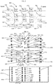
- FIG. 4 shows the connections between the two switching dies 152 and 154 and the switching interface region 170 in FIG. 1B in order to implement part of the switching network circuit 300 in FIG. 3 in the three dimensional cross point switching unit 150.
- the programmable component area 142 includes the switching interface region 170 having cross connections such as the TSVs 260, 262, 270, 272, and 274 in FIGs. 2A and 2B , which allow routing to and from the stacked switching dies 152 and 154.
- the switching dies 152 and 154 are configured to implement a cross bar switching circuit such as the configuration of the cross bar circuit 300 in FIG. 3 .
- the switching die 152 includes the two 2 x 2 cross bar ingress switches 202 and 204, which correspond with the switches 302 (X11) and 304 (X12) in FIG. 3 .
- the switching die 152 also includes the two other middle stage 2 x 2 switches 220 and 222 corresponding to the switches 312 (X21) and 314 (X22) in FIG. 3 .
- the interconnections at the chip level of the switching die 152 between the ingress switches 202 and 204 and the middle stage switches 220 and 232 are controlled by the multiplexers 206, 208, 210, and 212.
- the switching die 154 includes the two 2 x 2 switches 232 and 234, which correspond with the switches 306 (X13) and 308 (X14) in FIG. 3 .
- the switching die 154 also includes the two other middle stage 2 x 2 switches 250 and 252 corresponding to the switches 316 (X23) and 318 (X24) in FIG. 3 .
- the interconnections at the chip level of the switching die 154 between the ingress switches 232 and 234 and the middle stage switches 250 and 252 are controlled by the multiplexers 236, 238, 240 and 242.
- the multiplexers 206, 208, 210 and 212 in conjunction with TSVs 260, 262, 270, 272, and 274 in FIG.
- the multiplexers in conjunction with the TSVs 260, 262, 270, 272, and 274 also allow the routing of connections from the switching interface region 170 on the component die 100 to switching dies above the switching die 154 such as the switching die 156 or the switching die 152 below the switching die 154.
- a first set of TSVs 400 on the switching interface region 170 provide connections to the four inputs of the ingress switches 202 and 204 on the first switching die 152.
- a second set of TSVs 402 provide connections to the four inputs of the ingress switches 232 and 234 on the second switching die 154.
- the switching interface region 170 in this example thus has up to eight ports, which are coupled to the TSVs 400 and 402 to provide inputs to the switching dies 152 and 154.
- Other TSVs may be used for additional ports if additional switching dies such as the switching die 156 are stacked on the switching die 154.
- a set of output TSVs 406 are coupled from the outputs of the middle stage switches such as the switches 210 and 212 to output ports on the switching interface region 170. It is to be understood that the outputs from the middle stage switches may be coupled to additional stages of switches on the switching dies 152, 154, 156, and 158 if additional switching flexibility and capability is desired.
- the ingress switch 202 on the switching die 152 has two outputs 410 and 412.
- the first output 410 is coupled to one of the inputs of the multiplexer 236, which may then be routed to the input of the middle stage switch 220 as per the layout of the switching unit 300 in FIG. 3 .
- the first output 410 is also coupled to a TSV 414, which leads to an output port of the switching interface region 170 of the programmable component area 142 on the component die of the programmable logic device 100.
- the second output 412 is coupled to an input of the multiplexer 210, which may then be routed to the input of the middle stage switch 222.
- the second output 412 of the switch 202 is also coupled to a TSV 416, which leads to an output port of the switching interface region 170 of the programmable component area 142 on the component die.
- the second output 412 of the switch 202 is also coupled to a TSV 428, which is coupled to an input of the multiplexer 236 of the switching die 154 following the layout of FIG. 3 .
- the ingress switch 204 has two outputs 420 and 422.
- the first output 420 is coupled to one of the inputs of the multiplexer 208, which may then be routed to the input of the middle stage switch 220 as per the layout of the switching unit 300 in FIG. 3 .
- the first output 420 is also coupled to a TSV 424, which leads to the switching interface region 170 of the programmable component area 142.
- the second output 422 is coupled to an input of the multiplexer 212, which may then be routed to the input of the middle stage switch 222.
- the second output 422 is also coupled to a TSV 426, which leads to an output port of the switching interface region 170 of the programmable component area 142.
- the second output 422 is also coupled to a TSV 430, which is coupled to an input of the multiplexer 238 of the switching die 154 following the layout of FIG. 3 .
- the multiplexer 206 may select between two separate inputs, which may be connected to one of the inputs of the middle stage switch 220.
- the first input is the output 410 of the switch 202, which follows the layout of FIG. 3 .
- the second input is a TSV 432 from the switching interface region 170 of the programmable component area 142, which allows bypassing the switch 202 and direct access to the inputs of the middle stage switch 220.
- the multiplexer 208 may select between two separate inputs, which may be connected to the middle stage switch 222.
- the first input is the output 422 from the switch 204, which follows the layout in FIG. 3 .
- the second input is a TSV 434 from the switching interface region 170 of the programmable component area 142, which allows bypassing the switch 202 and directly accessing the inputs of the middle stage switch 220.
- two TSVs 436 and 438 from the switching interface region 170 of the programmable component area 142 are connected to the multiplexers 210 and 212, respectively, to bypass the switch 204 and directly access the inputs of the middle stage switch 222.
- the multiplexer 210 may select between three inputs.
- the first input is the second output 412 of the switch 202.
- the second input is the TSV 436 from the switching interface region 170 of the programmable component area 142 to bypass the switch 204 and directly access the inputs of the middle stage switch 222.
- the third input of the multiplexer 210 is the first output of the switch 232 on the switching die 154, which is routed via a TSV 440 and follows the configuration of FIG. 3 .
- the multiplexer 212 may select between three inputs.
- the first input is the second output 422 of the switch 204.
- the second input is the TSV 438 from the programmable component area 142 to bypass the switch 204 and directly access the inputs of the middle stage switch 222.
- the third input of the multiplexer 212 is the output of the switch 234 of the switching die 154, which is routed by a TSV 442 and follows the configuration of FIG. 3 .
- the switching die 154 is stacked on the switching die 152.
- the inputs of the switches 232 and 234 are coupled to the switching interface region 170 of the programmable component area 142 via TSVs 402.
- the outputs of the switches 232 and 234 are coupled to TSVs 450, 452, 454, and 456 to provide the outputs to the switching interface region 170 of the programmable component area 142.
- Two TSVs 460 and 462 from the switching interface region 170 of the programmable component area 142 are connected to the multiplexers 236 and 238, respectively, to bypass the switch 232 and directly access the inputs of the switch 250.
- Two TSVs 464 and 466 from the switching interface region 170 of the programmable component area 142 are connected to the multiplexers 240 and 242, respectively, to bypass the switch 234 and directly access the inputs of the switch 252.
- the outputs of the switches 232 and 234 are connected to inputs of the multiplexers 236, 238, 240, and 242 to allow routing to the inputs of the switches 250 and 252 respectively.
- the multiplexer 236 includes three inputs, which may be selected, one of which is coupled to the output of the switch 232.
- the second input is an input routed from the TSV 460 from the switching interface region 170 of the programmable component area 142.
- the third input is the output of the switch 204 of the switching die 152 from the TSV 428 following the layout in FIG. 3 .
- the multiplexer 238 has three inputs, which may be selected. The first input is coupled to the output of the switch 234.
- the second input is routed from the TSV 462 from switching interface region 170 of the programmable component area 142.
- the third input is the output 422 of the switch 204 of the switching die 152 that is routed via the TSV 430, following the configuration in FIG. 3 .
- the multiplexer 240 has two inputs, which may be selected. The first input is one of the outputs of the switch 232 following the configuration of FIG. 3 . The second input is an input from the switching interface region 170, which is routed via the TSV 464. Similarly, the multiplexer 242 also has two inputs, which may be selected. The first input is one of the outputs of the switch 234 following the configuration in FIG. 3 . The second input is an input from the switching interface region 170, which is routed via the TSV 466.
- the cross point switch layout in FIG. 3 is split in implementation between the programmable component die including the switching interface region 170 and the hardened logic switching dies 152, 154, 156, and 158.
- the stacked switching dies such as the switching dies 152, 154, 156, and 158 allow the implementation of a cross connect switch, which is scalable by adding additional switching dies and corresponding cross connects between the switching dies and the switching interface region 170 of the programmable component area 142.
- the network of switches may be accomplished by duplicating the existing switching die structure and adding additional switching dies on the top of the existing switching dies.
- the switching die 152 in combination with the switching interface region 170, allows a 4 x 4 cross point switch, which may be configured using the control circuit 180 controlling the outputs of the multiplexers 206, 208, 210, and 212.
- a cross point switch may be essentially hardwired by maintaining the control signals to the multiplexers 206, 208, 210, and 212 to the desired routing between the switches 202, 204, 220, and 222 and the switching interface region 170.
- the resulting cross-point switch may also be configurable by changing the control signals to multiplexers 206, 208, 210, and 212 to allow combination of inputs from the switching interface region 170.
- Expanding this network to twice the port count may be accomplished by duplicating the existing network, and adding a new column to the left and the right in FIG. 3 .
- the second switching die 154 may be added on top of the first switching die 152.
- the top entry switches 202 and 204 is connected to the top port of the top matrix (switch 220) and the top port of the bottom matrix (switch 250).
- This pattern continues (one top, one bottom connection) for the ingress and egress switches in FIG. 3 .
- the added column to the right to the output switches is a mirror of the interconnect pattern of the middle stage switches in FIG. 3 .
- the desired cross-point switch may be scaled by adding 4 more inputs in the form of the second switching die 154.
- the result is an 8 x 8 cross point switch, which may be configured using the control circuit 180 controlling the outputs of the multiplexers 206, 208, 210, and 212 on the first switching die 152 and the multiplexers 236, 238, 240, and 242 on the second switching die 154.
- the cross-point switch may either be hardwired where the control signals are maintained to the multiplexers or may be configurable by changing the control signals depending on the desired connections between switches.
- This process allows port scaling to be done in the three dimensional stacked die environment of the cross-point switching unit 150 by building a fixed-size cross point switch with the switching dies 152 and 154 but adding die to die interconnection and on chip muxing for both dies as shown in FIG. 2A-2B .
- the entire cross point switch would not need to be implemented on hard logic on the switching dies 152, 154, 156, and 158.
- the first stage or last stages of switching could be implemented in soft logic that also has access to the TSV interconnect structure to use other hard switching dies.
- the ingress switches on the switching dies 152 and 154 in FIG. 4 could be implemented via programmable hardware instead of in hard logic.
- the switching die implementing a switch may be constructed to be late-binding programmable.
- the switch can be programmed to implement a blocking network at significantly lower cost than a Benes-network as previously described.
- Another process may be the transportation of a switch program via a TSV to the multiplexers on the switching dies from an FPGA circuit such as one of the programmable regions 140 in FIG. 1 configured to execute a switch configuration program.
- the hard wired switching dies implementing the three dimensional crossbar switching unit 150 serve purposes that are separable from the core functionality of a programmable circuit or a fixed function processing circuit. These include the physical coding sublayer (PCS) and crossbar function for lane re-ordering and striping.
- PCS physical coding sublayer
- crossbar function for lane re-ordering and striping.
- the specific implementation in FIG. 3 may be used for a soft-Ethernet core for PCS virtual lane re-ordering.
- the programming of the switches on the switching dies 152 and 154 via the multiplexers is pseudo-static and determined at boot-time by a simple processor such as the processor 160, which allows for the appropriate programming of the switches.
- FIG. 5 is a diagram of a wireless communications system 500 using the example cross point switching unit.
- the wireless communication system 500 has a series of cell phone towers such as a cell phone tower 510.
- the cell phone tower 510 includes multiple antennas 512, 514, 516, and 518.
- Each of the antennas 512, 514, 516, and 518 must be separately powered up and powered down.
- the antennas 512, 514, 516, and 518 are selectively powered up to receive and transmit network traffic.
- Each powered antenna adds additional capability to handle a corresponding increase in network traffic volume.
- the antennas 512, 514, 516, and 518 are powered up to meet the requirements of peak network traffic.
- non-peak times such as late at night, only one of the antennas such as the antenna 512 is powered up as the network traffic is at a lower volume.
- the system 500 includes a baseband processing unit 520, which is coupled to the antennas 512, 514, 516, and 518 via an interface 522, which includes a series of cables 532.
- the antennas 512, 514, 516, and 518 communicate with the baseband processing unit 520 via a CPRI communications standard operated by the interface 522.
- the baseband processing unit 520 includes a programmable circuit such as the programmable logic device 100 in FIG. 1A .
- the baseband processing unit 520 includes a scalable cross point switching unit 530, which is similar to the cross point switching unit 150 in FIGs. 1-4 .
- the inputs of the cross point switching unit 150 are the series of cables 532 of the interface 522, which each carry CPRI signals from one of the antennas 512, 514, 516, and 518.
- the signals are routed through the cross point switching unit 150 to different output ports 534 and 536.
- the output ports 534 and 536 are coupled to processing logic units 540.
- Each of the processing logic units 540 process the signals and output corresponding media through output ports.
- the baseband processing unit 520 includes a data port 542 for data signals and a SONET port 544 for voice data.
- the output ports 542 and 544 are coupled to different networks such as a data network and a phone network, respectively.
- the three-dimensional cross point switching unit 530 allows the various processing blocks of the processing logic 540 to be effectively turned off by switching the outputs of active antennas to selected processing blocks.
- Using the cross point switching unit 530 eliminates the various cases of port activity.
- certain output ports are inactive such as the ports 534 when some of the antennas are not powered.
- the active ports such as the ports 536 are coupled via the cross point switching unit 530 to the active antennas.
- the cross point switch 530 Rather than needing to verify that a first processing logic block and a second processing logic block or antenna 512 (PL1) and antenna 516 (PL3) or antenna 512 (PL1) and antenna 518 (PL4) all need to work together correctly, the cross point switch 530 allows the system designer to only need to verify that antenna 512 or antenna 512 and antenna 514 or antennas 512, 514 and 516 or antennas 512, 514, 516 and 518 all work together correctly. Since the processing logic is complex, the simplification that the cross point switching unit 530 allows is considerable and allows faster time to market for suppliers who use this structure.
- Interlaken is an interface that is a channelized interface that can be mapped to a mix of different port speeds. This interface is frequently used in data communications carrier equipment to have channels communicate with a packet processing block. In practice, Interlaken allows different customers to purchase different ports for scaling desired bandwidth.
- an Interlaken interconnect may be implemented by configuring the switching unit 150 to provide bundles of serial links to create a logical connection between components with multiple channels, backpressure capability, and data-integrity protection as per the Interlaken protocol.
- Each of the processing blocks 720 are coupled to outputs 728 from a three-dimensional cross point switching unit 730.
- the allocation of the Interlaken ports 702a-e to the processing logic is determined by a customer forwarding table 732.
- the Interlaken input ports 702a-e are coupled to the scalable cross point switching unit 730, which is similar to the cross point switching unit 150 in FIGs. 1-4 .
- the Interlaken input ports 702a-f are routed via the cross point switching unit 730 to the processing logic blocks 720, which are associated with different customers.
- a carrier has customer 1 and 2 both purchasing two input ports of bandwidth.
- the carrier may assign customer 1 to ports 1 and 2 (702a and 702b), and customer 2 to ports 3 and 4 (702c and 702d) to keep customer processing efficient.
- customer 1 wants to purchase additional port bandwidth
- additional input ports may be assigned to the processing block associated with customer 1.
- customer 1 may be assigned port 5 (702e), which allows customer 1 to receive network traffic from ports 1, 2, and 5. This is done so that customer 2 is not affected by customer 1 purchasing additional service.
- the carrier In order to process the traffic correctly, the carrier must move port 5 next to ports 1 and 2 so they can all use the same database for deciding where packets need to go.
- switching the ports as in current practice such as moving port 3 to customer 1 and moving port 5 to customer 2 causes service interruptions.
- the switching unit 730 allows the ports to be moved virtually to the associated customer thus avoiding service interruptions.
- the port 702e (port 5) is simply routed by the cross point switching unit 730 to the processing logic 726 associated with customer 1 without interrupting the data flow of the ports assigned to customer 2. This change may be accomplished by changing the customer forwarding table 732 without interrupting service to customer 2.
Landscapes
- Engineering & Computer Science (AREA)
- Physics & Mathematics (AREA)
- Computer Hardware Design (AREA)
- General Engineering & Computer Science (AREA)
- Theoretical Computer Science (AREA)
- Mathematical Physics (AREA)
- General Physics & Mathematics (AREA)
- Computing Systems (AREA)
- Computer Networks & Wireless Communication (AREA)
- Software Systems (AREA)
- Logic Circuits (AREA)
- Design And Manufacture Of Integrated Circuits (AREA)
Claims (15)
- Konfigurierbares Crosspoint-Umschaltsystem, das Folgendes umfasst:einen Komponentenchip (100), der Logikkomponenten und einen Umschaltschnittstellenbereich (170), um eine Verbindung der Logikkomponenten zu ermöglichen, enthält;gekennzeichnet durcheinen ersten Umschaltchip (152), der sich am Komponentenchip befindet, wobei der erste Umschaltchip einen Eingangsstufenschalter (202, 204), der einen Eingang und einen Ausgang besitzt, und einen Mittelstufenschalter (220, 222), der einen Eingang besitzt, enthält;einen Multiplexer (206, 208, 210, 212), der einen Eingang, der an den Ausgang des Eingangsstufenschalters gekoppelt ist, und einen Ausgang, der an den Eingang des Mittelstufenschalters gekoppelt ist, besitzt;eine Eingangsdurchkontaktierung durch Silicium, TSV (260, 400, 402), die zwischen einen Eingangsanschluss im Umschaltschnittstellenbereich und den Eingang des Eingangsstufenschalters gekoppelt ist; undeine zweite Eingangs-TSV (270, 432, 434, 436, 438, 460, 462, 464, 466), die zwischen einen zweiten Eingangsanschluss im Umschaltschnittstellenbereich des Komponentenchips und einen weiteren Eingang des Multiplexers gekoppelt ist.
- Umschaltsystem nach Anspruch 1, wobei das Umschaltsystem konfiguriert ist, eine Verbindung von den Eingängen des Multiplexers zum Mittelstufenumschalter auszuwählen.
- Umschaltsystem nach Anspruch 1, wobei sich der Multiplexer am ersten Umschaltchip befindet.
- Umschaltsystem nach Anspruch 1, wobei der Eingangsstufenschalter, der Mittelstufenschalter und der Multiplexer feste Schaltungsanordnungen sind.
- Umschaltsystem nach Anspruch 1, wobei der Komponentenchip eine programmierbare Logik (140) enthält, um zwischen dem ersten und dem zweiten Eingangsanschluss auszuwählen.
- Umschaltsystem nach Anspruch 5, wobei die Konfiguration des Umschaltschnittstellenbereichs in einer FPGA-Logik des Komponentenchips erzeugt wird, wobei die Konfigurationsdaten über Verbindungen zum Multiplexer gesendet werden.
- Umschaltsystem nach Anspruch 1, das ferner einen Prozessor umfasst, um die Verbindungen zum Eingang des Mittelschalters über den Multiplexer zu programmieren.
- Umschaltsystem nach Anspruch 1, das ferner Folgendes umfasst:eine erste Ausgangs-TSV (262), die den Ausgang des Eingangsstufenschalters an einen ersten Ausgangsanschluss im Umschaltschnittstellenbereich koppelt; undeine zweite Ausgangs-TSV (276), die den Ausgang des Mittelstufenschalters an einen zweiten Ausgangsanschluss im Umschaltschnittstellenbereich koppelt.
- Umschaltsystem nach Anspruch 3, das ferner Folgendes umfasst:einen zweiten Umschaltchip (154), der auf den ersten Umschaltchip gestapelt ist, wobei der zweite Umschaltchip einen Eingangsstufenschalter (232, 234) mit einem Eingang und einem Ausgang, der an einen Eingang eines Multiplexers (236, 238, 240, 242) gekoppelt ist, und einen Mittelstufenschalter (250, 252), der an den Ausgang des Multiplexers gekoppelt ist, enthält; undeine Eingangs-TSV, die zwischen einen Anschluss im Umschaltschnittstellenbereich und den Eingang des Eingangsstufenschalters (232, 234) gekoppelt ist;eine erste Umschaltchip-Eingangs-TSV (428), die zwischen den Ausgang des Eingangsstufenschalters (202, 204) des ersten Umschaltchips und einen weiteren Eingang des Multiplexers (236, 238, 240, 242) des zweiten Umschaltchips gekoppelt ist, wobei das Umschaltsystem konfiguriert ist, eine Verbindung zum Mittelstufenschalter (250, 252) des zweiten Umschaltchips über die Eingänge des Multiplexers des zweiten Umschaltchips auszuwählen; undeine zweite Umschaltchip-Eingangs-TSV (440), die zwischen den Ausgang des Eingangsstufenschalters (232, 234) des zweiten Umschaltchips und einen weiteren Eingang des Multiplexers (206, 208, 210, 212) des ersten Umschaltchips gekoppelt ist.
- Umschaltsystem nach Anspruch 9, wobei die Multiplexer des ersten und des zweiten Umschaltchips konfiguriert sind, eine vorgegebene Anzahl von Eingangsanschlüssen am Umschaltschnittstellenbereich als Umschalteingänge und eine vorgegebene Anzahl von Ausgangsanschlüssen an den Umschaltschnittstellenbereichen als Umschaltausgänge auszuwählen.
- Umschaltsystem nach Anspruch 10, wobei das Umschaltsystem konfiguriert ist, über die Multiplexer des ersten und des zweiten Umschaltchips einen breiten Kanalwortbreitenanschluss durch Zuweisen mehrerer Eingänge von Ausgangsschaltern des ersten und des zweiten Umschaltchips zu einem einzelnen Eingangsanschluss zu erstellen.
- Umschaltsystem nach Anspruch 9, wobei das Umschaltsystem über die Multiplexer des ersten und des zweiten Umschaltchips konfiguriert ist, dem Ethernet-Bitübertragungsunterschichtprotokoll zu entsprechen.
- Umschaltsystem nach Anspruch 9, wobei das Umschaltsystem über die Multiplexer des ersten und des zweiten Umschaltchips konfiguriert ist, Eingänge gemäß dem Interlaken-Schnittstellenprotokoll aufzunehmen.
- Verfahren zum Konfigurieren eines Crosspoint-Umschalters für Querverbindungen von Komponenten an einem Komponentenchip (100), wobei das Verfahren Folgendes umfasst:Hinzufügen eines ersten Umschaltchips (152) über den Komponentenchip, wobei der erste Umschaltchip mehrere Eingangsstufenschalter (202, 204), die mit den Multiplexern (206, 208, 210, 212), die Ausgänge, die an die Eingänge von mehreren Mittelstufenschaltern (220, 222) gekoppelt sind, besitzen, querverbunden sind, enthält;Koppeln einer Eingangsdurchkontaktierung durch Silicium, TSV (260, 400, 402) zwischen einen Eingangsanschluss und die Eingänge der Eingangsstufenschalter des ersten Umschaltchips; undSteuern (180) des Multiplexers, die Eingänge aus dem Eingangsanschluss oder den Ausgängen des Eingangsstufenschalters für den Mittelstufenschalter auszuwählen.
- Konfigurierbare Crosspoint-Umschalteinheit, die Folgendes umfasst:einen Komponentenchip (100), der einen Verbindungsschnittstellenbereich (170), der Eingangsanschlüsse und Ausgangsanschlüsse enthält, enthält;gekennzeichnet durchmehrere Umschaltchips (152, 154), die auf den Komponentenchip gestapelt sind, wobei jeder der mehreren Umschaltchips mehrere Eingangsschalter (202, 204, 232, 234), mehrere Multiplexer (206, 208, 210, 212, 236, 238, 240, 242) und mehrere Mittelstufenschalter (220, 222, 250, 252) enthält, wobei die Ausgänge der Eingangsschalter über die Multiplexer mit den Eingängen der Mittelstufenschalter für jeden der mehreren Umschaltchips verbunden sind;mehrere Eingangsdurchkontaktierungen durch Silicium, TSV (260, 400, 402), zwischen den Eingangsanschlüssen des Verbindungsschnittstellenbereichs und den Eingängen der Eingangsschalter der mehreren Umschaltchips; undmehrere Ausgangs-TSVs (262, 276) zwischen den Ausgangsanschlüssen des Verbindungsschnittstellenbereichs und den Ausgängen der Eingangsschalter und den Mittelstufenschaltern; wobeimindestens einer der Umschaltchips eine erste Mehrzahl von TSVs zwischen den Ausgängen der Eingangsschalter und dem Multiplexer von einem Umschaltchip auf dem mindestens einen der Umschaltchips und eine zweite Mehrzahl von TSVs zwischen den Ausgängen der Eingangsschalter und dem Multiplexer eines Umschaltchips unter dem mindestens einen der Umschaltchips enthält.
Applications Claiming Priority (1)
| Application Number | Priority Date | Filing Date | Title |
|---|---|---|---|
| US14/282,510 US9077338B1 (en) | 2014-05-20 | 2014-05-20 | Method and circuit for scalable cross point switching using 3-D die stacking |
Publications (2)
| Publication Number | Publication Date |
|---|---|
| EP2947893A1 EP2947893A1 (de) | 2015-11-25 |
| EP2947893B1 true EP2947893B1 (de) | 2018-10-10 |
Family
ID=53283995
Family Applications (1)
| Application Number | Title | Priority Date | Filing Date |
|---|---|---|---|
| EP15168439.6A Active EP2947893B1 (de) | 2014-05-20 | 2015-05-20 | Verfahren und schaltung zur skalierbaren kreuzungspunktschaltung mittels 3d-chipstapelung |
Country Status (3)
| Country | Link |
|---|---|
| US (2) | US9077338B1 (de) |
| EP (1) | EP2947893B1 (de) |
| CN (1) | CN105099423B (de) |
Families Citing this family (14)
| Publication number | Priority date | Publication date | Assignee | Title |
|---|---|---|---|---|
| EP3480956B1 (de) * | 2013-03-15 | 2021-01-06 | The Regents of the University of California | Netzwerkarchitekturen für grenzenlose hierarchische verbindungen |
| US9077338B1 (en) * | 2014-05-20 | 2015-07-07 | Altera Corporation | Method and circuit for scalable cross point switching using 3-D die stacking |
| EP3308349B1 (de) | 2015-06-10 | 2025-01-29 | Mobileye Vision Technologies Ltd. | Bildprozessor und verfahren zur verarbeitung eines bildes |
| US11178072B2 (en) | 2015-06-10 | 2021-11-16 | Mobileye Vision Technologies Ltd. | Image processor and methods for processing an image |
| US9898375B1 (en) | 2015-12-22 | 2018-02-20 | EMC IP Holding Company LLC | Asymmetric memory transceiver |
| US10235314B2 (en) * | 2015-12-28 | 2019-03-19 | EMC IP Holding Company LLC | Fabric for modular solid-state storage systems |
| US9929979B2 (en) | 2016-01-07 | 2018-03-27 | Analog Devices, Inc. | Scalable crosspoint switch |
| CN106712751A (zh) * | 2016-11-25 | 2017-05-24 | 深圳市紫光同创电子有限公司 | 互联装置、现场可编程门阵列器件及其信号传输控制方法 |
| US10333508B2 (en) | 2017-03-29 | 2019-06-25 | International Business Machines Corporation | Cross bar switch structure for highly congested environments |
| US10169511B2 (en) | 2017-03-29 | 2019-01-01 | International Business Machines Corporation | Method to synthesize a cross bar switch in a highly congested environment |
| WO2019116106A2 (en) * | 2017-12-14 | 2019-06-20 | Mobileye Vision Technologies Ltd. | Image processor and methods for processing an image |
| US11146505B2 (en) * | 2018-01-11 | 2021-10-12 | Intel Corporation | Low latency compact Clos network controller |
| US10666261B2 (en) * | 2018-12-28 | 2020-05-26 | Intel Corporation | High-speed core interconnect for multi-die programmable logic devices |
| CN120111876B (zh) * | 2023-12-06 | 2026-01-06 | 长鑫科技集团股份有限公司 | 一种存储芯片、逻辑芯片、芯片堆叠结构和存储器 |
Family Cites Families (14)
| Publication number | Priority date | Publication date | Assignee | Title |
|---|---|---|---|---|
| US6181159B1 (en) * | 1997-05-06 | 2001-01-30 | Altera Corporation | Integrated circuit incorporating a programmable cross-bar switch |
| US6721311B1 (en) * | 1999-08-10 | 2004-04-13 | Colorado Seminary | Self-routing permutation networks based on de Bruijn digraphs |
| US7256611B2 (en) * | 2000-05-31 | 2007-08-14 | Silicon Laboratories Inc. | Cross-bar matrix with LCD functionality |
| US7177301B2 (en) * | 2001-12-27 | 2007-02-13 | Intel Corporation | Signal permuting |
| US7057412B1 (en) * | 2003-12-12 | 2006-06-06 | Altera Corporation | Configurable crossbar switch |
| KR100812225B1 (ko) * | 2005-12-07 | 2008-03-13 | 한국전자통신연구원 | 멀티프로세서 SoC 플랫폼에 적합한 크로스바 스위치구조 |
| US8373440B2 (en) * | 2009-04-06 | 2013-02-12 | Hewlett-Packard Development Company, L.P. | Three dimensional multilayer circuit |
| US8786080B2 (en) * | 2011-03-11 | 2014-07-22 | Altera Corporation | Systems including an I/O stack and methods for fabricating such systems |
| US8548071B2 (en) * | 2011-07-19 | 2013-10-01 | Xilinx, Inc. | Integrated circuit enabling the communication of data and a method of communicating data in an integrated circuit |
| US8542032B1 (en) * | 2012-01-06 | 2013-09-24 | Altera Corporation | Integrated circuits with interconnect selection circuitry |
| US8519740B2 (en) * | 2012-01-06 | 2013-08-27 | Altera Corporation | Integrated circuits with shared interconnect buses |
| US9268738B2 (en) * | 2012-02-24 | 2016-02-23 | International Business Machines Corporation | Three-dimensional permute unit for a single-instruction multiple-data processor |
| US9165968B2 (en) * | 2012-09-14 | 2015-10-20 | Taiwan Semiconductor Manufacturing Co., Ltd. | 3D-stacked backside illuminated image sensor and method of making the same |
| US9077338B1 (en) * | 2014-05-20 | 2015-07-07 | Altera Corporation | Method and circuit for scalable cross point switching using 3-D die stacking |
-
2014
- 2014-05-20 US US14/282,510 patent/US9077338B1/en active Active
-
2015
- 2015-05-20 EP EP15168439.6A patent/EP2947893B1/de active Active
- 2015-05-20 CN CN201510259562.2A patent/CN105099423B/zh active Active
- 2015-07-06 US US14/791,917 patent/US9276582B2/en active Active
Non-Patent Citations (1)
| Title |
|---|
| None * |
Also Published As
| Publication number | Publication date |
|---|---|
| US9276582B2 (en) | 2016-03-01 |
| US9077338B1 (en) | 2015-07-07 |
| EP2947893A1 (de) | 2015-11-25 |
| CN105099423B (zh) | 2019-01-01 |
| US20150341037A1 (en) | 2015-11-26 |
| CN105099423A (zh) | 2015-11-25 |
Similar Documents
| Publication | Publication Date | Title |
|---|---|---|
| US9077338B1 (en) | Method and circuit for scalable cross point switching using 3-D die stacking | |
| US6590417B1 (en) | Cascadable bus based crossbar switch in a programmable logic device | |
| Chan et al. | Architectural tradeoffs in field-programmable-device-based computing systems | |
| EP3047655B1 (de) | Systeme und verfahren für mems-basierte elektrische kreuzpunktumschaltung | |
| USRE50417E1 (en) | VLSI layouts of fully connected generalized networks | |
| US8270400B2 (en) | Fully connected generalized multi-stage networks | |
| US20120124257A1 (en) | Multichip module for communications | |
| US8363649B2 (en) | Fully connected generalized multi-link multi-stage networks | |
| US8493090B1 (en) | Multiplexer-based interconnection network | |
| US10313047B2 (en) | Optical wavelength selective switch, an optical network node, an optical network and methods therein | |
| US20180212899A1 (en) | Fast scheduling and optmization of multi-stage hierarchical networks | |
| US20160261525A1 (en) | Optimization of multi-stage hierarchical networks for practical routing applications | |
| US9374322B2 (en) | Optimization of multi-stage hierarchical networks for practical routing applications | |
| US6605959B1 (en) | Structure and method for implementing wide multiplexers | |
| US20170099052A1 (en) | Local routing network with selective fast paths for programmable logic device | |
| CN113270124A (zh) | 可编程半导体器件组织成多个时钟区域的方法和装置 | |
| Quinton et al. | Concentrator access networks for programmable logic cores on SoCs | |
| KR20230169096A (ko) | 고대역폭 인터페이스를 위한 로컬화된 noc 스위칭 인터커넥트 | |
| JP2017513404A (ja) | フィールドプログラマブルゲートアレイ及び通信方法 | |
| CN107733816B (zh) | 一种新型的严格无阻塞交换网络 | |
| CN101517546B (zh) | 一种用于逻辑阵列的可编程互连网络 | |
| Chiricescu et al. | A three-dimensional FPGA with an integrated memory for in-application reconfiguration data | |
| US7197032B1 (en) | Switch architecture using multiple crossbars | |
| US11777872B1 (en) | Optimization of multi-stage hierarchical networks for practical routing applications | |
| US7999570B2 (en) | Enhanced permutable switching network with multicasting signals for interconnection fabric |
Legal Events
| Date | Code | Title | Description |
|---|---|---|---|
| PUAI | Public reference made under article 153(3) epc to a published international application that has entered the european phase |
Free format text: ORIGINAL CODE: 0009012 |
|
| 17P | Request for examination filed |
Effective date: 20150520 |
|
| AK | Designated contracting states |
Kind code of ref document: A1 Designated state(s): AL AT BE BG CH CY CZ DE DK EE ES FI FR GB GR HR HU IE IS IT LI LT LU LV MC MK MT NL NO PL PT RO RS SE SI SK SM TR |
|
| AX | Request for extension of the european patent |
Extension state: BA ME |
|
| RBV | Designated contracting states (corrected) |
Designated state(s): AL AT BE BG CH CY CZ DE DK EE ES FI FR GB GR HR HU IE IS IT LI LT LU LV MC MK MT NL NO PL PT RO RS SE SI SK SM TR |
|
| GRAP | Despatch of communication of intention to grant a patent |
Free format text: ORIGINAL CODE: EPIDOSNIGR1 |
|
| STAA | Information on the status of an ep patent application or granted ep patent |
Free format text: STATUS: GRANT OF PATENT IS INTENDED |
|
| INTG | Intention to grant announced |
Effective date: 20180530 |
|
| GRAS | Grant fee paid |
Free format text: ORIGINAL CODE: EPIDOSNIGR3 |
|
| GRAA | (expected) grant |
Free format text: ORIGINAL CODE: 0009210 |
|
| STAA | Information on the status of an ep patent application or granted ep patent |
Free format text: STATUS: THE PATENT HAS BEEN GRANTED |
|
| AK | Designated contracting states |
Kind code of ref document: B1 Designated state(s): AL AT BE BG CH CY CZ DE DK EE ES FI FR GB GR HR HU IE IS IT LI LT LU LV MC MK MT NL NO PL PT RO RS SE SI SK SM TR |
|
| REG | Reference to a national code |
Ref country code: GB Ref legal event code: FG4D |
|
| REG | Reference to a national code |
Ref country code: CH Ref legal event code: EP Ref country code: AT Ref legal event code: REF Ref document number: 1052673 Country of ref document: AT Kind code of ref document: T Effective date: 20181015 |
|
| REG | Reference to a national code |
Ref country code: IE Ref legal event code: FG4D |
|
| REG | Reference to a national code |
Ref country code: DE Ref legal event code: R096 Ref document number: 602015017721 Country of ref document: DE |
|
| REG | Reference to a national code |
Ref country code: NL Ref legal event code: FP |
|
| REG | Reference to a national code |
Ref country code: LT Ref legal event code: MG4D |
|
| REG | Reference to a national code |
Ref country code: AT Ref legal event code: MK05 Ref document number: 1052673 Country of ref document: AT Kind code of ref document: T Effective date: 20181010 |
|
| PG25 | Lapsed in a contracting state [announced via postgrant information from national office to epo] |
Ref country code: ES Free format text: LAPSE BECAUSE OF FAILURE TO SUBMIT A TRANSLATION OF THE DESCRIPTION OR TO PAY THE FEE WITHIN THE PRESCRIBED TIME-LIMIT Effective date: 20181010 Ref country code: LV Free format text: LAPSE BECAUSE OF FAILURE TO SUBMIT A TRANSLATION OF THE DESCRIPTION OR TO PAY THE FEE WITHIN THE PRESCRIBED TIME-LIMIT Effective date: 20181010 Ref country code: FI Free format text: LAPSE BECAUSE OF FAILURE TO SUBMIT A TRANSLATION OF THE DESCRIPTION OR TO PAY THE FEE WITHIN THE PRESCRIBED TIME-LIMIT Effective date: 20181010 Ref country code: BG Free format text: LAPSE BECAUSE OF FAILURE TO SUBMIT A TRANSLATION OF THE DESCRIPTION OR TO PAY THE FEE WITHIN THE PRESCRIBED TIME-LIMIT Effective date: 20190110 Ref country code: PL Free format text: LAPSE BECAUSE OF FAILURE TO SUBMIT A TRANSLATION OF THE DESCRIPTION OR TO PAY THE FEE WITHIN THE PRESCRIBED TIME-LIMIT Effective date: 20181010 Ref country code: HR Free format text: LAPSE BECAUSE OF FAILURE TO SUBMIT A TRANSLATION OF THE DESCRIPTION OR TO PAY THE FEE WITHIN THE PRESCRIBED TIME-LIMIT Effective date: 20181010 Ref country code: AT Free format text: LAPSE BECAUSE OF FAILURE TO SUBMIT A TRANSLATION OF THE DESCRIPTION OR TO PAY THE FEE WITHIN THE PRESCRIBED TIME-LIMIT Effective date: 20181010 Ref country code: LT Free format text: LAPSE BECAUSE OF FAILURE TO SUBMIT A TRANSLATION OF THE DESCRIPTION OR TO PAY THE FEE WITHIN THE PRESCRIBED TIME-LIMIT Effective date: 20181010 Ref country code: IS Free format text: LAPSE BECAUSE OF FAILURE TO SUBMIT A TRANSLATION OF THE DESCRIPTION OR TO PAY THE FEE WITHIN THE PRESCRIBED TIME-LIMIT Effective date: 20190210 Ref country code: NO Free format text: LAPSE BECAUSE OF FAILURE TO SUBMIT A TRANSLATION OF THE DESCRIPTION OR TO PAY THE FEE WITHIN THE PRESCRIBED TIME-LIMIT Effective date: 20190110 |
|
| PG25 | Lapsed in a contracting state [announced via postgrant information from national office to epo] |
Ref country code: SE Free format text: LAPSE BECAUSE OF FAILURE TO SUBMIT A TRANSLATION OF THE DESCRIPTION OR TO PAY THE FEE WITHIN THE PRESCRIBED TIME-LIMIT Effective date: 20181010 Ref country code: RS Free format text: LAPSE BECAUSE OF FAILURE TO SUBMIT A TRANSLATION OF THE DESCRIPTION OR TO PAY THE FEE WITHIN THE PRESCRIBED TIME-LIMIT Effective date: 20181010 Ref country code: GR Free format text: LAPSE BECAUSE OF FAILURE TO SUBMIT A TRANSLATION OF THE DESCRIPTION OR TO PAY THE FEE WITHIN THE PRESCRIBED TIME-LIMIT Effective date: 20190111 Ref country code: PT Free format text: LAPSE BECAUSE OF FAILURE TO SUBMIT A TRANSLATION OF THE DESCRIPTION OR TO PAY THE FEE WITHIN THE PRESCRIBED TIME-LIMIT Effective date: 20190210 Ref country code: AL Free format text: LAPSE BECAUSE OF FAILURE TO SUBMIT A TRANSLATION OF THE DESCRIPTION OR TO PAY THE FEE WITHIN THE PRESCRIBED TIME-LIMIT Effective date: 20181010 |
|
| REG | Reference to a national code |
Ref country code: DE Ref legal event code: R097 Ref document number: 602015017721 Country of ref document: DE |
|
| PG25 | Lapsed in a contracting state [announced via postgrant information from national office to epo] |
Ref country code: CZ Free format text: LAPSE BECAUSE OF FAILURE TO SUBMIT A TRANSLATION OF THE DESCRIPTION OR TO PAY THE FEE WITHIN THE PRESCRIBED TIME-LIMIT Effective date: 20181010 Ref country code: IT Free format text: LAPSE BECAUSE OF FAILURE TO SUBMIT A TRANSLATION OF THE DESCRIPTION OR TO PAY THE FEE WITHIN THE PRESCRIBED TIME-LIMIT Effective date: 20181010 Ref country code: DK Free format text: LAPSE BECAUSE OF FAILURE TO SUBMIT A TRANSLATION OF THE DESCRIPTION OR TO PAY THE FEE WITHIN THE PRESCRIBED TIME-LIMIT Effective date: 20181010 |
|
| PLBE | No opposition filed within time limit |
Free format text: ORIGINAL CODE: 0009261 |
|
| STAA | Information on the status of an ep patent application or granted ep patent |
Free format text: STATUS: NO OPPOSITION FILED WITHIN TIME LIMIT |
|
| PG25 | Lapsed in a contracting state [announced via postgrant information from national office to epo] |
Ref country code: SK Free format text: LAPSE BECAUSE OF FAILURE TO SUBMIT A TRANSLATION OF THE DESCRIPTION OR TO PAY THE FEE WITHIN THE PRESCRIBED TIME-LIMIT Effective date: 20181010 Ref country code: SM Free format text: LAPSE BECAUSE OF FAILURE TO SUBMIT A TRANSLATION OF THE DESCRIPTION OR TO PAY THE FEE WITHIN THE PRESCRIBED TIME-LIMIT Effective date: 20181010 Ref country code: EE Free format text: LAPSE BECAUSE OF FAILURE TO SUBMIT A TRANSLATION OF THE DESCRIPTION OR TO PAY THE FEE WITHIN THE PRESCRIBED TIME-LIMIT Effective date: 20181010 Ref country code: RO Free format text: LAPSE BECAUSE OF FAILURE TO SUBMIT A TRANSLATION OF THE DESCRIPTION OR TO PAY THE FEE WITHIN THE PRESCRIBED TIME-LIMIT Effective date: 20181010 |
|
| PGFP | Annual fee paid to national office [announced via postgrant information from national office to epo] |
Ref country code: FR Payment date: 20190429 Year of fee payment: 5 |
|
| 26N | No opposition filed |
Effective date: 20190711 |
|
| PG25 | Lapsed in a contracting state [announced via postgrant information from national office to epo] |
Ref country code: SI Free format text: LAPSE BECAUSE OF FAILURE TO SUBMIT A TRANSLATION OF THE DESCRIPTION OR TO PAY THE FEE WITHIN THE PRESCRIBED TIME-LIMIT Effective date: 20181010 |
|
| REG | Reference to a national code |
Ref country code: CH Ref legal event code: PL |
|
| GBPC | Gb: european patent ceased through non-payment of renewal fee |
Effective date: 20190520 |
|
| PG25 | Lapsed in a contracting state [announced via postgrant information from national office to epo] |
Ref country code: CH Free format text: LAPSE BECAUSE OF NON-PAYMENT OF DUE FEES Effective date: 20190531 Ref country code: MC Free format text: LAPSE BECAUSE OF FAILURE TO SUBMIT A TRANSLATION OF THE DESCRIPTION OR TO PAY THE FEE WITHIN THE PRESCRIBED TIME-LIMIT Effective date: 20181010 Ref country code: LI Free format text: LAPSE BECAUSE OF NON-PAYMENT OF DUE FEES Effective date: 20190531 |
|
| REG | Reference to a national code |
Ref country code: BE Ref legal event code: MM Effective date: 20190531 |
|
| PG25 | Lapsed in a contracting state [announced via postgrant information from national office to epo] |
Ref country code: LU Free format text: LAPSE BECAUSE OF NON-PAYMENT OF DUE FEES Effective date: 20190520 |
|
| PG25 | Lapsed in a contracting state [announced via postgrant information from national office to epo] |
Ref country code: TR Free format text: LAPSE BECAUSE OF FAILURE TO SUBMIT A TRANSLATION OF THE DESCRIPTION OR TO PAY THE FEE WITHIN THE PRESCRIBED TIME-LIMIT Effective date: 20181010 |
|
| PG25 | Lapsed in a contracting state [announced via postgrant information from national office to epo] |
Ref country code: GB Free format text: LAPSE BECAUSE OF NON-PAYMENT OF DUE FEES Effective date: 20190520 Ref country code: IE Free format text: LAPSE BECAUSE OF NON-PAYMENT OF DUE FEES Effective date: 20190520 |
|
| PG25 | Lapsed in a contracting state [announced via postgrant information from national office to epo] |
Ref country code: BE Free format text: LAPSE BECAUSE OF NON-PAYMENT OF DUE FEES Effective date: 20190531 |
|
| PG25 | Lapsed in a contracting state [announced via postgrant information from national office to epo] |
Ref country code: FR Free format text: LAPSE BECAUSE OF NON-PAYMENT OF DUE FEES Effective date: 20200531 |
|
| PG25 | Lapsed in a contracting state [announced via postgrant information from national office to epo] |
Ref country code: CY Free format text: LAPSE BECAUSE OF FAILURE TO SUBMIT A TRANSLATION OF THE DESCRIPTION OR TO PAY THE FEE WITHIN THE PRESCRIBED TIME-LIMIT Effective date: 20181010 |
|
| PG25 | Lapsed in a contracting state [announced via postgrant information from national office to epo] |
Ref country code: HU Free format text: LAPSE BECAUSE OF FAILURE TO SUBMIT A TRANSLATION OF THE DESCRIPTION OR TO PAY THE FEE WITHIN THE PRESCRIBED TIME-LIMIT; INVALID AB INITIO Effective date: 20150520 Ref country code: MT Free format text: LAPSE BECAUSE OF FAILURE TO SUBMIT A TRANSLATION OF THE DESCRIPTION OR TO PAY THE FEE WITHIN THE PRESCRIBED TIME-LIMIT Effective date: 20181010 |
|
| PG25 | Lapsed in a contracting state [announced via postgrant information from national office to epo] |
Ref country code: MK Free format text: LAPSE BECAUSE OF FAILURE TO SUBMIT A TRANSLATION OF THE DESCRIPTION OR TO PAY THE FEE WITHIN THE PRESCRIBED TIME-LIMIT Effective date: 20181010 |
|
| P01 | Opt-out of the competence of the unified patent court (upc) registered |
Effective date: 20230531 |
|
| PGFP | Annual fee paid to national office [announced via postgrant information from national office to epo] |
Ref country code: NL Payment date: 20250425 Year of fee payment: 11 |
|
| PGFP | Annual fee paid to national office [announced via postgrant information from national office to epo] |
Ref country code: DE Payment date: 20250423 Year of fee payment: 11 |