EP2947647A2 - Methods for driving electro-optic displays - Google Patents
Methods for driving electro-optic displays Download PDFInfo
- Publication number
- EP2947647A2 EP2947647A2 EP15000723.5A EP15000723A EP2947647A2 EP 2947647 A2 EP2947647 A2 EP 2947647A2 EP 15000723 A EP15000723 A EP 15000723A EP 2947647 A2 EP2947647 A2 EP 2947647A2
- Authority
- EP
- European Patent Office
- Prior art keywords
- pixel
- impulse
- display
- transition
- pixels
- Prior art date
- Legal status (The legal status is an assumption and is not a legal conclusion. Google has not performed a legal analysis and makes no representation as to the accuracy of the status listed.)
- Withdrawn
Links
Images


Classifications
-
- G—PHYSICS
- G09—EDUCATION; CRYPTOGRAPHY; DISPLAY; ADVERTISING; SEALS
- G09G—ARRANGEMENTS OR CIRCUITS FOR CONTROL OF INDICATING DEVICES USING STATIC MEANS TO PRESENT VARIABLE INFORMATION
- G09G3/00—Control arrangements or circuits, of interest only in connection with visual indicators other than cathode-ray tubes
- G09G3/20—Control arrangements or circuits, of interest only in connection with visual indicators other than cathode-ray tubes for presentation of an assembly of a number of characters, e.g. a page, by composing the assembly by combination of individual elements arranged in a matrix no fixed position being assigned to or needed to be assigned to the individual characters or partial characters
- G09G3/34—Control arrangements or circuits, of interest only in connection with visual indicators other than cathode-ray tubes for presentation of an assembly of a number of characters, e.g. a page, by composing the assembly by combination of individual elements arranged in a matrix no fixed position being assigned to or needed to be assigned to the individual characters or partial characters by control of light from an independent source
- G09G3/3433—Control arrangements or circuits, of interest only in connection with visual indicators other than cathode-ray tubes for presentation of an assembly of a number of characters, e.g. a page, by composing the assembly by combination of individual elements arranged in a matrix no fixed position being assigned to or needed to be assigned to the individual characters or partial characters by control of light from an independent source using light modulating elements actuated by an electric field and being other than liquid crystal devices and electrochromic devices
- G09G3/344—Control arrangements or circuits, of interest only in connection with visual indicators other than cathode-ray tubes for presentation of an assembly of a number of characters, e.g. a page, by composing the assembly by combination of individual elements arranged in a matrix no fixed position being assigned to or needed to be assigned to the individual characters or partial characters by control of light from an independent source using light modulating elements actuated by an electric field and being other than liquid crystal devices and electrochromic devices based on particles moving in a fluid or in a gas, e.g. electrophoretic devices
-
- G—PHYSICS
- G09—EDUCATION; CRYPTOGRAPHY; DISPLAY; ADVERTISING; SEALS
- G09G—ARRANGEMENTS OR CIRCUITS FOR CONTROL OF INDICATING DEVICES USING STATIC MEANS TO PRESENT VARIABLE INFORMATION
- G09G2310/00—Command of the display device
- G09G2310/06—Details of flat display driving waveforms
- G09G2310/068—Application of pulses of alternating polarity prior to the drive pulse in electrophoretic displays
-
- G—PHYSICS
- G09—EDUCATION; CRYPTOGRAPHY; DISPLAY; ADVERTISING; SEALS
- G09G—ARRANGEMENTS OR CIRCUITS FOR CONTROL OF INDICATING DEVICES USING STATIC MEANS TO PRESENT VARIABLE INFORMATION
- G09G3/00—Control arrangements or circuits, of interest only in connection with visual indicators other than cathode-ray tubes
- G09G3/20—Control arrangements or circuits, of interest only in connection with visual indicators other than cathode-ray tubes for presentation of an assembly of a number of characters, e.g. a page, by composing the assembly by combination of individual elements arranged in a matrix no fixed position being assigned to or needed to be assigned to the individual characters or partial characters
- G09G3/2007—Display of intermediate tones
- G09G3/2044—Display of intermediate tones using dithering
Definitions
- This invention relates to methods for driving electro-optic displays.
- the methods of the present invention are especially, though not exclusively, intended for use in driving bistable electrophoretic displays.
- optical-optic as applied to a material or a display, is used herein in its conventional meaning in the imaging art to refer to a material having first and second display states differing in at least one optical property, the material being changed from its first to its second display state by application of an electric field to the material.
- the optical property is typically color perceptible to the human eye, it may be another optical property, such as optical transmission, reflectance, luminescence or, in the case of displays intended for machine reading, pseudo-color in the sense of a change in reflectance of electromagnetic wavelengths outside the visible range.
- gray state is used herein in its conventional meaning in the imaging art to refer to a state intermediate two extreme optical states of a pixel, and does not necessarily imply a black-white transition between these two extreme states.
- extreme states are white and deep blue, so that an intermediate "gray state” would actually be pale blue. Indeed, as already mentioned the transition between the two extreme states may not be a color change at all.
- bistable and “bistability” are used herein in their conventional meaning in the imaging art to refer to displays comprising display elements having first and second display states differing in at least one optical property, and such that after any given element has been driven, by means of an addressing pulse of finite duration, to assume either its first or second display state, after the addressing pulse has terminated, that state will persist for at least several times, for example at least four times, the minimum duration of the addressing pulse required to change the state of the display element.
- WO 02/079869 some particle-based electrophoretic displays capable of gray scale are stable not only in their extreme black and white states but also in their intermediate gray states, and the same is true of some other types of electro-optic displays. This type of display is properly called “multi-stable” rather than bistable, although for convenience the term “bistable” may be used herein to cover both bistable and multi-stable displays.
- impulse is used herein in its conventional meaning in the imaging art of the integral of voltage with respect to time.
- bistable electro-optic media act as charge transducers, and with such media an alternative definition of impulse, namely the integral of current over time (which is equal to the total charge applied) may be used.
- the appropriate definition of impulse should be used, depending on whether the medium acts as a voltage-time impulse transducer or a charge impulse transducer.
- electro-optic displays are known, for example the rotating bichromal member type as described, for example, in U.S. Patents Nos. 5,808,783 ; 5,777,782 ; 5,760,761 ; 6,054,071 6,055,091 ; 6,097,531 ; 6,128,124 ; 6,137,467 ; and 6,147,791 and the electrochromic type; see, for example O'Regan, B., et al., Nature 1991, 353, 737 ; and Wood, D., Information Display, 18(3), 24 (March 2002 ). See also Bach, U., et al., Adv.
- Nanochromic films of this type are also described, for example, in U.S. Patent No. 6,301,038 , International Application Publication No. WO 01/27690 , and in U.S. Patent Application 2003/0214695 .
- WO 99/67678 WO 00/05704 ; WO 00/38000 ; WO 00/38001 ; WO00/36560 ; WO 00/67110 ; WO 00/67327 ; WO 01/07961 ; WO 01/08241 ; WO 03/092077 ; WO 03/107315 ; WO 2004/017035 ; and WO 2004/023202 .
- microcell electrophoretic display A related type of electrophoretic display is a so-called "microcell electrophoretic display".
- the charged particles and the suspending fluid are not encapsulated within capsules but instead are retained within a plurality of cavities formed within a carrier medium, typically a polymeric film.
- a carrier medium typically a polymeric film.
- electrophoretic media are often opaque (since, for example, in many electrophoretic media, the particles substantially block transmission of visible light through the display) and operate in a reflective mode
- many electrophoretic displays can be made to operate in a so-called "shutter mode" in which one display state is substantially opaque and one is light-transmissive. See, for example, the aforementioned U.S. Patents Nos. 6,130,774 and 6,172,798 , and U.S. Patents Nos. 5,872,552 ; 6,144,361 ; 6,271,823 ; 6,225,971 ; and 6,184,856 .
- Dielectrophoretic displays which are similar to electrophoretic displays but rely upon variations in electric field strength, can operate in a similar mode; see U.S. Patent No. 4,418,346 .
- Other types of electro-optic displays may also be capable of operating in shutter mode.
- LC displays liquid crystal
- Twisted nematic liquid crystals act are not bi- or multi-stable but act as voltage transducers, so that applying a given electric field to a pixel of such a display produces a specific gray level at the pixel, regardless of the gray level previously present at the pixel.
- LC displays are only driven in one direction (from non-transmissive or "dark” to transmissive or “light”), the reverse transition from a lighter state to a darker one being effected by reducing or eliminating the electric field.
- bistable electro-optic displays act, to a first approximation, as impulse transducers, so that the final state of a pixel depends not only upon the electric field applied and the time for which this field is applied, but also upon the state of the pixel prior to the application of the electric field.
- general grayscale image flow suffers from an "accumulation of errors" phenomenon which may produce deviations in gray levels apparent to the average observer on certain types of images. This accumulation of errors phenomenon applies to errors of all the types listed above. As described in the aforementioned 2003/0137521 , compensating for such errors is possible, but only to a limited degree of precision. Thus, general grayscale image flow requires very precise control of applied impulse to give good results, and empirically it has been found that, in the present state of the technology of electro-optic displays, general grayscale image flow is infeasible in a commercial display.
- electro-optic medium have a built-in resetting (error limiting) mechanism, namely their extreme (typically black and white) optical states, which function as "optical rails".
- error limiting error limiting
- a specific impulse has been applied to a pixel of an electro-optic display, that pixel cannot get any whiter (or blacker).
- whiter or blacker
- all the electrophoretic particles are forced against one another or against the capsule wall, and cannot move further, thus producing a limiting optical state or optical rail.
- this invention seeks to provide methods for achieving control of gray levels in electro-optic displays which achieve stability of gray levels similar to those achieved by slide show drive schemes but which do not suffer from the distracting flashing of slide show drive schemes.
- Preferred methods of the present invention can give the viewer a visual experience similar to that provided by a pure general grayscale image flow drive scheme.
- this invention seeks to provide methods for achieving fine control of gray levels in displays driven by pulse width modulation.
- pulse width modulation driving of active matrix displays is effected by scanning the matrix multiple times, with the drive voltage being applied during none, some or all of the scans, depending upon the change desired in the gray level of the specific pixel.
- Each scan may be regarded as a frame of the drive waveform, with the complete addressing pulse being a superframe formed by a plurality of successive frames.
- the drive voltage is only applied to any specific pixel electrode for one line address time during each scan, the drive voltage persists on the pixel electrodes during the time between successive selections of the same line, only slowly decaying, so that the pixel is driven between successive selections of the same line.
- each row of the matrix needs to be individually selected during each frame so that for high resolution displays (for example, 800 x 600 pixel displays) in practice the frame rate cannot exceed about 50 to 100 Hz; thus each frame typically lasts 10 to 20 ms. Frames of this length lead to difficulties in fine control of gray scale with many fast switching electro-optic medium.
- some encapsulated electrophoretic media substantially complete a switch between their extreme optical states (a transition of about 30 L* units) within about 100 ms, and with such a medium a 20 ms frame corresponds to a gray scale shift of about 6 L* units.
- this invention provides a method for driving an electro-optic display having at least one pixel capable of achieving any one of at least four different gray levels including two extreme optical states.
- the method comprises:
- This method may hereinafter for convenience be referred to as the "limited transitions method" of the present invention.
- the rewriting of the display is effected such that, once a pixel has been driven from one extreme optical state towards the opposed extreme optical state by a pulse of one polarity, the pixel does not receive a pulse of the opposed polarity until it has reached the opposed extreme optical state.
- the predetermined value is not greater than N/2, where N is the total number of gray levels capable of being displayed by a pixel.
- the limited transitions method may be effected using a tri-level driver, i.e., the rewriting of the display may be effected by applying to the or each pixel any one or more of voltages -V, 0 and . +V.
- the limited transitions method may also be DC-balanced, i.e., the rewriting of the display may be effected such that, for any series of transitions undergone by a pixel, the integral of the applied voltage with time is bounded.
- the rewriting of the display may be effected such that the impulse applied to a pixel during a transition depends only upon the initial and final gray levels of that transition.
- the method may be adapted to take account of other states of the display, as described in more detail below.
- the aforementioned -x/ ⁇ IP/x sequences may contain additional pulses.
- such sequences may comprise an additional pair of pulses of the form [+y][-y], where y is an impulse value, which may be either negative or positive, the [+y] and [-y] pulses being inserted into the -x/ ⁇ IP/x sequence.
- the sequence may further comprise a second additional pair of pulses of the form [+z][-z], where z is an impulse value different from y and may be either negative or positive, the [+z] and [-z] pulses being inserted into the -x/ ⁇ IP/x sequence.
- the -x/ ⁇ IP/x sequences may further comprise a period when no voltage is applied to the pixel. This "no voltage" period may occur between two elements of the -x/ ⁇ IP/x sequence, or within a single element thereof.
- the -x/ ⁇ IP/x sequences may include two or more "no voltage" periods.
- the display may comprise a plurality of pixels divided into a plurality of groups, and the transition may be effected by (a) selecting each of the plurality of groups of pixels in succession and applying to each of the pixels in the selected group either a drive voltage or a non-drive voltage, the scanning of all the groups of pixels being completed in a first frame period; (b) repeating the scanning of the groups of pixels during a second frame period; and (c) interrupting the scanning of the groups of pixels during a pause period between the first and second frame periods, this pause period being not longer than the first or second frame period.
- the rewriting of the display may be effected such that a transition to a given gray level is always effected by a final pulse of the same polarity.
- gray levels other than the two extreme optical states may be approached from the direction of the nearer extreme optical state.
- This invention also provides a method for driving an electro-optic display having a plurality of pixels divided into a plurality of groups. This method comprises:
- This method may hereinafter for convenience be referred to as the "interrupted scanning" method of the present invention.
- the first and second frame periods are equal in length.
- the length of the pause period may be a sub-multiple of the length of one of the first and second frame periods.
- the interrupted scanning method may include multiple pause periods; thus the method may comprise scanning the groups of pixels during at least first, second and third frame periods, and interrupting the scanning of the groups of pixels during at least first and second pause periods between successive frame periods.
- the first, second and third frame periods may be substantially equal in length, and the total length of the pause periods be equal to one frame period or one frame period minus one pause period.
- the pixels are arranged in a matrix having a plurality of rows and a plurality of columns with each pixel defined by the intersection of a given row and a given column, and each group of pixels comprises one row or one column of the matrix.
- the interrupted scanning method is preferably DC balanced, i.e., the scanning of the display is preferably effected such that, for any series of transitions undergone by a pixel, the integral of the applied voltage with time is bounded.
- this invention provides a method for driving an electro-optic display having a plurality of pixels, the pixels being driven with a pulse width modulated waveform capable of applying a plurality of differing impulses to each pixel.
- This method comprises:
- This method may hereinafter for convenience be referred to as the "balanced gray level" method of the present invention.
- the pixels may be divided into two groups such that each pixel has at least one neighbor of the opposite group, and different drive schemes be used for the two groups.
- electro-optic displays comprising an electrochromic or rotating bichromal member electro-optic medium, an encapsulated electrophoretic medium, or a microcell electrophoretic medium.
- electro-optic media may also be employed.
- Figures 1A and 1B illustrate two parts of a limited transitions drive scheme of the present invention.
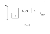
- Figure 2 illustrates the preferred -x/ ⁇ IP/x sequence for use in the methods of the present invention.
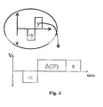
- FIG 3 illustrates schematically how the waveform shown in Figure 2 may be modified to include an additional pair of drive pulses.
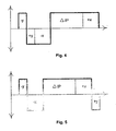
- Figure 4 illustrates one waveform produced by modifying the waveform of Figure 2 in the manner illustrated in Figure 3 .
- Figure 5 illustrates a second waveform produced by modifying the waveform of Figure 2 in the manner illustrated in Figure 3 .
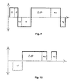
- Figure 6 illustrates schematically how the waveform shown in Figure 5 may be further modified to include an additional pair of drive pulses.
- Figure 7 illustrates one waveform produced by modifying the waveform of Figure 5 in the manner illustrated in Figure 6 .
- Figures 8-10 illustrate three modifications of the waveform shown in Figure 2 to incorporate a period of zero voltage.
- the present invention provides several different improvements in methods for driving electro-optic displays.
- the various different improvements provided by the present invention will normally be described separately, although it will be understood by those skilled in the imaging art that in practice a single display may make use of more than one of these major aspects; for example, a display which uses the limited transitions method of the present invention may also make use of the interrupted scanning method.
- the improvements provided by the present invention can be applied to a wide variety of methods for driving electro-optic displays described in the aforementioned WO 03/044765 and PCT/US2004/10091 , the following description will assume familiarity with the basic driving methods shown in Figures 1-10 of WO 03/044765 and the related description.
- n-PP SS uncompensated n-prepulse slide show
- the black and white flashes which appear on the display during the reset steps of such drive schemes described above are of course visible to the user and may be objectionable to many users.
- the spatial distribution of the two groups is chosen carefully and the pixels are sufficiently small, the user will experience the reset step as an interval of gray on the display (with perhaps some slight flicker), and such a gray interval is typically less objectionable than a series of black and white flashes.
- the pixel in odd-numbered columns may be assigned to one "odd” group and the pixels in the even-numbered columns to the second "even” group.
- the odd pixels could then make use of a drive scheme shown in Figure 9 in which, during the erase step, the pixels are driven to a black state, while the even pixels could make use of a variant of this drive scheme in which, during the erase step, the pixels are driven to a white state.
- Both groups of pixels would then be subjected to an even number of reset pulses during reset step, so that the reset pulses for the two groups are essentially 180° out of phase, and the display appears gray throughout this reset step.
- the odd pixels are driven from black to their final state, while the even pixels are driven from white to their final state.
- the controller In order to ensure that every pixel is reset in the same manner over the long term (and thus that the manner of resetting does not introduce any artifacts on to the display), it is advantageous for the controller to switch the drive schemes between successive images, so that as a series of new images are written to the display, each pixel is written to its final state alternately from black and white states.
- the pixels in odd-numbered rows form the first group and the pixels in even-numbered rows the second group.
- the first group comprises pixels in odd-numbered columns and odd-numbered rows, and even-numbered columns and even-numbered rows
- the second group comprises in odd-numbered columns and even-numbered rows, and even-numbered columns and odd-numbered rows, so that the two groups are disposed in a checkerboard fashion.
- the pixels may be divided into groups which use different reset steps differing in number and frequency of pulses. For example, one group could use a six pulse reset sequence, while the second could use a similar sequence having twelve pulses of twice the frequency.
- the pixels could be divided into four groups, with the first and second groups using the six pulse scheme but 180° out of phase with each other, while the third and fourth groups use the twelve pulse scheme but 180° out of phase with each other.
- a drive scheme which permits any given to assume a non-zero but limited number of successive gray states before touching an optical rail.
- any pixel which has undergone a number of transitions exceeding a predetermined value without touching an extreme optical state, is driven to at least one extreme optical state before driving that pixel to its final optical state.
- a pixel driven to an extreme optical state is driven to the extreme optical state which is closer in gray level to the optical state desired after the transition, assuming of course that this desired optical state is not one of the extreme optical states.
- the maximum number of transitions which a pixel is allowed to undergo without touching an optical rail is set equal to the number of prior optical states taken into account in the transition matrix; such a method requires no extra controller logic or memory.
- Driving methods which limit the maximum number of transitions before touching an optical rail need not significantly increase the time taken for a complete rewriting of the display. For example, consider a four gray level (2 bit) display in which a transition from white to black or vice versa takes 200 msec, so that a general grayscale image flow drive scheme takes this time to completely rewrite the display.
- the only case where a transition needs to be modified in such a display is when a pixel is repeatedly toggled between the two central gray levels. If such a pixel is toggled between the two central gray levels for a number of transitions which exceeds the predetermined number, the limited transitions method of the present invention requires that the next toggling be effected via one optical rail (extreme optical state).
- the transition to the optical rail takes about 70 msec, while the subsequent transition to the gray level takes about 130 msec, so that the total transition time is only about 200 msec.
- the present limited transitions method does not require any increase in transition time as compared with general grayscale image flow.
- Figure 1A shows an even pixel undergoing a transition from black (level 0) to gray level 1. This is achieved with a single white-going pulse (shown of course with a positive gradient in Figure 1A ) designated 1102. Next, the pixel is driven to gray level 3. Since gray level 3 is a dark gray level, according to rule (a) it must be reached by a white-going pulse, and the level 1/level 3 transition can thus be handled by a single white-going pulse 1104, which has an impulse different from that of pulse 1102.
- the pixel is next driven to gray level 4. Since this is a light gray level, by an argument exactly similar to that employed for the level 1/level 3 transition discussed earlier, the level 6/level 4 transition is effected by a single black-going pulse 1110. The next transition is to level 3. Since this is a dark gray level, by an argument exactly similar to that employed for the level 3/level 6 transition discussed earlier, the level 4/level 3 transition is handled by a two-pulse sequence, namely a first black-going pulse 1112, which drives the pixel black (level 0), followed by a second white-going pulse 1114, which drives the pixels from level 0 to the desired level 3.
- the final transition shown in Figure 1A is from level 3 to level 1. Since level 1 is a dark gray level, it must, according to rule (a) be approached by a white-going pulse. Accordingly, applying rules (a) and (c), the level 3/level 1 transition must be handled by a three-pulse sequence comprising a first white-going pulse 1116, which drives the pixel white (level 7), a second black-going pulse 1118, which drives the pixel black (level 0), and a third white-going pulse 1120, which drives the pixel from black to the desired level 1 state.
- Figure 1B shows an odd pixel effecting the same 0-1-3-6-4-3-1 sequence of gray states as the even pixel in Figure 1A . It will be seen, however, that the pulse sequences employed are very different. Rule (b) requires that level 1, a dark gray level, be approached by a black-going pulse. Hence, the 0-1 transition is effected by a first white-going pulse 1122, which drives the pixel white (level 7), followed by a black-going pulse 1124, which drives the pixel from level 7 to the desired level 1.
- the 1-3 transition requires a three-pulse sequence, a first black-going pulse 1126, which drives the pixel black (level 0), a second white-going pulse 1128, which drives the pixel white (level 7), and a third black-going pulse 1130, which drives the pixel from level 7 to the desired level 3.
- level 6 is a light gray level, which according to rule (b) is approached by a white-going pulse
- the level 3/level 6 transition is effected by a two-pulse sequence comprising a black-going pulse 1132, which drives the pixel black (level 0), and a white-going pulse 1134, which drives the pixel to the desired level 6.
- the level 6/level 4 transition is effected by a three-pulse sequence, namely a white-going pulse 1136, which drives the pixel white (level 7), a black-going pulse 1138, which drives the pixel black (level 0) and a white-going pulse 1140, which drives the pixel to the desired level 4.
- the level 4/level transition 3 transition is effected by a two-pulse sequence comprising a white-going pulse 1142, which drives the pixel white (level 7), followed by a black-going pulse 1144, which drives the pixel to the desired level 3.
- the level 3/level 1 transition is effected by a single black-going pulse 1146.
- this drive scheme is a "rail-stabilized gray scale" or “RSGS” drive scheme.
- RSGS rail-stabilized gray scale
- Such a RSGS drive scheme is a special case of a limited transitions drive scheme which ensures that a pixel can only undergo, at most, a number of transitions equal to N/2 (or more accurately (N-1)/2) transitions, where N is the total number of gray levels capable of being displayed, without requiring a transition to take place via an optical rail.
- N is the total number of gray levels capable of being displayed, without requiring a transition to take place via an optical rail.
- Such a drive scheme prevents slight errors in individual transitions (caused, for example, by unavoidable minor fluctuations in voltages applied by drivers) accumulating indefinitely to the point where serious distortion of a gray scale image is apparent to an observer.
- this drive scheme is designed so that even and odd pixels always approach a given intermediate gray level from opposed directions, i.e., the final pulse of the sequence is white-going in one case and black-going in the other. If a substantial area of the display, containing substantially equal numbers of even and odd pixels, is being written to a single gray level, this "opposed directions" feature minimizes flashing of the area.
- a reasonable compromise between energy consumption and the desire to avoid large contiguous areas of pixels of the same group is to have pixels of each group assigned to rectangles, the pixels of which all lie in the same column but extend for several pixels along that column. With such an arrangement, when rewriting areas having the same gray level, discharging and recharging of the column electrodes will only be necessary when shifting from one rectangle to the next.
- the rectangles are 1 x 4 pixels, and are arranged so that rectangles in adjacent columns do not end on the same row, i.e., the rectangles in adjacent columns should have differing "phases".
- the assignment of rectangles in columns to phases may be effected either randomly or in a cyclic manner.
- any areas of the image which are monochrome are simply updated with a single pulse, either black to white or white to black, as part of the overall updating of the display.
- the maximum time taken for rewriting such monochrome areas is only one-half of the maximum time for rewriting areas which require gray to gray transitions, and this feature can be used to advantage for rapid updating of image features such as characters input by a user, drop-down menus etc.
- the controller can check whether an image update requires any gray to gray transitions; if not, the areas of the image which need rewriting can be rewritten using the rapid monochrome update mode.
- a user can have fast updating of input characters, drop-down menus and other user-interaction features of the display seamlessly superimposed upon a slower updating of a general grayscale image.
- a limited transitions drive scheme does not necessarily require the use of counters to measure the number of transitions undergone by each pixel of a display, and does not bar the use of drive schemes (such as the cyclic RSGS drive scheme already described with reference to Figures 1A and 1B ) which require certain transitions to take place via an optical rail even if the predetermined number of transitions has not been reached, provided that the algorithm used to determine the manner of effecting transitions does not permit any pixel to undergo more than the predetermined number of transitions without touching an optical rail.
- the check on the number of transitions undergone by a given pixel without touching an optical rail need not be made at every rewriting of the image on the display, especially in the case of displays (for example in watches) which are updated at frequent intervals.
- the check might be made on only alternate updates, provided that all pixels which either exceeded with predetermined number of transitions or might exceed this number after the next update were driven to optical rails.
- the display controller is a tri-level pulse width modulation (PWM) controller capable of applying -V, 0 or +V to each pixel electrode relative to the common front electrode, which is held at 0.
- PWM pulse width modulation
- the display controller contains two RAM image buffers.
- One buffer (“A") stores the image currently on the display. Normally, the controller is in sleep mode, preserving the data in the RAM and keeping the display drivers inactive. The bistability of the electro-optic medium keeps the same image on the display.
- the controller loads the new image into the second buffer (“B”). Then, for each pixel of the display, the controller looks up (in FLASH memory) a multi-frame drive waveform, based on the desired final state R1 of the pixel (from buffer 'B") and the current, initial state R2 of each pixel (from buffer "A").
- the data in the flash memory file is organized as a three-dimensional array of voltage values, V(R1, R2, frame), where as already indicated R1 and R2 are each integers from 1 to 4 (corresponding to the four available gray levels), and "frame" is the frame number, i.e., the number of the relevant frame within the superframe used for each transition.
- the superframe might be 1 second long, with each frame occupying 20 ms, so that the frame number can range from 1 to 50.
- each of the 800 array entries may have any one of the three possible voltage values, there are a huge number of possible arrays (waveforms), the number being far too large to search exhaustively.
- existing knowledge about the behavior of electro-optic displays, and especially the need for DC balance therein impose additional constraints upon the possible waveforms and enable the search for an optimum or near optimum waveform to be confined within practicable limits.
- the look-up table can store multiple impulses for a given transition, together with a value for the total current provided by each of these impulses, and the controller can maintain, for each pixel, a register arranged to store the algebraic sum of the impulses applied to the pixel since some prior time (for example, since the pixel was last in a black state).
- the controller can examine the register associated with that pixel, determine the current required to DC balance the overall sequence of transitions from the previous black state to the forthcoming black state, and choose that one of the multiple stored impulses for the white/gray to black transition needed which will either accurately reduce the associated register to zero, or at least to as small a remainder as possible (in which case the associated register will retain the value of this remainder and add it to the currents applied during later transitions). It will be apparent that repeated applications of this process can achieve accurate long term DC balancing of each pixel.
- This waveform is clearly DC balanced, but the integral of applied voltage is not zero at every point in time; this integral varies between 0 and ⁇ 4.5 V-sec. However, this waveform DC is balanced in as much as the integral is bounded; the integral never reaches 9 or 18 V-sec, for example.
- impulse has already been defined as meaning the definite integral of voltage with respect to time (in V-sec) applied during a particular interval, usually an addressing pulse or pulse element.
- impulse potential will be used to mean the sum of all impulses applied to the display since an arbitrary starting point (typically the beginning of a series of transitions under consideration. At the starting point, the impulse potential is arbitrarily set to zero, and as impulses are applied the impulse potential rises and falls.
- DC balance is that a waveform is DC balanced if and only if the impulse potential is bounded. Having a bounded impulse potential means that one must be able to say what the impulse potential will be in each of a finite number of possible cases.
- a time-independent controller i. e., a controller in which the impulse of the waveform is influenced only by the initial and final states of the transition under consideration, and not dwell times, temperature, or other factors, such as the R1/R2 controller mentioned above
- the impulse potential can be expressed as a function of a fixed number of prior states, and this provides a working concept of DC balance for controllers for electro-optic displays, i.e., that the impulse potential can be expressed as a function of a finite number of prior and current optical states. Note that the impulse potential of any pixel of the display does not change from the end of one image update to the beginning of another image update, because no voltage is applied during this period.
- the controller applies a fixed impulse (the impulse determined by the data in the flash memory already mentioned), and these fixed impulses can be listed. To list them, it is necessary to enumerate prior state combinations back by at least the number of prior states being used in the controller (i.e. for an R1/R2 controller, the number of prior states used in the enumeration needs to be defined for all combinations of prior states two back).
- each combination of R1 and R2 must leave the electro-optic medium at the same impulse potential, independent of R3.
- the controller has to "know" the impulse potential of the electro-optic medium when it starts the transition being considered, so it can apply the right impulse to produce the proper value of impulse potential following the transition. If the impulse potential in the above example were allowed to vary based on all of R1, R2, and R3, then, in the next transition, there would be no way for the controller to "know” the starting impulse potential, since the R3 information previously used would have been discarded.
- the limited transitions method of the present invention is preferably carried out using an R1/R2 controller (i.e., a controller in which the impulse applied during any transition depends only upon the initial and final gray levels of that transition), and from the foregoing discussion it will be seen that in such a controller the impulse potential must be uniquely defined as a function of R1 only.
- R1/R2 controller i.e., a controller in which the impulse applied during any transition depends only upon the initial and final gray levels of that transition
- This impulse hysteresis produces an inherent "restoring force" tending to bring the electro-optic medium towards middle gray levels, and confounds efforts to drive the medium from state to state with unipolar pulses (as in general gray scale image flow) while still maintaining DC balance.
- the medium rides the three-dimensional R1/R2/impulse hysteresis surface until it reaches an equilibrium. This equilibrium is fixed for each pulse length and is generally in the center of the optical range. For example, it has been found empirically that driving one encapsulated four gray level electro-optic medium from black to dark gray required a 100 ms x -15 V unipolar impulse, but driving it back from dark gray to black required a 300 ms x 15 V unipolar impulse. This waveform was not DC balanced, for obvious reasons.
- a solution to the impulse hysteresis problem is to use a bipolar drive, that is to say to drive the electro-optic medium on a (potentially) non-direct path from one gray level to the next, first applying an impulse to drive the pixel into either optical rail as required to maintain DC balance and then applying a second impulse to reach the desired optical state.
- a bipolar drive that is to say to drive the electro-optic medium on a (potentially) non-direct path from one gray level to the next, first applying an impulse to drive the pixel into either optical rail as required to maintain DC balance and then applying a second impulse to reach the desired optical state.
- the impulse hysteresis phenomenon and the prior state dependence of electro-optic media require that the waveform for each transition vary depending upon the prior state history of the pixel being considered.
- the optimum waveform for each transition may be determined (i.e., the transition table corresponding to the aforementioned data array may be "tuned") by using an initial "guessed" transition matrix to create a waveform, which is used to address the electro-optic medium through a fixed, typically pseudo-random or priorstate-complete series of optical states.
- a program subtracts the actual optical state achieved in each prior state combination from the target gray states for the same combination to compute an error matrix, which is the same dimensions as the transition matrix.
- Each element in the error matrix corresponds to an element in the transition matrix. If an element in the transition matrix is too high, the corresponding element in the error matrix will be pushed higher.
- PID proportional-integral-differential
- control can then be used to drive the error matrix toward zero.
- There are cross-terms (each element in the transition matrix affects more than one element in the error matrix) but these effects are minor and tend to decrease as the magnitudes of the values in the error matrix decrease, as the tuning proceeds through multiple iterations. (Note that sometimes the I or D constants of the PID controller may be set to 0, yielding PI, PD, or P control.)
- TM dimension The correlation between the number of dimensions in the transition matrix ("TM dimension") and the maximum optical error for this waveform was found to be as set out in Table 1 below: Table 1 TM Dimension Maximum Optical Error (L*) 1 10.6 2 3.8 3 2.1 4 1.7
- the data in this table indicate that it is very useful to have more than one dimension in the transition matrix, with a two dimensional matrix being superior to a one dimensional, a three dimensional matrix being superior to a two dimensional, etc.
- the values in the transition matrix could be adjusted as desired, without worrying about DC balance, because the net impulse of the first and third sections of this waveform is always zero.
- the difference in impulse potential between the initial and final state is applied in the middle section of the waveform.
- the transition matrix for this waveform can be tuned with the same PID approach described above.
- the values set for the impulse potentials influence the update speed of the waveform for fixed final gray levels. For example, all the impulse potentials could be set to zero, but this results in a long update time, because the final drive pulse (third section) is always countered by an equally long initial pulse (first section). Thus, the final drive pulse, in this case, cannot be longer than half the total update time.
- By careful selection of impulse potentials it is possible to use a much larger fraction of the total update time for the final pulse; for example, one can achieve final drive pulses occupying more than half, and as much as 80% of the total maximum update time.
- the lengths of the various pulses are selected by computer, using a gradient following optimization method, like PID control, finite difference combination evaluation, etc.
- transitions in electro-optic media are typically temperature sensitive, and it has been found that the uncompensated stability of gray levels versus temperature is increased when all of the transitions to a particular gray level always come from the same optical rail.
- the reason for this is straightforward; as the temperature varies, the switching speed of the electro-optic medium becomes gets faster or slower.
- the dark gray to light gray transition bounces off the black rail, but the white to light gray transition bounces off the white rail. If the switching speed of the medium becomes slower, the light gray state addressed from black will become darker, but the light gray state addressed from black will become lighter.
- This preferred waveform is fully compatible with techniques such as insertion of short pause periods into the waveform to increase impulse resolution, as described below.
- the aforementioned -x/ ⁇ IP/x pulse sequences may be modified to contain additional pulses.
- One such modification allows the inclusion of an additional class of pulses, hereinafter referred to as "y" pulses.
- "y" pulses are characterized by being of the form [+y][-y], where y is an impulse value, and may be either negative or positive (in other words, the form [-y][+y] is equally valid.
- the y pulse is distinct from the previously-described "x" pulses, in that the [-x] and [+x] halves of the "x" pulse pair are disposed before and after the ⁇ IP pulse, whereas the "y” pulses can be disposed at other locations within the pulse sequence.
- a second such modification adds a 0 V "pulse" (i.e., a period when no voltage is applied to the relevant pixel) at an arbitrary point within the pulse sequence to improve the performance of that sequence, by, for example, shifting the gray level resulting from the transition up or down by a small amount, or reducing or changing the impact of prior state information on the final state of the pixel.
- 0 V sections may be inserted either between the different pulse elements, or in the middle of a single pulse element.
- a preferred method for constructing a rail-stabilized waveform, using a transition table as described in the aforementioned WO 03/044765 is as follows:
- Figure 2 shows the basic -x/ ⁇ IP/+x structure of the waveform for one transition, it being assumed for the sake of illustration that the values of both x and ⁇ IP are positive. Unless it is desired to provide a 0 V interval between the ⁇ IP and the +x pulses, it is not necessary to reduce the voltage applied at the junction between these two pulses, so that the ⁇ IP and +x pulses form, in effect, one long positive pulse.
- Figure 3 illustrates symbolically the insertion of a [-y][+y] pair of pulses into the basic -x/ ⁇ IP/+x waveform shown in Figure 2 .
- the -y and +y pulses do not have to be consecutive, but can be inserted at different places into the original waveform. There are two especially advantageous special cases.
- the "-y, +y" pulse pair is placed at the beginning of the -x/ ⁇ IP/+x waveform, before the -x pulse, to produce the waveform shown in Figure 4 .
- the final optical state can be finely tuned by even moderately coarse adjustment of the duration y.
- the value of x can be adjusted for coarse control and the value of y for final control of the final optical state of the electro-optic medium. This is believed to happen because the y pulse augments the -x pulse, thus changing the degree to which the electro-optic medium is pushed into one of its optical rails.
- the degree of pushing into one of the optical rails is known to give fine adjustment of the final optical state after a pulse away from that optical rail (in this case, provided by the x pulse).
- the -y pulse is again placed at the beginning of the -x/ ⁇ IP+x waveform, before the -x pulse, but the +y pulse is placed at the end of the waveform, after the +x pulse.
- the final y pulse provides coarse tuning because the final optical state is very sensitive to the magnitude of y.
- the x pulse provides a finer tuning, since the final optical state typically does not depend as strongly on the magnitude of the drive into the optical rail.
- FIG. 6 illustrates symbolically, in a manner similar to that of Figure 3 , the insertion of a second pair of y-type pulses (denoted “-z", “+z") into the waveform of Figure 5 . It will readily be apparent that since the -z and +z pulses can be introduced at any pulse boundary of the waveform shown in Figure 5 , a large number of different waveforms can result from the introduction of the -z and +z pulses.
- a preferred resulting waveform is shown in Figure 7 ; this type of waveform is useful for fine tuning of the final optical state, for the following reasons.
- the x pulse element is used for fine tuning, and the final optical state can be decreased by increasing x and increased by decreasing x.
- it is undesirable to decrease x beyond a certain point because then the electro-optic medium is not brought sufficiently close to an optical rail, as required for stability of the waveform.
- the +z pulse augments the -x pulse, while the -z pulse maintains the transition at the desired net impulse, thus maintaining an overall DC balanced transition table.
- Any given transition table element may contain zero or more sets of x and/or y pulses.
- the limited transitions method of the present invention may also make use of pause periods between adjacent frames of a transition; such pause periods are discussed in more detail below with reference to the interrupted scanning method of the present invention.
- the pixels are divided into a series of groups (normally a plurality of rows), each of these plurality of groups is selected in succession (i.e., typically the rows of the matrix are scanned) and there is applied to each of the pixels in the selected group either a drive voltage or a non-drive voltage.
- the scanning of all the groups of pixels is completed within a frame period.
- the scanning of the groups of pixels is repeated, and, in a typical electro-optic display, the scanning will be repeated more than once during the group of frames (conveniently referred to as a superframe) required for a complete rewriting of the display.
- a fixed scan rate is used for updating, for example 50 Hz, which allows for 20 msec frames.
- this frame length may provide insufficient resolution for optimal waveform performance.
- frames of length t/2 are desirable, for example 10 msec frames in a normally 20 msec frame length waveform. It is possible to combine frames of differing delay times to generate a pulse resolution of n/2.
- a single frame of length 1.5*t may be inserted at the beginning of the waveform, and a similar frame at the end of the waveform (immediately before the terminating 0 V frame, which should occur at the ordinary frame rate and which is normally used at the end of the waveform to prevent undesirable effects caused by varying residual voltages on pixels).
- the two longer frames can be realized by simply adding a 0.5*t delay time between the scanning of two adjacent frames.
- the waveform would then have the structure:
- the initial and final frames plus their respective delays would amount to 30 msec each.
- the initial and final pulses are allowed to vary by 10 msec in length, by using the following algorithm:
- the initial and final pulses must be start- and end-justified, respectively, for this algorithm to work properly.
- the initial and final pulses may be corresponding parts of a -x/+x pair.
- the effect of the waveform used to effect a transition is modified by the presence of a period of zero voltage (in effect a time delay) during or before any of the pulses in the waveform
- the limited transitions method of the present invention may include periods of zero voltage within or between successive pulses in the waveform, i.e., the waveform may be "non-contiguous" as that term is used above and in the aforementioned PCT/US2004/010091 .
- Figures 8 to 10 illustrate variations of the basic -x/ ⁇ IP/+x waveform of Figure 2 incorporating such zero voltage periods. In the waveform of Figure 8 , a time delay is inserted between the -x pulse and the ⁇ IP pulse.
- a time delay is inserted within the ⁇ IP pulse, or, which amounts to the same thing, the ⁇ IP pulse is split into two separate pulses separated by the time delay.
- the waveform of Figure 10 is similar to that of Figure 9 , except that the time delay is inserted within the +x pulse.
- Time delays can be incorporated into a waveform to achieve optical states not achievable without such delays. Time delays can also be used to fine-tune the final optical state. This fine-tuning ability is important, because in an active matrix drive, the time resolution of each pulse is defined by the scan rate of the display. The time resolution offered by the scan rate can be coarse enough that precise final optical states cannot be achieved without some additional means of fine tuning.
- this invention provides an "interrupted scanning" method for driving an electro-optic display having a plurality of pixels divided into a plurality of groups.
- the method comprises selecting each of the plurality of groups of pixels in succession and applying to each of the pixels in the selected group either a drive voltage or a non-drive voltage, the scanning of all the groups of pixels being completed in a first frame period.
- the scanning of the groups of pixels is repeated during a second frame period (it being understood that any specific pixel may have the drive voltage applied during the first frame period and the non-drive voltage applied during the second frame period, or vice versa ) .
- the scanning of the groups of pixels is interrupted during a pause period between the first and second frame periods, this pause period being not longer than the first or second frame period.
- the first and second frame periods are typically equal in length, and the length of the pause period is typically a sub-multiple (desirably, one half, one fourth etc.) of the length of one of the frame periods.
- the interrupted scanning method may include multiple pause periods between different pairs of adjacent frame periods. Such multiple pause periods are preferably of substantially equal length, and the total length the multiple pause periods is preferably equal to either one complete frame period, or equal to one frame period less one pause period. For example, as discussed in more detail below, one embodiment of the first method might use multiple 20 ms frame periods, and either three or four 5 ms pause periods.
- the groups of pixels will of course typically be the rows of a conventional row/column active matrix pixel array.
- the interrupted scanning method comprises selecting each of the plurality of groups of pixels in succession (i.e., typically, scanning the rows of the matrix) and applying to each of the pixels in the selected group either a drive voltage or a non-drive voltage, the scanning of all the groups of pixels being completed in a first frame period.
- the scanning of the groups of pixels is repeated, and in a typical electro-optic display, the scanning will be repeated more than once during the superframe required for a complete rewriting of the display.
- the scanning of the groups of pixels is interrupted during a pause period between the first and second frame periods, this pause period being not longer than the first or second frame period.
- a drive voltage is only applied to any specific pixel electrode for one line address time during each scan, the drive voltage persists on the pixel electrodes during the time between successive selections of the same line, only slowly decaying, so that the pixel continues to driven during the time when other lines of the matrix are being selected, and the interrupted scanning method relies upon this continued driving of the pixel during its "non-selected" time. Ignoring for the moment the slow decay of the voltage on the pixel electrode during its non-selected time, a pixel which is set to the driving voltage during the frame period immediately preceding the pause period will continue to experience the driving voltage during the pause period, so that for such a pixel the preceding frame period is in effect lengthened by the length of the pause period.
- a pixel which is set to the non-driving (typically zero) voltage during the frame period immediately preceding the pause period will continue to experience the zero voltage during the pause period. It may be desirable to adjust the length of the pause period to allow for the slow decay of the voltage on the pixel electrode in order to ensure that the total impulse delivered to the pixel during the pause period has the desired value.
- a 10 ms pause period may be inserted between two successive 20 ms frames, and this simple modification halves the maximum possible difference between the applied impulse and the impulse ideally needed to complete a given transition, thereby in practice approximately halving the maximum deviation in achieved gray scale level.
- the 10 ms pause period is conveniently inserted after the penultimate frame in each superframe but may be inserted at other points in the superframe if desired.
- the pause periods can of course be of any number and length required to achieve the desired control over the impulse applied.
- the drive scheme could be modified to include three 5 ms pause periods after different 20 ms drive frames, desirably with the addition to the drive scheme of three further 20 ms drive frames not followed by pause periods.
- This modified drive scheme permits one to apply to any given pixel impulses of:
- bistable electro-optic media require application of impulses of both polarities.
- some drive schemes such as slide show drive schemes, before a new image is written to the display, all the pixels of the display are first driven to one extreme optical state, either black or white, and thereafter the pixels are driven to their final gray states by impulses of a single polarity.
- Such drive schemes can be modified in accordance with the interrupted scanning method in the manner already described.
- Other drive schemes require application of impulses of both polarities to drive the pixels to their final gray states.
- the impulses of the two polarities may be applied in separate frames or impulses of the two polarities may be applied in the same frames, for example using a tri-level drive scheme in which the common front electrode is held at a voltage of V/2, while individual pixel electrodes are held at 0, V/2 or V.
- the interrupted scanning method is desirably effected by providing at least two separate pause periods, one following a frame in which impulses of one polarity are applied and the second following a frame in which impulses of the opposed polarity are applied.
- the interrupted scanning method may make use of only a single pause period since, as will be apparent from the foregoing discussion, the effect of including a pause period after a frame is to increase the magnitude of the impulse applied to any pixel to which a driving voltage was applied in the frame, regardless of the polarity of this driving voltage.
- bistable electro-optic media are desirably driven with drive schemes which achieve long term direct current (DC) balance, and such DC balance is conveniently effected using a drive scheme in which a DC balance section, which does not substantially change the gray level of the pixel, is applied before the main drive section, which does change the gray level, the two sections being chosen so that the algebraic sum of the impulses applied is zero or at least very small.
- a DC balance section which does not substantially change the gray level of the pixel
- the main drive section which does change the gray level
- DC balance section it is not necessary that the DC balance section be modified in a manner which is an exact mirror image of the modification of the main drive section, since the DC balance section can have gaps (zero voltage frames) and most electro-optic medium are not harmed by short term DC imbalances.
- DC balance can be achieved by making the first frame of the drive scheme 30 ms in duration. Applying or not applying a driving voltage to a pixel during this frame brings the overall impulse to a multiple of 20 units, so that this impulse can readily be balanced later.
- the first two frames of the drive scheme can similarly be 25 and 30 ms in duration (in either order), again bringing the overall impulse to a multiple of 20 units.
- the interrupted scanning method of the present invention requires a trade-off between increased addressing time caused by the need to include one additional frame in each superframe for each pause period inserted, and the improved control of impulse and hence gray scale produced by the method.
- the interrupted scanning method can provide very substantial improvement in impulse control with only modest increase in addressing time; for example, the drive scheme described above in which a superframe comprising ten 20 ms frames is modified to include three 5 ms pause periods yields a four-fold improvement in impulse accuracy at the cost of less than a 40 per cent increase in addressing time.
- this invention also provides a balanced gray level method for driving an electro-optic display having a plurality of pixels arranged in an array.
- the pixels are driven with a pulse width modulated waveform capable of applying a plurality of differing impulses.
- Drive circuitry stores data indicating whether application of a given impulse will produce a gray level higher or lower than a desired gray level.
- the impulses applied to the two pixels are adjusted to that one pixel is below the desired gray level, while the other pixel is above the desired gray level.
- the pixels are divided into two groups, hereinafter designated “even” and “odd”.
- the two groups of pixels may be arranged in a checkerboard pattern (so that the pixels in each row and column alternate between the two groups) or in other arrangements as described in the aforementioned WO 03/044765 , provided that each pixel has at least one neighbor of the opposite group, and different drive schemes are used for the two groups. If the stored data indicates that one of the available impulses will produce substantially the desired gray level transition, this impulse is applied for that transition for both the even and odd pixels.
- the stored data indicates that the impulse required for a particular gray level transition is substantially half-way between two of the available impulses, one of these impulses is used for the transition in even pixels and the other of these impulses is used for the transition in odd pixels.
- two adjacent pixels are intended to be in the same gray state (the condition where precise control of gray scale is of maximum importance) one of these pixels will have a gray level slightly above the desired level, while the other will have a gray level slightly below the desired level. Ocular and optical averaging will result in an average of the two gray levels being seen, thus producing an apparent gray level closer to the desired level than can be achieved with the available impulses.
- this balanced gray level method uses small-signal spatial dithering (applied to correct errors in applied impulse) superimposed on large signal true gray scale to increase by a factor of two the available impulse levels. Since each pixel is still at approximately the correct gray scale level, the effective resolution of the display is not compromised.
- the pixels of the display are already divided into two groups and different drive schemes are applied to the two groups, so that the magnitude of the impulses needed to achieve the desired gray level will be different of the two groups.
- Such "two group” drive schemes can be modified in accordance with the balanced gray level method but the detailed implementation of the method differs somewhat from the simple case discussed above. Instead of simply comparing the available impulses with that required for the desired transition, one calculates the errors in gray scale for the two groups separately, takes the arithmetic average of the errors, and determines whether this arithmetic average would be reduced by shifting one of the groups to a different available impulse. Note that in this case, the reduction in arithmetic average may differ depending upon which group is shifted to a different impulse, and obviously whichever shift produces the smaller average should be effected.
- this method can be thought of as small-signal spatial dithering implemented on top of large signal intrinsic gray scale, with the small signal dithering used to correct for errors in impulse due to the limitation of the pulse width modulation drive scheme used. Because each pixel is still approximately at the correct gray level in this scheme, and the corrections are only to correct for impulse rounding errors, effective display resolution is not compromised. To put it another way, this method implements small signal spatial dithering on top of large signal true gray scale.
- the various methods of the present invention may make use of various additional variations and techniques described in the aforementioned applications, especially the aforementioned WO 03/044765 and PCT/US2004/010091 . It will be appreciated that in the overall waveform used to drive an electro-optic display, in at least some cases certain transitions may be effected in accordance with the various methods of the present invention, while other transitions may not make use of the methods of the present invention but may make use of other types of transitions described below. For example, the various methods of the present invention may make use of any one or more of:
Landscapes
- Engineering & Computer Science (AREA)
- Physics & Mathematics (AREA)
- Computer Hardware Design (AREA)
- General Physics & Mathematics (AREA)
- Theoretical Computer Science (AREA)
- Control Of Indicators Other Than Cathode Ray Tubes (AREA)
- Electrochromic Elements, Electrophoresis, Or Variable Reflection Or Absorption Elements (AREA)
- Liquid Crystal Display Device Control (AREA)
Abstract
Description
- This invention relates to methods for driving electro-optic displays. The methods of the present invention are especially, though not exclusively, intended for use in driving bistable electrophoretic displays.
- This application is closely related to International Applications
PCT/US02/37241 (Publication No.WO 03/044765 PCT/US2004/10091 , and the following description will assume that the reader is familiar with the contents of these documents. - The term "electro-optic" as applied to a material or a display, is used herein in its conventional meaning in the imaging art to refer to a material having first and second display states differing in at least one optical property, the material being changed from its first to its second display state by application of an electric field to the material. Although the optical property is typically color perceptible to the human eye, it may be another optical property, such as optical transmission, reflectance, luminescence or, in the case of displays intended for machine reading, pseudo-color in the sense of a change in reflectance of electromagnetic wavelengths outside the visible range.
- The term "gray state" is used herein in its conventional meaning in the imaging art to refer to a state intermediate two extreme optical states of a pixel, and does not necessarily imply a black-white transition between these two extreme states. For example, several of the patents and published applications referred to below describe electrophoretic displays in which the extreme states are white and deep blue, so that an intermediate "gray state" would actually be pale blue. Indeed, as already mentioned the transition between the two extreme states may not be a color change at all.
- The terms "bistable" and "bistability" are used herein in their conventional meaning in the imaging art to refer to displays comprising display elements having first and second display states differing in at least one optical property, and such that after any given element has been driven, by means of an addressing pulse of finite duration, to assume either its first or second display state, after the addressing pulse has terminated, that state will persist for at least several times, for example at least four times, the minimum duration of the addressing pulse required to change the state of the display element. It is shown in International Application
WO 02/079869 - The term "impulse" is used herein in its conventional meaning in the imaging art of the integral of voltage with respect to time. However, some bistable electro-optic media act as charge transducers, and with such media an alternative definition of impulse, namely the integral of current over time (which is equal to the total charge applied) may be used. The appropriate definition of impulse should be used, depending on whether the medium acts as a voltage-time impulse transducer or a charge impulse transducer.
- As described in the aforementioned
WO 03/044765 PCT/US2004/10091 , several types of electro-optic displays are known, for example the rotating bichromal member type as described, for example, inU.S. Patents Nos. 5,808,783 ;5,777,782 ;5,760,761 ;6,054,071 6,055,091 ;6,097,531 ;6,128,124 ;6,137,467 ; and6,147,791 and the electrochromic type; see, for example O'Regan, B., et al., Nature 1991, 353, 737; and Wood, D., Information Display, 18(3), 24 (March 2002). See also Bach, U., et al., Adv. Mater., 2002, 14(11), 845. Nanochromic films of this type are also described, for example, inU.S. Patent No. 6,301,038 , International Application Publication No.WO 01/27690 U.S. Patent Application 2003/0214695 . - Another type of electro-optic display, which has been the subject of intense research and development for a number of years, is the particle-based electrophoretic display. Numerous patents and applications assigned to or in the names of the Massachusetts Institute of Technology (MIT) and E Ink Corporation describe such displays; see for example,
U.S. Patents Nos. 5,930,026 ;5,961,804 ;6,017,584 ;6,067,185 ;6,118,426 ;6,120,588 ;6,120,839 ;6,124,851 ;6,130,773 ;6,130,774 ;6,172,798 ;6,177,921 ;6,232,950 ;6,249,721 ;6,252,564 ;6,262,706 ;6,262,833 ;6,300,932 ;6,312,304 ;6,312,971 ;6,323,989 ;6,327,072 ;6,376,828 ;6,377,387 ;6,392,785 ;6,392,786 ;6,413,790 ;6,422,687 ;6,445,374 ;6,445,489 ;6,459,418 ;6,473,072 ;6,480,182 ;6,498,114 ;6,504,524 ;6,506,438 ;6,512,354 ;6,515,649 ;6,518,949 ;6,521,489 ;6,531,997 ;6,535,197 ;6,538,801 ;6,545,291 ;6,580,545 ;6,639,578 ;6,652,075 ;6,657,772 ;6,664,944 ;6,680,725 ;6,683,333 ;6,704,133 ;6,710,540 ;6,721,083 ;6,724,519 ; and6,727,881 ; andU.S. Patent Applications Publication Nos. 2002/0019081 ;2002/0021270 ;2002/0053900 ;2002/0060321 ;2002/0063661 ;2002/0063677 ;2002/0090980 ;2002/0106847 ;2002/0113770 ;2002/0130832 ;2002/0131147 ;2002/0145792 ;2002/0171910 ;2002/0180687 ;2002/0180688 ;2002/0185378 ;2003/0011560 ;2003/0011868 ;2003/0020844 ;2003/0025855 ;2003/0034949 ;2003/0038755 ;2003/0053189 ;2003/0102858 ;2003/0132908 ;2003/0137521 ;2003/0137717 ;2003/0151702 ;2003/0189749 ;2003/0214695 ;2003/0214697 ;2003/0222315 ;2004/0008398 ;2004/0012839 ;2004/0014265 ;2004/0027327 ;2004/0075634 ; and2004/0094422 ; and International Applications Publication Nos.WO 99/67678 WO 00/05704 WO 00/38000 WO 00/38001 WO00/36560 WO 00/67110 WO 00/67327 WO 01/07961 WO 01/08241 WO 03/092077 WO 03/107315 WO 2004/017035 ; andWO 2004/023202 . - Many of the aforementioned patents and applications recognize that the walls surrounding the discrete microcapsules in an encapsulated electrophoretic medium could be replaced by a continuous phase, thus producing a so-called "polymer-dispersed electrophoretic display" in which the electrophoretic medium comprises a plurality of discrete droplets of an electrophoretic fluid and a continuous phase of a polymeric material, and that the discrete droplets of electrophoretic fluid within such a polymer-dispersed electrophoretic display may be regarded as capsules or microcapsules even though no discrete capsule membrane is associated with each individual droplet; see for example, the aforementioned 2002/0131147. Accordingly, for purposes of the present application, such polymer-dispersed electrophoretic media are regarded as sub-species of encapsulated electrophoretic media.
- A related type of electrophoretic display is a so-called "microcell electrophoretic display". In a microcell electrophoretic display, the charged particles and the suspending fluid are not encapsulated within capsules but instead are retained within a plurality of cavities formed within a carrier medium, typically a polymeric film. See, for example, International Application Publication No.
WO 02/01281 U.S. Patent Application Publication No. 2002/0075556 , both assigned to Sipix Imaging, Inc. - Although electrophoretic media are often opaque (since, for example, in many electrophoretic media, the particles substantially block transmission of visible light through the display) and operate in a reflective mode, many electrophoretic displays can be made to operate in a so-called "shutter mode" in which one display state is substantially opaque and one is light-transmissive. See, for example, the aforementioned
U.S. Patents Nos. 6,130,774 and6,172,798 , andU.S. Patents Nos. 5,872,552 ;6,144,361 ;6,271,823 ;6,225,971 ; and6,184,856 . Dielectrophoretic displays, which are similar to electrophoretic displays but rely upon variations in electric field strength, can operate in a similar mode; seeU.S. Patent No. 4,418,346 . Other types of electro-optic displays may also be capable of operating in shutter mode. - The bistable or multi-stable behavior of particle-based electrophoretic displays, and other electro-optic displays displaying similar behavior (such displays may hereinafter for convenience be referred to as "impulse driven displays"), is in marked contrast to that of conventional liquid crystal ("LC") displays. Twisted nematic liquid crystals act are not bi- or multi-stable but act as voltage transducers, so that applying a given electric field to a pixel of such a display produces a specific gray level at the pixel, regardless of the gray level previously present at the pixel. Furthermore, LC displays are only driven in one direction (from non-transmissive or "dark" to transmissive or "light"), the reverse transition from a lighter state to a darker one being effected by reducing or eliminating the electric field. Finally, the gray level of a pixel of an LC display is not sensitive to the polarity of the electric field, only to its magnitude, and indeed for technical reasons commercial LC displays usually reverse the polarity of the driving field at frequent intervals. In contrast, bistable electro-optic displays act, to a first approximation, as impulse transducers, so that the final state of a pixel depends not only upon the electric field applied and the time for which this field is applied, but also upon the state of the pixel prior to the application of the electric field.
- It might at first appear that the ideal method for addressing such an impulse-driven electro-optic display would be so-called "general grayscale image flow" in which a controller arranges each writing of an image so that each pixel transitions directly from its initial gray level to its final gray level. However, inevitably there is some error in writing images on an impulse-driven display. Some such errors encountered in practice include:
- (a) Prior State Dependence; With at least some electro-optic media, the impulse required to switch a pixel to a new optical state depends not only on the current and desired optical state, but also on the previous optical states of the pixel.
- (b) Dwell Time Dependence; With at least some electro-optic media, the impulse required to switch a pixel to a new optical state depends on the time that the pixel has spent in its various optical states. The precise nature of this dependence is not well understood, but in general, more impulse is required that longer the pixel has been in its current optical state.
- (c) Temperature Dependence; The impulse required to switch a pixel to a new optical state depends heavily on temperature.
- (d) Humidity Dependence; The impulse required to switch a pixel to a new optical state depends, with at least some types of electro-optic media, on the ambient humidity.
- (e) Mechanical Uniformity; The impulse required to switch a pixel to a new optical state may be affected by mechanical variations in the display, for example variations in the thickness of an electro-optic medium or an associated lamination adhesive. Other types of mechanical non-uniformity may arise from inevitable variations between different manufacturing batches of medium, manufacturing tolerances and materials variations.
- (f) Voltage Errors; The actual impulse applied to a pixel will inevitably differ slightly from that theoretically applied because of unavoidable slight errors in the voltages delivered by drivers.
- As described in the aforementioned
WO 03/044765 PCT/US2004/10091 , general grayscale image flow suffers from an "accumulation of errors" phenomenon which may produce deviations in gray levels apparent to the average observer on certain types of images. This accumulation of errors phenomenon applies to errors of all the types listed above. As described in the aforementioned2003/0137521 - Almost all electro-optic medium have a built-in resetting (error limiting) mechanism, namely their extreme (typically black and white) optical states, which function as "optical rails". After a specific impulse has been applied to a pixel of an electro-optic display, that pixel cannot get any whiter (or blacker). For example, in an encapsulated electrophoretic display, after a specific impulse has been applied, all the electrophoretic particles are forced against one another or against the capsule wall, and cannot move further, thus producing a limiting optical state or optical rail. Because there is a distribution of electrophoretic particle sizes and charges in such a medium, some particles hit the rails before others, creating a "soft rails" phenomenon, whereby the impulse precision required is reduced when the final optical state of a transition approaches the extreme black and white states, whereas the optical precision required increases dramatically in transitions ending near the middle of the optical range of the pixel.
- Various types of drive schemes for electro-optic displays are known which take advantage of optical rails. For example,
Figures 9 and10 of the aforementionedWO 03/044765 U.S. Patent No. 6,531,997 ) that a similar drive scheme be employed in which only the pixels, whose optical states need to be changed in the new image, be driven to the optical rails. However, this type of "limited slide show" drive scheme is, if anything, even more distracting to the viewer, since the solid flashing of a normal slide show drive scheme is replaced by image dependent flashing, in which features of the old image and the new image flash in reverse color on the screen before the new image is written. - Obviously, a pure general grayscale image flow drive scheme cannot rely upon using the optical rails to prevent errors in gray levels since in such a drive scheme any given pixel can undergo an infinitely large number of changes in gray level without ever touching either optical rail.
- In one aspect, this invention seeks to provide methods for achieving control of gray levels in electro-optic displays which achieve stability of gray levels similar to those achieved by slide show drive schemes but which do not suffer from the distracting flashing of slide show drive schemes. Preferred methods of the present invention can give the viewer a visual experience similar to that provided by a pure general grayscale image flow drive scheme.
- In another aspect, this invention seeks to provide methods for achieving fine control of gray levels in displays driven by pulse width modulation.
- When driving an active matrix display having a bistable electro-optic medium to write gray scale images thereon, it is desirable to be able to apply a precise amount of impulse to each pixel, so as to achieve accurate control of the gray scale displayed. The driving method used may rely modulation of the voltage applied to each pixel and/or modulation of the "width" (duration) for which the voltage is applied. Since voltage modulated drivers and their associated power supplies are relatively costly, pulse width modulation is commercially attractive. However, during the scanning of an active matrix display using such pulse width modulation, conventional driver circuitry only allows one to apply a single voltage to any given pixel during any one scan of the matrix. Consequently, pulse width modulation driving of active matrix displays is effected by scanning the matrix multiple times, with the drive voltage being applied during none, some or all of the scans, depending upon the change desired in the gray level of the specific pixel. Each scan may be regarded as a frame of the drive waveform, with the complete addressing pulse being a superframe formed by a plurality of successive frames. It should be noted that, although the drive voltage is only applied to any specific pixel electrode for one line address time during each scan, the drive voltage persists on the pixel electrodes during the time between successive selections of the same line, only slowly decaying, so that the pixel is driven between successive selections of the same line.
- As already mentioned, each row of the matrix needs to be individually selected during each frame so that for high resolution displays (for example, 800 x 600 pixel displays) in practice the frame rate cannot exceed about 50 to 100 Hz; thus each frame typically lasts 10 to 20 ms. Frames of this length lead to difficulties in fine control of gray scale with many fast switching electro-optic medium. For example, some encapsulated electrophoretic media substantially complete a switch between their extreme optical states (a transition of about 30 L* units) within about 100 ms, and with such a medium a 20 ms frame corresponds to a gray scale shift of about 6 L* units. Such a shift is too large for accurate control of gray scale; the human eye is sensitive to differences in gray levels of about 1 L* unit, and controlling the impulse only in graduations equivalent to about 6 L* units is likely to give rise to visible artifacts, such as "ghosting" due to prior state dependence of the electro-optic medium. More specifically, ghosting may be experienced because, as discussed in some of the aforementioned patents and applications, the variation of gray level with applied impulse is not linear, and the total impulse needed for any specific change in gray level may vary with the time at which the impulse is applied and the intervening gray levels. For example, in a simple 4 gray level (2 bit) display having gray levels 0 (black), 1 (dark gray), 2 (light gray) and 3 (white), driven by a simple pulse width modulation drive scheme, these non-linearities may result in the actual gray level achieved after a notional 0-2 transition being different from the gray level achieved after a notional 1-2 transition, with the production of highly undesirable visual artifacts. This invention provides methods for achieving fine control of gray levels in displays driven by pulse width modulation, thus avoiding the aforementioned problems.
- Accordingly, in one aspect, this invention provides a method for driving an electro-optic display having at least one pixel capable of achieving any one of at least four different gray levels including two extreme optical states. The method comprises:
- displaying a first image on the display; and
- rewriting the display to display a second image thereon,
- wherein, during the rewriting of the display any pixel which has undergone a number of transitions exceeding a predetermined value, the predetermined value being at least one, without touching an extreme optical state, is driven to at least one extreme optical state before driving that pixel to its final optical state in the second image.
- This method may hereinafter for convenience be referred to as the "limited transitions method" of the present invention.
- In one form of this limited transitions method, the rewriting of the display is effected such that, once a pixel has been driven from one extreme optical state towards the opposed extreme optical state by a pulse of one polarity, the pixel does not receive a pulse of the opposed polarity until it has reached the opposed extreme optical state.
- Also, in the limited transitions methods, the predetermined value (predetermined number of transitions) is not greater than N/2, where N is the total number of gray levels capable of being displayed by a pixel. The limited transitions method may be effected using a tri-level driver, i.e., the rewriting of the display may be effected by applying to the or each pixel any one or more of voltages -V, 0 and . +V. The limited transitions method may also be DC-balanced, i.e., the rewriting of the display may be effected such that, for any series of transitions undergone by a pixel, the integral of the applied voltage with time is bounded.
- In the limited transitions method of the present invention, the rewriting of the display may be effected such that the impulse applied to a pixel during a transition depends only upon the initial and final gray levels of that transition. Alternatively, the method may be adapted to take account of other states of the display, as described in more detail below. In one preferred form of the limited transitions method, for at least one transition undergone by the at least one pixel from a gray level R2 to a gray level R1, there is applied to the pixel a sequence of impulses of the form:
- -TM(R1,R2) IP(R1)-IP(R2) TM(R1,R2)
where "IP(Rx)" represents the relevant value from an impulse potential matrix having one value for each gray level, and TM(R1,R2) represents the relevant value from a transition matrix having one value for each R1/R2 combination. (For convenience, impulse sequences of this type may hereinafter be abbreviated as "-x/ΔIP/x" sequences.) Such -x/ΔIP/x sequences may be used for all transitions in which the initial and final gray levels are different. Also, in such -x/ΔIP/x sequences, the final "x" section may occupy more than one half of the maximum update time. The TM(R1,R2) or x values may be chosen such that the sign of each value is dependent only upon R1; in particular, these values may be chosen to be positive for one or more light gray levels and negative for one or more dark gray levels so that gray levels other than the two extreme optical states are approached from the direction of the nearer extreme optical state. - The aforementioned -x/ΔIP/x sequences may contain additional pulses. In particular, such sequences may comprise an additional pair of pulses of the form [+y][-y], where y is an impulse value, which may be either negative or positive, the [+y] and [-y] pulses being inserted into the -x/ΔIP/x sequence. The sequence may further comprise a second additional pair of pulses of the form [+z][-z], where z is an impulse value different from y and may be either negative or positive, the [+z] and [-z] pulses being inserted into the -x/ΔIP/x sequence. The -x/ΔIP/x sequences may further comprise a period when no voltage is applied to the pixel. This "no voltage" period may occur between two elements of the -x/ΔIP/x sequence, or within a single element thereof. The -x/ΔIP/x sequences may include two or more "no voltage" periods.
- When using the aforementioned -x/ΔIP/x sequences, the display may comprise a plurality of pixels divided into a plurality of groups, and the transition may be effected by (a) selecting each of the plurality of groups of pixels in succession and applying to each of the pixels in the selected group either a drive voltage or a non-drive voltage, the scanning of all the groups of pixels being completed in a first frame period; (b) repeating the scanning of the groups of pixels during a second frame period; and (c) interrupting the scanning of the groups of pixels during a pause period between the first and second frame periods, this pause period being not longer than the first or second frame period.
- In the limited transitions method, the rewriting of the display may be effected such that a transition to a given gray level is always effected by a final pulse of the same polarity. In particular, gray levels other than the two extreme optical states may be approached from the direction of the nearer extreme optical state.
- This invention also provides a method for driving an electro-optic display having a plurality of pixels divided into a plurality of groups. This method comprises:
- (a) selecting each of the plurality of groups of pixels in succession and applying to each of the pixels in the selected group either a drive voltage or a non-drive voltage, the scanning of all the groups of pixels being completed in a first frame period;
- (b) repeating the scanning of the groups of pixels during a second frame period; and
- (c) interrupting the scanning of the groups of pixels during a pause period between the first and second frame periods, this pause period being not longer than the first or second frame period.
- This method may hereinafter for convenience be referred to as the "interrupted scanning" method of the present invention.
- In such an interrupted scanning method, typically the first and second frame periods are equal in length. The length of the pause period may be a sub-multiple of the length of one of the first and second frame periods. The interrupted scanning method may include multiple pause periods; thus the method may comprise scanning the groups of pixels during at least first, second and third frame periods, and interrupting the scanning of the groups of pixels during at least first and second pause periods between successive frame periods. The first, second and third frame periods may be substantially equal in length, and the total length of the pause periods be equal to one frame period or one frame period minus one pause period. Typically, in the interrupted scanning method, the pixels are arranged in a matrix having a plurality of rows and a plurality of columns with each pixel defined by the intersection of a given row and a given column, and each group of pixels comprises one row or one column of the matrix. The interrupted scanning method is preferably DC balanced, i.e., the scanning of the display is preferably effected such that, for any series of transitions undergone by a pixel, the integral of the applied voltage with time is bounded.
- In another aspect, this invention provides a method for driving an electro-optic display having a plurality of pixels, the pixels being driven with a pulse width modulated waveform capable of applying a plurality of differing impulses to each pixel. This method comprises:
- (a) storing data indicating whether application of a given impulse to a pixel will produce a gray level higher or lower than a desired gray level;
- (b) detecting when two adjacent pixels are both required to be in the same gray level; and
- (c) adjusting the impulses applied to the two pixels so that one pixel is below the desired gray level, while the other pixel is above the desired gray level.
- This method may hereinafter for convenience be referred to as the "balanced gray level" method of the present invention.
- In this method, the pixels may be divided into two groups such that each pixel has at least one neighbor of the opposite group, and different drive schemes be used for the two groups.
- Each the methods of the present invention as described above may be carried out with any of the aforementioned types of electro-optic media. Thus, the methods of the present invention may be used with electro-optic displays comprising an electrochromic or rotating bichromal member electro-optic medium, an encapsulated electrophoretic medium, or a microcell electrophoretic medium. Other types of electro-optic media may also be employed.
-
Figures 1A and 1B illustrate two parts of a limited transitions drive scheme of the present invention. -
Figure 2 illustrates the preferred -x/ΔIP/x sequence for use in the methods of the present invention. -
Figure 3 illustrates schematically how the waveform shown inFigure 2 may be modified to include an additional pair of drive pulses. -
Figure 4 illustrates one waveform produced by modifying the waveform ofFigure 2 in the manner illustrated inFigure 3 . -
Figure 5 illustrates a second waveform produced by modifying the waveform ofFigure 2 in the manner illustrated inFigure 3 . -
Figure 6 illustrates schematically how the waveform shown inFigure 5 may be further modified to include an additional pair of drive pulses. -
Figure 7 illustrates one waveform produced by modifying the waveform ofFigure 5 in the manner illustrated inFigure 6 . -
Figures 8-10 illustrate three modifications of the waveform shown inFigure 2 to incorporate a period of zero voltage. - From the foregoing, it will be apparent that the present invention provides several different improvements in methods for driving electro-optic displays. In the description below, the various different improvements provided by the present invention will normally be described separately, although it will be understood by those skilled in the imaging art that in practice a single display may make use of more than one of these major aspects; for example, a display which uses the limited transitions method of the present invention may also make use of the interrupted scanning method. Furthermore, since the improvements provided by the present invention can be applied to a wide variety of methods for driving electro-optic displays described in the aforementioned
WO 03/044765 PCT/US2004/10091 , the following description will assume familiarity with the basic driving methods shown inFigures 1-10 ofWO 03/044765 Figures 9 and10 of this application describe so-called uncompensated n-prepulse slide show (n-PP SS) waveforms having three basic sections. First, the pixels are erased to a uniform optical state, typically either white or black. Next, the pixels are driven back and forth between two optical states, again typically white and black. Finally, the pixel is addressed to a new optical state, which may be one of several gray states. The final (or writing) pulse is referred to as the addressing pulse, and the other pulses (the first (or erasing) pulse and the intervening (or blanking) pulses) are collectively referred to as prepulses - One major shortcoming of this type of waveform is that it has large-amplitude optical flashes between images. This can be improved by shifting the update sequence by one superframe time for half of the pixels, and interleaving the pixels at high resolution, as discussed in
WO 03/044765 Figures 9 and10 thereof. Possible patterns include every other row, every other column, or a checkerboard pattern. Note, this does not mean using the opposite polarity, i.e. "from black" versus "from white", since this would result in non-matching gray scales on neighboring pixels. Instead, this can be accomplished by delaying the start of the update by one "superframe" (a grouping of frames equivalent to the maximum length of a black-white update) for half of the pixels (i.e. the first set of pixels completes the erase pulse, then the second set of pixels begin the erase pulse as the first set of pixels begin the first blanking pulse). This will require the addition of one superframe for the total update time, to allow for this synchronization. - To avoid the aforementioned flashing problems of the drive schemes shown in
Figures 9 and10 ofWO 03/044765 WO 03/044765 - The black and white flashes which appear on the display during the reset steps of such drive schemes described above are of course visible to the user and may be objectionable to many users. To lessen the visual effect of such reset steps, it is convenient to divide the pixels of the display into two (or more) groups and to apply different types of reset pulses to the different groups. More specifically, if it necessary to use reset pulses which drive any given pixel alternately black and white, it is convenient to divide the pixels into at least two groups and to arrange the drive scheme so that one group of pixels are driven white at the same time that another group are driven black. Provided the spatial distribution of the two groups is chosen carefully and the pixels are sufficiently small, the user will experience the reset step as an interval of gray on the display (with perhaps some slight flicker), and such a gray interval is typically less objectionable than a series of black and white flashes.
- For example, in one form of such a "two group reset" step, the pixel in odd-numbered columns may be assigned to one "odd" group and the pixels in the even-numbered columns to the second "even" group. The odd pixels could then make use of a drive scheme shown in
Figure 9 in which, during the erase step, the pixels are driven to a black state, while the even pixels could make use of a variant of this drive scheme in which, during the erase step, the pixels are driven to a white state. Both groups of pixels would then be subjected to an even number of reset pulses during reset step, so that the reset pulses for the two groups are essentially 180° out of phase, and the display appears gray throughout this reset step. Finally, during the writing of the second image at step, the odd pixels are driven from black to their final state, while the even pixels are driven from white to their final state. In order to ensure that every pixel is reset in the same manner over the long term (and thus that the manner of resetting does not introduce any artifacts on to the display), it is advantageous for the controller to switch the drive schemes between successive images, so that as a series of new images are written to the display, each pixel is written to its final state alternately from black and white states. - Obviously, a similar scheme can be used in which the pixels in odd-numbered rows form the first group and the pixels in even-numbered rows the second group. In a further similar drive scheme, the first group comprises pixels in odd-numbered columns and odd-numbered rows, and even-numbered columns and even-numbered rows, while the second group comprises in odd-numbered columns and even-numbered rows, and even-numbered columns and odd-numbered rows, so that the two groups are disposed in a checkerboard fashion.
- Instead of or in addition to dividing the pixels into two groups and arranging for the reset pulses in one group to be 180° out of phase with those of the other group, the pixels may be divided into groups which use different reset steps differing in number and frequency of pulses. For example, one group could use a six pulse reset sequence, while the second could use a similar sequence having twelve pulses of twice the frequency. In a more elaborate scheme, the pixels could be divided into four groups, with the first and second groups using the six pulse scheme but 180° out of phase with each other, while the third and fourth groups use the twelve pulse scheme but 180° out of phase with each other.
- In accordance with the limited transitions method of the present invention, further reductions in flashing problems may be effected by using a drive scheme which permits any given to assume a non-zero but limited number of successive gray states before touching an optical rail. In such a drive scheme, when the display is rewritten to display a new image thereon, any pixel, which has undergone a number of transitions exceeding a predetermined value without touching an extreme optical state, is driven to at least one extreme optical state before driving that pixel to its final optical state. In a preferred form of such a drive scheme, a pixel driven to an extreme optical state is driven to the extreme optical state which is closer in gray level to the optical state desired after the transition, assuming of course that this desired optical state is not one of the extreme optical states. Also, in a preferred form of such a drive scheme using a look-up table as previously described, the maximum number of transitions which a pixel is allowed to undergo without touching an optical rail (extreme optical state) is set equal to the number of prior optical states taken into account in the transition matrix; such a method requires no extra controller logic or memory.
- Driving methods which limit the maximum number of transitions before touching an optical rail need not significantly increase the time taken for a complete rewriting of the display. For example, consider a four gray level (2 bit) display in which a transition from white to black or vice versa takes 200 msec, so that a general grayscale image flow drive scheme takes this time to completely rewrite the display. The only case where a transition needs to be modified in such a display is when a pixel is repeatedly toggled between the two central gray levels. If such a pixel is toggled between the two central gray levels for a number of transitions which exceeds the predetermined number, the limited transitions method of the present invention requires that the next toggling be effected via one optical rail (extreme optical state). It has been found that in such a case the transition to the optical rail takes about 70 msec, while the subsequent transition to the gray level takes about 130 msec, so that the total transition time is only about 200 msec. Thus, the present limited transitions method does not require any increase in transition time as compared with general grayscale image flow.
- A limited transitions drive method which reduces the objectionable effects of reset steps will now be described with reference to
Figures 1A and 1B . In this scheme, the pixels are again divided into two groups, with the first (even) group following the drive scheme shown inFigure 1A and the second (odd) group following the drive scheme shown inFigure 1B . Also in this scheme, all the gray levels intermediate black and white are divided into a first group of contiguous dark gray levels adjacent the black level, and a second group of contiguous light gray levels adjacent the white level, this division being the same for both groups of pixels. Desirably but not essentially, there are the same number of gray levels in these two groups; if there are an odd number of gray levels, the central level may be arbitrarily assigned to either group. For ease of illustration,Figures 1A and 1B show this drive scheme applied to an eight-level gray scale display, the levels being designated 0 (black) to 7 (white);gray levels gray levels - In the drive scheme of
Figures 1A and 1B , gray to gray transitions are handled according to the following rules: - (a) in the first, even group of pixels, in a transition to a dark gray level, the last pulse applied is always a white-going pulse (i.e., a pulse having a polarity which tends to drive the pixel from its black state to its white state), whereas in a transition to a light gray level, the last pulse applied is always a black-going pulse;
- (b) in the second, odd group of pixels, in a transition to a dark gray level, the last pulse applied is always a black-going pulse, whereas in a transition to a light gray level, the last pulse applied is always a white-going pulse;
- (c) in all cases, a black-going pulse may only succeed a white-going pulse after a white state has been attained, and a white-going pulse may only succeed a black-going pulse after a black state has been attained; and
- (d) even pixels may not be driven from a dark gray level to black by a single black-going pulse nor odd pixels from a light gray level to white using a single white-going pulse.
- The application of these rules allows each gray to gray transition to be effected using a maximum of three successive pulses. For example,
Figure 1A shows an even pixel undergoing a transition from black (level 0) togray level 1. This is achieved with a single white-going pulse (shown of course with a positive gradient inFigure 1A ) designated 1102. Next, the pixel is driven togray level 3. Sincegray level 3 is a dark gray level, according to rule (a) it must be reached by a white-going pulse, and thelevel 1/level 3 transition can thus be handled by a single white-goingpulse 1104, which has an impulse different from that ofpulse 1102. - The pixel is now driven to
gray level 6. Since this is a light gray level, it must, by rule (a) be reached by a black-going pulse. Accordingly, application of rules (a) and (c) requires that thislevel 3/level 6 transition be effected by a two-pulse sequence, namely a first white-goingpulse 1106, which drives the pixel white (level 7), followed by a second black-goingpulse 1108, which drives the pixel fromlevel 7 to the desiredlevel 6. - The pixel is next driven to
gray level 4. Since this is a light gray level, by an argument exactly similar to that employed for thelevel 1/level 3 transition discussed earlier, thelevel 6/level 4 transition is effected by a single black-goingpulse 1110. The next transition is tolevel 3. Since this is a dark gray level, by an argument exactly similar to that employed for thelevel 3/level 6 transition discussed earlier, thelevel 4/level 3 transition is handled by a two-pulse sequence, namely a first black-goingpulse 1112, which drives the pixel black (level 0), followed by a second white-goingpulse 1114, which drives the pixels fromlevel 0 to the desiredlevel 3. - The final transition shown in
Figure 1A is fromlevel 3 tolevel 1. Sincelevel 1 is a dark gray level, it must, according to rule (a) be approached by a white-going pulse. Accordingly, applying rules (a) and (c), thelevel 3/level 1 transition must be handled by a three-pulse sequence comprising a first white-goingpulse 1116, which drives the pixel white (level 7), a second black-goingpulse 1118, which drives the pixel black (level 0), and a third white-goingpulse 1120, which drives the pixel from black to the desiredlevel 1 state. -
Figure 1B shows an odd pixel effecting the same 0-1-3-6-4-3-1 sequence of gray states as the even pixel inFigure 1A . It will be seen, however, that the pulse sequences employed are very different. Rule (b) requires thatlevel 1, a dark gray level, be approached by a black-going pulse. Hence, the 0-1 transition is effected by a first white-goingpulse 1122, which drives the pixel white (level 7), followed by a black-goingpulse 1124, which drives the pixel fromlevel 7 to the desiredlevel 1. The 1-3 transition requires a three-pulse sequence, a first black-goingpulse 1126, which drives the pixel black (level 0), a second white-goingpulse 1128, which drives the pixel white (level 7), and a third black-goingpulse 1130, which drives the pixel fromlevel 7 to the desiredlevel 3. The next transition is tolevel 6 is a light gray level, which according to rule (b) is approached by a white-going pulse, thelevel 3/level 6 transition is effected by a two-pulse sequence comprising a black-goingpulse 1132, which drives the pixel black (level 0), and a white-goingpulse 1134, which drives the pixel to the desiredlevel 6. Thelevel 6/level 4 transition is effected by a three-pulse sequence, namely a white-goingpulse 1136, which drives the pixel white (level 7), a black-goingpulse 1138, which drives the pixel black (level 0) and a white-goingpulse 1140, which drives the pixel to the desiredlevel 4. Thelevel 4/level transition 3 transition is effected by a two-pulse sequence comprising a white-goingpulse 1142, which drives the pixel white (level 7), followed by a black-goingpulse 1144, which drives the pixel to the desiredlevel 3. Finally, thelevel 3/level 1 transition is effected by a single black-goingpulse 1146. - It will be seen from
Figures 1A and 1B that this drive scheme ensures that each pixel follows a "sawtooth" pattern in which the pixel travels from black to white without change of direction (although obviously the pixel may rest at any intermediate gray level for a short or long period), and thereafter travels from white to black without change of direction. Thus, rules (c) and (d) above may be replaced by a single rule (e) as follows: - (e) once a pixel has been driven from one extreme optical state (i.e., white or black) towards the opposed extreme optical state by a pulse of one polarity, the pixel may not receive a pulse of the opposed polarity until it has reached the aforesaid opposed extreme optical state.
- Thus, this drive scheme is a "rail-stabilized gray scale" or "RSGS" drive scheme. Such a RSGS drive scheme is a special case of a limited transitions drive scheme which ensures that a pixel can only undergo, at most, a number of transitions equal to N/2 (or more accurately (N-1)/2) transitions, where N is the total number of gray levels capable of being displayed, without requiring a transition to take place via an optical rail. Such a drive scheme prevents slight errors in individual transitions (caused, for example, by unavoidable minor fluctuations in voltages applied by drivers) accumulating indefinitely to the point where serious distortion of a gray scale image is apparent to an observer. Furthermore, this drive scheme is designed so that even and odd pixels always approach a given intermediate gray level from opposed directions, i.e., the final pulse of the sequence is white-going in one case and black-going in the other. If a substantial area of the display, containing substantially equal numbers of even and odd pixels, is being written to a single gray level, this "opposed directions" feature minimizes flashing of the area.
- For reasons similar to those discussed above relating to other drive schemes which divide pixels into two discrete groups, when implementing the sawtooth drive scheme of
Figures 1A and 1B , careful attention should be paid to the arrangements of the pixels in the even and odd groups. This arrangement will desirably ensure that any substantially contiguous area of the display will contain a substantially equal number of odd and even pixels, and that the maximum size of a contiguous block of pixels of the same group is sufficiently small not to be readily discernable by an average observer. As already discussed, arranging the two groups of pixels in a checkerboard pattern meets these requirements. Stochastic screening techniques may also be employed to arrange the pixels of the two groups. - However, in this sawtooth drive scheme, use of a checkerboard pattern tends to increase the energy consumption of the display. In any given column of such a pattern, adjacent pixels will belong to opposite groups, and in a contiguous area of substantial size in which all pixels are undergoing the same gray level transition (a not uncommon situation), the adjacent pixels will tend to require impulses of opposite polarity at any given time. Applying impulses of opposite polarity to consecutive pixels in any column requires discharging and recharging the column (source) electrodes of the display as each new line is written. It is well known to those skilled in driving active matrix displays that discharging and recharging column electrodes is a major factor in the energy consumption of a display. Hence, a checkerboard arrangement tends to increase the energy consumption of the display.
- A reasonable compromise between energy consumption and the desire to avoid large contiguous areas of pixels of the same group is to have pixels of each group assigned to rectangles, the pixels of which all lie in the same column but extend for several pixels along that column. With such an arrangement, when rewriting areas having the same gray level, discharging and recharging of the column electrodes will only be necessary when shifting from one rectangle to the next. Desirably, the rectangles are 1 x 4 pixels, and are arranged so that rectangles in adjacent columns do not end on the same row, i.e., the rectangles in adjacent columns should have differing "phases". The assignment of rectangles in columns to phases may be effected either randomly or in a cyclic manner.
- One advantage of the sawtooth drive scheme shown in
Figures 1A and 1B is that any areas of the image which are monochrome are simply updated with a single pulse, either black to white or white to black, as part of the overall updating of the display. The maximum time taken for rewriting such monochrome areas is only one-half of the maximum time for rewriting areas which require gray to gray transitions, and this feature can be used to advantage for rapid updating of image features such as characters input by a user, drop-down menus etc. The controller can check whether an image update requires any gray to gray transitions; if not, the areas of the image which need rewriting can be rewritten using the rapid monochrome update mode. Thus, a user can have fast updating of input characters, drop-down menus and other user-interaction features of the display seamlessly superimposed upon a slower updating of a general grayscale image. - A limited transitions drive scheme does not necessarily require the use of counters to measure the number of transitions undergone by each pixel of a display, and does not bar the use of drive schemes (such as the cyclic RSGS drive scheme already described with reference to
Figures 1A and 1B ) which require certain transitions to take place via an optical rail even if the predetermined number of transitions has not been reached, provided that the algorithm used to determine the manner of effecting transitions does not permit any pixel to undergo more than the predetermined number of transitions without touching an optical rail. Furthermore, it will be appreciated that the check on the number of transitions undergone by a given pixel without touching an optical rail need not be made at every rewriting of the image on the display, especially in the case of displays (for example in watches) which are updated at frequent intervals. For example, the check might be made on only alternate updates, provided that all pixels which either exceeded with predetermined number of transitions or might exceed this number after the next update were driven to optical rails. - Another preferred limited transitions method of the invention will now be described, though by way of illustration only. This preferred method is used to operate a four gray level (2 bit) active matrix display which uses a transition matrix which takes account of only the initial and final gray levels (designated "R2" and "R1" respectively) of the transition to be effected, and no additional prior states. The display controller is a tri-level pulse width modulation (PWM) controller capable of applying -V, 0 or +V to each pixel electrode relative to the common front electrode, which is held at 0.
- The display controller contains two RAM image buffers. One buffer ("A") stores the image currently on the display. Normally, the controller is in sleep mode, preserving the data in the RAM and keeping the display drivers inactive. The bistability of the electro-optic medium keeps the same image on the display. When an image update command is received, the controller loads the new image into the second buffer ("B"). Then, for each pixel of the display, the controller looks up (in FLASH memory) a multi-frame drive waveform, based on the desired final state R1 of the pixel (from buffer 'B") and the current, initial state R2 of each pixel (from buffer "A").
- The data in the flash memory file is organized as a three-dimensional array of voltage values, V(R1, R2, frame), where as already indicated R1 and R2 are each integers from 1 to 4 (corresponding to the four available gray levels), and "frame" is the frame number, i.e., the number of the relevant frame within the superframe used for each transition. Typically, the superframe might be 1 second long, with each frame occupying 20 ms, so that the frame number can range from 1 to 50. Thus, the array has 4 x 4 x 50 = 800 entries. Since each entry in the array must be capable of representing any one of the voltage values -V, 0 and +V, typically two bits will be used to store each voltage value (array value).
- It will immediately be apparent that, since each of the 800 array entries may have any one of the three possible voltage values, there are a huge number of possible arrays (waveforms), the number being far too large to search exhaustively. In theory, there are 3800 or about 5 x 10381 possible arrays; since there are about 1078 atoms in the universe and 109 seconds in an average human lifetime, practical capabilities are at least 200 orders of magnitude short of an exhaustive search. Fortunately, existing knowledge about the behavior of electro-optic displays, and especially the need for DC balance therein, impose additional constraints upon the possible waveforms and enable the search for an optimum or near optimum waveform to be confined within practicable limits.
- As discussed in the aforementioned
U.S. Patents Nos. 6,504,524 and6,531,997 and the aforementionedWO 03/044765 - From what has been said above, it might at first appear that such DC balancing may not be achievable, since the impulse, and thus the current through the pixel, required for any particular gray to gray transition is substantially constant. However, this is only true to a first approximation, and it has been found empirically that, at least in the case of particle-based electrophoretic media (and the same appears to be true of other electro-optic media), the effect of (say) applying five spaced 50 msec pulses to a pixel is not the same as applying one 250 msec pulse of the same voltage. Accordingly, there is some flexibility in the current which is passed through a pixel to achieve a given transition, and this flexibility can be used to assist in achieving DC balance. For example, the look-up table can store multiple impulses for a given transition, together with a value for the total current provided by each of these impulses, and the controller can maintain, for each pixel, a register arranged to store the algebraic sum of the impulses applied to the pixel since some prior time (for example, since the pixel was last in a black state). When a specific pixel is to be driven from a white or gray state to a black state, the controller can examine the register associated with that pixel, determine the current required to DC balance the overall sequence of transitions from the previous black state to the forthcoming black state, and choose that one of the multiple stored impulses for the white/gray to black transition needed which will either accurately reduce the associated register to zero, or at least to as small a remainder as possible (in which case the associated register will retain the value of this remainder and add it to the currents applied during later transitions). It will be apparent that repeated applications of this process can achieve accurate long term DC balancing of each pixel.
- It is necessary to consider the precise definition of DC balance in a waveform. To determine if a waveform is DC balanced, a resistive model of the electro-optic medium is normally used. Such a model is not completely accurate, but may be assumed to be sufficiently accurate for present purposes. Using such a model, the characteristic that defines a DC balanced waveform is that the integral of the applied voltage with time (the applied impulse) is bounded. Note that the definition requires that be integral be "bounded" and not "zero." To illustrate this point, consider a monochrome addressing waveform which uses a 300 ms x -15V square pulse to drive the transition from white to black, and a 300 ms x 15V square pulse to drive the transition from black to white. This waveform is clearly DC balanced, but the integral of applied voltage is not zero at every point in time; this integral varies between 0 and ± 4.5 V-sec. However, this waveform DC is balanced in as much as the integral is bounded; the integral never reaches 9 or 18 V-sec, for example.
- For further consideration of DC balanced waveforms, some definition of terms is advisable. The term "impulse" has already been defined as meaning the definite integral of voltage with respect to time (in V-sec) applied during a particular interval, usually an addressing pulse or pulse element. The term "impulse potential" will be used to mean the sum of all impulses applied to the display since an arbitrary starting point (typically the beginning of a series of transitions under consideration. At the starting point, the impulse potential is arbitrarily set to zero, and as impulses are applied the impulse potential rises and falls.
- Using these terms, the definition of DC balance is that a waveform is DC balanced if and only if the impulse potential is bounded. Having a bounded impulse potential means that one must be able to say what the impulse potential will be in each of a finite number of possible cases.
- For a time-independent controller (i. e., a controller in which the impulse of the waveform is influenced only by the initial and final states of the transition under consideration, and not dwell times, temperature, or other factors, such as the R1/R2 controller mentioned above), in order to show that a waveform is DC balanced, it is necessary to be able to prove that the impulse potential will be bounded after each transition in any infinitely long sequence of optical states. One sufficient condition for such proof is that the impulse potential can be expressed as a function of a fixed number of prior states, and this provides a working concept of DC balance for controllers for electro-optic displays, i.e., that the impulse potential can be expressed as a function of a finite number of prior and current optical states. Note that the impulse potential of any pixel of the display does not change from the end of one image update to the beginning of another image update, because no voltage is applied during this period.
- For each combination of a (finite) number of prior states, the controller applies a fixed impulse (the impulse determined by the data in the flash memory already mentioned), and these fixed impulses can be listed. To list them, it is necessary to enumerate prior state combinations back by at least the number of prior states being used in the controller (i.e. for an R1/R2 controller, the number of prior states used in the enumeration needs to be defined for all combinations of prior states two back).
- To define the impulse potential at the end of the update, knowing the fixed impulse applied during the impulse, one needs to be able to define the impulse potential at the beginning of the update for all states in the enumeration. This means that the net impulse applied by a waveform must be a function of one fewer prior state than the number needed to uniquely define the impulse potential at the end. To translate this to the problem of determining the optimum waveform to be applied by a controller, this means that the impulse potential for a waveform must be a function of one fewer prior states than the number of states used to determine the waveform. For example, if a controller has impulse data determined by three states, R1, R2, and R3 (where R3 is the gray level immediately prior to the initial gray level for the transition under consideration), each combination of R1 and R2 must leave the electro-optic medium at the same impulse potential, independent of R3.
- In other words, the controller has to "know" the impulse potential of the electro-optic medium when it starts the transition being considered, so it can apply the right impulse to produce the proper value of impulse potential following the transition. If the impulse potential in the above example were allowed to vary based on all of R1, R2, and R3, then, in the next transition, there would be no way for the controller to "know" the starting impulse potential, since the R3 information previously used would have been discarded.
- As already indicated, the limited transitions method of the present invention is preferably carried out using an R1/R2 controller (i.e., a controller in which the impulse applied during any transition depends only upon the initial and final gray levels of that transition), and from the foregoing discussion it will be seen that in such a controller the impulse potential must be uniquely defined as a function of R1 only.
- Further complications in determining the optimum waveform arise from a phenomenon which may be called "impulse hysteresis". Except in rare situations of extreme overdrive at the optical rails, electro-optic media driven with voltage of one polarity always get blacker, and electro-optic medium driven with voltage of the opposite polarity always get whiter. However, for some electro-optic media, and in particular some encapsulated electro-optic media, the variation of optical state with impulse displays hysteresis; as the medium is driven further toward white, the optical change per applied impulse unit decreases, but if the polarity of the applied voltage is abruptly reversed so that the display is driven in the opposed direction, the optical change per impulse unit abruptly increases. In other words the magnitude of the optical change per impulse unit is strongly dependent not only upon the current optical state but also upon the direction of change of the optical state.
- This impulse hysteresis produces an inherent "restoring force" tending to bring the electro-optic medium towards middle gray levels, and confounds efforts to drive the medium from state to state with unipolar pulses (as in general gray scale image flow) while still maintaining DC balance. As pulses are applied, the medium rides the three-dimensional R1/R2/impulse hysteresis surface until it reaches an equilibrium. This equilibrium is fixed for each pulse length and is generally in the center of the optical range. For example, it has been found empirically that driving one encapsulated four gray level electro-optic medium from black to dark gray required a 100 ms x -15 V unipolar impulse, but driving it back from dark gray to black required a 300 ms x 15 V unipolar impulse. This waveform was not DC balanced, for obvious reasons.
- A solution to the impulse hysteresis problem is to use a bipolar drive, that is to say to drive the electro-optic medium on a (potentially) non-direct path from one gray level to the next, first applying an impulse to drive the pixel into either optical rail as required to maintain DC balance and then applying a second impulse to reach the desired optical state. For example, in the above situation, one could go from black to dark gray by applying 100 ms x -15 V of impulse, but go back from dark gray to white by first applying additional negative voltage, then positive voltage, riding the R1/R2 impulse curve down to the black state. Such indirect transitions also avoid the problem of accumulation of errors by rail stabilisation of gray scale, as already discussed.
- The impulse hysteresis phenomenon and the prior state dependence of electro-optic media, as discussed above and in the aforementioned patents and applications, require that the waveform for each transition vary depending upon the prior state history of the pixel being considered. As described in the aforementioned
WO 03/044765 - When this tuning process is completed, it is found that a certain number of prior optical states need to be in the transition matrix to achieve a certain gray level precision performance. For example, using this process with one specific encapsulated electro-optic medium yielded a waveform in which the controller recorded one more prior optical state than was in the transition matrix, and calculated the impulse in the first section of the waveform using arithmetic to ensure DC balance. In this waveform, the impulse potential was allowed to be different for each prior state combination covered by the transition matrix.
- The correlation between the number of dimensions in the transition matrix ("TM dimension") and the maximum optical error for this waveform was found to be as set out in Table 1 below:
Table 1 TM Dimension Maximum Optical Error (L*) 1 10.6 2 3.8 3 2.1 4 1.7 - Since the limit of visual perception for the average observer is around 1 L* unit, the data in this table indicate that it is very useful to have more than one dimension in the transition matrix, with a two dimensional matrix being superior to a one dimensional, a three dimensional matrix being superior to a two dimensional, etc.
- Having regard to all of the foregoing points, a preferred waveform was devised for the R1/
R2 2 bit gray scale controller already mentioned. This waveform maintained fixed impulse potentials for each final optical state R1, but used a two dimensional transition matrix. It was rail stabilized, to reduce the accumulation of error, and was designed to have low divergence during toggling because it respected the impulse hysteresis curve. - In the notation used below, numbers represent impulse. Negative impulse was applied by applying -V (i.e. -15V) for a given time, and positive impulse was applied by applying +V for a given time (i.e., the waveform was pulse width modulated), so that the magnitude of the volt-time product equaled the magnitude of the impulse. Voltage modulation could alternatively be used.
- In the preferred waveform, the following sequence of impulses was applied during each update, reading from left to right in time:
- -TM(R1,R2) IP(R1)-IP(R2) TM(R1,R2)
- The values in the transition matrix could be adjusted as desired, without worrying about DC balance, because the net impulse of the first and third sections of this waveform is always zero. The difference in impulse potential between the initial and final state is applied in the middle section of the waveform.
- Empirically, it has been found that the final drive pulse almost always has more effect on the final gray level than the initial pulse, so the transition matrix for this waveform can be tuned with the same PID approach described above. The values set for the impulse potentials influence the update speed of the waveform for fixed final gray levels. For example, all the impulse potentials could be set to zero, but this results in a long update time, because the final drive pulse (third section) is always countered by an equally long initial pulse (first section). Thus, the final drive pulse, in this case, cannot be longer than half the total update time. By careful selection of impulse potentials, it is possible to use a much larger fraction of the total update time for the final pulse; for example, one can achieve final drive pulses occupying more than half, and as much as 80% of the total maximum update time.
- Preferably, the lengths of the various pulses are selected by computer, using a gradient following optimization method, like PID control, finite difference combination evaluation, etc.
- As noted in the aforementioned
WO 03/044765 - -TM(R1,R2) IP(R1)-IP(R2) TM(R1,R2)
- This preferred waveform is fully compatible with techniques such as insertion of short pause periods into the waveform to increase impulse resolution, as described below.
- As already indicated, the aforementioned -x/ΔIP/x pulse sequences may be modified to contain additional pulses. One such modification allows the inclusion of an additional class of pulses, hereinafter referred to as "y" pulses. "y" pulses are characterized by being of the form [+y][-y], where y is an impulse value, and may be either negative or positive (in other words, the form [-y][+y] is equally valid. The y pulse is distinct from the previously-described "x" pulses, in that the [-x] and [+x] halves of the "x" pulse pair are disposed before and after the ΔIP pulse, whereas the "y" pulses can be disposed at other locations within the pulse sequence.
- A second such modification adds a 0 V "pulse" (i.e., a period when no voltage is applied to the relevant pixel) at an arbitrary point within the pulse sequence to improve the performance of that sequence, by, for example, shifting the gray level resulting from the transition up or down by a small amount, or reducing or changing the impact of prior state information on the final state of the pixel. Such 0 V sections may be inserted either between the different pulse elements, or in the middle of a single pulse element.
- A preferred method for constructing a rail-stabilized waveform, using a transition table as described in the aforementioned
WO 03/044765 - (a) set the value (typically derived empirically) of the impulse potential for each gray level, and insert into the transition table the appropriate ΔIP pulse for each transition;
- (b) for each transition, pick a value for x, and insert a -x pulse before, and a +x pulse after, the ΔIP pulse (as already noted, the value of x may be negative, so the -x and +x pulses can have either polarity);
- (c) for each transition, pick a value for y, and insert a -y and +y pulses into the pulse sequence. The -y/+y pulse combination may be inserted into the sequence at any pulse boundary, for example before the -x pulse, before the ΔIP pulse, before the +x pulse, or after the +x pulse;
- (d) for each transition, insert n frames, where n = 0 or more, of 0 V at any point or points in the pulse sequence; and
- (e) repeat the above steps as many times as desired, until the waveform performance reaches the desired level.
- This process will be illustrated with reference to the accompanying drawings.
Figure 2 shows the basic -x/ΔIP/+x structure of the waveform for one transition, it being assumed for the sake of illustration that the values of both x and ΔIP are positive. Unless it is desired to provide a 0 V interval between the ΔIP and the +x pulses, it is not necessary to reduce the voltage applied at the junction between these two pulses, so that the ΔIP and +x pulses form, in effect, one long positive pulse. -
Figure 3 illustrates symbolically the insertion of a [-y][+y] pair of pulses into the basic -x/ΔIP/+x waveform shown inFigure 2 . The -y and +y pulses do not have to be consecutive, but can be inserted at different places into the original waveform. There are two especially advantageous special cases. - In the first special case, the "-y, +y" pulse pair is placed at the beginning of the -x/ΔIP/+x waveform, before the -x pulse, to produce the waveform shown in
Figure 4 . It has been found that, when y and x are of opposite sign, as illustrated inFigure 4 , the final optical state can be finely tuned by even moderately coarse adjustment of the duration y. Thus, the value of x can be adjusted for coarse control and the value of y for final control of the final optical state of the electro-optic medium. This is believed to happen because the y pulse augments the -x pulse, thus changing the degree to which the electro-optic medium is pushed into one of its optical rails. The degree of pushing into one of the optical rails is known to give fine adjustment of the final optical state after a pulse away from that optical rail (in this case, provided by the x pulse). - In a second special case, illustrated in
Figure 5 , the -y pulse is again placed at the beginning of the -x/ΔIP+x waveform, before the -x pulse, but the +y pulse is placed at the end of the waveform, after the +x pulse. In this type of waveform, the final y pulse provides coarse tuning because the final optical state is very sensitive to the magnitude of y. The x pulse provides a finer tuning, since the final optical state typically does not depend as strongly on the magnitude of the drive into the optical rail. - As already indicated, more than one pair of "y" pulses may be inserted into the basic -x/ΔIP/+x waveform to allow "fine tuning" of gray scale levels of the electro-optic medium, and the impulses of such multiple pairs of "y" pulses may differ from one another.
Figure 6 illustrates symbolically, in a manner similar to that ofFigure 3 , the insertion of a second pair of y-type pulses (denoted "-z", "+z") into the waveform ofFigure 5 . It will readily be apparent that since the -z and +z pulses can be introduced at any pulse boundary of the waveform shown inFigure 5 , a large number of different waveforms can result from the introduction of the -z and +z pulses. A preferred resulting waveform is shown inFigure 7 ; this type of waveform is useful for fine tuning of the final optical state, for the following reasons. Consider the situation without the -z and +z pulses (i.e. theFigure 5 waveform discussed above). The x pulse element is used for fine tuning, and the final optical state can be decreased by increasing x and increased by decreasing x. However, it is undesirable to decrease x beyond a certain point because then the electro-optic medium is not brought sufficiently close to an optical rail, as required for stability of the waveform. To avoid this problem, instead of decreasing x, one can (in effect) increase the -x pulse without changing the +x pulse by adding the -z, +z pulse pair as shown inFigure 7 , with z having the opposite sign from x. The +z pulse augments the -x pulse, while the -z pulse maintains the transition at the desired net impulse, thus maintaining an overall DC balanced transition table. - In the limited transitions waveform scheme of the present invention, it is acceptable for the "diagonal elements" (the transition table elements corresponding to null transitions in which the initial and final gray levels are the same, so called because in a normal matrix representation of a transition table such elements lie on the leading diagonal; such diagonal elements have ΔIP=0) to contain both x and y pulses. Any given transition table element may contain zero or more sets of x and/or y pulses.
- The limited transitions method of the present invention may also make use of pause periods between adjacent frames of a transition; such pause periods are discussed in more detail below with reference to the interrupted scanning method of the present invention. Typically, in an active matrix display, the pixels are divided into a series of groups (normally a plurality of rows), each of these plurality of groups is selected in succession (i.e., typically the rows of the matrix are scanned) and there is applied to each of the pixels in the selected group either a drive voltage or a non-drive voltage. The scanning of all the groups of pixels is completed within a frame period. The scanning of the groups of pixels is repeated, and, in a typical electro-optic display, the scanning will be repeated more than once during the group of frames (conveniently referred to as a superframe) required for a complete rewriting of the display. Normally, a fixed scan rate is used for updating, for example 50 Hz, which allows for 20 msec frames. However, this frame length may provide insufficient resolution for optimal waveform performance. In many cases, frames of length t/2 are desirable, for example 10 msec frames in a normally 20 msec frame length waveform. It is possible to combine frames of differing delay times to generate a pulse resolution of n/2. To take one specific case a single frame of length 1.5*t may be inserted at the beginning of the waveform, and a similar frame at the end of the waveform (immediately before the terminating 0 V frame, which should occur at the ordinary frame rate and which is normally used at the end of the waveform to prevent undesirable effects caused by varying residual voltages on pixels). The two longer frames can be realized by simply adding a 0.5*t delay time between the scanning of two adjacent frames. The waveform would then have the structure:
- t ms frame : t/2 ms delay : t ms frame [...] t ms frame : t/2 ms delay : t ms frame (all outputs to 0V)
- For a normal frame length of 20 msec, the initial and final frames plus their respective delays would amount to 30 msec each.
- Using this waveform, structure, the initial and final pulses are allowed to vary by 10 msec in length, by using the following algorithm:
- (a) If the length of the initial pulse is evenly divisible by t, then the first frame consists of a 0 V drive, and a corresponding number of frames of t ms are activated to achieve the desired pulse length; or
- (b) If the length of the initial pulse leaves a remainder of t/2 when divided by t, then the first frame of 1.5*t is active, and a corresponding number of t msec frames following the initial frame are activated to achieve the desired pulse length.
- The same algorithm is followed for the final pulse. Note that the initial and final pulses must be start- and end-justified, respectively, for this algorithm to work properly. In addition, in order to maintain DC balance, the initial and final pulses may be corresponding parts of a -x/+x pair.
- Whether or not pause periods are employed, it has been found that the effect of the waveform used to effect a transition is modified by the presence of a period of zero voltage (in effect a time delay) during or before any of the pulses in the waveform, and the limited transitions method of the present invention may include periods of zero voltage within or between successive pulses in the waveform, i.e., the waveform may be "non-contiguous" as that term is used above and in the aforementioned
PCT/US2004/010091 .Figures 8 to 10 illustrate variations of the basic -x/ΔIP/+x waveform ofFigure 2 incorporating such zero voltage periods. In the waveform ofFigure 8 , a time delay is inserted between the -x pulse and the ΔIP pulse. In the waveform ofFigure 9 , a time delay is inserted within the ΔIP pulse, or, which amounts to the same thing, the ΔIP pulse is split into two separate pulses separated by the time delay. The waveform ofFigure 10 is similar to that ofFigure 9 , except that the time delay is inserted within the +x pulse. Time delays can be incorporated into a waveform to achieve optical states not achievable without such delays. Time delays can also be used to fine-tune the final optical state. This fine-tuning ability is important, because in an active matrix drive, the time resolution of each pulse is defined by the scan rate of the display. The time resolution offered by the scan rate can be coarse enough that precise final optical states cannot be achieved without some additional means of fine tuning. - As already mentioned, this invention provides an "interrupted scanning" method for driving an electro-optic display having a plurality of pixels divided into a plurality of groups. The method comprises selecting each of the plurality of groups of pixels in succession and applying to each of the pixels in the selected group either a drive voltage or a non-drive voltage, the scanning of all the groups of pixels being completed in a first frame period. The scanning of the groups of pixels is repeated during a second frame period (it being understood that any specific pixel may have the drive voltage applied during the first frame period and the non-drive voltage applied during the second frame period, or vice versa). In the interrupted scanning method invention, the scanning of the groups of pixels is interrupted during a pause period between the first and second frame periods, this pause period being not longer than the first or second frame period. In this method, the first and second frame periods are typically equal in length, and the length of the pause period is typically a sub-multiple (desirably, one half, one fourth etc.) of the length of one of the frame periods.
- The interrupted scanning method may include multiple pause periods between different pairs of adjacent frame periods. Such multiple pause periods are preferably of substantially equal length, and the total length the multiple pause periods is preferably equal to either one complete frame period, or equal to one frame period less one pause period. For example, as discussed in more detail below, one embodiment of the first method might use multiple 20 ms frame periods, and either three or four 5 ms pause periods.
- In this interrupted scanning method, the groups of pixels will of course typically be the rows of a conventional row/column active matrix pixel array. The interrupted scanning method comprises selecting each of the plurality of groups of pixels in succession (i.e., typically, scanning the rows of the matrix) and applying to each of the pixels in the selected group either a drive voltage or a non-drive voltage, the scanning of all the groups of pixels being completed in a first frame period. The scanning of the groups of pixels is repeated, and in a typical electro-optic display, the scanning will be repeated more than once during the superframe required for a complete rewriting of the display. The scanning of the groups of pixels is interrupted during a pause period between the first and second frame periods, this pause period being not longer than the first or second frame period.
- Although a drive voltage is only applied to any specific pixel electrode for one line address time during each scan, the drive voltage persists on the pixel electrodes during the time between successive selections of the same line, only slowly decaying, so that the pixel continues to driven during the time when other lines of the matrix are being selected, and the interrupted scanning method relies upon this continued driving of the pixel during its "non-selected" time. Ignoring for the moment the slow decay of the voltage on the pixel electrode during its non-selected time, a pixel which is set to the driving voltage during the frame period immediately preceding the pause period will continue to experience the driving voltage during the pause period, so that for such a pixel the preceding frame period is in effect lengthened by the length of the pause period. On the other hand, a pixel which is set to the non-driving (typically zero) voltage during the frame period immediately preceding the pause period will continue to experience the zero voltage during the pause period. It may be desirable to adjust the length of the pause period to allow for the slow decay of the voltage on the pixel electrode in order to ensure that the total impulse delivered to the pixel during the pause period has the desired value.
- To take a simple example of the interrupted scanning method for purposes of illustration, consider a simple pulse width modulated drive scheme having a superframe consisting of a plurality of (say 10) 20 ms frames. Typically, the last frame of the superframe will set all pixels to the non-driving voltage, since bistable electro-optic displays are normally only driven when the displayed image is to be changed, or at relatively long intervals when it is deemed desirable to refresh the displayed image, so that each superframe will typically be followed by a lengthy period in which the display is not driven, and it is highly desirable to set all pixels to the non-driving voltage at the end of the superframe in order to prevent rapid changes in some pixels during this lengthy non-driven period. To modify such a drive scheme in accordance with the interrupted scanning method of the present invention, a 10 ms pause period may be inserted between two successive 20 ms frames, and this simple modification halves the maximum possible difference between the applied impulse and the impulse ideally needed to complete a given transition, thereby in practice approximately halving the maximum deviation in achieved gray scale level. The 10 ms pause period is conveniently inserted after the penultimate frame in each superframe but may be inserted at other points in the superframe if desired.
- In practice, it is desirable, in this example, not only to insert the 10 ms pause period but also to insert one additional 20 ms frame into each superframe. The unmodified drive scheme enables one to apply to any given pixel impulses of:
- 0, 20, 40, 60 ...160, 180 units
- 0, 20, 30,40, 50, 60 units etc.
- The pause periods can of course be of any number and length required to achieve the desired control over the impulse applied. For example, instead of modifying the aforementioned drive scheme to include one 10 ms pause period, the drive scheme could be modified to include three 5 ms pause periods after different 20 ms drive frames, desirably with the addition to the drive scheme of three further 20 ms drive frames not followed by pause periods. This modified drive scheme permits one to apply to any given pixel impulses of:
- 0, 20, 25, 30, 35 ....170, 175, 180 units
- The preceding discussion of the interrupted scanning method has ignored the question of polarity of the applied impulses. As discussed above and in the aforementioned
WO 03/044765 - Also as discussed in the aforementioned
WO 03/044765 - From the foregoing description, it will be seen that the interrupted scanning method of the present invention requires a trade-off between increased addressing time caused by the need to include one additional frame in each superframe for each pause period inserted, and the improved control of impulse and hence gray scale produced by the method. However, the interrupted scanning method can provide very substantial improvement in impulse control with only modest increase in addressing time; for example, the drive scheme described above in which a superframe comprising ten 20 ms frames is modified to include three 5 ms pause periods yields a four-fold improvement in impulse accuracy at the cost of less than a 40 per cent increase in addressing time.
- As already mentioned, this invention also provides a balanced gray level method for driving an electro-optic display having a plurality of pixels arranged in an array. The pixels are driven with a pulse width modulated waveform capable of applying a plurality of differing impulses. Drive circuitry stores data indicating whether application of a given impulse will produce a gray level higher or lower than a desired gray level. When two adjacent pixels are both required to be in the same gray level, the impulses applied to the two pixels are adjusted to that one pixel is below the desired gray level, while the other pixel is above the desired gray level.
- In a preferred form of this method, the pixels are divided into two groups, hereinafter designated "even" and "odd". The two groups of pixels may be arranged in a checkerboard pattern (so that the pixels in each row and column alternate between the two groups) or in other arrangements as described in the aforementioned
WO 03/044765 - A complete implementation of the necessary calculations, in MATHLAB pseudo-code is given below. The floor function rounds down to the nearest integer, and the mod function computes the remainder of its first argument divided by its second argument:
- quotient= floor(desired_impuslse)
- remainder = mod(desired_impulse,1)
- if remainder <= 0.25
- even_parity_impulse = quotient
- odd_parity_impulse = quotient
- else if remainder <= 0.75
- even_parity_impulse = quotient + 1
- odd_parity_impulse = quotient
- else
- even_parity_impulse = quotient + 1
- odd_parity_impulse = quotient + 1
- end.
- In some drive schemes previously described, for example the cyclic RSGS drive scheme described above with reference to
Figures 1A and 1B , the pixels of the display are already divided into two groups and different drive schemes are applied to the two groups, so that the magnitude of the impulses needed to achieve the desired gray level will be different of the two groups. Such "two group" drive schemes can be modified in accordance with the balanced gray level method but the detailed implementation of the method differs somewhat from the simple case discussed above. Instead of simply comparing the available impulses with that required for the desired transition, one calculates the errors in gray scale for the two groups separately, takes the arithmetic average of the errors, and determines whether this arithmetic average would be reduced by shifting one of the groups to a different available impulse. Note that in this case, the reduction in arithmetic average may differ depending upon which group is shifted to a different impulse, and obviously whichever shift produces the smaller average should be effected. - Again, this method can be thought of as small-signal spatial dithering implemented on top of large signal intrinsic gray scale, with the small signal dithering used to correct for errors in impulse due to the limitation of the pulse width modulation drive scheme used. Because each pixel is still approximately at the correct gray level in this scheme, and the corrections are only to correct for impulse rounding errors, effective display resolution is not compromised. To put it another way, this method implements small signal spatial dithering on top of large signal true gray scale.
- The various methods of the present invention may make use of various additional variations and techniques described in the aforementioned applications, especially the aforementioned
WO 03/044765 PCT/US2004/010091 . It will be appreciated that in the overall waveform used to drive an electro-optic display, in at least some cases certain transitions may be effected in accordance with the various methods of the present invention, while other transitions may not make use of the methods of the present invention but may make use of other types of transitions described below. For example, the various methods of the present invention may make use of any one or more of: - non-contiguous addressing (see the aforementioned
PCT/US2004/ 010091 , Paragraphs [0142] to [0234] andFigures 1-12 ); - DC balanced addressing, as partially discussed above (but see also the aforementioned
PCT/US2004/010091 , Paragraphs [0235] to [0260] and Figures 13-21); - defined region updating (see the aforementioned
PCT/US2004/010091 , Paragraphs [0261] to [0280]); - compensation voltage addressing (see the aforementioned
PCT/US2004/ 010091 , Paragraphs [0284] to [0308] and Figure 22); - DTD integral reduction addressing (see the aforementioned
PCT/US2004/010091 , Paragraphs [0309] to [0326] and Figure 23); and - remnant voltage addressing (see the aforementioned
WO 03/044,765
Claims (15)
- A method for driving an electro-optic display having at least one pixel capable of achieving any one of at least four different gray levels including two extreme optical states, the method comprising:displaying a first image on the display; andrewriting the display to display a second image thereon,the method being characterized in that, during the rewriting of the display any pixel which has undergone a number of transitions exceeding a predetermined value, the predetermined value being at least one, without touching an extreme optical state, is driven to at least one extreme optical state before driving that pixel to its final optical state in the second image.
- A method according to claim 1 wherein the rewriting of the display is effected such that, once a pixel has been driven from one extreme optical state towards the opposed extreme optical state by a pulse of one polarity, the pixel does not receive a pulse of the opposed polarity until it has reached the opposed extreme optical state.
- A method according to claim 1 wherein said predetermined value is not greater than N/2, where N is the total number of gray levels capable of being displayed by a pixel.
- A method according to claim 1 wherein the rewriting of the display is effected by applying to the or each pixel any one or more of voltages -V, 0 and +V.
- A method according to claim 1 wherein the rewriting of the display is effected such that, for any series of transitions undergone by a pixel, the integral of the applied voltage with time is bounded.
- A method according to claim 1 wherein the rewriting of the display is effected such that the impulse applied to a pixel during a transition depends only upon the initial and final gray levels of that transition.
- A method according to claim 1 wherein, for at least one transition undergone by the at least one pixel from a gray level R2 to a gray level R1, there is applied to the pixel a sequence of impulses of the form:- TM(R1,R2) IP(R1)-IP(R2) TM(R1,R2)where "IP(Rx)" represents the relevant value from an impulse potential matrix having one value for each gray level, and TM(R1,R2) represents the relevant value from a transition matrix having one value for each R1/R2 combination.
- A method according to claim 1 wherein the rewriting of the display is effected such that a transition to a given gray level is always effected by a final pulse of the same polarity.
- A method according to claim 8 wherein gray levels other than the two extreme optical states are approached from the direction of the nearer extreme optical state.
- A method according to claim 7 wherein the TM(R1,R2) values are chosen such that the sign of each value is dependent only upon R1.
- A method according to claim 10 wherein the TM(R1,R2) values are chosen to be positive for one or more light gray levels and negative for one or more dark gray levels so that gray levels other than the two extreme optical states are approached from the direction of the nearer extreme optical state.
- A method according to claim 7 wherein the at least one transition further comprises an additional pair of pulses of the form [+y][-y], where y is an impulse value, which may be either negative or positive, the [+y] and [-y] pulses being inserted into the-TM(R1,R2) IP(R1)-IP(R2) TM(R1,R2)sequence.
- A method according to claim 12 wherein the at least one transition further comprises a second additional pair of pulses of the form [+z][-z], where z is an impulse value different from y and may be either negative or positive, the [+z] and [-z] pulses being inserted into the-TM(R1,R2) IP(R1)-IP(R2) TM(R1,R2)sequence.
- A method according to claim 7 wherein the at least one transition further comprises a period when no voltage is applied to the pixel.
- A method for driving an electro-optic display having a plurality of pixels, the pixels being driven with a pulse width modulated waveform capable of applying a plurality of differing impulses to each pixel, the method being characterized by:(a) storing data indicating whether application of a given impulse to a pixel will produce a gray level higher or lower than a desired gray level;(b) detecting when two adjacent pixels are both required to be in the same gray level; and(c) adjusting the impulses applied to the two pixels so that one pixel is below the desired gray level, while the other pixel is above the desired gray level.
Applications Claiming Priority (5)
| Application Number | Priority Date | Filing Date | Title |
|---|---|---|---|
| US48104003P | 2003-06-30 | 2003-06-30 | |
| US48105303P | 2003-07-02 | 2003-07-02 | |
| US48140503P | 2003-09-22 | 2003-09-22 | |
| US10/814,205 US7119772B2 (en) | 1999-04-30 | 2004-03-31 | Methods for driving bistable electro-optic displays, and apparatus for use therein |
| EP04777306.4A EP1639574B1 (en) | 2003-06-30 | 2004-06-30 | Methods for driving electro-optic displays |
Related Parent Applications (2)
| Application Number | Title | Priority Date | Filing Date |
|---|---|---|---|
| EP04777306.4A Division EP1639574B1 (en) | 2003-06-30 | 2004-06-30 | Methods for driving electro-optic displays |
| EP04777306.4A Division-Into EP1639574B1 (en) | 2003-06-30 | 2004-06-30 | Methods for driving electro-optic displays |
Publications (2)
| Publication Number | Publication Date |
|---|---|
| EP2947647A2 true EP2947647A2 (en) | 2015-11-25 |
| EP2947647A3 EP2947647A3 (en) | 2015-12-16 |
Family
ID=34069332
Family Applications (2)
| Application Number | Title | Priority Date | Filing Date |
|---|---|---|---|
| EP04777306.4A Expired - Lifetime EP1639574B1 (en) | 2003-06-30 | 2004-06-30 | Methods for driving electro-optic displays |
| EP15000723.5A Withdrawn EP2947647A3 (en) | 2003-06-30 | 2004-06-30 | Methods for driving electro-optic displays |
Family Applications Before (1)
| Application Number | Title | Priority Date | Filing Date |
|---|---|---|---|
| EP04777306.4A Expired - Lifetime EP1639574B1 (en) | 2003-06-30 | 2004-06-30 | Methods for driving electro-optic displays |
Country Status (4)
| Country | Link |
|---|---|
| EP (2) | EP1639574B1 (en) |
| JP (4) | JP5904690B2 (en) |
| HK (1) | HK1150466A1 (en) |
| WO (1) | WO2005006290A1 (en) |
Families Citing this family (9)
| Publication number | Priority date | Publication date | Assignee | Title |
|---|---|---|---|---|
| US20080303780A1 (en) | 2007-06-07 | 2008-12-11 | Sipix Imaging, Inc. | Driving methods and circuit for bi-stable displays |
| US8373649B2 (en) * | 2008-04-11 | 2013-02-12 | Seiko Epson Corporation | Time-overlapping partial-panel updating of a bistable electro-optic display |
| JP5338622B2 (en) * | 2009-11-04 | 2013-11-13 | セイコーエプソン株式会社 | Electrophoretic display device driving method, electrophoretic display device, and electronic apparatus |
| JP5540880B2 (en) * | 2010-05-18 | 2014-07-02 | セイコーエプソン株式会社 | Electrophoretic display device driving method, electrophoretic display device, and electronic apparatus |
| KR101743921B1 (en) | 2012-02-01 | 2017-06-07 | 이 잉크 코포레이션 | Methods for driving electro-optic displays |
| US11030936B2 (en) | 2012-02-01 | 2021-06-08 | E Ink Corporation | Methods and apparatus for operating an electro-optic display in white mode |
| JP6186781B2 (en) * | 2013-03-19 | 2017-08-30 | セイコーエプソン株式会社 | Control device, electro-optical device, electronic apparatus, and control method |
| KR102461953B1 (en) * | 2016-07-25 | 2022-10-31 | 매직 립, 인코포레이티드 | Imaging modification, display and visualization using augmented reality and virtual reality eyewear |
| JP7454043B2 (en) * | 2019-11-14 | 2024-03-21 | イー インク コーポレイション | How to drive an electro-optic display |
Citations (110)
| Publication number | Priority date | Publication date | Assignee | Title |
|---|---|---|---|---|
| US4418346A (en) | 1981-05-20 | 1983-11-29 | Batchelder J Samuel | Method and apparatus for providing a dielectrophoretic display of visual information |
| US5760761A (en) | 1995-12-15 | 1998-06-02 | Xerox Corporation | Highlight color twisting ball display |
| US5777782A (en) | 1996-12-24 | 1998-07-07 | Xerox Corporation | Auxiliary optics for a twisting ball display |
| US5808783A (en) | 1996-06-27 | 1998-09-15 | Xerox Corporation | High reflectance gyricon display |
| US5872552A (en) | 1994-12-28 | 1999-02-16 | International Business Machines Corporation | Electrophoretic display |
| US5930026A (en) | 1996-10-25 | 1999-07-27 | Massachusetts Institute Of Technology | Nonemissive displays and piezoelectric power supplies therefor |
| US5961804A (en) | 1997-03-18 | 1999-10-05 | Massachusetts Institute Of Technology | Microencapsulated electrophoretic display |
| WO1999067678A2 (en) | 1998-06-22 | 1999-12-29 | E-Ink Corporation | Means of addressing microencapsulated display media |
| US6017584A (en) | 1995-07-20 | 2000-01-25 | E Ink Corporation | Multi-color electrophoretic displays and materials for making the same |
| WO2000005704A1 (en) | 1998-07-22 | 2000-02-03 | E-Ink Corporation | Electronic display |
| US6055091A (en) | 1996-06-27 | 2000-04-25 | Xerox Corporation | Twisting-cylinder display |
| US6054071A (en) | 1998-01-28 | 2000-04-25 | Xerox Corporation | Poled electrets for gyricon-based electric-paper displays |
| US6067185A (en) | 1997-08-28 | 2000-05-23 | E Ink Corporation | Process for creating an encapsulated electrophoretic display |
| WO2000036560A1 (en) | 1998-12-18 | 2000-06-22 | E Ink Corporation | Electronic ink display media for security and authentication |
| WO2000038001A1 (en) | 1998-12-21 | 2000-06-29 | E Ink Corporation | Protective electrodes for electrophoretic displays |
| WO2000038000A1 (en) | 1998-12-22 | 2000-06-29 | E Ink Corporation | Method of manufacturing of a discrete electronic device |
| US6097531A (en) | 1998-11-25 | 2000-08-01 | Xerox Corporation | Method of making uniformly magnetized elements for a gyricon display |
| US6118426A (en) | 1995-07-20 | 2000-09-12 | E Ink Corporation | Transducers and indicators having printed displays |
| US6120839A (en) | 1995-07-20 | 2000-09-19 | E Ink Corporation | Electro-osmotic displays and materials for making the same |
| US6120588A (en) | 1996-07-19 | 2000-09-19 | E Ink Corporation | Electronically addressable microencapsulated ink and display thereof |
| US6124851A (en) | 1995-07-20 | 2000-09-26 | E Ink Corporation | Electronic book with multiple page displays |
| US6128124A (en) | 1998-10-16 | 2000-10-03 | Xerox Corporation | Additive color electric paper without registration or alignment of individual elements |
| US6130774A (en) | 1998-04-27 | 2000-10-10 | E Ink Corporation | Shutter mode microencapsulated electrophoretic display |
| US6137467A (en) | 1995-01-03 | 2000-10-24 | Xerox Corporation | Optically sensitive electric paper |
| US6144361A (en) | 1998-09-16 | 2000-11-07 | International Business Machines Corporation | Transmissive electrophoretic display with vertical electrodes |
| WO2000067110A1 (en) | 1999-05-03 | 2000-11-09 | E Ink Corporation | Display unit for electronic shelf price label system |
| WO2000067327A1 (en) | 1999-05-05 | 2000-11-09 | E Ink Corporation | Minimally-patterned semiconductor devices for display applications |
| US6147791A (en) | 1998-11-25 | 2000-11-14 | Xerox Corporation | Gyricon displays utilizing rotating elements and magnetic latching |
| US6177921B1 (en) | 1997-08-28 | 2001-01-23 | E Ink Corporation | Printable electrode structures for displays |
| WO2001007961A1 (en) | 1999-07-21 | 2001-02-01 | E Ink Corporation | Use of a storage capacitor to enhance the performance of an active matrix driven electronic display |
| WO2001008241A1 (en) | 1999-07-21 | 2001-02-01 | E Ink Corporation | Reactive formation of dielectric layers and protection of organic layers in organic semiconductor device |
| US6184856B1 (en) | 1998-09-16 | 2001-02-06 | International Business Machines Corporation | Transmissive electrophoretic display with laterally adjacent color cells |
| WO2001027690A2 (en) | 1999-10-11 | 2001-04-19 | University College Dublin | Electrochromic device |
| US6225971B1 (en) | 1998-09-16 | 2001-05-01 | International Business Machines Corporation | Reflective electrophoretic display with laterally adjacent color cells using an absorbing panel |
| US6232950B1 (en) | 1997-08-28 | 2001-05-15 | E Ink Corporation | Rear electrode structures for displays |
| US6249721B1 (en) | 1996-05-28 | 2001-06-19 | Continental Teves Ag & Co. Ohg | Arrangement for detecting and evaluating yawing movements |
| US6252564B1 (en) | 1997-08-28 | 2001-06-26 | E Ink Corporation | Tiled displays |
| US6262833B1 (en) | 1998-10-07 | 2001-07-17 | E Ink Corporation | Capsules for electrophoretic displays and methods for making the same |
| US6262706B1 (en) | 1995-07-20 | 2001-07-17 | E Ink Corporation | Retroreflective electrophoretic displays and materials for making the same |
| US6271823B1 (en) | 1998-09-16 | 2001-08-07 | International Business Machines Corporation | Reflective electrophoretic display with laterally adjacent color cells using a reflective panel |
| US6300932B1 (en) | 1997-08-28 | 2001-10-09 | E Ink Corporation | Electrophoretic displays with luminescent particles and materials for making the same |
| US6301038B1 (en) | 1997-02-06 | 2001-10-09 | University College Dublin | Electrochromic system |
| US6312971B1 (en) | 1999-08-31 | 2001-11-06 | E Ink Corporation | Solvent annealing process for forming a thin semiconductor film with advantageous properties |
| US6312304B1 (en) | 1998-12-15 | 2001-11-06 | E Ink Corporation | Assembly of microencapsulated electronic displays |
| US6323989B1 (en) | 1996-07-19 | 2001-11-27 | E Ink Corporation | Electrophoretic displays using nanoparticles |
| US6327072B1 (en) | 1999-04-06 | 2001-12-04 | E Ink Corporation | Microcell electrophoretic displays |
| WO2002001281A2 (en) | 2000-06-28 | 2002-01-03 | Sipix Imaging, Inc. | Manufacturing process for electrophoretic display |
| US20020019081A1 (en) | 2000-04-18 | 2002-02-14 | Denis Kevin L. | Process for fabricating thin film transistors |
| US20020021270A1 (en) | 2000-08-17 | 2002-02-21 | Albert Jonathan D. | Bistable electro-optic desplay, and method for addressing same |
| US6376828B1 (en) | 1998-10-07 | 2002-04-23 | E Ink Corporation | Illumination system for nonemissive electronic displays |
| US6377387B1 (en) | 1999-04-06 | 2002-04-23 | E Ink Corporation | Methods for producing droplets for use in capsule-based electrophoretic displays |
| US20020053900A1 (en) | 1998-07-08 | 2002-05-09 | Joseph M. Jacobson | Method and apparatus for sensing the state of an electrophoretic display |
| US6392786B1 (en) | 1999-07-01 | 2002-05-21 | E Ink Corporation | Electrophoretic medium provided with spacers |
| US20020060321A1 (en) | 2000-07-14 | 2002-05-23 | Kazlas Peter T. | Minimally- patterned, thin-film semiconductor devices for display applications |
| US20020063661A1 (en) | 2000-11-29 | 2002-05-30 | E Ink Corporation | Addressing schemes for electronic displays |
| US20020063677A1 (en) | 1998-04-10 | 2002-05-30 | Paul Drzaic | Electronic displays using organic-based field effect transistors |
| US20020075556A1 (en) | 2000-03-03 | 2002-06-20 | Rong-Chang Liang | Electrophoretic display and novel process for its manufacture |
| US6413790B1 (en) | 1999-07-21 | 2002-07-02 | E Ink Corporation | Preferred methods for producing electrical circuit elements used to control an electronic display |
| US20020090980A1 (en) | 2000-12-05 | 2002-07-11 | Wilcox Russell J. | Displays for portable electronic apparatus |
| US20020113770A1 (en) | 1998-07-08 | 2002-08-22 | Joseph M. Jacobson | Methods for achieving improved color in microencapsulated electrophoretic devices |
| US6445489B1 (en) | 1998-03-18 | 2002-09-03 | E Ink Corporation | Electrophoretic displays and systems for addressing such displays |
| US20020130832A1 (en) | 2001-03-13 | 2002-09-19 | Baucom Allan Scott | Apparatus for displaying drawings |
| US20020131147A1 (en) | 1998-08-27 | 2002-09-19 | Paolini Richard J. | Electrophoretic medium and process for the production thereof |
| US6459418B1 (en) | 1995-07-20 | 2002-10-01 | E Ink Corporation | Displays combining active and non-active inks |
| US20020145792A1 (en) | 1996-07-19 | 2002-10-10 | Jacobson Joseph M | Electrophoretic displays using nanoparticles |
| WO2002079869A1 (en) | 2001-04-02 | 2002-10-10 | E Ink Corporation | Electrophoretic medium with improved image stability |
| US6473072B1 (en) | 1998-05-12 | 2002-10-29 | E Ink Corporation | Microencapsulated electrophoretic electrostatically-addressed media for drawing device applications |
| US6480182B2 (en) | 1997-03-18 | 2002-11-12 | Massachusetts Institute Of Technology | Printable electronic display |
| US20020171910A1 (en) | 2001-05-15 | 2002-11-21 | Pullen Anthony Edward | Electrophoretic displays containing magnetic particles |
| US20020180688A1 (en) | 1998-04-10 | 2002-12-05 | E Ink Corporation | Full color reflective display with multichromatic sub-pixels |
| US20020185378A1 (en) | 2001-05-15 | 2002-12-12 | Honeyman Charles H. | Electrophoretic particles and processes for the production thereof |
| US6498114B1 (en) | 1999-04-09 | 2002-12-24 | E Ink Corporation | Method for forming a patterned semiconductor film |
| US6504524B1 (en) | 2000-03-08 | 2003-01-07 | E Ink Corporation | Addressing methods for displays having zero time-average field |
| US6506438B2 (en) | 1998-12-15 | 2003-01-14 | E Ink Corporation | Method for printing of transistor arrays on plastic substrates |
| US20030011868A1 (en) | 1998-03-18 | 2003-01-16 | E Ink Corporation | Electrophoretic displays in portable devices and systems for addressing such displays |
| US20030011560A1 (en) | 1998-08-27 | 2003-01-16 | E Ink Corporation | Electrophoretic display comprising optical biasing element |
| US20030020844A1 (en) | 2001-07-27 | 2003-01-30 | Albert Jonathan D. | Microencapsulated electrophoretic display with integrated driver |
| US6515649B1 (en) | 1995-07-20 | 2003-02-04 | E Ink Corporation | Suspended particle displays and materials for making the same |
| US20030025855A1 (en) | 2001-07-09 | 2003-02-06 | E Lnk Corporation | Electro-optic display and lamination adhesive |
| US20030038755A1 (en) | 2001-08-16 | 2003-02-27 | E Ink Corporation | Light modulation by frustration of total internal reflection |
| US6531997B1 (en) | 1999-04-30 | 2003-03-11 | E Ink Corporation | Methods for addressing electrophoretic displays |
| US20030053189A1 (en) | 2001-09-14 | 2003-03-20 | E Ink Corporation | Methods for addressing electro-optic materials |
| US6545291B1 (en) | 1999-08-31 | 2003-04-08 | E Ink Corporation | Transistor design for use in the construction of an electronically driven display |
| WO2003044765A2 (en) | 2001-11-20 | 2003-05-30 | E Ink Corporation | Methods for driving bistable electro-optic displays |
| US20030102858A1 (en) | 1998-07-08 | 2003-06-05 | E Ink Corporation | Method and apparatus for determining properties of an electrophoretic display |
| US6580545B2 (en) | 2001-04-19 | 2003-06-17 | E Ink Corporation | Electrochromic-nanoparticle displays |
| US20030132908A1 (en) | 1999-05-03 | 2003-07-17 | Herb Craig A. | Electrophoretic ink composed of particles with field dependent mobilities |
| US20030137521A1 (en) | 1999-04-30 | 2003-07-24 | E Ink Corporation | Methods for driving bistable electro-optic displays, and apparatus for use therein |
| US20030137717A1 (en) | 1997-08-28 | 2003-07-24 | Albert Jonathan D. | Encapsulated electrophoretic displays having a monolayer of capsules and materials and methods for making the same |
| US20030151702A1 (en) | 2002-02-08 | 2003-08-14 | Morrison Ian D. | Electro-optic displays and optical systems for addressing such displays |
| US6639578B1 (en) | 1995-07-20 | 2003-10-28 | E Ink Corporation | Flexible displays |
| WO2003092077A2 (en) | 2002-04-24 | 2003-11-06 | E Ink Corporation | Electronic displays |
| US20030214695A1 (en) | 2002-03-18 | 2003-11-20 | E Ink Corporation | Electro-optic displays, and methods for driving same |
| US20030214697A1 (en) | 2001-12-13 | 2003-11-20 | E Ink Corporation | Electrophoretic electronic displays with low-index films |
| US6657772B2 (en) | 2001-07-09 | 2003-12-02 | E Ink Corporation | Electro-optic display and adhesive composition for use therein |
| US6664944B1 (en) | 1995-07-20 | 2003-12-16 | E-Ink Corporation | Rear electrode structures for electrophoretic displays |
| WO2003107315A2 (en) | 2002-06-13 | 2003-12-24 | E Ink Corporation | Methods for driving electro-optic displays |
| US20040008398A1 (en) | 2002-06-27 | 2004-01-15 | E Ink Corporation | Illumination system for nonemissive electronic displays |
| US20040012839A1 (en) | 2002-05-23 | 2004-01-22 | E Ink Corporation | Capsules, materials for use therein and electrophoretic media and displays containing such capsules |
| US20040014265A1 (en) | 2002-04-24 | 2004-01-22 | E Ink Corporation | Processes for forming backplanes for electro-optic displays |
| US20040027327A1 (en) | 2002-06-10 | 2004-02-12 | E Ink Corporation | Components and methods for use in electro-optic displays |
| WO2004017035A2 (en) | 2002-08-14 | 2004-02-26 | Sigma Systems Corporation | Method and apparatus for temperature control |
| US6704133B2 (en) | 1998-03-18 | 2004-03-09 | E-Ink Corporation | Electro-optic display overlays and systems for addressing such displays |
| WO2004023202A1 (en) | 2002-09-03 | 2004-03-18 | E Ink Corporation | Electrophoretic medium with gaseous suspending fluid |
| US6710540B1 (en) | 1995-07-20 | 2004-03-23 | E Ink Corporation | Electrostatically-addressable electrophoretic display |
| US6721083B2 (en) | 1996-07-19 | 2004-04-13 | E Ink Corporation | Electrophoretic displays using nanoparticles |
| US6724519B1 (en) | 1998-12-21 | 2004-04-20 | E-Ink Corporation | Protective electrodes for electrophoretic displays |
| US20040075634A1 (en) | 2002-06-28 | 2004-04-22 | E Ink Corporation | Voltage modulated driver circuits for electro-optic displays |
| US6727881B1 (en) | 1995-07-20 | 2004-04-27 | E Ink Corporation | Encapsulated electrophoretic displays and methods and materials for making the same |
| US20040094422A1 (en) | 2002-08-07 | 2004-05-20 | E Ink Corporation | Electrophoretic media containing specularly reflective particles |
Family Cites Families (12)
| Publication number | Priority date | Publication date | Assignee | Title |
|---|---|---|---|---|
| EP0186519A2 (en) * | 1984-12-27 | 1986-07-02 | Epid Inc. | Writing information in a display device |
| US5245328A (en) * | 1988-10-14 | 1993-09-14 | Compaq Computer Corporation | Method and apparatus for displaying different shades of gray on a liquid crystal display |
| JPH05119734A (en) * | 1991-10-28 | 1993-05-18 | Canon Inc | Display controller |
| JP3548811B2 (en) * | 1995-06-26 | 2004-07-28 | カシオ計算機株式会社 | Active matrix liquid crystal display device and method of driving active matrix liquid crystal display element |
| JP3900663B2 (en) * | 1997-06-25 | 2007-04-04 | ソニー株式会社 | Optical spatial modulation element and image display device |
| US6462837B1 (en) * | 1998-03-05 | 2002-10-08 | Ricoh Company, Ltd. | Gray-scale conversion based on SIMD processor |
| US7119772B2 (en) * | 1999-04-30 | 2006-10-10 | E Ink Corporation | Methods for driving bistable electro-optic displays, and apparatus for use therein |
| JP3750566B2 (en) * | 2000-06-22 | 2006-03-01 | セイコーエプソン株式会社 | Electrophoretic display device driving method, driving circuit, electrophoretic display device, and electronic apparatus |
| JP3357666B2 (en) * | 2000-07-07 | 2002-12-16 | 松下電器産業株式会社 | Display device and display method |
| JP3458851B2 (en) * | 2000-12-01 | 2003-10-20 | セイコーエプソン株式会社 | Liquid crystal display device, image signal correction circuit, image signal correction method, and electronic device |
| CN1554081A (en) * | 2001-07-09 | 2004-12-08 | 松下电器产业株式会社 | Plasma display panel driving method and plasma display panel driver |
| EP1614097A4 (en) * | 2003-03-31 | 2009-08-12 | E Ink Corp | Methods for driving bistable electro-optic displays |
-
2004
- 2004-06-30 EP EP04777306.4A patent/EP1639574B1/en not_active Expired - Lifetime
- 2004-06-30 WO PCT/US2004/021000 patent/WO2005006290A1/en active Application Filing
- 2004-06-30 JP JP2006517795A patent/JP5904690B2/en not_active Expired - Lifetime
- 2004-06-30 EP EP15000723.5A patent/EP2947647A3/en not_active Withdrawn
-
2011
- 2011-05-05 HK HK11104462.8A patent/HK1150466A1/en not_active IP Right Cessation
-
2013
- 2013-11-05 JP JP2013229048A patent/JP5931038B2/en not_active Expired - Lifetime
-
2014
- 2014-07-31 JP JP2014155835A patent/JP2014211651A/en not_active Withdrawn
-
2016
- 2016-07-21 JP JP2016143045A patent/JP2016194724A/en not_active Withdrawn
Patent Citations (128)
| Publication number | Priority date | Publication date | Assignee | Title |
|---|---|---|---|---|
| US4418346A (en) | 1981-05-20 | 1983-11-29 | Batchelder J Samuel | Method and apparatus for providing a dielectrophoretic display of visual information |
| US5872552A (en) | 1994-12-28 | 1999-02-16 | International Business Machines Corporation | Electrophoretic display |
| US6137467A (en) | 1995-01-03 | 2000-10-24 | Xerox Corporation | Optically sensitive electric paper |
| US6017584A (en) | 1995-07-20 | 2000-01-25 | E Ink Corporation | Multi-color electrophoretic displays and materials for making the same |
| US6515649B1 (en) | 1995-07-20 | 2003-02-04 | E Ink Corporation | Suspended particle displays and materials for making the same |
| US6118426A (en) | 1995-07-20 | 2000-09-12 | E Ink Corporation | Transducers and indicators having printed displays |
| US6124851A (en) | 1995-07-20 | 2000-09-26 | E Ink Corporation | Electronic book with multiple page displays |
| US6120839A (en) | 1995-07-20 | 2000-09-19 | E Ink Corporation | Electro-osmotic displays and materials for making the same |
| US6727881B1 (en) | 1995-07-20 | 2004-04-27 | E Ink Corporation | Encapsulated electrophoretic displays and methods and materials for making the same |
| US6680725B1 (en) | 1995-07-20 | 2004-01-20 | E Ink Corporation | Methods of manufacturing electronically addressable displays |
| US6664944B1 (en) | 1995-07-20 | 2003-12-16 | E-Ink Corporation | Rear electrode structures for electrophoretic displays |
| US6262706B1 (en) | 1995-07-20 | 2001-07-17 | E Ink Corporation | Retroreflective electrophoretic displays and materials for making the same |
| US6459418B1 (en) | 1995-07-20 | 2002-10-01 | E Ink Corporation | Displays combining active and non-active inks |
| US6639578B1 (en) | 1995-07-20 | 2003-10-28 | E Ink Corporation | Flexible displays |
| US6710540B1 (en) | 1995-07-20 | 2004-03-23 | E Ink Corporation | Electrostatically-addressable electrophoretic display |
| US5760761A (en) | 1995-12-15 | 1998-06-02 | Xerox Corporation | Highlight color twisting ball display |
| US6249721B1 (en) | 1996-05-28 | 2001-06-19 | Continental Teves Ag & Co. Ohg | Arrangement for detecting and evaluating yawing movements |
| US5808783A (en) | 1996-06-27 | 1998-09-15 | Xerox Corporation | High reflectance gyricon display |
| US6055091A (en) | 1996-06-27 | 2000-04-25 | Xerox Corporation | Twisting-cylinder display |
| US6323989B1 (en) | 1996-07-19 | 2001-11-27 | E Ink Corporation | Electrophoretic displays using nanoparticles |
| US6652075B2 (en) | 1996-07-19 | 2003-11-25 | E Ink Corporation | Electronically addressable microencapsulated ink and display thereof |
| US6120588A (en) | 1996-07-19 | 2000-09-19 | E Ink Corporation | Electronically addressable microencapsulated ink and display thereof |
| US6721083B2 (en) | 1996-07-19 | 2004-04-13 | E Ink Corporation | Electrophoretic displays using nanoparticles |
| US6422687B1 (en) | 1996-07-19 | 2002-07-23 | E Ink Corporation | Electronically addressable microencapsulated ink and display thereof |
| US20020145792A1 (en) | 1996-07-19 | 2002-10-10 | Jacobson Joseph M | Electrophoretic displays using nanoparticles |
| US6538801B2 (en) | 1996-07-19 | 2003-03-25 | E Ink Corporation | Electrophoretic displays using nanoparticles |
| US5930026A (en) | 1996-10-25 | 1999-07-27 | Massachusetts Institute Of Technology | Nonemissive displays and piezoelectric power supplies therefor |
| US6130773A (en) | 1996-10-25 | 2000-10-10 | Massachusetts Institute Of Technology | Nonemissive displays and piezoelectric power supplies therefor |
| US5777782A (en) | 1996-12-24 | 1998-07-07 | Xerox Corporation | Auxiliary optics for a twisting ball display |
| US6301038B1 (en) | 1997-02-06 | 2001-10-09 | University College Dublin | Electrochromic system |
| US6480182B2 (en) | 1997-03-18 | 2002-11-12 | Massachusetts Institute Of Technology | Printable electronic display |
| US5961804A (en) | 1997-03-18 | 1999-10-05 | Massachusetts Institute Of Technology | Microencapsulated electrophoretic display |
| US6300932B1 (en) | 1997-08-28 | 2001-10-09 | E Ink Corporation | Electrophoretic displays with luminescent particles and materials for making the same |
| US20030034949A1 (en) | 1997-08-28 | 2003-02-20 | E Ink Corporation | Rear electrode structures for displays |
| US6392785B1 (en) | 1997-08-28 | 2002-05-21 | E Ink Corporation | Non-spherical cavity electrophoretic displays and materials for making the same |
| US6445374B2 (en) | 1997-08-28 | 2002-09-03 | E Ink Corporation | Rear electrode structures for displays |
| US6232950B1 (en) | 1997-08-28 | 2001-05-15 | E Ink Corporation | Rear electrode structures for displays |
| US6177921B1 (en) | 1997-08-28 | 2001-01-23 | E Ink Corporation | Printable electrode structures for displays |
| US6252564B1 (en) | 1997-08-28 | 2001-06-26 | E Ink Corporation | Tiled displays |
| US6067185A (en) | 1997-08-28 | 2000-05-23 | E Ink Corporation | Process for creating an encapsulated electrophoretic display |
| US6535197B1 (en) | 1997-08-28 | 2003-03-18 | E Ink Corporation | Printable electrode structures for displays |
| US20030137717A1 (en) | 1997-08-28 | 2003-07-24 | Albert Jonathan D. | Encapsulated electrophoretic displays having a monolayer of capsules and materials and methods for making the same |
| US6054071A (en) | 1998-01-28 | 2000-04-25 | Xerox Corporation | Poled electrets for gyricon-based electric-paper displays |
| US20030011868A1 (en) | 1998-03-18 | 2003-01-16 | E Ink Corporation | Electrophoretic displays in portable devices and systems for addressing such displays |
| US6704133B2 (en) | 1998-03-18 | 2004-03-09 | E-Ink Corporation | Electro-optic display overlays and systems for addressing such displays |
| US6445489B1 (en) | 1998-03-18 | 2002-09-03 | E Ink Corporation | Electrophoretic displays and systems for addressing such displays |
| US6518949B2 (en) | 1998-04-10 | 2003-02-11 | E Ink Corporation | Electronic displays using organic-based field effect transistors |
| US20020063677A1 (en) | 1998-04-10 | 2002-05-30 | Paul Drzaic | Electronic displays using organic-based field effect transistors |
| US20020180688A1 (en) | 1998-04-10 | 2002-12-05 | E Ink Corporation | Full color reflective display with multichromatic sub-pixels |
| US6172798B1 (en) | 1998-04-27 | 2001-01-09 | E Ink Corporation | Shutter mode microencapsulated electrophoretic display |
| US6130774A (en) | 1998-04-27 | 2000-10-10 | E Ink Corporation | Shutter mode microencapsulated electrophoretic display |
| US6473072B1 (en) | 1998-05-12 | 2002-10-29 | E Ink Corporation | Microencapsulated electrophoretic electrostatically-addressed media for drawing device applications |
| WO1999067678A2 (en) | 1998-06-22 | 1999-12-29 | E-Ink Corporation | Means of addressing microencapsulated display media |
| US20020053900A1 (en) | 1998-07-08 | 2002-05-09 | Joseph M. Jacobson | Method and apparatus for sensing the state of an electrophoretic display |
| US6512354B2 (en) | 1998-07-08 | 2003-01-28 | E Ink Corporation | Method and apparatus for sensing the state of an electrophoretic display |
| US20020113770A1 (en) | 1998-07-08 | 2002-08-22 | Joseph M. Jacobson | Methods for achieving improved color in microencapsulated electrophoretic devices |
| US20030102858A1 (en) | 1998-07-08 | 2003-06-05 | E Ink Corporation | Method and apparatus for determining properties of an electrophoretic display |
| WO2000005704A1 (en) | 1998-07-22 | 2000-02-03 | E-Ink Corporation | Electronic display |
| US20030011560A1 (en) | 1998-08-27 | 2003-01-16 | E Ink Corporation | Electrophoretic display comprising optical biasing element |
| US20020131147A1 (en) | 1998-08-27 | 2002-09-19 | Paolini Richard J. | Electrophoretic medium and process for the production thereof |
| US6271823B1 (en) | 1998-09-16 | 2001-08-07 | International Business Machines Corporation | Reflective electrophoretic display with laterally adjacent color cells using a reflective panel |
| US6144361A (en) | 1998-09-16 | 2000-11-07 | International Business Machines Corporation | Transmissive electrophoretic display with vertical electrodes |
| US6184856B1 (en) | 1998-09-16 | 2001-02-06 | International Business Machines Corporation | Transmissive electrophoretic display with laterally adjacent color cells |
| US6225971B1 (en) | 1998-09-16 | 2001-05-01 | International Business Machines Corporation | Reflective electrophoretic display with laterally adjacent color cells using an absorbing panel |
| US6376828B1 (en) | 1998-10-07 | 2002-04-23 | E Ink Corporation | Illumination system for nonemissive electronic displays |
| US6262833B1 (en) | 1998-10-07 | 2001-07-17 | E Ink Corporation | Capsules for electrophoretic displays and methods for making the same |
| US6128124A (en) | 1998-10-16 | 2000-10-03 | Xerox Corporation | Additive color electric paper without registration or alignment of individual elements |
| US6097531A (en) | 1998-11-25 | 2000-08-01 | Xerox Corporation | Method of making uniformly magnetized elements for a gyricon display |
| US6147791A (en) | 1998-11-25 | 2000-11-14 | Xerox Corporation | Gyricon displays utilizing rotating elements and magnetic latching |
| US6312304B1 (en) | 1998-12-15 | 2001-11-06 | E Ink Corporation | Assembly of microencapsulated electronic displays |
| US6506438B2 (en) | 1998-12-15 | 2003-01-14 | E Ink Corporation | Method for printing of transistor arrays on plastic substrates |
| WO2000036560A1 (en) | 1998-12-18 | 2000-06-22 | E Ink Corporation | Electronic ink display media for security and authentication |
| US6724519B1 (en) | 1998-12-21 | 2004-04-20 | E-Ink Corporation | Protective electrodes for electrophoretic displays |
| WO2000038001A1 (en) | 1998-12-21 | 2000-06-29 | E Ink Corporation | Protective electrodes for electrophoretic displays |
| WO2000038000A1 (en) | 1998-12-22 | 2000-06-29 | E Ink Corporation | Method of manufacturing of a discrete electronic device |
| US6327072B1 (en) | 1999-04-06 | 2001-12-04 | E Ink Corporation | Microcell electrophoretic displays |
| US6377387B1 (en) | 1999-04-06 | 2002-04-23 | E Ink Corporation | Methods for producing droplets for use in capsule-based electrophoretic displays |
| US6498114B1 (en) | 1999-04-09 | 2002-12-24 | E Ink Corporation | Method for forming a patterned semiconductor film |
| US6531997B1 (en) | 1999-04-30 | 2003-03-11 | E Ink Corporation | Methods for addressing electrophoretic displays |
| US20030137521A1 (en) | 1999-04-30 | 2003-07-24 | E Ink Corporation | Methods for driving bistable electro-optic displays, and apparatus for use therein |
| WO2000067110A1 (en) | 1999-05-03 | 2000-11-09 | E Ink Corporation | Display unit for electronic shelf price label system |
| US20030132908A1 (en) | 1999-05-03 | 2003-07-17 | Herb Craig A. | Electrophoretic ink composed of particles with field dependent mobilities |
| WO2000067327A1 (en) | 1999-05-05 | 2000-11-09 | E Ink Corporation | Minimally-patterned semiconductor devices for display applications |
| US6392786B1 (en) | 1999-07-01 | 2002-05-21 | E Ink Corporation | Electrophoretic medium provided with spacers |
| WO2001007961A1 (en) | 1999-07-21 | 2001-02-01 | E Ink Corporation | Use of a storage capacitor to enhance the performance of an active matrix driven electronic display |
| US6521489B2 (en) | 1999-07-21 | 2003-02-18 | E Ink Corporation | Preferred methods for producing electrical circuit elements used to control an electronic display |
| WO2001008241A1 (en) | 1999-07-21 | 2001-02-01 | E Ink Corporation | Reactive formation of dielectric layers and protection of organic layers in organic semiconductor device |
| US6413790B1 (en) | 1999-07-21 | 2002-07-02 | E Ink Corporation | Preferred methods for producing electrical circuit elements used to control an electronic display |
| US6545291B1 (en) | 1999-08-31 | 2003-04-08 | E Ink Corporation | Transistor design for use in the construction of an electronically driven display |
| US6312971B1 (en) | 1999-08-31 | 2001-11-06 | E Ink Corporation | Solvent annealing process for forming a thin semiconductor film with advantageous properties |
| WO2001027690A2 (en) | 1999-10-11 | 2001-04-19 | University College Dublin | Electrochromic device |
| US20020075556A1 (en) | 2000-03-03 | 2002-06-20 | Rong-Chang Liang | Electrophoretic display and novel process for its manufacture |
| US6504524B1 (en) | 2000-03-08 | 2003-01-07 | E Ink Corporation | Addressing methods for displays having zero time-average field |
| US20020019081A1 (en) | 2000-04-18 | 2002-02-14 | Denis Kevin L. | Process for fabricating thin film transistors |
| WO2002001281A2 (en) | 2000-06-28 | 2002-01-03 | Sipix Imaging, Inc. | Manufacturing process for electrophoretic display |
| US20020106847A1 (en) | 2000-07-14 | 2002-08-08 | Kazlas Peter T. | Fabrication of electronic circuit elements using unpatterned semiconductor layers |
| US6683333B2 (en) | 2000-07-14 | 2004-01-27 | E Ink Corporation | Fabrication of electronic circuit elements using unpatterned semiconductor layers |
| US20020060321A1 (en) | 2000-07-14 | 2002-05-23 | Kazlas Peter T. | Minimally- patterned, thin-film semiconductor devices for display applications |
| US20020021270A1 (en) | 2000-08-17 | 2002-02-21 | Albert Jonathan D. | Bistable electro-optic desplay, and method for addressing same |
| US20020063661A1 (en) | 2000-11-29 | 2002-05-30 | E Ink Corporation | Addressing schemes for electronic displays |
| US20020090980A1 (en) | 2000-12-05 | 2002-07-11 | Wilcox Russell J. | Displays for portable electronic apparatus |
| US20020130832A1 (en) | 2001-03-13 | 2002-09-19 | Baucom Allan Scott | Apparatus for displaying drawings |
| WO2002079869A1 (en) | 2001-04-02 | 2002-10-10 | E Ink Corporation | Electrophoretic medium with improved image stability |
| US20020180687A1 (en) | 2001-04-02 | 2002-12-05 | E Ink Corporation | Electrophoretic medium and display with improved image stability |
| US6580545B2 (en) | 2001-04-19 | 2003-06-17 | E Ink Corporation | Electrochromic-nanoparticle displays |
| US20030189749A1 (en) | 2001-04-19 | 2003-10-09 | E Ink Corporation | Electrochromic-nanoparticle displays |
| US20020185378A1 (en) | 2001-05-15 | 2002-12-12 | Honeyman Charles H. | Electrophoretic particles and processes for the production thereof |
| US20020171910A1 (en) | 2001-05-15 | 2002-11-21 | Pullen Anthony Edward | Electrophoretic displays containing magnetic particles |
| US6657772B2 (en) | 2001-07-09 | 2003-12-02 | E Ink Corporation | Electro-optic display and adhesive composition for use therein |
| US20030025855A1 (en) | 2001-07-09 | 2003-02-06 | E Lnk Corporation | Electro-optic display and lamination adhesive |
| US20030020844A1 (en) | 2001-07-27 | 2003-01-30 | Albert Jonathan D. | Microencapsulated electrophoretic display with integrated driver |
| US20030038755A1 (en) | 2001-08-16 | 2003-02-27 | E Ink Corporation | Light modulation by frustration of total internal reflection |
| US20030053189A1 (en) | 2001-09-14 | 2003-03-20 | E Ink Corporation | Methods for addressing electro-optic materials |
| WO2003044765A2 (en) | 2001-11-20 | 2003-05-30 | E Ink Corporation | Methods for driving bistable electro-optic displays |
| US20030214697A1 (en) | 2001-12-13 | 2003-11-20 | E Ink Corporation | Electrophoretic electronic displays with low-index films |
| US20030151702A1 (en) | 2002-02-08 | 2003-08-14 | Morrison Ian D. | Electro-optic displays and optical systems for addressing such displays |
| US20030214695A1 (en) | 2002-03-18 | 2003-11-20 | E Ink Corporation | Electro-optic displays, and methods for driving same |
| WO2003092077A2 (en) | 2002-04-24 | 2003-11-06 | E Ink Corporation | Electronic displays |
| US20040014265A1 (en) | 2002-04-24 | 2004-01-22 | E Ink Corporation | Processes for forming backplanes for electro-optic displays |
| US20030222315A1 (en) | 2002-04-24 | 2003-12-04 | E Ink Corporation | Backplanes for display applications, and components for use therein |
| US20040012839A1 (en) | 2002-05-23 | 2004-01-22 | E Ink Corporation | Capsules, materials for use therein and electrophoretic media and displays containing such capsules |
| US20040027327A1 (en) | 2002-06-10 | 2004-02-12 | E Ink Corporation | Components and methods for use in electro-optic displays |
| WO2003107315A2 (en) | 2002-06-13 | 2003-12-24 | E Ink Corporation | Methods for driving electro-optic displays |
| US20040008398A1 (en) | 2002-06-27 | 2004-01-15 | E Ink Corporation | Illumination system for nonemissive electronic displays |
| US20040075634A1 (en) | 2002-06-28 | 2004-04-22 | E Ink Corporation | Voltage modulated driver circuits for electro-optic displays |
| US20040094422A1 (en) | 2002-08-07 | 2004-05-20 | E Ink Corporation | Electrophoretic media containing specularly reflective particles |
| WO2004017035A2 (en) | 2002-08-14 | 2004-02-26 | Sigma Systems Corporation | Method and apparatus for temperature control |
| WO2004023202A1 (en) | 2002-09-03 | 2004-03-18 | E Ink Corporation | Electrophoretic medium with gaseous suspending fluid |
Non-Patent Citations (3)
| Title |
|---|
| BACH, U. ET AL., ADV. MATER., vol. 14, no. 11, 2002, pages 845 |
| O'REGAN, B. ET AL., NATURE, vol. 353, 1991, pages 737 |
| WOOD, D., INFORMATION DISPLAY, vol. 18, no. 3, March 2002 (2002-03-01), pages 24 |
Also Published As
| Publication number | Publication date |
|---|---|
| EP1639574A4 (en) | 2009-01-21 |
| JP2014074913A (en) | 2014-04-24 |
| JP2014211651A (en) | 2014-11-13 |
| JP2016194724A (en) | 2016-11-17 |
| WO2005006290A1 (en) | 2005-01-20 |
| HK1150466A1 (en) | 2011-12-30 |
| JP2007529018A (en) | 2007-10-18 |
| EP2947647A3 (en) | 2015-12-16 |
| JP5931038B2 (en) | 2016-06-08 |
| EP1639574B1 (en) | 2015-04-22 |
| JP5904690B2 (en) | 2016-04-20 |
| EP1639574A1 (en) | 2006-03-29 |
Similar Documents
| Publication | Publication Date | Title |
|---|---|---|
| JP6075934B2 (en) | Method for driving an electro-optic display | |
| EP1446791B1 (en) | Methods for driving electrophoretic displays | |
| US10909936B2 (en) | Methods for driving bistable electro-optic displays, and apparatus for use therein | |
| US9269311B2 (en) | Methods and apparatus for driving electro-optic displays | |
| JP5931038B2 (en) | Method for driving an electro-optic display | |
| US7952557B2 (en) | Methods and apparatus for driving electro-optic displays | |
| US9177511B2 (en) | Electrophoretic display device and driving method thereof | |
| WO2006031347A2 (en) | Methods and apparatus for driving electro-optic displays | |
| KR20150093256A (en) | Methods for driving electro-optic displays | |
| US9530363B2 (en) | Methods and apparatus for driving electro-optic displays | |
| CN100504997C (en) | Method for driving electro-optic display | |
| EP3420553A1 (en) | Methods and apparatus for driving electro-optic displays |
Legal Events
| Date | Code | Title | Description |
|---|---|---|---|
| PUAL | Search report despatched |
Free format text: ORIGINAL CODE: 0009013 |
|
| PUAI | Public reference made under article 153(3) epc to a published international application that has entered the european phase |
Free format text: ORIGINAL CODE: 0009012 |
|
| AC | Divisional application: reference to earlier application |
Ref document number: 1639574 Country of ref document: EP Kind code of ref document: P |
|
| AK | Designated contracting states |
Kind code of ref document: A2 Designated state(s): AT BE BG CH CY CZ DE DK EE ES FI FR GB GR HU IE IT LI LU MC NL PL PT RO SE SI SK TR |
|
| AK | Designated contracting states |
Kind code of ref document: A3 Designated state(s): AT BE BG CH CY CZ DE DK EE ES FI FR GB GR HU IE IT LI LU MC NL PL PT RO SE SI SK TR |
|
| RIC1 | Information provided on ipc code assigned before grant |
Ipc: G09G 3/36 20060101ALI20151106BHEP Ipc: G09G 3/34 20060101AFI20151106BHEP Ipc: G09G 3/30 20060101ALI20151106BHEP Ipc: G09G 3/32 20060101ALI20151106BHEP |
|
| RIN1 | Information on inventor provided before grant (corrected) |
Inventor name: KNAIAN, ARA, N. Inventor name: ZEHNER, ROBERT, W. Inventor name: ZION, BENJAMIN Inventor name: AMUNDSON, KARL, R. |
|
| 17P | Request for examination filed |
Effective date: 20160616 |
|
| RBV | Designated contracting states (corrected) |
Designated state(s): AT BE BG CH CY CZ DE DK EE ES FI FR GB GR HU IE IT LI LU MC NL PL PT RO SE SI SK TR |
|
| GRAP | Despatch of communication of intention to grant a patent |
Free format text: ORIGINAL CODE: EPIDOSNIGR1 |
|
| RIC1 | Information provided on ipc code assigned before grant |
Ipc: G09G 3/34 20060101ALI20171005BHEP Ipc: G09G 3/20 20060101AFI20171005BHEP |
|
| INTG | Intention to grant announced |
Effective date: 20171106 |
|
| GRAS | Grant fee paid |
Free format text: ORIGINAL CODE: EPIDOSNIGR3 |
|
| STAA | Information on the status of an ep patent application or granted ep patent |
Free format text: STATUS: THE APPLICATION IS DEEMED TO BE WITHDRAWN |
|
| 18D | Application deemed to be withdrawn |
Effective date: 20180317 |