EP2942652B1 - Abgeschrägte Schicht mit nichtlinearer Dickenänderung und Herstellungsverfahren - Google Patents
Abgeschrägte Schicht mit nichtlinearer Dickenänderung und Herstellungsverfahren Download PDFInfo
- Publication number
- EP2942652B1 EP2942652B1 EP14175029.9A EP14175029A EP2942652B1 EP 2942652 B1 EP2942652 B1 EP 2942652B1 EP 14175029 A EP14175029 A EP 14175029A EP 2942652 B1 EP2942652 B1 EP 2942652B1
- Authority
- EP
- European Patent Office
- Prior art keywords
- layer
- region
- mode
- profile
- thickness
- Prior art date
- Legal status (The legal status is an assumption and is not a legal conclusion. Google has not performed a legal analysis and makes no representation as to the accuracy of the status listed.)
- Active
Links
Images


Classifications
-
- G—PHYSICS
- G02—OPTICS
- G02B—OPTICAL ELEMENTS, SYSTEMS OR APPARATUS
- G02B6/00—Light guides; Structural details of arrangements comprising light guides and other optical elements, e.g. couplings
- G02B6/10—Light guides; Structural details of arrangements comprising light guides and other optical elements, e.g. couplings of the optical waveguide type
- G02B6/12—Light guides; Structural details of arrangements comprising light guides and other optical elements, e.g. couplings of the optical waveguide type of the integrated circuit kind
- G02B6/122—Basic optical elements, e.g. light-guiding paths
- G02B6/1228—Tapered waveguides, e.g. integrated spot-size transformers
-
- G—PHYSICS
- G02—OPTICS
- G02B—OPTICAL ELEMENTS, SYSTEMS OR APPARATUS
- G02B6/00—Light guides; Structural details of arrangements comprising light guides and other optical elements, e.g. couplings
- G02B6/10—Light guides; Structural details of arrangements comprising light guides and other optical elements, e.g. couplings of the optical waveguide type
- G02B6/12—Light guides; Structural details of arrangements comprising light guides and other optical elements, e.g. couplings of the optical waveguide type of the integrated circuit kind
- G02B6/13—Integrated optical circuits characterised by the manufacturing method
- G02B6/136—Integrated optical circuits characterised by the manufacturing method by etching
-
- G—PHYSICS
- G02—OPTICS
- G02B—OPTICAL ELEMENTS, SYSTEMS OR APPARATUS
- G02B6/00—Light guides; Structural details of arrangements comprising light guides and other optical elements, e.g. couplings
- G02B6/10—Light guides; Structural details of arrangements comprising light guides and other optical elements, e.g. couplings of the optical waveguide type
- G02B6/12—Light guides; Structural details of arrangements comprising light guides and other optical elements, e.g. couplings of the optical waveguide type of the integrated circuit kind
- G02B2006/12166—Manufacturing methods
- G02B2006/12173—Masking
-
- G—PHYSICS
- G02—OPTICS
- G02B—OPTICAL ELEMENTS, SYSTEMS OR APPARATUS
- G02B6/00—Light guides; Structural details of arrangements comprising light guides and other optical elements, e.g. couplings
- G02B6/10—Light guides; Structural details of arrangements comprising light guides and other optical elements, e.g. couplings of the optical waveguide type
- G02B6/12—Light guides; Structural details of arrangements comprising light guides and other optical elements, e.g. couplings of the optical waveguide type of the integrated circuit kind
- G02B2006/12166—Manufacturing methods
- G02B2006/12176—Etching
-
- G—PHYSICS
- G02—OPTICS
- G02B—OPTICAL ELEMENTS, SYSTEMS OR APPARATUS
- G02B6/00—Light guides; Structural details of arrangements comprising light guides and other optical elements, e.g. couplings
- G02B6/10—Light guides; Structural details of arrangements comprising light guides and other optical elements, e.g. couplings of the optical waveguide type
- G02B6/12—Light guides; Structural details of arrangements comprising light guides and other optical elements, e.g. couplings of the optical waveguide type of the integrated circuit kind
- G02B2006/12166—Manufacturing methods
- G02B2006/12195—Tapering
Definitions
- the present invention relates to guided-wave optics in general, and, more particularly, to planar lightwave circuits.
- a surface waveguide is a light pipe that is formed on a surface of a substrate.
- Surface waveguides are operative for guiding light signals along paths that can include curves, loops, etc. without a significant loss of optical energy.
- a surface waveguide includes a central core of substantially transparent material that is surrounded by cladding material whose refractive index that is lower than that of the core material. This refractive index difference gives rise to most of the optical energy of the signal being contained within the surface waveguide core.
- Surface waveguides are typically formed on rigid substrates, such as glass or silicon. Often, multiple surface waveguides are formed on a single substrate to collectively define a planar lightwave circuit (PLC).
- PLC planar lightwave circuit
- Surface waveguides can be configured to define complex structures, such as ring resonators, 1xN couplers and splitters (where N can be 2, 3, or more), and the like, which are difficult to realize using conventional optical fibers.
- the “mode” of the light signal propagates primarily within the core, although a portion (commonly referred to as the "evanescent field") extends into the cladding.
- the shape of the mode and the size of the evanescent field depend strongly on the design of the surface waveguide. Factors such as surface-waveguide design (i.e ., cross-sectional shape), index contrast (i.e ., the effective refractive-index difference between the core and cladding), core size, and cladding thickness all impact how strongly optical energy is confined in the core, as well as the shape and size of the optical mode ( I.e., mode profile and mode-field size).
- low-contrast waveguides In surface waveguides having only a small difference between the refractive indices (or effective refractive indices) of the core and cladding material (referred to herein as "low-contrast waveguides"), light is loosely confined in the core and the evanescent field is relatively large.
- the optical propagation loss of such surface waveguides can be very low; therefore, low-contrast waveguides are preferred in applications where low propagation loss is critical, such as for transmission in optical telecom or datacom systems.
- Low-contrast waveguides typically exhibit optical propagation loss that is somewhat higher than that of a typical communications-grade optical fibers, but can also enable low-loss surface waveguide crossings, optical power splitting, and optical power coupling, which are difficult to achieve using optical fibers.
- Low-contrast waveguides are susceptible to severe losses at surface waveguide bends, as well as disruption from optical signals propagating in other low-contrast waveguides located nearby.
- Low-contrast waveguides therefore, require large bending radii and are not well suited for use in high-density PLCs. As a result, low-contrast waveguide systems require a large chip area, which increases their cost.
- a surface waveguide having a large difference between the refractive indices (or effective refractive indices) of their core and cladding materials (referred to herein as a "high-contrast waveguide") tightly confines a light signal in its core such that the evanescent field is relatively small. This enables high-contrast waveguides to have extremely small bending radii. High-contrast waveguides can also be located quite close to other high-contrast waveguides without incurring significant signal interference or degradation. As a result, high-contrast waveguides enable complex circuit functionality in a relatively small chip area and are well suited to large-scale integration PLCs having densely packed surface waveguides.
- high-contrast waveguides typically have relatively higher optical propagation loss. Their use, therefore, has historically been limited to applications in which functionality is more important than low loss, such as sensors, power splitters, and the like.
- the mode profile of a high-contrast waveguide is not well matched to that of an optical fiber; therefore, the optical loss that arises when a light signal is transferred between a high-contrast waveguide and an optical fiber is typically quite large.
- high-contrast waveguides are not well suited for combined systems where a high-contrast waveguide is optically coupled with an optical fiber.
- a spotsize converter can enable the use of a high-contrast waveguide-based PLC with a conventional optical fiber by changing the mode profile of the high-contrast waveguide at its input and/or output to more closely match that of the optical fiber, thereby reducing fiber-to-chip coupling loss.
- Silicon-core surface waveguides having tapered cores have also been investigated in the prior art, such as is described in " Spotsize converters for rib-type silicon photonic wire surface waveguides," Proceedings of the 5th International Conference on Group IV Photonics, Sorrento, Italy, Sept. 17-19, pp. 200-202 (2008 ) and " Low loss shallow-ridge silicon surface waveguides,” Optics Express, Vol. 18, No. 14, pp. 14474-14479 (2010 ). Unfortunately, while the promise of compatibility with conventional integrated circuits is attractive, the operating wavelengths and propagation losses for silicon-core surface waveguides limit their use in many applications.
- US8718432 discloses a spotsize converter than includes a low-index-contrast waveguide region in which a light signal has a first mode-field profile and a high-index-contrast waveguide region in which the light signal has a second mode-field profile, where the low- and high-index waveguides are optically coupled by a transition region in which the mode-field profile of the light signal is converted between the first and second mode-field profiles.
- EP0546961 discloses a hybrid optical waveguide structure that includes a hybrid coupler, where the hybrid coupler comprises a non-linearly tapered film disposed above a diffraction grating.
- the non-linear taper in the tapered film is formed by shadowed deposition or dip-coating.
- EP2720073 discloses a spotsize converter having a linearly tapered transition region as well as a method comprising:
- US2002191916 discloses vertically tapered optical coupler for optically coupling low-index-contrast optical fibers with high-index-contrast optical fibers. Frish discloses non-linear tapers formed by oxidizing a silicon layer and then selectively removing the oxidized region.
- WO2009051562 discloses an optical coupler for coupling a single-mode fiber with a light source, where the optical coupler includes a tapered region whose thickness varies non-linearly along its length. This document is notably silent with how the non-linear thickness taper is formed.
- US4865407 discloses an optical waveguide having an optical coupling region whose thickness varies non-linearly along its length.
- the thickness variation of the optical coupling region is derived by depositing its constituent material using a shadow mask.
- the substrate is moved relative to the shadow mask during deposition to effect a graded thickness.
- the shadow mask is formed such that it has a pattern of narrow slits through which the material is deposited, where the slit spacing is varied to effect a graded thickness of deposited material.
- US2008264107 discloses an optical waveguide having a core layer comprising silver ions whose positions within the body of a substrate are controlled by the application of an electric field.
- a nonlinear thickness core layer is formed by applying a curved "wedge" layer between the substrate and an electrode to give rise to a nonlinearly varying electric field along the length of the waveguide.
- JP 3112115 discloses a method for forming a tapered-thickness waveguide using wet etching; however, it does not disclose the use of a mask layer having a non-linearly shaped opening.
- the present invention enables a surface waveguide-based spotsize converter having a mode-transition region that has a non-linear thickness profile, wherein the mode-transition region is shaped via a simple and controllable tapering technique that is commercially viable.
- Embodiments of the present invention are well suited for use in low-loss fiber-to-chip couplers, stand-alone spotsize converters, and fiber-to-fiber optical couplers, as well as for use within a PLC to adiabatically couple surface waveguide regions having different index contrast.
- the invention provides a method according to claim 1.
- a spotsize converter as described comprises a first region having a first mode-field size, a second region having a second mode-field size, and a mode-transition region that optically couples the first and second region, wherein the transition region is tapered in the vertical dimension such that the thickness of at least one of its constituent layers changes monotonically along the length between the first and second regions.
- a tapered transition region is formed via an accelerator layer that etches laterally in an etchant.
- the accelerator layer is disposed on a surface of an underlying first layer, whose material is also etched by the etchant.
- a mask layer is formed on the top surface of the accelerator layer, wherein the mask includes a shaped region and a field region that are aligned along a first axis.
- the shaped region includes opposing sides that meet at an initial point on the first axis and move away from the first axis in non-linear fashion as a function of distance along the first axis.
- a lateral etch front proceeds normally inward from each point on the sides, undercutting the mask layer in the shaped region.
- the thickness profile is controlled by controlling the relative etch rates of the materials of the accelerator layer and the first layer in the etchant, as well as the shape of the sides.
- the surface waveguide comprises a core of silicon nitride that surrounded by silicon dioxide.
- the core has a thickness in the first region that is approximately 65 nanometers (nm).
- the core has a thickness in the second region that is approximately 220 nm.
- the thickness of the core in the third region changes in substantially sinusoidal fashion from 65 nm where it meets the first region to 220 nm where the outer core meets the second region.
- the width of the core also changes along the length of the third region from a width of approximately 65 nm wherein the third region abuts the first region to a width of approximately 1 micron where the third region abuts the second region. In some embodiments, the width also changes substantially sinusoidally in the third region. In some embodiments, the width of the core remains substantially uniform through all three regions.
- a method comprising: providing a first layer of a first material, wherein the first material etches at a first etch rate in a first etchant; providing an accelerator layer disposed on the first layer, the accelerator layer comprising a second material, wherein the second material etches at a second etch rate in the first etchant; providing a mask layer that is disposed on the accelerator layer, the mask layer comprising a field region and a shaped region that abuts the field region at a first end and extends from the field region along a first axis to a tip, the shaped region having opposing first and second sides that meet at the tip, wherein the first and second sides collectively define a first width that increases nonlinearly from the tip to the first end; laterally etching the accelerator layer in the first etchant such that the shaped region is undercut along directions normal to each point on the first side and second side; and etching the first layer in the first region in the first etchant such that the thickness of
- composition comprising: a first layer having a first region, second region, and third region that is between the first region and second region, wherein the third region abuts the first region at a first point along a first axis, and wherein the third region abuts the second region at a second point along the first axis; wherein the first layer has a first thickness in the first region, a second thickness in the second region, and a thickness in the third region that changes in non-linear fashion between the first point and the second point.
- the design parameters of a surface waveguide i.e., cross-sectional shape, core size, core and cladding materials, index contrast, cladding thickness, etc. dictate the mode propagation characteristics of the surface waveguide. ( i.e ., mode profile, mode-field size, mode confinement, etc. ) .
- a spot-size converter can be formed by changing one or more of these parameters along a transition region within a surface waveguide such that the mode propagation characteristics (e.g. , mode profile, mode-field size, etc. ) of the surface waveguide can be converted from one configuration to another.
- Prior-art spot-size converters and the methods by which they are made, have several drawbacks, however.
- prior-art fabrication methods are very difficult to control and reproduce and, therefore, are not well suited for high-volume commercial use.
- these methods are limited to formation of only substantially linear taper regions.
- the length of the transition region in a prior-art spotsize converter is often limited by the methods used to form it. Taper length is an important parameter for achieving adiabatic mode-conversion; therefore, this constrains the range of design for surface waveguides included in prior-art spotsize converters.
- the parent application disclosed an accelerator-layer tapering method suitable for forming one- or two-dimensional taper regions in a material layer.
- an accelerator-layer tapering method suitable for forming one- or two-dimensional taper regions in a material layer.
- a linear ramp i.e., a one-dimensional taper
- Additional details regarding the accelerator-layer tapering method, for both 1D and 2D structures, can be found in the parent application.
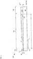
- FIG. 1 depicts a schematic drawing of a side view of a ramp formed via an exemplary accelerator-layer tapering process.
- Substrate region 100 includes regions 102, 104, and 106, each of which includes substrate 108 and layer 110. Region 104 extends from first end 112, where it abuts region 102, to second end 114, where it abuts region 106.
- FIGS. 2A-C depict schematic drawings of side views of a substrate region comprising a tapered region at different points during an exemplary accelerator-layer tapering process.
- FIG. 3 depicts operations of an exemplary one-dimensional accelerator-layer tapering process.
- FIG. 3 is described with continuing reference to FIGS. 1 and 2A-C .
- Method 300 begins with operation 301, wherein accelerator layer 202 is formed on surface 206 of layer 110.
- Layer 110 is a planar layer of stoichiometric silicon nitride having a thickness, h1.
- layer 110 comprises silicon nitride in this example
- the accelerator-layer tapering process is suitable for tapering any layer of material whose structure does not inhibit substantially uniform etch rate in all dimensions.
- Materials for which an accelerator-layer tapering process is suitable include, without limitation, dielectrics, silicon oxides, glasses, plastics, ceramics, silicon, polysilicon, amorphous silicon, amorphous and polycrystalline silicon-containing compounds ( e.g ., silicon carbide, etc .), crystalline III-V compound semiconductors, polycrystalline III-V compound semiconductors, amorphous III-V compound semiconductors, crystalline II-VI compound semiconductors, polycrystalline II-VI compound semiconductors, amorphous II-VI compound semiconductors, metals, and composite materials.
- Accelerator layer 202 comprises a sacrificial material that etches in a first etchant that also etches the material of layer 110.
- the material of accelerator layer 202 is selected such that it etches at a faster rate in the first etchant than the material of layer 110 .
- the material of accelerator layer 202 is a matter of design choice and will depend on the material of layer 110 and available etchants.
- mask layer 204 is formed and patterned on accelerator layer 202.
- Mask layer 204 is patterned to expose surface 208 of accelerator layer 202 in region 102, but initially protect surface 208 in regions 104 and 106.
- FIG. 2A depicts a cross-sectional view of substrate region 100 after the formation of mask layer 204 on accelerator layer 202.
- substrate region 100 is exposed to etchant 210 at time t(0).
- Etchant 210 comprises a chemical (e.g ., nitric acid, etc .) that etches the material of accelerator layer 202 at a faster rate than the material of layer 110. As a result, accelerator layer 202 is removed quickly in region 102 and etchant 210 begins to attack underlying layer 110 uniformly across the region. At the same time, etchant 210 begins to etch accelerator layer 202 laterally along the z-direction from first end 112 toward second end 114, undercutting mask layer 204 along the z-direction. In some embodiments, accelerator layer 202 is removed from region 102 via a different etch (preferably, a directional etch) that removes its material selectively over the material of layer 110. This ensures a clean starting condition at first end 112 for the lateral etching of accelerator layer 202 in region 104. It can also improve the uniformity of the vertical etching of layer 110 in region 102.
- a chemical e.g ., nitric acid, etc
- FIG. 2B depicts a cross-sectional view of substrate region 100 during operation 303.
- Etch front 212 moves along the z-direction at a substantially constant velocity, thus exposing a linearly increasing amount of surface 206.
- Time t(1) is selected based on the etch rate of the material of layer 110 in etchant 210, initial thickness, h1, final thickness, h2, and the desired length, L1, of taper region 104.
- Second end 114 is defined by the point at which etch front 212 is stopped in operation 204. As a result, no etching of layer 110 occurs at second end 114 (or beyond it in region 106) because etchant 210 has no time to attack layer 110 at surface 206. At second end 114 and in region 106, therefore, layer 110 remains at its deposited thickness, hi. At first end 112 and in region 102, however, etchant 210 etches layer 110 for substantially the entire time period from t(0) to t(1), resulting in final thickness, h2, for layer 110. Between first end 112 and second end 114, the exposure time of layer 110 in etchant 210 is a linearly decreasing function of distance along the z-direction from first end 112.
- Etchant 210 therefore, creates a linearly increasing thickness of layer 110 (from h2 to hi) from first end 112 to second end 114.
- the magnitude of the taper angle, ⁇ 1 is dependent upon the relative etch rates of the materials of accelerator layer 202 and layer 110 in etchant 210.
- each etch rate can vary for the same material depending on how that material was formed (e.g ., deposition temperature, annealing temperature, annealing time, etc. ).
- FIG. 2C depicts a cross-sectional view of substrate region 100 after operation 304.
- accelerator-layer tapering can be implemented so as to form regions having tapers that are mutually non-orthogonal (e.g ., a beveled region or wedge), as well as, by judicious design of mask features, taper regions having non-linear tapers.
- FIGS. 4A and 4B depict schematic drawings of top and side views, respectively, of a surface waveguide core of a spotsize converter having a double-angle taper thickness profile.
- Surface waveguide core 400 comprises low-contrast region 402, taper region 404, and high-contrast region 406.
- Low-contrast region 402, taper region 404, and high-contrast region 406 are formed in core layer 408 using accelerator-layer tapering, as described above.
- Core layer 408 is disposed on conventional lower cladding 410.
- Taper region 404 includes first taper region 412 and second taper region 414, each of which has a different taper angle.
- surface waveguide core 400 is a ridge of stoichiometric silicon nitride having a substantially rectangular cross-sectional shape having a thickness that is typically within the range of a few nm to approximately 300 nm and a width that is typically within the range of a few nm to tens of microns.
- core 400 has a different shape, such as square, irregular ( e.g., a "u" shape, "T” shape, etc. ).
- FIG. 4 depicts surface waveguide core 400 after its thickness has been tapered but prior to the removal of mask layer 418 and accelerator layer 416. Waveguide core 400 is also depicted prior to its lateral definition.
- mask layer 418 is first formed on the surface of accelerator layer 416 and patterned to define opening 420, wedge 422, and field region 424. Opening 420 defines low-contrast region 402. Each of the sides of wedge 422 form angle ⁇ 1 relative to line 426 and ⁇ 2 relative to propagation axis 428. Line 426 is a line normal to optical propagation axis 428, as shown. Field region 424 protects second taper region 414 and high-contrast region 406 in the same manner as is described above and with respect to one-dimensional accelerator-layer tapering.
- Wedge 422 protects core layer 408 and accelerator layer 416 from vertical attack during the taper etch that forms taper region 404; however, accelerator layer 416 enables accelerator-layer etching of the core layer to proceed along three directions - the z-direction, direction 432, and direction 434, as shown. As a result, accelerator layer 416 is etched laterally at a faster rate in first taper region 412 than in second taper region 414, resulting in a more gradual tapering of core layer 408 in first taper region 412 than in second taper region 414. Iso-height profiles 430 indicate vertical height changes of 10 nm.
- first taper region 412 defines a substantially linear slope having an angle ⁇ 2 with respect to the original top surface of core layer 408, while the more rapid height change in second taper region 414 defines a substantially linear slope having an angle ⁇ 3 with respect to the original top surface of core layer 408.
- Boundary 436 denotes an approximate transition between first taper region 412 and second taper region 414.
- Boundary 438 denotes an approximate transition between second taper region 414 and high-contrast region 406.
- ⁇ 3 depend on the relative etch rates of accelerator layer 416 and core layer 408, as described above and with respect to ⁇ 1 of FIG. 2C .
- FIG. 5A depicts a plot of taper profile for an exemplary spotsize converter having a double-angle taper region.
- Plot 500 shows the thickness of a taper region of a core layer formed using a wedge 422 having angle ⁇ 1 of approximately 85°. As cos(85°) is approximately 1/10, the angles ⁇ 2 and ⁇ 3 have this ratio. -. In taper region 412, taper angle ⁇ 2 is approximately 0.001°, while in taper region 414, taper angle ⁇ 3 is approximately 0.010°.
- Boundary 436 denotes the approximate transition between angles ⁇ 2 and ⁇ 3 .
- FIGS. 5B and 5C depict plots of a mode profile angles induced by an exemplary double-angle taper region and a single-angle linear taper region, respectively.
- Plot 508 shows the mode profile angle, ⁇ , induced by the taper angle of a double-angle linear taper having taper angles ⁇ 2 and ⁇ 3 of 0.001° and 0.010°, respectively for TE polarized light at 1550 nm.
- plot 512 shows the mode profile angle, ⁇ , induced by the taper angle of a simple linear taper for TE polarized light at 1550 nm.
- a comparison of plots 508 and 512 shows that the angle of the mode profile induced by the double-angle taper region is improved over that of the simple linear taper region.
- the techniques used to define the double-angle taper described above can also be used to define a taper having a non-linear, relatively complex vertical profile, such as a ramp having a steadily curving or substantially sinusoidal profile.
- Such layers can be advantageously used in the core and/or cladding layers of a transition region of a spot-size converter, as they can facilitate an adiabatic transition from one guided-mode profile to another.
- FIGS. 6A-B depict schematic drawings of side and top views, respectively, of a spotsize converter having a substantially sinusoidally tapered core layer in accordance with an illustrative embodiment of the present invention.
- Spotsize converter 600 comprises low-contrast region 602, taper region 604, and high-contrast region 606.
- spotsize converter 600 includes a waveguide structure comprising lower cladding 608, core layer 610, and upper cladding 612.
- the thickness of core layer 610 varies, from h3 at first end 614 to h4 at second end 616, as a substantially sinusoidal function of position along the z-direction within taper region 604, as described below.
- Low-contrast region 602 and taper region 604 are formed by tapering core layer 608 using accelerator-layer tapering, as described above.
- FIG. 7 depicts operations of a method suitable for forming a spotsize converter in accordance with the illustrative embodiment.
- Method 700 begins with operation 701, wherein core layer 610 is formed on lower cladding 608.
- FIGS. 8A-D depict schematic drawings of views of spotsize converter 600 at different points in its fabrication.
- Lower cladding 608 is a conventional lower cladding layer having a thickness and refractive index suitable for use with core layer 608.
- lower cladding 608 is a layer of thermally grown silicon dioxide having a thickness within the range of 5 microns to 50 microns, and preferably 15 microns. It will be clear to one skilled in the art that the material and thickness of lower cladding 608 are matters of design and that any practical thickness and/or material can be used.
- Core layer 610 is a layer of stoichiometric silicon nitride having a thickness, h3, within the range of approximately 50 nm to approximately 300 nm. In the illustrative embodiment, core layer 610 has a thickness of approximately 220 nm. Typically, core layer 610 is grown on lower cladding 608 using Low-Pressure Chemical Vapor Deposition (LPCVD); however, one skilled in the art will recognize that any suitable method can be used to form core layer 610.
- LPCVD Low-Pressure Chemical Vapor Deposition
- accelerator layer 802 is formed on surface 806 of core layer 610.
- mask layer 804 is formed on surface 808 of accelerator layer 802 and patterned to define opening 810, shaped region 812, and field region 814.
- FIGS. 8A-B depict schematic drawings of top and side views, respectively, of nascent spotsize converter 600 after formation of mask layer 804.
- FIG. 8B depicts a cross-sectional view through line a-a of FIG. 8A , as indicated.
- Opening 810 defines the area of core layer 610 in which low-contrast region 602 is defined. Opening 810 includes sides 816 and 818 that extend from tip 824 to end 826, where shaped region 812 abuts field region 814. Sides 816 and 818 define the width, ⁇ (z), of shaped region 812, which typically increases monotonically from tip 824 to end 826. Each of sides 816 and 818 has a shape that gives rise to a desired thickness taper profile for core layer 610 in transition region 604. The shape of sides 816 and 818 is calculated from the desired vertical profile of transition region 804.
- each of sides 816 and 818 forms an instantaneous angle ⁇ relative to line 822, which is a line drawn normal to propagation axis 820 at that point (i.e., the line aligned with the x-direction at the given z, as shown).
- This instantaneous angle defines the shape of opening 810.
- FIG. 9 depicts operations of a method suitable for determining the shape of opening 810 in accordance with the illustrative embodiment of the present invention.
- Method 900 begins with operation 901, wherein the desired mode-field profile of a light signal in low-contrast region 602 is determined.
- the mode-field profile is defined by the mode-field diameters in both the x- and y-directions for each polarization of the light signals ( e.g. , TE and TM, right- and left-hand circular, etc .).
- the mode-field profile in a surface waveguide is based on several factors, including the materials of the core and cladding of the waveguide, the vertical and lateral dimension (i.e., width) of the waveguide, and the wavelength of the light.
- the desired mode-field profile of the light signal in high-contrast region 606 is determined.
- an estimate of a desired thickness profile, h(z), is determined for core layer 610 in transition region 604.
- the desired thickness profile, h(z) is other than a sine-bend shape ( e.g ., an exponential function, etc .).
- the desired thickness profile in transition region 604 is based on the application for which spotsize converter 600 is intended.
- a spline interpolation is performed to determine a smooth interpolation between the mode-field profiles in the low-contrast and high-contrast regions.
- the mode-field profile in transition region 604 can be described by a numerical function MFD(h(z)).
- MFD(h) is calculated for several intermediate thicknesses along transition region 604 such that the spline interpolation provides an MFD(h) that is a substantially smooth numerical function.
- a mode-profile-angle function ⁇ (z) suitable for generating the result of the spline interpolation is calculated based on MFD(h(z)) and Equations (1) and (2) above, as well as the length, L2, of transition region 604. It should be noted that the mode-profile angle ⁇ indicates the rate at which the mode profile changes along the z-direction.
- taper-angle function ⁇ (z) is calculated so as to give rise to the desired mode-profile-angle function ⁇ (z) .
- the instantaneous taper-angle ⁇ is defined as the angle formed, at any given z, between the tangent to the top surface of core layer 610 and a line parallel to a horizontal plane ( e.g., the top surface of lower cladding 608, as shown in FIG. 8D ).
- etch-front-angle function ⁇ (z) is defined for each of sides 816 or 818 so as to give rise to taper-angle function ⁇ (z).
- Etch-front-angle function ⁇ (z) dictates the etch-front angle at each point on sides 816 and 818 for each point z along shaped region 812.
- the term "etch-front angle” is defined as the magnitude of the angle formed between a line drawn normal to the propagation axis at a point z and a line drawn tangent to a side of a shaped region at that z.
- Etch-front-angle function ⁇ (z) determines the magnitude of the distance between each of sides 816 and 818 and propagation axis 820 ( i.e., the width of shaped region 812) from tip 824 to end 826.
- opening 810 is defined such that sides 816 and 818 are characterized by etch-front-angle function ⁇ (z).
- FIGS. 10A-B depict plots of the magnitude of etch-front angle ⁇ as a function of distance, z, for taper regions having lengths of 2 mm and 1 mm, respectively.
- nascent spotsize converter 600 is exposed to a suitable etchant (e.g ., etchant 210) at time t(0).
- a suitable etchant e.g ., etchant 210
- the etchant is selected such that it etches the material of accelerator layer 802 at a faster rate than the material of core layer 610.
- accelerator layer 802 is removed quickly in region 602 and the etchant begins to etch the accelerator layer laterally along the z-direction, as well as along directions normal to sides 816 and 818, thereby undercutting mask layer 804.
- the etch fronts from each exposed edge of shaped region 812 begin to meet. Since the lateral extent of shaped region 812 is a function of z, the duration of the exposure of surface 806 to the etchant is a function of both ⁇ (z) and z. As a result, the thickness of core layer 610 in shaped region 812 is based on t, ⁇ (z), and z. Along the z-direction, therefore, the profile of core layer 610 can be selected as nearly any desired monotonically increasing function of z, by judicious selection of ⁇ (z).
- this profile is substantially a portion of a sinusoid; however, it will be clear to one skilled in the art, after reading this Specification, how to specify, make, and use tapered regions having any suitable substantially monotonically changing vertical profile, including linear, piecewise linear, non-linear, sinusoidal, curved, irregular, and the like.
- Time t(1) is selected based on the etch rate of the material of layer 110 in etchant 210, initial thickness, h3, final thickness, h4, and the desired length, L2, of taper region 604.
- FIGS. 8C and 8D depict top and side views, respectively, of nascent spotsize converter 600 after the tapering of core layer 610.
- iso-height lines 828 indicate height changes of approximately 20 nm.
- FIGS. 11A-B depict plots of the thickness of exemplary core layers 610 as a function of distance, z, for taper regions having lengths of 2 mm and 1 mm, respectively.
- Plots 1100 and 1102 show the thickness of core layer 610 from second end 616 to first end 614, for a core layer having an initial thickness, h3, of 220 nm and a final thickness, h4, in low-contrast region 602 of approximately 65 nm.
- FIGS. 11C-D depict plots of the taper angle, ⁇ , of exemplary core layers 610 as a function of distance, z, for taper regions having lengths of 2 mm and 1 mm, respectively.
- Plots 1104 and 1106 show the instantaneous angle of the top surface of core layer 610 from second end 616 to first end 614, for a core layer having an initial thickness, h3, of 220 nm and a final thickness, h4, in low-contrast region 602 of approximately 65 nm.
- accelerator layer 802 and mask layer 804 are stripped from nascent spotsize converter 600.
- core layer 610 is patterned to define core 618.
- core 618 has width w1, which is within the range of a few nanometers to a few tens of microns and typically about 1 micron.
- core 618 has width w2, which is also within the range of a few nanometers to a few tens of microns.
- w1 is approximately 1 micron and w2 is approximately 65 nm.
- the width of core 618 is a function of z. In some embodiments, the width function w(z) is determined in analogous fashion to that described above and with respect to FIG. 9 .
- w(z) changes monotonically along transition region 604.
- transition region 604 has a thickness that approximates a sine-bend shape
- core 618 has the same width in all of regions 602, 604, and 606.
- core 618 comprises a composite core having an inner core of a first material (e.g ., silicon dioxide) surrounded by an outer core of a second material (e.g ., silicon nitride).
- core 618 comprises a composite core having a central core of a first material (e.g ., silicon dioxide) that is disposed between lower and upper core layers comprising a second material (e.g., silicon nitride).
- a composite core is characterized by an effective refractive index that is determined by the materials used as well as the geometry of the core design. As a result, these factors also affect the effective refractive-index contrast of a composite-core waveguide, which is also affected by other factors, such as core and cladding dimensions, core and cladding materials, and the like.
- the transition region wherein the lateral dimension of core 618 changes is not aligned along the z-direction with the transition region wherein the thickness of core 618 changes.
- spotsize converter 600 includes two separate transition regions - one for the thickness of core 618 and another for the lateral dimension of core 618.
- upper cladding 612 is formed on core layer 610 in conventional fashion to complete the fabrication of spotsize converter 600.
- Upper cladding 612 is normally a layer of silicon oxide (e.g ., silicon dioxide, silicon monoxide, etc. ) formed via LPCVD deposition using a precursor gas such as tetraethyl orthosilicate (TEOS), which results in a conformal oxide layer.
- silicon oxide e.g ., silicon dioxide, silicon monoxide, etc.
- TEOS tetraethyl orthosilicate
- Upper cladding 612 typically has a thickness within the range of approximately 1 micron to approximately 30 microns. In the illustrative embodiment, upper cladding has a thickness of approximately 15 microns. In some embodiments, upper cladding 612 has a thickness that is less than 1 micron. In some embodiments, upper cladding 612 is not present.
- the illustrative embodiment includes a waveguide having lower and upper cladding layers that have substantially uniform thickness throughout
- at least one of the upper and lower cladding layers is tapered in similar fashion to the manner in which core layer 610 is tapered, as described above, such that one or both of these cladding layers has a thickness and/or width that changes along the propagation direction in at least a portion of a waveguide.
- FIGS. 12A and 12B depict plots of a mode profile induced by exemplary sinusoidal taper regions having lengths of approximately 2 mm and 1 mm, respectively.
- Plot 1200 shows the mode profile angle, ⁇ , along transition region 604 from second end 616 to first end 614, where the length of the transition region, L2, is 2 mm.
- Traces 1202 and 1204 show the mode profile angle for TE and TM polarized light, respectively, at 1550 nm.
- Plot 1206 shows the mode profile angle, ⁇ , along transition region 604 from second end 616 to first end 614, where the length of the transition region, L2, is 1 mm.
- Traces 1208 and 1210 show the mode profile angle for TE and TM polarized light, respectively, at 1550 nm.
- the illustrative embodiment comprises a spotsize converter having a transition region including a core layer having a sinusoidal thickness profile
- a spotsize converter having a transition region including a core layer having a sinusoidal thickness profile it will be clear to one skilled in the art, after reading this Specification, how to specify, make, and use spotsize converters that include a core layer having any suitable substantially changing vertical profile, including linear, piecewise linear, non-linear, curved, irregular, monotonically changing, non-monotonically changing, exponential, and the like.
- core layer 610 is formed such that it has a taper angle that changes in substantially constant fashion along transition region 604 (neglecting changes that might occur in the immediate vicinity of first end 614 or second end 616 ).
- a thickness profile affords these embodiments with additional advantages, such as the ability to distribute vertical bending loss (induced by peaks in the taper angle) evenly along the length of the transition region.
- core layer 610 is formed as part of a waveguide structure such that the value of the mode-profile-angle, ⁇ , of the waveguide remains substantially constant along the length of transition region 604. In some of these embodiments, the thickness of core layer 610 increases substantially exponentially along the length of transition region 604.
Landscapes
- Physics & Mathematics (AREA)
- Engineering & Computer Science (AREA)
- Microelectronics & Electronic Packaging (AREA)
- General Physics & Mathematics (AREA)
- Optics & Photonics (AREA)
- Power Engineering (AREA)
- Optical Integrated Circuits (AREA)
Claims (6)
- Verfahren, das Folgendes umfasst:Bereitstellen eines Substrats (608) mit einer ersten Region (602), einer zweiten Region (606) und einer dritten Region (604), die zwischen der ersten Region und der zweiten Region liegt, wobei die dritte Region an einer ersten Stelle (616) entlang einer ersten Achse (z) an der zweiten Region anstößt und wobei die dritte Region an einer zweiten Stelle (614) entlang der ersten Achse an der zweiten Region anstößt; undBereitstellen einer ersten Schicht (610) eines auf dem Substrat angeordneten ersten Materials, wobei die erste Schicht in der ersten Region eine erste Dicke (h4) und in der zweiten Region eine zweite Dicke (h3) aufweist, und wobei sich die Dicke (h(z)) der ersten Schicht in der dritten Region auf nichtlineare Weise von der ersten Dicke an der ersten Stelle zu der zweiten Dicke an der zweiten Stelle ändert, und wobei die erste Schicht durch Vorgänge bereitgestellt wird, die Folgendes umfassen:(i) Bilden der ersten Schicht mit einer ersten Oberfläche (806) und einer Dicke, die gleich der zweiten Dicke ist;(ii) Bilden einer Beschleunigerschicht (802) auf der ersten Oberfläche, wobei die Schicht ein zweites Material und eine zweite Oberfläche (808) umfasst;(iii) Bilden einer Abdeckschicht (804) auf der zweiten Oberfläche, wobei die Abdeckschicht eine Öffnung (810) definiert, die eine erste Seite (816) und eine zweite Seite (818) aufweist, die eine geformte Region definieren, die eine erste Breite Δ(z) aufweist, die monoton und nichtlinear zwischen der ersten Stelle und der zweiten Stelle zunimmt, wobei die Form der ersten Seite und der zweiten Seite jeweils von einer Ätzfront-Winkelfunktion (Φ(z)) gekennzeichnet ist, die auf einem ersten gewünschten Dickenprofil (h(z)) für die erste Schicht in der dritten Region basiert; und(iv) Ätzen der ersten Schicht (610) und der Beschleunigerschicht (802) in einem ersten Ätzmittel (210) während eines ersten Zeitraums (t1), wobei das erste Ätzmittel derart ausgewählt wird, dass es das zweite Material mit einer höheren Geschwindigkeit ätzt als das erste Material, wobei der erste Zeitraum basierend auf der Ätzgeschwindigkeit des ersten Materials, der ersten Dicke (h4), der zweiten Dicke (h3) und dem Abstand (L2) zwischen der ersten Stelle und der zweiten Stelle ausgewählt wird.
- Verfahren nach Anspruch 1, wobei die erste Schicht (610) und die Beschleunigerschicht (802) derart geätzt werden, dass die Beschleunigerschicht mittels des ersten Ätzmittels in Querrichtung von der ersten Stelle (616) zu der zweiten Stelle (614) geätzt wird, und derart, dass die erste Schicht an der ersten Stelle dem ersten Ätzmittel während des ersten Zeitraums ausgesetzt wird und derart, dass die erste Schicht an der zweiten Stelle dem ersten Ätzmittel im Wesentlichen nicht ausgesetzt wird.
- Verfahren nach Anspruch 1, das weiter Folgendes umfasst:(v) Bereitstellen einer zweiten Schicht (608), umfassend ein drittes Material mit einem Brechungsindex, der geringer ist als der Brechungsindex des ersten Materials, wobei die erste Schicht auf der zweiten Schicht angeordnet ist; und(vi) Bereitstellen einer dritten Schicht (612), umfassend ein viertes Material mit einem Brechungsindex, der geringer ist als der Brechungsindex des ersten Materials, wobei die dritte Schicht auf der ersten Schicht angeordnet ist;wobei die erste Schicht, die zweite Schicht und die dritte Schicht kollektiv einen Oberflächenwellenleiter (600) definieren, der in der ersten Region (602) ein erstes Modenfeldprofil für ein Lichtsignal und in der zweiten Region (606) ein zweites Modenfeldprofil für das Lichtsignal aufweist, und wobei sich das Modenfeldprofil auf nichtlineare Weise entlang der Länge der dritten Region (604) von dem ersten Modenfeldprofil zu dem zweiten Modenfeldprofil ändert.
- Verfahren nach Anspruch 3, wobei die Abdeckschicht durch Vorgänge bereitgestellt wird, die Folgendes umfassen:(a) Bestimmen des ersten Modenfeldprofils und des zweiten Modenfeldprofils;(b) Schätzen des ersten gewünschten Dickenprofils (h(z)) für die erste Schicht (610) in der dritten Region (604);(c) Ausführen einer Spline-Interpolation zwischen dem ersten Modenfeldprofil und dem zweiten Modenfeldprofil, wobei die Spline-Interpolation auf dem geschätzten gewünschten Dickenprofil basiert;(d) Bestimmen einer Modenprofil-Winkelfunktion (ψ(z)) basierend auf der Spline-Interpolation;(e) Bestimmen der Verjüngungswinkelfunktion (θ(z)) basierend auf der Modenprofil-Winkelfunktion; und(f) Bestimmen der Ätzfront-Winkelfunktion (Φ(z)) basierend auf der Verjüngungswinkelfunktion.
- Verfahren nach Anspruch 1, das weiter Folgendes umfasst:(v) Bereitstellen einer zweiten Schicht (608), umfassend ein zweites Material, wobei die erste Schicht auf der zweiten Schicht angeordnet ist; und(vi) Bereitstellen einer dritten Schicht (612), umfassend ein drittes Material, wobei die dritte Schicht auf der ersten Schicht angeordnet ist;wobei die erste Schicht, die zweite Schicht und die dritte Schicht kollektiv einen Oberflächenwellenleiter (600) definieren, und wobei der Oberflächenwellenleiter in der ersten Region ein erstes Modenprofil für ein Lichtsignal und in der zweiten Region ein zweites Modenprofil für das Lichtsignal aufweist, und wobei weiter das Modenprofil entlang der Länge der dritten Region adiabatisch zwischen dem ersten Modenprofil und dem zweiten Modenprofil übergeht.
- Verfahren nach Anspruch 5, wobei der Oberflächenwellenleiter (600) durch einen ersten Kontrast der effektiven Brechungsindizes in der ersten Region (602) und einen zweiten Kontrast der effektiven Brechungsindizes in der zweiten Region (606) gekennzeichnet ist, und wobei sich der Kontrast der effektiven Brechungsindizes entlang der Länge der dritten Region (604) zwischen dem ersten Kontrast der effektiven Brechungsindizes und dem zweiten Kontrast der effektiven Brechungsindizes ändert.
Applications Claiming Priority (1)
| Application Number | Priority Date | Filing Date | Title |
|---|---|---|---|
| US14/270,014 US9268089B2 (en) | 2011-04-21 | 2014-05-05 | Layer having a non-linear taper and method of fabrication |
Publications (2)
| Publication Number | Publication Date |
|---|---|
| EP2942652A1 EP2942652A1 (de) | 2015-11-11 |
| EP2942652B1 true EP2942652B1 (de) | 2018-10-10 |
Family
ID=51212666
Family Applications (1)
| Application Number | Title | Priority Date | Filing Date |
|---|---|---|---|
| EP14175029.9A Active EP2942652B1 (de) | 2014-05-05 | 2014-06-30 | Abgeschrägte Schicht mit nichtlinearer Dickenänderung und Herstellungsverfahren |
Country Status (2)
| Country | Link |
|---|---|
| EP (1) | EP2942652B1 (de) |
| KR (1) | KR102057740B1 (de) |
Citations (1)
| Publication number | Priority date | Publication date | Assignee | Title |
|---|---|---|---|---|
| JP3112115B2 (ja) * | 1992-03-13 | 2000-11-27 | 日本電信電話株式会社 | 光導波路の製造方法 |
Family Cites Families (7)
| Publication number | Priority date | Publication date | Assignee | Title |
|---|---|---|---|---|
| US4865407A (en) * | 1987-10-22 | 1989-09-12 | Brother Kogyo Kabushiki Kaisha | Optical waveguide element, method of making the same and optical coupler employing optical waveguide element |
| US5208882A (en) * | 1991-11-14 | 1993-05-04 | Eastman Kodak Company | Hybrid thin film optical waveguide structure having a grating coupler and a tapered waveguide film |
| US20020191916A1 (en) * | 2001-06-15 | 2002-12-19 | Confluent Photonics, Corporation | Vertical waveguide tapers for optical coupling between optical fibers and thin silicon waveguides |
| KR20070091288A (ko) * | 2004-11-17 | 2007-09-10 | 컬러 칩 (이스라엘) 리미티드. | 도파로 테이퍼링 및 최적화된 도파로 구조물 형성의프로세스 및 방법 |
| WO2009051562A1 (en) * | 2007-10-18 | 2009-04-23 | Agency For Science, Technology And Research | An optical coupling device and a method of optically coupling light |
| US8718432B1 (en) * | 2011-04-21 | 2014-05-06 | Octrolix Bv | Method for forming a spotsize converter |
| US9020317B2 (en) * | 2012-10-11 | 2015-04-28 | Octrolix Bv | Surface waveguide having a tapered region and method of forming |
-
2014
- 2014-06-30 EP EP14175029.9A patent/EP2942652B1/de active Active
- 2014-07-08 KR KR1020140085068A patent/KR102057740B1/ko active Active
Patent Citations (1)
| Publication number | Priority date | Publication date | Assignee | Title |
|---|---|---|---|---|
| JP3112115B2 (ja) * | 1992-03-13 | 2000-11-27 | 日本電信電話株式会社 | 光導波路の製造方法 |
Also Published As
| Publication number | Publication date |
|---|---|
| EP2942652A1 (de) | 2015-11-11 |
| KR20150126763A (ko) | 2015-11-13 |
| KR102057740B1 (ko) | 2019-12-19 |
Similar Documents
| Publication | Publication Date | Title |
|---|---|---|
| US9939582B2 (en) | Layer having a non-linear taper and method of fabrication | |
| US8718432B1 (en) | Method for forming a spotsize converter | |
| US7103245B2 (en) | High density integrated optical chip | |
| EP2720073B1 (de) | Oberflächenwellenleiter mit konischem Bereich und Verfahren zur Herstellung | |
| US6870987B2 (en) | Embedded mode converter | |
| Song et al. | Low-loss waveguide bends by advanced shape for photonic integrated circuits | |
| CA2734614C (en) | Optical mode transformer, in particular for coupling an optical fiber and a high-index contrast waveguide | |
| US6571039B1 (en) | Optical waveguide having a weakly-confining waveguide section and a strongly-confining waveguide section optically coupled by a tapered neck | |
| US9417388B2 (en) | Spot-size conversion optical waveguide | |
| EP2634613B1 (de) | Optische Vorrichtung, optischer Sender, optischer Empfänger, optischer Sendeempfänger und Verfahren zur Herstellung der optischen Vorrichtung | |
| KR101121459B1 (ko) | 광섬유 및 평면 광학 도파관을 치밀하게 결합하는 방법 및장치 | |
| JP4377195B2 (ja) | 光モジュールの製造方法 | |
| EP2942652B1 (de) | Abgeschrägte Schicht mit nichtlinearer Dickenänderung und Herstellungsverfahren | |
| Wang et al. | Experimental realization of a low-loss nano-scale Si hybrid plasmonic waveguide | |
| JP2001221926A (ja) | 光導波路素子の製造方法 | |
| WO2004008203A1 (en) | Planar waveguide with tapered region | |
| US20240369763A1 (en) | 3d tapered nanophotonic waveguide to fiber edge coupler | |
| JP4313772B2 (ja) | 光導波路の製造方法 | |
| RU2712985C1 (ru) | Устройство модового конвертера | |
| Solehmainen | Fabrication of microphotonic waveguide components on silicon | |
| CA2578541A1 (en) | Interface device for performing mode transformation in optical waveguides | |
| WO2018150899A1 (ja) | 光導波路素子および光導波路素子の製造方法 | |
| Ku et al. | Metal-Insulator-Silicon-Insulator-Metal Waveguide with Its Insulator Replaced by Fluid | |
| Horth | Constant-loss taper and low-index waveguide for silicon photonics applications |
Legal Events
| Date | Code | Title | Description |
|---|---|---|---|
| PUAI | Public reference made under article 153(3) epc to a published international application that has entered the european phase |
Free format text: ORIGINAL CODE: 0009012 |
|
| AK | Designated contracting states |
Kind code of ref document: A1 Designated state(s): AL AT BE BG CH CY CZ DE DK EE ES FI FR GB GR HR HU IE IS IT LI LT LU LV MC MK MT NL NO PL PT RO RS SE SI SK SM TR |
|
| AX | Request for extension of the european patent |
Extension state: BA ME |
|
| 17P | Request for examination filed |
Effective date: 20160510 |
|
| RBV | Designated contracting states (corrected) |
Designated state(s): AL AT BE BG CH CY CZ DE DK EE ES FI FR GB GR HR HU IE IS IT LI LT LU LV MC MK MT NL NO PL PT RO RS SE SI SK SM TR |
|
| STAA | Information on the status of an ep patent application or granted ep patent |
Free format text: STATUS: EXAMINATION IS IN PROGRESS |
|
| 17Q | First examination report despatched |
Effective date: 20170308 |
|
| RAP1 | Party data changed (applicant data changed or rights of an application transferred) |
Owner name: LIONIX INTERNATIONAL BV |
|
| RAP1 | Party data changed (applicant data changed or rights of an application transferred) |
Owner name: LIONIX INTERNATIONAL B.V. |
|
| GRAP | Despatch of communication of intention to grant a patent |
Free format text: ORIGINAL CODE: EPIDOSNIGR1 |
|
| STAA | Information on the status of an ep patent application or granted ep patent |
Free format text: STATUS: GRANT OF PATENT IS INTENDED |
|
| INTG | Intention to grant announced |
Effective date: 20180430 |
|
| GRAS | Grant fee paid |
Free format text: ORIGINAL CODE: EPIDOSNIGR3 |
|
| GRAA | (expected) grant |
Free format text: ORIGINAL CODE: 0009210 |
|
| STAA | Information on the status of an ep patent application or granted ep patent |
Free format text: STATUS: THE PATENT HAS BEEN GRANTED |
|
| AK | Designated contracting states |
Kind code of ref document: B1 Designated state(s): AL AT BE BG CH CY CZ DE DK EE ES FI FR GB GR HR HU IE IS IT LI LT LU LV MC MK MT NL NO PL PT RO RS SE SI SK SM TR |
|
| REG | Reference to a national code |
Ref country code: GB Ref legal event code: FG4D |
|
| REG | Reference to a national code |
Ref country code: CH Ref legal event code: EP Ref country code: AT Ref legal event code: REF Ref document number: 1051908 Country of ref document: AT Kind code of ref document: T Effective date: 20181015 |
|
| REG | Reference to a national code |
Ref country code: IE Ref legal event code: FG4D |
|
| REG | Reference to a national code |
Ref country code: DE Ref legal event code: R096 Ref document number: 602014033675 Country of ref document: DE |
|
| REG | Reference to a national code |
Ref country code: NL Ref legal event code: FP |
|
| REG | Reference to a national code |
Ref country code: LT Ref legal event code: MG4D |
|
| REG | Reference to a national code |
Ref country code: AT Ref legal event code: MK05 Ref document number: 1051908 Country of ref document: AT Kind code of ref document: T Effective date: 20181010 |
|
| PG25 | Lapsed in a contracting state [announced via postgrant information from national office to epo] |
Ref country code: ES Free format text: LAPSE BECAUSE OF FAILURE TO SUBMIT A TRANSLATION OF THE DESCRIPTION OR TO PAY THE FEE WITHIN THE PRESCRIBED TIME-LIMIT Effective date: 20181010 Ref country code: LT Free format text: LAPSE BECAUSE OF FAILURE TO SUBMIT A TRANSLATION OF THE DESCRIPTION OR TO PAY THE FEE WITHIN THE PRESCRIBED TIME-LIMIT Effective date: 20181010 Ref country code: NO Free format text: LAPSE BECAUSE OF FAILURE TO SUBMIT A TRANSLATION OF THE DESCRIPTION OR TO PAY THE FEE WITHIN THE PRESCRIBED TIME-LIMIT Effective date: 20190110 Ref country code: AT Free format text: LAPSE BECAUSE OF FAILURE TO SUBMIT A TRANSLATION OF THE DESCRIPTION OR TO PAY THE FEE WITHIN THE PRESCRIBED TIME-LIMIT Effective date: 20181010 Ref country code: IS Free format text: LAPSE BECAUSE OF FAILURE TO SUBMIT A TRANSLATION OF THE DESCRIPTION OR TO PAY THE FEE WITHIN THE PRESCRIBED TIME-LIMIT Effective date: 20190210 Ref country code: FI Free format text: LAPSE BECAUSE OF FAILURE TO SUBMIT A TRANSLATION OF THE DESCRIPTION OR TO PAY THE FEE WITHIN THE PRESCRIBED TIME-LIMIT Effective date: 20181010 Ref country code: BG Free format text: LAPSE BECAUSE OF FAILURE TO SUBMIT A TRANSLATION OF THE DESCRIPTION OR TO PAY THE FEE WITHIN THE PRESCRIBED TIME-LIMIT Effective date: 20190110 Ref country code: PL Free format text: LAPSE BECAUSE OF FAILURE TO SUBMIT A TRANSLATION OF THE DESCRIPTION OR TO PAY THE FEE WITHIN THE PRESCRIBED TIME-LIMIT Effective date: 20181010 Ref country code: HR Free format text: LAPSE BECAUSE OF FAILURE TO SUBMIT A TRANSLATION OF THE DESCRIPTION OR TO PAY THE FEE WITHIN THE PRESCRIBED TIME-LIMIT Effective date: 20181010 Ref country code: LV Free format text: LAPSE BECAUSE OF FAILURE TO SUBMIT A TRANSLATION OF THE DESCRIPTION OR TO PAY THE FEE WITHIN THE PRESCRIBED TIME-LIMIT Effective date: 20181010 |
|
| PG25 | Lapsed in a contracting state [announced via postgrant information from national office to epo] |
Ref country code: RS Free format text: LAPSE BECAUSE OF FAILURE TO SUBMIT A TRANSLATION OF THE DESCRIPTION OR TO PAY THE FEE WITHIN THE PRESCRIBED TIME-LIMIT Effective date: 20181010 Ref country code: AL Free format text: LAPSE BECAUSE OF FAILURE TO SUBMIT A TRANSLATION OF THE DESCRIPTION OR TO PAY THE FEE WITHIN THE PRESCRIBED TIME-LIMIT Effective date: 20181010 Ref country code: SE Free format text: LAPSE BECAUSE OF FAILURE TO SUBMIT A TRANSLATION OF THE DESCRIPTION OR TO PAY THE FEE WITHIN THE PRESCRIBED TIME-LIMIT Effective date: 20181010 Ref country code: PT Free format text: LAPSE BECAUSE OF FAILURE TO SUBMIT A TRANSLATION OF THE DESCRIPTION OR TO PAY THE FEE WITHIN THE PRESCRIBED TIME-LIMIT Effective date: 20190210 Ref country code: GR Free format text: LAPSE BECAUSE OF FAILURE TO SUBMIT A TRANSLATION OF THE DESCRIPTION OR TO PAY THE FEE WITHIN THE PRESCRIBED TIME-LIMIT Effective date: 20190111 |
|
| REG | Reference to a national code |
Ref country code: DE Ref legal event code: R097 Ref document number: 602014033675 Country of ref document: DE |
|
| PG25 | Lapsed in a contracting state [announced via postgrant information from national office to epo] |
Ref country code: DK Free format text: LAPSE BECAUSE OF FAILURE TO SUBMIT A TRANSLATION OF THE DESCRIPTION OR TO PAY THE FEE WITHIN THE PRESCRIBED TIME-LIMIT Effective date: 20181010 Ref country code: IT Free format text: LAPSE BECAUSE OF FAILURE TO SUBMIT A TRANSLATION OF THE DESCRIPTION OR TO PAY THE FEE WITHIN THE PRESCRIBED TIME-LIMIT Effective date: 20181010 Ref country code: CZ Free format text: LAPSE BECAUSE OF FAILURE TO SUBMIT A TRANSLATION OF THE DESCRIPTION OR TO PAY THE FEE WITHIN THE PRESCRIBED TIME-LIMIT Effective date: 20181010 |
|
| PLBE | No opposition filed within time limit |
Free format text: ORIGINAL CODE: 0009261 |
|
| STAA | Information on the status of an ep patent application or granted ep patent |
Free format text: STATUS: NO OPPOSITION FILED WITHIN TIME LIMIT |
|
| PG25 | Lapsed in a contracting state [announced via postgrant information from national office to epo] |
Ref country code: RO Free format text: LAPSE BECAUSE OF FAILURE TO SUBMIT A TRANSLATION OF THE DESCRIPTION OR TO PAY THE FEE WITHIN THE PRESCRIBED TIME-LIMIT Effective date: 20181010 Ref country code: SM Free format text: LAPSE BECAUSE OF FAILURE TO SUBMIT A TRANSLATION OF THE DESCRIPTION OR TO PAY THE FEE WITHIN THE PRESCRIBED TIME-LIMIT Effective date: 20181010 Ref country code: EE Free format text: LAPSE BECAUSE OF FAILURE TO SUBMIT A TRANSLATION OF THE DESCRIPTION OR TO PAY THE FEE WITHIN THE PRESCRIBED TIME-LIMIT Effective date: 20181010 Ref country code: SK Free format text: LAPSE BECAUSE OF FAILURE TO SUBMIT A TRANSLATION OF THE DESCRIPTION OR TO PAY THE FEE WITHIN THE PRESCRIBED TIME-LIMIT Effective date: 20181010 |
|
| 26N | No opposition filed |
Effective date: 20190711 |
|
| PG25 | Lapsed in a contracting state [announced via postgrant information from national office to epo] |
Ref country code: SI Free format text: LAPSE BECAUSE OF FAILURE TO SUBMIT A TRANSLATION OF THE DESCRIPTION OR TO PAY THE FEE WITHIN THE PRESCRIBED TIME-LIMIT Effective date: 20181010 |
|
| PG25 | Lapsed in a contracting state [announced via postgrant information from national office to epo] |
Ref country code: MC Free format text: LAPSE BECAUSE OF FAILURE TO SUBMIT A TRANSLATION OF THE DESCRIPTION OR TO PAY THE FEE WITHIN THE PRESCRIBED TIME-LIMIT Effective date: 20181010 |
|
| REG | Reference to a national code |
Ref country code: CH Ref legal event code: PL |
|
| PG25 | Lapsed in a contracting state [announced via postgrant information from national office to epo] |
Ref country code: TR Free format text: LAPSE BECAUSE OF FAILURE TO SUBMIT A TRANSLATION OF THE DESCRIPTION OR TO PAY THE FEE WITHIN THE PRESCRIBED TIME-LIMIT Effective date: 20181010 |
|
| PG25 | Lapsed in a contracting state [announced via postgrant information from national office to epo] |
Ref country code: IE Free format text: LAPSE BECAUSE OF NON-PAYMENT OF DUE FEES Effective date: 20190630 |
|
| PG25 | Lapsed in a contracting state [announced via postgrant information from national office to epo] |
Ref country code: LI Free format text: LAPSE BECAUSE OF NON-PAYMENT OF DUE FEES Effective date: 20190630 Ref country code: LU Free format text: LAPSE BECAUSE OF NON-PAYMENT OF DUE FEES Effective date: 20190630 Ref country code: CH Free format text: LAPSE BECAUSE OF NON-PAYMENT OF DUE FEES Effective date: 20190630 |
|
| PG25 | Lapsed in a contracting state [announced via postgrant information from national office to epo] |
Ref country code: CY Free format text: LAPSE BECAUSE OF FAILURE TO SUBMIT A TRANSLATION OF THE DESCRIPTION OR TO PAY THE FEE WITHIN THE PRESCRIBED TIME-LIMIT Effective date: 20181010 |
|
| PG25 | Lapsed in a contracting state [announced via postgrant information from national office to epo] |
Ref country code: MT Free format text: LAPSE BECAUSE OF FAILURE TO SUBMIT A TRANSLATION OF THE DESCRIPTION OR TO PAY THE FEE WITHIN THE PRESCRIBED TIME-LIMIT Effective date: 20181010 Ref country code: HU Free format text: LAPSE BECAUSE OF FAILURE TO SUBMIT A TRANSLATION OF THE DESCRIPTION OR TO PAY THE FEE WITHIN THE PRESCRIBED TIME-LIMIT; INVALID AB INITIO Effective date: 20140630 |
|
| PG25 | Lapsed in a contracting state [announced via postgrant information from national office to epo] |
Ref country code: MK Free format text: LAPSE BECAUSE OF FAILURE TO SUBMIT A TRANSLATION OF THE DESCRIPTION OR TO PAY THE FEE WITHIN THE PRESCRIBED TIME-LIMIT Effective date: 20181010 |
|
| REG | Reference to a national code |
Ref country code: NL Ref legal event code: RC Free format text: DETAILS LICENCE OR PLEDGE: RIGHT OF PLEDGE, ESTABLISHED Name of requester: ONTWIKKELINGSMAATSCHAPPIJ OOST-NEDERLAND N.V. Effective date: 20250204 |
|
| REG | Reference to a national code |
Ref country code: BE Ref legal event code: RC Free format text: DETAILS PLEDGE: RIGHT OF PLEDGE, ESTABLISHED Name of requester: ONTWIKKELINGSMAATSCHAPPIJ OOST-NEDERLAND N.V. Effective date: 20250210 Ref country code: BE Ref legal event code: PD Owner name: LIONIX INTERNATIONAL BV; NL Free format text: DETAILS ASSIGNMENT: CHANGE OF OWNER(S), OTHER; FORMER OWNER NAME: LIONIX INTERNATIONAL B.V. Effective date: 20250210 |
|
| PGFP | Annual fee paid to national office [announced via postgrant information from national office to epo] |
Ref country code: DE Payment date: 20250627 Year of fee payment: 12 |
|
| PGFP | Annual fee paid to national office [announced via postgrant information from national office to epo] |
Ref country code: GB Payment date: 20250627 Year of fee payment: 12 |
|
| PGFP | Annual fee paid to national office [announced via postgrant information from national office to epo] |
Ref country code: NL Payment date: 20250626 Year of fee payment: 12 Ref country code: BE Payment date: 20250627 Year of fee payment: 12 |
|
| PGFP | Annual fee paid to national office [announced via postgrant information from national office to epo] |
Ref country code: FR Payment date: 20250625 Year of fee payment: 12 |
|
| REG | Reference to a national code |
Ref country code: DE Ref legal event code: R082 Ref document number: 602014033675 Country of ref document: DE Representative=s name: WESTPHAL, MUSSGNUG & PARTNER PATENTANWAELTE MI, DE |