EP2941785B1 - Through-polymer via (tpv) and method to manufacture such a via - Google Patents
Through-polymer via (tpv) and method to manufacture such a via Download PDFInfo
- Publication number
- EP2941785B1 EP2941785B1 EP13818479.1A EP13818479A EP2941785B1 EP 2941785 B1 EP2941785 B1 EP 2941785B1 EP 13818479 A EP13818479 A EP 13818479A EP 2941785 B1 EP2941785 B1 EP 2941785B1
- Authority
- EP
- European Patent Office
- Prior art keywords
- microstructure
- photoresist
- layer
- polymer
- electrically conducting
- Prior art date
- Legal status (The legal status is an assumption and is not a legal conclusion. Google has not performed a legal analysis and makes no representation as to the accuracy of the status listed.)
- Active
Links
Images

Classifications
-
- H—ELECTRICITY
- H10—SEMICONDUCTOR DEVICES; ELECTRIC SOLID-STATE DEVICES NOT OTHERWISE PROVIDED FOR
- H10W—GENERIC PACKAGES, INTERCONNECTIONS, CONNECTORS OR OTHER CONSTRUCTIONAL DETAILS OF DEVICES COVERED BY CLASS H10
- H10W20/00—Interconnections in chips, wafers or substrates
- H10W20/20—Interconnections within wafers or substrates, e.g. through-silicon vias [TSV]
-
- H—ELECTRICITY
- H10—SEMICONDUCTOR DEVICES; ELECTRIC SOLID-STATE DEVICES NOT OTHERWISE PROVIDED FOR
- H10W—GENERIC PACKAGES, INTERCONNECTIONS, CONNECTORS OR OTHER CONSTRUCTIONAL DETAILS OF DEVICES COVERED BY CLASS H10
- H10W20/00—Interconnections in chips, wafers or substrates
- H10W20/01—Manufacture or treatment
- H10W20/021—Manufacture or treatment of interconnections within wafers or substrates
- H10W20/023—Manufacture or treatment of interconnections within wafers or substrates the interconnections being through-semiconductor vias
-
- H—ELECTRICITY
- H10—SEMICONDUCTOR DEVICES; ELECTRIC SOLID-STATE DEVICES NOT OTHERWISE PROVIDED FOR
- H10W—GENERIC PACKAGES, INTERCONNECTIONS, CONNECTORS OR OTHER CONSTRUCTIONAL DETAILS OF DEVICES COVERED BY CLASS H10
- H10W70/00—Package substrates; Interposers; Redistribution layers [RDL]
- H10W70/01—Manufacture or treatment
- H10W70/05—Manufacture or treatment of insulating or insulated package substrates, or of interposers, or of redistribution layers
- H10W70/093—Connecting or disconnecting other interconnections thereto or therefrom, e.g. connecting bond wires or bumps
-
- H—ELECTRICITY
- H10—SEMICONDUCTOR DEVICES; ELECTRIC SOLID-STATE DEVICES NOT OTHERWISE PROVIDED FOR
- H10W—GENERIC PACKAGES, INTERCONNECTIONS, CONNECTORS OR OTHER CONSTRUCTIONAL DETAILS OF DEVICES COVERED BY CLASS H10
- H10W70/00—Package substrates; Interposers; Redistribution layers [RDL]
- H10W70/01—Manufacture or treatment
- H10W70/05—Manufacture or treatment of insulating or insulated package substrates, or of interposers, or of redistribution layers
- H10W70/095—Manufacture or treatment of insulating or insulated package substrates, or of interposers, or of redistribution layers of vias therein
-
- H—ELECTRICITY
- H10—SEMICONDUCTOR DEVICES; ELECTRIC SOLID-STATE DEVICES NOT OTHERWISE PROVIDED FOR
- H10W—GENERIC PACKAGES, INTERCONNECTIONS, CONNECTORS OR OTHER CONSTRUCTIONAL DETAILS OF DEVICES COVERED BY CLASS H10
- H10W70/00—Package substrates; Interposers; Redistribution layers [RDL]
- H10W70/60—Insulating or insulated package substrates; Interposers; Redistribution layers
- H10W70/611—Insulating or insulated package substrates; Interposers; Redistribution layers for connecting multiple chips together
-
- H—ELECTRICITY
- H10—SEMICONDUCTOR DEVICES; ELECTRIC SOLID-STATE DEVICES NOT OTHERWISE PROVIDED FOR
- H10W—GENERIC PACKAGES, INTERCONNECTIONS, CONNECTORS OR OTHER CONSTRUCTIONAL DETAILS OF DEVICES COVERED BY CLASS H10
- H10W70/00—Package substrates; Interposers; Redistribution layers [RDL]
- H10W70/60—Insulating or insulated package substrates; Interposers; Redistribution layers
- H10W70/611—Insulating or insulated package substrates; Interposers; Redistribution layers for connecting multiple chips together
- H10W70/614—Insulating or insulated package substrates; Interposers; Redistribution layers for connecting multiple chips together the multiple chips being integrally enclosed
-
- H—ELECTRICITY
- H10—SEMICONDUCTOR DEVICES; ELECTRIC SOLID-STATE DEVICES NOT OTHERWISE PROVIDED FOR
- H10W—GENERIC PACKAGES, INTERCONNECTIONS, CONNECTORS OR OTHER CONSTRUCTIONAL DETAILS OF DEVICES COVERED BY CLASS H10
- H10W70/00—Package substrates; Interposers; Redistribution layers [RDL]
- H10W70/60—Insulating or insulated package substrates; Interposers; Redistribution layers
- H10W70/62—Insulating or insulated package substrates; Interposers; Redistribution layers characterised by their interconnections
- H10W70/63—Vias, e.g. via plugs
- H10W70/635—Through-vias
-
- H—ELECTRICITY
- H10—SEMICONDUCTOR DEVICES; ELECTRIC SOLID-STATE DEVICES NOT OTHERWISE PROVIDED FOR
- H10W—GENERIC PACKAGES, INTERCONNECTIONS, CONNECTORS OR OTHER CONSTRUCTIONAL DETAILS OF DEVICES COVERED BY CLASS H10
- H10W70/00—Package substrates; Interposers; Redistribution layers [RDL]
- H10W70/60—Insulating or insulated package substrates; Interposers; Redistribution layers
- H10W70/62—Insulating or insulated package substrates; Interposers; Redistribution layers characterised by their interconnections
- H10W70/66—Conductive materials thereof
-
- H—ELECTRICITY
- H10—SEMICONDUCTOR DEVICES; ELECTRIC SOLID-STATE DEVICES NOT OTHERWISE PROVIDED FOR
- H10W—GENERIC PACKAGES, INTERCONNECTIONS, CONNECTORS OR OTHER CONSTRUCTIONAL DETAILS OF DEVICES COVERED BY CLASS H10
- H10W72/00—Interconnections or connectors in packages
- H10W72/01—Manufacture or treatment
- H10W72/0198—Manufacture or treatment batch processes
-
- H—ELECTRICITY
- H10—SEMICONDUCTOR DEVICES; ELECTRIC SOLID-STATE DEVICES NOT OTHERWISE PROVIDED FOR
- H10W—GENERIC PACKAGES, INTERCONNECTIONS, CONNECTORS OR OTHER CONSTRUCTIONAL DETAILS OF DEVICES COVERED BY CLASS H10
- H10W74/00—Encapsulations, e.g. protective coatings
- H10W74/01—Manufacture or treatment
- H10W74/019—Manufacture or treatment using temporary auxiliary substrates
-
- H—ELECTRICITY
- H10—SEMICONDUCTOR DEVICES; ELECTRIC SOLID-STATE DEVICES NOT OTHERWISE PROVIDED FOR
- H10W—GENERIC PACKAGES, INTERCONNECTIONS, CONNECTORS OR OTHER CONSTRUCTIONAL DETAILS OF DEVICES COVERED BY CLASS H10
- H10W90/00—Package configurations
-
- H—ELECTRICITY
- H10—SEMICONDUCTOR DEVICES; ELECTRIC SOLID-STATE DEVICES NOT OTHERWISE PROVIDED FOR
- H10W—GENERIC PACKAGES, INTERCONNECTIONS, CONNECTORS OR OTHER CONSTRUCTIONAL DETAILS OF DEVICES COVERED BY CLASS H10
- H10W90/00—Package configurations
- H10W90/701—Package configurations characterised by the relative positions of pads or connectors relative to package parts
-
- H—ELECTRICITY
- H10—SEMICONDUCTOR DEVICES; ELECTRIC SOLID-STATE DEVICES NOT OTHERWISE PROVIDED FOR
- H10W—GENERIC PACKAGES, INTERCONNECTIONS, CONNECTORS OR OTHER CONSTRUCTIONAL DETAILS OF DEVICES COVERED BY CLASS H10
- H10W72/00—Interconnections or connectors in packages
- H10W72/90—Bond pads, in general
- H10W72/941—Dispositions of bond pads
- H10W72/9413—Dispositions of bond pads on encapsulations
-
- H—ELECTRICITY
- H10—SEMICONDUCTOR DEVICES; ELECTRIC SOLID-STATE DEVICES NOT OTHERWISE PROVIDED FOR
- H10W—GENERIC PACKAGES, INTERCONNECTIONS, CONNECTORS OR OTHER CONSTRUCTIONAL DETAILS OF DEVICES COVERED BY CLASS H10
- H10W74/00—Encapsulations, e.g. protective coatings
-
- H—ELECTRICITY
- H10—SEMICONDUCTOR DEVICES; ELECTRIC SOLID-STATE DEVICES NOT OTHERWISE PROVIDED FOR
- H10W—GENERIC PACKAGES, INTERCONNECTIONS, CONNECTORS OR OTHER CONSTRUCTIONAL DETAILS OF DEVICES COVERED BY CLASS H10
- H10W90/00—Package configurations
- H10W90/10—Configurations of laterally-adjacent chips
Definitions
- the invention relates to vias for three dimensional (3D) stacking, packaging and/or heterogeneous integration of semiconductor devices and/or wafers.
- the invention relates to a process for the.manufacture of a via, to a via, to a 3D circuit and to a semiconductor device, including but not limited to a MEMS.
- Vias are interconnects used to vertically interconnect chips, devices, interconnection layers and wafers i.e. in an out-of-plane direction. This may be done either electrical, optical or through micro-fluidic channels.
- TSVs through-silicon vias
- TSVs are vias that pass through a silicon wafer in order to establish an electrical connection from the active side to the backside of a die.
- a disadvantage of TSVs is that significant difficulties are often involved with TSV fabrication such as the conformal coverage of complex surfaces, filling of narrow high-aspect-ratio structures, wafer thinning and cracking of the wafer due to material property mismatch with an interposer (e.g. copper) used to form the electrical connection.
- an interposer e.g. copper
- TMVs are typically formed using a process for epoxy-molding-compound drilling and residue cleaning. Once channels are formed, the vias are completed by filling with solder using for example a screen printing process. This process is not very suitable for 3D integration due to the large diameter of the channel of the via (d ⁇ 450 ⁇ m), low aspect ratio (1:1) and the high resistance of the solder.
- WO 2006/039633 A2 recites a structure and method of making an interconnect element and multilayer wiring board including the interconnect element.
- US 2006/0267213 A1 recites a stackable tier structure comprising prefabricated high density feedthrough.
- US 2008/0170819 A1 recites an optical element, packaging substrate and device for optical communication.
- the packaging substrate has a via with a resin filling and a conductor.
- US 2003/0173676 A1 recites a multi-layered semiconductor device and method of manufacturing same.
- US 2010/0218986 A1 recites a method for manufacturing printed wiring board and printed wiring board
- EP 2 223 581 B1 , EP 1 681 718 A2 and KR 2011 0010402 A disclose other documents of the state of the art.
- the invention in a first aspect, relates to a process for the manufacture of a via for three dimensional stacking, packaging and/or heterogeneous integration of semiconductor devices and/or wafers comprising: (a) providing a microstructure of polymer on a carrier layer or substrate; (b) coating the microstructure with a layer of a first electrically conducting material to provide a coated microstructure; (c) encapsulating the coated microstructure within a second electrically insulating material such that the coated microstructure forms an interconnect between upper and lower surfaces of the second electrically insulating material.
- a notable advantage of the 'via first' approach of the invention is that the process has room for integration of systems, such as semiconductor devices, microfluidic devices and/or MEMS, together with the via in a single step, namely the step of providing the second electrically insulating material.
- the process is therefore promising for low-cost, large-scale fabrication. This will be clear from the following description. It is remarked that additional interconnection layers can be placed on either side of the via an on top of the second electrically insulating material.
- the polymer is a photoresist.
- suitable photoresists include SU-8 and dry film photoresist laminate.
- the polymer is a photoresist
- providing a microstructure of polymer on a carrier layer or substrate then involves: providing a layer of photoresist on a carrier layer or substrate; patterning (positive or negative depending on whether a positive or negative photoresist is used) the microstructures in the photoresist; exposing the photoresist to a suitable wavelength of radiation (typically UV or even x-ray); exposing the photoresist to a suitable photoresist developer.
- a suitable wavelength of radiation typically UV or even x-ray
- prefabricated (dry film) photoresist microstructures such as blocks of photoresist can be locally placed, for instance by pick and place equipment, so as to further reduce the cost of producing the via of the invention.
- the layer of photoresist preferably has a thickness in the range of 100 ⁇ m to 750 ⁇ m.
- the height and the width of the microstructure at its widest point is preferably such that the microstructure has an aspect ratio greater than 5, more preferably greater than 10, most preferably greater than 15. High aspect ratios are advantageous from the point of view of miniaturisation of devices etc. incorporating the via.
- the first electrically conducting material is selected from a group consisting copper, nickel, silver and gold.
- Coating the microstructures with a layer of copper, nickel, silver or gold is preferably achieved though electro- or electroless-plating, or sputtering and/or evaporation or screen printing. Copper, nickel, silver and gold are excellent conductors and are amenable to electro and electroless plating.
- encapsulating the microstructure within a second electrically insulating material such that the microstructure forms an interconnect between upper and lower surfaces of the second electrically insulating material comprises encapsulation in epoxy-molding compound.
- Epoxy molding compounds are epoxy resins such as Bisphenol A Epoxy Resin. It may also be possible to use ceramics or a silicon material, such as in use for stretchable electronics. Examples of suitable electrically insulating materials for the purpose of the invention are known to a person skilled in the art. Such materials are commonly used in e.g. packaging in the field of microelectronics.
- the process further comprises a step intermediate to steps (a) providing a microstructure of polymer on a carrier layer or substrate, and (b) coating the microstructures with a layer of a first electrically conducting material, of activating the microstructures of polymer towards the first electrically conducting material such as by providing a seed-layer of a third electrically conductive material.
- the step of coating the microstructures with the material is accelerated.
- a purpose of activating the microstructures of polymer towards the first electrically conducting material is to facilitate and improve adhesion between the layers.
- Activating the microstructures of polymer towards the first electrically conducting material can take many forms and depends on the particular polymer and first electrically conducting materials. Examples of preferred activation methods are given below with reference to the Drawings. Alternative activation methods include for example surface preparation, surface (chemical) modification and coating.
- the invention in a second aspect, relates to a via for three dimensional stacking, packaging and/or heterogeneous integration of semiconductor layers, semiconductor devices, Microsystems and/or wafers comprising a polymer microstructure having a coating of a first electrically conducting material at its surface encapsulated within a second electrically insulating material such that the microstructure forms an interconnect between upper and lower surfaces of the second electrically insulating material.
- the via of the invention is suitable for application as an electrical interconnect, but may also be applied as optical or microfluidic interconnect, or in general a multi-domain interconnect.
- Advantages of via for 3D integration are: shorter total length of interconnections; lower resistance; reductance in signal delay and avoidance of parasitic capacities and inductances.
- Particular advantages of the via of the invention relate to miniaturisation, reduced manufacturing complexity and cost; possibility to create 'complex' microstructures.
- the via is a via prepared according to the process of the invention.
- the polymer is a photoresist.
- the microstructure preferably has an aspect ratio greater than 5, more preferably greater than 10, most preferably greater than 15.
- the invention in a third aspect, relates to a 3D electric circuit having multiple circuit layers wherein the circuit layers are connected by one or more via according to the invention. As mentioned this connection may be electrical, optical or microfluidic.
- the invention relates to a device comprising the 3D electric circuit of the invention.
- High-aspect ratio micro-pillars 2 are created by patterning a thick photoresist on a layer of substrate 1.
- Two different types of thick photosensitive films have been tested for micro-pillar fabrication.
- the first type is the well-known SU-8 negative-tone photoresist that is available in a high-viscosity liquid form with a solvent that can be deposited by e.g. spinning or injection molding.
- the second type are dry film photoresist sheets from SUEX. Advantages of the use of dry film photoresist sheets are that application of the sheets to the substrate results directly in a uniform layer of photoresist having a consistent thickness. Suitable thicknesses of photoresist are typically in the range of 100 ⁇ m to 750 ⁇ m. The thickness of photoresist layer is determined depending upon the dimensions of the micropillars to be patterned therefrom. It is desirable that the pillars have a high-aspect ratio to facilitate minimising the dimensions of devices etc. fabricated using a via of the invention.
- the micropillars 2 Prior to providing a layer of a first electrically conductive material 4 on the micropillars 2, the micropillars 2 were first activated by providing a layer, suitably a seed-layer 3, on the micropillars.
- the techniques were: (i) Physical vapour deposition (PVD) or sputtering; and (ii) atomic-layer deposition (ALD).
- PVD Physical vapour deposition
- ALD atomic-layer deposition
- the seed layer was provided to activate the micropillars towards electro- and electroless plating (respectively) with copper.
- PVD Physical vapour deposition
- sputtering of metallic films such as copper or aluminium onto the pillars was used to create a semi-conformal seed layer at low temperature.
- PVD was performed at ultra-high vacuum to reduce particle contamination and provide good quality films.
- the main advantage of this method is that it provides a seed layer that can be directly used for plating purposes since it does not require further activation such as through chemical reaction or otherwise by interacting with further compounds.
- the sputtered films have excellent adhesion to the substrates on which they are sputtered.
- Atomic layer deposition is a self-limiting sequential surface chemistry for the deposition of ultra-thin conformal film.
- the material used was Titanium nitride (TiN).
- TiN is electrically conductive, adheres well to metals and has a low processing temperature ( ⁇ 400°C).
- the result was a conformal layer of TiN i.e. a third seed layer 3 having a thickness of about 60 nm.
- the TiN Prior to plating the TiN with the first electrically conducting material, the TiN was further activated through surface activation with an HF/Pd solution. The HF is used to remove the surface oxide layers on the TiN for the Pd seeding.
- a layer of a first electrically conducting material 4 is provided on top of the seed layer 3.
- the first electrically conducting material 4 in this case, copper was provided directly by electroplating. To prevent corrosion, a further layer of gold was provided on top of the copper layer by electroless plating.
- electroless plating was used to deposit a layer or nickel. After nickel plating, a layer of gold was again added to prevent corrosion. For thick-film applications, a layer of copper was then deposited on top of the nickel and gold layers (having a thickness of 5-10 ⁇ m) by electroplating and a further film of gold by electroless plating to prevent corrosion.
- the thus coated micropillar is then encapsulated in a layer of a second electrically insulating material 5.
- the electrically insulating material 5 is an epoxy molding compound.
- the micropillar 2 is encapsulated such that the coated microstructure forms an interconnect between upper and lower surfaces of the second electrically insulating material 5.
- the completed via A is optionally removed from the substrate and back- 6 and top-side 7 interconnect layers are provided (deposited and patterned).
- the micropillars 2 may have a variety of shapes such as 2a-d. Such shapes cannot easily be created with prior art via manufacturing techniques.
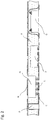
- Figure 2 shows a schematic illustration of an integrated system with the via of the invention.
- the integrated system comprises the via of the invention A; a top interconnect layer B; a bottom interconnect layer C; bare-die with bumps D; solder bumps E; bare-die direct-bond F; bare-die wire bond G; epoxy molding compound H.
- the epoxy molding compound H is the encapsulating second electrically insulating material 5.
- the via of the invention is known as a through-polymer via (TPV).
- TPV through-polymer via
- the TPV is a key technology enabler for 3D integration, packaging and stacking.
- the TPV provides a signal transmission system for 3D integration and contacts suitable for stacking multiple semiconductor components, Microsystems (MEMS) or for mounting components and systems to a next level substrate.
- MEMS Microsystems
- the TPV are suitable for high-volume parallel manufacture.
- the polymer is a photoresist, the position of the TPV can be lithographically defined and is therefore extremely accurate.
- the present invention is therefore providing for low-cost, large scale parallel fabrication of micro-vias for 3D heterogeneous integration and packaging.
- the TPV can be applied to: Integrated circuits, semiconductor die, semiconductor devices, micro-processors, micro-electromechanical systems (MEMS), solid-state lighting, LED, OLED and other (high power) electronics where combinations of high pitch, high input/output density, high aspect ratio, low cost, good electromigration performance and low electrical resistance are required.
- MEMS micro-electromechanical systems
- solid-state lighting LED, OLED and other (high power) electronics where combinations of high pitch, high input/output density, high aspect ratio, low cost, good electromigration performance and low electrical resistance are required.
- the TPV is also applicable to provide interconnects of microfluidic or optical nature.
Landscapes
- Internal Circuitry In Semiconductor Integrated Circuit Devices (AREA)
Description
- The invention relates to vias for three dimensional (3D) stacking, packaging and/or heterogeneous integration of semiconductor devices and/or wafers. In particular, the invention relates to a process for the.manufacture of a via, to a via, to a 3D circuit and to a semiconductor device, including but not limited to a MEMS.
- Vias are interconnects used to vertically interconnect chips, devices, interconnection layers and wafers i.e. in an out-of-plane direction. This may be done either electrical, optical or through micro-fluidic channels.
- State of the art vias include through-silicon vias (TSVs). TSVs are vias that pass through a silicon wafer in order to establish an electrical connection from the active side to the backside of a die. A disadvantage of TSVs is that significant difficulties are often involved with TSV fabrication such as the conformal coverage of complex surfaces, filling of narrow high-aspect-ratio structures, wafer thinning and cracking of the wafer due to material property mismatch with an interposer (e.g. copper) used to form the electrical connection. Furthermore, accurate placement and the electrical connection of the TSV interposer with an interconnect layer is a challenge in itself.
- Another approach is the through mold via (TMV). TMVs are typically formed using a process for epoxy-molding-compound drilling and residue cleaning. Once channels are formed, the vias are completed by filling with solder using for example a screen printing process. This process is not very suitable for 3D integration due to the large diameter of the channel of the via (d≥450µm), low aspect ratio (1:1) and the high resistance of the solder.
-
WO 2006/039633 A2 recites a structure and method of making an interconnect element and multilayer wiring board including the interconnect element. -
US 2006/0267213 A1 recites a stackable tier structure comprising prefabricated high density feedthrough. -
US 2008/0170819 A1 recites an optical element, packaging substrate and device for optical communication. The packaging substrate has a via with a resin filling and a conductor. -
US 2003/0139032 A1 recites a metal post manufacturing method. -
US 2003/0173676 A1 recites a multi-layered semiconductor device and method of manufacturing same. -
US 2010/0218986 A1 recites a method for manufacturing printed wiring board and printed wiring board, -
EP 2 223 581 B1EP 1 681 718 A2KR 2011 0010402 A - It is an object of the invention to overcome disadvantages of vias and of via manufacturing processes of the prior art and/to to provide alternatives thereto.
- In a first aspect, the invention relates to a process for the manufacture of a via for three dimensional stacking, packaging and/or heterogeneous integration of semiconductor devices and/or wafers comprising: (a) providing a microstructure of polymer on a carrier layer or substrate; (b) coating the microstructure with a layer of a first electrically conducting material to provide a coated microstructure; (c) encapsulating the coated microstructure within a second electrically insulating material such that the coated microstructure forms an interconnect between upper and lower surfaces of the second electrically insulating material.
- This approach to manufacturing vias for three dimensional stacking, packaging and/or heterogeneous integration of semiconductor devices and/or wafers is completely different to state of the art processes such as processes for the manufacture of TSVs and TMVs. The process of the invention puts manufacturing the via first, whereas state of the art processes manufactured the via last.
- A notable advantage of the 'via first' approach of the invention is that the process has room for integration of systems, such as semiconductor devices, microfluidic devices and/or MEMS, together with the via in a single step, namely the step of providing the second electrically insulating material. The process is therefore promising for low-cost, large-scale fabrication. This will be clear from the following description. It is remarked that additional interconnection layers can be placed on either side of the via an on top of the second electrically insulating material.
- In the invention, the polymer is a photoresist. Examples of suitable photoresists include SU-8 and dry film photoresist laminate.
- Particular advantages of using photoresist for the microstructures are that even complex structures can be produced with a high degree of accuracy and reproducibility and with dimensions that match or better the dimensions of the state of the art through mold via (TMV) or silicon via. Furthermore the microstructures can be manufactured simultaneously at low cost and in a brief period of time. The exposure and development of the photoresist can take between 30 and 45 minutes.
- Wherein the polymer is a photoresist, providing a microstructure of polymer on a carrier layer or substrate then involves: providing a layer of photoresist on a carrier layer or substrate; patterning (positive or negative depending on whether a positive or negative photoresist is used) the microstructures in the photoresist; exposing the photoresist to a suitable wavelength of radiation (typically UV or even x-ray); exposing the photoresist to a suitable photoresist developer.
- As an alternative, prefabricated (dry film) photoresist microstructures, such as blocks of photoresist can be locally placed, for instance by pick and place equipment, so as to further reduce the cost of producing the via of the invention.
- The layer of photoresist preferably has a thickness in the range of 100 µm to 750 µm. In any case, the height and the width of the microstructure at its widest point is preferably such that the microstructure has an aspect ratio greater than 5, more preferably greater than 10, most preferably greater than 15. High aspect ratios are advantageous from the point of view of miniaturisation of devices etc. incorporating the via.
- In a preferred embodiment, the first electrically conducting material is selected from a group consisting copper, nickel, silver and gold. Coating the microstructures with a layer of copper, nickel, silver or gold is preferably achieved though electro- or electroless-plating, or sputtering and/or evaporation or screen printing. Copper, nickel, silver and gold are excellent conductors and are amenable to electro and electroless plating.
- It is noted that most electrically conducting materials provided as per the process of the invention will provide a functioning via. Alternatives to copper, nickel, silver and gold include certain metals and alloys, conductive polymers, conductive ceramics etc. A person of skill in the art is able to identify suitable examples.
- In an example, encapsulating the microstructure within a second electrically insulating material such that the microstructure forms an interconnect between upper and lower surfaces of the second electrically insulating material comprises encapsulation in epoxy-molding compound. Epoxy molding compounds are epoxy resins such as Bisphenol A Epoxy Resin. It may also be possible to use ceramics or a silicon material, such as in use for stretchable electronics. Examples of suitable electrically insulating materials for the purpose of the invention are known to a person skilled in the art. Such materials are commonly used in e.g. packaging in the field of microelectronics.
- In a preferred embodiment, the process further comprises a step intermediate to steps (a) providing a microstructure of polymer on a carrier layer or substrate, and (b) coating the microstructures with a layer of a first electrically conducting material, of activating the microstructures of polymer towards the first electrically conducting material such as by providing a seed-layer of a third electrically conductive material.
- By activating the polymer towards the first electrically conducting material, the step of coating the microstructures with the material is accelerated.
- A purpose of activating the microstructures of polymer towards the first electrically conducting material is to facilitate and improve adhesion between the layers.
- Activating the microstructures of polymer towards the first electrically conducting material can take many forms and depends on the particular polymer and first electrically conducting materials. Examples of preferred activation methods are given below with reference to the Drawings. Alternative activation methods include for example surface preparation, surface (chemical) modification and coating.
- In a second aspect, the invention relates to a via for three dimensional stacking, packaging and/or heterogeneous integration of semiconductor layers, semiconductor devices, Microsystems and/or wafers comprising a polymer microstructure having a coating of a first electrically conducting material at its surface encapsulated within a second electrically insulating material such that the microstructure forms an interconnect between upper and lower surfaces of the second electrically insulating material. The via of the invention is suitable for application as an electrical interconnect, but may also be applied as optical or microfluidic interconnect, or in general a multi-domain interconnect.
- Advantages of via for 3D integration are: shorter total length of interconnections; lower resistance; reductance in signal delay and avoidance of parasitic capacities and inductances. Particular advantages of the via of the invention relate to miniaturisation, reduced manufacturing complexity and cost; possibility to create 'complex' microstructures.
- In a preferred embodiment the via is a via prepared according to the process of the invention.
- In a preferred embodiment, the polymer is a photoresist.
- Furthermore, the microstructure preferably has an aspect ratio greater than 5, more preferably greater than 10, most preferably greater than 15.
- In a third aspect, the invention relates to a 3D electric circuit having multiple circuit layers wherein the circuit layers are connected by one or more via according to the invention. As mentioned this connection may be electrical, optical or microfluidic.
- In a fourth aspect, the invention relates to a device comprising the 3D electric circuit of the invention.
- The invention will now be further elucidated with reference to the drawings of
Figures 1 and2 . The Figures are provided for illustrative purposes only and are not to be considered as limiting the invention or the appended claims. -
Figure 1 shows a detailed illustration of a preferred embodiment of the process for the manufacture of a via employing micropillars coated with a first electrically conducting material. -
Figure 2 shows a schematic illustration of an integrated system with the via of the invention. - With reference to
Figure 1 : - High-
aspect ratio micro-pillars 2 are created by patterning a thick photoresist on a layer ofsubstrate 1. Two different types of thick photosensitive films have been tested for micro-pillar fabrication. The first type is the well-known SU-8 negative-tone photoresist that is available in a high-viscosity liquid form with a solvent that can be deposited by e.g. spinning or injection molding. The second type are dry film photoresist sheets from SUEX. Advantages of the use of dry film photoresist sheets are that application of the sheets to the substrate results directly in a uniform layer of photoresist having a consistent thickness. Suitable thicknesses of photoresist are typically in the range of 100 µm to 750 µm. The thickness of photoresist layer is determined depending upon the dimensions of the micropillars to be patterned therefrom. It is desirable that the pillars have a high-aspect ratio to facilitate minimising the dimensions of devices etc. fabricated using a via of the invention. - Prior to providing a layer of a first electrically conductive material 4 on the
micropillars 2, themicropillars 2 were first activated by providing a layer, suitably a seed-layer 3, on the micropillars. - Different techniques for layer deposition were tested. The techniques were: (i) Physical vapour deposition (PVD) or sputtering; and (ii) atomic-layer deposition (ALD). The seed layer was provided to activate the micropillars towards electro- and electroless plating (respectively) with copper.
- Physical vapour deposition (PVD) or sputtering of metallic films such as copper or aluminium onto the pillars was used to create a semi-conformal seed layer at low temperature. PVD was performed at ultra-high vacuum to reduce particle contamination and provide good quality films. The main advantage of this method is that it provides a seed layer that can be directly used for plating purposes since it does not require further activation such as through chemical reaction or otherwise by interacting with further compounds. Furthermore, the sputtered films have excellent adhesion to the substrates on which they are sputtered.
- Atomic layer deposition is a self-limiting sequential surface chemistry for the deposition of ultra-thin conformal film. The material used was Titanium nitride (TiN). TiN is electrically conductive, adheres well to metals and has a low processing temperature (<400°C).
- Two different ALD techniques were tested for bringing a thin conformal layer of TiN on the
micropillars 2. High-temperature (400°C) ALD and plasma enhanced ALD, which can be performed at a lower temperature of 150°C. - The result was a conformal layer of TiN i.e. a third seed layer 3 having a thickness of about 60 nm. Prior to plating the TiN with the first electrically conducting material, the TiN was further activated through surface activation with an HF/Pd solution. The HF is used to remove the surface oxide layers on the TiN for the Pd seeding.
- A layer of a first electrically conducting material 4 is provided on top of the seed layer 3.
- Two different methods were then used to provide a layer of a first electrically conducting material 4 on top of the seed layer 3.
- For
micropillars 2 activated by physical vapour deposition or sputtering, the first electrically conducting material 4, in this case, copper was provided directly by electroplating. To prevent corrosion, a further layer of gold was provided on top of the copper layer by electroless plating. - For micropillars activated by ALD and then further activated with HF/Pd solution, electroless plating was used to deposit a layer or nickel. After nickel plating, a layer of gold was again added to prevent corrosion. For thick-film applications, a layer of copper was then deposited on top of the nickel and gold layers (having a thickness of 5-10µm) by electroplating and a further film of gold by electroless plating to prevent corrosion.
- Once the layer of a first electrically conducting material 4 has been provided on the micropillar 2 (and substrate 1) the thus coated micropillar is then encapsulated in a layer of a second electrically insulating material 5. In this example, the electrically insulating material 5 is an epoxy molding compound. The
micropillar 2 is encapsulated such that the coated microstructure forms an interconnect between upper and lower surfaces of the second electrically insulating material 5. - The completed via A is optionally removed from the substrate and back- 6 and top-
side 7 interconnect layers are provided (deposited and patterned). - The
micropillars 2 may have a variety of shapes such as 2a-d. Such shapes cannot easily be created with prior art via manufacturing techniques. - With reference to
Figure 2. Figure 2 shows a schematic illustration of an integrated system with the via of the invention. - The integrated system comprises the via of the invention A; a top interconnect layer B; a bottom interconnect layer C; bare-die with bumps D; solder bumps E; bare-die direct-bond F; bare-die wire bond G; epoxy molding compound H. The epoxy molding compound H is the encapsulating second electrically insulating material 5.
- The via of the invention is known as a through-polymer via (TPV).
- The TPV is a key technology enabler for 3D integration, packaging and stacking. The TPV provides a signal transmission system for 3D integration and contacts suitable for stacking multiple semiconductor components, Microsystems (MEMS) or for mounting components and systems to a next level substrate. Furthermore, the TPV are suitable for high-volume parallel manufacture. Wherein the polymer is a photoresist, the position of the TPV can be lithographically defined and is therefore extremely accurate. The present invention is therefore providing for low-cost, large scale parallel fabrication of micro-vias for 3D heterogeneous integration and packaging.
- The TPV can be applied to: Integrated circuits, semiconductor die, semiconductor devices, micro-processors, micro-electromechanical systems (MEMS), solid-state lighting, LED, OLED and other (high power) electronics where combinations of high pitch, high input/output density, high aspect ratio, low cost, good electromigration performance and low electrical resistance are required. The TPV is also applicable to provide interconnects of microfluidic or optical nature.
Claims (10)
- A process for the manufacture of a via (A) for three dimensional stacking, packaging and/or heterogeneous integration of semiconductor devices and/or wafers comprising:(a) providing a microstructure (2) on a carrier layer or substrate (1);(b) encapsulating the microstructure (2);
characterized by the steps of(c) providing the microstructure as a polymer microstructure (2) embodied as a photoresist;(d) coating the polymer microstructure photoresist (2) with a layer of a first electrically conducting material (4) to provide a coated microstructure;(e) encapsulating the coated microstructure photoresist within a second electrically insulating material (5) such that the coated microstructure photoresist forms an interconnect between upper and lower surfaces of the second electrically insulating material (5). - A process according to claim 1, wherein the microstructure (2) has an aspect ratio greater than 5, more preferably greater than 10, most preferably greater than 15.
- A process according to one or more of the preceding claims, wherein the first electrically conducting material (4) is selected from a group consisting copper, nickel, silver and gold.
- A process according to one or more of the preceding claims, wherein the process further comprises a step intermediate to steps (a) and (b) of claim 1 of activating the microstructures of polymer towards the first electrically conducting material such as by providing a seed-layer of a third electrically conductive material (3).
- A process according to one or more of the preceding claims, wherein the second electrically insulating material is a polymer such as an epoxy-molding compound, or a ceramic material.
- A via (A) for three dimensional stacking, packaging and/or heterogeneous integration of semiconductor devices and/or wafers comprising an interconnect element (I) having a first electrically conducting material (4) at its surface, the interconnect element (I) being encapsulated within a second electrically insulating material (5) such that the interconnect element (I) forms an interconnect between upper and lower surfaces of the second electrically insulating material (5), characterised in that the interconnect element (I) consists of a polymer microstructure (2) photoresist, wherein the first electrically conducting material is provided as a coating at the surface of the microstructure photoresist (2) .
- A via according to claim 6, wherein the microstructure (2) has an aspect ratio greater than 5, more preferably greater than 10, most preferably greater than 15.
- A via according to claim 6 or 7, wherein the first electrically conducting material (4) is selected from a group consisting copper, nickel, silver and gold.
- A 3D electric circuit having multiple circuit layers wherein the circuit layers are electrically, optically or fluidicly connected by at least one via (A) according to any one of claims 6-8.
- A semiconductor device comprising the 3D electric circuit of claim 9.
Applications Claiming Priority (2)
| Application Number | Priority Date | Filing Date | Title |
|---|---|---|---|
| NL2010077A NL2010077C2 (en) | 2013-01-02 | 2013-01-02 | Through-polymer via (tpv) and method to manufacture such a via. |
| PCT/NL2013/050888 WO2014107108A1 (en) | 2013-01-02 | 2013-12-11 | Through-polymer via (tpv) and method to manufacture such a via |
Publications (2)
| Publication Number | Publication Date |
|---|---|
| EP2941785A1 EP2941785A1 (en) | 2015-11-11 |
| EP2941785B1 true EP2941785B1 (en) | 2019-06-19 |
Family
ID=48483139
Family Applications (1)
| Application Number | Title | Priority Date | Filing Date |
|---|---|---|---|
| EP13818479.1A Active EP2941785B1 (en) | 2013-01-02 | 2013-12-11 | Through-polymer via (tpv) and method to manufacture such a via |
Country Status (7)
| Country | Link |
|---|---|
| US (1) | US9576882B2 (en) |
| EP (1) | EP2941785B1 (en) |
| JP (1) | JP6490594B2 (en) |
| KR (1) | KR102235331B1 (en) |
| CN (1) | CN104904009B (en) |
| NL (1) | NL2010077C2 (en) |
| WO (1) | WO2014107108A1 (en) |
Families Citing this family (4)
| Publication number | Priority date | Publication date | Assignee | Title |
|---|---|---|---|---|
| NL2010077C2 (en) | 2013-01-02 | 2014-07-03 | Univ Delft Tech | Through-polymer via (tpv) and method to manufacture such a via. |
| WO2016172089A1 (en) * | 2015-04-21 | 2016-10-27 | Fujifilm Electronic Materials U.S.A., Inc. | Photosensitive polyimide compositions |
| DE102018118765A1 (en) | 2018-08-02 | 2020-02-06 | Endress+Hauser SE+Co. KG | Radio-frequency module |
| KR102745197B1 (en) | 2020-07-28 | 2024-12-23 | 주식회사 엘지에너지솔루션 | The FPCB And The Method For Manufacturing Thereof |
Citations (3)
| Publication number | Priority date | Publication date | Assignee | Title |
|---|---|---|---|---|
| EP1681718A2 (en) * | 2005-01-14 | 2006-07-19 | Seiko Epson Corporation | Electronic component, electro-optical device, and electronic apparatus |
| KR20110010402A (en) * | 2009-07-24 | 2011-02-01 | 한국과학기술원 | Chips having conductive polymer bumps and manufacturing method thereof, Electronic components with chips and manufacturing method thereof |
| EP2223581B1 (en) * | 2007-12-17 | 2014-09-17 | Commissariat à l'Énergie Atomique et aux Énergies Alternatives | Method for making an electric interconnection between two conducting layers |
Family Cites Families (12)
| Publication number | Priority date | Publication date | Assignee | Title |
|---|---|---|---|---|
| US5431328A (en) * | 1994-05-06 | 1995-07-11 | Industrial Technology Research Institute | Composite bump flip chip bonding |
| WO2000077844A1 (en) * | 1999-06-15 | 2000-12-21 | Fujikura Ltd. | Semiconductor package, semiconductor device, electronic device, and method of manufacturing semiconductor package |
| TW502422B (en) * | 2001-06-07 | 2002-09-11 | Ultra Tera Corp | Method for encapsulating thin flip-chip-type semiconductor device |
| TW548816B (en) * | 2002-01-23 | 2003-08-21 | Via Tech Inc | Formation method of conductor pillar |
| JP2003264253A (en) * | 2002-03-12 | 2003-09-19 | Shinko Electric Ind Co Ltd | Semiconductor device and manufacturing method thereof |
| US7250712B2 (en) * | 2004-01-21 | 2007-07-31 | Lumera Corporation | Polymer sustained microelectrodes |
| JP2006108211A (en) * | 2004-10-01 | 2006-04-20 | North:Kk | Wiring board, multilayer wiring board using the wiring board, and method for manufacturing the multilayer wiring board |
| US7919844B2 (en) * | 2005-05-26 | 2011-04-05 | Aprolase Development Co., Llc | Tier structure with tier frame having a feedthrough structure |
| US7768113B2 (en) * | 2005-05-26 | 2010-08-03 | Volkan Ozguz | Stackable tier structure comprising prefabricated high density feedthrough |
| US7907801B2 (en) * | 2007-01-17 | 2011-03-15 | Ibiden Co., Ltd. | Optical element, package substrate and device for optical communication |
| US8153905B2 (en) * | 2009-02-27 | 2012-04-10 | Ibiden Co., Ltd. | Method for manufacturing printed wiring board and printed wiring board |
| NL2010077C2 (en) | 2013-01-02 | 2014-07-03 | Univ Delft Tech | Through-polymer via (tpv) and method to manufacture such a via. |
-
2013
- 2013-01-02 NL NL2010077A patent/NL2010077C2/en not_active IP Right Cessation
- 2013-12-11 CN CN201380069223.7A patent/CN104904009B/en active Active
- 2013-12-11 WO PCT/NL2013/050888 patent/WO2014107108A1/en not_active Ceased
- 2013-12-11 JP JP2015551657A patent/JP6490594B2/en active Active
- 2013-12-11 KR KR1020157020925A patent/KR102235331B1/en active Active
- 2013-12-11 EP EP13818479.1A patent/EP2941785B1/en active Active
-
2015
- 2015-06-30 US US14/788,275 patent/US9576882B2/en active Active
Patent Citations (3)
| Publication number | Priority date | Publication date | Assignee | Title |
|---|---|---|---|---|
| EP1681718A2 (en) * | 2005-01-14 | 2006-07-19 | Seiko Epson Corporation | Electronic component, electro-optical device, and electronic apparatus |
| EP2223581B1 (en) * | 2007-12-17 | 2014-09-17 | Commissariat à l'Énergie Atomique et aux Énergies Alternatives | Method for making an electric interconnection between two conducting layers |
| KR20110010402A (en) * | 2009-07-24 | 2011-02-01 | 한국과학기술원 | Chips having conductive polymer bumps and manufacturing method thereof, Electronic components with chips and manufacturing method thereof |
Also Published As
| Publication number | Publication date |
|---|---|
| US20150303131A1 (en) | 2015-10-22 |
| JP6490594B2 (en) | 2019-03-27 |
| US9576882B2 (en) | 2017-02-21 |
| WO2014107108A1 (en) | 2014-07-10 |
| JP2016505217A (en) | 2016-02-18 |
| EP2941785A1 (en) | 2015-11-11 |
| KR20150103719A (en) | 2015-09-11 |
| CN104904009B (en) | 2019-04-09 |
| CN104904009A (en) | 2015-09-09 |
| NL2010077C2 (en) | 2014-07-03 |
| HK1216121A1 (en) | 2016-10-14 |
| KR102235331B1 (en) | 2021-04-02 |
Similar Documents
| Publication | Publication Date | Title |
|---|---|---|
| US7538032B2 (en) | Low temperature method for fabricating high-aspect ratio vias and devices fabricated by said method | |
| US7932608B2 (en) | Through-silicon via formed with a post passivation interconnect structure | |
| US6908856B2 (en) | Method for producing electrical through hole interconnects and devices made thereof | |
| KR100831405B1 (en) | Wafer Bonding Packaging Method | |
| US8741691B2 (en) | Method of fabricating three dimensional integrated circuit | |
| EP1519410A1 (en) | Method for producing electrical through hole interconnects and devices made thereof | |
| SE537874C2 (en) | CTE-adapted interposer and method of manufacturing one | |
| EP3316283B1 (en) | Method of fabricating a through substrate via | |
| CN110970397A (en) | Stack packaging structure and preparation method thereof | |
| US9576882B2 (en) | Through polymer via (TPV) and method to manufacture such a via | |
| CN101645401A (en) | Circuit device three-dimensional integrative method | |
| CN101814477B (en) | A Silicon through holes after the interlinked structure being passivated. | |
| US20040195669A1 (en) | Integrated circuit packaging apparatus and method | |
| JP5204789B2 (en) | Formation of plated pillar package | |
| US20140263582A1 (en) | Low cost interposer and method of fabrication | |
| US20130130439A1 (en) | Formed metallic heat sink substrate, circuit system, and fabrication methods | |
| EP2704187B1 (en) | METHOD FOR PRODUCING ELECTRICAL THROUGH HOLE INTERCONNECTS AND corresponding DEVICE | |
| HK1216121B (en) | Through-polymer via (tpv) and method to manufacture such a via | |
| CN113544827B (en) | Packaging method and packaging structure of chip | |
| CN116996036A (en) | Silicon-based MEMS radio frequency filter and preparation method thereof | |
| Hamelink et al. | Through-polymer-via for 3D heterogeneous integration and packaging | |
| CN111477552A (en) | CMOS-MEMS double-sided integrated chip and integration method thereof | |
| WO2006086337A1 (en) | A low temperature method for fabricating high-aspect ratio vias and devices fabricated by said method | |
| CN119694891A (en) | A heterogeneous 3D adapter plate structure and preparation method thereof | |
| CN114429935A (en) | Manufacturing method of metal interconnection structure |
Legal Events
| Date | Code | Title | Description |
|---|---|---|---|
| PUAI | Public reference made under article 153(3) epc to a published international application that has entered the european phase |
Free format text: ORIGINAL CODE: 0009012 |
|
| 17P | Request for examination filed |
Effective date: 20150629 |
|
| AK | Designated contracting states |
Kind code of ref document: A1 Designated state(s): AL AT BE BG CH CY CZ DE DK EE ES FI FR GB GR HR HU IE IS IT LI LT LU LV MC MK MT NL NO PL PT RO RS SE SI SK SM TR |
|
| AX | Request for extension of the european patent |
Extension state: BA ME |
|
| DAX | Request for extension of the european patent (deleted) | ||
| REG | Reference to a national code |
Ref country code: HK Ref legal event code: DE Ref document number: 1216121 Country of ref document: HK |
|
| 17Q | First examination report despatched |
Effective date: 20160928 |
|
| STAA | Information on the status of an ep patent application or granted ep patent |
Free format text: STATUS: EXAMINATION IS IN PROGRESS |
|
| RIC1 | Information provided on ipc code assigned before grant |
Ipc: H01L 21/56 20060101ALI20181129BHEP Ipc: H01L 23/538 20060101ALI20181129BHEP Ipc: H01L 25/10 20060101ALI20181129BHEP Ipc: H01L 23/00 20060101ALI20181129BHEP Ipc: H01L 21/48 20060101ALI20181129BHEP Ipc: H01L 23/498 20060101AFI20181129BHEP |
|
| GRAP | Despatch of communication of intention to grant a patent |
Free format text: ORIGINAL CODE: EPIDOSNIGR1 |
|
| STAA | Information on the status of an ep patent application or granted ep patent |
Free format text: STATUS: GRANT OF PATENT IS INTENDED |
|
| RAP1 | Party data changed (applicant data changed or rights of an application transferred) |
Owner name: ADVANCED PACKAGING CENTER B.V. |
|
| INTG | Intention to grant announced |
Effective date: 20190121 |
|
| GRAS | Grant fee paid |
Free format text: ORIGINAL CODE: EPIDOSNIGR3 |
|
| GRAA | (expected) grant |
Free format text: ORIGINAL CODE: 0009210 |
|
| STAA | Information on the status of an ep patent application or granted ep patent |
Free format text: STATUS: THE PATENT HAS BEEN GRANTED |
|
| AK | Designated contracting states |
Kind code of ref document: B1 Designated state(s): AL AT BE BG CH CY CZ DE DK EE ES FI FR GB GR HR HU IE IS IT LI LT LU LV MC MK MT NL NO PL PT RO RS SE SI SK SM TR |
|
| REG | Reference to a national code |
Ref country code: GB Ref legal event code: FG4D |
|
| REG | Reference to a national code |
Ref country code: CH Ref legal event code: EP |
|
| REG | Reference to a national code |
Ref country code: IE Ref legal event code: FG4D |
|
| REG | Reference to a national code |
Ref country code: DE Ref legal event code: R096 Ref document number: 602013056879 Country of ref document: DE |
|
| REG | Reference to a national code |
Ref country code: AT Ref legal event code: REF Ref document number: 1146580 Country of ref document: AT Kind code of ref document: T Effective date: 20190715 |
|
| REG | Reference to a national code |
Ref country code: NL Ref legal event code: FP |
|
| PG25 | Lapsed in a contracting state [announced via postgrant information from national office to epo] |
Ref country code: HR Free format text: LAPSE BECAUSE OF FAILURE TO SUBMIT A TRANSLATION OF THE DESCRIPTION OR TO PAY THE FEE WITHIN THE PRESCRIBED TIME-LIMIT Effective date: 20190619 Ref country code: LT Free format text: LAPSE BECAUSE OF FAILURE TO SUBMIT A TRANSLATION OF THE DESCRIPTION OR TO PAY THE FEE WITHIN THE PRESCRIBED TIME-LIMIT Effective date: 20190619 Ref country code: FI Free format text: LAPSE BECAUSE OF FAILURE TO SUBMIT A TRANSLATION OF THE DESCRIPTION OR TO PAY THE FEE WITHIN THE PRESCRIBED TIME-LIMIT Effective date: 20190619 Ref country code: SE Free format text: LAPSE BECAUSE OF FAILURE TO SUBMIT A TRANSLATION OF THE DESCRIPTION OR TO PAY THE FEE WITHIN THE PRESCRIBED TIME-LIMIT Effective date: 20190619 Ref country code: AL Free format text: LAPSE BECAUSE OF FAILURE TO SUBMIT A TRANSLATION OF THE DESCRIPTION OR TO PAY THE FEE WITHIN THE PRESCRIBED TIME-LIMIT Effective date: 20190619 Ref country code: NO Free format text: LAPSE BECAUSE OF FAILURE TO SUBMIT A TRANSLATION OF THE DESCRIPTION OR TO PAY THE FEE WITHIN THE PRESCRIBED TIME-LIMIT Effective date: 20190919 |
|
| REG | Reference to a national code |
Ref country code: LT Ref legal event code: MG4D |
|
| PG25 | Lapsed in a contracting state [announced via postgrant information from national office to epo] |
Ref country code: BG Free format text: LAPSE BECAUSE OF FAILURE TO SUBMIT A TRANSLATION OF THE DESCRIPTION OR TO PAY THE FEE WITHIN THE PRESCRIBED TIME-LIMIT Effective date: 20190919 Ref country code: RS Free format text: LAPSE BECAUSE OF FAILURE TO SUBMIT A TRANSLATION OF THE DESCRIPTION OR TO PAY THE FEE WITHIN THE PRESCRIBED TIME-LIMIT Effective date: 20190619 Ref country code: GR Free format text: LAPSE BECAUSE OF FAILURE TO SUBMIT A TRANSLATION OF THE DESCRIPTION OR TO PAY THE FEE WITHIN THE PRESCRIBED TIME-LIMIT Effective date: 20190920 Ref country code: LV Free format text: LAPSE BECAUSE OF FAILURE TO SUBMIT A TRANSLATION OF THE DESCRIPTION OR TO PAY THE FEE WITHIN THE PRESCRIBED TIME-LIMIT Effective date: 20190619 |
|
| REG | Reference to a national code |
Ref country code: AT Ref legal event code: MK05 Ref document number: 1146580 Country of ref document: AT Kind code of ref document: T Effective date: 20190619 |
|
| PG25 | Lapsed in a contracting state [announced via postgrant information from national office to epo] |
Ref country code: PT Free format text: LAPSE BECAUSE OF FAILURE TO SUBMIT A TRANSLATION OF THE DESCRIPTION OR TO PAY THE FEE WITHIN THE PRESCRIBED TIME-LIMIT Effective date: 20191021 Ref country code: EE Free format text: LAPSE BECAUSE OF FAILURE TO SUBMIT A TRANSLATION OF THE DESCRIPTION OR TO PAY THE FEE WITHIN THE PRESCRIBED TIME-LIMIT Effective date: 20190619 Ref country code: AT Free format text: LAPSE BECAUSE OF FAILURE TO SUBMIT A TRANSLATION OF THE DESCRIPTION OR TO PAY THE FEE WITHIN THE PRESCRIBED TIME-LIMIT Effective date: 20190619 Ref country code: SK Free format text: LAPSE BECAUSE OF FAILURE TO SUBMIT A TRANSLATION OF THE DESCRIPTION OR TO PAY THE FEE WITHIN THE PRESCRIBED TIME-LIMIT Effective date: 20190619 Ref country code: RO Free format text: LAPSE BECAUSE OF FAILURE TO SUBMIT A TRANSLATION OF THE DESCRIPTION OR TO PAY THE FEE WITHIN THE PRESCRIBED TIME-LIMIT Effective date: 20190619 Ref country code: CZ Free format text: LAPSE BECAUSE OF FAILURE TO SUBMIT A TRANSLATION OF THE DESCRIPTION OR TO PAY THE FEE WITHIN THE PRESCRIBED TIME-LIMIT Effective date: 20190619 |
|
| PG25 | Lapsed in a contracting state [announced via postgrant information from national office to epo] |
Ref country code: IS Free format text: LAPSE BECAUSE OF FAILURE TO SUBMIT A TRANSLATION OF THE DESCRIPTION OR TO PAY THE FEE WITHIN THE PRESCRIBED TIME-LIMIT Effective date: 20191019 Ref country code: SM Free format text: LAPSE BECAUSE OF FAILURE TO SUBMIT A TRANSLATION OF THE DESCRIPTION OR TO PAY THE FEE WITHIN THE PRESCRIBED TIME-LIMIT Effective date: 20190619 Ref country code: ES Free format text: LAPSE BECAUSE OF FAILURE TO SUBMIT A TRANSLATION OF THE DESCRIPTION OR TO PAY THE FEE WITHIN THE PRESCRIBED TIME-LIMIT Effective date: 20190619 |
|
| PG25 | Lapsed in a contracting state [announced via postgrant information from national office to epo] |
Ref country code: TR Free format text: LAPSE BECAUSE OF FAILURE TO SUBMIT A TRANSLATION OF THE DESCRIPTION OR TO PAY THE FEE WITHIN THE PRESCRIBED TIME-LIMIT Effective date: 20190619 |
|
| PG25 | Lapsed in a contracting state [announced via postgrant information from national office to epo] |
Ref country code: DK Free format text: LAPSE BECAUSE OF FAILURE TO SUBMIT A TRANSLATION OF THE DESCRIPTION OR TO PAY THE FEE WITHIN THE PRESCRIBED TIME-LIMIT Effective date: 20190619 Ref country code: PL Free format text: LAPSE BECAUSE OF FAILURE TO SUBMIT A TRANSLATION OF THE DESCRIPTION OR TO PAY THE FEE WITHIN THE PRESCRIBED TIME-LIMIT Effective date: 20190619 |
|
| PG25 | Lapsed in a contracting state [announced via postgrant information from national office to epo] |
Ref country code: IS Free format text: LAPSE BECAUSE OF FAILURE TO SUBMIT A TRANSLATION OF THE DESCRIPTION OR TO PAY THE FEE WITHIN THE PRESCRIBED TIME-LIMIT Effective date: 20200224 |
|
| REG | Reference to a national code |
Ref country code: DE Ref legal event code: R097 Ref document number: 602013056879 Country of ref document: DE |
|
| PLBE | No opposition filed within time limit |
Free format text: ORIGINAL CODE: 0009261 |
|
| STAA | Information on the status of an ep patent application or granted ep patent |
Free format text: STATUS: NO OPPOSITION FILED WITHIN TIME LIMIT |
|
| PG2D | Information on lapse in contracting state deleted |
Ref country code: IS |
|
| REG | Reference to a national code |
Ref country code: CH Ref legal event code: PL |
|
| 26N | No opposition filed |
Effective date: 20200603 |
|
| PG25 | Lapsed in a contracting state [announced via postgrant information from national office to epo] |
Ref country code: MC Free format text: LAPSE BECAUSE OF FAILURE TO SUBMIT A TRANSLATION OF THE DESCRIPTION OR TO PAY THE FEE WITHIN THE PRESCRIBED TIME-LIMIT Effective date: 20190619 Ref country code: SI Free format text: LAPSE BECAUSE OF FAILURE TO SUBMIT A TRANSLATION OF THE DESCRIPTION OR TO PAY THE FEE WITHIN THE PRESCRIBED TIME-LIMIT Effective date: 20190619 |
|
| PG25 | Lapsed in a contracting state [announced via postgrant information from national office to epo] |
Ref country code: LU Free format text: LAPSE BECAUSE OF NON-PAYMENT OF DUE FEES Effective date: 20191211 Ref country code: IE Free format text: LAPSE BECAUSE OF NON-PAYMENT OF DUE FEES Effective date: 20191211 |
|
| PG25 | Lapsed in a contracting state [announced via postgrant information from national office to epo] |
Ref country code: LI Free format text: LAPSE BECAUSE OF NON-PAYMENT OF DUE FEES Effective date: 20191231 Ref country code: CH Free format text: LAPSE BECAUSE OF NON-PAYMENT OF DUE FEES Effective date: 20191231 |
|
| PG25 | Lapsed in a contracting state [announced via postgrant information from national office to epo] |
Ref country code: CY Free format text: LAPSE BECAUSE OF FAILURE TO SUBMIT A TRANSLATION OF THE DESCRIPTION OR TO PAY THE FEE WITHIN THE PRESCRIBED TIME-LIMIT Effective date: 20190619 |
|
| PG25 | Lapsed in a contracting state [announced via postgrant information from national office to epo] |
Ref country code: MT Free format text: LAPSE BECAUSE OF FAILURE TO SUBMIT A TRANSLATION OF THE DESCRIPTION OR TO PAY THE FEE WITHIN THE PRESCRIBED TIME-LIMIT Effective date: 20190619 Ref country code: HU Free format text: LAPSE BECAUSE OF FAILURE TO SUBMIT A TRANSLATION OF THE DESCRIPTION OR TO PAY THE FEE WITHIN THE PRESCRIBED TIME-LIMIT; INVALID AB INITIO Effective date: 20131211 |
|
| PG25 | Lapsed in a contracting state [announced via postgrant information from national office to epo] |
Ref country code: MK Free format text: LAPSE BECAUSE OF FAILURE TO SUBMIT A TRANSLATION OF THE DESCRIPTION OR TO PAY THE FEE WITHIN THE PRESCRIBED TIME-LIMIT Effective date: 20190619 |
|
| REG | Reference to a national code |
Ref country code: DE Ref legal event code: R079 Ref document number: 602013056879 Country of ref document: DE Free format text: PREVIOUS MAIN CLASS: H01L0023498000 Ipc: H10W0070620000 |
|
| PGFP | Annual fee paid to national office [announced via postgrant information from national office to epo] |
Ref country code: GB Payment date: 20251229 Year of fee payment: 13 |
|
| PGFP | Annual fee paid to national office [announced via postgrant information from national office to epo] |
Ref country code: IT Payment date: 20251219 Year of fee payment: 13 |
|
| PGFP | Annual fee paid to national office [announced via postgrant information from national office to epo] |
Ref country code: NL Payment date: 20251226 Year of fee payment: 13 Ref country code: FR Payment date: 20251226 Year of fee payment: 13 |
|
| PGFP | Annual fee paid to national office [announced via postgrant information from national office to epo] |
Ref country code: BE Payment date: 20251229 Year of fee payment: 13 |
|
| PGFP | Annual fee paid to national office [announced via postgrant information from national office to epo] |
Ref country code: DE Payment date: 20251229 Year of fee payment: 13 |